KR100269306B1 - Integrate circuit device having buffer layer containing metal oxide stabilized by low temperature treatment and fabricating method thereof - Google Patents
Integrate circuit device having buffer layer containing metal oxide stabilized by low temperature treatment and fabricating method thereofDownload PDFInfo
- Publication number
- KR100269306B1 KR100269306B1KR1019970036558AKR19970036558AKR100269306B1KR 100269306 B1KR100269306 B1KR 100269306B1KR 1019970036558 AKR1019970036558 AKR 1019970036558AKR 19970036558 AKR19970036558 AKR 19970036558AKR 100269306 B1KR100269306 B1KR 100269306B1
- Authority
- KR
- South Korea
- Prior art keywords
- film
- pattern
- aluminum oxide
- oxide film
- film pattern
- Prior art date
- Legal status (The legal status is an assumption and is not a legal conclusion. Google has not performed a legal analysis and makes no representation as to the accuracy of the status listed.)
- Expired - Fee Related
Links
Images


Classifications
- H—ELECTRICITY
- H10—SEMICONDUCTOR DEVICES; ELECTRIC SOLID-STATE DEVICES NOT OTHERWISE PROVIDED FOR
- H10D—INORGANIC ELECTRIC SEMICONDUCTOR DEVICES
- H10D84/00—Integrated devices formed in or on semiconductor substrates that comprise only semiconducting layers, e.g. on Si wafers or on GaAs-on-Si wafers
- H—ELECTRICITY
- H10—SEMICONDUCTOR DEVICES; ELECTRIC SOLID-STATE DEVICES NOT OTHERWISE PROVIDED FOR
- H10D—INORGANIC ELECTRIC SEMICONDUCTOR DEVICES
- H10D1/00—Resistors, capacitors or inductors
- H10D1/60—Capacitors
- H10D1/68—Capacitors having no potential barriers
- H10D1/692—Electrodes
- H10D1/696—Electrodes comprising multiple layers, e.g. comprising a barrier layer and a metal layer
- H—ELECTRICITY
- H10—SEMICONDUCTOR DEVICES; ELECTRIC SOLID-STATE DEVICES NOT OTHERWISE PROVIDED FOR
- H10D—INORGANIC ELECTRIC SEMICONDUCTOR DEVICES
- H10D84/00—Integrated devices formed in or on semiconductor substrates that comprise only semiconducting layers, e.g. on Si wafers or on GaAs-on-Si wafers
- H10D84/80—Integrated devices formed in or on semiconductor substrates that comprise only semiconducting layers, e.g. on Si wafers or on GaAs-on-Si wafers characterised by the integration of at least one component covered by groups H10D12/00 or H10D30/00, e.g. integration of IGFETs
- H—ELECTRICITY
- H01—ELECTRIC ELEMENTS
- H01L—SEMICONDUCTOR DEVICES NOT COVERED BY CLASS H10
- H01L21/00—Processes or apparatus adapted for the manufacture or treatment of semiconductor or solid state devices or of parts thereof
- H01L21/02—Manufacture or treatment of semiconductor devices or of parts thereof
- H01L21/04—Manufacture or treatment of semiconductor devices or of parts thereof the devices having potential barriers, e.g. a PN junction, depletion layer or carrier concentration layer
- H01L21/18—Manufacture or treatment of semiconductor devices or of parts thereof the devices having potential barriers, e.g. a PN junction, depletion layer or carrier concentration layer the devices having semiconductor bodies comprising elements of Group IV of the Periodic Table or AIIIBV compounds with or without impurities, e.g. doping materials
- H01L21/28—Manufacture of electrodes on semiconductor bodies using processes or apparatus not provided for in groups H01L21/20 - H01L21/268
- H01L21/283—Deposition of conductive or insulating materials for electrodes conducting electric current
- H01L21/285—Deposition of conductive or insulating materials for electrodes conducting electric current from a gas or vapour, e.g. condensation
- H01L21/28506—Deposition of conductive or insulating materials for electrodes conducting electric current from a gas or vapour, e.g. condensation of conductive layers
- H01L21/28512—Deposition of conductive or insulating materials for electrodes conducting electric current from a gas or vapour, e.g. condensation of conductive layers on semiconductor bodies comprising elements of Group IV of the Periodic Table
- H01L21/28568—Deposition of conductive or insulating materials for electrodes conducting electric current from a gas or vapour, e.g. condensation of conductive layers on semiconductor bodies comprising elements of Group IV of the Periodic Table the conductive layers comprising transition metals
- H—ELECTRICITY
- H10—SEMICONDUCTOR DEVICES; ELECTRIC SOLID-STATE DEVICES NOT OTHERWISE PROVIDED FOR
- H10B—ELECTRONIC MEMORY DEVICES
- H10B12/00—Dynamic random access memory [DRAM] devices
- H10B12/01—Manufacture or treatment
- H10B12/02—Manufacture or treatment for one transistor one-capacitor [1T-1C] memory cells
- H10B12/03—Making the capacitor or connections thereto
- H10B12/033—Making the capacitor or connections thereto the capacitor extending over the transistor
- H—ELECTRICITY
- H10—SEMICONDUCTOR DEVICES; ELECTRIC SOLID-STATE DEVICES NOT OTHERWISE PROVIDED FOR
- H10D—INORGANIC ELECTRIC SEMICONDUCTOR DEVICES
- H10D1/00—Resistors, capacitors or inductors
- H10D1/60—Capacitors
- H10D1/68—Capacitors having no potential barriers
- H10D1/682—Capacitors having no potential barriers having dielectrics comprising perovskite structures
Landscapes
- Semiconductor Memories (AREA)
- Semiconductor Integrated Circuits (AREA)
- Non-Volatile Memory (AREA)
Abstract
Translated fromKoreanDescription
Translated fromKorean본 발명은 마이크로 전자 공학 분야에 관련된 것으로, 특히 저온 처리로 안정화되는 금속 산화막으로 구성된 완충막을 구비하는 집적 회로 장치 및 그 제조방법에 관한 것이다.BACKGROUND OF THE
DRAM 소자에서 정보는 메모리 셀 커패시터에 전하의 형태로 저장된다. 이 저장된 전하는 시간이 지나면서 여러 경로를 통해 소실된다. 따라서 주기적으로 정보를 재생시키는 리프레쉬(refresh)동작이 필요하다. 이러한 리프레쉬 동작간의 간격을 리프레쉬 타임이라고 한다. 이러한 리프레쉬 타임은 커패시터의 용량을 증가시켜 메모리 셀 커패시터에 의해 저장되는 전하량(Q)을 증가시킴으로써 개선할 수 있다.In DRAM devices, information is stored in the form of charge in memory cell capacitors. This stored charge is lost through several paths over time. Therefore, there is a need for a refresh operation to periodically refresh information. The interval between such refresh operations is called refresh time. This refresh time can be improved by increasing the capacitance of the capacitor to increase the amount of charge Q stored by the memory cell capacitor.
커패시터의 용량을 증가시키기 위한 방법으로 널리 사용되는 방법중의 하나가 고유전율의 강유전체 물질 또는 고유전율의 상유전체 물질(이하 이들 물질을 고유전체 물질이라 함)을 커패시터의 유전막으로 사용하는 방법이 있다. 고유전체막을 유전막으로 포함하는 커패시터의 전 표면에는 후속 공정에서 형성되는 금속 배선 등과의 절연을 목적으로 하는 층간 절연막, 예컨대 실리콘 산화막등이 형성되게 된다. 그러나 실리콘 산화막을 고유전체막과 직접 접촉시키게 되면 양자간의 반응에 의해 커패시터의 특성이 열화되고 전극물질과 접촉하는 실리콘 산화막내에 크랙이 발생한다. 이러한 문제점을 방지하고 후속 공정시 고유전체막을 이루고 있는 물질들이 휘발되어 확산되거나 수소가 고유전체막으로 침투하는 것을 방지하기 위하여, 고유전체막과 백금 전극으로 이루어진 커패시터와 층간 절연막인 실리콘 산화막 사이에 TiO2막등을 완충막으로 형성한 구조 및 그 제조방법이 미국 특허 번호 제 5,212,620에 개시되어 있다.One of the widely used methods to increase the capacitance of a capacitor is to use a high dielectric constant ferroelectric material or a high dielectric constant dielectric material (hereinafter, these materials are referred to as high dielectric materials) as the dielectric film of the capacitor. . On the entire surface of the capacitor including the high dielectric film as a dielectric film, an interlayer insulating film, for example, a silicon oxide film or the like, is formed to insulate the metal wiring and the like formed in a subsequent step. However, when the silicon oxide film is in direct contact with the high-k dielectric film, the characteristics of the capacitor deteriorate due to the reaction between them and cracks occur in the silicon oxide film in contact with the electrode material. In order to prevent such a problem and to prevent volatilization and diffusion of materials constituting the high dielectric film in a subsequent process, or hydrogen to penetrate into the high dielectric film, a TiO is interposed between a capacitor composed of a high dielectric film and a platinum electrode and a silicon oxide film as an interlayer insulating film. A structure in whichtwo films and the like are formed as a buffer film and a manufacturing method thereof are disclosed in US Patent No. 5,212,620.
상기 미국 특허에 따르면 티타늄(Ti)막을 형성한 후, 산소분위기하에서 650℃로 열처리함으로써 티타늄 산화막(TiO2)을 형성한다. 티타늄 산화막은 650℃ 이상으로 열처리해야만 완충막으로서 충분한 기능을 수행할 수 있게된다. 만약 650℃ 이하로 열처리를 하게 되면 티타늄막이 티타늄 산화막으로 완전히 산화되는 것이 아니라 TiO 또는 TiOx등으로 불완전하게 산화되기 때문이다. 불완전 산화된 완충막은 비저항값이 낮기 때문에 커패시터의 상, 하부 전극간에 누설 전류가 증가하게 된다. 또한 티타늄 산화막은 스퍼터링에 의해 형성하므로 단차 피복력이 낮고 일정 두께 이상으로 형성하여야만 하는 제한 조건이 따른다.According to the US patent, a titanium (Ti) film is formed, and then a titanium oxide film (TiO2 ) is formed by heat treatment at 650 ° C. under an oxygen atmosphere. The titanium oxide film must be heat-treated at 650 ° C. or higher to perform a sufficient function as a buffer film. If the heat treatment below 650 ℃ titanium film is not completely oxidized to titanium oxide film, but is incompletely oxidized to TiO or TiOx . Since the incompletely oxidized buffer film has a low specific resistance, leakage current increases between upper and lower electrodes of the capacitor. In addition, since the titanium oxide film is formed by sputtering, there is a restriction condition that the step coverage is low and must be formed over a predetermined thickness.
그런데 콘택 플러그와 커패시터 하부 전극간의 충분한 콘택 저항을 확보하기 위해서는 커패시터 형성 이후의 공정을 600℃ 이하의 저온에서 실시할 것이 요구된다. 일례로서, 600℃ 이상의 고온 처리를 하게되면 하부 전극을 구성하는 물질이 콘택 플러그로 확산되는 것을 방지하기 위하여 형성한 장벽 금속막의 막질이 변화하여서 확산방지막으로서의 기능을 제대로 수행하지 못하게 된다.However, in order to secure sufficient contact resistance between the contact plug and the lower electrode of the capacitor, it is required to perform the process after capacitor formation at a low temperature of 600 ° C or lower. For example, when the high temperature treatment is performed at 600 ° C. or higher, the film quality of the barrier metal film formed to prevent the material constituting the lower electrode from being diffused into the contact plug is changed to prevent the function of the diffusion barrier.
따라서, 650℃이상의 고온 열처리를 요구하는 티타늄 산화막은 저온 열처리가 절실히 요구되는 고집적화된 집적 회로 장치에 부적합하다.Therefore, the titanium oxide film requiring high temperature heat treatment of 650 DEG C or higher is unsuitable for highly integrated integrated circuit devices in which low temperature heat treatment is urgently required.
따라서 본 발명이 이루고자 하는 기술적 과제는 상술한 종래 기술이 갖는 문제점을 해결하기 위하여 저온 처리로 안정화되는 금속 산화막으로 이루어진 완충막을 구비하는 집적 회로 장치를 제공하는 것이다.Accordingly, an object of the present invention is to provide an integrated circuit device having a buffer film made of a metal oxide film stabilized by low temperature treatment in order to solve the problems of the prior art.
본 발명의 다른 기술적 과제는 상기 집적 회로 장치를 제조하는데 적합한 제조방법을 제공하는 것이다.Another technical problem of the present invention is to provide a manufacturing method suitable for manufacturing the integrated circuit device.
도 1은 본 발명의 제1 실시예에 따른 집적 회로 장치의 단면도를 나타낸다.1 shows a cross-sectional view of an integrated circuit device according to a first embodiment of the present invention.
도 2 는 본 발명의 제2 실시예에 따른 집적 회로 장치의 단면도를 나타낸다.2 shows a cross-sectional view of an integrated circuit device according to a second embodiment of the present invention.
도 3 은 본 발명의 제3 실시예에 따른 집적 회로 장치의 단면도를 나타낸다.3 shows a cross-sectional view of an integrated circuit device according to a third embodiment of the present invention.
도 4는 본 발명의 제4 실시예에 따른 스위칭 소자의 단면도를 나타낸다.4 is a sectional view of a switching device according to a fourth embodiment of the present invention.
도 5 내지 도 7 은 본 발명의 제1 실시예에 따른 집적 회로 장치의 제조방법을 설명하기 위한 제조 공정 중간 단계 구조물들의 단면도를 나타낸다.5 to 7 illustrate cross-sectional views of structures in an intermediate stage of a manufacturing process for explaining a method of manufacturing an integrated circuit device according to a first exemplary embodiment of the present invention.
도 8 내지 도 11은 본 발명의 제2 실시예에 따른 집적 회로 장치의 제조 방법을 설명하기 위한 제조 공정 중간 단계 구조물들의 단면도를 나타낸다.8 to 11 illustrate cross-sectional views of intermediate steps of a manufacturing process for explaining a method of manufacturing an integrated circuit device according to a second exemplary embodiment of the present invention.
도 12 내지 도 14는 본 발명의 제4 실시예에 따른 스위칭 소자의 제조 방법을 설명하기 위한 제조 공정 중간 단계 구조물들의 단면도를 나타낸다.12 to 14 illustrate cross-sectional views of structures in an intermediate stage of a manufacturing process for explaining a method of manufacturing a switching device according to a fourth exemplary embodiment of the present invention.
도 15a 내지 도 15c는 알루미늄 산화막 증착 후에 측정한 분극 특성을 나타내는 그래프들이다.15A to 15C are graphs showing polarization characteristics measured after aluminum oxide film deposition.
도 16a 내지 도 16b 어닐링 후에 측정한 분극 특성을 나타내는 그래프들이다.16A to 16B are graphs showing polarization characteristics measured after annealing.
도 17은 알루미늄 산화막 형성 조건에 따른 잔류 분극 값을 나타내는 그래프이다.17 is a graph showing residual polarization values according to aluminum oxide film formation conditions.
도 18은 알루미늄 산화막 형성 조건에 따른 누설 전류 값을 나타내는 그래프이다.18 is a graph showing leakage current values according to aluminum oxide film formation conditions.
도 19는 실리콘 산화막 증착 후 측정한 잔류 분극 값을 나타내는 그래프이다.19 is a graph showing residual polarization values measured after deposition of a silicon oxide film.
도 20은 실리콘 산화막 증착 후 측정한 누설 전류 값을 나타내는 그래프이다.20 is a graph showing leakage current values measured after deposition of a silicon oxide film.
도 21은 NH3플라즈마 처리 전과 후에 측정한 분극 특성을 나타내는 그래프이다.21 is a graph showing polarization characteristics measured before and after NH3 plasma treatment.
도 22는 알루미늄 산화막 어닐링 후에 측정한 BST 커패시터의 커패시턴스를 나타내는 그래프이다.22 is a graph showing the capacitance of the BST capacitor measured after aluminum oxide film annealing.
도 23은 알루미늄 산화막 어닐링 후에 측정한 BST 커패시터의 누설 전류를 나타내는 그래프이다.Fig. 23 is a graph showing the leakage current of the BST capacitor measured after aluminum oxide film annealing.
본 발명에 따르면, 상기 기술적 과제는, 600℃ 이하의 저온 처리로 안정화되는 금속 산화막으로 이루어지고, 고유전체막을 포함하는 막과 절연막 사이에 형성되어 고유전체막을 포함하는 막과 절연막간의 상호작용을 방지하는 완충막을 포함하는 반도체 집적 회로 장치에 의해 달성된다.According to the present invention, the technical problem is made of a metal oxide film stabilized by a low temperature treatment of 600 ℃ or less, formed between the film and the insulating film containing a high dielectric film to prevent the interaction between the film and the insulating film comprising a high dielectric film It is achieved by a semiconductor integrated circuit device including a buffer film.
상기 목적을 달성하기 위한 본 발명에 의한 집적 회로 장치에서는 반도체 기판위에 절연된 제1 금속막 패턴, 고유전체막 패턴 및 제2 금속막 패턴을 포함한다. 상기 제1 금속막 패턴, 고유전체막 패턴 및 제2 금속막 패턴의 표면에 600℃ 이하의 저온 처리로 안정화되는 금속 산화막으로 이루어진 완충막을 구비하며, 상기 완충막위에는 절연막을 구비한다.An integrated circuit device according to the present invention for achieving the above object includes a first metal film pattern, a high dielectric film pattern and a second metal film pattern insulated on a semiconductor substrate. A buffer film is formed on the surfaces of the first metal film pattern, the high dielectric film pattern, and the second metal film pattern, and is formed of a metal oxide film stabilized by a low temperature treatment of 600 ° C. or less. An insulating film is provided on the buffer film.
본 발명에 있어서, 상기 600℃ 이하의 저온 처리로 안정화되는 금속 산화막은 알루미늄 산화막인 것이 바람직하며, 40Å 내지 300Å 두께로 ALD방식에 의해 형성되는 것이 바람직하다.In the present invention, the metal oxide film stabilized by the low temperature treatment of 600 ° C. or less is preferably an aluminum oxide film, and preferably formed by the ALD method with a thickness of 40 kPa to 300 kPa.
그리고 상기 제1 금속막 패턴의 하부에 도전성 플러그가 형성된 절연막을 더 구비할 수 있다. 또한, 제1 금속막 패턴과 도전성 플러그 사이에 장벽막을 더 구비할 수 있으며, 장벽 금속막은 알루미늄 산화막으로 이루어지는 것이 바람직하다.The semiconductor device may further include an insulating film having a conductive plug formed under the first metal film pattern. In addition, a barrier film may be further provided between the first metal film pattern and the conductive plug, and the barrier metal film is preferably made of an aluminum oxide film.
상기 고유전체막은 PZT, BaTiO3, PbTiO3, STO 및 BST으로 이루어진 그룹에서 선택된 어느 하나를 포함하는 막이고, 상기 절연막은 실리콘을 포함하는 산화막으로 특히, 실리콘 산화막, BPSG막 및 PSG막으로 이루어진 그룹에서 선택된 어느 하나인 것이 바람직하다. 상기 제1 및 제2 금속막 패턴은 백금(Pt), 루테늄(Ru) 이리듐(Ir) 및 팔라듐(Pd)으로 이루어진 그룹에서 선택된 어느 하나를 포함하는 것이 바람직하다.The high dielectric film is a film including any one selected from the group consisting of PZT, BaTiO3 , PbTiO3 , STO, and BST, and the insulating film is an oxide film containing silicon, in particular, a group consisting of a silicon oxide film, a BPSG film, and a PSG film. It is preferred that any one selected from. The first and second metal film patterns may include any one selected from the group consisting of platinum (Pt), ruthenium (Ru) iridium (Ir), and palladium (Pd).
상기 기술적 과제를 달성하기 위한 본 발명의 다른 실시예에 의하면, 반도체 기판위에 600℃ 이하의 저온 처리로 안정화되는 금속 산화막이 형성된다. 상기 금속 산화막위에 고유전체막 패턴을 포함하는 도전막 패턴이 형성된다.According to another embodiment of the present invention for achieving the above technical problem, a metal oxide film is stabilized by a low temperature treatment of 600 ℃ or less on a semiconductor substrate. A conductive film pattern including a high dielectric film pattern is formed on the metal oxide film.
본 실시예에 있어서, 상기 도전막 패턴은 제1 금속막 패턴, 고유전체막 패턴, 제2 금속막 패턴이 차례대로 적층되어 형성되는 것이 바람직하며, 상기 제1 금속막 패턴과 제2 금속막 패턴은 백금(Pt), 루테늄(Ru) 이리듐(Ir) 및 팔라듐(Pd)으로 이루어진 그룹에서 선택된 어느 하나를 포함하며, 상기 600℃ 이하의 저온 처리로 안정화되는 금속 산화막은 알루미늄 산화막인 것이 바람직하다.In the present embodiment, it is preferable that the conductive film pattern is formed by stacking a first metal film pattern, a high dielectric film pattern, and a second metal film pattern in sequence, and the first metal film pattern and the second metal film pattern. It includes any one selected from the group consisting of silver platinum (Pt), ruthenium (Ru) iridium (Ir) and palladium (Pd), it is preferable that the metal oxide film stabilized by the low-temperature treatment below 600 ℃ is an aluminum oxide film.
상기 다른 기술적 과제를 달성하기 위한 본 발명의 반도체 집적 회로 장치의 제조 방법에 따르면, 먼저 반도체 기판위에 반도체 기판과 절연된 고유전체막을 포함하는 패턴이 형성된다. 이어서, 상기 고유전체막을 포함하는 패턴위에 600℃ 이하의 저온 처리로 안정화되는 금속 산화막이 형성된다. 마지막으로, 상기 금속 산화막위에 절연막이 형성된다.According to the manufacturing method of the semiconductor integrated circuit device of the present invention for achieving the above another technical problem, a pattern including a high dielectric film insulated from the semiconductor substrate is first formed on the semiconductor substrate. Subsequently, a metal oxide film which is stabilized by a low temperature treatment of 600 ° C. or less is formed on the pattern including the high dielectric film. Finally, an insulating film is formed on the metal oxide film.
상기 고유전체막을 포함하는 패턴을 형성하는 단계는 반도체 기판위에 절연된 제1 도전막 패턴, 고유전체막 패턴 및 제2 도전막 패턴을 형성하는 단계를 포함한다. 또, 제1 도전막 패턴을 형성하는 단계전에 반도체 기판에 형성된 불순물층을 노출시키는 콘택홀을 구비하는 절연층을 반도체 기판위에 형성한 후, 상기 콘택홀을 도전물질로 매립하여 도전성 플러그를 형성하는 단계를 더 구비할 수 있다. 그리고, 상기 도전성 플러그를 형성하는 단계 후에 알루미늄 산화막을 형성하는 단계를 더 구비할 수도 있다.Forming the pattern including the high dielectric film includes forming an insulated first conductive film pattern, a high dielectric film pattern, and a second conductive film pattern on the semiconductor substrate. In addition, an insulating layer including a contact hole for exposing an impurity layer formed on the semiconductor substrate is formed on the semiconductor substrate before the step of forming the first conductive film pattern, and then the contact hole is filled with a conductive material to form a conductive plug. It may further comprise a step. The method may further include forming an aluminum oxide film after forming the conductive plug.
상기 고유전체막 패턴은 PZT, BaTiO3, PbTiO3, STO 및 BST으로 이루어진 그룹에서 선택된 어느 하나를 포함하는 막이다. 상기 절연막은 실리콘 산화막, BPSG막 및 PSG막으로 이루어진 그룹에서 선택된 어느 하나의 막으로 형성된다.The high dielectric film pattern is a film including any one selected from the group consisting of PZT, BaTiO3 , PbTiO3 , STO, and BST. The insulating film is formed of any one film selected from the group consisting of a silicon oxide film, a BPSG film and a PSG film.
상기 다른 기술적 과제를 달성하기 위한 본 발명의 다른 실시예에 따르면, 먼저 반도체 기판위에 600℃ 이하의 저온 처리로 안정화되는 금속 산화막을 형성한다. 이어서, 상기 금속 산화막위에 고유전체막을 포함하는 도전막 패턴을 형성한다.According to another embodiment of the present invention for achieving the above technical problem, first to form a metal oxide film is stabilized by a low temperature treatment of less than 600 ℃ on the semiconductor substrate. Subsequently, a conductive film pattern including a high dielectric film is formed on the metal oxide film.
본 발명에 있어서, 상기 금속 산화막을 형성하는 단계는 알루미늄 산화막을 이용하여 형성하는 것이 바람직하다.In the present invention, the step of forming the metal oxide film is preferably formed using an aluminum oxide film.
상기 금속 산화막을 형성하는 단계는 금속 산화막을 증착하는 단계와 상기 금속 산화막을 열처리하는 단계를 포함한다. 상기 금속 산화막을 증착하는 단계는 250℃ 내지 450℃에서 ALD 방식으로 수행되어 10 Å 내지 250Å으로 증착하는 것이 바람직하다. 그리고, 상기 ALD 방식에 따르면, 먼저 금속 산화막 증착을 위한 반응 챔버내로 금속 소오스를 주입한다. 다음에, 1∼30초의 정화(purge) 시간을 통해 반응기내를 비활성 상태로 형성한다. 이어서 산소 소오스를 주입하여 금속 산화막을 형성한다. 그리고, 상기 금속 산화막을 열처리하는 단계는 400℃ 내지 800℃에서 수행되는 것이 바람직하다.The forming of the metal oxide layer may include depositing a metal oxide layer and heat treating the metal oxide layer. The step of depositing the metal oxide film is preferably carried out in the ALD method at 250 ℃ to 450 ℃ to deposit at 10 kPa to 250 kPa. In addition, according to the ALD method, a metal source is first injected into a reaction chamber for depositing a metal oxide film. The reactor is then made inert through a purge time of 1 to 30 seconds. Subsequently, an oxygen source is injected to form a metal oxide film. In addition, the heat treatment of the metal oxide film is preferably performed at 400 ° C to 800 ° C.
본 발명에 따른 완충막은 600℃ 이하의 저온처리만으로도 안정화되는 금속 산화막, 예컨대 알루미늄 산화막으로 구성된다. 일반적으로 집적 회로 장치를 고집적화시키기 위해서는 600℃ 이하로 제조 공정을 저온화시킬 것이 요구된다. 따라서 집적 회로 장치의 완충막으로서 본 발명에 따른 완충막을 사용하면 집적 회로 장치를 용이하게 고집적화할 수 있다. 또한, 본 발명에 따른 완충막은 얇게 형성되더라도 완충막 기능을 충분히 달성할 수 있으며, ALD(atomic layered deposition)방식으로 형성되므로 균일도 및 단차 피복력이 뛰어난 장점이 있다. 그러므로 본 발명에 따른 완충막을 고유전체막을 포함하는 커패시터와 절연막간의 완충막으로서 사용하면 커패시터의 분극 특성이 양호해지고 누설 전류의 발생도 감소시킬 수 있다.The buffer film according to the present invention is composed of a metal oxide film, such as an aluminum oxide film, which is stabilized only by a low temperature treatment of 600 ° C. or less. In general, in order to highly integrate integrated circuit devices, it is required to lower the manufacturing process to 600 ° C or lower. Therefore, when the buffer film according to the present invention is used as the buffer film of the integrated circuit device, the integrated circuit device can be easily integrated. In addition, the buffer film according to the present invention can achieve a sufficient buffer film function even if formed thin, and is formed by the ALD (atomic layered deposition) method has an excellent uniformity and step coverage. Therefore, when the buffer film according to the present invention is used as a buffer film between the capacitor including the high dielectric film and the insulating film, the polarization characteristics of the capacitor can be improved and the occurrence of leakage current can be reduced.
이하 첨부한 도면을 참조하여 본 발명의 바람직한 실시예를 설명함으로써 본 발명을 상세하게 설명한다. 그러나 본 발명은 이하에서 개시되는 실시예에 한정되는 것이 아니라 서로 다른 다양한 형태로 구현될 것이며, 단지 본 실시예들은 본 발명의 개시가 완전하도록하며, 통상의 지식을 가진자에게 발명의 범주를 완전하게 알려주기 위해 제공되는 것이다. 첨부된 도면에서 여러 막과 영역들의 두께는 명료성을 위해서 강조되었다. 또한 어느 한 막이 다른 막 또는 기판위에 존재하는 것으로 지칭될 때, 다른 막 또는 기판 바로 위에 있을 수도 있고, 층간막이 존재할 수도 있다. 그리고 이하에서 고유전체 물질은 고유전율의 강유전체 물질 또는 고유전율의 상유전체 물질을 포함한다. 도면에서 동일참조부호는 동일부재를 나타낸다.Hereinafter, exemplary embodiments of the present invention will be described in detail with reference to the accompanying drawings. However, the present invention is not limited to the embodiments disclosed below, but will be implemented in various forms, and only the embodiments are intended to complete the disclosure of the present invention, and to those skilled in the art to fully understand the scope of the invention. It is provided to inform you. In the accompanying drawings, the thicknesses of the various films and regions are highlighted for clarity. Also, when either film is referred to as being on another film or substrate, it may be directly over the other film or substrate, or an interlayer film may be present. In the following, the high dielectric material includes a high dielectric constant ferroelectric material or a high dielectric constant dielectric material. Like reference numerals in the drawings denote like elements.
집적 회로 장치Integrated circuit devices
도 1에는 본 발명의 제1실시예에 의한 고집적 회로 장치의 단면도가 도시되어 있다. 제1 실시예에 따르면, 600℃ 이하의 저온 처리로 안정화되는 금속 산화막, 즉 알루미늄 산화막을 고유전율의 강유전체막을 포함하는 커패시터와 층간 절연막간의 상호작용을 방지하기 위한 완충막으로 형성하여 커패시터의 분극 특성을 향상시키고 누설 전류를 감소시킨다.1 is a cross-sectional view of a highly integrated circuit device according to a first embodiment of the present invention. According to the first embodiment, a polarization characteristic of a capacitor is formed by forming a metal oxide film stabilized by a low temperature treatment of 600 ° C. or less, that is, an aluminum oxide film as a buffer film for preventing interaction between a capacitor including a high dielectric constant ferroelectric film and an interlayer insulating film. Improves and reduces leakage current.
도 1을 참조하면, 반도체 기판(100)의 소정 영역에 소자 분리 영역(102)이 형성되어 활성 영역을 정의하고 있다. 활성 영역상에 스페이서(106)가 형성된 게이트 전극(104)과 불순물 영역(108)이 형성되어 트랜지스터를 구성하고 있다. 트랜지스터가 형성된 기판상에 트랜지스터의 절연 및 평탄화를 위한 층간 절연막(110)이 적층되어 있다. 층간 절연막(110)내에 형성되어 기판(100)의 불순물 영역(108)을 노출시키는 콘택홀내에 다결정 실리콘막이 채워져 콘택 플러그(112)가 형성되어 있다. 콘택 플러그(112)가 형성된 층간 절연막(110)상에 장벽막 패턴(114), 하부 전극 패턴(116), 고유전율의 강유전체막 패턴(118) 및 상부 전극 패턴(120)이 차례대로 형성되어 커패시터를 형성하고 있다.Referring to FIG. 1, an
장벽막 패턴(114)은 반도체 기판(100) 및 콘택 플러그(112)등에 도우프되어 있는 불순물 또는 실리콘 원자가 하부 전극(116)으로 확산되는 것을 방지하기 위하여 형성한다. 그러므로, 장벽막 패턴(114)은 종래의 TiN, TiSiN, TaN, TaSiN, TiAlN, TaAlN 또는 RuO2등을 이용하여 형성한다. 더욱 바람직하기로는 박막 상태에서도 우수한 장벽 특성을 나타내는 10Å 이하 두께의 알루미늄 산화막과 TiN, TiSiN, TaN, TaSiN, TiAlN, TaAlN 또는 루테늄 산화막의 복합 이중막을 사용하여 형성한다.The
하부 전극 패턴(116) 및 상부 전극 패턴(120)은 백금(Pt), 루테늄(Ru) 이리듐(Ir) 또는 팔라듐(Pd)과 같은 내산화성 금속 물질로 형성된다. 고유전율의 강유전체막 패턴(112)은 PZT(Pb(Zr1-xTix)O3), BaTiO3,PbTiO3또는 SrTiO3(STO)로 형성된다.The
완성된 커패시터의 전 표면에는 완충막(122)이 형성되어 있으며, 상기 완충막(122)위에 절연막(124)이 형성되어 있다. 완충막(122)은 600℃ 이하의 저온 처리로 안정화되는 금속 산화막으로 형성되는 것이 바람직하다. 따라서 금속 산화막으로는 알루미늄 산화막이 사용될 수 있다. 알루미늄 산화막의 두께는 40Å 내지 300Å인 것이 바람직하며, 더욱 바람직하기로는 80Å 내지 200Å 두께를 지닌다. 알루미늄 산화막은 250∼450℃에서, 더욱 바람직하기로는 350℃에서 증착된 것이 사용된다. 특히 ALD(atomic layer deposition)방식으로 증착되어 균일도와 단차 피복력이 향상된 알루미늄 산화막을 사용한다. 그리고 증착후 산소 분위기하에서 250∼600℃로, 바람직하기로는 400℃∼500℃로 열처리되어 안정화된 막질을 지닌 알루미늄 산화막을 이용한다.A
도 2에는 본 발명의 제2 실시예에 따른 집적 회로 장치의 단면도가 도시되어 있다. 제2 실시예가 제1 실시예와 다른 점은 커패시터의 유전막으로서 고유전율의 강유전체막 대신 고유전율의 상유전체막, 예컨대 (Ba, Sr)TiO3(BST)가 사용된다는 것이다. 고유전율의 상유전체막을 사용하는 경우에는 도2에 도시되어 있는 바와 같이, 하부 전극막 패턴(116)의 상면뿐만 아니라 양측벽에도 고유전율의 상유전체막(118)이 형성된다. 그리고 고유전율의 상유전체막(118)은 후속 공정에서 상부 전극막(120)과 함께 셀 블록 단위로 패터닝되어 커패시터 셀 유니트를 형성한다.2 is a cross-sectional view of an integrated circuit device according to a second embodiment of the present invention. The second embodiment differs from the first embodiment in that a high-k dielectric film such as (Ba, Sr) TiO3 (BST) is used instead of the high-k dielectric ferroelectric film as the dielectric film of the capacitor. In the case of using a high dielectric constant dielectric film, a high dielectric
제2 실시예에 따를 경우 완충막(122), 즉 알루미늄 산화막은 제1 실시예와 마찬가지로 커패시터와 층간 절연막간의 상호 작용을 방지하여 커패시터의 누설 전류 전류를 감소시키는 등 커패시터의 특성을 향상시킨다. 또한, 완충막(122)은 산소 확산 억제 능력이 우수하다. 따라서 완충막(122) 형성후에 BST막(118)의 유전율을 증가시키기 위한 어닐링 공정시 완충막(122)이 산소 확산을 방지하여 어닐링 온도가 650℃ 이상이 되더라도 장벽막(114)의 산화가 방지되므로 하부 전극 패턴(116)과 콘택 플러그(112)간의 콘택 저항 증가가 방지된다.According to the second embodiment, the
도 3에는 본 발명의 제3 실시예에 따른 집적 회로 장치의 단면도가 도시되어 있다. 제3 실시예는 제1 실시예에 도시된 집적 회로 장치보다 집적도가 낮은 집적 회로 장치에 본 발명에 따른 600℃ 이하의 저온 처리로 안정화되는 금속산화막을 완충막으로 적용한 경우를 나타낸다.3 is a cross-sectional view of an integrated circuit device according to a third embodiment of the present invention. The third embodiment shows a case where a metal oxide film stabilized by a low temperature treatment of 600 ° C. or lower according to the present invention is applied as a buffer film to an integrated circuit device having a lower integration than the integrated circuit device shown in the first embodiment.
도 3에 도시된 집적 회로 장치는 도 1에 도시된 집적 회로 장치보다 집적도가 낮다. 따라서 도 1 처럼 커패시터와 기판(100)에 형성된 불순물 영역을 연결하기 위한 콘택홀 상부에 커패시터가 형성되는 것이 아니라, 콘택홀 주변에 커패시터가 형성되어 있다는 점에 있어서 차이가 있다. 그러므로 제3 실시예에서 장벽막 패턴(114)은 기판(100)에 대한 접착막으로서 기능이 더 강하고 완충막 패턴(122A)은 제1 실시예와 마찬가지로 커패시터와 층간 절연막(124)간의 상호작용을 방지하기 위한 완충막으로 작용한다. 본 실시예에서는 하부 전극 패턴(118)까지 형성한 후에 완충막(122)을 형성하였지만, 하부 전극 패턴을 형성하기 전에 완충막을 형성하고 완충막과 하부 전극을 동시에 패터닝하여 커패시터를 형성할 수도 있다.The integrated circuit device shown in FIG. 3 has a lower degree of integration than the integrated circuit device shown in FIG. 1. Therefore, the capacitor is not formed in the upper contact hole for connecting the capacitor and the impurity region formed in the
도 4 에는 본 발명의 제4 실시예에 의한 트랜지스터가 도시되어 있다.4 shows a transistor according to a fourth embodiment of the present invention.
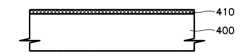
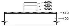
제4 실시예에서는 본 발명에 의한 금속 산화막, 즉 알루미늄 산화막이 MFMIS(metal ferroelectric metal insulator silicon) 트랜지스터 또는 MFIS(metal ferroelectric insulator silicon) 트랜지스터의 절연막으로 사용된다. 도 3을 참고하면, 반도체 기판(400)상에 절연막(410)이 형성되어 있고 절연막위에 제1 금속막 패턴-고유전체막 패턴-제2 금속막 패턴(420A-430A-440A)으로 이루어진 전극이 형성되어 있다. 절연막(410)은 알루미늄 산화막으로 이루어지는 것이 바람직하다. 알루미늄 산화막의 두께는 10Å 내지 250Å인 것이 바람직하며, 더욱 바람직하기로는 10Å 내지 100Å 두께를 지닌다. 알루미늄 산화막은 250∼450℃에서, 더욱 바람직하기로는 350℃에서 증착된 것이 사용된다. 특히 ALD(atomic layer deposition)방식으로 증착되어 균일도와 단차 피복력이 향상된 알루미늄 산화막을 사용한다. 그리고 증착후 산소 분위기하에서 250∼600℃로, 바람직하기로는 400℃∼500℃로 열처리되어 안정화된 막질을 지닌 알루미늄 산화막을 이용한다.In the fourth embodiment, a metal oxide film according to the present invention, that is, an aluminum oxide film, is used as an insulating film of a metal ferroelectric metal insulator silicon (MFMIS) transistor or a metal ferroelectric insulator silicon (MFIS) transistor. Referring to FIG. 3, an insulating
절연막으로 사용되는 알루미늄 산화막(410)은 박막으로 형성될 수 있으며, 박막 상태에서도 우수한 장벽 특성을 나타낸다. 따라서 반도체 기판의 실리콘 원자가 제1 금속막 패턴(420A)으로 확산되는 것을 방지할 수 있다. 따라서 MFMIS 트랜지스터 또는 MFIS 트랜지스터의 게이트 절연막으로 본 발명에 따른 알루미늄 산화막을 형성하면 트랜지스터의 특성이 향상된다.The
집적 회로 장치의 제조 방법Method of manufacturing integrated circuit device
도 5 내지 도 7에는 본 발명의 제1 실시예에 따른 집적 회로 장치의 제조방법을 설명하기 위한 제조 공정 중간 단계 구조물들의 단면도들이 도시되어 있다.5 through 7 are cross-sectional views of structures in an intermediate stage of a manufacturing process for explaining a method of manufacturing an integrated circuit device according to a first embodiment of the present invention.
도 5를 참고하면, 반도체 기판(100) 상에 LOCOS 공정등을 통하여 소자 분리막(102)을 형성한다. 소자 분리막에 의해 정의된 활성 영역상에 게이트 전극(104) 및 측벽 스페이서(104)를 차례대로 형성한다. 다음에 상기 게이트 전극(104)과 측벽 스페이서(104) 및 소정의 마스크 패턴을 이온 주입 마스크로 이용하여 불순물 이온을 주입하여 불순물 영역(108)을 형성하여 트랜지스터를 완성한다. 트랜지스터가 형성된 기판 전면에 층간 절연막(110)을 형성하여 각 트랜지스터를 절연시키고 평탄화한다. 다음에 층간 절연막(110)을 패터닝하여 불순물 영역(108)을 노출시키는 콘택홀을 형성한다. 이어서 다결정 실리콘을 기판 전면에 도포하여 상기 콘택홀을 매립하는 콘택 플러그(112)를 형성한다. 콘택 플러그(112)가 형성된 층간 절연막(110)위에 장벽막, 하부 전극용 도전막, 고유전체막 및 상부 전극용 도전막을 차례대로 형성한 후, 소정의 패턴으로 패터닝하여 상부 전극 패턴(120), 고유전율의 강유전체막 패턴(118), 하부 전극 패턴(116) 및 장벽막 패턴(114)으로 이루어진 커패시터를 완성한다.Referring to FIG. 5, the
장벽막 패턴(114)은 반도체 기판(100) 및 콘택 플러그(112)등에 도우프되어 있는 불순물 또는 실리콘 원자가 하부 전극 패턴(116)으로 확산되는 것을 방지하기 위하여 형성한다. TiN, TiSiN, TaN, TaSiN, TiAlN, TaAlN 또는 RuO2등을 이용하여 장벽막을 형성할 수 있으나, 본 실시예에서는 박막 상태에서도 우수한 장벽 특성을 나타내는 알루미늄 산화막과 TiN, TiSiN, TaN, TaSiN, TiAlN, TaAlN 또는 RuO2등과의 복합 이중막을 사용하여 형성한다. 도5 에서는 장벽막(114)이 콘택 플러그(112) 상부에 형성되어 있으나 도5 에 도시된 집적 회로 장치보다 집적도가 낮은 경우에는 콘택 플러그(112) 상부에 커패시터가 형성되지 않으므로 이 경우 장벽막(114)은 도3 에 도시되어 있는 경우와 마찬가지로 접착층으로서 기능을 주로 수행하게 된다.The
하부 전극 패턴(116) 및 상부 전극 패턴(120)은 백금(Pt), 루테늄(Ru) 이리듐(Ir) 또는 팔라듐(Pd)과 같은 내산화성 금속 물질을 사용하여 형성한다. 고유전율의 강유전체막 패턴(112)은 PZT(Pb(Zr1-xTix)O3), BaTiO3,PbTiO3또는 SrTiO3(STO)로 형성된다.The
도 6을 참고하면, 상기 커패시터가 형성된 결과물 전면에 완충막(122)을 형성한다. 완충막(122)은 600℃ 이하의 저온 처리로 안정화되는 금속 산화막으로 형성되는 것이 바람직하다. 따라서 금속 산화막으로는 알루미늄 산화막을 사용하는 것이 바람직하다.Referring to FIG. 6, the
알루미늄 산화막은 ALD(atomic layer deposition)방식으로 증착하는 것이 균일도 및 단차 피복력 향상 측면에서 바람직하다. 먼저 250∼450℃로 온도가 유지되는 반응기내로 알루미늄 소오스를 주입한 후, 1∼30초의 정화(purge) 시간을 통해 반응기내를 비활성 상태로 만든 후, 산소 소오스롤 주입하여 알루미늄 산화막을 형성한다. 알루미늄 산화막은 40Å 내지 300Å 두께로 바람직하기로는 80Å 내지 200Å 두께로 형성한다. 증착된 알루미늄 산화막은 후속 공정인 어닐링에 의해 막질이 안정화된다. 어닐링은 산소 분위기하에서 250∼600℃로, 바람직하기로는 400 ∼500 ℃로 알루미늄 산화막을 열처리한다.It is preferable to deposit the aluminum oxide film by ALD (atomic layer deposition) method from the viewpoint of improving uniformity and step coverage. First, an aluminum source is injected into a reactor maintained at a temperature of 250 to 450 ° C., and then the reactor is inactivated through a purge time of 1 to 30 seconds, and then an oxygen source is injected to form an aluminum oxide film. . The aluminum oxide film is formed in a thickness of 40 kPa to 300 kPa, preferably of 80 kPa to 200 kPa. The deposited aluminum oxide film is stabilized in film quality by annealing, which is a subsequent process. Annealing heat-treats an aluminum oxide film at 250-600 degreeC in oxygen atmosphere, Preferably it is 400-500 degreeC.
도 6을 참고하면, 안정화된 금속 산화막(122) 위에 절연막(124)을 형성한다. 절연막(124)은 실리콘을 포함하는 산화막을 이용하여 형성한다. 따라서 실리콘 산화막, BPSG 및 PSG로 이루어진 그룹에서 선택된 어느 하나로 형성되는 것이 바람직하다.Referring to FIG. 6, an insulating
본 발명에 따르면, 하부 전극 패턴(116), 고유전체막 패턴(118) 및 상부 전극 패턴(120)으로 이루어진 커패시터와 상기 절연막(124) 사이에 형성되는 금속 산화막(122)은 600℃ 이하의 저온 열처리만으로도 안정한 막질을 형성한다. 따라서 고온 공정을 요구하지 않으므로 집적 회로의 고집적화에 유리하며, 콘택 플러그(112)와 하부 전극 패턴(116)사이의 장벽막(114)도 후속 열처리 공정에 의해 변성되지 않는다. 따라서 전반적인 커패시터의 특성을 양호하게 형성할 수 있다.According to the present invention, the
도 8 내지 도 11에는 본 발명의 제2 실시예에 의한 집적 회로 장치의 제조 방법을 설명하기 위한 제조 공정 중간 단계 구조물들의 단면도들이 도시되어 있다.8 to 11 are cross-sectional views of structures in an intermediate stage of a manufacturing process for explaining a method of manufacturing an integrated circuit device according to a second embodiment of the present invention.
제2 실시예에 의한 집적 회로 장치의 제조 방법은 도 5 내지 도 7에 도시된 제1 실시예에 의한 집적 회로 장치의 제조 방법과 달리, 도8에 도시되어 있는 바와 같이 제1완충막 패턴(114)과 하부 전극 패턴(116)을 먼저 형성한다는 점에 있어서 차이가 있다. 이어서 도 9에 도시되어 있는 바와 같이 고유전율의 상유전체막(118), 예컨대 BST막 및 상부 전극(120)을 차례대로 형성한 후, 소정의 패턴으로 패터닝하여 커패시터를 완성한다.The manufacturing method of the integrated circuit device according to the second embodiment is different from the manufacturing method of the integrated circuit device according to the first embodiment shown in FIGS. 5 to 7, as shown in FIG. 8. There is a difference in forming the 114 and the
다음에 도 10에 도시되어 있는 바와 같이 완충막(122)을 형성한 후, 산소 분위기하에서 어닐링을 하여 막질을 안정화시키는 공정은 제1 실시예와 동일하게 진행한다. 어닐링 공정에 의해 완충막(122)의 막질이 안정화될 뿐만 아니라 고유전율의 강유전체막(118)의 유전율 또한 증가하므로 커패시터의 커패시턴스도 증가하는 장점이 있다. 그리고 완충막(122)을 구성하는 알루미늄 산화막은 산소 확산 억제 능력이 우수하다. 따라서 어닐링 공정시 장벽막(114)의 산화를 방지하기 때문에 하부 전극 패턴(116)과 콘택 플러그(112) 간의 접촉 저항 증가를 방지한다. 이후 도 11에 도시되어 있는 바와 같이 절연막(124)를 형성하는 공정은 제1 실시예와 동일하게 진행된다.Next, as shown in FIG. 10, after the
도 12 내지 도 13 에는 본 발명의 제4 실시예에 의한 MFMIS 트랜지스터의 제조방법을 설명하기 위한 제조 공정 중간 단계 구조물들의 단면도들이 도시되어 있다.12 to 13 are cross-sectional views of structures in an intermediate stage of a manufacturing process for explaining a method of manufacturing an MFMIS transistor according to a fourth embodiment of the present invention.
도 12를 참고하면, 반도체 기판(400)상에 절연막(410)을 형성한다. 절연막(410)은 600℃ 이하의 저온 처리로 안정화되는 금속 산화막으로 형성한다. 따라서 알루미늄 산화막이 사용된다. 알루미늄 산화막은 ALD(atomic layer deposition)방식으로 증착하는 것이 균일도 및 단차 피복력 향상 측면에서 바람직하다. 먼저 250∼450℃로 온도가 유지되는 반응기내로 알루미늄 소오스를 주입한 후, 1∼30초의 정화 시간을 통해 반응기내를 비활성 상태로 만든 후, 산소 소오스롤 주입하여 알루미늄 산화막을 형성한다. 알루미늄 산화막은 10Å 내지 250Å 두께로 형성하는 것이 바람직하다. 알루미늄 산화막을 증착한 후, 산소 분위기하에서 250∼600℃로, 바람직하기로는 400∼500℃로 알루미늄 산화막을 열처리하여 알루미늄 산화막으로 이루어진 절연막(410)을 완성한다. 이 때 알루미늄 산화막의 열처리는 하부 실리콘 기판(400)의 산화를 억제하기 위하여 질소, 암모니아, 아르곤 또는 진공 분위기에서 열처리할 수도 있다.Referring to FIG. 12, an insulating
도 13을 참고하면, 절연막(410)위에 제1 금속막(420), 고유전체막(430) 및 제2 금속막(440)을 차례대로 형성한다. 제1 금속막(420) 및 제2 금속막(440)은 백금(Pt), 루테늄(Ru) 이리듐(Ir) 또는 팔라듐(Pd)과 같은 내산화성 금속 물질을 사용하여 형성하고, 고유전체막(430)은 PZT(Pb(Zr1-xTix)O3), BaTiO3, PbTiO3, SrTiO3(STO) 또는 (Ba,Sr)TiO3(BST)을 사용하여 형성한다.Referring to FIG. 13, a
도 14를 참고하면, 상기 제2 금속막(440), 고유전체막(430) 및 제1 금속막(420)을 차례대로 패터닝하여 제2 금속막 패턴(440A), 고유전체막 패턴(430A) 및 제1 금속막 패턴(420A)으로 이루어진 전극을 형성하여 MFMIS구조를 완성한다.Referring to FIG. 14, the
본 발명에 따르면, 저온 공정으로 박막의 알루미늄 산화막을 MFMIS 구조의 절연막(410)으로 사용한다. 특히 알루미늄 산화막(410)은 박막 상태에서도 우수한 장벽 특성을 나타낸다. 따라서 반도체 기판(400)의 실리콘 원자가 제1 금속막 패턴(420A)으로 확산되는 것을 방지할 수 있다. 또 알루미늄 산화막(410)은 산소 확산 억제 능력이 우수하므로 후속 열처리 공정중에 산소가 확산하여 실리콘 기판(400)이 산화를 방지할 수 있다. 따라서 실리콘 기판(400)의 유전율이 감소하는 것을 억제할 수 있다. 또한 알루미늄 산화막(410)은 유전율이 8∼10 정도로 실리콘 산화막의 유전율인 4에 비해 유전율이 크다. 따라서 MFIS 또는 MFMIS의 고유전체막에 전압이 많이 인가되도록 할 수 있으므로 MFIS 또는 MFMIS의 절연막으로서 적합하다.According to the present invention, a thin aluminum oxide film is used as the insulating
본 발명은 하기의 실험예를 참고로 더욱 상세히 설명되며, 이 실험예가 본 발명을 제한하려는 것은 아니다.The present invention is described in more detail with reference to the following experimental examples, which are not intended to limit the present invention.
알루미늄 산화막 증착 직후의 커패시터 분극 특성Capacitor Polarization Characteristics Immediately after Aluminum Oxide Deposition
도 2에 도시되어 있는 집적 회로 장치와 같이 기판상에 장벽막으로 티타늄 산화막을, 하부 전극으로 백금막을, 유전체막으로 PZT막을 상부 전극으로 백금막을 증착하였다. 상부 전극 및 유전체막만 패터닝한 후, 하기 표1과 같은 조건으로 알루미늄 산화막을 증착하였다.As in the integrated circuit device shown in Fig. 2, a titanium oxide film was used as a barrier film, a platinum film was used as a lower electrode, a PZT film was used as a dielectric film, and a platinum film was used as an upper electrode. After patterning only the upper electrode and the dielectric film, an aluminum oxide film was deposited under the conditions shown in Table 1 below.
알루미늄 산화막 증착 직후 커패시터의 분극 특성을 측정하여 그 결과를 도15a 내지 도 15c 에 도시하였다. 도 15a 내지 도 15c 로부터 알 수 있듯이, 알루미늄 산화막 증착 조건에 상관없이 알루미늄 산화막 증착 직후의 커패시터는 어떠한 분극 특성도 나타내지 않았다.The polarization characteristics of the capacitors were measured immediately after deposition of the aluminum oxide film, and the results are shown in FIGS. 15A to 15C. As can be seen from Figs. 15A to 15C, the capacitor immediately after the deposition of the aluminum oxide film showed no polarization characteristic regardless of the aluminum oxide deposition conditions.
알루미늄 산화막 어닐링후의 커패시터 분극 특성Capacitor Polarization Characteristics after Aluminum Oxide Annealing
커패시터의 상부 전극 패턴과 고유전체막 패턴까지는 앞의 실험예와 동일하게 형성한 후, 하기 표2와 같이 알루미늄 산화막을 증착하였다. 이어서 450℃ 산소 분위기하에서 30분간 어닐링한 후, 커패시터의 분극 특성을 각각 측정하였다.After forming the upper electrode pattern and the high dielectric film pattern of the capacitor in the same manner as in the previous experimental example, an aluminum oxide film was deposited as shown in Table 2 below. Subsequently, after annealing for 30 minutes in 450 degreeC oxygen atmosphere, the polarization characteristic of the capacitor was measured, respectively.
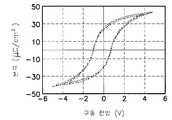
알루미늄 산화막의 두께가 100Å일 때의 결과가 도 16a 에, 300Å일 때의 결과가 도 16b 에 도시되어 있다. 알루미늄 산화막을 100Å두께로 형성한 후, 어닐링 처리전의 결과를 나타내는 도 15c 와 어닐링 처리후의 결과를 나타내는 도 16a를 비교해보면, 어닐링전에는 분극 특성이 나타나지 않았으나 어닐링후에는 분극 특성이 완전히 회복되었음을 알 수 있다. 또한, 도 16b 로부터 알루미늄 산화막의 두께가 300Å일 때도 분극 특성이 완전히 회복되었음을 알 수 있다.The result when the thickness of the aluminum oxide film is 100 mW is shown in Fig. 16A and the result when the aluminum oxide film is 300 mV is shown in Fig. 16B. After the aluminum oxide film was formed to have a thickness of 100 mV, comparing FIG. 15C showing the result after the annealing treatment with FIG. 16A showing the result after the annealing treatment, it was found that the polarization characteristics were not recovered before the annealing, but the polarization characteristics were completely recovered after the annealing. . In addition, it can be seen from FIG. 16B that the polarization characteristic was completely recovered even when the thickness of the aluminum oxide film was 300 GPa.
알루미늄 산화막 어닐링후의 커패시터 잔류 분극과 누설 전류 특성Capacitor Residual Polarization and Leakage Current Characteristics after Aluminum Oxide Annealing
하기 표3 과 같이 알루미늄 산화막 증착 조건과 어닐링 조건을 설정하여 알루미늄 산화막을 형성하고 어닐링 처리를 한 후, 각각에 대하여 잔류 분극 특성과 누설 전류 특성을 측정하였다. 이때 각 조건별로 샘플의 수는 6개로 하였다.After the aluminum oxide film deposition conditions and annealing conditions were set as shown in Table 3 below, the aluminum oxide film was formed and annealed, and then the residual polarization characteristics and the leakage current characteristics were measured. At this time, the number of samples for each condition was six.
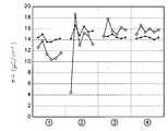
표 3 에 따라 알루미늄 산화막을 형성한 후 잔류 분극을 측정한 결과가 도17 에 도시되어 있다. 도 17의 결과로부터 알 수 있듯이, 대부분의 경우 어닐링 처리를 거친후에는 잔류 분극값이 거의 일정하게 나타남을 알 수 있다.The results of measuring the residual polarization after forming the aluminum oxide film according to Table 3 are shown in FIG. As can be seen from the result of FIG. 17, in most cases, the residual polarization value is almost constant after the annealing treatment.
그러나 ③의 경우와 같이 알루미늄 증착 온도를 250℃로 낮게 한 경우, 잔류 분극 값이 일정하지 않았다. 그 이유는 증착 온도가 낮은 경우 알루미늄 산화막 내에 불순물이 포함될 가능성이 높기 때문인 것으로 해석된다. 그리고 ⑥의 경우와 같이 정화 시간이 9.9초로 긴 경우에도 잔류 분극 값이 일정하지 않게 나타났다. 그 이유는 알루미늄 단층을 형성한 후, 정화 시간이 길 경우 알루미늄 단층이 PZT와 반응하여 분극 특성의 불안정을 가져오기 때문인 것으로 추측된다. 또 알루미늄 산화막을 80Å 두께로 형성한 ⑦의 경우에도 잔류 분극 값이 불균일하게 나타났다. 그러나 도 16a 와 도 16b에서 알 수 있듯이 알루미늄 산화막의 두께를 100Å과 300Å으로 한 경우에는 분극 특성이 양호한 것으로 보아 알루미늄 산화막의 두께와 잔류 분극 간의 상관관계는 없는 것으로 판단된다.However, when the aluminum deposition temperature was lowered to 250 ° C. as in the case of ③, the residual polarization value was not constant. The reason for this is interpreted as a high possibility that impurities are included in the aluminum oxide film when the deposition temperature is low. And as in the case of ⑥, even when the purification time is long as 9.9 seconds, the residual polarization value was not constant. The reason for this is presumably because, after forming the aluminum monolayer, when the purification time is long, the aluminum monolayer reacts with PZT, resulting in instability in polarization characteristics. In the case of ⑦ in which the aluminum oxide film was formed to a thickness of 80 Å, the residual polarization value was uneven. However, as can be seen from FIGS. 16A and 16B, when the thickness of the aluminum oxide film is 100 kPa and 300 kPa, the polarization characteristic is considered to be good, and thus there is no correlation between the thickness of the aluminum oxide film and the residual polarization.
각 샘플에 대한 누설 전류 특성은 도18 에 도시되어 있다. 도18 으로부터 알수 있듯이, 알루미늄 산화막 증착 조건에 상관없이 산소 분위기하에서 450℃로 30분간 어닐링한 후에는 모두 10-9(A/1.4×10-4㎛2)이하의 누설전류를 나타내었다.Leakage current characteristics for each sample are shown in FIG. As can be seen from Fig. 18, after annealing at 450 DEG C for 30 minutes in an oxygen atmosphere irrespective of the deposition conditions of aluminum oxide films, leakage currents of 10-9 (A / 1.4 x 10⁻⁴ mu m2 ) or less were all exhibited.
비교예로서 종래 기술에서 언급한 미국 특허 번호 제 5,212,620에 개시되어 있는 방법에 따라 티타늄 산화막을 증착한 후, 어닐링 온도만 650℃, 550℃ 및 450℃로 각각 다르게한 후, 커패시터의 누설전류를 측정하였다. 그 결과를 하기 표4 에 나타내었다.As a comparative example, after depositing a titanium oxide film according to the method disclosed in U.S. Patent No. 5,212,620 mentioned in the prior art, after varying only the annealing temperature to 650 ° C, 550 ° C and 450 ° C, the leakage current of the capacitor was measured. It was. The results are shown in Table 4 below.
종래 기술에 따라 티타늄 산화막을 완충막으로 형성하는 경우, 650℃로 열처리하는 경우에도 누설 전류가 10-6A/㎠ 정도이고, 열처리 온도가 낮아지면 낮아질수록 누설 전류 값이 증가하여 450℃로 열처리하는 경우에는 누설 전류가 10-4A/㎠ 로 매우 높게 나타나는 것을 알 수 있다.According to the prior art, when the titanium oxide film is formed as a buffer film, the leakage current is about 10−6 A /
즉, 종래 기술에 따른 티타늄 산화막은 저온 공정을 요구하는 고집적화된 집적 회로 장치의 제조에 부적합한 것을 알 수 있다. 반면, 본 발명에 따른 알루미늄 산화막은 저온의 어닐링 처리만으로도 그 막질이 안정화될 수 있어서, 커패시터와 콘택 플러그 사이에 형성되어 있는 장벽막이 고온 처리에 변성되는 것을 방지할 수 있다. 그러므로 본 발명에 따른 알루미늄 산화막은 저온 공정을 필요로 하는 고집적화된 집적 회로 장치의 제조에 적합하다.That is, it can be seen that the titanium oxide film according to the prior art is unsuitable for manufacturing a highly integrated integrated circuit device requiring a low temperature process. On the other hand, the aluminum oxide film according to the present invention can be stabilized only by the low temperature annealing treatment, thereby preventing the barrier film formed between the capacitor and the contact plug from being denatured in the high temperature treatment. Therefore, the aluminum oxide film according to the present invention is suitable for the fabrication of highly integrated integrated circuit devices requiring low temperature processes.
절연막 증착 후의 커패시터 잔류 분극과 누설 전류 특성Capacitor Residual Polarization and Leakage Current Characteristics after Insulator Film Deposition
하기 표 5와 같이 알루미늄 산화막을 증착하고 어닐링한 후 결과물 전면에 실리콘 산화막을 형성하였다. 실리콘 산화막은 ECR-CVD 방법으로 증착하였다.After depositing and annealing an aluminum oxide film as shown in Table 5, a silicon oxide film was formed on the entire surface of the resultant. The silicon oxide film was deposited by the ECR-CVD method.
각각의 표본에 대하여 잔류 분극 특성을 측정한 그래프가 도 14 에 도시되어 있다. -●-로 표시된 그래프는 실리콘 산화막 증착 전에 측정한 잔류 분극값을 나타내고 -○-로 표시된 그래프는 실리콘 산화막 증착후에 측정한 잔류 분극값을 나타낸다.A graph measuring residual polarization characteristics for each sample is shown in FIG. 14. The graph marked by-●-represents the residual polarization value measured before the deposition of the silicon oxide film, and the graph marked with-○-represents the residual polarization value measured after the deposition of the silicon oxide film.
도 19에 따르면, 알루미늄 산화막의 두께를 40Å으로 형성한 경우(①), 실리콘 산화막 증착후의 잔류 분극 특성이 증착전에 비해 열화되었음을 알 수 있다. 그리고 알루미늄 산화막을 250℃에서 60Å 두께로 형성한 경우(②)에도 잔류 분극 특성이 불균일하게 나타났음을 알 수 있다. 반면 60Å 두께의 알루미늄 산화막을 350℃에서 증착한 경우 정화시간에 관계 없이 잔류 분극 특성이 실리콘 산화막 증착후에 더 양호해졌음을 알 수 있다.According to Fig. 19, when the thickness of the aluminum oxide film is formed to be 40 kW (1), it can be seen that the residual polarization characteristics after the deposition of the silicon oxide film are degraded compared to before the deposition. In addition, it can be seen that even when the aluminum oxide film was formed to have a thickness of 60 kPa at 250 ° C. (②), residual polarization characteristics appeared unevenly. On the other hand, when the 60 nm thick aluminum oxide film was deposited at 350 ° C., the residual polarization property was improved after deposition of the silicon oxide film regardless of the purification time.
또, 각각의 표본에 대하여 누설 전류 특성을 측정한 그래프가 도 20에 도시되어 있다. -●-로 표시된 그래프는 실리콘 산화막 증착 전에 측정한 누설 전류값을 나타내고 -○-로 표시된 그래프는 실리콘 산화막 증착후에 측정한 누설 전류값을 나타낸다. 도 20 으로부터 알루미늄 산화막 증착전에는 누설 전류 값이 높았던 경우(①, ②)에도 실리콘 산화막을 증착한 후에는 누설 전류 값이 χ×10-10(A/1.4×10-4㎛2) 정도로 낮아졌음을 알 수 있다.Moreover, the graph which measured the leakage current characteristic about each sample is shown in FIG. The graph marked with-●-represents the leakage current value measured before the deposition of the silicon oxide film, and the graph marked with-○-represents the leakage current value measured after the deposition of the silicon oxide film. From Fig. 20, even when the leakage current value was high (1, 2) before deposition of the aluminum oxide film, after the deposition of the silicon oxide film, the leakage current value was lowered to χ 10-10 (A / 1.4 x 10⁻⁴ μm2 ). Able to know.
NHNH33플라즈마 처리와 잔류 분극 특성간의 관계 측정Measurement of the relationship between plasma treatment and residual polarization characteristics
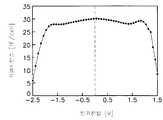
알루미늄 산화막이 후속 공정에서 발생하는 수소의 침투에 대한 확산 방지막으로서 기능을 충분히 수행할 수 있는지 여부를 알아보기 위하여, 알루미늄 산화막을 20Å 과 80Å으로 각각 형성한 후, NH3플라즈마 처리를 하였다. NH3플라즈마 처리는 NH3를 10mTorr압력과 1200W의 마이크로파 동력하에서 80sccm으로 플로우시켰다. NH3플로우 전과 후의 분극 특성을 각각 측정하여 도 21에 도시하였다.In order to find out whether the aluminum oxide film can function sufficiently as a diffusion barrier against the penetration of hydrogen generated in a subsequent step, the aluminum oxide film was formed at 20 kPa and 80 kPa, respectively, and then subjected to NH3 plasma treatment. NH3 plasma treatment flowed NH3 at 80 sccm under 10 mTorr pressure and 1200 W microwave power. Polarization characteristics before and after the NH3 flow were measured and shown in FIG. 21.
도 21은 알루미늄 산화막의 두께가 80Å일 때의 분극 특성을 나타내는 그래프로서 NH3플로우 전과 후의 분극 특성이 전혀 변화가 없었음을 알 수 있다. 반면 알루미늄 산화막의 두께가 20Å일 때에는 웨이퍼 전면에서 리프팅이 발생하여 커패시터 특성을 측정할 수 없었다.FIG. 21 is a graph showing the polarization characteristics when the thickness of the aluminum oxide film is 80 kPa, and it can be seen that the polarization characteristics before and after the NH3 flow did not change at all. On the other hand, when the thickness of the aluminum oxide film was 20 kW, the lifting occurred on the front surface of the wafer, and thus the capacitor characteristics could not be measured.
알루미늄 산화막의 두께와 리프팅 발생간의 관계Relationship between aluminum oxide film thickness and lifting occurrence
알루미늄 산화막의 두께와 리프팅 발생간에는 어떠한 관계가 있는지 알아보기 위하여 하기 표6과 같은 조건으로 알루미늄 산화막을 형성하였다. 각 조건별로 리프팅이 발생하였는지 여부를 ○,×로 표시하였다. 표6으로부터 알루미늄 산화막의 두께가 20Å일 때와 300Å 이상일 때에는 실리콘 산화막의 형성여부와 관계없이 450℃에서 30분간 어닐링 후에 리프팅이 발생하였음을 알 수 있다. 그리고 100Å일 때에도 어닐링 직후에는 리프팅이 발생하지 않았으나, 실리콘 산화막 형성후에는 리프팅이 발생하는 것으로 보아 리프팅 관점에서 보면 알루미늄 산화막의 적정 두께는 40Å 내지 80Å임을 알 수 있다. 또 알루미늄 산화막이 적정 두께인 60Å으로 형성될지라도 증착 온도가 250℃ 인 경우와 정화 시간이 9.9초인 경우에도 리프팅이 발생하였음을 알 수 있다. 그러므로 리프팅이 발생하지 않도록 하려면 알루미늄 산화막의 두께는 40∼80Å 으로 증착 온도는 300℃ 내지 400℃ 정화 시간은 9.9 초 이하 바람직하기로는 3.3 초 이하임을 알 수 있다.In order to examine the relationship between the thickness of the aluminum oxide film and the lifting occurrence, the aluminum oxide film was formed under the conditions shown in Table 6 below. Whether or not lifting occurred for each condition is indicated by ○, ×. It can be seen from Table 6 that the lifting occurred after annealing at 450 ° C. for 30 minutes regardless of the formation of the silicon oxide film when the thickness of the aluminum oxide film was 20 GPa and 300 GPa or more. In addition, even when 100 kW, the lifting did not occur immediately after the annealing, but after the silicon oxide film was formed, the lifting occurred. Therefore, it can be seen that the optimum thickness of the aluminum oxide film is 40 kPa to 80 kPa from the lifting point of view. In addition, even if the aluminum oxide film was formed to a suitable thickness of 60 kPa, it can be seen that the lifting occurred even when the deposition temperature was 250 ° C. and the purification time was 9.9 seconds. Therefore, in order to prevent the lifting, it can be seen that the thickness of the aluminum oxide film is 40 to 80 kPa, the deposition temperature is 300 ° C to 400 ° C, and the purification time is preferably 9.9 seconds or less, preferably 3.3 seconds or less.
이상에서 설명한 결과는 하부 전극을 패터닝하지 않은 상태로 형성한 다음 표 6에 도시된 조건으로 처리한 후 리프팅 여부를 관찰한 것이다. 반면 하부 전극을 패터닝한 후에 알루미늄 산화막을 증착한 경우에는 알루미늄 산화막이 100Å이상 두께로 형성된 경우에도 리프팅이 발생하지 않았다. 이는 하부 전극이 기판 전면에 형성되어 있을 때는 스트레스에 의한 리프팅 여유도(lifting margin)가 적으나 하부전극이 패터닝된 상태에서는 하부 전극 패턴과의 스트레스가 감소하므로 리프팅 억제 여유도가 증가하기 때문이다.The result described above was formed after the lower electrode was not patterned, and then treated under the conditions shown in Table 6, and then examined for lifting. On the other hand, when the aluminum oxide film was deposited after the lower electrode was patterned, no lifting occurred even when the aluminum oxide film was formed to a thickness of 100 GPa or more. This is because when the lower electrode is formed on the front surface of the substrate, the lifting margin due to stress is small, but when the lower electrode is patterned, the stress with the lower electrode pattern decreases, so the lifting suppression margin increases.
알루미늄 산화막 형성과 BST 커패시터 특성간의 관계Relationship between aluminum oxide formation and BST capacitor characteristics
이상의 실험예는 고유전율의 강유전체막(PZT)를 사용한 커패시터의 특성을 측정한 결과를 나타낸 것이다. 이번에는 고유전율의 상유전체막인 BST막을 포함하는 커패시터에 알루미늄 산화막을 형성할 경우 커패시터의 특성에 어떤 영향을 미치는지 알아보기 위하여 다음과 같이 실시하였다. 장벽막으로 TaSiN을 형성하고 그 위에 BST막을 포함하는 커패시터를 형성하였다. 다음에 BST 커패시터위에 100Å 두께의 알루미늄 산화막을 형성하였다. 알루미늄 산화막을 산소분위기 600℃에서 10분간 어닐링한 후, BST 커패시터의 커패시턴스와 누설 전류를 측정하고 그 결과를 도 22와 도 21에 도시하였다. 도 22와 도 23에 도시되어 있는 바와 같이, BST 커패시터의 커패시터는 약 30fF/cell이었고 누설 전류는 2V에서 5×10-16A/cell 이었다. 이는 알루미늄 산화막의 어닐링 공정에 의해 BST의 유전율이 향상되었기 때문에 커패시턴스가 증가된 것으로 해석된다. 또, 알루미늄 산화막이 산소의 확산 방지막으로 작용하므로 장벽막인 TaSiN이 어닐링 공정시 산화되지 않아서 커패시터의 접촉 저항 증가가 방지되었기 때문인 것으로 해석된다.The above experimental example shows the result of measuring the characteristics of a capacitor using a ferroelectric film (PZT) having a high dielectric constant. This time, the aluminum oxide film was formed on the capacitor including the BST film, which is a high dielectric constant dielectric film, to investigate the effect on the characteristics of the capacitor. TaSiN was formed as a barrier film, and a capacitor including a BST film was formed thereon. Next, an aluminum oxide film having a thickness of 100 Å was formed on the BST capacitor. After annealing the aluminum oxide film at an oxygen atmosphere of 600 ° C. for 10 minutes, the capacitance and leakage current of the BST capacitor were measured and the results are shown in FIGS. 22 and 21. As shown in FIGS. 22 and 23, the capacitor of the BST capacitor was about 30 fF / cell and the leakage current was 5 × 10⁻¹⁶ A / cell at 2V. It is interpreted that the capacitance is increased because the dielectric constant of the BST is improved by the annealing process of the aluminum oxide film. In addition, since the aluminum oxide film acts as a diffusion preventing film of oxygen, it is interpreted that the barrier film TaSiN is not oxidized during the annealing process, thereby preventing an increase in the contact resistance of the capacitor.
도면 및 상세한 설명에서 본 발명의 바람직한 실시예가 기술되었고, 특정 용어가 사용되었으나, 이는 이하의 청구범위에 개시되어 있는 발명의 범주로 이를 제한하고자 하는 목적이 아니라 기술적인 개념에서 사용된 것이다. 따라서 본 발명은 상기 실시예에 한정되지 않고 당업자의 수준에서 그 변형 및 개량이 가능하다.While the preferred embodiments of the invention have been described in the drawings and the description, specific terms have been used, which are used in technical concepts rather than for the purpose of limiting the scope of the invention as set forth in the claims below. Therefore, the present invention is not limited to the above embodiments, and modifications and improvements are possible at the level of those skilled in the art.
이상에서 설명한 바와 같이, 본 발명에 따른 완충막은 600℃ 이하의 저온처리만으로도 안정화되는 금속 산화막, 예컨대 알루미늄 산화막으로 구성된다. 일반적으로 집적 회로 장치를 고집적화시키기 위해서는 600℃ 이하로 제조 공정을 저온화시킬 것이 요구된다. 따라서 집적 회로 장치의 완충막으로서 본 발명에 따른 완충막을 사용하면 집적 회로 장치를 용이하게 고집적화할 수 있다. 또한 본 발명에 따른 완충막은 얇게 형성되더라도 완충막 기능을 충분히 달성할 수 있으며, ALD(atomic layered deposition)방식으로 형성되므로 균일도 및 단차 피복력이 뛰어난 장점이 있다. 따라서 본 발명에 따른 완충막을 고유전체막을 포함하는 커패시터와 절연막간의 완충막으로서 사용하면 커패시터의 분극 특성이 양호해지고 누설 전류의 발생도 감소시킬 수 있다. 그리고 본 발명에 따른 완충막은 장벽 특성이 양호하므로 MFMIS의 절연막으로서 사용하면 실리콘 기판의 실리콘 원자가 금속층으로 확산되는 것을 효율적으로 방지할 수 있다.As described above, the buffer film according to the present invention is composed of a metal oxide film, for example, an aluminum oxide film, which is stabilized only by a low temperature treatment of 600 ° C. or less. In general, in order to highly integrate integrated circuit devices, it is required to lower the manufacturing process to 600 ° C or lower. Therefore, when the buffer film according to the present invention is used as the buffer film of the integrated circuit device, the integrated circuit device can be easily integrated. In addition, the buffer film according to the present invention can achieve a sufficient buffer film function even if it is formed thin, and is formed by the ALD (atomic layered deposition) method has an advantage of excellent uniformity and step coverage. Therefore, when the buffer film according to the present invention is used as a buffer film between the capacitor including the high dielectric film and the insulating film, the polarization characteristic of the capacitor can be improved and the occurrence of leakage current can be reduced. In addition, since the buffer film according to the present invention has good barrier properties, it is possible to effectively prevent the diffusion of silicon atoms of the silicon substrate into the metal layer when used as an insulating film of MFMIS.
Claims (17)
Translated fromKoreanPriority Applications (3)
| Application Number | Priority Date | Filing Date | Title |
|---|---|---|---|
| KR1019970036558AKR100269306B1 (en) | 1997-07-31 | 1997-07-31 | Integrate circuit device having buffer layer containing metal oxide stabilized by low temperature treatment and fabricating method thereof |
| JP10055558AJPH1154718A (en) | 1997-07-31 | 1998-03-06 | Integrated circuit device having buffer film constituted of metal oxide film which is stabilized by low temperature treatment, and its manufacture |
| US09/127,353US6144060A (en) | 1997-07-31 | 1998-07-31 | Integrated circuit devices having buffer layers therein which contain metal oxide stabilized by heat treatment under low temperature |
Applications Claiming Priority (1)
| Application Number | Priority Date | Filing Date | Title |
|---|---|---|---|
| KR1019970036558AKR100269306B1 (en) | 1997-07-31 | 1997-07-31 | Integrate circuit device having buffer layer containing metal oxide stabilized by low temperature treatment and fabricating method thereof |
Publications (2)
| Publication Number | Publication Date |
|---|---|
| KR19990012976A KR19990012976A (en) | 1999-02-25 |
| KR100269306B1true KR100269306B1 (en) | 2000-10-16 |
Family
ID=19516501
Family Applications (1)
| Application Number | Title | Priority Date | Filing Date |
|---|---|---|---|
| KR1019970036558AExpired - Fee RelatedKR100269306B1 (en) | 1997-07-31 | 1997-07-31 | Integrate circuit device having buffer layer containing metal oxide stabilized by low temperature treatment and fabricating method thereof |
Country Status (3)
| Country | Link |
|---|---|
| US (1) | US6144060A (en) |
| JP (1) | JPH1154718A (en) |
| KR (1) | KR100269306B1 (en) |
Families Citing this family (253)
| Publication number | Priority date | Publication date | Assignee | Title |
|---|---|---|---|---|
| FI119941B (en)* | 1999-10-15 | 2009-05-15 | Asm Int | Process for the preparation of nanolaminates |
| US6586790B2 (en)* | 1998-07-24 | 2003-07-01 | Kabushiki Kaisha Toshiba | Semiconductor device and method for manufacturing the same |
| FI108375B (en)* | 1998-09-11 | 2002-01-15 | Asm Microchemistry Oy | Still for producing insulating oxide thin films |
| US6974766B1 (en) | 1998-10-01 | 2005-12-13 | Applied Materials, Inc. | In situ deposition of a low κ dielectric layer, barrier layer, etch stop, and anti-reflective coating for damascene application |
| JP4501170B2 (en)* | 1999-03-18 | 2010-07-14 | ソニー株式会社 | Semiconductor device and manufacturing method thereof |
| JP2000315778A (en)* | 1999-04-30 | 2000-11-14 | Hitachi Ltd | Semiconductor integrated circuit device and method of manufacturing the same |
| KR100329781B1 (en)* | 1999-06-28 | 2002-03-25 | 박종섭 | Method for forming feram capable of preventing hydrogen diffusion |
| US7060584B1 (en)* | 1999-07-12 | 2006-06-13 | Zilog, Inc. | Process to improve high performance capacitor properties in integrated MOS technology |
| KR100309077B1 (en)* | 1999-07-26 | 2001-11-01 | 윤종용 | Triple metal 1t/1c ferroelectric capacitor and method for fabricating thereof |
| DE19946437A1 (en) | 1999-09-28 | 2001-04-12 | Infineon Technologies Ag | Ferroelectric transistor |
| WO2001029893A1 (en) | 1999-10-15 | 2001-04-26 | Asm America, Inc. | Method for depositing nanolaminate thin films on sensitive surfaces |
| JP3800294B2 (en) | 1999-10-25 | 2006-07-26 | 日本電気株式会社 | Semiconductor device and manufacturing method thereof |
| KR20020063206A (en) | 1999-12-09 | 2002-08-01 | 동경 엘렉트론 주식회사 | METHOD FOR FORMING TiSiN FILM, DIFFUSION PREVENTIVE FILM COMPRISING TiSiN FILM, SEMICONDUCTOR DEVICE AND ITS PRODUCTION METHOD, AND APPARATUS FOR FORMING TiSiN FILM |
| KR100323874B1 (en)* | 1999-12-22 | 2002-02-16 | 박종섭 | Method of forming an aluminum oxide film in a semiconductor device |
| KR100705926B1 (en)* | 1999-12-22 | 2007-04-11 | 주식회사 하이닉스반도체 | Capacitor Manufacturing Method of Semiconductor Device |
| KR100624903B1 (en)* | 1999-12-22 | 2006-09-19 | 주식회사 하이닉스반도체 | Capacitor Manufacturing Method of Semiconductor Device |
| US6548343B1 (en)* | 1999-12-22 | 2003-04-15 | Agilent Technologies Texas Instruments Incorporated | Method of fabricating a ferroelectric memory cell |
| KR100356473B1 (en)* | 1999-12-29 | 2002-10-18 | 주식회사 하이닉스반도체 | Method of forming a aluminum oxide thin film in a semiconductor device |
| US6319766B1 (en) | 2000-02-22 | 2001-11-20 | Applied Materials, Inc. | Method of tantalum nitride deposition by tantalum oxide densification |
| JP3548488B2 (en)* | 2000-03-13 | 2004-07-28 | 沖電気工業株式会社 | Method for manufacturing semiconductor device using ferroelectric substance |
| JP2001308287A (en)* | 2000-04-26 | 2001-11-02 | Sharp Corp | Semiconductor device and manufacturing method thereof |
| US7494927B2 (en) | 2000-05-15 | 2009-02-24 | Asm International N.V. | Method of growing electrical conductors |
| JP5173101B2 (en)* | 2000-05-15 | 2013-03-27 | エイエスエム インターナショナル エヌ.ヴェー. | Integrated circuit manufacturing method |
| KR100402943B1 (en)* | 2000-06-19 | 2003-10-30 | 주식회사 하이닉스반도체 | High dielectric capacitor and a method of manufacturing the same |
| KR100351056B1 (en)* | 2000-06-27 | 2002-09-05 | 삼성전자 주식회사 | Method of manufacturing semiconductor device including step of selectively forming metal oxide layer |
| US6620723B1 (en) | 2000-06-27 | 2003-09-16 | Applied Materials, Inc. | Formation of boride barrier layers using chemisorption techniques |
| US7964505B2 (en) | 2005-01-19 | 2011-06-21 | Applied Materials, Inc. | Atomic layer deposition of tungsten materials |
| US7101795B1 (en) | 2000-06-28 | 2006-09-05 | Applied Materials, Inc. | Method and apparatus for depositing refractory metal layers employing sequential deposition techniques to form a nucleation layer |
| US6551929B1 (en) | 2000-06-28 | 2003-04-22 | Applied Materials, Inc. | Bifurcated deposition process for depositing refractory metal layers employing atomic layer deposition and chemical vapor deposition techniques |
| US7405158B2 (en) | 2000-06-28 | 2008-07-29 | Applied Materials, Inc. | Methods for depositing tungsten layers employing atomic layer deposition techniques |
| US7732327B2 (en) | 2000-06-28 | 2010-06-08 | Applied Materials, Inc. | Vapor deposition of tungsten materials |
| US6592942B1 (en)* | 2000-07-07 | 2003-07-15 | Asm International N.V. | Method for vapour deposition of a film onto a substrate |
| US7112503B1 (en)* | 2000-08-31 | 2006-09-26 | Micron Technology, Inc. | Enhanced surface area capacitor fabrication methods |
| US7217615B1 (en)* | 2000-08-31 | 2007-05-15 | Micron Technology, Inc. | Capacitor fabrication methods including forming a conductive layer |
| US6420230B1 (en)* | 2000-08-31 | 2002-07-16 | Micron Technology, Inc. | Capacitor fabrication methods and capacitor constructions |
| US6465297B1 (en)* | 2000-10-05 | 2002-10-15 | Motorola, Inc. | Method of manufacturing a semiconductor component having a capacitor |
| US6660660B2 (en) | 2000-10-10 | 2003-12-09 | Asm International, Nv. | Methods for making a dielectric stack in an integrated circuit |
| AU2002225761A1 (en)* | 2000-11-30 | 2002-06-11 | Asm America, Inc. | Thin films for magnetic devices |
| KR20020049875A (en) | 2000-12-20 | 2002-06-26 | 윤종용 | Ferroelectric capacitor in semiconductor memory device and method for manufacturing the same |
| US6825447B2 (en) | 2000-12-29 | 2004-11-30 | Applied Materials, Inc. | Apparatus and method for uniform substrate heating and contaminate collection |
| US6998579B2 (en) | 2000-12-29 | 2006-02-14 | Applied Materials, Inc. | Chamber for uniform substrate heating |
| US6765178B2 (en) | 2000-12-29 | 2004-07-20 | Applied Materials, Inc. | Chamber for uniform substrate heating |
| US6951804B2 (en) | 2001-02-02 | 2005-10-04 | Applied Materials, Inc. | Formation of a tantalum-nitride layer |
| US6878206B2 (en) | 2001-07-16 | 2005-04-12 | Applied Materials, Inc. | Lid assembly for a processing system to facilitate sequential deposition techniques |
| US6660126B2 (en) | 2001-03-02 | 2003-12-09 | Applied Materials, Inc. | Lid assembly for a processing system to facilitate sequential deposition techniques |
| US6734020B2 (en) | 2001-03-07 | 2004-05-11 | Applied Materials, Inc. | Valve control system for atomic layer deposition chamber |
| KR100420117B1 (en)* | 2001-03-12 | 2004-03-02 | 삼성전자주식회사 | Semiconductor device having hydrogen diffusion barrier layer and method of fabricating the same |
| DE10116875B4 (en)* | 2001-04-04 | 2006-06-14 | Infineon Technologies Ag | Method for producing an integrated ferroelectric memory |
| KR100389033B1 (en)* | 2001-04-11 | 2003-06-25 | 삼성전자주식회사 | Ferroelectric memory device and fabrication method thereof |
| DE10121132A1 (en)* | 2001-04-30 | 2002-10-31 | Infineon Technologies Ag | Method for producing a metallic or metal-containing layer using a precursor on a silicon- or germanium-containing layer, in particular an electronic component |
| KR100406534B1 (en)* | 2001-05-03 | 2003-11-20 | 주식회사 하이닉스반도체 | Method for fabricating ruthenium thin film |
| US6759081B2 (en)* | 2001-05-11 | 2004-07-06 | Asm International, N.V. | Method of depositing thin films for magnetic heads |
| JP2002353414A (en)* | 2001-05-22 | 2002-12-06 | Oki Electric Ind Co Ltd | Dielectric capacitor and method of manufacturing the same |
| US7037574B2 (en)* | 2001-05-23 | 2006-05-02 | Veeco Instruments, Inc. | Atomic layer deposition for fabricating thin films |
| KR100418581B1 (en)* | 2001-06-12 | 2004-02-11 | 주식회사 하이닉스반도체 | Method of forming memory device |
| KR100422565B1 (en) | 2001-06-12 | 2004-03-12 | 주식회사 하이닉스반도체 | Method of forming a capacitor of a semiconductor device |
| US6849545B2 (en) | 2001-06-20 | 2005-02-01 | Applied Materials, Inc. | System and method to form a composite film stack utilizing sequential deposition techniques |
| CN1290194C (en) | 2001-06-25 | 2006-12-13 | 松下电器产业株式会社 | Capacitance element, semiconductor storage and preparing method thereof |
| US7211144B2 (en) | 2001-07-13 | 2007-05-01 | Applied Materials, Inc. | Pulsed nucleation deposition of tungsten layers |
| US20030198754A1 (en)* | 2001-07-16 | 2003-10-23 | Ming Xi | Aluminum oxide chamber and process |
| US8110489B2 (en) | 2001-07-25 | 2012-02-07 | Applied Materials, Inc. | Process for forming cobalt-containing materials |
| JP2005504885A (en) | 2001-07-25 | 2005-02-17 | アプライド マテリアルズ インコーポレイテッド | Barrier formation using a novel sputter deposition method |
| US20090004850A1 (en) | 2001-07-25 | 2009-01-01 | Seshadri Ganguli | Process for forming cobalt and cobalt silicide materials in tungsten contact applications |
| US9051641B2 (en) | 2001-07-25 | 2015-06-09 | Applied Materials, Inc. | Cobalt deposition on barrier surfaces |
| US20030029715A1 (en) | 2001-07-25 | 2003-02-13 | Applied Materials, Inc. | An Apparatus For Annealing Substrates In Physical Vapor Deposition Systems |
| US7085616B2 (en) | 2001-07-27 | 2006-08-01 | Applied Materials, Inc. | Atomic layer deposition apparatus |
| KR100423906B1 (en)* | 2001-08-08 | 2004-03-22 | 삼성전자주식회사 | Ferroelectric memory device amd method of forming the same |
| US6806145B2 (en) | 2001-08-31 | 2004-10-19 | Asm International, N.V. | Low temperature method of forming a gate stack with a high k layer deposited over an interfacial oxide layer |
| KR100422594B1 (en)* | 2001-09-12 | 2004-03-16 | 주식회사 하이닉스반도체 | Capacitor in semiconductor device and method for fabricating the same |
| US6718126B2 (en) | 2001-09-14 | 2004-04-06 | Applied Materials, Inc. | Apparatus and method for vaporizing solid precursor for CVD or atomic layer deposition |
| US7049226B2 (en)* | 2001-09-26 | 2006-05-23 | Applied Materials, Inc. | Integration of ALD tantalum nitride for copper metallization |
| US6936906B2 (en) | 2001-09-26 | 2005-08-30 | Applied Materials, Inc. | Integration of barrier layer and seed layer |
| US6916398B2 (en) | 2001-10-26 | 2005-07-12 | Applied Materials, Inc. | Gas delivery apparatus and method for atomic layer deposition |
| US7780785B2 (en) | 2001-10-26 | 2010-08-24 | Applied Materials, Inc. | Gas delivery apparatus for atomic layer deposition |
| KR100561839B1 (en) | 2001-11-10 | 2006-03-16 | 삼성전자주식회사 | Ferroelectric Capacitors and Manufacturing Method Thereof |
| US6773507B2 (en) | 2001-12-06 | 2004-08-10 | Applied Materials, Inc. | Apparatus and method for fast-cycle atomic layer deposition |
| US7081271B2 (en) | 2001-12-07 | 2006-07-25 | Applied Materials, Inc. | Cyclical deposition of refractory metal silicon nitride |
| US6729824B2 (en) | 2001-12-14 | 2004-05-04 | Applied Materials, Inc. | Dual robot processing system |
| US6939801B2 (en)* | 2001-12-21 | 2005-09-06 | Applied Materials, Inc. | Selective deposition of a barrier layer on a dielectric material |
| KR100449247B1 (en)* | 2001-12-26 | 2004-09-18 | 주식회사 하이닉스반도체 | Method for manufacturing Ir and IrO2 upper /bottom electrode of capacitor |
| US6620670B2 (en) | 2002-01-18 | 2003-09-16 | Applied Materials, Inc. | Process conditions and precursors for atomic layer deposition (ALD) of AL2O3 |
| AU2003238853A1 (en) | 2002-01-25 | 2003-09-02 | Applied Materials, Inc. | Apparatus for cyclical deposition of thin films |
| US6911391B2 (en) | 2002-01-26 | 2005-06-28 | Applied Materials, Inc. | Integration of titanium and titanium nitride layers |
| US6998014B2 (en) | 2002-01-26 | 2006-02-14 | Applied Materials, Inc. | Apparatus and method for plasma assisted deposition |
| US6827978B2 (en) | 2002-02-11 | 2004-12-07 | Applied Materials, Inc. | Deposition of tungsten films |
| US6787185B2 (en)* | 2002-02-25 | 2004-09-07 | Micron Technology, Inc. | Deposition methods for improved delivery of metastable species |
| US6833161B2 (en) | 2002-02-26 | 2004-12-21 | Applied Materials, Inc. | Cyclical deposition of tungsten nitride for metal oxide gate electrode |
| US6972267B2 (en) | 2002-03-04 | 2005-12-06 | Applied Materials, Inc. | Sequential deposition of tantalum nitride using a tantalum-containing precursor and a nitrogen-containing precursor |
| US6753618B2 (en)* | 2002-03-11 | 2004-06-22 | Micron Technology, Inc. | MIM capacitor with metal nitride electrode materials and method of formation |
| US6825134B2 (en)* | 2002-03-26 | 2004-11-30 | Applied Materials, Inc. | Deposition of film layers by alternately pulsing a precursor and high frequency power in a continuous gas flow |
| JP2003297956A (en)* | 2002-04-04 | 2003-10-17 | Toshiba Corp | Semiconductor storage device and method of manufacturing the same |
| US7439191B2 (en) | 2002-04-05 | 2008-10-21 | Applied Materials, Inc. | Deposition of silicon layers for active matrix liquid crystal display (AMLCD) applications |
| US6846516B2 (en) | 2002-04-08 | 2005-01-25 | Applied Materials, Inc. | Multiple precursor cyclical deposition system |
| US6750066B1 (en)* | 2002-04-08 | 2004-06-15 | Advanced Micro Devices, Inc. | Precision high-K intergate dielectric layer |
| US6720027B2 (en) | 2002-04-08 | 2004-04-13 | Applied Materials, Inc. | Cyclical deposition of a variable content titanium silicon nitride layer |
| US6869838B2 (en) | 2002-04-09 | 2005-03-22 | Applied Materials, Inc. | Deposition of passivation layers for active matrix liquid crystal display (AMLCD) applications |
| US6875271B2 (en) | 2002-04-09 | 2005-04-05 | Applied Materials, Inc. | Simultaneous cyclical deposition in different processing regions |
| US7279432B2 (en)* | 2002-04-16 | 2007-10-09 | Applied Materials, Inc. | System and method for forming an integrated barrier layer |
| US6861094B2 (en)* | 2002-04-25 | 2005-03-01 | Micron Technology, Inc. | Methods for forming thin layers of materials on micro-device workpieces |
| US7053433B1 (en)* | 2002-04-29 | 2006-05-30 | Celis Semiconductor Corp. | Encapsulated ferroelectric array |
| US6838114B2 (en) | 2002-05-24 | 2005-01-04 | Micron Technology, Inc. | Methods for controlling gas pulsing in processes for depositing materials onto micro-device workpieces |
| JP4316188B2 (en)* | 2002-05-29 | 2009-08-19 | 富士通マイクロエレクトロニクス株式会社 | Semiconductor device and manufacturing method thereof |
| US7041335B2 (en) | 2002-06-04 | 2006-05-09 | Applied Materials, Inc. | Titanium tantalum nitride silicide layer |
| US6858547B2 (en) | 2002-06-14 | 2005-02-22 | Applied Materials, Inc. | System and method for forming a gate dielectric |
| US20030232501A1 (en) | 2002-06-14 | 2003-12-18 | Kher Shreyas S. | Surface pre-treatment for enhancement of nucleation of high dielectric constant materials |
| US7118783B2 (en)* | 2002-06-26 | 2006-10-10 | Micron Technology, Inc. | Methods and apparatus for vapor processing of micro-device workpieces |
| JP2004039699A (en)* | 2002-06-28 | 2004-02-05 | Fujitsu Ltd | Semiconductor device and manufacturing method thereof |
| US6617178B1 (en)* | 2002-07-02 | 2003-09-09 | Agilent Technologies, Inc | Test system for ferroelectric materials and noble metal electrodes in semiconductor capacitors |
| US6821347B2 (en) | 2002-07-08 | 2004-11-23 | Micron Technology, Inc. | Apparatus and method for depositing materials onto microelectronic workpieces |
| US6838125B2 (en) | 2002-07-10 | 2005-01-04 | Applied Materials, Inc. | Method of film deposition using activated precursor gases |
| US7186385B2 (en)* | 2002-07-17 | 2007-03-06 | Applied Materials, Inc. | Apparatus for providing gas to a processing chamber |
| US6955211B2 (en) | 2002-07-17 | 2005-10-18 | Applied Materials, Inc. | Method and apparatus for gas temperature control in a semiconductor processing system |
| US7066194B2 (en) | 2002-07-19 | 2006-06-27 | Applied Materials, Inc. | Valve design and configuration for fast delivery system |
| US6772072B2 (en) | 2002-07-22 | 2004-08-03 | Applied Materials, Inc. | Method and apparatus for monitoring solid precursor delivery |
| US6915592B2 (en) | 2002-07-29 | 2005-07-12 | Applied Materials, Inc. | Method and apparatus for generating gas to a processing chamber |
| US6887521B2 (en)* | 2002-08-15 | 2005-05-03 | Micron Technology, Inc. | Gas delivery system for pulsed-type deposition processes used in the manufacturing of micro-devices |
| US6955725B2 (en) | 2002-08-15 | 2005-10-18 | Micron Technology, Inc. | Reactors with isolated gas connectors and methods for depositing materials onto micro-device workpieces |
| US6821563B2 (en) | 2002-10-02 | 2004-11-23 | Applied Materials, Inc. | Gas distribution system for cyclical layer deposition |
| US6905737B2 (en) | 2002-10-11 | 2005-06-14 | Applied Materials, Inc. | Method of delivering activated species for rapid cyclical deposition |
| US20040077142A1 (en)* | 2002-10-17 | 2004-04-22 | Taiwan Semiconductor Manufacturing Co., Ltd. | Atomic layer deposition and plasma treatment method for forming microelectronic capacitor structure with aluminum oxide containing dual dielectric layer |
| US7540920B2 (en)* | 2002-10-18 | 2009-06-02 | Applied Materials, Inc. | Silicon-containing layer deposition with silicon compounds |
| EP1420080A3 (en) | 2002-11-14 | 2005-11-09 | Applied Materials, Inc. | Apparatus and method for hybrid chemical deposition processes |
| US6876021B2 (en)* | 2002-11-25 | 2005-04-05 | Texas Instruments Incorporated | Use of amorphous aluminum oxide on a capacitor sidewall for use as a hydrogen barrier |
| US6940111B2 (en)* | 2002-11-29 | 2005-09-06 | Infineon Technologies Aktiengesellschaft | Radiation protection in integrated circuits |
| US7262133B2 (en) | 2003-01-07 | 2007-08-28 | Applied Materials, Inc. | Enhancement of copper line reliability using thin ALD tan film to cap the copper line |
| US7244683B2 (en) | 2003-01-07 | 2007-07-17 | Applied Materials, Inc. | Integration of ALD/CVD barriers with porous low k materials |
| US6753248B1 (en) | 2003-01-27 | 2004-06-22 | Applied Materials, Inc. | Post metal barrier/adhesion film |
| US20040198069A1 (en) | 2003-04-04 | 2004-10-07 | Applied Materials, Inc. | Method for hafnium nitride deposition |
| US7335396B2 (en) | 2003-04-24 | 2008-02-26 | Micron Technology, Inc. | Methods for controlling mass flow rates and pressures in passageways coupled to reaction chambers and systems for depositing material onto microfeature workpieces in reaction chambers |
| US6841396B2 (en) | 2003-05-19 | 2005-01-11 | Texas Instruments Incorporated | VIA0 etch process for FRAM integration |
| US7211508B2 (en) | 2003-06-18 | 2007-05-01 | Applied Materials, Inc. | Atomic layer deposition of tantalum based barrier materials |
| US6984857B2 (en)* | 2003-07-16 | 2006-01-10 | Texas Instruments Incorporated | Hydrogen barrier for protecting ferroelectric capacitors in a semiconductor device and methods for fabricating the same |
| US7440255B2 (en)* | 2003-07-21 | 2008-10-21 | Micron Technology, Inc. | Capacitor constructions and methods of forming |
| US7019352B2 (en)* | 2003-08-07 | 2006-03-28 | Texas Instruments Incorporated | Low silicon-hydrogen sin layer to inhibit hydrogen related degradation in semiconductor devices having ferroelectric components |
| US7235138B2 (en) | 2003-08-21 | 2007-06-26 | Micron Technology, Inc. | Microfeature workpiece processing apparatus and methods for batch deposition of materials on microfeature workpieces |
| US7344755B2 (en) | 2003-08-21 | 2008-03-18 | Micron Technology, Inc. | Methods and apparatus for processing microfeature workpieces; methods for conditioning ALD reaction chambers |
| US7422635B2 (en) | 2003-08-28 | 2008-09-09 | Micron Technology, Inc. | Methods and apparatus for processing microfeature workpieces, e.g., for depositing materials on microfeature workpieces |
| US6818517B1 (en) | 2003-08-29 | 2004-11-16 | Asm International N.V. | Methods of depositing two or more layers on a substrate in situ |
| US7056806B2 (en) | 2003-09-17 | 2006-06-06 | Micron Technology, Inc. | Microfeature workpiece processing apparatus and methods for controlling deposition of materials on microfeature workpieces |
| US7282239B2 (en) | 2003-09-18 | 2007-10-16 | Micron Technology, Inc. | Systems and methods for depositing material onto microfeature workpieces in reaction chambers |
| US20050067103A1 (en) | 2003-09-26 | 2005-03-31 | Applied Materials, Inc. | Interferometer endpoint monitoring device |
| US7306956B2 (en)* | 2003-09-30 | 2007-12-11 | Intel Corporation | Variable temperature and dose atomic layer deposition |
| US7323231B2 (en) | 2003-10-09 | 2008-01-29 | Micron Technology, Inc. | Apparatus and methods for plasma vapor deposition processes |
| US7581511B2 (en) | 2003-10-10 | 2009-09-01 | Micron Technology, Inc. | Apparatus and methods for manufacturing microfeatures on workpieces using plasma vapor processes |
| US7166528B2 (en) | 2003-10-10 | 2007-01-23 | Applied Materials, Inc. | Methods of selective deposition of heavily doped epitaxial SiGe |
| US7647886B2 (en) | 2003-10-15 | 2010-01-19 | Micron Technology, Inc. | Systems for depositing material onto workpieces in reaction chambers and methods for removing byproducts from reaction chambers |
| US7001821B2 (en)* | 2003-11-10 | 2006-02-21 | Texas Instruments Incorporated | Method of forming and using a hardmask for forming ferroelectric capacitors in a semiconductor device |
| US7071118B2 (en)* | 2003-11-12 | 2006-07-04 | Veeco Instruments, Inc. | Method and apparatus for fabricating a conformal thin film on a substrate |
| US7258892B2 (en) | 2003-12-10 | 2007-08-21 | Micron Technology, Inc. | Methods and systems for controlling temperature during microfeature workpiece processing, e.g., CVD deposition |
| US7906393B2 (en)* | 2004-01-28 | 2011-03-15 | Micron Technology, Inc. | Methods for forming small-scale capacitor structures |
| US6982448B2 (en)* | 2004-03-18 | 2006-01-03 | Texas Instruments Incorporated | Ferroelectric capacitor hydrogen barriers and methods for fabricating the same |
| US20050210455A1 (en)* | 2004-03-18 | 2005-09-22 | International Business Machines Corporation | Method for generating an executable workflow code from an unstructured cyclic process model |
| US7584942B2 (en) | 2004-03-31 | 2009-09-08 | Micron Technology, Inc. | Ampoules for producing a reaction gas and systems for depositing materials onto microfeature workpieces in reaction chambers |
| JP4284228B2 (en)* | 2004-04-19 | 2009-06-24 | 株式会社東芝 | Manufacturing method of semiconductor device |
| US8133554B2 (en) | 2004-05-06 | 2012-03-13 | Micron Technology, Inc. | Methods for depositing material onto microfeature workpieces in reaction chambers and systems for depositing materials onto microfeature workpieces |
| US20050252449A1 (en) | 2004-05-12 | 2005-11-17 | Nguyen Son T | Control of gas flow and delivery to suppress the formation of particles in an MOCVD/ALD system |
| JP3906215B2 (en) | 2004-05-18 | 2007-04-18 | 株式会社東芝 | Semiconductor device |
| US8119210B2 (en) | 2004-05-21 | 2012-02-21 | Applied Materials, Inc. | Formation of a silicon oxynitride layer on a high-k dielectric material |
| US8323754B2 (en) | 2004-05-21 | 2012-12-04 | Applied Materials, Inc. | Stabilization of high-k dielectric materials |
| US7699932B2 (en) | 2004-06-02 | 2010-04-20 | Micron Technology, Inc. | Reactors, systems and methods for depositing thin films onto microfeature workpieces |
| JP2006005234A (en)* | 2004-06-18 | 2006-01-05 | Seiko Epson Corp | Semiconductor device manufacturing method and semiconductor device |
| US7241686B2 (en) | 2004-07-20 | 2007-07-10 | Applied Materials, Inc. | Atomic layer deposition of tantalum-containing materials using the tantalum precursor TAIMATA |
| US7312128B2 (en) | 2004-12-01 | 2007-12-25 | Applied Materials, Inc. | Selective epitaxy process with alternating gas supply |
| US7682940B2 (en) | 2004-12-01 | 2010-03-23 | Applied Materials, Inc. | Use of Cl2 and/or HCl during silicon epitaxial film formation |
| US7560352B2 (en) | 2004-12-01 | 2009-07-14 | Applied Materials, Inc. | Selective deposition |
| US7180141B2 (en)* | 2004-12-03 | 2007-02-20 | Texas Instruments Incorporated | Ferroelectric capacitor with parallel resistance for ferroelectric memory |
| US7429402B2 (en) | 2004-12-10 | 2008-09-30 | Applied Materials, Inc. | Ruthenium as an underlayer for tungsten film deposition |
| US7235492B2 (en) | 2005-01-31 | 2007-06-26 | Applied Materials, Inc. | Low temperature etchant for treatment of silicon-containing surfaces |
| JP4953580B2 (en)* | 2005-03-03 | 2012-06-13 | 富士通セミコンダクター株式会社 | Manufacturing method of semiconductor device |
| US7666773B2 (en) | 2005-03-15 | 2010-02-23 | Asm International N.V. | Selective deposition of noble metal thin films |
| US8025922B2 (en) | 2005-03-15 | 2011-09-27 | Asm International N.V. | Enhanced deposition of noble metals |
| JP2006310637A (en)* | 2005-04-28 | 2006-11-09 | Toshiba Corp | Semiconductor device |
| US20060272577A1 (en)* | 2005-06-03 | 2006-12-07 | Ming Mao | Method and apparatus for decreasing deposition time of a thin film |
| US7651955B2 (en) | 2005-06-21 | 2010-01-26 | Applied Materials, Inc. | Method for forming silicon-containing materials during a photoexcitation deposition process |
| US7648927B2 (en) | 2005-06-21 | 2010-01-19 | Applied Materials, Inc. | Method for forming silicon-containing materials during a photoexcitation deposition process |
| KR100675895B1 (en)* | 2005-06-29 | 2007-02-02 | 주식회사 하이닉스반도체 | Metal wiring structure of semiconductor device and manufacturing method |
| US20070049021A1 (en)* | 2005-08-31 | 2007-03-01 | Micron Technology, Inc. | Atomic layer deposition method |
| US8993055B2 (en) | 2005-10-27 | 2015-03-31 | Asm International N.V. | Enhanced thin film deposition |
| TWI332532B (en) | 2005-11-04 | 2010-11-01 | Applied Materials Inc | Apparatus and process for plasma-enhanced atomic layer deposition |
| US7534693B2 (en)* | 2006-01-04 | 2009-05-19 | Freescale Semiconductor, Inc. | Thin-film capacitor with a field modification layer and methods for forming the same |
| KR101379015B1 (en) | 2006-02-15 | 2014-03-28 | 한국에이에스엠지니텍 주식회사 | METHOD OF DEPOSITING Ru FILM USING PEALD AND DENSE Ru FILM |
| US7674337B2 (en) | 2006-04-07 | 2010-03-09 | Applied Materials, Inc. | Gas manifolds for use during epitaxial film formation |
| JP2006203255A (en)* | 2006-04-14 | 2006-08-03 | Hitachi Ltd | Manufacturing method of semiconductor integrated circuit device |
| US7798096B2 (en) | 2006-05-05 | 2010-09-21 | Applied Materials, Inc. | Plasma, UV and ion/neutral assisted ALD or CVD in a batch tool |
| JP5175285B2 (en) | 2006-07-31 | 2013-04-03 | アプライド マテリアルズ インコーポレイテッド | Method for controlling morphology during epitaxial layer formation |
| US8029620B2 (en) | 2006-07-31 | 2011-10-04 | Applied Materials, Inc. | Methods of forming carbon-containing silicon epitaxial layers |
| US7582549B2 (en) | 2006-08-25 | 2009-09-01 | Micron Technology, Inc. | Atomic layer deposited barium strontium titanium oxide films |
| KR100755373B1 (en)* | 2006-09-15 | 2007-09-04 | 삼성전자주식회사 | A contact structure having a conductive oxide film, a ferroelectric memory device adopting the same and methods of manufacturing the same |
| US8092695B2 (en) | 2006-10-30 | 2012-01-10 | Applied Materials, Inc. | Endpoint detection for photomask etching |
| US7775508B2 (en) | 2006-10-31 | 2010-08-17 | Applied Materials, Inc. | Ampoule for liquid draw and vapor draw with a continuous level sensor |
| US7585762B2 (en) | 2007-09-25 | 2009-09-08 | Applied Materials, Inc. | Vapor deposition processes for tantalum carbide nitride materials |
| US7678298B2 (en) | 2007-09-25 | 2010-03-16 | Applied Materials, Inc. | Tantalum carbide nitride materials by vapor deposition processes |
| US7824743B2 (en) | 2007-09-28 | 2010-11-02 | Applied Materials, Inc. | Deposition processes for titanium nitride barrier and aluminum |
| KR101544198B1 (en) | 2007-10-17 | 2015-08-12 | 한국에이에스엠지니텍 주식회사 | Ruthenium film formation method |
| US8445913B2 (en) | 2007-10-30 | 2013-05-21 | Spansion Llc | Metal-insulator-metal (MIM) device and method of formation thereof |
| US7655564B2 (en) | 2007-12-12 | 2010-02-02 | Asm Japan, K.K. | Method for forming Ta-Ru liner layer for Cu wiring |
| US7799674B2 (en) | 2008-02-19 | 2010-09-21 | Asm Japan K.K. | Ruthenium alloy film for copper interconnects |
| US7659158B2 (en) | 2008-03-31 | 2010-02-09 | Applied Materials, Inc. | Atomic layer deposition processes for non-volatile memory devices |
| KR101540077B1 (en) | 2008-04-16 | 2015-07-28 | 에이에스엠 아메리카, 인코포레이티드 | Atomic layer deposition of metal carbide films using aluminum hydrocarbon compounds |
| US8383525B2 (en) | 2008-04-25 | 2013-02-26 | Asm America, Inc. | Plasma-enhanced deposition process for forming a metal oxide thin film and related structures |
| US8084104B2 (en) | 2008-08-29 | 2011-12-27 | Asm Japan K.K. | Atomic composition controlled ruthenium alloy film formed by plasma-enhanced atomic layer deposition |
| US8491967B2 (en) | 2008-09-08 | 2013-07-23 | Applied Materials, Inc. | In-situ chamber treatment and deposition process |
| US20100062149A1 (en) | 2008-09-08 | 2010-03-11 | Applied Materials, Inc. | Method for tuning a deposition rate during an atomic layer deposition process |
| US8133555B2 (en) | 2008-10-14 | 2012-03-13 | Asm Japan K.K. | Method for forming metal film by ALD using beta-diketone metal complex |
| US8146896B2 (en) | 2008-10-31 | 2012-04-03 | Applied Materials, Inc. | Chemical precursor ampoule for vapor deposition processes |
| US9379011B2 (en) | 2008-12-19 | 2016-06-28 | Asm International N.V. | Methods for depositing nickel films and for making nickel silicide and nickel germanide |
| US8329569B2 (en) | 2009-07-31 | 2012-12-11 | Asm America, Inc. | Deposition of ruthenium or ruthenium dioxide |
| US20110293830A1 (en) | 2010-02-25 | 2011-12-01 | Timo Hatanpaa | Precursors and methods for atomic layer deposition of transition metal oxides |
| US8778204B2 (en) | 2010-10-29 | 2014-07-15 | Applied Materials, Inc. | Methods for reducing photoresist interference when monitoring a target layer in a plasma process |
| US8871617B2 (en) | 2011-04-22 | 2014-10-28 | Asm Ip Holding B.V. | Deposition and reduction of mixed metal oxide thin films |
| JP5660205B2 (en)* | 2011-04-25 | 2015-01-28 | 東京エレクトロン株式会社 | Deposition method |
| US9412705B2 (en)* | 2011-06-27 | 2016-08-09 | Thin Film Electronics Asa | Short circuit reduction in a ferroelectric memory cell comprising a stack of layers arranged on a flexible substrate |
| US9062390B2 (en) | 2011-09-12 | 2015-06-23 | Asm International N.V. | Crystalline strontium titanate and methods of forming the same |
| US8961804B2 (en) | 2011-10-25 | 2015-02-24 | Applied Materials, Inc. | Etch rate detection for photomask etching |
| US8808559B2 (en) | 2011-11-22 | 2014-08-19 | Applied Materials, Inc. | Etch rate detection for reflective multi-material layers etching |
| US8900469B2 (en) | 2011-12-19 | 2014-12-02 | Applied Materials, Inc. | Etch rate detection for anti-reflective coating layer and absorber layer etching |
| WO2013154574A1 (en)* | 2012-04-13 | 2013-10-17 | Intel Corporation | Conversion of strain-inducing buffer to electrical insulator |
| US9805939B2 (en) | 2012-10-12 | 2017-10-31 | Applied Materials, Inc. | Dual endpoint detection for advanced phase shift and binary photomasks |
| US8778574B2 (en) | 2012-11-30 | 2014-07-15 | Applied Materials, Inc. | Method for etching EUV material layers utilized to form a photomask |
| US9018108B2 (en) | 2013-01-25 | 2015-04-28 | Applied Materials, Inc. | Low shrinkage dielectric films |
| US9412602B2 (en) | 2013-03-13 | 2016-08-09 | Asm Ip Holding B.V. | Deposition of smooth metal nitride films |
| US8841182B1 (en) | 2013-03-14 | 2014-09-23 | Asm Ip Holding B.V. | Silane and borane treatments for titanium carbide films |
| US8846550B1 (en) | 2013-03-14 | 2014-09-30 | Asm Ip Holding B.V. | Silane or borane treatment of metal thin films |
| EP4044256A1 (en) | 2013-08-23 | 2022-08-17 | INTEL Corporation | High resistance layer for iii-v channel deposited on group iv substrates for mos transistors |
| US9394609B2 (en) | 2014-02-13 | 2016-07-19 | Asm Ip Holding B.V. | Atomic layer deposition of aluminum fluoride thin films |
| US10134732B2 (en)* | 2014-04-07 | 2018-11-20 | International Business Machines Corporation | Reduction of negative bias temperature instability |
| US10643925B2 (en) | 2014-04-17 | 2020-05-05 | Asm Ip Holding B.V. | Fluorine-containing conductive films |
| US9263577B2 (en) | 2014-04-24 | 2016-02-16 | Micron Technology, Inc. | Ferroelectric field effect transistors, pluralities of ferroelectric field effect transistors arrayed in row lines and column lines, and methods of forming a plurality of ferroelectric field effect transistors |
| US9472560B2 (en) | 2014-06-16 | 2016-10-18 | Micron Technology, Inc. | Memory cell and an array of memory cells |
| US9159829B1 (en) | 2014-10-07 | 2015-10-13 | Micron Technology, Inc. | Recessed transistors containing ferroelectric material |
| US10002936B2 (en) | 2014-10-23 | 2018-06-19 | Asm Ip Holding B.V. | Titanium aluminum and tantalum aluminum thin films |
| US9305929B1 (en) | 2015-02-17 | 2016-04-05 | Micron Technology, Inc. | Memory cells |
| US10134982B2 (en) | 2015-07-24 | 2018-11-20 | Micron Technology, Inc. | Array of cross point memory cells |
| US9853211B2 (en) | 2015-07-24 | 2017-12-26 | Micron Technology, Inc. | Array of cross point memory cells individually comprising a select device and a programmable device |
| US9607842B1 (en) | 2015-10-02 | 2017-03-28 | Asm Ip Holding B.V. | Methods of forming metal silicides |
| US9941425B2 (en) | 2015-10-16 | 2018-04-10 | Asm Ip Holdings B.V. | Photoactive devices and materials |
| US9786492B2 (en) | 2015-11-12 | 2017-10-10 | Asm Ip Holding B.V. | Formation of SiOCN thin films |
| US9786491B2 (en) | 2015-11-12 | 2017-10-10 | Asm Ip Holding B.V. | Formation of SiOCN thin films |
| KR102378021B1 (en) | 2016-05-06 | 2022-03-23 | 에이에스엠 아이피 홀딩 비.브이. | Formation of SiOC thin films |
| US10510538B2 (en)* | 2016-11-29 | 2019-12-17 | Taiwan Semiconductor Manufacturing Company, Ltd. | Reducing EUV-induced material property changes |
| US10186420B2 (en) | 2016-11-29 | 2019-01-22 | Asm Ip Holding B.V. | Formation of silicon-containing thin films |
| US10396145B2 (en) | 2017-01-12 | 2019-08-27 | Micron Technology, Inc. | Memory cells comprising ferroelectric material and including current leakage paths having different total resistances |
| US10847529B2 (en) | 2017-04-13 | 2020-11-24 | Asm Ip Holding B.V. | Substrate processing method and device manufactured by the same |
| US10504901B2 (en) | 2017-04-26 | 2019-12-10 | Asm Ip Holding B.V. | Substrate processing method and device manufactured using the same |
| CN114875388A (en) | 2017-05-05 | 2022-08-09 | Asm Ip 控股有限公司 | Plasma enhanced deposition method for controlled formation of oxygen-containing films |
| JP6887307B2 (en)* | 2017-05-19 | 2021-06-16 | ルネサスエレクトロニクス株式会社 | Manufacturing method of semiconductor devices |
| TWI761636B (en) | 2017-12-04 | 2022-04-21 | 荷蘭商Asm Ip控股公司 | PLASMA ENHANCED ATOMIC LAYER DEPOSITION PROCESS AND METHOD OF DEPOSITING SiOC THIN FILM |
| US12359315B2 (en) | 2019-02-14 | 2025-07-15 | Asm Ip Holding B.V. | Deposition of oxides and nitrides |
| US11170834B2 (en) | 2019-07-10 | 2021-11-09 | Micron Technology, Inc. | Memory cells and methods of forming a capacitor including current leakage paths having different total resistances |
| US12341005B2 (en) | 2020-01-17 | 2025-06-24 | Asm Ip Holding B.V. | Formation of SiCN thin films |
| US12142479B2 (en) | 2020-01-17 | 2024-11-12 | Asm Ip Holding B.V. | Formation of SiOCN thin films |
| TW202200828A (en) | 2020-06-24 | 2022-01-01 | 荷蘭商Asm Ip私人控股有限公司 | Vapor deposition of films comprising molybdenum |
| US20220293766A1 (en)* | 2021-03-15 | 2022-09-15 | Cerfe Labs, Inc. | Semiconducting Ferroelectric Device |
Citations (2)
| Publication number | Priority date | Publication date | Assignee | Title |
|---|---|---|---|---|
| US5330931A (en)* | 1993-09-22 | 1994-07-19 | Northern Telecom Limited | Method of making a capacitor for an integrated circuit |
| US5639316A (en)* | 1995-01-13 | 1997-06-17 | International Business Machines Corp. | Thin film multi-layer oxygen diffusion barrier consisting of aluminum on refractory metal |
Family Cites Families (5)
| Publication number | Priority date | Publication date | Assignee | Title |
|---|---|---|---|---|
| US5434742A (en)* | 1991-12-25 | 1995-07-18 | Hitachi, Ltd. | Capacitor for semiconductor integrated circuit and method of manufacturing the same |
| US5212620A (en)* | 1992-03-03 | 1993-05-18 | Radiant Technologies | Method for isolating SiO2 layers from PZT, PLZT, and platinum layers |
| US5350705A (en)* | 1992-08-25 | 1994-09-27 | National Semiconductor Corporation | Ferroelectric memory cell arrangement having a split capacitor plate structure |
| US5438023A (en)* | 1994-03-11 | 1995-08-01 | Ramtron International Corporation | Passivation method and structure for a ferroelectric integrated circuit using hard ceramic materials or the like |
| US5426075A (en)* | 1994-06-15 | 1995-06-20 | Ramtron International Corporation | Method of manufacturing ferroelectric bismuth layered oxides |
- 1997
- 1997-07-31KRKR1019970036558Apatent/KR100269306B1/ennot_activeExpired - Fee Related
- 1998
- 1998-03-06JPJP10055558Apatent/JPH1154718A/enactivePending
- 1998-07-31USUS09/127,353patent/US6144060A/ennot_activeExpired - Lifetime
Patent Citations (2)
| Publication number | Priority date | Publication date | Assignee | Title |
|---|---|---|---|---|
| US5330931A (en)* | 1993-09-22 | 1994-07-19 | Northern Telecom Limited | Method of making a capacitor for an integrated circuit |
| US5639316A (en)* | 1995-01-13 | 1997-06-17 | International Business Machines Corp. | Thin film multi-layer oxygen diffusion barrier consisting of aluminum on refractory metal |
Also Published As
| Publication number | Publication date |
|---|---|
| JPH1154718A (en) | 1999-02-26 |
| US6144060A (en) | 2000-11-07 |
| KR19990012976A (en) | 1999-02-25 |
Similar Documents
| Publication | Publication Date | Title |
|---|---|---|
| KR100269306B1 (en) | Integrate circuit device having buffer layer containing metal oxide stabilized by low temperature treatment and fabricating method thereof | |
| KR100775721B1 (en) | Capacitor and method of manufacturing the same | |
| US6342712B1 (en) | Semiconductor storage device with ferrielectric capacitor and metal-oxide isolation | |
| EP0911871B1 (en) | Semiconductor memory device with ferroelectric thin film | |
| JP4160638B2 (en) | Semiconductor device | |
| KR20090017758A (en) | Formation method of ferroelectric capacitor and manufacturing method of semiconductor device using same | |
| KR100815657B1 (en) | Capacitor, method for fabricating the capacitor, and method for fabricating semiconductor device | |
| JP2788835B2 (en) | Thin film capacitor and method of manufacturing the same | |
| JP4925494B2 (en) | Capacitor manufacturing method for semiconductor device having high dielectric constant dielectric film | |
| US6180482B1 (en) | Method for manufacturing high dielectric capacitor | |
| JP4109304B2 (en) | Semiconductor device and manufacturing method thereof | |
| KR100607163B1 (en) | Ferroelectric memory device and manufacturing method | |
| JP3317295B2 (en) | Manufacturing method of capacitive element | |
| KR100614576B1 (en) | Capacitor Manufacturing Method | |
| KR20010113316A (en) | High dielectric capacitor and a method of manufacturing the same | |
| KR100474589B1 (en) | Capacitor Manufacturing Method | |
| KR100271715B1 (en) | Capacitor Formation Method of Semiconductor Device | |
| JP4500248B2 (en) | Semiconductor memory device | |
| KR100772685B1 (en) | Capacitor Formation Method | |
| KR100636661B1 (en) | High reliability capacitor manufacturing method | |
| JPH11121696A (en) | Manufacture of dielectric capacitor and manufacture of semiconductor storage device | |
| KR100376987B1 (en) | Fabricating method for capacitor of semiconductor device | |
| KR100580747B1 (en) | Manufacturing method of high dielectric capacitor | |
| KR19990006057A (en) | Capacitor Formation Method of Semiconductor Device |
Legal Events
| Date | Code | Title | Description |
|---|---|---|---|
| A201 | Request for examination | ||
| PA0109 | Patent application | St.27 status event code:A-0-1-A10-A12-nap-PA0109 | |
| PA0201 | Request for examination | St.27 status event code:A-1-2-D10-D11-exm-PA0201 | |
| R17-X000 | Change to representative recorded | St.27 status event code:A-3-3-R10-R17-oth-X000 | |
| R18-X000 | Changes to party contact information recorded | St.27 status event code:A-3-3-R10-R18-oth-X000 | |
| PN2301 | Change of applicant | St.27 status event code:A-3-3-R10-R13-asn-PN2301 St.27 status event code:A-3-3-R10-R11-asn-PN2301 | |
| PG1501 | Laying open of application | St.27 status event code:A-1-1-Q10-Q12-nap-PG1501 | |
| PN2301 | Change of applicant | St.27 status event code:A-3-3-R10-R13-asn-PN2301 St.27 status event code:A-3-3-R10-R11-asn-PN2301 | |
| E902 | Notification of reason for refusal | ||
| PE0902 | Notice of grounds for rejection | St.27 status event code:A-1-2-D10-D21-exm-PE0902 | |
| P11-X000 | Amendment of application requested | St.27 status event code:A-2-2-P10-P11-nap-X000 | |
| P13-X000 | Application amended | St.27 status event code:A-2-2-P10-P13-nap-X000 | |
| E701 | Decision to grant or registration of patent right | ||
| PE0701 | Decision of registration | St.27 status event code:A-1-2-D10-D22-exm-PE0701 | |
| GRNT | Written decision to grant | ||
| PR0701 | Registration of establishment | St.27 status event code:A-2-4-F10-F11-exm-PR0701 | |
| PR1002 | Payment of registration fee | St.27 status event code:A-2-2-U10-U11-oth-PR1002 Fee payment year number:1 | |
| R18-X000 | Changes to party contact information recorded | St.27 status event code:A-5-5-R10-R18-oth-X000 | |
| PG1601 | Publication of registration | St.27 status event code:A-4-4-Q10-Q13-nap-PG1601 | |
| PN2301 | Change of applicant | St.27 status event code:A-5-5-R10-R13-asn-PN2301 St.27 status event code:A-5-5-R10-R11-asn-PN2301 | |
| R18-X000 | Changes to party contact information recorded | St.27 status event code:A-5-5-R10-R18-oth-X000 | |
| R18-X000 | Changes to party contact information recorded | St.27 status event code:A-5-5-R10-R18-oth-X000 | |
| PR1001 | Payment of annual fee | St.27 status event code:A-4-4-U10-U11-oth-PR1001 Fee payment year number:4 | |
| R18-X000 | Changes to party contact information recorded | St.27 status event code:A-5-5-R10-R18-oth-X000 | |
| PR1001 | Payment of annual fee | St.27 status event code:A-4-4-U10-U11-oth-PR1001 Fee payment year number:5 | |
| PR1001 | Payment of annual fee | St.27 status event code:A-4-4-U10-U11-oth-PR1001 Fee payment year number:6 | |
| PN2301 | Change of applicant | St.27 status event code:A-5-5-R10-R13-asn-PN2301 St.27 status event code:A-5-5-R10-R11-asn-PN2301 | |
| PN2301 | Change of applicant | St.27 status event code:A-5-5-R10-R13-asn-PN2301 St.27 status event code:A-5-5-R10-R11-asn-PN2301 | |
| PR1001 | Payment of annual fee | St.27 status event code:A-4-4-U10-U11-oth-PR1001 Fee payment year number:7 | |
| PR1001 | Payment of annual fee | St.27 status event code:A-4-4-U10-U11-oth-PR1001 Fee payment year number:8 | |
| PR1001 | Payment of annual fee | St.27 status event code:A-4-4-U10-U11-oth-PR1001 Fee payment year number:9 | |
| PR1001 | Payment of annual fee | St.27 status event code:A-4-4-U10-U11-oth-PR1001 Fee payment year number:10 | |
| PR1001 | Payment of annual fee | St.27 status event code:A-4-4-U10-U11-oth-PR1001 Fee payment year number:11 | |
| PR1001 | Payment of annual fee | St.27 status event code:A-4-4-U10-U11-oth-PR1001 Fee payment year number:12 | |
| R18-X000 | Changes to party contact information recorded | St.27 status event code:A-5-5-R10-R18-oth-X000 | |
| FPAY | Annual fee payment | Payment date:20120706 Year of fee payment:13 | |
| PR1001 | Payment of annual fee | St.27 status event code:A-4-4-U10-U11-oth-PR1001 Fee payment year number:13 | |
| FPAY | Annual fee payment | Payment date:20130701 Year of fee payment:14 | |
| PR1001 | Payment of annual fee | St.27 status event code:A-4-4-U10-U11-oth-PR1001 Fee payment year number:14 | |
| LAPS | Lapse due to unpaid annual fee | ||
| PC1903 | Unpaid annual fee | St.27 status event code:A-4-4-U10-U13-oth-PC1903 Not in force date:20140721 Payment event data comment text:Termination Category : DEFAULT_OF_REGISTRATION_FEE | |
| PC1903 | Unpaid annual fee | St.27 status event code:N-4-6-H10-H13-oth-PC1903 Ip right cessation event data comment text:Termination Category : DEFAULT_OF_REGISTRATION_FEE Not in force date:20140721 | |
| P22-X000 | Classification modified | St.27 status event code:A-4-4-P10-P22-nap-X000 |