KR100266637B1 - Stackable ball grid array semiconductor package and a method thereof - Google Patents
Stackable ball grid array semiconductor package and a method thereofDownload PDFInfo
- Publication number
- KR100266637B1 KR100266637B1KR1019970060262AKR19970060262AKR100266637B1KR 100266637 B1KR100266637 B1KR 100266637B1KR 1019970060262 AKR1019970060262 AKR 1019970060262AKR 19970060262 AKR19970060262 AKR 19970060262AKR 100266637 B1KR100266637 B1KR 100266637B1
- Authority
- KR
- South Korea
- Prior art keywords
- wiring pattern
- terminal pads
- external terminal
- substrate body
- semiconductor chip
- Prior art date
- Legal status (The legal status is an assumption and is not a legal conclusion. Google has not performed a legal analysis and makes no representation as to the accuracy of the status listed.)
- Expired - Fee Related
Links
Images


Classifications
- H—ELECTRICITY
- H01—ELECTRIC ELEMENTS
- H01L—SEMICONDUCTOR DEVICES NOT COVERED BY CLASS H10
- H01L23/00—Details of semiconductor or other solid state devices
- H01L23/12—Mountings, e.g. non-detachable insulating substrates
- H01L23/13—Mountings, e.g. non-detachable insulating substrates characterised by the shape
- H—ELECTRICITY
- H01—ELECTRIC ELEMENTS
- H01L—SEMICONDUCTOR DEVICES NOT COVERED BY CLASS H10
- H01L23/00—Details of semiconductor or other solid state devices
- H01L23/02—Containers; Seals
- H—ELECTRICITY
- H01—ELECTRIC ELEMENTS
- H01L—SEMICONDUCTOR DEVICES NOT COVERED BY CLASS H10
- H01L23/00—Details of semiconductor or other solid state devices
- H01L23/48—Arrangements for conducting electric current to or from the solid state body in operation, e.g. leads, terminal arrangements ; Selection of materials therefor
- H01L23/488—Arrangements for conducting electric current to or from the solid state body in operation, e.g. leads, terminal arrangements ; Selection of materials therefor consisting of soldered or bonded constructions
- H01L23/498—Leads, i.e. metallisations or lead-frames on insulating substrates, e.g. chip carriers
- H01L23/49805—Leads, i.e. metallisations or lead-frames on insulating substrates, e.g. chip carriers the leads being also applied on the sidewalls or the bottom of the substrate, e.g. leadless packages for surface mounting
- H—ELECTRICITY
- H01—ELECTRIC ELEMENTS
- H01L—SEMICONDUCTOR DEVICES NOT COVERED BY CLASS H10
- H01L25/00—Assemblies consisting of a plurality of semiconductor or other solid state devices
- H01L25/03—Assemblies consisting of a plurality of semiconductor or other solid state devices all the devices being of a type provided for in a single subclass of subclasses H10B, H10D, H10F, H10H, H10K or H10N, e.g. assemblies of rectifier diodes
- H01L25/10—Assemblies consisting of a plurality of semiconductor or other solid state devices all the devices being of a type provided for in a single subclass of subclasses H10B, H10D, H10F, H10H, H10K or H10N, e.g. assemblies of rectifier diodes the devices having separate containers
- H01L25/105—Assemblies consisting of a plurality of semiconductor or other solid state devices all the devices being of a type provided for in a single subclass of subclasses H10B, H10D, H10F, H10H, H10K or H10N, e.g. assemblies of rectifier diodes the devices having separate containers the devices being integrated devices of class H10
- H—ELECTRICITY
- H01—ELECTRIC ELEMENTS
- H01L—SEMICONDUCTOR DEVICES NOT COVERED BY CLASS H10
- H01L2224/00—Indexing scheme for arrangements for connecting or disconnecting semiconductor or solid-state bodies and methods related thereto as covered by H01L24/00
- H01L2224/01—Means for bonding being attached to, or being formed on, the surface to be connected, e.g. chip-to-package, die-attach, "first-level" interconnects; Manufacturing methods related thereto
- H01L2224/26—Layer connectors, e.g. plate connectors, solder or adhesive layers; Manufacturing methods related thereto
- H01L2224/31—Structure, shape, material or disposition of the layer connectors after the connecting process
- H01L2224/32—Structure, shape, material or disposition of the layer connectors after the connecting process of an individual layer connector
- H01L2224/321—Disposition
- H01L2224/32151—Disposition the layer connector connecting between a semiconductor or solid-state body and an item not being a semiconductor or solid-state body, e.g. chip-to-substrate, chip-to-passive
- H01L2224/32221—Disposition the layer connector connecting between a semiconductor or solid-state body and an item not being a semiconductor or solid-state body, e.g. chip-to-substrate, chip-to-passive the body and the item being stacked
- H01L2224/32225—Disposition the layer connector connecting between a semiconductor or solid-state body and an item not being a semiconductor or solid-state body, e.g. chip-to-substrate, chip-to-passive the body and the item being stacked the item being non-metallic, e.g. insulating substrate with or without metallisation
- H—ELECTRICITY
- H01—ELECTRIC ELEMENTS
- H01L—SEMICONDUCTOR DEVICES NOT COVERED BY CLASS H10
- H01L2224/00—Indexing scheme for arrangements for connecting or disconnecting semiconductor or solid-state bodies and methods related thereto as covered by H01L24/00
- H01L2224/01—Means for bonding being attached to, or being formed on, the surface to be connected, e.g. chip-to-package, die-attach, "first-level" interconnects; Manufacturing methods related thereto
- H01L2224/42—Wire connectors; Manufacturing methods related thereto
- H01L2224/47—Structure, shape, material or disposition of the wire connectors after the connecting process
- H01L2224/48—Structure, shape, material or disposition of the wire connectors after the connecting process of an individual wire connector
- H01L2224/4805—Shape
- H01L2224/4809—Loop shape
- H01L2224/48091—Arched
- H—ELECTRICITY
- H01—ELECTRIC ELEMENTS
- H01L—SEMICONDUCTOR DEVICES NOT COVERED BY CLASS H10
- H01L2224/00—Indexing scheme for arrangements for connecting or disconnecting semiconductor or solid-state bodies and methods related thereto as covered by H01L24/00
- H01L2224/01—Means for bonding being attached to, or being formed on, the surface to be connected, e.g. chip-to-package, die-attach, "first-level" interconnects; Manufacturing methods related thereto
- H01L2224/42—Wire connectors; Manufacturing methods related thereto
- H01L2224/47—Structure, shape, material or disposition of the wire connectors after the connecting process
- H01L2224/48—Structure, shape, material or disposition of the wire connectors after the connecting process of an individual wire connector
- H01L2224/481—Disposition
- H01L2224/48151—Connecting between a semiconductor or solid-state body and an item not being a semiconductor or solid-state body, e.g. chip-to-substrate, chip-to-passive
- H01L2224/48221—Connecting between a semiconductor or solid-state body and an item not being a semiconductor or solid-state body, e.g. chip-to-substrate, chip-to-passive the body and the item being stacked
- H01L2224/48225—Connecting between a semiconductor or solid-state body and an item not being a semiconductor or solid-state body, e.g. chip-to-substrate, chip-to-passive the body and the item being stacked the item being non-metallic, e.g. insulating substrate with or without metallisation
- H01L2224/48227—Connecting between a semiconductor or solid-state body and an item not being a semiconductor or solid-state body, e.g. chip-to-substrate, chip-to-passive the body and the item being stacked the item being non-metallic, e.g. insulating substrate with or without metallisation connecting the wire to a bond pad of the item
- H—ELECTRICITY
- H01—ELECTRIC ELEMENTS
- H01L—SEMICONDUCTOR DEVICES NOT COVERED BY CLASS H10
- H01L2224/00—Indexing scheme for arrangements for connecting or disconnecting semiconductor or solid-state bodies and methods related thereto as covered by H01L24/00
- H01L2224/73—Means for bonding being of different types provided for in two or more of groups H01L2224/10, H01L2224/18, H01L2224/26, H01L2224/34, H01L2224/42, H01L2224/50, H01L2224/63, H01L2224/71
- H01L2224/732—Location after the connecting process
- H01L2224/73251—Location after the connecting process on different surfaces
- H01L2224/73265—Layer and wire connectors
- H—ELECTRICITY
- H01—ELECTRIC ELEMENTS
- H01L—SEMICONDUCTOR DEVICES NOT COVERED BY CLASS H10
- H01L2225/00—Details relating to assemblies covered by the group H01L25/00 but not provided for in its subgroups
- H01L2225/03—All the devices being of a type provided for in the same main group of the same subclass of class H10, e.g. assemblies of rectifier diodes
- H01L2225/10—All the devices being of a type provided for in the same main group of the same subclass of class H10, e.g. assemblies of rectifier diodes the devices having separate containers
- H01L2225/1005—All the devices being of a type provided for in the same main group of the same subclass of class H10, e.g. assemblies of rectifier diodes the devices having separate containers the devices being integrated devices of class H10
- H01L2225/1011—All the devices being of a type provided for in the same main group of the same subclass of class H10, e.g. assemblies of rectifier diodes the devices having separate containers the devices being integrated devices of class H10 the containers being in a stacked arrangement
- H01L2225/1047—Details of electrical connections between containers
- H01L2225/1058—Bump or bump-like electrical connections, e.g. balls, pillars, posts
- H—ELECTRICITY
- H01—ELECTRIC ELEMENTS
- H01L—SEMICONDUCTOR DEVICES NOT COVERED BY CLASS H10
- H01L24/00—Arrangements for connecting or disconnecting semiconductor or solid-state bodies; Methods or apparatus related thereto
- H01L24/01—Means for bonding being attached to, or being formed on, the surface to be connected, e.g. chip-to-package, die-attach, "first-level" interconnects; Manufacturing methods related thereto
- H01L24/42—Wire connectors; Manufacturing methods related thereto
- H01L24/47—Structure, shape, material or disposition of the wire connectors after the connecting process
- H01L24/48—Structure, shape, material or disposition of the wire connectors after the connecting process of an individual wire connector
- H—ELECTRICITY
- H01—ELECTRIC ELEMENTS
- H01L—SEMICONDUCTOR DEVICES NOT COVERED BY CLASS H10
- H01L24/00—Arrangements for connecting or disconnecting semiconductor or solid-state bodies; Methods or apparatus related thereto
- H01L24/73—Means for bonding being of different types provided for in two or more of groups H01L24/10, H01L24/18, H01L24/26, H01L24/34, H01L24/42, H01L24/50, H01L24/63, H01L24/71
- H—ELECTRICITY
- H01—ELECTRIC ELEMENTS
- H01L—SEMICONDUCTOR DEVICES NOT COVERED BY CLASS H10
- H01L2924/00—Indexing scheme for arrangements or methods for connecting or disconnecting semiconductor or solid-state bodies as covered by H01L24/00
- H01L2924/0001—Technical content checked by a classifier
- H01L2924/00014—Technical content checked by a classifier the subject-matter covered by the group, the symbol of which is combined with the symbol of this group, being disclosed without further technical details
- H—ELECTRICITY
- H01—ELECTRIC ELEMENTS
- H01L—SEMICONDUCTOR DEVICES NOT COVERED BY CLASS H10
- H01L2924/00—Indexing scheme for arrangements or methods for connecting or disconnecting semiconductor or solid-state bodies as covered by H01L24/00
- H01L2924/15—Details of package parts other than the semiconductor or other solid state devices to be connected
- H01L2924/151—Die mounting substrate
- H01L2924/1515—Shape
- H01L2924/15153—Shape the die mounting substrate comprising a recess for hosting the device
- H—ELECTRICITY
- H01—ELECTRIC ELEMENTS
- H01L—SEMICONDUCTOR DEVICES NOT COVERED BY CLASS H10
- H01L2924/00—Indexing scheme for arrangements or methods for connecting or disconnecting semiconductor or solid-state bodies as covered by H01L24/00
- H01L2924/15—Details of package parts other than the semiconductor or other solid state devices to be connected
- H01L2924/151—Die mounting substrate
- H01L2924/153—Connection portion
- H01L2924/1531—Connection portion the connection portion being formed only on the surface of the substrate opposite to the die mounting surface
- H01L2924/15311—Connection portion the connection portion being formed only on the surface of the substrate opposite to the die mounting surface being a ball array, e.g. BGA
- H—ELECTRICITY
- H01—ELECTRIC ELEMENTS
- H01L—SEMICONDUCTOR DEVICES NOT COVERED BY CLASS H10
- H01L2924/00—Indexing scheme for arrangements or methods for connecting or disconnecting semiconductor or solid-state bodies as covered by H01L24/00
- H01L2924/15—Details of package parts other than the semiconductor or other solid state devices to be connected
- H01L2924/151—Die mounting substrate
- H01L2924/153—Connection portion
- H01L2924/1532—Connection portion the connection portion being formed on the die mounting surface of the substrate
- H01L2924/1533—Connection portion the connection portion being formed on the die mounting surface of the substrate the connection portion being formed both on the die mounting surface of the substrate and outside the die mounting surface of the substrate
- H01L2924/15331—Connection portion the connection portion being formed on the die mounting surface of the substrate the connection portion being formed both on the die mounting surface of the substrate and outside the die mounting surface of the substrate being a ball array, e.g. BGA
- H—ELECTRICITY
- H01—ELECTRIC ELEMENTS
- H01L—SEMICONDUCTOR DEVICES NOT COVERED BY CLASS H10
- H01L2924/00—Indexing scheme for arrangements or methods for connecting or disconnecting semiconductor or solid-state bodies as covered by H01L24/00
- H01L2924/15—Details of package parts other than the semiconductor or other solid state devices to be connected
- H01L2924/181—Encapsulation
Landscapes
- Engineering & Computer Science (AREA)
- Microelectronics & Electronic Packaging (AREA)
- Power Engineering (AREA)
- Physics & Mathematics (AREA)
- Condensed Matter Physics & Semiconductors (AREA)
- General Physics & Mathematics (AREA)
- Computer Hardware Design (AREA)
- Wire Bonding (AREA)
- Encapsulation Of And Coatings For Semiconductor Or Solid State Devices (AREA)
Abstract
Translated fromKoreanDescription
Translated fromKorean본 발명은 반도체 패키지에 관한 것으로, 특히 적층형 볼 그리드 어레이(Ball Grid Array : 이하 BGA) 반도체 패키지 및 그의 제조 방법에 관한 것이다.BACKGROUND OF THE
최근 다핀 패키지의 하나로써 각광 받는 쿼드 플래트 패키지(QUAD FLAT PACKAGE : 이하 QFP라 칭함)는, 다핀화 추세로 인하여 아웃리드의 폭이 점점 얇아짐과 아울러 리드간의 피치가 미세화되기 때문에 리드의 휨이 쉽게 발생되며, 또한 인쇄회로기판(PRINTED CIRCUIT BOARD : PCB)에 표면실장할때 그 인쇄회로기판과 패키지 간의 정렬 및 솔더의 양 조절이 어려운 단점을 가지고 있었다. 따라서, 다핀화 추세에 부응하면서 상기와 같은 QFP의 단점을 해결하는 BGA 반도체 패키지가 개발되어 사용되고 있는 바, 그 BGA 반도체 패키지는 아웃리드가 없고 그대신 솔더볼이 아웃리드의 역할을 하기 때문에 상기 QFP의 단점을 해소할 수 있게 되었다.The quad flat package (QUAD FLAT PACKAGE, hereinafter referred to as QFP) is one of the most widely used multi-pin packages. In addition, when the surface mounted on a printed circuit board (PCB), the alignment between the printed circuit board and the package and the amount of solder is difficult to control. Accordingly, the BGA semiconductor package has been developed and used to solve the above-mentioned disadvantages of the QFP, while the BGA semiconductor package does not have an outlead and solder balls act as an outlead. The shortcomings can be solved.
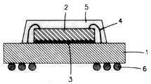
도 1은 종래 BGA 반도체 패키지의 구성을 보인 종단면도로서, 이에 도시된 바와 같이, 패턴화된 도전성 배선들(미도시)이 내설되어 있는 기판(1)이 있고, 상기 기판(1)의 상부에 반도체 칩(2)이 접착제(3)를 매개로 하여 부착되어 있으며, 상기 반도체 칩(2)과 (상기 기판(1)에 내설된) 각 배선의 일단이 다수의 도전성 와이어(4)에 의해 전기적으로 연결되어 있다. 또한, 상기 기판(1)의 상부에 상기 반도체 칩(2)과 와이어(4)들을 밀봉하고 있는 몰딩부(5)가 형성되어 있고, 상기 기판(1)의 하면에는 그 기판(1)에 내설된 각 배선의 타단에 연결되도록 다수개의 솔더볼(6)이 부착되어 있다. (여기서, 상기 배선들은 기판의 상,하부를 전기적으로 연결하여 주는 전기적 경로가 된다.)FIG. 1 is a longitudinal cross-sectional view showing a configuration of a conventional BGA semiconductor package. As shown therein, a
그러나, 도 1에 도시된 종래의 BGA 패키지는 그의 하면으로만 전기적 신호의 입출력단자가 되는 솔더볼들이 형성되어 있기 때문에, 다층의 패키지 모듈을 만들지 못하는 단점이 있다. 따라서, 제한된 면적내에서 반도체 패키지들의 적층에 의한 기능적 용량의 확대가 어려운 단점이 있다.However, the conventional BGA package shown in FIG. 1 has a disadvantage in that it is not possible to make a multi-layer package module because solder balls, which are input / output terminals of electrical signals, are formed only on the bottom surface thereof. Therefore, it is difficult to expand the functional capacity by stacking semiconductor packages within a limited area.
본 발명은 상기와 같은 종래의 BGA 반도체 패키지의 단점을 해결하기 위하여 안출한 것으로, 그 목적은 적층가능한 BGA 반도체 패키지 및 그의 제조 방법을 제공하고자 하는 것이다.The present invention has been made to solve the disadvantages of the conventional BGA semiconductor package as described above, the object is to provide a stackable BGA semiconductor package and its manufacturing method.
도 1은 종래 BGA 반도체 패키지의 종단면도.1 is a longitudinal sectional view of a conventional BGA semiconductor package.
도 2는 본 발명에 따른 BGA 반도체 패키지의 종단면도.2 is a longitudinal sectional view of a BGA semiconductor package according to the present invention;
도 3은 도 2의 배선패턴층을 기판 몸체로부터 분리하여 펼친 상태의 평면도.3 is a plan view of the wiring pattern layer of FIG.
도 4(a) - 도 4(d)는 본 발명에 따른 BGA반도체 패키지의 제조 방법을 설명하기 위한 순차적인 종단면도.Figure 4 (a)-Figure 4 (d) is a longitudinal longitudinal cross-sectional view for explaining the manufacturing method of the BGA semiconductor package according to the present invention.
도 5는 본 발명에 따른 BGA반도체 패키지 모듈의 종단면도.5 is a longitudinal cross-sectional view of a BGA semiconductor package module according to the present invention.
(도면의 주요부분에 대한 부호의 설명)(Explanation of symbols for the main parts of the drawing)
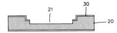
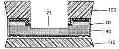
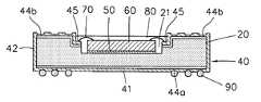
20 : 기판 몸체 21 캐비티(Cavity)20:
30 : 제 1 접착부재 40 : 배선패턴층30: first adhesive member 40: wiring pattern layer
41 : 제 1 배선패턴부42 : 제 2 배선패턴부41: first wiring pattern portion 42: second wiring pattern portion
43 : 제 3 배선패턴층 44a : 제 1 외부단자패드43: third
44b : 제 2 외부단자패드 45 : 내부단자패드44b: second external terminal pad 45: internal terminal pad
46 : 전도성 배선 50 : 제 2 접착부재46: conductive wiring 50: second adhesive member
60 : 반도체 칩 70 : 와이어60: semiconductor chip 70: wire
80 : 몰딩부 90 : 솔더볼80: molding 90: solder ball
상기와 같은 목적을 달성하기 위하여 본 발명에 따른 적층형 BGA 반도체 패키지는, 중앙부에 캐비티(cavity)(21)를 형성하고 있는 기판 몸체(20)와; 상기 기판 몸체(20)의 밑면, 측면 및 상면에 차례대로 부착되는 제 1 배선패턴부(41), 제 2 배선패턴부(42) 및 제 3 배선패턴부(43)로 이루어지고, 상기 제 1 배선패턴부(41)상에는 제 1 외부단자패드(44a)들이 형성되어 상기 솔더볼(90)들이 부착되고, 상기 제 3 배선패턴부(43)에는 상기 제 1 외부단자패드(44a)들에 대응하도록 제 2 외부단자패드(44b)들이 형성되어 있으며, 그 제 3 배선패턴부(43)의 단부에는 내부단자패드(45)들이 형성되어 상기와이어(70)의 일단과 연결되어 있고, 그리고 상기 제 1 외부단자패드(44a)들과 제 2 외부단자패드(44b)들 및 내부단자패드(45)들은 상기 배선(46)들에 의해 상호 전기적으로 연결된 배선패턴층(40)과; 상기 캐비티(21)의 저면에 부착되어 있는 반도체 칩(60)과; 상기 반도체 칩(60)과 상기 배선(46)들 사이를 전기적으로 연결하고 있는 복수개의 도전성 와이어(70)들과; 상기 반도체 칩(60)과 와이어(70)들을 밀봉하도록 상기 캐비티(21)에 채워져 있는 몰딩부(80)와; 그리고 상기 기판 몸체(20)의 하면에 형성된 상기 배선패턴층(40)의 각 배선(46)상에 대응하도록 부착되어 있는 복수개의 솔더볼(90)들을 포함하여 구성된다.In order to achieve the above object, the stacked BGA semiconductor package according to the present invention includes a
이와 같은 본 발명의 BGA 반도체 패키지에 의하면, 상기 배선패턴층의 배선들에 의해 기판의 상면과 하면에 서로 대응하는 전기적인 공통단자가 형성되기 때문에 적층된 BGA 반도체 패키지 모듈을 제작할 수 있는 이점이 있다.According to the BGA semiconductor package of the present invention, since the electrical common terminals corresponding to each other are formed on the upper and lower surfaces of the substrate by the wirings of the wiring pattern layer, there is an advantage of manufacturing a stacked BGA semiconductor package module. .
또한, 상기 제 1 외부단자패드들과 제 2 외부단자패드들 및 내부단자패드들은 상기 배선들에 의해 상호 전기적으로 연결되어 있다. 상기 제 1 및 제 2 외부단자패드들 및 내부단자패드들은 반구형의 리세스(recess)로 형성되어 있다.In addition, the first external terminal pads, the second external terminal pads and the internal terminal pads are electrically connected to each other by the wirings. The first and second external terminal pads and the internal terminal pads are formed in a hemispherical recess.
이와 같은 구성에 의하면, 상기 기판몸체의 하면과 상면에 각각 상호 대응하도록 형성된 제 1 외부단자패드들과 제 2 외부단자패드들이 전기적으로 연결되어 공통단자를 형성하기 때문에, 상기 반도체 기판의 상면과 하면 사이에 전기적인 통로가 형성된다. 또한, 상기 반구형의 제 1 외부단자내에 솔더볼이 부착되기 때문에, BGA 반도체 패키지의 제작시 솔더볼의 접착을 용이하게 하고, 완성된 BGA 반도체 패키지들의 적층시 솔더볼이 제 2 외부단자내에 안착되어 부착되므로 적층을 보다 쉽게 하는 잇점이 있다.According to this configuration, since the first external terminal pads and the second external terminal pads formed to correspond to each other on the lower surface and the upper surface of the substrate body are electrically connected to each other to form a common terminal, the upper and lower surfaces of the semiconductor substrate. An electrical passage is formed between them. In addition, since the solder balls are attached to the first external terminal of the hemispherical shape, the solder balls are easily adhered when the BGA semiconductor package is manufactured, and the solder balls are seated and attached to the second external terminal when the completed BGA semiconductor packages are stacked. There is an advantage to making it easier.
상기와 같은 목적을 달성하기 위하여 본 발명에 따른 BGA 반도체 패키지의 제조 방법은, 상.하면을 가진 기판 몸체를 제공하는 공정과; 상기 기판 몸체의 상면 중앙부에 캐비티(cavity)를 형성하는 공정과; 상기 기판 몸체의 밑면, 측면 및 상면에 차례대로 부착되는 제 1 배선패턴부, 제 2 배선패턴부 및 제 3 배선패턴부로 이루어지고, 상기 제 1 배선패턴부상에 상기 솔더볼들을 부착하기 위한 제 1 외부단자패드들이 형성되고, 상기 제 3 배선패턴부상에 상기 제 1 외부단자패드들에 대응하도록 제 2 외부단자패드들이 형성되고, 상기 제 3 배선패턴부의 단부에 상기 와이어들에 의해 상기반도체 칩과 전기적으로 연결되는 내부단자패드들이 형성되며, 상기 제 1 외부단자패드들과 제 2 외부단자패드들 및 내부단자패드들은 상기 배선들에 의해 전기적으로 연결되는 배선패턴층을 상기 기판 몸체의 상면에서 하면까지 감싸도록 부착하는 배선패턴층 형성공정과; 상기 캐비티의 저면에 반도체 칩을 부착하는 칩 부착 공정과; 복수개의 도전성 와이어들을 이용하여 상기 반도체 칩과 상기 배선들 사이를 서로 대응하도록 전기적으로 연결하는 와이어 본딩 공정과; 상기 반도체 칩과 와이어들을 밀봉하여 몰딩부를 형성하는 몰딩공정과; 그리고 상기 기판 몸체의 하면에 형성된 상기 배선들상에 솔더볼들을 부착하는 솔더볼 형성공정을 포함하여 구성된다.In order to achieve the above object, the manufacturing method of the BGA semiconductor package according to the present invention comprises the steps of providing a substrate body having a top and bottom; Forming a cavity in the center of the upper surface of the substrate body; A first wiring pattern portion, a second wiring pattern portion, and a third wiring pattern portion, which are sequentially attached to the bottom, side, and top surfaces of the substrate body; and a first external portion for attaching the solder balls onto the first wiring pattern portion. Terminal pads are formed, and second external terminal pads are formed on the third wiring pattern part to correspond to the first external terminal pads, and at the end of the third wiring pattern part, the wires are electrically connected to the semiconductor chip. Internal terminal pads are formed to be connected to each other, and the first external terminal pads, the second external terminal pads, and the internal terminal pads have a wiring pattern layer electrically connected by the wires from the upper surface to the lower surface of the substrate body. A wiring pattern layer forming step of attaching to wrap; A chip attaching step of attaching a semiconductor chip to a bottom surface of the cavity; A wire bonding process of electrically connecting the semiconductor chip and the wirings to correspond to each other using a plurality of conductive wires; A molding process of sealing the semiconductor chip and wires to form a molding part; And a solder ball forming process of attaching solder balls onto the wires formed on the bottom surface of the substrate body.
이하, 첨부 도면을 참조하여 본 발명의 바람직한 실시예에 따른 BGA 반도체 패키지 및 그의 제조 방법에 대하여 상세히 설명하기로 한다.Hereinafter, a BGA semiconductor package and a manufacturing method thereof according to a preferred embodiment of the present invention will be described in detail with reference to the accompanying drawings.
도 2는 본 발명에 따른 BGA 반도체 패키지의 종단면도로서, 절연성 물질로된 (장방형의) 기판 몸체(20)가 있고, 상기 기판 몸체(20)의 중앙부에는 캐비티(21)가 형성되어 있다. 상기 캐비티(21)를 제외한 기판 몸체(20)의 상면부터 하면에는 아교(Glue)와 같은 제 1접착부제(30)를 매개로 하여 배선패턴층(40)이 부착되어 있다. 여기서 도 3을 참조하여 상기 배선패턴층(40)의 구조를 상세히 설명하면 다음과 같다.2 is a longitudinal cross-sectional view of a BGA semiconductor package according to the present invention, in which a (rectangle)
도 3은 상기 배선패턴층(40)을 상기 기판 몸체(20)로부터 분리하여 펼친 상태의 평면도로서, 그 배선패턴층(40)은 상기 기판 몸체(20)의 밑면과 측면 및 상면에 차례대로 부착되는 제 1 배선패턴부(41)와 제 2 배선패턴부(42) 및 제 3 배선패턴부(43)로 이루어져 있다. 상기 배선패턴층(40)의 제 1 배선패턴부(41)에는 제 1 외부단자패드(44a)들이 형성되어 있고, 제 2 배선패턴부(42)에는 상기 제 1 외부단자패드(44a)와 대응하는 제 2 외부단자패드(44b)들이 형성되어 있다. 즉, 상기 제 1 외부단자패드(44a)들과 제 2 외부단자패드(44b)들은 상기 기판 몸체(20)의 상.하부에 서로 대칭되도록 형성되어 있다. 상기 배선패턴층(40)의 제 3 배선패턴부(43)의 단부에는 복수개의 내부단자패드(45)들이 상기 제 1 외부단자패드(44a)들(또는 제 2 외부단자패드(44b)들)에 대응하게 형성되어 있다. 그리고, 상기 내부단자패드(45)들과 제 1 및 제 2 외부단자패드(44a)(44b)들을 상호 전기적으로 연결하도록 패터닝된 도전성 배선(46)들이 형성되어 있다. 또한, 상기 제 1 및 제 2 외부단자패드(44a)(44b)들은 반구형의 리세스(recess)로 형성되어 있다.3 is a plan view of the
다시 도 2를 보면, 상기 캐비티(21)의 저면에 에폭시와 같은 제 2 접착부재(50)를 매개로 하여 반도체 칩(60)이 부착되어 있고, 상기 반도체 칩(60)과 상기 배선패턴층(40)에 형성된 내부단자패드(45)들 사이는 도전성 와이어(70)들을 매개로 하여 상호 전기적으로 연결되어 있다. 그리고, 상기 캐비티(21)내에는 에폭시 몰딩화합물이 채워져 상기 반도체 칩(60)과 상기 와이어(70)들을 밀봉하고 있는 몰딩부(80)가 형성되어 있으며, 상기 배선패턴층(40)의 제 1 배선패턴부(41)에 형성된 제 1 외부단자패드(44a)들상에는 솔더볼(90)들이 부착되어 있다.Referring to FIG. 2 again, the
도 4를 참조하여 본 발명에 따른 BGA반도체 패키지의 제조 방법을 설명하면 다음과 같다.Referring to Figure 4 describes the manufacturing method of the BGA semiconductor package according to the present invention.
먼저 도 4(a)와 같이, 상.하면을 가진 절연성 기판 몸체(20)를 준비하고, 상기 기판 몸체(20)의 상면 중앙부에 캐비티(21)를 형성한 후, 상기 기판 몸체(20)의 상면 및 하면에 제 1 접착부재(30)를 바른다. 상기 제 1접착부재(30)로는 아교를 사용하도록 한다.First, as shown in FIG. 4A, an
도 4(b)에 도시된 바와 같이, 상기 기판 몸체(20)의 하면과 측면 및 상면을 감싸도록 도 3에 도시된 배선패턴층(40)을 부착한 후, 상부 및 하부 몰드(100)(110)를 이용하여 열압착시켜서 상기 배선패턴층(40)이 상기 기판 몸체(20)에 견고하게 부착되도록 한다. 이때, 적어도 상기 캐비티(21)의 저면은 그 배선 패턴층(40)으로부터 외부로 노출되도록 한다.As shown in FIG. 4 (b), after attaching the
도 4(c)에 도시된 바와 같이, 상기 캐비티(21)의 저면에 제 2 접착부재(50)를 매개로 하여 반도체 칩(60)을 부착한 후, 상기 반도체 칩(60)과 상기 배선패턴층(40)의 내부단자패드(45)들 사이를 복수개의 와이어(70)들을 이용하여 상호 전기적으로 연결한다.As shown in FIG. 4C, after attaching the
도 4(d)에 도시된 바와 같이, 상기 캐비티(21) 내에 에폭시 몰딩화합물을 채워서 상기 반도체 칩(60)과 와이어(70)들을 밀봉하는 몰딩부(80)를 형성하고, 마지막으로, 상기 배선패턴층(40)의 제 1 배선패턴부(41)에 형성된 제 1 외부단자패드(44a)들 상에 솔더볼(90)들을 부착하여 본 발명의 BGA 반도체 패키지의 제조 공정을 마치도록 한다. 도 4d의 패키지는 도 2의 패키지와 동일한 패키지이다.As shown in FIG. 4 (d), an epoxy molding compound is filled in the
도 5는 도 4d의 패키지들을 적층하여 만든 BGA반도체 패키지 모듈을 도시한 것으로, 하층 BGA 반도체 패키지(200)의 제 2 외부단자패드(44b)들에 상층 BGA 반도체 패키지(300)의 솔더볼(90)들이 위치하도록 정렬하여 적층한 후, 리플로우(Reflow)공정을 실시하여 상기 솔더볼(90)들을 용융하고 굳힘으로써 상측 BGA 반도체 패키지(300)의 솔더봉(90)이 하측 BGA 반도체 패키지(200)의 제 2 외부단자패드(44b)에 전기적으로 연결된 상태로 적층 완료된다.5 illustrates a BGA semiconductor package module formed by stacking the packages of FIG. 4D, wherein the
이상 상세히 설명한 바와 같이 본 발명에 따른 적층형 BGA 반도체 패키지 및 그의 제조 방법에 의하면, 단품 BGA 반도체 패키지를 생산한 후 별도의 추기 공정 없이 리플로우 공정만으로 다층으로 된 BGA 반도체 패키지 모듈을 제작할 수 있기 때문에, 제한된 면적내에서 반도체 패키지의 기능적 용량을 확대할 수 있다.As described in detail above, according to the stacked-type BGA semiconductor package and the manufacturing method thereof according to the present invention, since the BGA semiconductor package module having a multilayer can be manufactured only by a reflow process after producing a single BGA semiconductor package, The functional capacity of a semiconductor package can be expanded within a limited area.
Claims (5)
Translated fromKoreanPriority Applications (3)
| Application Number | Priority Date | Filing Date | Title |
|---|---|---|---|
| KR1019970060262AKR100266637B1 (en) | 1997-11-15 | 1997-11-15 | Stackable ball grid array semiconductor package and a method thereof |
| JP10306451AJPH11220088A (en) | 1997-11-15 | 1998-10-28 | Laminated-type ball grid array semiconductor package and manufacture thereof |
| US09/182,195US6172423B1 (en) | 1997-11-15 | 1998-10-30 | Layer-type ball grid array semiconductor package and fabrication method thereof |
Applications Claiming Priority (1)
| Application Number | Priority Date | Filing Date | Title |
|---|---|---|---|
| KR1019970060262AKR100266637B1 (en) | 1997-11-15 | 1997-11-15 | Stackable ball grid array semiconductor package and a method thereof |
Publications (2)
| Publication Number | Publication Date |
|---|---|
| KR19990039991A KR19990039991A (en) | 1999-06-05 |
| KR100266637B1true KR100266637B1 (en) | 2000-09-15 |
Family
ID=19524819
Family Applications (1)
| Application Number | Title | Priority Date | Filing Date |
|---|---|---|---|
| KR1019970060262AExpired - Fee RelatedKR100266637B1 (en) | 1997-11-15 | 1997-11-15 | Stackable ball grid array semiconductor package and a method thereof |
Country Status (3)
| Country | Link |
|---|---|
| US (1) | US6172423B1 (en) |
| JP (1) | JPH11220088A (en) |
| KR (1) | KR100266637B1 (en) |
Families Citing this family (39)
| Publication number | Priority date | Publication date | Assignee | Title |
|---|---|---|---|---|
| KR100266693B1 (en)* | 1998-05-30 | 2000-09-15 | 김영환 | Stackable ball grid array semiconductor package and fabrication method thereof |
| US6297548B1 (en)* | 1998-06-30 | 2001-10-02 | Micron Technology, Inc. | Stackable ceramic FBGA for high thermal applications |
| KR100302593B1 (en)* | 1998-10-24 | 2001-09-22 | 김영환 | Semiconductor package and fabricating method thereof |
| JP4464527B2 (en)* | 1999-12-24 | 2010-05-19 | 大日本印刷株式会社 | Semiconductor mounting member and manufacturing method thereof |
| KR20010068781A (en)* | 2000-01-10 | 2001-07-23 | 윤종용 | Semiconductor chip package |
| US6838758B1 (en)* | 2000-05-10 | 2005-01-04 | Advanced Micro Devices, Inc. | Package and method for making an underfilled integrated circuit |
| JP3399453B2 (en)* | 2000-10-26 | 2003-04-21 | 松下電器産業株式会社 | Semiconductor device and manufacturing method thereof |
| US6358773B1 (en)* | 2000-12-27 | 2002-03-19 | Vincent Lin | Method of making substrate for use in forming image sensor package |
| US6528869B1 (en)* | 2001-04-06 | 2003-03-04 | Amkor Technology, Inc. | Semiconductor package with molded substrate and recessed input/output terminals |
| KR100443516B1 (en)* | 2001-12-24 | 2004-08-09 | 주식회사 하이닉스반도체 | Stack package and manufacturing method thereof |
| WO2003073505A1 (en)* | 2002-02-26 | 2003-09-04 | Gautham Viswanadam | Integrated circuit device and method of manufacturing thereof |
| US6806559B2 (en)* | 2002-04-22 | 2004-10-19 | Irvine Sensors Corporation | Method and apparatus for connecting vertically stacked integrated circuit chips |
| US7777321B2 (en)* | 2002-04-22 | 2010-08-17 | Gann Keith D | Stacked microelectronic layer and module with three-axis channel T-connects |
| SG127684A1 (en)* | 2002-08-19 | 2006-12-29 | Micron Technology Inc | Packaged microelectronic component assemblies |
| JP4072505B2 (en) | 2003-02-28 | 2008-04-09 | エルピーダメモリ株式会社 | Stacked semiconductor package |
| KR100521279B1 (en)* | 2003-06-11 | 2005-10-14 | 삼성전자주식회사 | Stack Chip Package |
| DE502004008576D1 (en)* | 2003-07-02 | 2009-01-15 | Siemens Home & Office Comm | SHIELDING FOR EMI-INTEGRATED ELECTRONIC COMPONENTS AND / OR CIRCUITS OF ELECTRONIC EQUIPMENT |
| DE10345391B3 (en)* | 2003-09-30 | 2005-02-17 | Infineon Technologies Ag | Multi-chip module for a semiconductor device comprises a rewiring arrangement formed as a contact device on the substrate and on a contact protrusion |
| JP2006100385A (en)* | 2004-09-28 | 2006-04-13 | Rohm Co Ltd | Semiconductor device |
| US11842972B2 (en) | 2004-09-28 | 2023-12-12 | Rohm Co., Ltd. | Semiconductor device with a semiconductor chip connected in a flip chip manner |
| JP4199724B2 (en) | 2004-12-03 | 2008-12-17 | エルピーダメモリ株式会社 | Stacked semiconductor package |
| KR100618892B1 (en)* | 2005-04-13 | 2006-09-01 | 삼성전자주식회사 | Semiconductor package achieves fan-out structure through wire bonding |
| US20060261498A1 (en)* | 2005-05-17 | 2006-11-23 | Micron Technology, Inc. | Methods and apparatuses for encapsulating microelectronic devices |
| US8389867B2 (en)* | 2005-09-30 | 2013-03-05 | Ibiden Co., Ltd. | Multilayered circuit substrate with semiconductor device incorporated therein |
| CN101361221A (en)* | 2006-04-28 | 2009-02-04 | 株式会社东芝 | Semiconductor Devices for High Frequency |
| US7833456B2 (en)* | 2007-02-23 | 2010-11-16 | Micron Technology, Inc. | Systems and methods for compressing an encapsulant adjacent a semiconductor workpiece |
| SG142321A1 (en) | 2008-04-24 | 2009-11-26 | Micron Technology Inc | Pre-encapsulated cavity interposer |
| US7863096B2 (en) | 2008-07-17 | 2011-01-04 | Fairchild Semiconductor Corporation | Embedded die package and process flow using a pre-molded carrier |
| TWI437674B (en)* | 2008-11-17 | 2014-05-11 | Advanpack Solutions Pte Ltd | Semiconductor substrate, package and device |
| US20110140265A1 (en)* | 2009-12-10 | 2011-06-16 | George Dennis Scheber | Packaging of Silicon Wafers and Mating Pieces |
| US8847376B2 (en)* | 2010-07-23 | 2014-09-30 | Tessera, Inc. | Microelectronic elements with post-assembly planarization |
| US8409923B2 (en)* | 2011-06-15 | 2013-04-02 | Stats Chippac Ltd. | Integrated circuit packaging system with underfill and method of manufacture thereof |
| JP6171402B2 (en)* | 2013-03-01 | 2017-08-02 | セイコーエプソン株式会社 | Modules, electronic devices, and mobile objects |
| CN103311214A (en)* | 2013-05-14 | 2013-09-18 | 中国科学院微电子研究所 | Substrate for laminated packaging |
| JP5554868B1 (en) | 2013-07-03 | 2014-07-23 | 太陽誘電株式会社 | Manufacturing method of substrate with cavity |
| US10468363B2 (en) | 2015-08-10 | 2019-11-05 | X-Celeprint Limited | Chiplets with connection posts |
| KR20170037331A (en)* | 2015-09-25 | 2017-04-04 | 삼성전기주식회사 | Printed circuit board and method for manufacturing the same |
| KR102537528B1 (en)* | 2016-10-19 | 2023-05-26 | 삼성전자 주식회사 | Method for manufacturing semiconductor package |
| CN113539989B (en)* | 2020-04-13 | 2023-07-21 | 烽火通信科技股份有限公司 | Multi-chip heat dissipation packaging structure and packaging method |
Citations (2)
| Publication number | Priority date | Publication date | Assignee | Title |
|---|---|---|---|---|
| US5783870A (en)* | 1995-03-16 | 1998-07-21 | National Semiconductor Corporation | Method for connecting packages of a stacked ball grid array structure |
| US5844168A (en)* | 1995-08-01 | 1998-12-01 | Minnesota Mining And Manufacturing Company | Multi-layer interconnect sutructure for ball grid arrays |
Family Cites Families (10)
| Publication number | Priority date | Publication date | Assignee | Title |
|---|---|---|---|---|
| AU645283B2 (en)* | 1990-01-23 | 1994-01-13 | Sumitomo Electric Industries, Ltd. | Substrate for packaging a semiconductor device |
| US5043794A (en)* | 1990-09-24 | 1991-08-27 | At&T Bell Laboratories | Integrated circuit package and compact assemblies thereof |
| US5172303A (en)* | 1990-11-23 | 1992-12-15 | Motorola, Inc. | Electronic component assembly |
| US5241133A (en) | 1990-12-21 | 1993-08-31 | Motorola, Inc. | Leadless pad array chip carrier |
| US5247423A (en)* | 1992-05-26 | 1993-09-21 | Motorola, Inc. | Stacking three dimensional leadless multi-chip module and method for making the same |
| US5375041A (en)* | 1992-12-02 | 1994-12-20 | Intel Corporation | Ra-tab array bump tab tape based I.C. package |
| US5741729A (en) | 1994-07-11 | 1998-04-21 | Sun Microsystems, Inc. | Ball grid array package for an integrated circuit |
| US5747874A (en)* | 1994-09-20 | 1998-05-05 | Fujitsu Limited | Semiconductor device, base member for semiconductor device and semiconductor device unit |
| US5838060A (en)* | 1995-12-12 | 1998-11-17 | Comer; Alan E. | Stacked assemblies of semiconductor packages containing programmable interconnect |
| JPH09232368A (en)* | 1996-02-20 | 1997-09-05 | Fujitsu Ltd | Semiconductor device |
- 1997
- 1997-11-15KRKR1019970060262Apatent/KR100266637B1/ennot_activeExpired - Fee Related
- 1998
- 1998-10-28JPJP10306451Apatent/JPH11220088A/enactivePending
- 1998-10-30USUS09/182,195patent/US6172423B1/ennot_activeExpired - Lifetime
Patent Citations (2)
| Publication number | Priority date | Publication date | Assignee | Title |
|---|---|---|---|---|
| US5783870A (en)* | 1995-03-16 | 1998-07-21 | National Semiconductor Corporation | Method for connecting packages of a stacked ball grid array structure |
| US5844168A (en)* | 1995-08-01 | 1998-12-01 | Minnesota Mining And Manufacturing Company | Multi-layer interconnect sutructure for ball grid arrays |
Also Published As
| Publication number | Publication date |
|---|---|
| JPH11220088A (en) | 1999-08-10 |
| KR19990039991A (en) | 1999-06-05 |
| US6172423B1 (en) | 2001-01-09 |
Similar Documents
| Publication | Publication Date | Title |
|---|---|---|
| KR100266637B1 (en) | Stackable ball grid array semiconductor package and a method thereof | |
| US6441498B1 (en) | Semiconductor substrate and land grid array semiconductor package using same | |
| KR100280398B1 (en) | Manufacturing method of stacked semiconductor package module | |
| KR970000214B1 (en) | Semiconductor device and method of producing the same | |
| US5615089A (en) | BGA semiconductor device including a plurality of semiconductor chips located on upper and lower surfaces of a first substrate | |
| JP4808408B2 (en) | Multi-chip package, semiconductor device used for the same, and manufacturing method thereof | |
| US6545366B2 (en) | Multiple chip package semiconductor device | |
| US5241133A (en) | Leadless pad array chip carrier | |
| US6072233A (en) | Stackable ball grid array package | |
| KR100240748B1 (en) | Semiconductor chip package having substrate and manufacturing method thereof, and stack package | |
| US6191370B1 (en) | Ball grid array semiconductor package and method of fabricating the same | |
| KR100475337B1 (en) | High Power Chip Scale Package and Manufacturing Method | |
| KR100520443B1 (en) | Chip scale package and its manufacturing method | |
| KR20020028473A (en) | Stack package | |
| KR100247641B1 (en) | Stacked ball grid array package and its manufacturing method | |
| KR100480908B1 (en) | method for manufacturing stacked chip package | |
| KR20000040734A (en) | Stacked micro bga package | |
| KR19990055508A (en) | Area array package and its manufacturing method | |
| JPH0669371A (en) | PGA package | |
| KR20010068504A (en) | Multichip module and assembly-stacked package using the same | |
| KR20040045696A (en) | method for fabricating semiconductor package | |
| KR20010066269A (en) | semiconductor package and metod for fabricating the same | |
| KR20000012444A (en) | Silicon Chip Package Structure | |
| JP3405718B2 (en) | Semiconductor device | |
| KR200187482Y1 (en) | Ball grid array semiconductor package |
Legal Events
| Date | Code | Title | Description |
|---|---|---|---|
| A201 | Request for examination | ||
| PA0109 | Patent application | St.27 status event code:A-0-1-A10-A12-nap-PA0109 | |
| PA0201 | Request for examination | St.27 status event code:A-1-2-D10-D11-exm-PA0201 | |
| R17-X000 | Change to representative recorded | St.27 status event code:A-3-3-R10-R17-oth-X000 | |
| PG1501 | Laying open of application | St.27 status event code:A-1-1-Q10-Q12-nap-PG1501 | |
| PN2301 | Change of applicant | St.27 status event code:A-3-3-R10-R13-asn-PN2301 St.27 status event code:A-3-3-R10-R11-asn-PN2301 | |
| E902 | Notification of reason for refusal | ||
| PE0902 | Notice of grounds for rejection | St.27 status event code:A-1-2-D10-D21-exm-PE0902 | |
| P11-X000 | Amendment of application requested | St.27 status event code:A-2-2-P10-P11-nap-X000 | |
| P13-X000 | Application amended | St.27 status event code:A-2-2-P10-P13-nap-X000 | |
| E701 | Decision to grant or registration of patent right | ||
| PE0701 | Decision of registration | St.27 status event code:A-1-2-D10-D22-exm-PE0701 | |
| GRNT | Written decision to grant | ||
| PR0701 | Registration of establishment | St.27 status event code:A-2-4-F10-F11-exm-PR0701 | |
| PR1002 | Payment of registration fee | St.27 status event code:A-2-2-U10-U11-oth-PR1002 Fee payment year number:1 | |
| PG1601 | Publication of registration | St.27 status event code:A-4-4-Q10-Q13-nap-PG1601 | |
| PR1001 | Payment of annual fee | St.27 status event code:A-4-4-U10-U11-oth-PR1001 Fee payment year number:4 | |
| PR1001 | Payment of annual fee | St.27 status event code:A-4-4-U10-U11-oth-PR1001 Fee payment year number:5 | |
| PR1001 | Payment of annual fee | St.27 status event code:A-4-4-U10-U11-oth-PR1001 Fee payment year number:6 | |
| PR1001 | Payment of annual fee | St.27 status event code:A-4-4-U10-U11-oth-PR1001 Fee payment year number:7 | |
| PR1001 | Payment of annual fee | St.27 status event code:A-4-4-U10-U11-oth-PR1001 Fee payment year number:8 | |
| PR1001 | Payment of annual fee | St.27 status event code:A-4-4-U10-U11-oth-PR1001 Fee payment year number:9 | |
| FPAY | Annual fee payment | Payment date:20090526 Year of fee payment:10 | |
| PR1001 | Payment of annual fee | St.27 status event code:A-4-4-U10-U11-oth-PR1001 Fee payment year number:10 | |
| LAPS | Lapse due to unpaid annual fee | ||
| PC1903 | Unpaid annual fee | St.27 status event code:A-4-4-U10-U13-oth-PC1903 Not in force date:20100628 Payment event data comment text:Termination Category : DEFAULT_OF_REGISTRATION_FEE | |
| PC1903 | Unpaid annual fee | St.27 status event code:N-4-6-H10-H13-oth-PC1903 Ip right cessation event data comment text:Termination Category : DEFAULT_OF_REGISTRATION_FEE Not in force date:20100628 |