KR100262402B1 - Tft lcd and its fabrication method - Google Patents
Tft lcd and its fabrication methodDownload PDFInfo
- Publication number
- KR100262402B1 KR100262402B1KR1019970014495AKR19970014495AKR100262402B1KR 100262402 B1KR100262402 B1KR 100262402B1KR 1019970014495 AKR1019970014495 AKR 1019970014495AKR 19970014495 AKR19970014495 AKR 19970014495AKR 100262402 B1KR100262402 B1KR 100262402B1
- Authority
- KR
- South Korea
- Prior art keywords
- thin film
- film transistor
- color filter
- filter layer
- lower substrate
- Prior art date
- Legal status (The legal status is an assumption and is not a legal conclusion. Google has not performed a legal analysis and makes no representation as to the accuracy of the status listed.)
- Expired - Lifetime
Links
- 238000000034methodMethods0.000titleclaimsabstractdescription31
- 238000004519manufacturing processMethods0.000titleclaimsabstractdescription22
- 239000000758substrateSubstances0.000claimsabstractdescription87
- 239000010409thin filmSubstances0.000claimsabstractdescription59
- 239000004973liquid crystal related substanceSubstances0.000claimsabstractdescription30
- 239000011159matrix materialSubstances0.000claimsabstractdescription17
- 239000010408filmSubstances0.000claimsdescription23
- 230000001681protective effectEffects0.000claimsdescription10
- 238000005530etchingMethods0.000claimsdescription3
- 239000003990capacitorSubstances0.000description7
- XYFCBTPGUUZFHI-UHFFFAOYSA-NPhosphineChemical compoundPXYFCBTPGUUZFHI-UHFFFAOYSA-N0.000description6
- 238000009825accumulationMethods0.000description5
- 229910021417amorphous siliconInorganic materials0.000description4
- 229910052751metalInorganic materials0.000description3
- 239000002184metalSubstances0.000description3
- 238000000059patterningMethods0.000description3
- 229910000073phosphorus hydrideInorganic materials0.000description3
- 230000015572biosynthetic processEffects0.000description2
- 239000011651chromiumSubstances0.000description2
- 239000011521glassSubstances0.000description2
- 238000009413insulationMethods0.000description2
- 238000012986modificationMethods0.000description2
- 230000004048modificationEffects0.000description2
- 239000004065semiconductorSubstances0.000description2
- 238000003860storageMethods0.000description2
- 241001239379Calophysus macropterusSpecies0.000description1
- VYZAMTAEIAYCRO-UHFFFAOYSA-NChromiumChemical compound[Cr]VYZAMTAEIAYCRO-UHFFFAOYSA-N0.000description1
- 229910016024MoTaInorganic materials0.000description1
- 230000000740bleeding effectEffects0.000description1
- 229910052804chromiumInorganic materials0.000description1
- 239000003086colorantSubstances0.000description1
- 238000000151depositionMethods0.000description1
- 239000012535impuritySubstances0.000description1
- 238000000206photolithographyMethods0.000description1
- 238000000623plasma-assisted chemical vapour depositionMethods0.000description1
- 239000011347resinSubstances0.000description1
- 229920005989resinPolymers0.000description1
Images

Classifications
- G—PHYSICS
- G02—OPTICS
- G02F—OPTICAL DEVICES OR ARRANGEMENTS FOR THE CONTROL OF LIGHT BY MODIFICATION OF THE OPTICAL PROPERTIES OF THE MEDIA OF THE ELEMENTS INVOLVED THEREIN; NON-LINEAR OPTICS; FREQUENCY-CHANGING OF LIGHT; OPTICAL LOGIC ELEMENTS; OPTICAL ANALOGUE/DIGITAL CONVERTERS
- G02F1/00—Devices or arrangements for the control of the intensity, colour, phase, polarisation or direction of light arriving from an independent light source, e.g. switching, gating or modulating; Non-linear optics
- G02F1/01—Devices or arrangements for the control of the intensity, colour, phase, polarisation or direction of light arriving from an independent light source, e.g. switching, gating or modulating; Non-linear optics for the control of the intensity, phase, polarisation or colour
- G02F1/13—Devices or arrangements for the control of the intensity, colour, phase, polarisation or direction of light arriving from an independent light source, e.g. switching, gating or modulating; Non-linear optics for the control of the intensity, phase, polarisation or colour based on liquid crystals, e.g. single liquid crystal display cells
- G02F1/133—Constructional arrangements; Operation of liquid crystal cells; Circuit arrangements
- G02F1/1333—Constructional arrangements; Manufacturing methods
- G02F1/1335—Structural association of cells with optical devices, e.g. polarisers or reflectors
- G02F1/133509—Filters, e.g. light shielding masks
- G02F1/133512—Light shielding layers, e.g. black matrix
- G—PHYSICS
- G02—OPTICS
- G02F—OPTICAL DEVICES OR ARRANGEMENTS FOR THE CONTROL OF LIGHT BY MODIFICATION OF THE OPTICAL PROPERTIES OF THE MEDIA OF THE ELEMENTS INVOLVED THEREIN; NON-LINEAR OPTICS; FREQUENCY-CHANGING OF LIGHT; OPTICAL LOGIC ELEMENTS; OPTICAL ANALOGUE/DIGITAL CONVERTERS
- G02F1/00—Devices or arrangements for the control of the intensity, colour, phase, polarisation or direction of light arriving from an independent light source, e.g. switching, gating or modulating; Non-linear optics
- G02F1/01—Devices or arrangements for the control of the intensity, colour, phase, polarisation or direction of light arriving from an independent light source, e.g. switching, gating or modulating; Non-linear optics for the control of the intensity, phase, polarisation or colour
- G02F1/13—Devices or arrangements for the control of the intensity, colour, phase, polarisation or direction of light arriving from an independent light source, e.g. switching, gating or modulating; Non-linear optics for the control of the intensity, phase, polarisation or colour based on liquid crystals, e.g. single liquid crystal display cells
- G02F1/133—Constructional arrangements; Operation of liquid crystal cells; Circuit arrangements
- G02F1/136—Liquid crystal cells structurally associated with a semi-conducting layer or substrate, e.g. cells forming part of an integrated circuit
- G—PHYSICS
- G02—OPTICS
- G02F—OPTICAL DEVICES OR ARRANGEMENTS FOR THE CONTROL OF LIGHT BY MODIFICATION OF THE OPTICAL PROPERTIES OF THE MEDIA OF THE ELEMENTS INVOLVED THEREIN; NON-LINEAR OPTICS; FREQUENCY-CHANGING OF LIGHT; OPTICAL LOGIC ELEMENTS; OPTICAL ANALOGUE/DIGITAL CONVERTERS
- G02F1/00—Devices or arrangements for the control of the intensity, colour, phase, polarisation or direction of light arriving from an independent light source, e.g. switching, gating or modulating; Non-linear optics
- G02F1/01—Devices or arrangements for the control of the intensity, colour, phase, polarisation or direction of light arriving from an independent light source, e.g. switching, gating or modulating; Non-linear optics for the control of the intensity, phase, polarisation or colour
- G02F1/13—Devices or arrangements for the control of the intensity, colour, phase, polarisation or direction of light arriving from an independent light source, e.g. switching, gating or modulating; Non-linear optics for the control of the intensity, phase, polarisation or colour based on liquid crystals, e.g. single liquid crystal display cells
- G02F1/133—Constructional arrangements; Operation of liquid crystal cells; Circuit arrangements
- G02F1/1333—Constructional arrangements; Manufacturing methods
- G02F1/1335—Structural association of cells with optical devices, e.g. polarisers or reflectors
- G—PHYSICS
- G02—OPTICS
- G02F—OPTICAL DEVICES OR ARRANGEMENTS FOR THE CONTROL OF LIGHT BY MODIFICATION OF THE OPTICAL PROPERTIES OF THE MEDIA OF THE ELEMENTS INVOLVED THEREIN; NON-LINEAR OPTICS; FREQUENCY-CHANGING OF LIGHT; OPTICAL LOGIC ELEMENTS; OPTICAL ANALOGUE/DIGITAL CONVERTERS
- G02F1/00—Devices or arrangements for the control of the intensity, colour, phase, polarisation or direction of light arriving from an independent light source, e.g. switching, gating or modulating; Non-linear optics
- G02F1/01—Devices or arrangements for the control of the intensity, colour, phase, polarisation or direction of light arriving from an independent light source, e.g. switching, gating or modulating; Non-linear optics for the control of the intensity, phase, polarisation or colour
- G02F1/13—Devices or arrangements for the control of the intensity, colour, phase, polarisation or direction of light arriving from an independent light source, e.g. switching, gating or modulating; Non-linear optics for the control of the intensity, phase, polarisation or colour based on liquid crystals, e.g. single liquid crystal display cells
- G02F1/133—Constructional arrangements; Operation of liquid crystal cells; Circuit arrangements
- G02F1/1333—Constructional arrangements; Manufacturing methods
- G02F1/1343—Electrodes
Landscapes
- Physics & Mathematics (AREA)
- Nonlinear Science (AREA)
- Mathematical Physics (AREA)
- Chemical & Material Sciences (AREA)
- Crystallography & Structural Chemistry (AREA)
- General Physics & Mathematics (AREA)
- Optics & Photonics (AREA)
- Liquid Crystal (AREA)
- Engineering & Computer Science (AREA)
- Microelectronics & Electronic Packaging (AREA)
- Thin Film Transistor (AREA)
Abstract
Translated fromKoreanDescription
Translated fromKorean본 발명은 박막 트랜지스터 액정표시소자에 관한 것으로, 보다 상세하게는, 컬러필터층을 하부기판에 형성하는 것에 기인하여 하부기판과 상부기판을 하나의 공정 라인에서 제조할 수 있도록 하는 박막 트랜지스터 액정표시소자 및 그의 제조 방법에 관한 것이다.BACKGROUND OF THE INVENTION 1. Field of the Invention The present invention relates to a thin film transistor liquid crystal display device, and more particularly, to a thin film transistor liquid crystal display device capable of manufacturing a lower substrate and an upper substrate in one process line due to forming a color filter layer on a lower substrate. It relates to a manufacturing method thereof.
박막 트랜지스터 액정표시소자(Thin Film Transistor Liquid Crystal Display; 이하, TFT-LCD)는 개별 스위칭 소자인 박막 트랜지스터가 형성된 하부기판과, 레드(red), 그린(green) 및 블루(blue)의 3가지 컬러필터층이 반복 배열되어 컬러화를 실현시키는 상부기판, 및 상기 상부기판과 하부기판 사이에 개재되는 액정층을 포함한다.Thin Film Transistor Liquid Crystal Display (hereinafter referred to as TFT-LCD) is a lower substrate on which a thin film transistor as an individual switching element is formed, and three colors of red, green, and blue. A filter layer is repeatedly arranged to include an upper substrate for realizing color, and a liquid crystal layer interposed between the upper substrate and the lower substrate.
도1은 종래 기술에 따른 TFT-LCD를 도시한 단면도이다. 도시된 바와 같이, 하부기판(1) 상에는 단위 화소들을 구동시키기 위한 역스태거 형태의 박막 트랜지스터(2)와, 액정 구동 전압을 인가하기 위한 ITO막으로 이루어진 화소전극(3), 및 액정 구동 전압을 유지시키기 위한 축적 캐패시터(4)가 형성된돠. 상부기판(5) 상에는 박막 트랜지스터(2)에 대응하는 부분에 박막 트랜지스터(2)를 보호함은 물론 색의 번짐을 방지하기 위한 블랙 메트릭스(6)가 형성되고, 화소전극(3)에 대응하는 부분에 컬러필터(7)가 형성되며, 상기 블랙 매트릭스(6)와 컬러필터(7)를 포함한 상부기판(5)의 전면에는 ITO막으로 이루어진 공통전극(8)이 형성된다.1 is a cross-sectional view showing a TFT-LCD according to the prior art. As illustrated, a
또한, 도시되지 않았지만, 상기와 같은 구조로 이루어진 하부기판과 상부기판을 후속 공정을 통해 합착되며, 합착된 하부기판과 상부기판의 사이에 액정이 주입되어 TFT-LCD가 완성된다.In addition, although not shown, the lower substrate and the upper substrate having the above structure are bonded to each other through a subsequent process, and the liquid crystal is injected between the bonded lower substrate and the upper substrate to complete the TFT-LCD.
그러나, 상기와 같은 TFT-LCD를 제조하기 위해서는, 하부기판을 제작하기 위한 공정라인과 상부기판을 제작하기 위한 공정라인이 각각 필요하고, 특히, 상기 공정라인들이 서로 공유되지 못하기 때문에, TFT-LCD를 제조하기 위해서는 막대한 설비 투자 비용이 소요되는 문제점이 있다.However, in order to manufacture the TFT-LCD as described above, a process line for manufacturing a lower substrate and a process line for manufacturing an upper substrate are required, and in particular, since the process lines are not shared with each other, TFT- In order to manufacture LCD, there is a problem of enormous facility investment cost.
또한, 백라이트된 빛이 액정을 통과한 이후에 컬러필터를 통과하여 액정표시소자의 컬러화를 실현하게 되므로, 색 순도면에서 액정표시소자의 화질이 저하되는 문제점이 있다.In addition, since the backlight is passed through the liquid crystal to pass through the color filter to realize the coloration of the liquid crystal display device, there is a problem that the quality of the liquid crystal display device is degraded in terms of color purity.
따라서, 상기와 같은 문제점을 해결하기 위하여 안출된 본 발명은, 상부기판상에 형성하던 컬러필터를 하부기판 상에 형성시킴으로써, 하부기판의 제작 공정과 상부기판의 제작 공정을 하나의 공정라인으로 단일화시킬 수 있고, 이에 따라, TFT-LCD를 제조하기 ;위한 설비 투자 비용을 절감할 수 있는 TFT-LCD 및 그의 제조방법을 제공하는데 그 목적이 있다.Therefore, the present invention devised to solve the above problems, by forming a color filter formed on the upper substrate on the lower substrate, unifying the manufacturing process of the lower substrate and the manufacturing process of the upper substrate in one process line. Accordingly, an object of the present invention is to provide a TFT-LCD and a method of manufacturing the same, which can reduce equipment investment costs for manufacturing a TFT-LCD.
또한, 상기와 같은 목적을 달성하기 위하여 안출된 본 발명은, 컬러필터를 하부기판에 형성시킨 백라이트된 빛이 액정을 통과하기 전에 상기 컬러필터를 먼저 통과하도록 함으로써, 액정표시소자의 색 순도를 향상시킬 수 있는 TFT-LCD 및 그이 제조 방법을 제공하는데, 그 다른 목적이 있다.In addition, the present invention devised to achieve the above object, the color light of the liquid crystal display device by improving the color purity of the liquid crystal display device by allowing the backlight, the light formed on the lower substrate to pass through the color filter first before passing through the liquid crystal To provide a TFT-LCD and a method of manufacturing the same, which have another object.
게다가, 상기와 같은 문제점을 해결하기 위하여 안출된 본 발명은, 컬러필터를 컬러화를 실현하기 위한 기능 이외에 박막 트랜지스터를 보호하기 위한 보호막으로서의 기능을 동시에 수행하게 함으로써, 보호막 형성공정을 생략시킬 수 있는 것에 기인하여 공정 단순화를 얻을 수 있는 TFT-LCD 및 그의 제조방법을 제공하는데, 그 또 다른 목적이 있다.In addition, the present invention devised to solve the above-described problems, the protective film forming process can be omitted by simultaneously performing a function as a protective film for protecting the thin film transistor in addition to the function to realize the color filter. It is another object of the present invention to provide a TFT-LCD and a method of manufacturing the same, which can obtain a process simplification.
제1도는 종래 기술에 따른 박막 트랜지스터 액정표시소자를 설명하기 위한 단면도.1 is a cross-sectional view for explaining a thin film transistor liquid crystal display device according to the prior art.
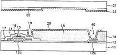
제2도는 본 발명의 실시예에 따른 박막 트랜지스터 액정표시소자를 설명하기 위한 단면도.2 is a cross-sectional view illustrating a thin film transistor liquid crystal display device according to an exemplary embodiment of the present invention.
*도면의 주요부분에 대한 부호의 설명* Explanation of symbols for main parts of the drawings
11 : 하부기판 12a : 게이트 전극11:
12b : 축적 캐피시터 하부번극 13 : 게이트 절연막12b: accumulation capacitor lower electrode 13: gate insulating film
14 : 반도체층 15 : 에치 스토퍼14
16 : 오믹 콘택층 17 : 소오스/드레인 전극16: ohmic contact layer 17: source / drain electrode
18 : 컬러필터층 19 :콘택홀18: color filter layer 19: contact hole
20 : 화소전극 21 : 상부기판20: pixel electrode 21: upper substrate
22 : 블랙 매트릭스 23 : 공통전극22
40 : 축적 캐패시터40: accumulation capacitor
상기와 같은 목적을 달성하기 위한 본 발명의 TFT-LCD는, 서로 대향하게 배치된 하부 및 상부기판; 상기 하부기판 상에 형성되며, 게이트, 소오스 및 드레인 전극을 포함하는 박막 트랜지스터; 상기 박막 트랜지스터를 포함한 상기 하부기판의 전면에 형성되며, 상기 박막 트랜지스터의 소정 부분을 노출시키는 콘택홀을 갖는 컬러필터층; 상기 콘택홀을 통하여 상기 노출된 박막 트랜지스터 부분과 콘택되도록, 상기 컬러필터층 상에 형성된 화소전극; 상기 박막 트랜지스터에 대응되는 상기 상부기판 부분 상에 형성된 블랙 메트릭스; 및 상기 블랙 매트릭스를 포함한 상기 상부기판의 전면에 형성된 공통전극을 포함하는 것을 특징으로 한다.TFT-LCD of the present invention for achieving the above object, the lower and upper substrates disposed facing each other; A thin film transistor formed on the lower substrate and including a gate, a source, and a drain electrode; A color filter layer formed on an entire surface of the lower substrate including the thin film transistor and having a contact hole exposing a predetermined portion of the thin film transistor; A pixel electrode formed on the color filter layer to be in contact with the exposed thin film transistor portion through the contact hole; A black matrix formed on the upper substrate portion corresponding to the thin film transistor; And a common electrode formed on the front surface of the upper substrate including the black matrix.
또한, 상기와 같은 목적을 달성하기 위한 본 발명의 TFT-LCD의 제조방법은, 하부기판과 상부기판을 마련하는 단계; 상기 하부기판 상에 게이트, 소오스 및 드레인 전극을 포함하는 박막 트랜지스터를 형성한믄 단계; 상기 박막 트랜지스터를 포함한 상기 하부기판의 전면에 컬러필터층을 형성하는 단계; 상기 컬러필터층을 식각하여, 상기 박막 트랜지스터의 소정 부분을 노출시키는 콘택홀을 형성하는 단계; 상기 콘택홀의 내벽 및 상기 컬러필터층 상에 화소전극을 형성하는 단계; 상기 하부기판에 형성된 박막 트랜지스터와 대응하는 상부기판 부분에 블랙 매트릭스를 형성하는 단계; 상기 블랙 매트릭스를 포함한 상부기판의 전면에 공통전극을 형성하는 단계; 상기 상부기판과 하부기판을 합착하는 단계; 및 상기 합착된 단계; 및 상기 합착된 상부기판과 하부기판 사이에 액정을 주입하는 단계를 포함하는 것을 특징으로한다.In addition, the manufacturing method of the TFT-LCD of the present invention for achieving the above object comprises the steps of providing a lower substrate and an upper substrate; Forming a thin film transistor including a gate, a source, and a drain electrode on the lower substrate; Forming a color filter layer on an entire surface of the lower substrate including the thin film transistor; Etching the color filter layer to form a contact hole exposing a portion of the thin film transistor; Forming a pixel electrode on an inner wall of the contact hole and the color filter layer; Forming a black matrix on an upper substrate portion corresponding to the thin film transistor formed on the lower substrate; Forming a common electrode on an entire surface of the upper substrate including the black matrix; Bonding the upper substrate and the lower substrate to each other; And the coalesced step; And injecting liquid crystal between the bonded upper substrate and the lower substrate.
본 발명에 따르면, 컬러필터를 하부기판 상에 형성시키는 것에 기인하여, 하부기판과 상부기판을 제작하기 위한 공정라인을 단일화시킬 수 잇으며, 이에 따라, TFT-LCD의 제조 비용을 절감시킬 수 있다. 또한 컬러필터를 하부기판 상에 형성시키기 때문에, 백라이트된 빛이 액정을 통과하기 전에 컬러필터를 통과하기 때문에, 액정표시소자의 색 순도를 향상시킬 수 있다. 게다가, 상기 컬러필터가 보호막의 기능을 동시에 수행하기 때문에, 보호막 형성 공정의 생략에 기인하여 공정 단순화를 얻을 수 있다.According to the present invention, due to the formation of the color filter on the lower substrate, it is possible to unify the process line for manufacturing the lower substrate and the upper substrate, thereby reducing the manufacturing cost of the TFT-LCD. . In addition, since the color filter is formed on the lower substrate, since the backlit light passes through the color filter before passing through the liquid crystal, color purity of the liquid crystal display device can be improved. In addition, since the color filter simultaneously performs the function of the protective film, the process simplification can be obtained due to the omission of the protective film forming process.
[실시예]EXAMPLE
이하, 첨부된 도 2를 참조하여, 본 발명의 바람직한 실시예를 보다 상세하게 설명하도록 한다.Hereinafter, with reference to the accompanying Figure 2, it will be described in detail a preferred embodiment of the present invention.
본 발명의 실시예로서, 역스태거(Inverted staggered) 형태의 박막 트랜지스터를 구비하는 TFT-LCD를 제조하기 위한 하부기판의 제조공정은, 도시된 바와 같이, 유리기판과 같은 하부기판(11)을 마련하고, 그런다음, 상기 하부기판(11)의 전면에 스퍼터를 사용하여 MoTa, MoW 또는 크론(Cr) 중 하나의 금속을 2,000 내지 3,000Å 두께로 증착한 후, 통상의 포토리소그라피 공정으로 상기 금속을 패터닝하여 게이트(12a) 및 축적 캐패시터의 하부전극(12b)을 형성한다. 이어서, 게이트(12a) 및 축적 캐패시터 하부전극(12b)을 포함한 하부기판(11)의 전면에 PECVD 방법으로 3,000Å 두께로 게이트 절연막(13)을 형성한 후, 상기 게이트 절연막(13) 상에 500Å 두께의 비도핑된 비정질실리콘층 및 2,000Å 두께의 에치 스토퍼용 절연층을 순차적으로 형성한 후, 상기 에치 스토퍼용 절연층을 패터닝하여 에치 스토퍼(15)를 형성한다.In an embodiment of the present invention, a manufacturing process of a lower substrate for manufacturing a TFT-LCD including an inverted staggered thin film transistor is provided with a
다음으로, 전체 상부에 포스핀과 같은 불순물이 도핑된 비정질실리콘을 증착하고, 그런다음, 상기 포스핀이 도핑된 비정질실리콘층과 상기 비도핑된 비정질실리콘층을 패터닝하여, 오믹 콘택층(16) 및 반도체층(15)을 형성한다. 그런다음, 도시되지는 않았지만, 외부에서 박막 트랜지스터에 신호를 넣어주기 위한 패드 부분을 오픈시키기 위하여 콘택 마스크를 이용한 식각공정을 수행한다. 그리고나서, 전체 상부에 소오스/드레인용 금속을 증착하고, 이를 패터닝하여 박막 트랜지스터의 소오스/드레인 전극(17)을 형성한다.Next, an amorphous silicon doped with an impurity such as phosphine is deposited over the entire surface, and then the amorphous silicon layer doped with the phosphine and the amorphous silicon layer doped with the phosphine are patterned to form an
계속해서, 박막 트랜지스터가 형성되 하부기판(1)의 전면에 레드(red) 의 컬러 수지를 도포하여 컬러필터층(18)을 형성하고, 상기 박막 트랜지스터의 드레인 전극 및 축적 캐패시터 하부전극(12b) 상부 영역의 절연막(13)이 노출되도록, 통상의 공정을 통해 상기 컬러필터층(18)에 콘택홀(19)을 형성한다. 여기서, 상기 컬러필터층(18)은 1 내지 3㎛ 두께의 포토-센시티브(Photo Sensitive) 한 막으로 형성되며, 특히, 상기 컬러필터층()18)은 액정표시소자의 컬러화를 실현하는 기능 이외에, 상기 박막 트랜지스터를 보호하기 위한 보호막으로서의 기능을 동시에 갖는다. 따라서, 상기 컬러필터층(18)이 보호막으로서의 기능을 갖는 것에 기인하여, 후속 공정에서 보호막 형성 공정을 생략시킬 수 있으며, 이에 따라, 공정 단순화를 얻을 수 있다. 또한, 상기 컬러필터층(18)은 레드, 그린 및 블루 중에서 하나의 색을 띄는 하나의 컬러필터층이 단위 픽셀(Pixel) 마다 각각 형성된다.Subsequently, a thin film transistor is formed to form a
다음으로, 상기 콘택홀(19)의 내벽 및 컬러필터층(18) 상에 ITO막을 증착하고, 그런다음, 상기 ITO 막을 패터닝하여, 상기 콘택홀(19)을 통하여 박막 트랜지스터의 드레인 전극과 콘택되는 화소전극(20)을 형성한다. 이때, 박막 트랜지스터에 인접된 부분에는 화소전극(20)의 형성으로 인하여 축적 캐패시터(40)가 형성된다.Next, an ITO film is deposited on the inner wall of the
그 다음, 상부기판의 제조 공정은, 유리기판과 같은 상부기판(21)을 마련한 상태에서, 상기 하부기판의 제작에 이요된 공정라인에서 하부기판(11)에 형성된 박막 트랜지스터에 대응하는 상부기판 부분에 블랙 메트릭스(22)를 형성하고, 그런다음, 상기 블랙 매트릭스(22)를 포함한 상기 상부기판(21)의 전면에 ITO 막으로 이루어진 공통전극(23)을 형성한다. 이때, 상기 블랙 매트릭스(22)는 상부기판(21)에 2,000Å 두께로 크롬을 증착한 후, 이를 패터닝하여 형성한다.Next, the manufacturing process of the upper substrate, the upper substrate portion corresponding to the thin film transistor formed on the
이후, 상기와 같은 공정을 통해 제작된 하부기판과 상부기판은 합착되고, 그런다음, 상기 하부기판과 상부기판 사이에 액정이 봉입되어 TFT-LCD가 완성된다.Thereafter, the lower substrate and the upper substrate manufactured by the above process are bonded together, and then liquid crystal is encapsulated between the lower substrate and the upper substrate to complete the TFT-LCD.
본 발명의 다른 실시예로서, 하부기판 상에 스태거, 코플래나(Coplanar) 또는 자기정렬형 등의 형태를 갖는 박막 트랜지스터를 형성한 후, 전술된 공정을 실시하여 TFT-LCD를 제조하는 것도 가능하다.In another embodiment of the present invention, after forming a thin film transistor having a shape such as a stagger, coplanar, or self-aligning type on a lower substrate, the TFT-LCD may be manufactured by performing the above-described process. It is possible.
이상에서와 같이, 본 발명은 컬러필터층을 하부기판 상에 형성하기 때문에, 하나의 공정라인으로도 TFT-LCD의 하부기판과 상부기판을 형성할 수 있으며, 이에 따라, 공정라인의 설비 투자비용을 절감할 수 있다.As described above, according to the present invention, since the color filter layer is formed on the lower substrate, the lower substrate and the upper substrate of the TFT-LCD may be formed by one process line, thereby reducing the investment cost of the process line. Can be saved.
또한, 상기 컬러필터층이 하부기판에 형성된 것에 기인하여, 백라이트된 빛이 액정층을 통과하기 전에 상기 컬러필터층을 통과하도록 할 수 있기 때문에, 액정표시소자의 색 순도를 향상시킬 수 있다.In addition, since the color filter layer is formed on the lower substrate, the backlit light may pass through the color filter layer before passing through the liquid crystal layer, thereby improving color purity of the liquid crystal display device.
게다가, 상기 컬러필터층은 박막 트랜지스터를 보호하는 보호막으로서의 기능을 하기 때문에, 후속의 보호막 형성 공정을 생략시킬 수 있으며, 이에 따라, 공정의 단순화를 얻을 수 있다.In addition, since the color filter layer functions as a protective film for protecting the thin film transistor, a subsequent protective film forming step can be omitted, thereby simplifying the process.
한편, 여기에서는 본 발명의 특정 실시예에 대하여 설명하고 도시하였지만, 당업자에 의하여 이에 대한 수정과 변형을 할 수 있다. 따라서, 이하, 특허청구의 범위는 본 발명의 진정한 사상과 범위에 속하는 한 모든 수정과 변형을 포함하는 것으로 이해할 수 있다.Meanwhile, although specific embodiments of the present invention have been described and illustrated, modifications and variations can be made by those skilled in the art. Accordingly, the following claims are to be understood as including all modifications and variations as long as they fall within the true spirit and scope of the present invention.
Claims (13)
Translated fromKoreanPriority Applications (3)
| Application Number | Priority Date | Filing Date | Title |
|---|---|---|---|
| KR1019970014495AKR100262402B1 (en) | 1997-04-18 | 1997-04-18 | Tft lcd and its fabrication method |
| US09/061,049US6191835B1 (en) | 1997-04-18 | 1998-04-16 | Thin film transistor liquid crystal display and method for manufacturing the same |
| JP10821398AJPH1124108A (en) | 1997-04-18 | 1998-04-17 | Thin film transistor type liquid crystal display element and manufacture thereof |
Applications Claiming Priority (1)
| Application Number | Priority Date | Filing Date | Title |
|---|---|---|---|
| KR1019970014495AKR100262402B1 (en) | 1997-04-18 | 1997-04-18 | Tft lcd and its fabrication method |
Publications (2)
| Publication Number | Publication Date |
|---|---|
| KR19980077392A KR19980077392A (en) | 1998-11-16 |
| KR100262402B1true KR100262402B1 (en) | 2000-08-01 |
Family
ID=19503254
Family Applications (1)
| Application Number | Title | Priority Date | Filing Date |
|---|---|---|---|
| KR1019970014495AExpired - LifetimeKR100262402B1 (en) | 1997-04-18 | 1997-04-18 | Tft lcd and its fabrication method |
Country Status (3)
| Country | Link |
|---|---|
| US (1) | US6191835B1 (en) |
| JP (1) | JPH1124108A (en) |
| KR (1) | KR100262402B1 (en) |
Families Citing this family (37)
| Publication number | Priority date | Publication date | Assignee | Title |
|---|---|---|---|---|
| KR100468594B1 (en)* | 1997-08-13 | 2005-07-11 | 삼성전자주식회사 | LCD and its manufacturing method |
| KR100508025B1 (en)* | 1997-10-27 | 2005-10-26 | 삼성전자주식회사 | Substrate for liquid crystal display device having color filter and manufacturing method thereof |
| US7821065B2 (en)* | 1999-03-02 | 2010-10-26 | Semiconductor Energy Laboratory Co., Ltd. | Semiconductor device comprising a thin film transistor comprising a semiconductor thin film and method of manufacturing the same |
| KR100284809B1 (en)* | 1999-03-18 | 2001-03-15 | 구본준 | Poly-Si Thin Film Transistor |
| KR100646781B1 (en)* | 1999-10-15 | 2006-11-17 | 삼성전자주식회사 | Thin film transistor substrate for liquid crystal display device and manufacturing method thereof |
| KR100638525B1 (en)* | 1999-11-15 | 2006-10-25 | 엘지.필립스 엘시디 주식회사 | Manufacturing Method of Array Board for Color Liquid Crystal Display |
| KR100577410B1 (en)* | 1999-11-30 | 2006-05-08 | 엘지.필립스 엘시디 주식회사 | X-ray image sensing device and its manufacturing method |
| KR100361467B1 (en)* | 2000-02-24 | 2002-11-21 | 엘지.필립스 엘시디 주식회사 | Thin Film Transistor Substrate of Liquid Crystal Display |
| JP3564417B2 (en) | 2000-05-31 | 2004-09-08 | Nec液晶テクノロジー株式会社 | Color liquid crystal display device and method of manufacturing the same |
| KR100725425B1 (en)* | 2000-07-19 | 2007-06-07 | 엘지.필립스 엘시디 주식회사 | LCD Display |
| KR100778838B1 (en)* | 2000-12-30 | 2007-11-22 | 엘지.필립스 엘시디 주식회사 | LCD and its manufacturing method |
| JP2003172946A (en) | 2001-09-28 | 2003-06-20 | Fujitsu Display Technologies Corp | Liquid crystal display device substrate and liquid crystal display device using the same |
| KR100811640B1 (en)* | 2001-10-18 | 2008-03-11 | 엘지.필립스 엘시디 주식회사 | Liquid crystal display |
| KR100855884B1 (en)* | 2001-12-24 | 2008-09-03 | 엘지디스플레이 주식회사 | Align key for liquid crystal display |
| US7102168B2 (en)* | 2001-12-24 | 2006-09-05 | Samsung Electronics Co., Ltd. | Thin film transistor array panel for display and manufacturing method thereof |
| KR100884995B1 (en)* | 2002-06-12 | 2009-02-20 | 엘지디스플레이 주식회사 | Process line of LCD and manufacturing method using same |
| KR100873497B1 (en)* | 2002-10-17 | 2008-12-15 | 삼성전자주식회사 | Integrated LCD with Fingerprint Recognition Device and Manufacturing Method Thereof |
| KR100884541B1 (en)* | 2002-12-10 | 2009-02-18 | 엘지디스플레이 주식회사 | LCD and its manufacturing method |
| KR100870701B1 (en)* | 2002-12-17 | 2008-11-27 | 엘지디스플레이 주식회사 | Array substrate for liquid crystal display device and manufacturing method |
| KR100905409B1 (en)* | 2002-12-26 | 2009-07-02 | 엘지디스플레이 주식회사 | LCD and its manufacturing method |
| KR100945579B1 (en)* | 2003-03-17 | 2010-03-08 | 삼성전자주식회사 | Display panel for display device, manufacturing method thereof and liquid crystal display device comprising the display panel |
| JP4181905B2 (en)* | 2003-03-25 | 2008-11-19 | アルプス電気株式会社 | Liquid crystal display panel and liquid crystal display device |
| JP2005258004A (en)* | 2004-03-11 | 2005-09-22 | Toshiba Matsushita Display Technology Co Ltd | Liquid crystal display element |
| FR2868629B1 (en)* | 2004-04-05 | 2006-08-25 | Atmel Corp | DIFFERENTIAL THRESHOLD VOLTAGE DETECTOR |
| KR100942265B1 (en)* | 2004-05-31 | 2010-02-16 | 엘지디스플레이 주식회사 | CIO structure liquid crystal display device and manufacturing method |
| KR101112537B1 (en)* | 2004-06-03 | 2012-02-29 | 삼성전자주식회사 | Liquid crystal display having multi domain and panel for the same |
| US7692453B2 (en)* | 2004-08-11 | 2010-04-06 | Atmel Corporation | Detector of differential threshold voltage |
| CN100376992C (en)* | 2005-03-12 | 2008-03-26 | 群康科技(深圳)有限公司 | Manufacturing method for common electrode of liquid crystal display device |
| KR20070012081A (en)* | 2005-07-22 | 2007-01-25 | 삼성전자주식회사 | Method of manufacturing thin film transistor substrate |
| US20080032431A1 (en)* | 2006-08-03 | 2008-02-07 | Tpo Displays Corp. | Method for fabricating a system for displaying images |
| TWI749283B (en) | 2008-11-28 | 2021-12-11 | 日商半導體能源研究所股份有限公司 | Liquid crystal display device |
| TWI633371B (en) | 2008-12-03 | 2018-08-21 | 半導體能源研究所股份有限公司 | Liquid crystal display device |
| KR101719350B1 (en)* | 2008-12-25 | 2017-03-23 | 가부시키가이샤 한도오따이 에네루기 켄큐쇼 | Semiconductor device and manufacturing method thereof |
| KR20120123840A (en)* | 2011-05-02 | 2012-11-12 | 삼성디스플레이 주식회사 | Liquid crystal display |
| KR102038633B1 (en)* | 2012-11-13 | 2019-10-30 | 삼성전자주식회사 | Driving device of display apparatus and Manufacturing method of the same |
| CN103219283A (en)* | 2013-03-19 | 2013-07-24 | 京东方科技集团股份有限公司 | Array substrate, manufacturing method of array substrate and display device of array substrate |
| CN103928470B (en)* | 2013-06-24 | 2017-06-13 | 上海天马微电子有限公司 | Oxide semiconductor TFT array substrate and manufacturing method thereof |
Citations (3)
| Publication number | Priority date | Publication date | Assignee | Title |
|---|---|---|---|---|
| JPS643604A (en)* | 1987-06-26 | 1989-01-09 | Hitachi Ltd | Formation of color filter |
| JPH0385529A (en)* | 1989-08-30 | 1991-04-10 | Hitachi Ltd | Thin film semiconductor display device |
| JPH0572561A (en)* | 1991-09-17 | 1993-03-26 | Sharp Corp | Active matrix substrate |
Family Cites Families (5)
| Publication number | Priority date | Publication date | Assignee | Title |
|---|---|---|---|---|
| US5499124A (en) | 1990-12-31 | 1996-03-12 | Vu; Duy-Phach | Polysilicon transistors formed on an insulation layer which is adjacent to a liquid crystal material |
| JP3240858B2 (en)* | 1994-10-19 | 2001-12-25 | ソニー株式会社 | Color display |
| KR100209277B1 (en)* | 1996-04-25 | 1999-07-15 | 구자홍 | Tft array substrate and its manufactuaring method |
| JP3264364B2 (en)* | 1997-01-21 | 2002-03-11 | シャープ株式会社 | Manufacturing method of liquid crystal display device |
| US6008872A (en)* | 1998-03-13 | 1999-12-28 | Ois Optical Imaging Systems, Inc. | High aperture liquid crystal display including thin film diodes, and method of making same |
- 1997
- 1997-04-18KRKR1019970014495Apatent/KR100262402B1/ennot_activeExpired - Lifetime
- 1998
- 1998-04-16USUS09/061,049patent/US6191835B1/ennot_activeExpired - Lifetime
- 1998-04-17JPJP10821398Apatent/JPH1124108A/enactivePending
Patent Citations (3)
| Publication number | Priority date | Publication date | Assignee | Title |
|---|---|---|---|---|
| JPS643604A (en)* | 1987-06-26 | 1989-01-09 | Hitachi Ltd | Formation of color filter |
| JPH0385529A (en)* | 1989-08-30 | 1991-04-10 | Hitachi Ltd | Thin film semiconductor display device |
| JPH0572561A (en)* | 1991-09-17 | 1993-03-26 | Sharp Corp | Active matrix substrate |
Also Published As
| Publication number | Publication date |
|---|---|
| JPH1124108A (en) | 1999-01-29 |
| US6191835B1 (en) | 2001-02-20 |
| KR19980077392A (en) | 1998-11-16 |
Similar Documents
| Publication | Publication Date | Title |
|---|---|---|
| KR100262402B1 (en) | Tft lcd and its fabrication method | |
| US5883682A (en) | Structure of a liquid crystal display and method of manufacturing the same | |
| KR100628679B1 (en) | Manufacturing method of array panel, liquid crystal display device and liquid crystal display device according to the manufacturing method | |
| US7405798B2 (en) | Liquid crystal display apparatus and method of forming the same | |
| US6038003A (en) | Liquid crystal display and method of manufacturing the same | |
| US6088072A (en) | Liquid crystal display having a bus line formed of two metal layers and method of manufacturing the same | |
| US20060290830A1 (en) | Semi-transmissive liquid crystal display device and method of manufacture thereof | |
| KR19980018480A (en) | LCD Display | |
| US5349453A (en) | Liquid crystal display device with microlenses on same plane as switching elements | |
| KR20010040214A (en) | Liquid crystal display panel and method of fabricating the same | |
| KR100626347B1 (en) | How to make TF LCD panel | |
| KR20010016714A (en) | Liquid crystal display device | |
| KR100715907B1 (en) | Liquid crystal display | |
| JP2000122096A (en) | Reflective liquid crystal display device and its manufacture | |
| KR100413512B1 (en) | an array panel for liquid crystal display and manufacturing method thereof | |
| KR100904519B1 (en) | Liquid crystal display device and manufacturing method thereof | |
| KR100648422B1 (en) | Array substrate for liquid crystal display device and manufacturing method thereof | |
| KR20020027727A (en) | liquid crystal display and manufacturing method thereof | |
| KR100603852B1 (en) | Method for manufacturing liquid crystal display device using diffraction exposure technique | |
| KR100268105B1 (en) | Thin Film Transistor Board and Manufacturing Method | |
| KR20050067624A (en) | Liquid crystal display and manufacturing method thereof | |
| KR100924750B1 (en) | LCD and its manufacturing method | |
| KR101258084B1 (en) | Liquid crystal display device and fabrication method thereof | |
| JP2002148657A (en) | Liquid crystal display | |
| KR100508025B1 (en) | Substrate for liquid crystal display device having color filter and manufacturing method thereof |
Legal Events
| Date | Code | Title | Description |
|---|---|---|---|
| A201 | Request for examination | ||
| PA0109 | Patent application | Patent event code:PA01091R01D Comment text:Patent Application Patent event date:19970418 | |
| PA0201 | Request for examination | Patent event code:PA02012R01D Patent event date:19970418 Comment text:Request for Examination of Application | |
| PG1501 | Laying open of application | ||
| E902 | Notification of reason for refusal | ||
| PE0902 | Notice of grounds for rejection | Comment text:Notification of reason for refusal Patent event date:19990917 Patent event code:PE09021S01D | |
| E701 | Decision to grant or registration of patent right | ||
| PE0701 | Decision of registration | Patent event code:PE07011S01D Comment text:Decision to Grant Registration Patent event date:20000214 | |
| GRNT | Written decision to grant | ||
| PR0701 | Registration of establishment | Comment text:Registration of Establishment Patent event date:20000501 Patent event code:PR07011E01D | |
| PR1002 | Payment of registration fee | Payment date:20000502 End annual number:3 Start annual number:1 | |
| PG1601 | Publication of registration | ||
| PR1001 | Payment of annual fee | Payment date:20030529 Start annual number:4 End annual number:4 | |
| PR1001 | Payment of annual fee | Payment date:20040406 Start annual number:5 End annual number:5 | |
| PR1001 | Payment of annual fee | Payment date:20050422 Start annual number:6 End annual number:6 | |
| PR1001 | Payment of annual fee | Payment date:20060502 Start annual number:7 End annual number:7 | |
| PR1001 | Payment of annual fee | Payment date:20070425 Start annual number:8 End annual number:8 | |
| PR1001 | Payment of annual fee | Payment date:20080408 Start annual number:9 End annual number:9 | |
| PR1001 | Payment of annual fee | Payment date:20090504 Start annual number:10 End annual number:10 | |
| PR1001 | Payment of annual fee | Payment date:20100315 Start annual number:11 End annual number:11 | |
| PR1001 | Payment of annual fee | Payment date:20110419 Start annual number:12 End annual number:12 | |
| PR1001 | Payment of annual fee | Payment date:20120406 Start annual number:13 End annual number:13 | |
| FPAY | Annual fee payment | Payment date:20130417 Year of fee payment:14 | |
| PR1001 | Payment of annual fee | Payment date:20130417 Start annual number:14 End annual number:14 | |
| FPAY | Annual fee payment | Payment date:20140421 Year of fee payment:15 | |
| PR1001 | Payment of annual fee | Payment date:20140421 Start annual number:15 End annual number:15 | |
| FPAY | Annual fee payment | ||
| PR1001 | Payment of annual fee | Payment date:20150416 Start annual number:16 End annual number:16 | |
| FPAY | Annual fee payment | Payment date:20160418 Year of fee payment:17 | |
| PR1001 | Payment of annual fee | Payment date:20160418 Start annual number:17 End annual number:17 | |
| EXPY | Expiration of term | ||
| PC1801 | Expiration of term |