KR100260996B1 - Array type semiconductor package using a lead frame and its manufacturing method - Google Patents
Array type semiconductor package using a lead frame and its manufacturing methodDownload PDFInfo
- Publication number
- KR100260996B1 KR100260996B1KR1019970054507AKR19970054507AKR100260996B1KR 100260996 B1KR100260996 B1KR 100260996B1KR 1019970054507 AKR1019970054507 AKR 1019970054507AKR 19970054507 AKR19970054507 AKR 19970054507AKR 100260996 B1KR100260996 B1KR 100260996B1
- Authority
- KR
- South Korea
- Prior art keywords
- lead frame
- semiconductor chip
- heat sink
- lead
- input
- Prior art date
- Legal status (The legal status is an assumption and is not a legal conclusion. Google has not performed a legal analysis and makes no representation as to the accuracy of the status listed.)
- Expired - Fee Related
Links
Images


Classifications
- H—ELECTRICITY
- H01—ELECTRIC ELEMENTS
- H01L—SEMICONDUCTOR DEVICES NOT COVERED BY CLASS H10
- H01L23/00—Details of semiconductor or other solid state devices
- H01L23/28—Encapsulations, e.g. encapsulating layers, coatings, e.g. for protection
- H—ELECTRICITY
- H01—ELECTRIC ELEMENTS
- H01L—SEMICONDUCTOR DEVICES NOT COVERED BY CLASS H10
- H01L2224/00—Indexing scheme for arrangements for connecting or disconnecting semiconductor or solid-state bodies and methods related thereto as covered by H01L24/00
- H01L2224/01—Means for bonding being attached to, or being formed on, the surface to be connected, e.g. chip-to-package, die-attach, "first-level" interconnects; Manufacturing methods related thereto
- H01L2224/10—Bump connectors; Manufacturing methods related thereto
- H01L2224/15—Structure, shape, material or disposition of the bump connectors after the connecting process
- H01L2224/16—Structure, shape, material or disposition of the bump connectors after the connecting process of an individual bump connector
- H01L2224/161—Disposition
- H01L2224/16151—Disposition the bump connector connecting between a semiconductor or solid-state body and an item not being a semiconductor or solid-state body, e.g. chip-to-substrate, chip-to-passive
- H01L2224/16221—Disposition the bump connector connecting between a semiconductor or solid-state body and an item not being a semiconductor or solid-state body, e.g. chip-to-substrate, chip-to-passive the body and the item being stacked
- H01L2224/16245—Disposition the bump connector connecting between a semiconductor or solid-state body and an item not being a semiconductor or solid-state body, e.g. chip-to-substrate, chip-to-passive the body and the item being stacked the item being metallic
- H—ELECTRICITY
- H01—ELECTRIC ELEMENTS
- H01L—SEMICONDUCTOR DEVICES NOT COVERED BY CLASS H10
- H01L2224/00—Indexing scheme for arrangements for connecting or disconnecting semiconductor or solid-state bodies and methods related thereto as covered by H01L24/00
- H01L2224/01—Means for bonding being attached to, or being formed on, the surface to be connected, e.g. chip-to-package, die-attach, "first-level" interconnects; Manufacturing methods related thereto
- H01L2224/42—Wire connectors; Manufacturing methods related thereto
- H01L2224/47—Structure, shape, material or disposition of the wire connectors after the connecting process
- H01L2224/48—Structure, shape, material or disposition of the wire connectors after the connecting process of an individual wire connector
- H01L2224/4805—Shape
- H01L2224/4809—Loop shape
- H01L2224/48091—Arched
- H—ELECTRICITY
- H01—ELECTRIC ELEMENTS
- H01L—SEMICONDUCTOR DEVICES NOT COVERED BY CLASS H10
- H01L2224/00—Indexing scheme for arrangements for connecting or disconnecting semiconductor or solid-state bodies and methods related thereto as covered by H01L24/00
- H01L2224/73—Means for bonding being of different types provided for in two or more of groups H01L2224/10, H01L2224/18, H01L2224/26, H01L2224/34, H01L2224/42, H01L2224/50, H01L2224/63, H01L2224/71
- H01L2224/732—Location after the connecting process
- H01L2224/73251—Location after the connecting process on different surfaces
- H01L2224/73253—Bump and layer connectors
- H—ELECTRICITY
- H01—ELECTRIC ELEMENTS
- H01L—SEMICONDUCTOR DEVICES NOT COVERED BY CLASS H10
- H01L2224/00—Indexing scheme for arrangements for connecting or disconnecting semiconductor or solid-state bodies and methods related thereto as covered by H01L24/00
- H01L2224/73—Means for bonding being of different types provided for in two or more of groups H01L2224/10, H01L2224/18, H01L2224/26, H01L2224/34, H01L2224/42, H01L2224/50, H01L2224/63, H01L2224/71
- H01L2224/732—Location after the connecting process
- H01L2224/73251—Location after the connecting process on different surfaces
- H01L2224/73265—Layer and wire connectors
- H—ELECTRICITY
- H01—ELECTRIC ELEMENTS
- H01L—SEMICONDUCTOR DEVICES NOT COVERED BY CLASS H10
- H01L2924/00—Indexing scheme for arrangements or methods for connecting or disconnecting semiconductor or solid-state bodies as covered by H01L24/00
- H01L2924/15—Details of package parts other than the semiconductor or other solid state devices to be connected
- H01L2924/161—Cap
- H01L2924/1615—Shape
- H01L2924/16152—Cap comprising a cavity for hosting the device, e.g. U-shaped cap
Landscapes
- Physics & Mathematics (AREA)
- Condensed Matter Physics & Semiconductors (AREA)
- General Physics & Mathematics (AREA)
- Engineering & Computer Science (AREA)
- Computer Hardware Design (AREA)
- Microelectronics & Electronic Packaging (AREA)
- Power Engineering (AREA)
- Lead Frames For Integrated Circuits (AREA)
Abstract
Translated fromKoreanDescription
Translated fromKorean본 발명은 리드프레임을 이용한 어레이형 반도체패키지 및 그 제조 방법에 관한 것으로, 보다 상세하게 설명하면 탭(Tape Automated Bonding)본딩의 하나인 갱본딩(Gang Bonding) 방법을 이용하여 봉지수단의 두께를 최소화함으로써 박형화한 반도체패키지를 구비하고, 또한 반도체패키지내의 여유공간을 최대한 활용함으로써 고집적도의 대형 반도체칩을 수용할 수 있는 리드프레임을 이용한 어레이형 반도체패키지 및 그 제조 방법에 관한 것이다.The present invention relates to an array type semiconductor package using a lead frame and a method of manufacturing the same. More specifically, the thickness of the encapsulation means is minimized by using a gang bonding method, which is one of tab automated bonding. The present invention relates to an array type semiconductor package using a lead frame capable of accommodating a thin semiconductor package and maximizing a free space in the semiconductor package to accommodate large semiconductor chips of high density.
일반적으로 반도체패키지라 함은 각종 전자 회로 및 배선이 적층되어 형성된 단일 소자 및 집적 회로 등의 반도체칩을 먼지, 습기, 전기적, 기계적 부하 등의 각종 외부 환경으로부터 보호하고 상기 반도체칩의 전기적 성능을 최적화, 극대화시키기 위해 리드프레임(Lead Frame)이나 인쇄회로기판(Printed Circuit Board) 등을 이용해 메인보드(Main Board)로의 신호 입/출력 단자를 형성하고 봉지수단을 이용하여 몰딩(Molding)한 것을 말한다.In general, a semiconductor package is to protect a semiconductor chip such as a single device and an integrated circuit formed by stacking various electronic circuits and wirings from various external environments such as dust, moisture, electrical and mechanical loads, and to optimize the electrical performance of the semiconductor chip. In order to maximize, it means that the signal input / output terminals to the main board are formed using a lead frame or a printed circuit board, and molded using an encapsulation means.
이러한 반도체패키지는 최근 반도체칩의 진보된 집적화 기술과 전자기기의 소형화에 따라서 이를 뒷받침하기 위해 경박단소(輕薄短少)화의 추세에 있으며 핀그리드어레이(Pin Grid Array)반도체패키지, 볼그리드어레이(Ball Grid Array)반도체패키지, 리드프레임을 이용한 어레이형 반도체패키지 등의 수요가 증가하고 있다. 이러한 반도체패키지는 섭스트레이트(Substrate)로서 인쇄회로기판을 이용한 PGA반도체패키지, BGA반도체패키지와 리드프레임을 이용한 어레이형 반도체패키지로 분류할 수 있으며 이중에서도 리드프레임을 이용한 어레이형 반도체패키지의 구조를 첨부된 도1a 및 도1b를 참조하여 설명하면 다음과 같다.These semiconductor packages are in the trend of light and thin in order to support the recent integration of semiconductor chips and miniaturization of electronic devices. Pin grid array semiconductor packages and ball grid arrays (Ball) Demand for semiconductor packages and array type semiconductor packages using lead frames is increasing. Such semiconductor packages can be classified as PGA semiconductor packages using printed circuit boards, array type semiconductor packages using BGA semiconductor packages and lead frames, and the structure of array type semiconductor packages using lead frames is attached. A description with reference to FIGS. 1A and 1B is as follows.
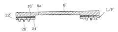
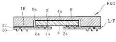
먼저 다수의 입/출력패드(2')가 형성된 반도체칩(4')이 중앙에 위치되어 있고, 상기 반도체칩(4')의 상면에는 그 반도체칩(4')의 작동시 발생하는 열을 외부로 방출하기 위해 방열판(6')이 접착제(4a')로 접착되어 있다. 상기 방열판(6')은 중앙하부면에 단면의 형태가 사각인 요부(6a')가 형성되어 있으며 그 요부(6a')에 반도체칩(4')이 안착되어 있다. 또한 상기 방열판(6')의 하부, 보다 자세하게는 반도체칩(4')이 접착된 곳 또는 방열판(6')에 형성된 요부(6a')를 제외한 방열판(6')의 저면에는 양면접착테이프(18')에 의해 리드프레임(L/F')이 접착되어 있다. 상기 리드프레임(L/F')은 중앙부에 반도체칩(4')이 위치할 수 있도록 공간부(32')가 형성되어 있고, 상기 공간부(32')의 외주변에는 다수의 리드(22')가 회로패턴을 형성하고 있는데, 이것은 공간부(32') 가까운 곳에 본드핑거(24')가 형성되어 있고, 상기 본드핑거(24')의 연장선에는 방열판(6')의 하부를 향하여 돌출부(26')가 다수 형성된 형태를 한다. 상기 리드프레임(L/F')의 본드핑거(24')는 반도체칩(4')의 입/출력패드(2')와 전도성와이어로 본딩되어 있으며 상기 돌출부(26')는 메인보드(Main Board)에의 신호 입/출력수단으로서 솔더볼(12')이 융착되어 있다. 마지막으로 상기 반도체칩(4') 등을 외부의 환경으로부터 보호하기 위해 반도체칩(4'), 전도성와이어 및 리드프레임(L/F')의 소정영역이 봉지수단(10')로 봉지되어 있다.First, a semiconductor chip 4 'having a plurality of input / output pads 2' is positioned at the center, and heat generated during operation of the semiconductor chip 4 'is disposed on an upper surface of the semiconductor chip 4'. The heat sink 6 'is bonded with an adhesive 4a' to release to the outside. The heat sink 6 'is formed with a
여기서 상기 리드프레임(L/F')의 구조를 좀더 자세히 설명하면 도1b의 평면도에 도시된 바와 같이, 중앙에 반도체칩(4')이 위치하도록 소정의 공간부(32')가 구비되어 있고, 그 공간부(32') 주변으로는 다수의 리드(22')로 복잡한 회로패턴이 형성되어 있다. 즉, 상기 리드(22')는 공간부(32')의 외주변에 반도체칩(4')의 입/출력패드(2')와 와이어본딩(Wire Bonding)되는 본드핑거(24')가 구비되어 있고, 상기 본드핑거(24')에 연장된 리드(22')에는 다수의 돌출부(26')가 할프에칭(Half Etching)기술에 의해 형성되어 있다.Herein, the structure of the lead frame L / F 'will be described in more detail. As shown in the plan view of FIG. 1B, a predetermined space portion 32' is provided so that the semiconductor chip 4 'is located at the center thereof. In the periphery of the space 32 ', a complicated circuit pattern is formed of a plurality of leads 22'. That is, the lead 22 'includes a bond finger 24' which is wire bonded with an input / output pad 2 'of the semiconductor chip 4' around the space part 32 '. In the lead 22 'extending to the bond finger 24', a plurality of protrusions 26 'are formed by a half etching technique.
도면중 미설명 부호 34'는 리드프레임(L/F')의 최외각에 형성되어 소정의 형태를 유지시키는 사이드레일이며, 부호 36'은 리드프레임(L/F')의 제조 공정중 핀에 삽입되어 이동될 수 있도록 하는 이송용통공이다.In the figure, reference numeral 34 'denotes a side rail formed at the outermost side of the lead frame L / F' to maintain a predetermined shape, and reference numeral 36 'denotes a pin in the manufacturing process of the lead frame L / F'. It is a feed hole for insertion and movement.
한편, 이러한 리드프레임(L/F')을 이용한 어레이형 반도체패키지(PKG')의 제조 방법을 첨부된 도3a 내지 도3f를 이용하여 설명하면 다음과 같다.Meanwhile, a method of manufacturing the array type semiconductor package PKG 'using the lead frame L / F' will be described with reference to FIGS. 3A through 3F.
먼저 상기한 바와 같은 리드프레임(L/F')을 소정의 위치로 이동시켜 고정시키고(도3a), 상기 리드프레임(L/F')의 상면에는 양면접착테이프(18')를 이용하여 방열판(6')을 접착시킨다.(도3b 및 도3c) 그런후에 상기 리드프레임(L/F')의 공간부(32') 즉, 방열판(6')의 중앙부 하단의 요부(6a')에 반도체칩(4')을 접착제(4a')로 접착시키고 상기 리드프레임(L/F')의 본드핑거(24')와 그 반도체칩(4')의 입/출력패드(2')를 전도성와이어로 본딩시킨다.(도3d) 이어서 상기 반도체칩(4'), 전도성와이어 및 리드프레임(L/F')의 일부를 모두 봉지수단(10')으로 봉지한다.(도3e) 또한 상기 리드프레임(L/F')의 돌출부(26') 저면에는 고온의 상태에서 솔더볼(12')을 녹여 붙인다.(도3f)First, the lead frame L / F 'as described above is moved to a predetermined position and fixed (FIG. 3A), and the heat sink is formed on the upper surface of the lead frame L / F' using a double-sided
이상에서와 같은 구조 및 제조 방법으로 이루어진 종래의 리드프레임(L/F')을 이용한 어레이형 반도체패키지(PKG')는, 와이어본딩시 형성되는 와이어꺽임높이로 인해 봉지수단(10')의 면적 및 두께가 커지게 된다. 따라서 리드(22')의 돌출부(26')를 메인보드에의 신호 입/출력 수단으로 직접 사용할 수 없으며 이로 인해 상기 리드(22')의 돌출부(26')에 솔더볼(12')을 융착시켜야만 하고 이는 반도체패키지(PKG')의 높이를 크게하는 요인이 되고 있다. 또한 솔더볼(12') 자체에 소비되는 비용으로 인해 생산 단가가 증가하는 문제점이 있다.The array-type semiconductor package PKG 'using the conventional lead frame L / F' having the structure and manufacturing method as described above has an area of the encapsulation means 10 'due to the wire bending height formed during wire bonding. And the thickness becomes large. Therefore, the protrusion 26 'of the lead 22' cannot be directly used as a signal input / output means to the main board, and therefore, the solder ball 12 'must be fused to the protrusion 26' of the lead 22 '. This is a factor that increases the height of the semiconductor package (PKG '). In addition, there is a problem that the production cost increases due to the cost consumed in the solder ball (12 ') itself.
아울러 상기 반도체칩(4')의 입/출력패드(2')와 리드(22')의 본드핑거(24') 사이에 형성되는 와이어본딩을 위해 상기 입/출력패드(2')와 본드핑거(24') 사이에는 항상 소정의 공간 또는 거리가 필요하게 됨으로서 고집적도의 대형반도체칩(4')을 수용하고자 할 경우에는 반도체패키지(PKG')의 크기도 비례하여 커지는 문제점이 있다. 이러한 문제점은 결국 메인보드에 반도체패키지(PKG')를 실장할 경우 그 실장 밀도를 저하시킴으로서 전자기기 부피의 소형화 추세에 걸림돌이 되고 있다.In addition, the input / output pad 2 'and the bond finger for wire bonding formed between the input / output pad 2' of the semiconductor chip 4 'and the bond finger 24' of the lead 22 '. Since a predetermined space or distance is always required between 24 ', when the large-sized semiconductor chip 4' is to be accommodated, the size of the semiconductor package PKG 'is also increased in proportion. This problem, after mounting a semiconductor package (PKG ') on the main board is lowering the mounting density, which is an obstacle to the trend of miniaturization of electronic device volume.
또한 제조 공정에 있어서 리드(22')의 본드핑거(24')와 반도체칩(4')의 입/출력패드(2')를 순차적으로 와이어본딩하여야 함으로써 그 시간이 오래 소비되고 또한 와이어를 사용함으로서 반도체칩(4')의 입/출력패드(2')와 리드(22')의 본드핑거(24') 사이에 전기저항이 크게 나타나 반도체칩(4')의 기능을 저하시키는 문제점이 있다.In addition, in the manufacturing process, the bond finger 24 'of the lead 22' and the input / output pad 2 'of the semiconductor chip 4' must be wire-bonded in sequence, thereby consuming a long time and using a wire. As a result, a large electric resistance is generated between the input / output pad 2 'of the semiconductor chip 4' and the bond finger 24 'of the lead 22', thereby degrading the function of the semiconductor chip 4 '. .
따라서 본 발명은 상기와 같은 종래의 문제점을 해결하기 위해 안출한 것으로 본 발명의 첫번째 목적은 와이어본딩 대신 탭본딩의 한종류인 갱본딩 방법을 이용하여 반도체패키지의 두께를 박형화하고 또한 반도체패키지내 공간의 여유도를 높여 같은 크기의 반도체패키지에 보다 더 큰 반도체칩을 수용할 수 있으며 동시다발적인 본딩으로서 짧은 시간에 본딩작업을 완료할 수 있는 리드프레임을 이용한 반도체패키지를 제공하는 데 있다.Therefore, the present invention has been made to solve the above-mentioned conventional problems. The first object of the present invention is to reduce the thickness of the semiconductor package by using a gang bonding method, which is one of tab bonding instead of wire bonding, and to reduce the space of the semiconductor package. It is to provide a semiconductor package using a lead frame that can accommodate larger semiconductor chips in a semiconductor package of the same size by increasing the margin and can simultaneously complete the bonding work in a short time as multiple bonding.
두번째 목적은 입/출력 수단으로 상기 돌출부에 솔더 도금만을 실시하여 사용할 수 있도록 함으로서 솔더볼 사용으로 인한 비용을 절감할 수 있는 리드프레임을 이용한 반도체패키지를 제공하는데 있다.A second object is to provide a semiconductor package using a lead frame that can reduce the cost due to the use of solder balls by using only the solder plating on the protrusion as an input / output means.
세번째 목적은 반도체칩의 입/출력패드와 리드프레임의 본드핑거 연결 수단을 범프로 함으로써 그 전기적 저항을 감소시켜 반도체칩의 기능을 향상시킬 수 있는 리드프레임을 이용한 반도체패키지를 제공하는데 있다.A third object of the present invention is to provide a semiconductor package using a lead frame capable of improving the function of the semiconductor chip by reducing its electrical resistance by bumping the bond finger connecting means of the input / output pad of the semiconductor chip and the lead frame.
네번째 목적은 상기와 같은 리드프레임을 이용한 반도체패키지의 제조 방법을 제공하는데 있다.A fourth object is to provide a method of manufacturing a semiconductor package using the lead frame as described above.
도1a는 종래의 리드프레임을 이용한 어레이형 반도체패키지의 구조를 나타낸 단면도이고, 도1b는 할프에칭기술로 제조된 리드프레임을 도시한 평면도이다.FIG. 1A is a cross-sectional view illustrating a structure of an array type semiconductor package using a conventional lead frame, and FIG. 1B is a plan view of a lead frame manufactured by a half etching technique.
도2a내지 도2f는 종래 리드프레임을 이용한 어레이형 반도체패키지의 제조 방법을 나타낸 상태도이다.2A to 2F are state diagrams illustrating a method of manufacturing an array type semiconductor package using a conventional lead frame.
도3은 본 발명에 의한 리드프레임을 이용한 어레이형 반도체패키지의 구조를 도시한 단면도이다.3 is a cross-sectional view showing the structure of an array type semiconductor package using a lead frame according to the present invention.
도4a 내지 도4e는 본 발명에 의한 리드프레임을 이용한 어레이형 반도체패키지의 제조 방법을 나타낸 상태도이다.4A to 4E are state diagrams illustrating a method of manufacturing an array type semiconductor package using a lead frame according to the present invention.
도5a 및 도5b는 본 발명에 의한 리드프레임을 이용한 어레이형 반도체패키지의 다른 실시예를 도시한 단면도이다.5A and 5B are sectional views showing another embodiment of the array type semiconductor package using the lead frame according to the present invention.
- 도면중 주요 부분에 대한 부호의 설명 --Explanation of symbols for the main parts of the drawings-
PKG ; 반도체패키지 L/F ; 리드프레임(Lead Frame)PKG; Semiconductor package L / F; Lead Frame
2 ; 입/출력패드(Input/Output Pad) 4 ; 반도체칩2 ; Input /
4a ; 접착제 6 ; 방열판4a;
6a ; 요부 10 ; 봉지수단6a;
12 ; 솔더볼(Solder Ball) 14 ; 범프(Bump)12;
18 ; 양면접착테이프 22 ; 리드18; Double sided
24 ; 본드핑거(Bond Finger) 26 ; 돌출부24;
26a ; 솔더26a; Solder
상기한 목적을 달성하기 위해 본 발명에 의한 리드프레임을 이용한 어레이형 반도체패키지는 저면에 다수의 입/출력패드를 갖는 반도체칩과, 상기 반도체칩의 상면에 접착제로 접착되어 반도체칩의 열을 외부로 방출하는 방열판과, 상기 방열판의 저면에 위치하며 본드핑거와 하부를 향해 돌출된 돌출부와 상기 본드핑거와 돌출부를 서로 연결하는 리드로 이루어진 리드프레임과, 상기 리드프레임의 상면과 방열판의 저면을 접착시키는 양면접착테이프와, 상기 반도체칩의 입/출력패드와 리드프레임의 본드핑거가 서로 전기적으로 도통되도록 연결하는 범프와, 상기 반도체칩, 범프 및 리드프레임의 본드핑거, 리드, 저면을 제외한 돌출부를 봉지하는 봉지수단을 포함하여 이루어진 것을 특징으로 한다.In order to achieve the above object, an array type semiconductor package using a lead frame according to the present invention is a semiconductor chip having a plurality of input / output pads on a bottom surface thereof, and is bonded to an upper surface of the semiconductor chip with an adhesive to heat heat of the semiconductor chip. Bonding a heat sink radiating to the bottom surface of the heat sink, a lead frame formed on the bottom surface of the heat sink, and a lead frame protruding toward the bottom, and a lead connecting the bond finger and the protrusion to each other, and an upper surface of the lead frame and a bottom surface of the heat sink A double-sided adhesive tape, a bump for connecting the input / output pad of the semiconductor chip and the bond finger of the lead frame to be electrically connected to each other, and a protrusion except for the bond finger, lead, and bottom of the semiconductor chip, bump and lead frame. It characterized in that it comprises a sealing means for sealing.
또한 상기한 목적을 달성하기 위해 본 발명에 의한 리드프레임을 이용한 어레이형 반도체패키지의 제조 방법은 저면 중앙부에 단면의 형태가 사각인 요부가 형성된 방열판을 구비하는 방열판 준비 단계와, 상기 방열판의 사각 요부 저면에 입/출력패드에는 범프가 융착되어 있는 반도체칩을 접착제로 접착하는 반도체칩 접착 단계와, 상기 방열판 저면의 요부 외주변에 양면접착테이프로 본드핑거, 리드 및 돌출부로 이루어진 리드프레임을 접착하는 리드프레임 접착 단계와, 상기 반도체칩의 모든 입/출력패드에 형성된 범프와 리드프레임의 모든 본드핑거를 고온의 환경하에서 동시에 융착하는 갱본딩 단계와, 상기 반도체칩, 리드프레임 등을 봉지수단으로 밀봉하는 봉지 단계를 포함하여 이루어진 것을 특징으로 한다.In addition, in order to achieve the above object, a method of manufacturing an array-type semiconductor package using a lead frame according to the present invention includes a heat sink preparing step having a heat sink formed with a recess having a rectangular cross section at the bottom center, and a rectangular recess of the heat sink. A semiconductor chip bonding step of bonding a bumped semiconductor chip with an adhesive to an input / output pad on a bottom surface, and a lead frame composed of a bond finger, a lead, and a protrusion with a double-sided adhesive tape on the outer periphery of the bottom of the heat sink. A lead frame bonding step, a gang bonding step of fusion bonding all the bumps formed on all the input and output pads of the semiconductor chip and all the bond fingers of the lead frame in a high temperature environment at the same time, sealing the semiconductor chip, the lead frame, etc. with sealing means Characterized in that it comprises a sealing step.
이하 본 발명이 속하는 기술 분야에서 통상의 지식을 가진 자가 본 발명을 용이하게 실시할 수 있을 정도로 본 발명의 바람직한 실시예를 첨부된 도면을 참조하여 상세하게 설명하면 다음과 같다.Hereinafter, exemplary embodiments of the present invention will be described in detail with reference to the accompanying drawings so that those skilled in the art may easily implement the present invention.
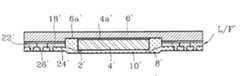
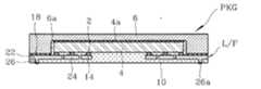
먼저 도3을 이용하여 본 발명에 의한 리드프레임(L/F)을 이용한 어레이형 반도체패키지(PKG)의 구조를 설명하면 다음과 같다.First, the structure of the array type semiconductor package PKG using the lead frame L / F according to the present invention will be described with reference to FIG. 3.
중앙부에는 저면에 다수의 입/출력패드(2)가 형성된 반도체칩(4)이 위치되어 있고, 상기 반도체칩(4)의 상면에는 접착제(4a)로 방열판(6)이 접착되어 반도체칩(4)의 작동시 발생하는 열을 외부로 용이하게 방출할 수 있도록 되어 있다.In the center portion, a
여기서 상기 방열판(6)은 열전도성이 양호한 물질이면 어느 것이나 상관이 없으나 구리(Cu) 또는 구리합금제(Cu Alloy)가 바람직하다. 또한 상기 반도체칩(4)은 방열판(6) 저면에 형성된 요부(6a)에 접착됨으로써 전체적인 반도체패키지(PKG)의 두께를 박형화함으로써 이를 사용한 전자기기의 소형화를 도모하고 있다. 참고로 상기 방열판(6)의 요부(6a)는 화학적인 에칭(Etching)이나 스탬핑(Stamping)을 사용하여 형성할 수 있다.Herein, the
상기 방열판(6)의 저면에는 반도체칩(4)의 저면에 위치하는 본드핑거(24)와, 상기 방열판(6) 저면의 하부로 돌출되어 형성된 돌출부(26)와, 상기 본드핑거(24)와 돌출부(26)를 서로 이어주는 리드(22) 등으로 이루어진 리드프레임(L/F)이 위치되어 있다.The bottom surface of the
여기서 상기 본드핑거(24)에는 본딩력을 향상시키기 위해 금(Au) 또는 은(Ag)이 도금되어 있으며 돌출부(26)의 저면에는 메인보드에의 용이한 실장을 위해 솔더(26a)가 도금되어 있다. 또한 상기 돌출부(26)의 저면에는 솔더(26a) 도금 대신에 종래와 같이 솔더볼(12)을 융착하여 메인보드로의 입/출력 단자로 사용할 수도 있으며 이는 제한적이지 않고 선택적이다. 한편, 상기 돌출부(26)는 리드프레임(L/F)의 리드(22)를 할프에칭하여 형성시키거나 스탬핑 방법에 의해 형성시킬 수 있다.Here, the
상기 리드프레임(L/F)의 상면과 방열판(6)의 저면 사이에는 양면접착테이프(18)가 접착되어 상기 리드프레임(L/F)과 방열판(6)을 서로 접착시키고 있다. 상기 양면접착테이프(18)는 전기적으로 절연체이며 열적으로는 전도체인 물질을 사용함으로서 리드프레임(L/F)과 방열판(6)이 전기적으로는 전도되지 않고 열적으로는 전도될 수 있도록 하였다.A double-sided
상기 반도체칩(4)의 입/출력패드(2)와 리드프레임(L/F)의 본드핑거(24)는 범프(14)로 서로 본딩되어 있어서 상기 반도체칩(4)의 전기적 신호가 범프(14), 본드핑거(24), 리드(22) 및 돌출부(26)를 통하여 메인보드와 접속될 수 있도록 되어 있다.The input /
여기서 상기 범프(14)는 금, 은 또는 솔더(26a) 중의 하나를 선택하여 사용할 수 있다.Here, the
마지막으로 상기 반도체칩(4), 범프(14) 및 리드프레임(L/F)의 본드핑거(24), 리드(22), 저면을 제외한 돌출부(26)는 외부의 환경으로부터 보호하기 위해 봉지수단(10)을 이용하여 봉지되어 있다. 상기 봉지수단(10)으로서는 에폭시몰딩컴파운드(Epoxy Molding Compound)나 액상봉지제(Glob Top)를 사용할 수 있으며 이는 제한적이지 않고 선택적이다.Finally, the
도4a 내지 도4e는 본 발명에 의한 리드프레임(L/F)을 이용한 어레이형 반도체패키지(PKG)의 제조 방법을 나타낸 상태도로서 이를 참조하여 그 제조 방법을 설명하면 다음과 같다.4A to 4E are state diagrams illustrating a method of manufacturing an array type semiconductor package (PKG) using a lead frame (L / F) according to the present invention.
1. 방열판(6) 준비 단계로서, 저면 중앙부에 요부(6a)가 형성된 방열판(6)을 준비한다.(도4a)1. As a
2. 반도체칩(4) 접착 단계로서, 상기 방열판(6)의 사각 요부(6a) 저면에 접착제(4a)를 사용하여 입/출력패드(2)에 범프(14)가 융착되어 있는 반도체칩(4)을 접착한다.(도4b)2. Bonding the
3. 리드프레임(L/F) 접착 단계로서, 상기 방열판(6) 저면의 요부(6a) 외주변에 양면접착테이프(18)를 이용하여 본드핑거(24), 리드(22) 및 돌출부(26)로 이루어진 리드프레임(L/F)을 접착시킨다.(도4c)3. Bonding the lead frame (L / F), the
4. 갱본딩 단계로서, 상기 반도체칩(4)의 모든 입/출력패드(2)에 형성된 범프(14)와 리드프레임(L/F)의 모든 본드핑거(24)를 고온의 환경하에서 동시에 융착한다.(도4d)4. In the gang bonding step, the
5. 봉지 단계로서 상기 반도체칩(4), 리드프레임(L/F) 등을 봉지수단(10)으로 밀봉하여 외부의 환경으로부터 반도체패키지(PKG)를 보호하도록 한다.(도4e)5. As the encapsulation step, the
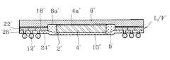
여기서 상기 봉지 단계는 리드프레임(L/F)의 돌출부(26) 저면이 봉지수단(10) 외부로 노출되도록 하여야 하며 상기와 같은 봉지 단계 이후에는 리드프레임(L/F)의 돌출부(26)에 솔더(26a) 도금을 실시하거나 또는 솔더볼(12)을 융착하여 메인보드에로의 신호 입/출력수단으로 사용할 수 있도록 한다. 또한 상기 봉지 단계에서 봉지수단(10)은 에폭시몰딩컴파운드를 사용하거나 또는 액상봉지제를 사용하며 이는 제한적이지 않고 선택적이다.Here, the encapsulation step should be such that the bottom surface of the protruding
한편, 도5a는 상기한 바와 같이 리드프레임(L/F)의 돌출부(26)에 솔더(26a) 도금을 형성하는 대신 종래와 같이 솔더볼(12)을 융착한 상태를 도시한 것이며 도5b는 종래와 동일한 크기의 반도체패키지(PKG)에 보다 더 큰 반도체칩(4)을 안착한 상태를 도시한 것이다. 이와 같이 보다 더 큰 반도체칩(4)이 안착될 수 있기 위해서는 방열판(6)에 형성되는 요부(6a)를 더 크게 하고 또한 와이어본딩 대신에 반도체칩(4)의 범프(14)들과 리드프레임(L/F)의 본드핑거(24)들을 한꺼번에 본딩시키는 갱본딩 방법을 사용함으로서 가능한 것이다.Meanwhile, FIG. 5A illustrates a state in which the
이상에서와 같이 본 발명은 비록 상기의 실시예에 한하여 설명하였지만 여기에만 한정되지 않으며 본 발명의 범주와 사상을 벗어나지 않는 범위내에서 당업자에 의해 여러가지로 변형된 실시예도 가능할 것이다.As described above, although the present invention has been described with reference to the above embodiments, various modifications may be made by those skilled in the art without departing from the scope and spirit of the present invention.
따라서 본 발명에 의하면, 첫째, 종래의 와이어본딩 대신 탭본딩의 한종류인 갱본딩 방법을 이용하여 반도체칩의 입/출력패드와 리드를 직접 범프로 연결함으로써 봉지수단의 두께를 감소시키고 또한 패키지 내의 공간 여유도를 증가시켜 결과적으로 반도체패키지의 두께를 박형화하고 또한 같은 크기의 반도체패키지에 보다 더 큰 반도체칩을 수용할 수 있는 리드프레임을 이용한 반도체패키지를 제공한다.Therefore, according to the present invention, first, by using a gang bonding method, which is a type of tab bonding instead of the conventional wire bonding, by directly connecting the input / output pad and the lead of the semiconductor chip with bumps, the thickness of the sealing means is reduced and the space in the package is also reduced. As a result, the semiconductor package using a lead frame can be provided to increase the margin, thereby reducing the thickness of the semiconductor package and accommodating larger semiconductor chips in the same size semiconductor package.
둘째, 입/출력 수단으로 리드프레임의 돌출부에 솔더 도금을 실시하거나 솔더볼을 융착하여 사용 가능하게 함으로써 그 선택폭을 넓혀 비용 절감을 가능하게 한 리드프레임을 이용한 반도체패키지를 제공한다.Second, it provides a semiconductor package using a lead frame that can reduce the cost by widening the choice by soldering the soldering to the protrusion of the lead frame or by welding the solder ball as an input / output means.
셋째, 반도체칩의 입/출력패드와 리드프레임의 본드핑거 연결 수단을 범프로 함으로써 그 전기적 저항을 크게 감소시켜 반도체칩의 기능을 대폭 향상시킬 수 있는 효과가 있다.Third, by bumping the input / output pad of the semiconductor chip and the bond finger connecting means of the lead frame, the electrical resistance can be greatly reduced, thereby greatly improving the function of the semiconductor chip.
Claims (4)
Translated fromKoreanPriority Applications (1)
| Application Number | Priority Date | Filing Date | Title |
|---|---|---|---|
| KR1019970054507AKR100260996B1 (en) | 1997-10-23 | 1997-10-23 | Array type semiconductor package using a lead frame and its manufacturing method |
Applications Claiming Priority (1)
| Application Number | Priority Date | Filing Date | Title |
|---|---|---|---|
| KR1019970054507AKR100260996B1 (en) | 1997-10-23 | 1997-10-23 | Array type semiconductor package using a lead frame and its manufacturing method |
Publications (2)
| Publication Number | Publication Date |
|---|---|
| KR19990033212A KR19990033212A (en) | 1999-05-15 |
| KR100260996B1true KR100260996B1 (en) | 2000-07-01 |
Family
ID=19523284
Family Applications (1)
| Application Number | Title | Priority Date | Filing Date |
|---|---|---|---|
| KR1019970054507AExpired - Fee RelatedKR100260996B1 (en) | 1997-10-23 | 1997-10-23 | Array type semiconductor package using a lead frame and its manufacturing method |
Country Status (1)
| Country | Link |
|---|---|
| KR (1) | KR100260996B1 (en) |
Cited By (1)
| Publication number | Priority date | Publication date | Assignee | Title |
|---|---|---|---|---|
| KR101259481B1 (en)* | 2011-09-19 | 2013-05-06 | 주식회사 휘닉스소재 | A Heat Sluge having tape improvemented Semiconductor packages of adhesion |
Families Citing this family (2)
| Publication number | Priority date | Publication date | Assignee | Title |
|---|---|---|---|---|
| KR100583494B1 (en)* | 2000-03-25 | 2006-05-24 | 앰코 테크놀로지 코리아 주식회사 | Semiconductor Package |
| KR100488489B1 (en)* | 2002-03-07 | 2005-05-11 | 주식회사 케이이씨 | chip size package and its manufacturing method |
Citations (2)
| Publication number | Priority date | Publication date | Assignee | Title |
|---|---|---|---|---|
| JPH09181209A (en)* | 1995-12-26 | 1997-07-11 | Hitachi Ltd | Semiconductor device and manufacturing method thereof |
| JPH09246427A (en)* | 1996-03-12 | 1997-09-19 | Dainippon Printing Co Ltd | Method for manufacturing surface-mounted semiconductor device and surface-mounted semiconductor device |
- 1997
- 1997-10-23KRKR1019970054507Apatent/KR100260996B1/ennot_activeExpired - Fee Related
Patent Citations (2)
| Publication number | Priority date | Publication date | Assignee | Title |
|---|---|---|---|---|
| JPH09181209A (en)* | 1995-12-26 | 1997-07-11 | Hitachi Ltd | Semiconductor device and manufacturing method thereof |
| JPH09246427A (en)* | 1996-03-12 | 1997-09-19 | Dainippon Printing Co Ltd | Method for manufacturing surface-mounted semiconductor device and surface-mounted semiconductor device |
Cited By (1)
| Publication number | Priority date | Publication date | Assignee | Title |
|---|---|---|---|---|
| KR101259481B1 (en)* | 2011-09-19 | 2013-05-06 | 주식회사 휘닉스소재 | A Heat Sluge having tape improvemented Semiconductor packages of adhesion |
Also Published As
| Publication number | Publication date |
|---|---|
| KR19990033212A (en) | 1999-05-15 |
Similar Documents
| Publication | Publication Date | Title |
|---|---|---|
| KR100260997B1 (en) | Semiconductor package | |
| USRE42653E1 (en) | Semiconductor package with heat dissipating structure | |
| US5684330A (en) | Chip-sized package having metal circuit substrate | |
| US7122401B2 (en) | Area array type semiconductor package fabrication method | |
| US6781242B1 (en) | Thin ball grid array package | |
| JP3526788B2 (en) | Method for manufacturing semiconductor device | |
| US8916958B2 (en) | Semiconductor package with multiple chips and substrate in metal cap | |
| JP2005064479A (en) | Circuit module | |
| US5808872A (en) | Semiconductor package and method of mounting the same on circuit board | |
| US6819565B2 (en) | Cavity-down ball grid array semiconductor package with heat spreader | |
| US7173341B2 (en) | High performance thermally enhanced package and method of fabricating the same | |
| KR100649869B1 (en) | Semiconductor package | |
| KR0179802B1 (en) | Semiconductor package | |
| KR100260996B1 (en) | Array type semiconductor package using a lead frame and its manufacturing method | |
| KR19990024255U (en) | Stacked Ball Grid Array Package | |
| KR100186759B1 (en) | Heat radiating structure of ball grid array semiconductor package using solder ball as input-output | |
| JPH09330994A (en) | Semiconductor device | |
| KR100226106B1 (en) | Ball Grid Array Semiconductor Package Using Lead Frame and Manufacturing Method Thereof | |
| KR100218633B1 (en) | Ball Grid Array Semiconductor Package with Carrier Frame | |
| KR19990056764A (en) | Ball grid array package | |
| KR200172710Y1 (en) | Chip size package | |
| KR100444175B1 (en) | ball grid array of stack chip package | |
| KR100708050B1 (en) | Semiconductor Package | |
| JP3127948B2 (en) | Semiconductor package and mounting method thereof | |
| KR19980046821A (en) | Structure and manufacturing method of ball grid array (BGA) semiconductor package with heat sink |
Legal Events
| Date | Code | Title | Description |
|---|---|---|---|
| A201 | Request for examination | ||
| PA0109 | Patent application | St.27 status event code:A-0-1-A10-A12-nap-PA0109 | |
| PA0201 | Request for examination | St.27 status event code:A-1-2-D10-D11-exm-PA0201 | |
| R17-X000 | Change to representative recorded | St.27 status event code:A-3-3-R10-R17-oth-X000 | |
| R18-X000 | Changes to party contact information recorded | St.27 status event code:A-3-3-R10-R18-oth-X000 | |
| R18-X000 | Changes to party contact information recorded | St.27 status event code:A-3-3-R10-R18-oth-X000 | |
| PN2301 | Change of applicant | St.27 status event code:A-3-3-R10-R13-asn-PN2301 St.27 status event code:A-3-3-R10-R11-asn-PN2301 | |
| PN2301 | Change of applicant | St.27 status event code:A-3-3-R10-R13-asn-PN2301 St.27 status event code:A-3-3-R10-R11-asn-PN2301 | |
| PG1501 | Laying open of application | St.27 status event code:A-1-1-Q10-Q12-nap-PG1501 | |
| N231 | Notification of change of applicant | ||
| PN2301 | Change of applicant | St.27 status event code:A-3-3-R10-R13-asn-PN2301 St.27 status event code:A-3-3-R10-R11-asn-PN2301 | |
| R17-X000 | Change to representative recorded | St.27 status event code:A-3-3-R10-R17-oth-X000 | |
| R18-X000 | Changes to party contact information recorded | St.27 status event code:A-3-3-R10-R18-oth-X000 | |
| E902 | Notification of reason for refusal | ||
| PE0902 | Notice of grounds for rejection | St.27 status event code:A-1-2-D10-D21-exm-PE0902 | |
| P11-X000 | Amendment of application requested | St.27 status event code:A-2-2-P10-P11-nap-X000 | |
| P13-X000 | Application amended | St.27 status event code:A-2-2-P10-P13-nap-X000 | |
| E701 | Decision to grant or registration of patent right | ||
| PE0701 | Decision of registration | St.27 status event code:A-1-2-D10-D22-exm-PE0701 | |
| GRNT | Written decision to grant | ||
| PR0701 | Registration of establishment | St.27 status event code:A-2-4-F10-F11-exm-PR0701 | |
| PR1002 | Payment of registration fee | St.27 status event code:A-2-2-U10-U11-oth-PR1002 Fee payment year number:1 | |
| PG1601 | Publication of registration | St.27 status event code:A-4-4-Q10-Q13-nap-PG1601 | |
| PR1001 | Payment of annual fee | St.27 status event code:A-4-4-U10-U11-oth-PR1001 Fee payment year number:4 | |
| PR1001 | Payment of annual fee | St.27 status event code:A-4-4-U10-U11-oth-PR1001 Fee payment year number:5 | |
| PR1001 | Payment of annual fee | St.27 status event code:A-4-4-U10-U11-oth-PR1001 Fee payment year number:6 | |
| PR1001 | Payment of annual fee | St.27 status event code:A-4-4-U10-U11-oth-PR1001 Fee payment year number:7 | |
| PR1001 | Payment of annual fee | St.27 status event code:A-4-4-U10-U11-oth-PR1001 Fee payment year number:8 | |
| PR1001 | Payment of annual fee | St.27 status event code:A-4-4-U10-U11-oth-PR1001 Fee payment year number:9 | |
| PR1001 | Payment of annual fee | St.27 status event code:A-4-4-U10-U11-oth-PR1001 Fee payment year number:10 | |
| PR1001 | Payment of annual fee | St.27 status event code:A-4-4-U10-U11-oth-PR1001 Fee payment year number:11 | |
| PR1001 | Payment of annual fee | St.27 status event code:A-4-4-U10-U11-oth-PR1001 Fee payment year number:12 | |
| PR1001 | Payment of annual fee | St.27 status event code:A-4-4-U10-U11-oth-PR1001 Fee payment year number:13 | |
| FPAY | Annual fee payment | Payment date:20130411 Year of fee payment:14 | |
| PR1001 | Payment of annual fee | St.27 status event code:A-4-4-U10-U11-oth-PR1001 Fee payment year number:14 | |
| FPAY | Annual fee payment | Payment date:20140410 Year of fee payment:15 | |
| PR1001 | Payment of annual fee | St.27 status event code:A-4-4-U10-U11-oth-PR1001 Fee payment year number:15 | |
| PR1001 | Payment of annual fee | St.27 status event code:A-4-4-U10-U11-oth-PR1001 Fee payment year number:16 | |
| FPAY | Annual fee payment | Payment date:20160412 Year of fee payment:17 | |
| PR1001 | Payment of annual fee | St.27 status event code:A-4-4-U10-U11-oth-PR1001 Fee payment year number:17 | |
| LAPS | Lapse due to unpaid annual fee | ||
| PC1903 | Unpaid annual fee | St.27 status event code:A-4-4-U10-U13-oth-PC1903 Not in force date:20170415 Payment event data comment text:Termination Category : DEFAULT_OF_REGISTRATION_FEE | |
| PC1903 | Unpaid annual fee | St.27 status event code:N-4-6-H10-H13-oth-PC1903 Ip right cessation event data comment text:Termination Category : DEFAULT_OF_REGISTRATION_FEE Not in force date:20170415 | |
| PN2301 | Change of applicant | St.27 status event code:A-5-5-R10-R13-asn-PN2301 St.27 status event code:A-5-5-R10-R11-asn-PN2301 | |
| P22-X000 | Classification modified | St.27 status event code:A-4-4-P10-P22-nap-X000 |