KR100258292B1 - Picture display device - Google Patents
Picture display deviceDownload PDFInfo
- Publication number
- KR100258292B1 KR100258292B1KR1019970704545AKR19970704545AKR100258292B1KR 100258292 B1KR100258292 B1KR 100258292B1KR 1019970704545 AKR1019970704545 AKR 1019970704545AKR 19970704545 AKR19970704545 AKR 19970704545AKR 100258292 B1KR100258292 B1KR 100258292B1
- Authority
- KR
- South Korea
- Prior art keywords
- image display
- display panel
- array
- micro
- micro lens
- Prior art date
- Legal status (The legal status is an assumption and is not a legal conclusion. Google has not performed a legal analysis and makes no representation as to the accuracy of the status listed.)
- Expired - Fee Related
Links
Images


Classifications
- G—PHYSICS
- G02—OPTICS
- G02F—OPTICAL DEVICES OR ARRANGEMENTS FOR THE CONTROL OF LIGHT BY MODIFICATION OF THE OPTICAL PROPERTIES OF THE MEDIA OF THE ELEMENTS INVOLVED THEREIN; NON-LINEAR OPTICS; FREQUENCY-CHANGING OF LIGHT; OPTICAL LOGIC ELEMENTS; OPTICAL ANALOGUE/DIGITAL CONVERTERS
- G02F1/00—Devices or arrangements for the control of the intensity, colour, phase, polarisation or direction of light arriving from an independent light source, e.g. switching, gating or modulating; Non-linear optics
- G02F1/01—Devices or arrangements for the control of the intensity, colour, phase, polarisation or direction of light arriving from an independent light source, e.g. switching, gating or modulating; Non-linear optics for the control of the intensity, phase, polarisation or colour
- G02F1/13—Devices or arrangements for the control of the intensity, colour, phase, polarisation or direction of light arriving from an independent light source, e.g. switching, gating or modulating; Non-linear optics for the control of the intensity, phase, polarisation or colour based on liquid crystals, e.g. single liquid crystal display cells
- G02F1/133—Constructional arrangements; Operation of liquid crystal cells; Circuit arrangements
- G02F1/1333—Constructional arrangements; Manufacturing methods
- G02F1/1335—Structural association of cells with optical devices, e.g. polarisers or reflectors
- G02F1/133526—Lenses, e.g. microlenses or Fresnel lenses
Landscapes
- Physics & Mathematics (AREA)
- Nonlinear Science (AREA)
- Mathematical Physics (AREA)
- Chemical & Material Sciences (AREA)
- Crystallography & Structural Chemistry (AREA)
- General Physics & Mathematics (AREA)
- Optics & Photonics (AREA)
- Liquid Crystal (AREA)
- Devices For Indicating Variable Information By Combining Individual Elements (AREA)
Abstract
Translated fromKoreanDescription
Translated fromKorean서두에서 언급된 형태의 영상 표시장치는 예를들면 JP-A-5-346578의 영어 요약서에 공지되어 있다. 상기 요약서에 기재된 영상 표시장치는 매트릭스내에 정렬된 다수의 화소를 포함하는 전달 액정 영상표시 패널을 구비한다. 제 1 마이크로 렌즈 어레이는 영상 표시 패널의 조명쪽에 정렬되고, 제 2 마이크로 어레이는 상기 조명쪽으로부터 이격된 영상 표시 패멸의 쪽에 정렬된다. 상기 2개의 마이크로 렌즈 어레이의 초점길이는 상기 각각의 마이크로 렌즈 어레이와 영상 표시 패널사이의 거리와 거의 동일하다. 또한, 상기 제 2 마이크로 렌즈 어레이위에서 제 1 마이크로 렌즈 어레이를 투영하는 제 3 마이크로 렌즈 어레이는 상기 영상 표시 패널에 근접하게 정렬된다.An image display device of the type mentioned at the outset is known, for example, in the English abstract of JP-A-5-346578. The image display device described in the above summary comprises a transfer liquid crystal image display panel comprising a plurality of pixels arranged in a matrix. The first micro lens array is aligned with the illumination side of the image display panel, and the second micro array is aligned with the side of the image display panel spaced apart from the illumination side. The focal length of the two micro lens arrays is approximately equal to the distance between each of the micro lens arrays and the image display panel. In addition, a third micro lens array projecting the first micro lens array on the second micro lens array is aligned in close proximity to the image display panel.
마이크로 렌즈 어레이는 영상 표시패널의 제한된 개구로 인한 손실을 감소시키기 위하여, 액정 영상 표시패널을 포함하는 영상 표시 장치에 사용된다는 것은 공지되어 있다. 상기 목적을 위하여, 조명 시스템과, 마이크로 렌즈 어레이 및 영상 표시 패널은 상기 마이크로 렌즈 어레이의 렌즈위에 조사되는 비임이 대응되는 화소의 활성부위에 포커스되는 방법으로 서로에 대하여 위치되는 것이 양호하다. 단점은 상기 조사비임이 발산될 때, 상기 비임부분이 제 2 마이크로 렌즈 어레이의 대응하는 렌즈위에 더 이상 조사되지 않을것이고, 상기 빛은 2개이상의 인접된 렌즈를 가로질러 분포될 것이다. 상기와 같은 혼선은 출력을 증가시키고, 영상의 질을 감소시킬 것이다.It is known that the micro lens array is used in an image display apparatus including a liquid crystal image display panel in order to reduce the loss due to the limited opening of the image display panel. For this purpose, the illumination system, the micro lens array and the image display panel are preferably positioned relative to each other in such a way that the beam irradiated onto the lens of the micro lens array is focused on the active portion of the corresponding pixel. The disadvantage is that when the irradiation beam is diverged, the beam portion will no longer be irradiated on the corresponding lens of the second micro lens array and the light will be distributed across two or more adjacent lenses. Such crosstalk will increase output and reduce image quality.
상기 요약서에 기재된 영상 표시패널과 일체로 되는 마이크로 렌즈 어레이는 영상 표시 패널에 수직이 아닌 주 광선(chief ray)을 가진 비임이 이것의 빛이 조명되는 인접 렌즈가 없이 제 2 마이크로 렌즈 어레이의 대등되는 렌즈에만 도달할 수 있는 방법으로 굴절되는 것을 보장한다. 이러한 방법에서, 인접된 렌즈사이에 대한 혼선은 가능한 많이 피해야만 하고, 이것은 투영 렌즈 시스템의 요구되는 개구와 영상질에 공헌하게 된다.The microlens array, which is integrated with the image display panel described in the above summary, has a beam having a chief ray that is not perpendicular to the image display panel so that the second micro lens array is comparable without the adjacent lens to which its light is illuminated. It ensures refraction in a way that only the lens can be reached. In this way, crosstalk between adjacent lenses should be avoided as much as possible, which contributes to the required aperture and image quality of the projection lens system.
상기 요약서로 부터 공지된 영상 표시장치의 단점은 상기 제 3 마이크로 렌즈 어레이가 영상 표시 패널의 LC 물질에 매우 근접되게 정렬된다는 것이다. 상기 렌즈가 이온 교환에 의해 LC 물질 기판중의 하나 또는 둘다에서 굴절율 변화에 의하여 구성된다면, 상기 관련된 기판은 알카리 이온을 포함해야만 한다. 상기 경우에, LC 물질은 이온 교환 방법에 의하여 오염될 것이라는 큰 위험이 있게 된다. 상기 이온교환의 결과로써, 기판은 서로다른 굴절율을 가질 것이다. 이러한 점은 큰 온도변화에서 액정층의 균일한 두께를 실현시키는 것을 매우 어렵게 하는데, 왜냐하면 서로다른 굴절율을 가진 기판이 서로 다른 열팽창 계수를 가지기 때문이다. 상술된 현상의 결과로써, 상기 마이크로 렌즈 구조체가 LC 물질에 근접된 기판의 내부쪽에 정렬된다면, 만족스러운 영상의 질을 성취하는 것은 매우 어렵다.A disadvantage of the image display device known from the above summary is that the third micro lens array is aligned very close to the LC material of the image display panel. If the lens is constituted by a refractive index change in one or both of the LC material substrates by ion exchange, the associated substrate must contain alkali ions. In this case, there is a great risk that the LC material will be contaminated by the ion exchange method. As a result of the ion exchange, the substrate will have different refractive indices. This makes it very difficult to realize a uniform thickness of the liquid crystal layer at a large temperature change, because substrates having different refractive indices have different coefficients of thermal expansion. As a result of the above-described phenomenon, it is very difficult to achieve satisfactory image quality if the micro lens structure is aligned inside the substrate in proximity to the LC material.
전달 영상 표시 패널을 가진 영상 표시 장치용으로써 상술된 바와 같은 문제점은 굴절 영상 표시패널을 가진 영상 표시 장치에서 그 자체로써 존재하고, 이것은 투영 렌즈 시스템을 향하여 빛을 전달하는 마이크로 렌즈의 인접된 렌즈사이의 혼선을 감소시키기 위하여 취해진다. 굴절 영상 표시 패널을 가진 영상 표시 장치에서, 마이크로 렌즈 어레이는 영상 표시 패널의 조명쪽에 정렬된다. 상기 동일한 마이크로 렌즈 어레이는 상기 영상 표시 패널에 의하여 조절되는 빛이 투영 렌즈 시스템을 향하여 전달되는 것을 보장한다. 전달 영상 표시 패널을 가진 영상 표시 장치와 유사하게, LC 물질에 대향되는 상기 기판쪽에서 기판을 가지고 마이크로 렌즈 어레이와 일체로 되는 것은 매우 어렵고, 상기 마이크로 렌즈 어레이는 상기 조절된 비임이 마이크로 렌즈 어레이중의 단지 하나의 렌즈위에 조사되는 것을 보장한다.The problem as described above for an image display device with a delivery image display panel is present in itself in an image display device with a refractive image display panel, which is between adjacent lenses of the microlenses that transmit light towards the projection lens system. Is taken to reduce crosstalk. In an image display apparatus having a refractive image display panel, the micro lens array is aligned with the illumination side of the image display panel. The same micro lens array ensures that light controlled by the image display panel is directed towards the projection lens system. Similar to an image display device having a transfer image display panel, it is very difficult to integrate a microlens array with a substrate on the substrate side opposite the LC material, the microlens array wherein the controlled beam of the microlens array Ensure that only one lens is irradiated.
본 말명은 조명 시스템과, 화소(pixel)의 매트릭스를 가진 전달 영상 표시패널과, 상기 영상 표시패널의 조명쪽에 있고 렌즈수는 영상 표시패널의 화소수에 대응되는 제 1 마이크로 렌즈 어레이와, 상기 조명 시스템으로 부터 이격되는 영상 표시패널쪽에 있고 렌즈수는 영상 표시패널의 화소수에 대응되는 제 2 마이크로 렌즈 어레이를 포함하고, 비임 굴절 수단과 투영 렌즈 시스템을 부가로 포함하는 영상 표시장치에 관한 것이다.The present invention refers to an illumination system, a delivery image display panel having a matrix of pixels, a first micro lens array on the illumination side of the image display panel, the number of lenses corresponding to the number of pixels of the image display panel, and the illumination. The image display panel is located on an image display panel spaced apart from the system, and the number of lenses includes a second micro lens array corresponding to the number of pixels of the image display panel, and further includes a beam refraction means and a projection lens system.
제1도는 전달성 영상 표시 패널의 양쪽에서 마이크로 렌즈 어레이를 구비하는 상 투영 장치의 실시예를 도시하는 도면.1 shows an embodiment of an image projector having micro lens arrays on both sides of a transferable image display panel.
제2a도 및 제2b도는 영상 표시 패널의 화소와 관련되는 방사경로가 완전히 평행으로 된 비임과, 작은 발산을 가지는 비임으로 부터의 광선을 위하여 도시되는 전달성 영상 표시 패널을 가지는, 본 발명에 따른 영상 표시 장치의 부분의 2개의 실시예를 도시하는 도면.2a and 2b have a beam in which the radiation paths associated with the pixels of the image display panel are completely parallel and a transmissive image display panel shown for the light rays from the beam with small divergence, according to the invention Fig. 2 shows two embodiments of parts of the video display device.
제3a도 및 제3b도는 영상 표시 패널의 화소와 관련되는 방사경로가 완전히 평행한 비임과, 작은 발산을 가지는 비임으로 부터의 광선을 위하여 도시되는 반사성 영상 표시 패널을 가지는, 본 발명에 따른 영상 표시 장치의 부분의 2개의 실시예를 도시하는 도면.3A and 3B show an image display according to the present invention, having a beam in which the radiation paths associated with the pixels of the image display panel are completely parallel and a reflective image display panel shown for light rays from a beam having a small divergence. Figure 2 shows two embodiments of parts of the device.
제4도는 합성 어레이에서 마이크로 렌즈와 마이크로 프리즘의 조합이 실현될 수 있는 몇몇 가능성을 도시하는 도면.4 shows some possibilities in which a combination of micro lenses and micro prisms can be realized in a composite array.
본 발명의 목적은 조명 시스템과 투영 렌즈 시스템사이의 광 경로의 출력이 유지되는 영상 표시장치를 제공함으로써, 투영 렌즈의 개구가 제한되게 남아있을 수 있도록 하는 것이다. 상기 영상 표시 장치는 상기 목적이 관찰되는 상술되고 공지된 영상 표시 장치보다 더 쉽게 제조될 수 있다. 본 발명에 따른 영상 표시장치는 영상 표시 패널의 작동이 확산을 기초로 할 때, 관련되는 출력을 유지할수 있는 한 특히 많은 장점을 가진다.It is an object of the present invention to provide an image display device in which the output of the optical path between the illumination system and the projection lens system is maintained, so that the opening of the projection lens can remain limited. The image display device can be manufactured more easily than the above-mentioned and known image display device in which the object is observed. The video display device according to the invention has particular advantages as long as the operation of the video display panel is based on diffusion, as long as it can maintain the associated output.
상술된 목적을 성취하기 위한 본 발명에 따라 제안되는 원리는 전달성 및 반사성 영상 표시 패널 둘다의 영상 표시 장치에 적용가능하다. 굴절성 영상 표시 패널을 가진 영상 표시 장치와, 전달성 영상 표시 패널을 가진 영상 표시 장치사이에서 구조상의 차이는 사용되는 영상 표시 패널의 형태의 자동적인 결과이다.The principle proposed in accordance with the present invention for achieving the above-mentioned object is applicable to an image display apparatus of both a transmissive and a reflective image display panel. The structural difference between the image display apparatus having the refractive image display panel and the image display apparatus having the transferable image display panel is an automatic result of the form of the image display panel used.
본 발명에 따른 영상 표시 장치의 제 1 실시예는 하나의 마이크로 렌즈 어레이의 렌즈 초점길이부가 다른 마이크로 렌즈 어레이에 위치되고, 그리고 그 반대로 될 수 있으며 상기 비임 굴절 수단은 상기 제 1 마이크로 렌즈 어레이 및 제 1 비임 굴절 어레이와, 제 2 마이크로 렌즈 어레이 및 비임 굴절 요소가 각 마이크로 렌즈에 대응되는 제 2 비임 굴절 어레이를 위하여 유지하면서 제 1 및 제 2 비임 굴절 어레이에 의하여 구성되며, 상기 비임 굴절 어레이는 영상 표시 패널의 영역에서 비임 웨이스팅 효과(beam-waisting effect)를 가지는 것을 특징으로 한다.In a first embodiment of the image display device according to the present invention, the lens focal length portion of one micro lens array may be located on another micro lens array, and vice versa, and the beam refraction means may include the first micro lens array and the first micro lens array. The first and second beam deflection arrays are constructed by maintaining a first beam deflection array, a second micro lens array and a beam deflection element for a second beam deflection array corresponding to each micro lens, the beam deflection array being an image. And a beam-waisting effect in an area of the display panel.
상기 마이크로 렌즈 어레이는 마이크로 렌즈로써 광학적으로 동일한 작용을 가지는 흘로그래픽(holographic) 광학 요소를 포함하는 종래의 마이크로 렌즈 어레이 또는 어레이들이 될 수 있다.The microlens array may be a conventional microlens array or arrays comprising holographic optical elements having optically the same function as the microlenses.
상기 2개의 마이크로 렌즈 어레이는 서로의 초점에 있다. 상기 제 2 마이크로 렌즈 어레이의 마이크로 렌즈위에 포커스함으로써, 상기 제 1 마이크로 렌즈 어레이의 렌즈위의 어떤 각도에서 조사되는 비임은 제 2 마이크로 렌즈 어레이의 단지 하나의 렌즈에 도달함으로써, 인접된 렌즈사이의 문제점은 상당히 감소된다. 상기 영상 표시 패널의 영역에서, 비임 굴절 요소를 가진 어레이는 화소의 중심주위에서 웨이스트됨으로써, 상기 비임의 대부분은 화소의 활성부분에 자동적으로 도달한다. 또한, 상기 장치의 출력은 거의 일정하고, 동일한 영상질을 유지하기 위하여 투영 렌즈 시스템의 개구의 확대부를 요구하지 않는다. 상기 비임 굴절 요소는 LC 물질에 근접된 기판의 내부쪽에 더 이상 존재하지 않지만, 예를 들면 기판의 외부쪽에 존재하거나, 또는 분리된 요소를 구성하기 때문에, 상기 장치의 제조는 상당히 간략하게된다. 상기 비임 굴절 요소는 마이크로 렌즈와 일체로 되는 것이 양호하다. 그래서 자유면의 수는 제한되고, 불필요한 반사손실은 피할 수 있다.The two micro lens arrays are in focus with each other. By focusing on the microlenses of the second microlens array, the beam irradiated at any angle on the lenses of the first microlens array reaches only one lens of the second microlens array, thereby causing problems between adjacent lenses. Is significantly reduced. In the area of the image display panel, the array with the beam refracting elements is waisted around the center of the pixel so that most of the beam automatically reaches the active portion of the pixel. In addition, the output of the device is almost constant and does not require an enlargement of the opening of the projection lens system to maintain the same image quality. The beam refracting element is no longer present on the inside of the substrate in proximity to the LC material, but, for example, on the outside of the substrate or constitutes a separate element, the manufacture of the device is quite simplified. Preferably, the beam refracting element is integrated with the micro lens. Thus, the number of free surfaces is limited and unnecessary return loss can be avoided.
본 발명에 따른 영상 표시 장치의 제 2 실시예는 마이크로 렌즈 어레이중의 하나의 렌즈의 초점길이부는 동일한 마이크로 어레이중의 하나의 렌즈에 위치되고, 상기 비임 굴절 수단은 이것이 마이크로 렌즈 어레이와, 비임 굴절 요소가 각각의 마이크로 렌즈에 대응되는 비임 굴절 어레이를 위하여 유지되면서 비임 굴절 어레이에 의하여 구성되고, 상기 비임 굴절 어레이는 영상 표시 패널의 영역에서 비임 웨이스팅 효과를 가진다.According to a second embodiment of the image display apparatus according to the present invention, the focal length portion of one lens of the micro lens array is located in one lens of the same micro array, and the beam refraction means means that this is a micro lens array and a beam refraction. An element is constituted by the beam refraction array while being maintained for the beam refraction array corresponding to each micro lens, the beam refraction array having a beam waisting effect in the region of the image display panel.
상기 실시예에서, 영상 표시 패널은 반사 영상 표시 패널이다. 상기 경우에, 상기 장치는 조명 시스템과 영상 표시 패널사이에 정렬된 단지 하나외 마이크로 렌즈 어레이를 포함한다. 상기 어레이의 렌즈 초점은 어레이 그 자체에 위치됨으로써, 상기 초점길이는 마이크로 렌즈 어레이와 영상 표시 패널사이의 거리에 두배와 거의 동일하다. 비임 굴절요소는 상기 마이크로 렌즈 어레이의 각각의 렌즈에 대응된다. 상기 비임 굴절 요소의 어레이는 마이크로 렌즈 어레이와 일체로 되는 것이 양호하다. 상기 마이크로 렌즈 어레이의 렌즈위에 조사되는 조명 시스템으로 부터의 비임은 영상 표시 패널의 영역에서 웨이스트되고, 반사이후에 다시 마이크로 렌즈 어레이로 전달되고, 여기에서 이것은 예를 들면 전진 경로의 렌즈와 동일한 렌즈에서 포커스된다. 상기 마이크로 렌즈 어레이와 영상 표시 패널의 상대위치와, 비임 굴절요소에 의한 영상 표시 패널의 영역에서의 비임 웨이스트로 인하여, 상기 비임의 보다 큰 부분은 마이크로 렌즈에 대응되는 화소의 활성부 위에 자동적으로 조사될 것이다.In the above embodiment, the image display panel is a reflective image display panel. In this case, the device comprises only one extra micro lens array arranged between the illumination system and the image display panel. The lens focal point of the array is located in the array itself so that the focal length is approximately equal to twice the distance between the micro lens array and the image display panel. The beam refracting element corresponds to each lens of the micro lens array. The array of beam refracting elements is preferably integrated with the micro lens array. The beam from the illumination system irradiated onto the lens of the micro lens array is wasted in the area of the image display panel, and after reflection is transferred back to the micro lens array, where it is for example in the same lens as the lens in the forward path. It is focused. Due to the relative position of the microlens array and the image display panel and the beam waste in the region of the image display panel by the beam refraction element, a larger portion of the beam is automatically irradiated onto the active portion of the pixel corresponding to the microlens. Will be.
상술된 2개의 실시예에서, 영상 표시장치에서의 출력은 강도를 유지하면서 유지되고, 마이크로 렌즈 어레이의 인접된 렌즈 사이의 혼선의 위험을 통하여 투영렌즈 시스템으로 보내어지는 조절되는 빛은 상당히 감소된다.In the two embodiments described above, the output at the image display device is maintained while maintaining the intensity, and the controlled light sent to the projection lens system through the risk of crosstalk between adjacent lenses of the micro lens array is significantly reduced.
본 발명에 따른 영상 표시장치의 양호한 실시예는 비임 굴절요소가 하나이상의 크기에서 적어도 2개 이상의 평면을 가지는 마이크로 프리즘이다.A preferred embodiment of the image display device according to the invention is a micro prism in which the beam refracting element has at least two or more planes in one or more sizes.
상기 실시예에서, 마이크로 프리즘은 각각의 마이크로 렌즈 어레이의 각각의 렌즈와 관련된다. 상기 프리즘 그자체는 어떠한 부가의 발산을 도입하지 않는다. 상기 마이크로 렌즈는 조사된 비임을 포커스시키고, 상기 마이크로 프리즘은 영상 표시 패널의 영역에서 비임을 웨이스트하고, 투영 렌즈 시스템을 향하여 조절되는 비임을 전달하는 마이크로 렌즈 어레이의 바람직한 렌즈를 향하도록 한다.In this embodiment, the micro prisms are associated with each lens of each micro lens array. The prism itself does not introduce any additional divergence. The microlenses focus the irradiated beam, and the microprism is directed to the desired lens of the microlens array which wastes the beam in the area of the image display panel and delivers the beam adjusted towards the projection lens system.
하나의 크기에서의 평면의 수는 프리즘이 서로 연속되는 방향에서 영상 표시 패널의 영역에서 웨이스트되는 요소를 결정한다. 2개의 평면을 위하여, 영상 표시 패널의 영역에서의 비임 직경은 반으로 감소되는 반면에, 광의 세기를 유지시킨다. 하나의 방향에서의 감소는 충분할 수 있는데, 왜냐하면 수직 및 수평방향에서의 개구가 동일하게 되지 않아야만 하기 때문이다.The number of planes in one size determines the elements that are waste in the area of the image display panel in the direction in which the prisms are continuous with each other. For the two planes, the beam diameter in the area of the image display panel is reduced in half, while maintaining the intensity of the light. The reduction in one direction may be sufficient because the openings in the vertical and horizontal directions should not be the same.
본 발명에 따른 영상 표시 장치의 부가의 실시예는 마이크로 프리즘 어레이의 프리즘은 제 1 크기에서 m 평면과, 제 2 크기에서 n 평면를 가지고, 여기에서 m 과 n은 정수이다.A further embodiment of the image display device according to the invention is that the prism of the micro-prism array has an m plane in the first size and an n plane in the second size, where m and n are integers.
2개의 치수에서 프리즘 평면을 제공함으로써, 상기 개구는 2개의 치수로 영향을 받을수 있다. 소정의 방향에서의 평면의 수는 상기 방향에서의 개구가 감소되는 요소를 결정한다.By providing a prism plane in two dimensions, the opening can be affected in two dimensions. The number of planes in a given direction determines the element by which the opening in that direction is reduced.
본 발명에 따른 영상 표시장치의 부가의 실시예는 소정의 방향에서 나란히 연장되는 적어도 2개의 렌즈 요소로 구성되는 비임 굴절 요소를 특징으로 한다.A further embodiment of the image display device according to the invention features a beam refracting element consisting of at least two lens elements extending side by side in a predetermined direction.
또한, 비임 굴절 요소는 다수의 렌즈로 구성될 수 있다. 소정의 방향에서 나란히 연장되는 다수의 렌즈는 상기 방향에서의 비임이 영상 표시 패널의 영역에서 웨이스트되는 요소에 결정적이다.In addition, the beam refracting element may be comprised of multiple lenses. Many lenses extending side by side in a predetermined direction are critical to the element where the beam in that direction is waste in the area of the image display panel.
반사성 영상 표시 패널이 사용된다면, 이것의 작동은 조사되는 비임의 극성 상태의 조절에 기초로 하며, 상기 조명 시스템으로 부터의 비임과, 상기 영상 표시 패널에 의하여 조절되는 비임은 이들이 극성상태에서 구별될 수 있기 때문에 일치 될 수 있다.If reflective image display panels are used, their operation is based on the adjustment of the polarity state of the beam to be irradiated, and the beams from the illumination system and the beams controlled by the image display panel can be distinguished in their polarity state. Because it can be matched.
상기 반사성 영상 표시 패널의 작동이 예를 들면 PDLC(polymer dispersed liquid crystal; 중합체가 분산된 액정)에서와 같은 조사비임의 확산을 기초로 한다면, 조명 시스템으로 부터의 광비임과, 영상 표시 패널에 의한 영상정보로 조절되는 광비임은 일치하지 않는다는 점에 주의를 해야만 한다. 상기 목적을 위하여, 본 발명에 따른 영상 표시장의 부가의 실시예는 마이크로 렌즈 어레이와 영상 표시 패널이 서로에 대하여 1/2 n.pp의 거리로 오프셋되고, 여기에서 PP는 영상 표시 패널의 피치이고, n은 정수이다If the operation of the reflective image display panel is based on the diffusion of the irradiation beam, for example in a polymer dispersed liquid crystal (PDLC), the light beam from the illumination system and the image by the image display panel. It should be noted that the light beams controlled by information do not match. For this purpose, a further embodiment of the image display field according to the invention is that the microlens array and the image display panel are offset by a distance of 1/2 npp with respect to each other, where PP is the pitch of the image display panel. , n is an integer
결과적으로, 영상 표시패널에 의하여 조절되는 비임은 화소위에 조사되는 비임이 발생되는 곳을 통한 렌즈와는 다른 마이크로 렌즈 어레이의 서로 다른 렌즈에 도달한다. n=1이라면, 상기 조절되는 비임은 조사되는 비임을 통과하는 렌즈에 인접된 렌즈위에 조사한다. 상기 방법에서, 조절되지 않는 비임과 조절되는 비임은 서로로 부터 공간적으로 분리되고, 결과적으로 구별될 수 있다.As a result, the beam controlled by the image display panel reaches different lenses of the micro lens array different from the lens through where the beam irradiated onto the pixel is generated. If n = 1, the adjusted beam is irradiated onto the lens adjacent to the lens passing through the irradiated beam. In this method, the uncontrolled beam and the controlled beam can be spatially separated from each other and as a result can be distinguished.
본 발명에 따른 영상 표시장치의 부가의 실시예는 영상 표시패널과, 비임 굴절 요소와, 마이크로 렌즈 어레이 또는, 상기 제 1 및 제 2 마이크로 렌즈 어레이는 텔레센트릭 형상(telecentric configuration)으로 정렬된다.A further embodiment of the image display device according to the invention is an image display panel, a beam refracting element, a micro lens array or the first and second micro lens arrays are arranged in a telecentric configuration.
그럼으로써, 마이크로 렌즈 어레이의 마이크로 렌즈와 영상 표시 패널의 화소의 상대위치는 영상 표시 패널위의 위치에 독립적이다.Thereby, the relative position of the micro lens of the micro lens array and the pixel of the image display panel is independent of the position on the image display panel.
본 발명의 상기 특징과 다른 특징은 이후에 설명되는 실시예를 참고로 하여 보다 상세하게 설명된다.The above and other features of the present invention will be described in more detail with reference to the embodiments described later.
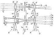
제1도에 개략적으로 도시된 영상 표시 장치(1)는 광 비임(b)를 공급하기 위한 조명 시스템(3)을 포함한다. 상기 광 비임(b)은 간략하게 도시하기 위하여 단일의 콘덴서 렌즈에 의하여 도시되는 콘덴서 렌즈 시스템(5)을 거쳐서 영상 표시 패널(7)워에 조사된다. 상기 영상 표시 패널(7)에 의하여 조절되는 광은 간략하게 도시하기 위하여 단일의 투영 렌즈에 의하여 도시되는 투영 렌즈 시스템(9)으로 투영을 위하여 통과된다.The
상기 조명 시스템(3)은 예를 들면 광원(l5)과 구형 반사기(17)로 구성된다. 상기 반사기(17)는 콘덴서 렌즈(5)로 부터 이격된 방향에서 광원(15)에 의하여 발산되는 광의 보다 큰 부분이 상기 콘덴서 렌즈(5)로 전달되는 것을 보장한다.The
상기 영상 표시 패널(7)은 예를 들면 액정 물질과 화소의 매트릭스를 포함할 수 있고, 이것의 작동은 표시되는 영상정보에 따라서 조사되는 광의 극성방향을 조절할 수 있도록 트위스트된 네마틱(twisted nematic; TN), 수퍼 트위스트된 네마틱(super twisted-nematic; STN)또는, 페로-전기효과(ferro-electric effect)를 기초로 한다. 한편, 상기 영상 표시 패널의 작동은 예를 들면 중합체로 분산된 액정(PDLC)과 같은 조사되는 비극성 광의 발산을 기초로할수 있다. 상기 모든 경우에서, 액정 물질(11)의 충은 예를 들면 유리 또는 인공물질과 같은 2개의 광학적으로 투명한 기판사이에서 제공된다.The
액정 영상 표시 패널은 활성 및 수동성 부분을 포함하는 다수의 화소로 분할 된다. 화소당 상기 활성 및 수동성사이의 비는 영상 표시 패널의 개구를 형성한다. 한정된 개구로 인하여, 광손실은 액정 영상 표시 패널을 가진 영상 표시 장치에서 고려될 수 있다. 이러한 이유로 인하여, 마이크로 렌즈 어레이(19)는 영상표시 패널(7)의 활성 부분위에서 광원(15)으로 부터 광의 최대량을 집중시킬 수 있도록 상기 조명 시스템(3)과 영상 표시 패널(7)사이의 광경로에 종종 사용된다. 그러나, 상기 영상 표시 패널을 통과하거나 그 위에서 반사된 후에, 광비임의 발산과 상기 장치의 효과적인 출력은 상당히 증가할것이다. 보다 큰 개구를 가진 투영 렌즈를 요구하고, 이것은 보다 큰 비용을 요구하게 된다. 특히 확산되는 영상 표시 패널을 가진 시스템에서, 상기 출력의 증가는 매우 불리하게 되는데, 왜냐하면 상기 마이크로 렌즈 어레이와 영상 표시 패뎔은 쉴리렌 광학 시스템(Schlieren optical system)외 중간에 있기 때문이다. 결과적으로, 상기 대조와 휘도는 비임 질의 감소로 인하여 매우 많이 영향을 받게 되는데, 왜냐하면 상기 2개의 비임 질은 렌즈 개구에 의하여 결정되기 때문이다. 공지된 많은 장치에 있어서, 마이크로 렌즈 어레이의 초점길이는 마이크로 렌즈 어레이와 영상 표시 패널 사이의 거리와 거의 동일하다.The liquid crystal image display panel is divided into a plurality of pixels including active and passive portions. The ratio between the active and passivity per pixel forms the opening of the image display panel. Due to the limited aperture, light loss can be considered in an image display device having a liquid crystal image display panel. For this reason, the
상기 광 비임의 발산을 감소시키기 위하여, 상기 장치의 합성의 효과적인 출력은 증가되고, 제 2 마이크로 렌즈 어레이(21)는 마이크로 렌즈 어레이와 영상 표시 패널사이의 거리와 거의 동일한 초점길이를 가지고, 영상 표시 패널(7)뒤에 종종 정렬된다. 양쪽에 마이크로 렌즈 어레이를 가진 영상 표시 패널의 예는 예를 들면, 유럽특허출원 제 0 440 495호에 기재되어 있다.In order to reduce the divergence of the light beam, the effective output of the synthesis of the device is increased, and the second
상기 영상 표시 패널이 반사성 영상 표시 패널이라면, 하나의 마이크로 렌즈 어레이(23)는 조명 시스템(3)과, 영상 표시 패널의 활성부분위에 조사된 비임을 집중시키는 영상 표시 패널(7)사이에 존재하고, 상기 비임이 투영 렌즈 시스템에 도달하기 전에 영상 표시 패널로 부터 조절된 비임을 집중시킨다.If the image display panel is a reflective image display panel, one
상기 조절된 광을 집증시키는 마이크로 렌즈 어레이의 2개 이상의 마이크로 렌즈사이에서 부터 상기 제 1 마이크로 렌즈 어레이의 마이크로 렌즈위에 조사되는 광이 분할되는 것을 방지하기 위하여, 비임 굴절 수단은 제공되어야만 한다. 이러한 점은 예를 들면 영상 표시 패널의 LC 물질에 근접된 마이크로 렌즈 어레이를 정렬함으로써. 예를 들면 JP-A 5-346578의 영어 요약서에 기재된 바와같이, LC 물질의 기판중의 하나의 내부쪽과 일체시킴으로써 실현될 수 있다.A beam refracting means must be provided to prevent splitting of the light irradiated onto the microlenses of the first microlens array from between two or more microlenses of the microlens array which collects the adjusted light. This is achieved by aligning the microlens array in proximity to the LC material of the image display panel, for example. It can be realized by integrating with the inner side of one of the substrates of the LC material, as described, for example, in the English abstract of JP-A 5-346578.
본 발명은 다른 가능성을 제안하는데, 여기에서 전달성 영상 표시 패널의 경우에서의 2개의 마이크로 롄즈 어레이와, 반사성 영상 표시 패널의 경우의 하나의 마이크로 렌즈 어레이를 가진 영상 표시 장치의 출력은 상기 조명 시스템과 투영렌즈 시스템사이의 광경로에서 유지되고, 또한 상기 광의 세기가 유지되며. 그러므로 상기 장치는 매우 간단한 방법으로 제조될 수 있다.The present invention proposes another possibility, wherein the output of an image display device having two micro Lianz arrays in the case of a transmissive image display panel and one micro lens array in the case of a reflective image display panel is provided with the illumination system. It is maintained in the light path between the projection lens system and the intensity of the light. The device can therefore be manufactured in a very simple way.
상기 목적을 위하여, 본 발명에 따른 영상 표시 장치는 반사성 영상 표시 패널의 경우에 하나의 마이크로 렌즈 어레이의 마이크로 렌즈와, 전달성 영상 표시 패널의 경우에 마이크로 롄즈 어레이의 각각의 마이크로 렌즈에 대응되는 비임 굴절 요소를 포함한다. 이들은 서로 일체로 되는 것이 양호하다. 2 가지 형태의 영상 표시 장치에서, 상기 관찰된 목적물은 동일한 원리로써 일치되게 성춰된다. 이러한 구조상의 차이는 영상 표시 패널의 형태에 의하여 자동적으로 결정된다. 본 발명에 따른 영상 표시 장치에서, 상기 마이크로 롄즈 어레이의 초점길이는 영상 표시 패널에 위치되지 않고 마이크로 렌즈 어레이에 위치된다.For this purpose, an image display apparatus according to the present invention is a beam corresponding to each micro lens of one micro lens array in the case of a reflective image display panel and each micro lens of the micro Lianze array in the case of a transmissive image display panel. Refractive elements. These are preferably integrated with each other. In the two types of image display devices, the observed object is coincided with the same principle. This structural difference is automatically determined by the shape of the image display panel. In the image display device according to the present invention, the focal length of the micro Lianz array is not located in the image display panel but in the micro lens array.
비임 굴절 어레이의 하나의 비임 굴절 요소는 마이크로 렌즈 어레이의 각각의 렌즈에 대응된다. 비임 굴절 요소의 양호한 실시예는 마이크로 프리즘이다. 또한 비임 굴절 요소는 소정의 방향에서 나란히 연장되는 다수의 렌즈로 구성될 수 있다. 제4도는 렌즈와, 마이크로 롄즈와 결합되는 프리즘의 몇몇 실시예를 참고로 하여 설명될 것이다.One beam refractive element of the beam refractive array corresponds to each lens of the micro lens array. A preferred embodiment of the beam refracting element is a micro prism. The beam refracting element may also consist of a plurality of lenses extending side by side in a predetermined direction. 4 will be described with reference to some embodiments of a lens and a prism incorporating a micro lens.
제2a도는 본 발명에 따른 영상 표시 장치의 부분의 제 1 실시예를 도시한다. 상기 영상 표시 패널(7)은 상기 경우에 전달성 영상 표시 패널이다. 렌즈(23)을 가진 제 1의 단일 마이크로 렌즈 어레이(19)는 영상 표시 패널(7)의 조명쪽에 정렬되고, 렌즈(25)를 가진 제 2의 단일 마이크로 렌즈 어레이(21)는 영상 표시 패널(7)의 대향쪽에 정렬된다. 상기 2개의 마이크로 렌즈 어레이(19, 21)는 서로의 초점에 있다. 상기 피치(Pm)와 렌즈의 수는 2개의 마이크로 렌즈 어레이(19, 21)용으로 동일하고, 상기 영상 표시 패널(7)의 피치(PP)와, 화소(27)의 수에 각각 대응된다. 마이크로 렌즈 어레이의 각각의 마이크로 렌즈는 화소에 대응된다. 상기 마이크로 렌즈의 크기(23, 25)는 전체 화소(27)의 크기와 동일한 것이 양호하다. 전체 화소는 활성부(29)와 수동부(31)를 합하는 것을 의미하는 것으로 이해된다.2A shows a first embodiment of a part of an image display device according to the present invention. The
상기 마이크로 렌즈 어레이(19)는 마이크로 프리즘(37)를 포함하는 마이크로 프리즘 어레이(33)와 결합되고, 상기 마이크로 렌즈 어레이(21)는 마이크로 프리즘(39)를 포함하는 마이크로 프리즘 어레이(35)와 결합된다. 상기 마이크로 렌즈 어레이는 상기 도면에 도시된 바와같이, 예를 들면 상기 영상 표시 패널로 부터 이격되어 대면될 수 있는 반면에, 상기 마이크로 프리즘은 영상 표시 패널에 대면될 수 있으며, 그 반대로 될 수 있다.The
방사 경로를 도시하기 위하여, 조명 시스템(3)에 의하여 공급되고, 콘덴서 렌즈(5)에 의하여 시준되는 비임(b)의 서브-비임(bs)이 고려되고, 상기 서브-비임은 제 1 마이크로 렌즈 어레이(19)의 렌즈(23')위에 조사된다. 상기 비임(bs)은 대응되는 렌즈(25')에서 렌즈(23')에 의하여 포커스될 것이다. 마이크로 프리즘(37')이 존재함으로써, 이것은 상기 도면에서 도면의 평면에 수직인 평면에서 2개의 평면(41', 43')을 가지고, 상기 비임(bs)은 대응되는 마이크로 프리즘(39')의 각각의 평면(45', 47')으로 보내어지는 2개 부분(bs,1과 bs,2)으로 분리될 것이다. 상기 마이크로 렌즈(23', 25')와 마이크로 프리즘(37', 39')에 대응되는 화소(27')의 위치에서, 상기 원래의 비임(bs)은 평면(43',41')이 연장되는 방향에서 웨이스트되고, 이러한 점은 요소에 의하여 평면의 수와 동일하다 상기 2개의 합성 어레이(19, 33; 21, 35) 각각으로 부터의 마이크로 렌즈와 마이크로 프리즘(23, 37; 25, 39) 각각의 결합이 하나의 화소(27)에 대응될 때, 상기 광의 보다 큰 부분은 화소(27)의 활성부(29)위에 자동적으로 집중될 것이다.To show the radiation path, the sub-beam bs of the beam b supplied by the
상기 영상 정보로써 조절되는 비임(b's,1과 b's,2)은 제 2 마이크로 렌즈 어레이(21)와 결합되는 제 2 마이크로 프리즘 어레이(35)의 평면(45' 및 47')과, 마이크로 프리즘(39')위에 각각 조사된다. 상기 마이크로 프리즘(39')은 마이크로 렌즈(25')로 비임(b's,1과 b's,2)을 굴절시킬것이므로, 상기 비임은 비임(b's)에 결합된다. 결과적으로, 상기 서브-비임(b's)은 다른 마이크로 렌즈(25)로 부터의 조절되는 모든 서브-비임은 결합되고, 투영후에 영상을 발생시키는 투영 렌즈 시스템(9)으로 통과하게된다.The beams b 's, 1 and b's, 2 , which are adjusted with the image information, are arranged on the planes 45 'and 47' of the second
상기 설명된 실시예는 완전히 평행한 비임에 관계된다. 그러나 실질적으로, 평행한 광비임은 광원의 한정된 크기로 인하여 작은 확산을 여전히 가질 것이다. 또한, 상기 도면은 방사경로가 상기 비임용으로 어떻게 형성되는지를 도시한다. 상기 비임의 공간 각도는 광선(L1및 L2)에 의하여 결정되고, L0는 주광선이다. L'0, L'1및, L'2는 조절된 광선이다. 상기 마이크로 렌즈(23")와, 마이크로 프리즘(37")과, 화소(27")와, 마이크로 프리즘(39") 및, 마이크로 렌즈(25")를 통과할때, 상기 평면(7)위의 수직에 대한 각도의 증가는 마이크로 렌즈(23")의 중심에 보다 더 근접되게 조사되는 광선용보다는 마이크로 렌즈(23")의 모서리에서 즉각적으로 있는 광선용으로 보다 더 크게된다. 결과적으로, 상기 제 1 마이크로 렌즈 어레이(19)의 마이크로 렌즈(23)위에 조사되는 광선용의 출력은 제 2 마이크로 렌즈 어레이(23)의 대응하는 마이크로 렌즈(25)를 남기게 될 때 상기 광비임용의 출력과 거의 동일하다.The embodiment described above relates to a beam that is completely parallel. In practice, however, parallel light beams will still have small diffusion due to the limited size of the light source. The figure also shows how a radiation path is formed for the beam. The spatial angle of the beam is determined by rays L1 and L2 , where L0 is the chief ray. L '0 , L'1 and L '2 are controlled light rays. On the
상기 광선(L0, L11및, L22)과 조절된 광선(L'0, L'11, L'22)은 마이크로 렌즈(23")의 다른 위치 위에서 조사되는 비임용 방사경로를 도시한다.The light beams L0 , L11 and L22 and the modulated light beams L '0 , L'11 , L'22 show a beam of radiation path irradiated over different positions of the
영상 표시 패널의 전방과 뒤쪽에서 마이크로 렌즈 어레이와 마이크로 프리즘 어레이의 결합으로 인하여, 상기 시스템에서의 출력은 거의 유지되고, 인접된 렌즈사이의 혼선은 세기가 손실되는 것이 없이 상당히 감소된다.Due to the combination of the micro lens array and the micro prism array at the front and rear of the image display panel, the output in the system is almost maintained, and the crosstalk between adjacent lenses is significantly reduced without losing the intensity.
제2a도에 도시된 실시예에서, 상기 마이크로 프리즘(37 및 39)은 도면의 평면에 수직인 평면에서 하나 아래에 다른 것이 위치된 2개의 평면(41, 43 및 45, 47)을 가진다. 제2a도와 유사하게 제2b도에서, 상기 방사경로는 완전하게 평행인 비임과, 도면의 평면에 수직인 평면에서 하나 아래에 다른 것이 위치된 3개의 평면(49, 51, 53 및 55, 57, 59)을 가지는 마이크로 프리즘(37, 39)용으로 작은 확산을 가지는 비임의 몇몇 광선(L0, L1및 L2)용으로 도시된다. 결과적으로, 상기 원래의 비임(bs)은 3개의 비임으로 분리됨으로써. 상기 영상 표시 패널의 영역에서의 비임은 마이크로 프리즘이 연장되는 방향에서 3개의 요소에 의해 웨이스트된다.In the embodiment shown in FIG. 2A, the
소정의 방향에서의 평면의 수는 상기 방향에서의 비임의 직경이 감소되는 요소를 결정한다. 하나의 크기 대신에, 평면은 제 2 크기로 정렬될 수 있다. 크기당 평면의 수는 다를 수가 있는데, 왜냐하면 대응되는 2개의 방향에서의 개구는 동일해야만 할 필요는 없다.The number of planes in a given direction determines the element by which the diameter of the beam in that direction is reduced. Instead of one size, the planes can be aligned in a second size. The number of planes per size can be different because the openings in the two corresponding directions do not have to be identical.
제3a도는 반사성 영상 표시 패널을 가진 영상 표시 장치의 부분을 도시한다. 렌즈(63)를 포함하는 상기 마이크로 어레이(61)는 마이크로 프리즘(67)을 포함하는 마이크로 프리즘 어레이(65)와 결합된다. 상기 어레이(61)의 렌즈(63)의 초점은 상기 어레이 그 자체에 위치됨으로써, 상기 초점 길이는 마이크로 렌즈 어레이(61)와영상 표시 패널(7)사이의 거리에 2배와 대략동일하다. 평행한 서브-비임(bs)은 렌즈(63') 그 자체에서 마이크로 렌즈(63')에 의하여 포커스된다. 실질적으로, 상기 마이크로 프리즘(67')이 2개의 평면(69', 71')을 가질 때, 조사 비임(bs)은 2 개의 부분(bs,1및 bs,2)으로 분할될 것이다. 상기 비임(bs,1및 bs,2)은 영상 표시 패널위에 대략 동일한 위치로 상기 마이크로 프리즘(67')에 의하여 통과하게 된다. 결과적으로 상기 영상 표시 패널(7)에 의하여 조절되는 비임(b's,1및, b's,2)은 마이크로 프리즘(67')을 향하여 반사되고, 마이크로 프리즘(67')에 외하여 마이크로 렌즈(63')으로 반사된다. 상기 마이크로 렌즈(63')는 상기 비임(b's,1및, b's,2)이 조절되는 다른 서브-비임과 함께 상을 형성하기 위하여 투영되는 비임(b's)에 결합된다. 상기 초점길이가 마이크로 렌즈 어레이에 위치되기 때문에, 조절되는 비임(b's,1및, b's,2)은 포커스될 것이지만, 이들은 발생되는 것으로 부터의 부분과는 다른 렌즈(63')의 부분이다. 다시 말하면, 상기 마이크로 프리즘의 상부 부분에 의하여 영상 표시 패널로 통과되는 비임은 마이크로 프리즘의 하부 부분을 통하여 투영 렌즈 시스템으로 통과할 것이다.3A shows a portion of an image display device having a reflective image display panel. The
또한, 상기와 동일한 도면은 주 광선(L0) 및, 약간 분기되는 비임의 편향되고 분기되는 광선(L1및 L2)용의 방사경로를 도시한다. 여기에서, 상기 마이크로 렌즈- 마이크로 프리즘 어레이와 영상 표시 패널을 통과하는 출력은 거의 일정하게 유지된다. 상기 방사 경로는 마이크로 렌즈(23")의 3개의 서로다른 위치위에서 조사되는 3개의 비임용으로 도시된다.The same figure also shows the main path L0 and the radiation path for the deflected and branched beams L1 and L2 of the beam slightly branching. Here, the output passing through the microlens-microprism array and the image display panel is kept substantially constant. The radiation path is shown for three beams irradiated over three different positions of the
제3a도는 마이크로 프리즘(67)이 하나의 크기로 있는 2개의 평면(69, 71)을 갖는 실시예를 도시하지만, 반사성 영상 표시 패널에서의 마이크로 프리즘은 바람직한 개구의 감소에 의존하지만 세기를 유지하는, 하나의 크기로 있는 2개의 평면 또는 적어도 2개의 크기로 있는 2개 이상의 평면보다 많은 것을 가질 수 있다는 것은 명백하다.Figure 3a shows an embodiment having two
예를 들면, 상기 마이크로 프리즘이 2개의 크기로 있는 2개의 평면 즉, 다시말하면 전체 4개의 평면을 가진다면, 웨이스트는 세기를 희생시키지 않고 비임-굴절 수단이 없이 적용할 수 있는 웨이스트의 1/4과 동일하게 실현될 수 있다.For example, if the microprism has two planes of two sizes, i.e. a total of four planes, the waste is one-quarter of the waste applicable without any beam-refraction means without sacrificing strength. The same can be realized.
굴절성 영상 표시 패널을 가진 영상 표시 장치가 사용된다면, 즉 상기 영상 표시 패널의 작동이 조사광의 확산을 기초로 한다면, 상기 비임을 영상 표시 패널로 보내고, 이들 비임을 구별할 수 있도록 상기 영상 표시 패널이 서로로 부터 공간적으로 분리되는 것으로 부터 복귀되는 비임을 위하여 필요하다. 상기 영상 표시 패널의 작동이 조사되는 광의 극성상태의 조절에 기초로 한다면, 비임의 공간적인 분리는 조절되고, 조절되는 비임은 요구되지 않는데, 왜냐하면 극성 필터가 사용될 수 있기 때문이다.If an image display apparatus having a refractive image display panel is used, that is, the operation of the image display panel is based on the diffusion of irradiation light, the image display panel is sent to the image display panel so that the beams can be distinguished. This is necessary for the beam to be returned from spatial separation from one another. If the operation of the image display panel is based on the adjustment of the polarity state of the irradiated light, the spatial separation of the beam is controlled, and the adjusted beam is not required, because a polar filter can be used.
확산 영상 표시 패널에서 복귀 비임(b's)으로 부터 전진 비임(bs) 예를 들면, PLDC를 구별할 수 있기 위해서는, 이들 비임은 화소 피치(PP)의 반 또는 이것의 정수배를 통하여 영상 표시 패널(7)과 결합된 어레이(61, 65)를 오프셋함으로써, 다시 말하면, 거리(1/2n.pp)를 통하여(여기에서는 n은 정수) 오프셋을 실현함으로써 공간적으로 분리된다. 오프셋이 피치에 반이 되는 실시예는 관린된 방사경로와 함께 제3b도에 도시된다. 상기 도시된 실시예에서 마이크로 프리즘(67'; 67")은 하나의 크기로 있는 2개의 평면(69', 71'; 69", 71")를 가진다. 상기 경우에, 평행한 서브-비임(bs)은 각도(θ)에서 마이크로 렌즈(63')위에 조사되어야만 한다. 상기 마이크로 렌즈(63')은 비임(bs,1및 bs,2)을 집중하고, 마이크로 프리즘(67')은 비임을 굴절시킴으로써, 상기 비임은 영상 표시 패널(7)의 영역에서 웨이스트된다. 다음, 상기 비임(b's,1및 b's,2)은 조절에 의하여 형성되고, 반사후에 상기 동일한 마이크로 프리즘(67')과 동일한 마이크로 렌즈(63')로 통과하지 않을 것이다. 상기 비임(bs)이 마이크로 렌즈(63')위에 조사되는 조사각(θ)의 적절한 선택 때문에, 상기 조절되는 비임(b's,1및 b's,2)은 인접된 마이크로 프리즘(67")과 대응되는 마이크로 렌즈(63")위에 조사된다. 이러한 방법에서, 상기 비임(bs및 b's)은 서로로 부터 공간적으로 분리될 수 있다.In the diffused image display panel, in order to be able to distinguish the forward beams (bs ) from the return beams (b's ), for example, PLDCs, these beams are imaged through half of the pixel pitch (PP ) or an integer multiple thereof. By offsetting the
또한, 제3b도는 주 광선(L0)과, 작게 분기되는 비임의 편향되고 분기되는 광선(L1및 L2)용의 방사경로를 도시하는 도면이다.FIG. 3B is a diagram showing the radiation paths for the main light beam L0 and the deflected and branched light beams L1 and L2 of the beam which are smallly branched.
제4도는 마이크로 렌즈와 마이크로 프리즘의 결합이 실현될 수 있는 다수의 가능성을 도시하는 도면이다. 이들은 동일한 실시예이다. 상기 바람직한 형상은 공지된 기계적인 방법으로 실현될수 있다. 이것의 예는 제4a도, 제4b도 및, 제4c도에 도시되어 있다.4 shows a number of possibilities in which a combination of microlenses and microprisms can be realized. These are the same embodiment. The preferred shape can be realized by known mechanical methods. Examples of this are shown in FIGS. 4A, 4B and 4C.
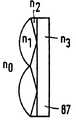
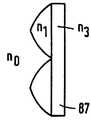
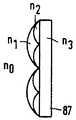
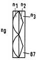
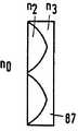
이러한 결합은 기판(87)위에서 서로 다른 굴절율(n1및 n2)을 가지는 층을 제공함으로써 형성될 수 있다. n0는 공기의 굴절율을 나타내고, n3는 기관의 굴절율을 나타낸다. 제4d도및 제4f도는 몇몇 실시예를 도시한다. 제4e도에서, 제공되는 층은 굴절율(n1)을 가지는 단지 하나의 재료를 사용하기에 충분한 형상을 가진다Such a bond can be formed by providing layers with different refractive indices n1 and n2 on the
다른 가능성은 예를 들면 이온교환에 의하여 기판(89)에서 굴절율 변화를 제공하는 것이다. 굴절율의 공간분포는 기판(87)에 도시된 렌즈형상의 영역에 의하여 표시된다. n0는 공기의 굴절율을 나타내고, n3는 이온교환이 없는 기판재료의 굴절율을 나타낸다. 이온 교환에 의하여, 굴절율(n1및 n2)을 가진 영역은 제4g도 및 제 4i도의 경우와, 제4h도의 경우에 단일 굴절율(n1)로 실현된다.Another possibility is to provide a refractive index change in the substrate 89, for example by ion exchange. The spatial distribution of the refractive index is represented by the lens-shaped region shown on the
몇몇 렌즈 구조는 상술된 방법중의 2개의 방법을 조합함으로써 제조될 수 있다.Some lens structures can be manufactured by combining two of the methods described above.
상기 렌즈 구조가 제4d도, 제4e도 및, 제4f도에 도시된 바와같은 구조이라면, 상기 렌즈 구조용 기관(87)은 예를 들면, 구조체가 LC 뭍질로 부터 이격된 기판쪽에 제공되는 LC 물질의 기판이 될 수 있다. 상기 방법에서, LC물질은 오염되지 않는다.If the lens structure is the structure as shown in FIGS. 4d, 4e and 4f, the
제1도에 도시된 바와같이, 본 발명에 따른 영상 표시 장치에서 영상 표시 패널(3)은 필드 롄즈(11, 13)에 의하여 앞서가고 연속으로 될 수 있으므로, 텔레센트릭 조명이 얻어진다. 이것의 장점은 마이크로 렌즈와 영상 표시 패널의 화소의 상대위치가 영상 표시 패널위의 위치에는 독립적이다. 상기 필드 렌즈(11, 13)은 임의적인 것이기 때문에, 이들은 파선으로 도시된다.As shown in Fig. 1, in the video display device according to the present invention, the
Claims (7)
Translated fromKoreanApplications Claiming Priority (3)
| Application Number | Priority Date | Filing Date | Title |
|---|---|---|---|
| EP95202961.9 | 1995-11-02 | ||
| EP95202961 | 1995-11-02 | ||
| PCT/IB1996/001144WO1997016765A1 (en) | 1995-11-02 | 1996-10-24 | Picture display device |
Publications (2)
| Publication Number | Publication Date |
|---|---|
| KR987001098A KR987001098A (en) | 1998-04-30 |
| KR100258292B1true KR100258292B1 (en) | 2000-06-01 |
Family
ID=8220789
Family Applications (1)
| Application Number | Title | Priority Date | Filing Date |
|---|---|---|---|
| KR1019970704545AExpired - Fee RelatedKR100258292B1 (en) | 1995-11-02 | 1996-10-24 | Picture display device |
Country Status (6)
| Country | Link |
|---|---|
| US (1) | US5731857A (en) |
| EP (1) | EP0801765A1 (en) |
| JP (1) | JPH10512377A (en) |
| KR (1) | KR100258292B1 (en) |
| CN (1) | CN1133893C (en) |
| WO (1) | WO1997016765A1 (en) |
Families Citing this family (38)
| Publication number | Priority date | Publication date | Assignee | Title |
|---|---|---|---|---|
| JP3779052B2 (en)* | 1997-12-17 | 2006-05-24 | 株式会社半導体エネルギー研究所 | LCD projector |
| US6678023B1 (en) | 1997-12-17 | 2004-01-13 | Semiconductor Energy Laboratory Co., Ltd. | Liquid crystal projector |
| JP4103216B2 (en)* | 1998-12-09 | 2008-06-18 | ノーリツ鋼機株式会社 | Photo printing device |
| GB2354899A (en) | 1999-10-02 | 2001-04-04 | Sharp Kk | Optical device for projection display |
| US6835535B2 (en) | 2000-07-31 | 2004-12-28 | Corning Incorporated | Microlens arrays having high focusing efficiency |
| US7092165B2 (en)* | 2000-07-31 | 2006-08-15 | Corning Incorporated | Microlens arrays having high focusing efficiency |
| EP1305656A4 (en) | 2000-07-31 | 2006-03-08 | Rochester Photonics Corp | Structure screens for controlled spreading of light |
| WO2004019120A1 (en)* | 2002-08-21 | 2004-03-04 | Nokia Corporation | Switchable lens display |
| TWI289708B (en) | 2002-12-25 | 2007-11-11 | Qualcomm Mems Technologies Inc | Optical interference type color display |
| US7301587B2 (en) | 2003-02-28 | 2007-11-27 | Nec Corporation | Image display device and portable terminal device using the same |
| JP4255334B2 (en)* | 2003-08-20 | 2009-04-15 | シャープ株式会社 | Display device |
| US7342705B2 (en)* | 2004-02-03 | 2008-03-11 | Idc, Llc | Spatial light modulator with integrated optical compensation structure |
| US20060066586A1 (en)* | 2004-09-27 | 2006-03-30 | Gally Brian J | Touchscreens for displays |
| US7807488B2 (en)* | 2004-09-27 | 2010-10-05 | Qualcomm Mems Technologies, Inc. | Display element having filter material diffused in a substrate of the display element |
| US7355780B2 (en)* | 2004-09-27 | 2008-04-08 | Idc, Llc | System and method of illuminating interferometric modulators using backlighting |
| US7750886B2 (en)* | 2004-09-27 | 2010-07-06 | Qualcomm Mems Technologies, Inc. | Methods and devices for lighting displays |
| US7561323B2 (en)* | 2004-09-27 | 2009-07-14 | Idc, Llc | Optical films for directing light towards active areas of displays |
| JP4722539B2 (en)* | 2005-04-27 | 2011-07-13 | 株式会社 日立ディスプレイズ | Display device |
| US20070097291A1 (en)* | 2005-10-31 | 2007-05-03 | Hewlett-Packard Development Company, Lp | Polymer dispersed liquid crystal |
| US7876400B2 (en) | 2005-10-31 | 2011-01-25 | Hewlett-Packard Development Company, L.P. | Optical modulation system |
| US7612859B2 (en) | 2005-10-31 | 2009-11-03 | Hewlett-Packard Development Company, L.P. | Ultra-violet radiation absorbing grid |
| US7603001B2 (en)* | 2006-02-17 | 2009-10-13 | Qualcomm Mems Technologies, Inc. | Method and apparatus for providing back-lighting in an interferometric modulator display device |
| EP1943551A2 (en) | 2006-10-06 | 2008-07-16 | Qualcomm Mems Technologies, Inc. | Light guide |
| EP1943555B1 (en) | 2006-10-06 | 2012-05-02 | QUALCOMM MEMS Technologies, Inc. | Optical loss structure integrated in an illumination apparatus of a display |
| US8068710B2 (en) | 2007-12-07 | 2011-11-29 | Qualcomm Mems Technologies, Inc. | Decoupled holographic film and diffuser |
| US7949213B2 (en)* | 2007-12-07 | 2011-05-24 | Qualcomm Mems Technologies, Inc. | Light illumination of displays with front light guide and coupling elements |
| US20090168459A1 (en)* | 2007-12-27 | 2009-07-02 | Qualcomm Incorporated | Light guide including conjugate film |
| WO2009129264A1 (en)* | 2008-04-15 | 2009-10-22 | Qualcomm Mems Technologies, Inc. | Light with bi-directional propagation |
| GB2461907A (en)* | 2008-07-17 | 2010-01-20 | Sharp Kk | Angularly restricted display |
| US20100195310A1 (en)* | 2009-02-04 | 2010-08-05 | Qualcomm Mems Technologies, Inc. | Shaped frontlight reflector for use with display |
| US8172417B2 (en)* | 2009-03-06 | 2012-05-08 | Qualcomm Mems Technologies, Inc. | Shaped frontlight reflector for use with display |
| CN102449512A (en) | 2009-05-29 | 2012-05-09 | 高通Mems科技公司 | Illumination devices and methods of fabrication thereof |
| WO2010141388A1 (en)* | 2009-06-01 | 2010-12-09 | Qualcomm Mems Technologies, Inc. | Front light based optical touch screen |
| US8848294B2 (en) | 2010-05-20 | 2014-09-30 | Qualcomm Mems Technologies, Inc. | Method and structure capable of changing color saturation |
| CN104007556B (en)* | 2014-06-06 | 2017-02-15 | 南开大学 | Low crosstalk integrated imaging three-dimensional display method based on microlens array group |
| CN108461045B (en) | 2018-03-13 | 2020-06-19 | 京东方科技集团股份有限公司 | Display device and method of manufacturing the same |
| WO2023156826A1 (en)* | 2022-02-18 | 2023-08-24 | Zhang Chuanrui | 2d transparent display device |
| CN114967214B (en)* | 2022-05-30 | 2023-10-27 | 京东方科技集团股份有限公司 | Display device and control method of display device |
Citations (1)
| Publication number | Priority date | Publication date | Assignee | Title |
|---|---|---|---|---|
| JPH03267918A (en)* | 1990-02-01 | 1991-11-28 | Sharp Corp | Transmission type display device |
Family Cites Families (6)
| Publication number | Priority date | Publication date | Assignee | Title |
|---|---|---|---|---|
| US5187599A (en)* | 1990-02-01 | 1993-02-16 | Sharp Kabushiki Kaisha | Display including two microlens arrays with unequal focal lengths and congruent focal points |
| JP2884458B2 (en)* | 1992-05-11 | 1999-04-19 | キヤノン株式会社 | Liquid crystal display panel manufacturing method |
| JPH05346578A (en)* | 1992-06-15 | 1993-12-27 | Nippon Sheet Glass Co Ltd | Liquid crystal display panel |
| US5428468A (en)* | 1993-11-05 | 1995-06-27 | Alliedsignal Inc. | Illumination system employing an array of microprisms |
| US5396350A (en)* | 1993-11-05 | 1995-03-07 | Alliedsignal Inc. | Backlighting apparatus employing an array of microprisms |
| US5398125A (en)* | 1993-11-10 | 1995-03-14 | Minnesota Mining And Manufacturing Company | Liquid crystal projection panel having microlens arrays, on each side of the liquid crystal, with a focus beyond the liquid crystal |
- 1996
- 1996-10-24JPJP9517186Apatent/JPH10512377A/ennot_activeAbandoned
- 1996-10-24EPEP96933576Apatent/EP0801765A1/ennot_activeWithdrawn
- 1996-10-24WOPCT/IB1996/001144patent/WO1997016765A1/ennot_activeApplication Discontinuation
- 1996-10-24KRKR1019970704545Apatent/KR100258292B1/ennot_activeExpired - Fee Related
- 1996-10-24CNCNB961920394Apatent/CN1133893C/ennot_activeExpired - Fee Related
- 1996-10-31USUS08/742,075patent/US5731857A/ennot_activeExpired - Fee Related
Patent Citations (1)
| Publication number | Priority date | Publication date | Assignee | Title |
|---|---|---|---|---|
| JPH03267918A (en)* | 1990-02-01 | 1991-11-28 | Sharp Corp | Transmission type display device |
Also Published As
| Publication number | Publication date |
|---|---|
| EP0801765A1 (en) | 1997-10-22 |
| CN1176008A (en) | 1998-03-11 |
| CN1133893C (en) | 2004-01-07 |
| JPH10512377A (en) | 1998-11-24 |
| US5731857A (en) | 1998-03-24 |
| WO1997016765A1 (en) | 1997-05-09 |
| KR987001098A (en) | 1998-04-30 |
Similar Documents
| Publication | Publication Date | Title |
|---|---|---|
| KR100258292B1 (en) | Picture display device | |
| US6286961B1 (en) | Illuminating optical system and projection type display | |
| KR100381827B1 (en) | Color LCD Projection Display System | |
| JP7624741B2 (en) | Small projector for head mounted display | |
| KR100400114B1 (en) | Video projection device with high efficiency lighting devices and such devices | |
| JP3409587B2 (en) | Optical path conversion optical element, image display device, and light projector | |
| US5161042A (en) | Color liquid crystal display device using dichroic mirrors for focusing different colors in different directions | |
| JP3298437B2 (en) | Optical element, polarized illumination device and projection display device | |
| EP0717910B1 (en) | Colour liquid crystal projection display systems | |
| JPH08211334A (en) | Light sources, 3D displays and directional displays | |
| KR20050042053A (en) | Three-dimensional display method and device therefor | |
| EP0467447B1 (en) | Image projection apparatus | |
| US5909316A (en) | Single plate projection type color liquid crystal display device | |
| CN1071457C (en) | Optical projection system with a novel lens system | |
| KR100635594B1 (en) | Projection type display devices and lighting optical systems for them | |
| JPS62226778A (en) | Rear projector | |
| JPH10170860A (en) | Eyeball projection type video display device | |
| JPH11502040A (en) | Image display device having two microlens arrays | |
| EP1052856A2 (en) | Reflection type color projector | |
| KR100811575B1 (en) | Liquid crystal display element and projection type liquid crystal display device | |
| JP3746905B2 (en) | Image projector | |
| KR100254335B1 (en) | LCD Display | |
| CN219302828U (en) | Backlight assembly, display device and vehicle | |
| EP0409620B1 (en) | A projection type color image display device | |
| KR0136061B1 (en) | Over head setting optical display apparatus |
Legal Events
| Date | Code | Title | Description |
|---|---|---|---|
| PA0105 | International application | St.27 status event code:A-0-1-A10-A15-nap-PA0105 | |
| R17-X000 | Change to representative recorded | St.27 status event code:A-3-3-R10-R17-oth-X000 | |
| A201 | Request for examination | ||
| PA0201 | Request for examination | St.27 status event code:A-1-2-D10-D11-exm-PA0201 | |
| PG1501 | Laying open of application | St.27 status event code:A-1-1-Q10-Q12-nap-PG1501 | |
| R18-X000 | Changes to party contact information recorded | St.27 status event code:A-3-3-R10-R18-oth-X000 | |
| R18-X000 | Changes to party contact information recorded | St.27 status event code:A-3-3-R10-R18-oth-X000 | |
| R17-X000 | Change to representative recorded | St.27 status event code:A-3-3-R10-R17-oth-X000 | |
| PN2301 | Change of applicant | St.27 status event code:A-3-3-R10-R13-asn-PN2301 St.27 status event code:A-3-3-R10-R11-asn-PN2301 | |
| E902 | Notification of reason for refusal | ||
| PE0902 | Notice of grounds for rejection | St.27 status event code:A-1-2-D10-D21-exm-PE0902 | |
| P11-X000 | Amendment of application requested | St.27 status event code:A-2-2-P10-P11-nap-X000 | |
| P13-X000 | Application amended | St.27 status event code:A-2-2-P10-P13-nap-X000 | |
| E701 | Decision to grant or registration of patent right | ||
| PE0701 | Decision of registration | St.27 status event code:A-1-2-D10-D22-exm-PE0701 | |
| PN2301 | Change of applicant | St.27 status event code:A-3-3-R10-R13-asn-PN2301 St.27 status event code:A-3-3-R10-R11-asn-PN2301 | |
| GRNT | Written decision to grant | ||
| PR0701 | Registration of establishment | St.27 status event code:A-2-4-F10-F11-exm-PR0701 | |
| PR1002 | Payment of registration fee | St.27 status event code:A-2-2-U10-U12-oth-PR1002 Fee payment year number:1 | |
| PG1601 | Publication of registration | St.27 status event code:A-4-4-Q10-Q13-nap-PG1601 | |
| FPAY | Annual fee payment | Payment date:20030306 Year of fee payment:4 | |
| PR1001 | Payment of annual fee | St.27 status event code:A-4-4-U10-U11-oth-PR1001 Fee payment year number:4 | |
| LAPS | Lapse due to unpaid annual fee | ||
| PC1903 | Unpaid annual fee | St.27 status event code:A-4-4-U10-U13-oth-PC1903 Not in force date:20040310 Payment event data comment text:Termination Category : DEFAULT_OF_REGISTRATION_FEE | |
| PC1903 | Unpaid annual fee | St.27 status event code:N-4-6-H10-H13-oth-PC1903 Ip right cessation event data comment text:Termination Category : DEFAULT_OF_REGISTRATION_FEE Not in force date:20040310 | |
| R18-X000 | Changes to party contact information recorded | St.27 status event code:A-5-5-R10-R18-oth-X000 | |
| PN2301 | Change of applicant | St.27 status event code:A-5-5-R10-R13-asn-PN2301 St.27 status event code:A-5-5-R10-R11-asn-PN2301 | |
| R18-X000 | Changes to party contact information recorded | St.27 status event code:A-5-5-R10-R18-oth-X000 | |
| R18-X000 | Changes to party contact information recorded | St.27 status event code:A-5-5-R10-R18-oth-X000 | |
| R18-X000 | Changes to party contact information recorded | St.27 status event code:A-5-5-R10-R18-oth-X000 |