KR100255514B1 - Fabricating method of semiconductor memory device - Google Patents
Fabricating method of semiconductor memory deviceDownload PDFInfo
- Publication number
- KR100255514B1 KR100255514B1KR1019970050198AKR19970050198AKR100255514B1KR 100255514 B1KR100255514 B1KR 100255514B1KR 1019970050198 AKR1019970050198 AKR 1019970050198AKR 19970050198 AKR19970050198 AKR 19970050198AKR 100255514 B1KR100255514 B1KR 100255514B1
- Authority
- KR
- South Korea
- Prior art keywords
- film
- insulating film
- ion implantation
- oxide film
- peripheral circuit
- Prior art date
- Legal status (The legal status is an assumption and is not a legal conclusion. Google has not performed a legal analysis and makes no representation as to the accuracy of the status listed.)
- Expired - Fee Related
Links
Images


Classifications
- H—ELECTRICITY
- H10—SEMICONDUCTOR DEVICES; ELECTRIC SOLID-STATE DEVICES NOT OTHERWISE PROVIDED FOR
- H10B—ELECTRONIC MEMORY DEVICES
- H10B12/00—Dynamic random access memory [DRAM] devices
- H10B12/30—DRAM devices comprising one-transistor - one-capacitor [1T-1C] memory cells
- H10B12/48—Data lines or contacts therefor
- H10B12/485—Bit line contacts
- H—ELECTRICITY
- H01—ELECTRIC ELEMENTS
- H01L—SEMICONDUCTOR DEVICES NOT COVERED BY CLASS H10
- H01L21/00—Processes or apparatus adapted for the manufacture or treatment of semiconductor or solid state devices or of parts thereof
- H01L21/70—Manufacture or treatment of devices consisting of a plurality of solid state components formed in or on a common substrate or of parts thereof; Manufacture of integrated circuit devices or of parts thereof
- H01L21/71—Manufacture of specific parts of devices defined in group H01L21/70
- H01L21/768—Applying interconnections to be used for carrying current between separate components within a device comprising conductors and dielectrics
- H01L21/76897—Formation of self-aligned vias or contact plugs, i.e. involving a lithographically uncritical step
- H—ELECTRICITY
- H10—SEMICONDUCTOR DEVICES; ELECTRIC SOLID-STATE DEVICES NOT OTHERWISE PROVIDED FOR
- H10B—ELECTRONIC MEMORY DEVICES
- H10B12/00—Dynamic random access memory [DRAM] devices
- H10B12/01—Manufacture or treatment
- H10B12/09—Manufacture or treatment with simultaneous manufacture of the peripheral circuit region and memory cells
- H—ELECTRICITY
- H10—SEMICONDUCTOR DEVICES; ELECTRIC SOLID-STATE DEVICES NOT OTHERWISE PROVIDED FOR
- H10D—INORGANIC ELECTRIC SEMICONDUCTOR DEVICES
- H10D84/00—Integrated devices formed in or on semiconductor substrates that comprise only semiconducting layers, e.g. on Si wafers or on GaAs-on-Si wafers
- H10D84/01—Manufacture or treatment
- H10D84/0123—Integrating together multiple components covered by H10D12/00 or H10D30/00, e.g. integrating multiple IGBTs
- H10D84/0126—Integrating together multiple components covered by H10D12/00 or H10D30/00, e.g. integrating multiple IGBTs the components including insulated gates, e.g. IGFETs
- H10D84/0149—Manufacturing their interconnections or electrodes, e.g. source or drain electrodes
Landscapes
- Engineering & Computer Science (AREA)
- Manufacturing & Machinery (AREA)
- Physics & Mathematics (AREA)
- Condensed Matter Physics & Semiconductors (AREA)
- General Physics & Mathematics (AREA)
- Computer Hardware Design (AREA)
- Microelectronics & Electronic Packaging (AREA)
- Power Engineering (AREA)
- Semiconductor Memories (AREA)
- Internal Circuitry In Semiconductor Integrated Circuit Devices (AREA)
Abstract
Description
Translated fromKorean본 발명은 반도체 제조 분야에 관한 것으로, 특히 동일 웨이퍼 상에 셀 영역과 주변 회로 영역을 형성하는 반도체 메모리 장치의 제조에 관한 것이다.TECHNICAL FIELD The present invention relates to the field of semiconductor manufacturing, and more particularly, to the manufacture of semiconductor memory devices forming cell regions and peripheral circuit regions on the same wafer.
일반적으로, 반도체 장치의 고집적화 추세에 따라 반도체 장치 제조시의 공정 여유도를 확보하는 것이 중요한 해결 과제가 되고 있다.In general, securing a process margin in manufacturing a semiconductor device has become an important problem in accordance with a trend toward higher integration of semiconductor devices.
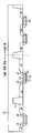
첨부된 도면 도 1a 내지 도 1c는 본 발명이 해당하는 종래기술을 설명하기 위한 것으로, 이하 이를 통해 종래의 DRAM 제조 기술 및 그 문제점을 살펴본다.1A to 1C illustrate the prior art to which the present invention pertains. Hereinafter, the conventional DRAM manufacturing technology and its problems will be described.
먼저, 도 1a에 도시된 바와 같이 준비된 웨이퍼(10)의 소정 부분에 소자 분리막(11)을 형성하고, 게이트 산화막(12) 및 게이트 전극(13)을 형성한다. 계속하여, 셀 영역과 주변 회로 영역에 N-이온주입 및 P-이온주입을 실시하고, 게이트 전극(13) 측벽 부분에 스페이서 산화막(14)을 형성한 다음, 주변 회로 영역에 N+이온주입 및 P+이온주입을 실시하여 LDD(lightly doped drain) 구조의 모스 트랜지스터를 형성한다. 도면에서 N+, N-, P+, P-는 각각 소오스/드레인을 구성하는 불순물 도핑 영역, 19는 게이트 마스크 산화막을 각각 나타낸 것이다.First, an
다음으로, 도 1b에 도시된 바와 같이 전체 구조 상부에 층간 절연막(15)을 증착하고, 이를 선택적 식각하여 비트 라인 콘택홀을 형성한다.Next, as shown in FIG. 1B, an
계속하여, 도 1c에 도시된 바와 같이 콘택홀 스페이서(16)를 형성하고, 전체 구조 상부에 폴리실리콘막(17) 및 실리사이드막(18)을 형성한 다음, 이를 패터닝하여 비트 라인을 형성한다.Subsequently, as shown in FIG. 1C, a
이후, 후속 공정을 진행한다.Thereafter, the subsequent process is performed.
상기와 같이 진행되는 종래의 DRAM 제조 기술에서 스페이서 산화막은 셀 영역과 주변 회로 영역에서 동시에 형성되는데, 이러한 스페이서 산화막은 특히 주변 회로 소자의 전기적 특성에 매우 큰 영향을 미치게 된다. 주변 회로 지역에서 소자의 전기적 특성을 확보하기 위한 스페이서 산화막의 최적화된 두께는 800Å 내지 1500Å 정도이다.In the conventional DRAM fabrication technology proceeding as described above, the spacer oxide film is formed at the same time in the cell region and the peripheral circuit region. Such a spacer oxide film has a great influence on the electrical characteristics of the peripheral circuit element. The optimized thickness of the spacer oxide film for securing the electrical characteristics of the device in the peripheral circuit area is about 800 kW to 1500 kW.
그러나, 반도체 메모리 장치의 고집적화에 따라 셀 영역에서 게이트 전극간의 간격이 좁아지게 되고, 이에 따라 비트 라인 콘택의 면적이 감소하여 비트 라인의 접촉 저항이 증가하는 문제점이 있기 때문에 스페이서 산화막을 충분한 두께로 형성할 수 없었다.However, due to the high integration of the semiconductor memory device, the gap between the gate electrodes in the cell region is narrowed, and accordingly, the area of the bit line contact decreases, thereby increasing the contact resistance of the bit line. I could not.
또한, 이러한 문제점을 고려하여 스페이서 산화막을 얇게 형성할 경우, 비트 라인 콘택을 형성할 때 정렬 오차를 감안하면 정상적인 스페이서 산화막 형성 공정을 사용하는데 많은 어려움이 있을 수 있고, 경우에 따라서는 비트 라인 콘택 형성 공정 자체가 불가능하게 된다. 또한 비트 라인 콘택 형성이 이루어졌다 하더라도 상기한 바와 같은 주변 회로 영역의 최적화된 두께를 충족시킬 수 없게 되어 반도체 메모리 장치의 전기적 특성을 열화 시키는 문제점이 발생하게 된다.In addition, when the spacer oxide film is thinly formed in view of such a problem, it may be difficult to use a normal spacer oxide film formation process in view of alignment errors when forming the bit line contact, and in some cases, the bit line contact formation The process itself becomes impossible. In addition, even if the bit line contact is formed, the optimized thickness of the peripheral circuit region as described above may not be satisfied, resulting in a problem of deteriorating electrical characteristics of the semiconductor memory device.
본 발명은 셀 영역의 비트 라인 콘택 공정 여유도를 확보하는 동시에 주변 회로 영역의 최적화된 두께의 스페이서 절연막을 제공하는 반도체 메모리 장치 제조방법을 제공하는데 그 목적이 있다.SUMMARY OF THE INVENTION An object of the present invention is to provide a method of manufacturing a semiconductor memory device which provides a spacer insulating film having an optimized thickness of a peripheral circuit region while securing a margin of a bit line contact process in a cell region.
도 1a 내지 도 1c는 종래기술에 따른 DRAM 제조 공정도.1A-1C show a DRAM manufacturing process according to the prior art.
도 2a 내지 도 2c는 본 발명의 일실시예에 따른 DRAM 제조 공정도.2A-2C illustrate a DRAM manufacturing process in accordance with one embodiment of the present invention.
* 도면의 주요 부분에 대한 부호의 설명* Explanation of symbols for the main parts of the drawings
20 : 웨이퍼 21 : 소자 분리막20
22 : 게이트 산화막 23 : 게이트 전극22
24 : 질화막 25 : 산화막24
26 : 포토레지스트 패턴 27 : 층간 절연막26
28 : 폴리실리콘막 29 : 실리사이드막28
30 : 게이트 마스크 산화막30: gate mask oxide film
상기와 같은 목적을 달성하기 위하여 본 발명의 반도체 메모리 장치 제조방법은 반도체 웨이퍼 상에 소자 분리막, 게이트 산화막 및 게이트 전극을 형성하는 단계; 저농도 소오스/드레인 이온주입을 실시하는 단계; 전체 구조 상부에 제1 절연막 및 상기 제1 절연막과 식각 선택비를 갖는 제2 절연막을 차례로 증착하는 단계; 주변 회로 영역의 상기 제2 절연막 및 상기 제1 절연막을 차례로 비등방성 식각하여 상기 게이트 전극 측벽 부분에 스페이서 절연막을 형성하는 단계; 고농도 소오스/드레인 이온주입을 실시하는 단계; 전체 구조 상부에 층간 절연막을 형성하는 단계; 및 셀 영역의 상기 층간 절연막 및 상기 제2 및 제1 절연막을 선택적 식각하여 비트 라인 콘택홀을 형성하되, 상기 제1 절연막의 스페이서 패턴이 형성되어 자기 정렬 콘택홀이 형성되도록 하는 단계를 포함하여 이루어진다.In order to achieve the above object, the semiconductor memory device manufacturing method of the present invention comprises the steps of forming a device isolation film, a gate oxide film and a gate electrode on a semiconductor wafer; Performing low concentration source / drain ion implantation; Sequentially depositing a first insulating film and a second insulating film having an etch selectivity with the first insulating film on the entire structure; Anisotropically etching the second insulating film and the first insulating film in a peripheral circuit region to form a spacer insulating film on the sidewall portion of the gate electrode; Performing a high concentration source / drain ion implantation; Forming an interlayer insulating film over the entire structure; And selectively etching the interlayer insulating layer and the second and first insulating layers of the cell region to form a bit line contact hole, wherein a spacer pattern of the first insulating layer is formed to form a self-aligning contact hole. .
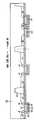
이하, 첨부된 도면 도 2a 내지 도 2c를 참조하여 본 발명의 일실시예를 상술한다.Hereinafter, an embodiment of the present invention will be described in detail with reference to the accompanying drawings, FIGS. 2A to 2C.
우선, 도 2a에 도시된 바와 같이 준비된 웨이퍼(20)의 소정 부분에 소자 분리막(21)을 형성하고, 게이트 산화막(22) 및 게이트 전극(23)을 형성한다. 계속하여, 셀 영역과 주변 회로 영역에 N-이온주입 및 P-이온주입을 실시하고, 전체 구조 상부에 질화막(24) 및 산화막(25)을 차례로 증착한다. 여기서, 질화막(24)의 두께는 셀 영역에서 게이트 전극간의 간격과 비트 라인 접촉 저항 및 자기 정렬 공정에 필요한 최소의 두께로 결정되며, 질화산화막으로 대체하여 사용할 수 있다. 또한, 산화막(25)은 주변 회로 소자의 전기적 특성을 고려하여 임의로 조정할 수 있다. 도면에서 N-, P-는 각각 소오스/드레인을 구성하는 불순물 도핑 영역, 30은 게이트 마스크 산화막을 각각 나타낸 것이다.First, an
다음으로, 도 2b에 도시된 바와 같이 셀 영역 상부에 포토레지스트 패턴(26)을 형성하고, 이를 식각 장벽으로 하여 주변 회로 영역의 산화막(25) 및 질화막(24)을 차례로 비등방성 식각하여 게이트 전극(23) 측벽 부분에 이중 구조의 스페이서 절연막을 형성한 다음, 주변 회로 영역에 N+이온주입 및 P+이온주입을 실시하여 LDD(lightly doped drain) 구조의 모스 트랜지스터를 형성한다. 도면에서 N+, P+는 각각 소오스/드레인을 구성하는 불순물 도핑 영역을 나타낸 것이다.Next, as shown in FIG. 2B, the
다음으로, 도 2c에 도시된 바와 같이 포토레지스트 패턴(26)을 제거하고, 전체 구조 상부에 층간 절연막(27)을 증착한 후, 이를 선택적 식각하여 비트 라인 콘택홀을 형성한다. 이때, 셀 영역에서는 층간 절연막(27) 및 산화막(25), 그리고 질화막(24)이 선택적으로 식각되어 질화막(24)의 스페이서 패턴이 형성되고, 자기 정렬 콘택홀이 형성된다. 계속하여, 전체 구조 상부에 폴리실리콘막(28) 및 실리사이드막(29)을 증착하고, 이를 패터닝하여 비트 라인을 형성한다. 여기서, 장벽금속막은 필요에 따라 사용한다.Next, as shown in FIG. 2C, the
상기한 일실시예에 나타난 바와 같이 본 발명은 종래 웨이퍼 전반에 걸쳐 동일한 두께로 형성되는 스페이서 절연막을 질화막/산화막 또는 질화산화막/산화막(즉, 서로 큰 식각 선택비를 갖는 두 절연막)의 이중층을 사용하여 형성함으로서, 셀 영역에서는 얇게 형성하여 비트 라인 콘택 저항을 낮추고 주변 회로 영역에서는 충분한 두께로 최적화할 수 있다. 또한, 자기 정렬 콘택을 이루어 비트 라인 콘택 공정의 공정 마진을 확보할 수 있다.As shown in the above embodiment, the present invention uses a double layer of a nitride film / oxide film or a nitride oxide film / oxide film (that is, two insulating films each having a large etching selectivity) as a spacer insulating film formed with the same thickness throughout the conventional wafer. By forming a thin film in the cell region, the bit line contact resistance can be lowered and a sufficient thickness can be optimized in the peripheral circuit region. In addition, a self alignment contact may be made to secure a process margin of the bit line contact process.
이상에서 설명한 본 발명은 전술한 실시예 및 첨부된 도면에 의해 한정되는 것이 아니고, 본 발명의 기술적 사상을 벗어나지 않는 범위 내에서 여러 가지 치환, 변형 및 변경이 가능하다는 것이 본 발명이 속하는 기술분야에서 통상의 지식을 가진 자에게 있어 명백할 것이다.The present invention described above is not limited to the above-described embodiments and the accompanying drawings, and various substitutions, modifications, and changes can be made in the art without departing from the technical spirit of the present invention. It will be apparent to those of ordinary knowledge.
상기한 바와 같이 본 발명은 셀 영역과 주변 회로 영역의 스페이서 절연막을 각각 다른 두께로 최적화함으로서 반도체 메모리 장치의 전기적 특성을 향상시키는 효과가 있으며, 이와 더불어 셀 지역의 비트 라인 콘택 공정의 여유도를 개선하는 효과가 있다.As described above, the present invention has the effect of improving the electrical characteristics of the semiconductor memory device by optimizing the spacer insulating films of the cell region and the peripheral circuit region to different thicknesses, and also improving the margin of the bit line contact process in the cell region. It is effective.
Claims (4)
Translated fromKoreanPriority Applications (1)
| Application Number | Priority Date | Filing Date | Title |
|---|---|---|---|
| KR1019970050198AKR100255514B1 (en) | 1997-09-30 | 1997-09-30 | Fabricating method of semiconductor memory device |
Applications Claiming Priority (1)
| Application Number | Priority Date | Filing Date | Title |
|---|---|---|---|
| KR1019970050198AKR100255514B1 (en) | 1997-09-30 | 1997-09-30 | Fabricating method of semiconductor memory device |
Publications (2)
| Publication Number | Publication Date |
|---|---|
| KR19990027705A KR19990027705A (en) | 1999-04-15 |
| KR100255514B1true KR100255514B1 (en) | 2000-05-01 |
Family
ID=19522001
Family Applications (1)
| Application Number | Title | Priority Date | Filing Date |
|---|---|---|---|
| KR1019970050198AExpired - Fee RelatedKR100255514B1 (en) | 1997-09-30 | 1997-09-30 | Fabricating method of semiconductor memory device |
Country Status (1)
| Country | Link |
|---|---|
| KR (1) | KR100255514B1 (en) |
Cited By (1)
| Publication number | Priority date | Publication date | Assignee | Title |
|---|---|---|---|---|
| KR100542844B1 (en)* | 2001-10-11 | 2006-01-20 | 가부시끼가이샤 도시바 | Semiconductor device and manufacturing method thereof |
Families Citing this family (1)
| Publication number | Priority date | Publication date | Assignee | Title |
|---|---|---|---|---|
| KR100318320B1 (en)* | 1999-05-10 | 2001-12-22 | 김영환 | Method for fabricating semiconductor device |
- 1997
- 1997-09-30KRKR1019970050198Apatent/KR100255514B1/ennot_activeExpired - Fee Related
Cited By (1)
| Publication number | Priority date | Publication date | Assignee | Title |
|---|---|---|---|---|
| KR100542844B1 (en)* | 2001-10-11 | 2006-01-20 | 가부시끼가이샤 도시바 | Semiconductor device and manufacturing method thereof |
Also Published As
| Publication number | Publication date |
|---|---|
| KR19990027705A (en) | 1999-04-15 |
Similar Documents
| Publication | Publication Date | Title |
|---|---|---|
| KR100317532B1 (en) | Semiconductor device and method for fabricating the same | |
| KR100287009B1 (en) | Process for fabricating semiconductor device having polycide line and impurity region respectively exposed to contact holes different in depth | |
| JP2585140B2 (en) | Wiring contact structure of semiconductor device | |
| KR100487951B1 (en) | A semiconductor device having self-aligned contact hole and fabrication method thereof | |
| JP2780162B2 (en) | Method for manufacturing semiconductor device | |
| KR19990088569A (en) | Semiconductor device in which hot carrier resistance can be improved and silicide layer can be formed with high reliability and method of manufacturing it | |
| KR100308515B1 (en) | Method of manufacturing semiconductor device | |
| KR100255514B1 (en) | Fabricating method of semiconductor memory device | |
| KR20010004237A (en) | A method for forming semiconductor memory device including self-aligned contact process | |
| KR20000020583A (en) | Method for manufacturing semiconductor device | |
| KR100321758B1 (en) | Manufacturing method of semiconductor device | |
| KR100243738B1 (en) | Method for manufacturing semiconductor device | |
| KR20020096393A (en) | Method for Fabricating MOS transistor | |
| KR100198637B1 (en) | Method of manufacturing semiconductor device | |
| KR100390891B1 (en) | Manufacturing method of highly integrated semiconductor device | |
| KR100356472B1 (en) | Method of manufacturing a semiconductor device | |
| KR0146245B1 (en) | Capacitor Manufacturing Method of Semiconductor Device | |
| KR100399926B1 (en) | Method of manufacturing a transistor in a semiconductor device | |
| KR0123745B1 (en) | Contact formation method of semiconductor device | |
| KR100321759B1 (en) | Method for fabricating semiconductor device | |
| KR100362195B1 (en) | A method for fabricating SRAM | |
| KR19980025851A (en) | Manufacturing method of highly integrated semiconductor device for forming fine contact | |
| KR970011758B1 (en) | A method for fabricating dram cells | |
| KR19980068069A (en) | Manufacturing Method of Semiconductor Device | |
| KR20040056195A (en) | Method for forming of mos transistor |
Legal Events
| Date | Code | Title | Description |
|---|---|---|---|
| A201 | Request for examination | ||
| PA0109 | Patent application | St.27 status event code:A-0-1-A10-A12-nap-PA0109 | |
| PA0201 | Request for examination | St.27 status event code:A-1-2-D10-D11-exm-PA0201 | |
| R17-X000 | Change to representative recorded | St.27 status event code:A-3-3-R10-R17-oth-X000 | |
| PG1501 | Laying open of application | St.27 status event code:A-1-1-Q10-Q12-nap-PG1501 | |
| E701 | Decision to grant or registration of patent right | ||
| PE0701 | Decision of registration | St.27 status event code:A-1-2-D10-D22-exm-PE0701 | |
| GRNT | Written decision to grant | ||
| PR0701 | Registration of establishment | St.27 status event code:A-2-4-F10-F11-exm-PR0701 | |
| PR1002 | Payment of registration fee | St.27 status event code:A-2-2-U10-U11-oth-PR1002 Fee payment year number:1 | |
| PG1601 | Publication of registration | St.27 status event code:A-4-4-Q10-Q13-nap-PG1601 | |
| PN2301 | Change of applicant | St.27 status event code:A-5-5-R10-R13-asn-PN2301 St.27 status event code:A-5-5-R10-R11-asn-PN2301 | |
| PN2301 | Change of applicant | St.27 status event code:A-5-5-R10-R13-asn-PN2301 St.27 status event code:A-5-5-R10-R11-asn-PN2301 | |
| R17-X000 | Change to representative recorded | St.27 status event code:A-5-5-R10-R17-oth-X000 | |
| PR1001 | Payment of annual fee | St.27 status event code:A-4-4-U10-U11-oth-PR1001 Fee payment year number:4 | |
| PR1001 | Payment of annual fee | St.27 status event code:A-4-4-U10-U11-oth-PR1001 Fee payment year number:5 | |
| PR1001 | Payment of annual fee | St.27 status event code:A-4-4-U10-U11-oth-PR1001 Fee payment year number:6 | |
| PR1001 | Payment of annual fee | St.27 status event code:A-4-4-U10-U11-oth-PR1001 Fee payment year number:7 | |
| PR1001 | Payment of annual fee | St.27 status event code:A-4-4-U10-U11-oth-PR1001 Fee payment year number:8 | |
| FPAY | Annual fee payment | Payment date:20080102 Year of fee payment:9 | |
| PR1001 | Payment of annual fee | St.27 status event code:A-4-4-U10-U11-oth-PR1001 Fee payment year number:9 | |
| LAPS | Lapse due to unpaid annual fee | ||
| PC1903 | Unpaid annual fee | St.27 status event code:A-4-4-U10-U13-oth-PC1903 Not in force date:20090216 Payment event data comment text:Termination Category : DEFAULT_OF_REGISTRATION_FEE | |
| PC1903 | Unpaid annual fee | St.27 status event code:N-4-6-H10-H13-oth-PC1903 Ip right cessation event data comment text:Termination Category : DEFAULT_OF_REGISTRATION_FEE Not in force date:20090216 | |
| PN2301 | Change of applicant | St.27 status event code:A-5-5-R10-R13-asn-PN2301 St.27 status event code:A-5-5-R10-R11-asn-PN2301 | |
| PN2301 | Change of applicant | St.27 status event code:A-5-5-R10-R13-asn-PN2301 St.27 status event code:A-5-5-R10-R11-asn-PN2301 | |
| PN2301 | Change of applicant | St.27 status event code:A-5-5-R10-R13-asn-PN2301 St.27 status event code:A-5-5-R10-R11-asn-PN2301 | |
| P22-X000 | Classification modified | St.27 status event code:A-4-4-P10-P22-nap-X000 | |
| P22-X000 | Classification modified | St.27 status event code:A-4-4-P10-P22-nap-X000 | |
| P22-X000 | Classification modified | St.27 status event code:A-4-4-P10-P22-nap-X000 | |
| P22-X000 | Classification modified | St.27 status event code:A-4-4-P10-P22-nap-X000 |