KR100251689B1 - Active matrix display - Google Patents
Active matrix displayDownload PDFInfo
- Publication number
- KR100251689B1 KR100251689B1KR1019970016924AKR19970016924AKR100251689B1KR 100251689 B1KR100251689 B1KR 100251689B1KR 1019970016924 AKR1019970016924 AKR 1019970016924AKR 19970016924 AKR19970016924 AKR 19970016924AKR 100251689 B1KR100251689 B1KR 100251689B1
- Authority
- KR
- South Korea
- Prior art keywords
- active matrix
- matrix display
- display
- amplifier
- output
- Prior art date
- Legal status (The legal status is an assumption and is not a legal conclusion. Google has not performed a legal analysis and makes no representation as to the accuracy of the status listed.)
- Expired - Fee Related
Links
Images


Classifications
- G—PHYSICS
- G02—OPTICS
- G02F—OPTICAL DEVICES OR ARRANGEMENTS FOR THE CONTROL OF LIGHT BY MODIFICATION OF THE OPTICAL PROPERTIES OF THE MEDIA OF THE ELEMENTS INVOLVED THEREIN; NON-LINEAR OPTICS; FREQUENCY-CHANGING OF LIGHT; OPTICAL LOGIC ELEMENTS; OPTICAL ANALOGUE/DIGITAL CONVERTERS
- G02F1/00—Devices or arrangements for the control of the intensity, colour, phase, polarisation or direction of light arriving from an independent light source, e.g. switching, gating or modulating; Non-linear optics
- G02F1/01—Devices or arrangements for the control of the intensity, colour, phase, polarisation or direction of light arriving from an independent light source, e.g. switching, gating or modulating; Non-linear optics for the control of the intensity, phase, polarisation or colour
- G02F1/13—Devices or arrangements for the control of the intensity, colour, phase, polarisation or direction of light arriving from an independent light source, e.g. switching, gating or modulating; Non-linear optics for the control of the intensity, phase, polarisation or colour based on liquid crystals, e.g. single liquid crystal display cells
- G02F1/133—Constructional arrangements; Operation of liquid crystal cells; Circuit arrangements
- G02F1/136—Liquid crystal cells structurally associated with a semi-conducting layer or substrate, e.g. cells forming part of an integrated circuit
- G02F1/1362—Active matrix addressed cells
- G02F1/13624—Active matrix addressed cells having more than one switching element per pixel
- G—PHYSICS
- G09—EDUCATION; CRYPTOGRAPHY; DISPLAY; ADVERTISING; SEALS
- G09G—ARRANGEMENTS OR CIRCUITS FOR CONTROL OF INDICATING DEVICES USING STATIC MEANS TO PRESENT VARIABLE INFORMATION
- G09G3/00—Control arrangements or circuits, of interest only in connection with visual indicators other than cathode-ray tubes
- G09G3/20—Control arrangements or circuits, of interest only in connection with visual indicators other than cathode-ray tubes for presentation of an assembly of a number of characters, e.g. a page, by composing the assembly by combination of individual elements arranged in a matrix no fixed position being assigned to or needed to be assigned to the individual characters or partial characters
- G09G3/22—Control arrangements or circuits, of interest only in connection with visual indicators other than cathode-ray tubes for presentation of an assembly of a number of characters, e.g. a page, by composing the assembly by combination of individual elements arranged in a matrix no fixed position being assigned to or needed to be assigned to the individual characters or partial characters using controlled light sources
- G—PHYSICS
- G09—EDUCATION; CRYPTOGRAPHY; DISPLAY; ADVERTISING; SEALS
- G09G—ARRANGEMENTS OR CIRCUITS FOR CONTROL OF INDICATING DEVICES USING STATIC MEANS TO PRESENT VARIABLE INFORMATION
- G09G3/00—Control arrangements or circuits, of interest only in connection with visual indicators other than cathode-ray tubes
- G09G3/20—Control arrangements or circuits, of interest only in connection with visual indicators other than cathode-ray tubes for presentation of an assembly of a number of characters, e.g. a page, by composing the assembly by combination of individual elements arranged in a matrix no fixed position being assigned to or needed to be assigned to the individual characters or partial characters
- G09G3/34—Control arrangements or circuits, of interest only in connection with visual indicators other than cathode-ray tubes for presentation of an assembly of a number of characters, e.g. a page, by composing the assembly by combination of individual elements arranged in a matrix no fixed position being assigned to or needed to be assigned to the individual characters or partial characters by control of light from an independent source
- G09G3/36—Control arrangements or circuits, of interest only in connection with visual indicators other than cathode-ray tubes for presentation of an assembly of a number of characters, e.g. a page, by composing the assembly by combination of individual elements arranged in a matrix no fixed position being assigned to or needed to be assigned to the individual characters or partial characters by control of light from an independent source using liquid crystals
- G09G3/3611—Control of matrices with row and column drivers
- G09G3/3648—Control of matrices with row and column drivers using an active matrix
- G—PHYSICS
- G02—OPTICS
- G02F—OPTICAL DEVICES OR ARRANGEMENTS FOR THE CONTROL OF LIGHT BY MODIFICATION OF THE OPTICAL PROPERTIES OF THE MEDIA OF THE ELEMENTS INVOLVED THEREIN; NON-LINEAR OPTICS; FREQUENCY-CHANGING OF LIGHT; OPTICAL LOGIC ELEMENTS; OPTICAL ANALOGUE/DIGITAL CONVERTERS
- G02F2202/00—Materials and properties
- G02F2202/10—Materials and properties semiconductor
- G02F2202/104—Materials and properties semiconductor poly-Si
- G—PHYSICS
- G09—EDUCATION; CRYPTOGRAPHY; DISPLAY; ADVERTISING; SEALS
- G09G—ARRANGEMENTS OR CIRCUITS FOR CONTROL OF INDICATING DEVICES USING STATIC MEANS TO PRESENT VARIABLE INFORMATION
- G09G2300/00—Aspects of the constitution of display devices
- G09G2300/08—Active matrix structure, i.e. with use of active elements, inclusive of non-linear two terminal elements, in the pixels together with light emitting or modulating elements
- G09G2300/0809—Several active elements per pixel in active matrix panels
- G09G2300/0833—Several active elements per pixel in active matrix panels forming a linear amplifier or follower
- G—PHYSICS
- G09—EDUCATION; CRYPTOGRAPHY; DISPLAY; ADVERTISING; SEALS
- G09G—ARRANGEMENTS OR CIRCUITS FOR CONTROL OF INDICATING DEVICES USING STATIC MEANS TO PRESENT VARIABLE INFORMATION
- G09G2300/00—Aspects of the constitution of display devices
- G09G2300/08—Active matrix structure, i.e. with use of active elements, inclusive of non-linear two terminal elements, in the pixels together with light emitting or modulating elements
- G09G2300/0809—Several active elements per pixel in active matrix panels
- G09G2300/0842—Several active elements per pixel in active matrix panels forming a memory circuit, e.g. a dynamic memory with one capacitor
- G—PHYSICS
- G09—EDUCATION; CRYPTOGRAPHY; DISPLAY; ADVERTISING; SEALS
- G09G—ARRANGEMENTS OR CIRCUITS FOR CONTROL OF INDICATING DEVICES USING STATIC MEANS TO PRESENT VARIABLE INFORMATION
- G09G2320/00—Control of display operating conditions
- G09G2320/02—Improving the quality of display appearance
- G09G2320/0209—Crosstalk reduction, i.e. to reduce direct or indirect influences of signals directed to a certain pixel of the displayed image on other pixels of said image, inclusive of influences affecting pixels in different frames or fields or sub-images which constitute a same image, e.g. left and right images of a stereoscopic display
- G09G2320/0214—Crosstalk reduction, i.e. to reduce direct or indirect influences of signals directed to a certain pixel of the displayed image on other pixels of said image, inclusive of influences affecting pixels in different frames or fields or sub-images which constitute a same image, e.g. left and right images of a stereoscopic display with crosstalk due to leakage current of pixel switch in active matrix panels
- G—PHYSICS
- G09—EDUCATION; CRYPTOGRAPHY; DISPLAY; ADVERTISING; SEALS
- G09G—ARRANGEMENTS OR CIRCUITS FOR CONTROL OF INDICATING DEVICES USING STATIC MEANS TO PRESENT VARIABLE INFORMATION
- G09G2320/00—Control of display operating conditions
- G09G2320/02—Improving the quality of display appearance
- G09G2320/0247—Flicker reduction other than flicker reduction circuits used for single beam cathode-ray tubes
Landscapes
- Physics & Mathematics (AREA)
- Engineering & Computer Science (AREA)
- General Physics & Mathematics (AREA)
- Nonlinear Science (AREA)
- Chemical & Material Sciences (AREA)
- Crystallography & Structural Chemistry (AREA)
- Computer Hardware Design (AREA)
- Theoretical Computer Science (AREA)
- Mathematical Physics (AREA)
- Optics & Photonics (AREA)
- Microelectronics & Electronic Packaging (AREA)
- Liquid Crystal Display Device Control (AREA)
- Liquid Crystal (AREA)
- Control Of Indicators Other Than Cathode Ray Tubes (AREA)
Abstract
Translated fromKoreanDescription
Translated fromKorean종래 알려져 있는 액티브매트릭스 디스플레이는 액정등의 표시재료의 광학특성을 제어하도록, 매트릭스상으로 배치된 어드레스배선내에 액티브회로를 갖는다. 제1도는 전형적인 액티브매트릭스 디스플레이의 구성을 나타낸다. 참조부호 (1)은 화소(화소)가 규칙적으로 배치된 단(短)형상의 어레이에 배치된다. 화소어레이(1)의 행의 어드레스는 스캔드라이버(2)에 의해 행해지고, 열의 어드레스는 데이터드라이버(3)에 의해 행해진다. 참조부호(4)는 전형적인 화소의 회로를 나타낸다.The known active matrix display has an active circuit in the address wiring arranged in a matrix so as to control the optical characteristics of display materials such as liquid crystal. 1 shows the configuration of a typical active matrix display.
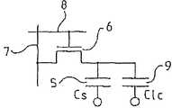
각 화소는 홀드커패시터(5)에 병렬로 접속된 표시소자(도시안됨)을 가진다. 홀드커패시터(5)는 박막전계효과트랜지스터(6)의 소스와, 콘몬배선 또는 하나전의 게이트배선 사이에 접속된다. 트랜지스터(6)의 게이트는 그의 화소가 속하는 행의 전 화소에 공통의 스캔전극(8)에 접속된다. 또한, 트랜지스터(6)의 드레인은 그의 화소가 속하는 전 화소에 공통의 데이터전극(7)에 접속된다. 각 스캔전극(8)은 스캔드라이버(2)의 출력중의 대응하는 것에 접속되며, 각 데이터전극(7)은 데이터드라이버(3)의 출력중 대응하는 것에 접속된다.Each pixel has a display element (not shown) connected in parallel to the
동작시에는, 각 행의 화소 표시데이타는, 스캔드라이버(2)에서 스캔전극(8)에 주기적으로 반복하여 공급되는 스캔펄스에 동기하여, 데이터드라이버(3)에서 데이터전극(7)으로 공급된다. 이 때문에, 동일행의 화소는 전 행이 리프레쉬되어 1프레임의 표시데이타의 리프레쉬가 완료될때까지 동시에 리프레쉬된다. 그후, 다음 프레임의 데이터에 대해 상기 프로세스가 반복된다.In operation, the pixel display data of each row is supplied from the
각 화소의 스캔전극(8)이 스캔드라이버(2)에서 스캔펄스를 받게되면, 데이터 전극(7)의 전압에 의해 홀드커패시터(5)가 충전된다. 스캔펄스가 제거되면, 트랜지스터(6)는 홀드커패시터(5)를 데이터전극(7)에서 분리시킨다. 이에 따라 관련된 표시소자의 광학특성은, 그의 화소가 다음 프레임에서 리프레쉬될때까지 홀드커패시터(5)에 인가된 전압에 대응하게 된다.When the
액티브매트릭스 액정 디스플레이에서는 홀드 커패시터(5)에 축적된 전압이 액정층의 광학특성을 변조하도록 이용된다. 종래 알려져 있는 디스플레이에서는, 스위칭소자로서 이용되는 트랜지스터(6)가 아모르퍼스실리콘 박막 트랜지스터로 구성된다. 각 화소의 리프레쉬 사이클의 사이에서, 커패시터(5)에 축적된 전압의 동적인 흔들림은 화질을 결정하는 면에서 상당히 중요하다.In an active matrix liquid crystal display, the voltage accumulated in the
액정장치에서는, 인가전압과 액정상의 표면저하 사이의 관계는 비선형적이고, 시간의존성을 갖는다. 이는 유전율이방성으로 알려져 있다. 이것은 액정장치의 실효용량이 인가전압과 액정의 응답속도의 관계로 됨을 암시하는 것이다. 종래의 액티브매트릭스 액정장치의 화소에서는 비이상적인 액정용량(C1c)(제2도에 9로 나타냄)이 고정된 축적용량(Cs)에 병렬로 접속되어 있다. 스캔펄스를 스캔전극(8)에 공급함에 의해 화소에 어드레스되면, 그 화소의 트랜지스터(6)의 게이트전압은 비교적 짧은 시간동안 하이로 되며, 이에따라 표시소자는 눈에 보이는 플리커를 방지하기에 충분한 속도로 리프레쉬된다. 따라서, 병렬로 접속된 커패시터(5)와 표시소자(9)의 조합을 갖는 용량의 충전시간은 액정용량(C1c)의 전압의존성이 실질적으로 어떠한 여향도 미치지 않을 만틈 충분히 짧다. 이 때문에 액정용량(C1c)은 스캔펄스가 단속되는 사이에 일정하게 될 수 있다. 그러므로, 스캔펄스와 스캔펄스 사이에서는, 트랜지스터(6)가 커패시터(5) 및 표시소자(9)를 실질적으로 분리시키게 됨으로써, 병렬로 접속된 커패시터(5) 및 표시소자(9) 전체의 전하는 실질적으로 일정하게 된다. 액정이 인가전압에 응답하면, 액정용량(C1c)이 변화되기 때문에, 표시소자에 걸리는 최종적인 전압은 펄스의 진폭과 동일하게 되고, 화소의 스캔중에 데이터전극(7)에 공급되는 데이터전압에는 대응하지 않게 된다. 액정이 정의 유전율이방성을 갖는 경우에는, 용량이 증대되어 액정표시소자에 걸리는 전압이 저하한다.In the liquid crystal device, the relationship between the applied voltage and the surface drop of the liquid crystal phase is nonlinear and has time dependency. This is known as dielectric anisotropy. This implies that the effective capacitance of the liquid crystal device is a relationship between the applied voltage and the response speed of the liquid crystal. In the pixels of the conventional active matrix liquid crystal device, the non-ideal liquid crystal capacitor C1c (shown as 9 in FIG. 2) is connected in parallel to the fixed storage capacitor Cs. When a scan pulse is addressed to a pixel by supplying it to the
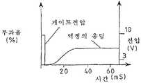
제3a도-제3c도는 유전율이방성의 영향을 나타낸 그래프이고, 각각 시간에 대한 게이트전압 및 디스플레이의 투과율을 나타낸다. 제3a도는 1 리프레쉬 기간에 하나의 펄스를 공급할 때의 액정의 응답을 나타낸다. 데이터전극의 전압은 게이트전압을 비교적 단속기간이 짧은 펄스의 형태로 제공한다. 이 도면에서는 실현된 투과율의 값을 좌측의 종축상에 나타내지만, 실제의 액정표시소자의 투과특성은 실현된 투과율보다도 낮게 된다. 즉, 액정이 전압에 응답하면, 용량이 증대하여 액정에 걸리는 전압이 저하되는 결과로 투과율이 소망하는 값에 도달하지 않는다.3A to 3C are graphs showing the influence of dielectric anisotropy, and show the gate voltage and the transmittance of the display with respect to time, respectively. 3A shows the response of the liquid crystal when one pulse is supplied in one refresh period. The voltage of the data electrode provides the gate voltage in the form of a pulse having a relatively short intermittent period. Although the figure of the realized transmittance is shown on the vertical axis on the left side in this figure, the transmission characteristic of the actual liquid crystal display element is lower than the realized transmittance. That is, when the liquid crystal responds to the voltage, the transmittance does not reach the desired value as a result of the increase in capacitance and the drop in the voltage applied to the liquid crystal.
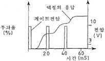
제3b도는 제3a도에 대응하는 그래프로서, 복수의 리프레쉬 기간(도면에서는 3회의 리프레쉬 기간)에서 화소에 동일한 데이터신호를 공급할때의 영향을 나타낸다. 이와같이, 일련의 스캔펄스를 화소에 공급함으로써 소망하는 투과율을 실현시킬 수 있다.FIG. 3B is a graph corresponding to FIG. 3A, which shows the effect of supplying the same data signal to the pixels in a plurality of refresh periods (three refresh periods in the figure). In this way, the desired transmittance can be realized by supplying a series of scan pulses to the pixel.
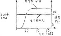
제3c도는 제3a도 및 제3b도에 대응하는 것으로, 보다 낮은 임피던스의 전원에서의 액정용량의 충전의 영향을 나타낸다. 이는, 예컨대 트랜지스터(6)를 보다 긴 기간에 걸쳐 온상태로 하여, 그에따라 홀드커패시터(5) 및 액정용량(C1c)을 비교적 낮은 출력 임피던스를 갖는 데이터드라이버(3)의 각 출력으로부터 충전함에 의해 실현된다. 따라서, 액정표시소자는 원하는 투과율을 실현할 수 있지만, 디스플레이를 리프레쉬할 수 있는 비율은 대폭 감소하며, 플리커 등의 바람직하지 않는 현상이 관찰되게 된다.FIG. 3C corresponds to FIGS. 3A and 3B and shows the effect of charging of the liquid crystal capacitance in a lower impedance power supply. This is achieved by, for example, turning on the
비이상적인 용량의 영향을 감소시키는 방법으로서, 홀드 커패시터의 용량 (Cs)을 비이상적인 액정용량(C1c)보다 상당히 크게 하는 방법이 알려져 있다. 이 방법은 전형적으로 10-4C/㎡의 표면전하밀도를 갖는 전형적인 네마틱재료에 대해 사용될 수 있다. 따라서, 스위치된 상태에 의해 표면전하밀도가 크게 다른 액정 모드로 된다. 이러한 재료를 종래의 액티브매트릭스 구동방법을 이용하여 구동하면, 스캔전극이 하이로 되는 기간중에 높은 값의 전하를 공급할 필요가 있다. 스캔 기간 사이에는, 액정재료가 응답하기에 충분한 시간이 없기 때문에, 상당히 큰 축적 커패시터, 상당히 높은 데이터전압과 종래 사이즈의 커패시터, 또는 이러한 큰 축적 커패시터, 상당히 높은 데이터전압과 종래 사이즈의 커패시터, 또는 이러한 방법들을 조합한 방법이 필요하게 된다. 일반적으로, 이러한 조건에서 종래의 액티브 매트릭스 구동방법을 이용하는 것을 검토하면, 실용적이지 않다. 즉, 큰 용량 및/또는 전압을 조합하면, 개구율 또는 디스플레이의 소비전력에 악영향이 미치게 된다. 이러한 재료로는, 예컨대 표면안정화 강유전액정과 같은 자발분극을 갖는 액정장치, 또는 일렉트로클리닉스(electroclinics), 헬리오일렉트릭(helioeleectrics), 변형된 헬릭스 강유전, 반강유전, 랜덤상 및 칼럼너등의 전계유도 자발분극을 갖는 액정장치가 포함된다.As a method of reducing the influence of the non-ideal capacitance, a method is known in which the capacitance Cs of the hold capacitor is considerably larger than the non-ideal liquid crystal capacitance C1c. This method can be used for typical nematic materials, which typically have a surface charge density of 10-4 C /
유전율이방성의 영향 외에도, 박막트랜지스터(6)의 리크전류의 영향도 시각적으로 바람직하지 않은 현상을 야기하는 요인중 하나이다. 리크전류는 게이트전압이 임계전압보다 낮을 때 트랜지스터의 채널을 흐르는 전류이다. 리크전류가 높으면, 액정표시소자에 걸리는 전압이 프레임 기간의 사이에 대폭 저하된다. 그 결과, 표시소자의 투과특성이, 리프레쉬와 리프레쉬 사이에 현저하게 변화되어, 디스플레이를 관찰하는 관찰자에게 플리커가 관찰되게 된다.In addition to the influence of dielectric anisotropy, the influence of the leakage current of the
근래의 박막 트랜지스터 제조기술의 전진에 의해, 고성능 폴리실리콘 박막트랜지스터의 개발이 진행되고 있다. 특히, 현재에는, 이러한 트랜지스터를 디스플레이에 이용되는 유리기판에 적합하게 낮은 온도에서 제조할 수 있게 되었다. 또한, 이러한 트랜지스터는 종래의 아모르퍼스 실리콘 박막트랜지스터에 비해 구동능력도 향상되고, 디스플레이의 각 화소내만이 아니라, 드라이버(2, 3)등의 고속의 주변구동회로에서 이용되고 있다. 이에 따라, 구동회로를 탑재한 디스플레이의 제조 비용을 감소시킬 수 있다.With the recent advancement of the thin film transistor manufacturing technology, the development of a high performance polysilicon thin film transistor is progressing. In particular, at present, such transistors can be manufactured at low temperatures suitable for glass substrates used in displays. In addition, such a transistor has improved driving capability compared with conventional amorphous silicon thin film transistors, and is used not only in each pixel of the display but also in high-speed peripheral driving circuits such as
화소 레벨에서는, 폴리실리콘 트랜지스터는 아모르퍼스실리콘 트랜지스터보다 작게될 수 있어서, 이에따라 개구율을 높이고, 스캔전압의 피드스루 (feedthrough)를 감소시킬 수 있다. 따라서, 폴리실리콘 박막 트랜지스터의 리크전류는 아모르퍼스 실리콘 박막 트랜지스터보다 상당히 크고, 트랜지스터(6)의 게이트-소스간의 전압과 드레인-소스간의 전압에 상당히 의존하는 오프상태에서의 리크는 디스플레이패널내에서 가장 변화가 심한 변수중 하나로 된다. 따라서, 이러한 특징은 액티브매트릭스 액정디스플레이 패널에 스위칭소자로서 폴리실리콘 박막트랜지스터를 이용하는 경우의 주요 문제로 된다.At the pixel level, the polysilicon transistor can be made smaller than the amorphous silicon transistor, thereby increasing the aperture ratio and reducing the feedthrough of the scan voltage. Therefore, the leakage current of the polysilicon thin film transistor is considerably larger than that of the amorphous silicon thin film transistor, and the leakage in the off state, which is highly dependent on the voltage between the gate-source and the drain-source voltage of the
제4도는 2종류의 상이한 온도 및 2종류의 드레인-소스 전압에서, 게이트-소스 전압에 대한 드레인 전류를 나타내며, 드레인 전류는 로그를 이용하여 나타낸다. 드레인-소스 전압을 낮추면, 어느온도에서도 리크전류는 지수적으로 감소한다. 이 때문에, 알려져 있는 바와같이, 트랜지스터의 드레인에서의 전계를 작게함에 의해 리크전류를 감소시킬 수 있다. 이를 실현하기 위한 방법으로서, F. Okumura and K. Sera, A. M. L. C. D., p24-27(1994)에는, 저농도 도프 드레인(LDD)구조, 옵셋게이트(OG)구조, 액티브게이트(AG)구조 및 멀티게이트가 개시되어 있다.FIG. 4 shows the drain current with respect to the gate-source voltage at two different temperatures and two kinds of drain-source voltages, and the drain current is shown using a logarithm. By lowering the drain-source voltage, the leakage current decreases exponentially at any temperature. For this reason, as is known, the leakage current can be reduced by making the electric field at the drain of the transistor small. As a method for realizing this, in F. Okumura and K. Sera, AMLCD, p24-27 (1994), a low concentration doped drain (LDD) structure, an offset gate (OG) structure, an active gate (AG) structure, and a multigate are provided. Is disclosed.
LDD 구조 및 OG구조는, 드레인에서의 전계를 감소시키고, 온전류에 악영향을 미치며, 결과적으로 트랜지스터의 속도를 감소시킨다. 따라서, 이러한 구조는 일체형 디스플레이에는 이상적이지 않다. 일체형 딧플레이에서는, 오프전류의 감소가 중요하게 되는 화소트랜지스터와, 고속화가 중요하게 되는 구동회로용트랜지스터를 다른 프로세스에서 제조할 필요가 있다. 이와 같이 여분의 공정이 발생되는 것은 바람직하지 않으며, 또한 제조 비용도 상당히 증가시킨다.The LDD structure and the OG structure reduce the electric field at the drain, adversely affect the on current, and consequently reduce the speed of the transistor. Thus, this structure is not ideal for integrated displays. In an integrated dipplay, it is necessary to manufacture pixel transistors in which off current reduction is important and drive circuit transistors in which high speed is important in other processes. It is not desirable for this extra process to occur and also significantly increases the manufacturing cost.
멀티게이트 구조를 채용하는 경우에는, 제5도에 도시된 바와같이, 직렬로 접속된 2이상의 박막 트랜지스터를 이용하고 있다. 제5도에 도시된 구성에서는, 제1도 및 제2도에 도시된 구성에서의 단일의 게이트를 갖는 트랜지스터(6)가 트랜지스터(6a, 6b)에 등가로 된 멀티플게이트 트랜지스터로 치환되었다. 그러나, 상기 구성에서는, 여분의 리크전류를 방지하도록 충분히 전계를 감소시킬 수 없게 되므로, 이 중종 구조는 LDD구조와 함께 사용된다.In the case of employing the multi-gate structure, as shown in FIG. 5, two or more thin film transistors connected in series are used. In the configuration shown in Fig. 5, the
그외 알려져 있는 방법을 제6도에 나타낸다. 이 방법에서는, 멀티게이트구조의 접합부(실제로는 트랜지스터(6a, 6b 사이)에 홀드커패시터(10)를 부가하고 있다. 그러나, 이러한 구성에 의해, 바람직하지 않은 시각적인 현상을 발생시키지 않는 폴리실리콘 박막 트랜지스터를 디스플레이에 이용할 수 있는 가능성이 충분하게 홀드시간을 제공할 것이지 의심스럽게 된다.Other known methods are shown in FIG. In this method, the
제7도는 일본국 특허공개공보 93-142573호에 개시된, 홀드시간을 어려 프레임에 대해 연장시키는 방법을 적용시킨 회로를 나타낸다. 이 회로는 유니티게인을 갖는 앰프(11)의 입력을 커패시터(5) 및 표시소자(9)에 접속하고, 출력을 트랜지스터(6a, 6b) 사이의 접합부에 접속함에 의해피드백기능을 가진다. 이에 따라, 커패시터(5) 및 표시소자(9)에 인가되는 전압은 직렬로 접속된 박막트랜지스터(6a, 6b)의 접합부에 나타난다. 버퍼앰프(11)가 이상적으로 되고, 커패시터(5) 및 표시소자 (9)의 용량에서 전하가 배출되지 않으면, 액정에서의 리크가 없게된다.FIG. 7 shows a circuit to which the hold time is extended to a young frame disclosed in Japanese Patent Laid-Open No. 93-142573. This circuit has a feedback function by connecting the input of the
유럽 특허 제 0 586 155호는 제8도에 도시된 액티브매트릭스 액정디스플레이를 개시하고 있다. 이 액티브매트릭스 액정 디스플레이는 제1도에 도시된 것과 거의 동일한 구성을 갖지만, 유니티게인을 갖는 버퍼앰프(11)가 각 화소의 디스플레이 회로에 설치되어 있는 점에서 제1도에 도시된 디스플레이와 다르다. 앰프(11)의 입력은 트랜지스터(6)의 소스와 홀드커패시터(5)에 접속되며, 출력은 액정표시소자 (9)에 접속된다. 상기 앰프(11)는 상당히 높은 입력 임피던스와 비교적 낮은 출력 임피던스를 갖는다.
스캔전극(8)에 스캔펄스를 공급함에 의해 화소를 어드레스하면, 트랜지스터 (6)는 온상태로 절환되고, 홀드커패시터(5)는 데이터전극(7)에 인가되는 전압까지 충전된다. 전극(8)에 인가되는 스캔펄스와 스캔펄스 사이에서는, 트랜지스터(6)가 오프상태로 절환된다. 앰프(11)의 출력은 커패시터(5)애 인가되는 전압에 따르게 되며, 표시소자(9)에 그 전압을 공급한다.When the pixel is addressed by supplying a scan pulse to the
앰프(11)의 출력임피던스가 비교적 낮으면, 표시소자(9)는 전압구동된다. 따라서, 표시소자(9)에 인가되는 전압은 실질적으로 일정하게 유지된다. 이 때문에, 프레임리프레쉬 기간 전체에서 액정에 인가되는 전압이 스텝상으로 된다.If the output impedance of the
유럽 특허 제 0 586 155호는 연속되는 리프레쉬 사이에 표시소자에 인가되는 전압의 저하를 유발하는 표시소자(9)의 전극간의 리크전류의 영향을 없애는 것에 관련된 것이지만, 액정의 유전율이방성의 영향도 또한 실질적으로 감소시키거나, 또는 제거하게 된다.
제8도에 나타낸 유럽 특허 제 0 586 155호에 개시된 회로에서는, 앰프(11)를 이용하여, 표시소자(9)에 걸리는 전압을 홀드커패시터(5)에 걸리는 전압과 강제로 동일하게 함에 의해, 액정의 유전율이 변화하여도 표시소자(9)의 전압이 변화하지 않게된다. 그러나, 이 회로에서는 홀드커패시터(5)에 축적된 전하가 트랜지스터(6)를 통해 배출될 수 있기 때문에, 커패시터(5)에 걸리는 전압이 저하하게 되며, 그 결과 표시소자(9)에 걸리는 전압도 저하하게 된다. 또한, 유럽 특허 제 0 586 155호에 개시된 회로에서는 트랜지스터(6)의 오프시의 리크전류에 기인하는 표시전압의 저하를 방지할 수 없다.In the circuit disclosed in
본 발명은 이러한 현상을 감안한 것으로, 액정의 유전율이방성이 표시에 미치는 영향을 실질적으로 없애고, 각 화소의 게이트에서 리크전류가 표시에 미치는 영향도 실질적으로 제거할 수 있는 액티브매트릭스 디스플레이를 제공하는 것을 목적으로 한다.SUMMARY OF THE INVENTION The present invention has been made in view of this phenomenon, and an object of the present invention is to provide an active matrix display which can substantially eliminate the influence of the dielectric anisotropy of the liquid crystal on the display and substantially eliminate the influence of the leakage current on the display at the gate of each pixel. It is done.
본 발명에 의하면, 데이터 전극에 접속되는 데이터 입력, 및 스캔전극에 접속되는 스캔입력을 갖는 게이트를 각각 포함하는 복수의 화소, 게이트의 출력에 접속되는 홀드커패시터, 홀드커패시터에 접속되는 입력을 갖는 버퍼앰프, 및 버퍼앰프의 출력에 접속되는 표시소자를 포함하는 액티브매트릭스 디스플레이를 제공한다. 상기 게이트느 직렬로 접속된 제1 및 제2 반도체스위츠를 가지며, 상기 버퍼 앰프의 출력은 상기 제1 및 제2 반도체스위치 사이의 노드에 접속된다.According to the present invention, a buffer having a plurality of pixels each including a gate having a data input connected to the data electrode and a scan input connected to the scan electrode, a hold capacitor connected to the output of the gate, and an input connected to the hold capacitor An active matrix display comprising an amplifier and a display element connected to the output of a buffer amplifier is provided. The gate has first and second semiconductor switches connected in series, and the output of the buffer amplifier is connected to a node between the first and second semiconductor switches.
이에 의해, 반도체장치의 리크전류의 바람직하지 않은 영향 액정의 유전율이방성의 영향이 실질적으로 감소되거나, 또는 제거되는 디스플레이를 제공할 수 있게 된다. 이 디스를레이에서는 리프레쉬 속도를 상승시킬수 있고 플리커등의 시각적으로 바람직하지 않은 현상을 감소시킬 수 있다. 다른 방법을 이용하는 표시소자에 대해서, 홀드 커패시터는, 그렇지 않은 경우에 표시소자에 의해 야기되는 바람직하지 않은 영향으로부터 실질적으로 분리된다. 반도체장치는 화소용 디스플레이에 일체로 탑재되는 구동회로용과 동일한 프로세스 공정을 이용하여 제조된다. 이에 따라, 실질적으로 제조 비용을 증가시키지 않는다.This makes it possible to provide a display in which the influence of the dielectric constant anisotropy of the liquid crystal is substantially reduced or eliminated. This display can increase the refresh rate and reduce visually undesirable phenomena such as flicker. For display elements using other methods, the hold capacitor is substantially separated from the undesirable effects caused by the display elements. The semiconductor device is manufactured using the same process steps as for the driving circuit which is integrally mounted on the pixel display. Thus, it does not substantially increase the manufacturing cost.
표시소자는 각각 액정표시소자로 될 수 있다.Each display element may be a liquid crystal display element.
앰프는 폴리실리콘 액티부소자를 구비할 수 있다. 액티브소자는 폴리실리콘 박막 트랜지스터를 구비할 수 있다.The amplifier may include a polysilicon actuating element. The active device may include a polysilicon thin film transistor.
바람직하게는, 앰프는 유니티게인을 갖는 것이다.Preferably, the amplifier has unity gain.
제1 및 제2 스위치 각각은 트랜지스터를 구비할 수 있다.Each of the first and second switches may have a transistor.
앰프는 소스플로워를 구비할 수 있다. 소스플로워는 일정전류로 하기위한 부하를 가질 수 있다.The amplifier may have a source follower. The source follower may have a load for constant current.
앰프는 상기 홀드커패시터에 접속되는 비반전입력과, 상기 출력에 접속되는 반전입력을 가진 차동앰프로 될 수 있다. 차동앰프는 공토의 부하에 접속되는 제1 및 제2 트랜지스터를 구비할 수 있다. 공토의 부하는 정전류발생기일 수 있다. 앰프는 상기 제1 및 제2 트랜지스터의 드레인에 접속되는 전류미러로 구성될 수 있다.The amplifier may be a differential amplifier having a non-inverting input connected to the hold capacitor and an inverting input connected to the output. The differential amplifier may have first and second transistors connected to the load of the clay. The load of the clay may be a constant current generator. The amplifier may be configured as a current mirror connected to the drains of the first and second transistors.
화소는 복수의 행으로 배치되며, 이 경우에 각 행의 화소의 스캔입력은 공통의 스캔적극에 접속되며, 상기 각 행의 화소의 앰프는 상기 행에 인접한 행에 대응하는 스캔전극 사이에 접속되는 전원단자를 가진다. 인접한 행의 화소는 역의 도전형의 반도체장치를 구비할 수 있다.The pixels are arranged in a plurality of rows, in which case the scan inputs of the pixels of each row are connected to a common scan active, and the amplifiers of the pixels of each row are connected between the scan electrodes corresponding to the rows adjacent to the rows. It has a power terminal. The pixels in adjacent rows may be provided with a reverse conductivity type semiconductor device.
상기 버퍼 앰프의 출력은 표시소자에 직접 접속되는 것이 바람직하다.The output of the buffer amplifier is preferably connected directly to the display element.
상기 버퍼 앰프의 출력은 스캔 입력에 제공된 주사 펄스에 독립적으로 상기 표시소자에 접속되는 것이 바람직하다.The output of the buffer amplifier is preferably connected to the display element independently of the scan pulse provided to the scan input.
본 발명의 바람직한 실시형태에서는, 액티브버퍼가 액티브매트릭스 디스플레이의 각 화소에 설치된다. 이 액티브버퍼는 입력이 홀드커패시터에, 출력이 액정셀에 접속되도록, 홀드커패시터와 액정셀 사이에 설치된다. 도한, 피드백루프가 버퍼의 출력에서 2개의 직렬로 접속된 폴리실리콘 박막트랜시스터의 접속부에 접속된다. 상기 2개의 직렬로 접속된 폴리실리콘 박막트랜지스터는 데이터배선에서 홀드커패시터로의 패스게이트로서 작용한다. 홀드커패시터는 비교적 작은 용량이고, 각행을 스캔하는 기간중에 충전되며, 버퍼의 입력에 기준전압을 공급한다. 이어서 버퍼는 프레임 기간의 잔여기간 동안, 액정셀을 일정전압으로 구동한다. 이러한 배치를 채용하면, 상당히 긴 기간동안 전하가 버퍼에서 공급되어, 상당히 높은 표면전하밀도를 가진 재료를 구동하는 것이 가능하다. 따라서, 고전압 및/또는 대용량의 홀드커패시터를 이용할 필요가 없고, 소비전력 또는 개구율면에서 유리하다. 버퍼의 출력은 2개의 직렬로 접속된 트랜지스터 사이의 노드에 피드백되도록 접속되며, 따라서 노드의 전압을 버퍼의 출력전압에 실질적으로 동일하게 되도록 하고 있다. 버퍼는 홀드커패시터의 전압에 따라, 액정용량과 패스트랜지스터의 접합부를 동시에 구동한다. 이러한 상황하에서, 이상적인 버퍼를 이용하면, 액정용량에 가까운 축의 트랜지스터의 드레인-소스전압이 실질적으로 제로로되고, 그에 따라 리크 전류도 실질적으로 제거된다.In a preferred embodiment of the present invention, an active buffer is provided in each pixel of the active matrix display. The active buffer is provided between the hold capacitor and the liquid crystal cell so that the input is connected to the hold capacitor and the output is connected to the liquid crystal cell. Also, a feedback loop is connected at the output of the buffer to the connection of two serially connected polysilicon thin film transistors. The two series-connected polysilicon thin film transistors act as pass gates to hold capacitors in the data wiring. The hold capacitor is a relatively small capacitor, charged during the scan of each row, and supplies a reference voltage to the input of the buffer. The buffer then drives the liquid crystal cell at a constant voltage for the remainder of the frame period. With this arrangement, it is possible for the charge to be supplied from the buffer for a fairly long period of time, driving the material with a fairly high surface charge density. Therefore, there is no need to use a high voltage and / or large capacity hold capacitor, which is advantageous in terms of power consumption or aperture ratio. The output of the buffer is connected to be fed back to the node between the two series connected transistors, thus making the voltage of the node substantially equal to the output voltage of the buffer. The buffer simultaneously drives the junction of the liquid crystal capacitor and the fast transistor in accordance with the voltage of the hold capacitor. Under such a situation, with an ideal buffer, the drain-source voltage of the transistor on the axis close to the liquid crystal capacitance becomes substantially zero, thereby also eliminating the leakage current.
제1도는 종래의 액태브매트릭스 디스플레이의 구성을 개략적으로 나타낸 도면.1 is a view schematically showing the configuration of a conventional active matrix display.
제2도는 제1도의 액티브매트릭스 디스플레이의 액티브소자의 구성을 나타낸 도면.2 is a diagram showing the configuration of an active element of the active matrix display of FIG.
제3a도-제3c도는 다른 게이트 파형에 대해 액정의 유전율이방성의 영향을 나타낸 도면.3a to 3c show the influence of dielectric anisotropy of liquid crystals on different gate waveforms.
제4도는 전형적인 폴리실리콘 박막트랜지스터에 있어서, 바이어스 전압에 대한 리크전류를 나타낸 도면.4 is a diagram showing a leakage current against a bias voltage in a typical polysilicon thin film transistor.
제5도는 리크전류를 감소시키기 위한 공지의 방법을 적용한 액티브매트릭스 디스플레이의 주요부의 구성을 나타낸 도면.5 is a diagram showing the configuration of main parts of an active matrix display to which a known method for reducing leakage current is applied.
제6도는 리크전류를 감소시키기 위한 공지의 다른 방법을 적용한 액티브매트릭스 디스플레이의 주요부의 구성을 나타낸 도면.Fig. 6 is a diagram showing the configuration of main parts of an active matrix display to which another known method for reducing the leakage current is applied.
제7도는 리크전류를 감소시키기 위한 공지의 또 다른 방법을 적용한 액티브매트릭스 디스플레이의 주요부의 구성을 나타낸 도면.FIG. 7 is a diagram showing the configuration of main parts of an active matrix display to which another known method for reducing the leakage current is applied.
제8도는 종래의 다른 액티브매트릭스 디스플레이의 구성을 개략적으로 나타낸 도면.8 is a diagram schematically showing the configuration of another conventional active matrix display.
제9도는 본 발명의 일실시예의 액티브매트릭스 디스플레이의 구성을 개략적으로 나타낸 도면.9 is a diagram schematically showing a configuration of an active matrix display of an embodiment of the present invention.
제10도는 제8도의 디스플레이에 이용된 앰프의 구성을 나타낸 도면.FIG. 10 shows the structure of an amplifier used for the display of FIG. 8. FIG.
제11도는 제8도의 디스플레이에 이용된 앰프의 다른 구성을 나타낸 도면.FIG. 11 shows another configuration of the amplifier used for the display of FIG. 8. FIG.
제12도는 제8도의 디스플레이에 이용된 앰프의 또 다른 구성을 나타낸 도면.FIG. 12 shows yet another configuration of an amplifier used for the display of FIG. 8. FIG.
제13도는 다른 액티브회로에서 리크전류의 영향을 나타낸 도면, 및13 shows the influence of the leakage current in another active circuit, and
제14도는 본 발명의 액티브매트릭스 디스플레이에 있어서, 화소의 액티브회로에 전압을 공급하기 위해 스캔배선을 이용한 구성을 나타낸 도면이다.FIG. 14 is a diagram showing a configuration in which the scan wiring is used to supply a voltage to the active circuit of the pixel in the active matrix display of the present invention.
제9도에 도시된 액티브 매트릭스 액정 디스플레이는 제8도에 도시한 디스플레이와 거의 동일한 구성을 갖지만, 트랜지스터(6)가 직렬로 접속된 트랜지스터 (6a, 6b)로 대체된 점에서 다르다. 상기 트랜지스터(6a, 6b)는 예컨대 제5도 내지 제7도에 도시된 멀티게이트 트랜지스터로서 작용한다. 또한, 제9도의 디스플레이에서는 앰프(11)의 출력이 트랜지스터(6a)의 소스와 트랜지스터(6b)의 드레인 사이에 접속부에 접속된다.The active matrix liquid crystal display shown in FIG. 9 has substantially the same configuration as the display shown in FIG. 8, but differs in that the
트랜지스터(6a)의 소스와 앰프(11) 사이의 접속부는 데이터배선에서의 초기 충전의 경로로 된다. 화소를 포함한 배선의 스캔후, 앰프(11)의 출력 및 트랜지지스터(6b)의 드레인은 홀드커패시터(5)와 동일 전위로 된다. 이 때문에, 표시소자 (9)에 걸리는 전압은 앰프(9)에 의해 강제로 홀드커패시터(5)에 걸리는 전압과 동일하게 유지되며, 액정의 유전율이 변화하여도 표시소자(9)의 전압은 변화하지 않는다. 또한, 표시소자(9)애 가까운 측의 트랜지스터(6b)의 드레인측의 전위를 앰프(9)의 출력전위와 동일한 전위로 함에 의해, 트랜지스터(6b)의 소스-드레인 전압은 실질적으로 제로로 되어, 이에 따라 트랜지스터(6b)의 리크전류(i1)도 실질적으로 제로로 된다. 이 때문에, 종래 문제로 되는 스위칭 소자의 리크전류에 기인한 홀드 커패시터(5)의 전압저하를 방지할 수 있어서, 리크전류가 표시에 악영향을 미치는 일이 실질적으로 없게된다.The connection portion between the source of the
유니티게인을 갖는 버퍼앰프(11)를 실현하기 위한 여러 가지 구성이 고려되지만, 어떤 구성을 채용하는가는, 앰프의 면적, 효율 및 허용 오차등의 여러 가지 점토에 의해 결정된다.Various configurations for realizing the
제10도는 버퍼앰프(11)의 일 구성예를 나타내며, 이 예애서 앰프(11)는 소스 플로워형으로 나타나 있다. 소스플로워는 전압공급배선(Vdd, Vss) 사이에 직렬로 접속된 엔핸스먼트 트랜지스터(12, 13)를 갖는다. 트랜지스터(12)의 게이트는 커패시터(5)에 접속된 앰프의 입력을 구성하며, 트랜지스터(12)의 소스는 앰프의 출력을 구성한다. 트랜지스터(13)의 게이트는 바이어스전압(Vb)애 접속되고, 트랜지스터(12)을 일정전류로 하기 위한 부하를 구성한다.10 shows an example of the configuration of the
제10도에 도시된 소스플로워에는, 액정표시소자(9)의 용량(C1c)의 변화에 추종하도록 필요한 전류와 리크를 보상하는데 필요한 전류를 공급하는 것만이 요구된다. 이 때문에, 상기 소스플로워의 전류의 요건은 극도로 작게된다.The source follower shown in FIG. 10 is only required to supply the current necessary to compensate for the current and the leak necessary to follow the change in the capacitance C1c of the liquid crystal display element 9. For this reason, the requirement of the current of the source follower is extremely small.
제11도에 도시된 바와 같이, 소스플로워를 디플레션트랜지스터(12a, 13a)로 구성할 수 있다. 이 경우에는, 트랜지스터(13a)의 게이트가 소스에 접속되어 정전류 발생기를 구성한다. 이 때문에, 바이어스 전압(Vb)은 필요없고, 여분의 전압 공급 배선을 생략할 수 있다.As shown in FIG. 11, the source follower may be composed of deflation transistors 12a and 13a. In this case, the gate of the transistor 13a is connected to the source to form a constant current generator. For this reason, the bias voltage Vb is not necessary and the extra voltage supply wiring can be omitted.
제12도는 유니티게인을 갖는 버퍼앰프의 다른 구성에를 나타낸다. 이 예에서는, 폴리실리콘엔핸스먼트 박막 트랜지스터를 이용한 차동앰프에 의해 유니티게인을 갖는 버퍼앰프를 구성하고 있다. 상기 앰프는, 차동입력 트랜지스터(202, 21)와 트랜지스터(22)를 갖는 정전류소스를 구비한다. 트랜지스터(22)의 게이트는 바이어스전압(Vb)을 받도록 접속된다. 트랜지스터(20)의 드레인은 전류미러의 입력에 접속되며, 전류미러의 출력은 트랜지스터(21)의 드레인에 접속된다. 전류미러는 트랜지스터(20, 21, 22)와 역의 도전형의 트랜지스터(23, 24)로 구성된다. 차동앰프의 비반적입력으로는, 홀드커패시터(5)에 접속된 트랜지스터(20)의 게이트가 이용된다. 트랜지스터(21)의 게이트는 차동앰프의 반전입력으로 이용되며, 앰프의 출력에 접속된다. 앰프의 출력은 트랜지스터(21)의 드레인과 트랜지스터(24)의 드레인 사이의 접속부에 형성된다. 트랜지스터는, 앰프의 폐쇄루프게인이 1에 아주 근접하도록, 서브임계전류에서 동작한다. 스캔펄스와 스캔펄스 사이의 동작중에, 트랜지스터(6b)의 채널에 걸리는 전위차는 앰프(11)의 입력옵셋전압과 동일하게 되며, 이는 아주 작은 값이다.12 shows another configuration of the buffer amplifier with unity gain. In this example, a buffer amplifier having unity gain is configured by a differential amplifier using a polysilicon enhancement thin film transistor. The amplifier includes a constant current source having
제13도는 상기한 배치에 관하여, 홀드 커패시터 전압의 저하를 시간에 대해 나타낸 것이다. 곡선(30)은 제1도에 도시된 회로의 성능을 나타낸 것이며, 화소의 전압은 비교적 급속하게 저하하는 것으로 나타나 있다. 프레임리프레쉬 기간이 20밀리초 오더로 된 표준적인 영상표시를 고려하면, 화소의 전압은 입력치 10볼트에서 약 6볼트까지 저하하게 된다. 곡선(31)은 제5도에 도시된 회로의 성능을 나타내며, 곡선(32)은 제6도에 나타낸 회로의 성능을 나타낸다. 마찬가지로 리프레쉬 기간을 20밀리초로 하면, 화소전압을 10볼트에서 약 8.5볼트로 저하한다. 이러한 전압 저하가 눈에 뜨이는 시각적 악영향을 초래한다.FIG. 13 shows the drop in hold capacitor voltage with respect to the above arrangement.
곡선(33)은 제9도, 제10도 및 제11도에 도시된 본 발명의 액티브 매트릭스 디스플레이에 사용되는 회로의 성능을 나타낸다. 이 곡선으로부터, 리프레쉬 기간중의 전압의 저하는 비교적 작게되고, 0.5볼트 이하로 됨을 알수 있다. 곡선(34)은 제12도에 도시된 본 발명의 액티브 매트릭스 디스플레이에 사용된 회로의 성능을 나타내며, 그 회로에 대해서는 20밀리초의 리프레쉬 기간중의 전압저하가 무시될 수 있는 양으로 된다.
상기한 본 발명에 의하면, 액정의 유전율이방성의 영향을 실질적으로 받지않고, 그에 따라 눈에 띄는 시각적 악영향이 표시에 나타나지 않게된는 액티브 매트릭스 디스를레이를 제공할 수 있다. 게이팅 트랜지스터의 리크전류의 영향도 대폭 감소되거나, 또는 실질적으로 회피될 수 있다. 따라서, 폴리실리콘 박막 트랜지스터를 각 화소의 액티브 회로, 스캔드라이버(32) 및 데이터드라이버(3)와 같은 주변 구동회로에 사용할 수 있다. 이 때문에, 전 회로를 동일 제조 프로세스에 의해 제작할 수 있고, 여분의 프로세스를 추가할 필요가 없다.According to the present invention described above, it is possible to provide an active matrix dislay that is substantially free from the influence of the dielectric anisotropy of the liquid crystal, and thus no noticeable visual adverse effects appear on the display. The influence of the leak current of the gating transistor can also be greatly reduced or substantially avoided. Therefore, the polysilicon thin film transistor can be used for peripheral driving circuits such as the active circuit, the
화소에 버퍼앰프(11)를 설치할때의 결점으로 고려되는 것으로는, 전압공급배선(Vdd, Vss)으로의 전원을 설치하지 않으면 안된다는 것이다. 여분의 배선을 설치하면, 그에 의해 고정밀 디스플레이에서는 개구율이 현저하게 저하하며, 전극을 매트릭스상으로 형성하기 위한 어떤 전극 또는 배선이 다른 전극 또는 배선을 넘도록 배치해야 하는 경우가 발생되고, 결함의 가능성이 증대한다. 이러한 문제가 발생됨을 방지하기 위해서는, 여분의 배선을 부가할 필요가 없는 배치가 바람직하다.Considering the drawback in installing the
제14도에 여분의 배선을 추가할 필요가 없는 배치의 예를 나타낸다. 제14도에서는, 액티브 매트릭스 디스플레이의 화소 1열분의 일부만을 나타낸다. 각 화소는 제9도에 도시된 디스플레이와 거의 동일하게 구성되지만, 어느 행의 화소와 인접한 행의 화소에서는 액티브소자의 극성이 역전되어 있는 점에서 제9도의 디스플레이와 다르다. 즉, I행의 트랜지스터(6ai, 6bi)가 예컨대 p형으로 되면, i+1행의 트랜지스터(6ai+6bi+1)는 n형이다. I행의 p형 트랜지스터(6ai, 6bi)는 대응하는 스캔배선(i)(i번째의 스캔배선)이 네가티브로 되면 온상태로 되고, 스캔배선(i)는 포지티브로 되면 오프상태로 된다. 한편, i+1행의 n형 트랜지스터(6ai+1, 6bi+1)는 대응하는 스캔배선인 i+1번째의 스캔배선(i+1)이 포지티브로 되면 온상태로 되고, 스캔배선(i+1)이 네가티브로 되면 오프상태로 된다.14 shows an example of the arrangement in which no extra wiring is required to be added. In Fig. 14, only a part of one column of pixels of the active matrix display is shown. Each pixel is configured almost the same as the display shown in FIG. 9, but differs from the display in FIG. 9 in that the polarities of the active elements are reversed in the pixels adjacent to the pixels in any row. That is, when the transistors 6ai and 6bi in the I row become p-type, for example, the transistors 6ai + 6bi + 1 in the i + 1 row are n-type. The p-type transistors 6ai and 6bi in the I row are turned on when the corresponding scan wiring i (i-th scan wiring) becomes negative, and the scan wiring i is turned off when it becomes positive. On the other hand, the n-type transistors 6ai + 1 and 6bi + 1 in the i + 1 row are turned on when the i + 1th scan wiring i + 1, which is the corresponding scan wiring, becomes positive, and the scan wiring i When +1) becomes negative, it is turned off.
상기한 바와 같이, 스캔펄스가 인가되지 않을때는 스캔배선이 하나 건너 네가티브로 되고, 나머지 스캔배선은 포지티브로 된다. 따라서, 제14도에 도시된 바와같이, 스캔배선에 전압공급배선(Vdd, Vss)을 접속하여, 앰프(11i, 11i+1)로의 전압공급원으로도 이용할 수 있게된다. 이와같이, 각 화소의 액티브회로에는, 그 화소가 속하는 행의 양측의 행(하나전의 행과 하나후의 행)의 화소에 대응하는 스캔배선이 정지상태로 있는 동안, 즉 하나전의 행의 화소의 리프레쉬와 하나후의 행의 화소의 리프레쉬 사이의 기간전체에서, 전압이 공급되어진다. 따라서, 여분의 배선을 설치하지 않고, 앰프에 전압을 공급할 수 있게된다.As described above, when the scan pulse is not applied, the scan wiring is negative one by one, and the remaining scan wiring is positive. Therefore, as shown in FIG. 14, the voltage supply wirings Vdd and Vss are connected to the scan wiring, so that it can be used as a voltage supply source to the amplifiers 11i and 11i + 1. In this way, in the active circuit of each pixel, while the scan wirings corresponding to the pixels of both rows (one row before and one row after) of the row to which the pixel belongs are in a stopped state, that is, the refresh of the pixels of the row before The voltage is supplied throughout the period between the refreshes of the pixels in one row later. Therefore, the voltage can be supplied to the amplifier without providing extra wiring.
이상 설명한 바와같이, 본 발명에 의하면, 액정의 유전율이방성이 표시에 미치는, 예컨대 플로커와 같은 악영향 및 스위칭회로의 스위칭소자에 대해 리크전류가 표시에 미치는 악영향 모두를 대폭 감소시키거나 또는 실질적으로 제거할 수 있게된다.As described above, according to the present invention, the dielectric anisotropy of the liquid crystal greatly reduces or substantially eliminates both the adverse effect such as a flocker and the adverse effect of the leakage current on the display for the switching element of the switching circuit. I can do it.
본 발명은 액티브매트릭스 디스플레이에 관한 것으로, 더 구체적으로는 매트릭스내의 액티브소자로서 저온폴리실리콘 박막 트랜지스터를 이용하는 액정 액티브매트릭스 디스플레이에 관한 것이다.The present invention relates to an active matrix display, and more particularly, to a liquid crystal active matrix display using a low temperature polysilicon thin film transistor as an active element in a matrix.
Claims (16)
Translated fromKoreanApplications Claiming Priority (2)
| Application Number | Priority Date | Filing Date | Title |
|---|---|---|---|
| GB9609064AGB2312773A (en) | 1996-05-01 | 1996-05-01 | Active matrix display |
| GB9609064.2 | 1996-05-01 |
Publications (2)
| Publication Number | Publication Date |
|---|---|
| KR970076450A KR970076450A (en) | 1997-12-12 |
| KR100251689B1true KR100251689B1 (en) | 2000-04-15 |
Family
ID=10792978
Family Applications (1)
| Application Number | Title | Priority Date | Filing Date |
|---|---|---|---|
| KR1019970016924AExpired - Fee RelatedKR100251689B1 (en) | 1996-05-01 | 1997-05-01 | Active matrix display |
Country Status (6)
| Country | Link |
|---|---|
| US (1) | US6064362A (en) |
| EP (1) | EP0807918B1 (en) |
| JP (1) | JP3297347B2 (en) |
| KR (1) | KR100251689B1 (en) |
| DE (1) | DE69723501T2 (en) |
| GB (1) | GB2312773A (en) |
Cited By (2)
| Publication number | Priority date | Publication date | Assignee | Title |
|---|---|---|---|---|
| KR101013522B1 (en)* | 2000-11-30 | 2011-02-10 | 톰슨 라이센싱 | Drive circuit and method for charging a liquid crystal cell |
| KR102063642B1 (en)* | 2013-08-07 | 2020-01-09 | 삼성디스플레이 주식회사 | Display panel and display apparatus having the same |
Families Citing this family (48)
| Publication number | Priority date | Publication date | Assignee | Title |
|---|---|---|---|---|
| JP3897873B2 (en)* | 1997-09-11 | 2007-03-28 | 株式会社半導体エネルギー研究所 | Driving circuit for liquid crystal display device |
| JPH11133926A (en)* | 1997-10-30 | 1999-05-21 | Hitachi Ltd | Semiconductor integrated circuit device and liquid crystal display device |
| JP3279238B2 (en)* | 1997-12-01 | 2002-04-30 | 株式会社日立製作所 | Liquid crystal display |
| JPH11242207A (en)* | 1997-12-26 | 1999-09-07 | Sony Corp | Voltage generation circuit, optical space modulation element, image display device, and picture element driving method |
| JP3042493B2 (en)* | 1998-05-13 | 2000-05-15 | 日本電気株式会社 | Liquid crystal display device and driving method thereof |
| US6392620B1 (en)* | 1998-11-06 | 2002-05-21 | Canon Kabushiki Kaisha | Display apparatus having a full-color display |
| US6489952B1 (en)* | 1998-11-17 | 2002-12-03 | Semiconductor Energy Laboratory Co., Ltd. | Active matrix type semiconductor display device |
| EP1724750B1 (en)* | 1999-01-29 | 2008-08-27 | Seiko Epson Corporation | Electrophoretic ink display apparatus using a piezoelectric transducer |
| US6278428B1 (en)* | 1999-03-24 | 2001-08-21 | Intel Corporation | Display panel |
| TW459275B (en) | 1999-07-06 | 2001-10-11 | Semiconductor Energy Lab | Semiconductor device and method of fabricating the same |
| US7379039B2 (en) | 1999-07-14 | 2008-05-27 | Sony Corporation | Current drive circuit and display device using same pixel circuit, and drive method |
| US6590553B1 (en) | 1999-07-23 | 2003-07-08 | Nec Corporation | Liquid crystal display device and method for driving the same |
| TW494382B (en)* | 2000-03-22 | 2002-07-11 | Toshiba Corp | Display apparatus and driving method of display apparatus |
| TW508545B (en)* | 2000-03-30 | 2002-11-01 | Seiko Epson Corp | Display apparatus |
| JP4183222B2 (en)* | 2000-06-02 | 2008-11-19 | 日本電気株式会社 | Power saving driving method for mobile phone |
| JP4449189B2 (en)* | 2000-07-21 | 2010-04-14 | 株式会社日立製作所 | Image display device and driving method thereof |
| JP2002229532A (en)* | 2000-11-30 | 2002-08-16 | Toshiba Corp | Liquid crystal display device and driving method of liquid crystal display device |
| BR0107946A (en)* | 2000-11-30 | 2002-10-22 | Thomson Licensing Sa | Drive circuit for brightness control on liquid crystal displays and method for the same |
| EP1229379A3 (en)* | 2001-01-31 | 2007-02-07 | Matsushita Electric Industrial Co., Ltd. | Active matrix liquid crystal display element |
| US8564514B2 (en) | 2001-04-18 | 2013-10-22 | Fujitsu Limited | Driving method of liquid crystal display device and liquid crystal display device |
| US20040027321A1 (en)* | 2001-11-29 | 2004-02-12 | O'donnell Eugene Murphy | Switched amplifier drive circuit for liquid crystal displays |
| JP3813869B2 (en)* | 2001-12-20 | 2006-08-23 | 松下電器産業株式会社 | Field effect transistor switch circuit |
| JP3845579B2 (en)* | 2001-12-26 | 2006-11-15 | 株式会社東芝 | Driving method of display device |
| KR20030066051A (en)* | 2002-02-04 | 2003-08-09 | 일진다이아몬드(주) | Liquid crystal display for using poly tft |
| WO2004034368A1 (en)* | 2002-10-11 | 2004-04-22 | Mitsubishi Denki Kabushiki Kaisha | Display apparatus |
| DE10392192T5 (en)* | 2002-11-06 | 2005-01-05 | Mitsubishi Denki K.K. | Sample-and-hold circuit and image display device using the same |
| US6911964B2 (en)* | 2002-11-07 | 2005-06-28 | Duke University | Frame buffer pixel circuit for liquid crystal display |
| JP4531343B2 (en) | 2003-03-26 | 2010-08-25 | 株式会社半導体エネルギー研究所 | Driving circuit |
| US6919863B2 (en)* | 2003-10-06 | 2005-07-19 | Northrop Grumman Corporation | Integrated reflector and boom |
| US7274350B2 (en)* | 2004-01-22 | 2007-09-25 | Au Optronics Corp. | Analog buffer for LTPS amLCD |
| US20050184407A1 (en)* | 2004-02-20 | 2005-08-25 | Takahiro Korenari | Transistor circuit, thin film transistor circuit and display device |
| TWI273532B (en)* | 2004-05-21 | 2007-02-11 | Au Optronics Corp | Data driving circuit and active matrix organic light emitting diode display |
| KR20060010223A (en)* | 2004-07-27 | 2006-02-02 | 삼성전자주식회사 | Array substrate, display device having same, driving device and driving method thereof |
| JP4797592B2 (en)* | 2005-11-21 | 2011-10-19 | 富士電機株式会社 | Current sampling circuit |
| JP4508166B2 (en)* | 2006-07-04 | 2010-07-21 | セイコーエプソン株式会社 | Display device and display system using the same |
| TWI363322B (en)* | 2007-01-11 | 2012-05-01 | Ind Tech Res Inst | Pixel driving circuit |
| JP4395622B2 (en)* | 2007-08-31 | 2010-01-13 | カシオ計算機株式会社 | Optical sensor and display device including the same |
| JP5011514B2 (en)* | 2009-03-19 | 2012-08-29 | 奇美電子股▲ふん▼有限公司 | Method for driving liquid crystal display device and liquid crystal display device |
| WO2011070903A1 (en) | 2009-12-10 | 2011-06-16 | シャープ株式会社 | Pixel circuit and display apparatus |
| US8786531B2 (en) | 2010-03-19 | 2014-07-22 | Sharp Kabushiki Kaisha | Pixel circuit and display device |
| GB2481008A (en) | 2010-06-07 | 2011-12-14 | Sharp Kk | Active storage pixel memory |
| JP5189147B2 (en)* | 2010-09-02 | 2013-04-24 | 奇美電子股▲ふん▼有限公司 | Display device and electronic apparatus having the same |
| JP5230841B2 (en) | 2010-10-28 | 2013-07-10 | パナソニック株式会社 | Display device |
| JP5241959B2 (en) | 2010-10-28 | 2013-07-17 | パナソニック株式会社 | Inspection method for active matrix substrate |
| US8896512B2 (en) | 2011-08-04 | 2014-11-25 | Sharp Kabushiki Kaisha | Display device for active storage pixel inversion and method of driving the same |
| US8836680B2 (en) | 2011-08-04 | 2014-09-16 | Sharp Kabushiki Kaisha | Display device for active storage pixel inversion and method of driving the same |
| CN108877655A (en)* | 2018-07-03 | 2018-11-23 | 深圳吉迪思电子科技有限公司 | A kind of pixel circuit, display screen and electronic equipment |
| CN209571217U (en)* | 2018-10-08 | 2019-11-01 | 惠科股份有限公司 | Pixel driving circuit of display panel and display device |
Family Cites Families (14)
| Publication number | Priority date | Publication date | Assignee | Title |
|---|---|---|---|---|
| FR2524679B1 (en)* | 1982-04-01 | 1990-07-06 | Suwa Seikosha Kk | METHOD OF ATTACKING AN ACTIVE MATRIX LIQUID CRYSTAL DISPLAY PANEL |
| JPS59113420A (en)* | 1982-12-21 | 1984-06-30 | Citizen Watch Co Ltd | Driving method of matrix display device |
| US5589847A (en)* | 1991-09-23 | 1996-12-31 | Xerox Corporation | Switched capacitor analog circuits using polysilicon thin film technology |
| JP3053276B2 (en)* | 1991-11-22 | 2000-06-19 | 株式会社東芝 | Liquid crystal display |
| JPH05173175A (en)* | 1991-12-25 | 1993-07-13 | Toshiba Corp | Liquid crystal display |
| US5627557A (en)* | 1992-08-20 | 1997-05-06 | Sharp Kabushiki Kaisha | Display apparatus |
| JP2669591B2 (en)* | 1992-10-30 | 1997-10-29 | インターナショナル・ビジネス・マシーンズ・コーポレイション | Data line driver |
| GB9314849D0 (en)* | 1993-07-16 | 1993-09-01 | Philips Electronics Uk Ltd | Electronic devices |
| JP2974564B2 (en)* | 1993-12-20 | 1999-11-10 | シャープ株式会社 | Liquid crystal electronic device and driving method thereof |
| JP3442449B2 (en)* | 1993-12-25 | 2003-09-02 | 株式会社半導体エネルギー研究所 | Display device and its driving circuit |
| CN1230919C (en)* | 1994-06-02 | 2005-12-07 | 株式会社半导体能源研究所 | Active Matrix Displays and Electro-Optic Components |
| US5701136A (en)* | 1995-03-06 | 1997-12-23 | Thomson Consumer Electronics S.A. | Liquid crystal display driver with threshold voltage drift compensation |
| US5726678A (en)* | 1995-03-06 | 1998-03-10 | Thomson Consumer Electronics, S.A. | Signal disturbance reduction arrangement for a liquid crystal display |
| GB9524071D0 (en)* | 1995-11-24 | 1996-01-24 | Philips Electronics Nv | Active matrix diplay device |
- 1996
- 1996-05-01GBGB9609064Apatent/GB2312773A/ennot_activeWithdrawn
- 1997
- 1997-04-28USUS08/848,132patent/US6064362A/ennot_activeExpired - Lifetime
- 1997-05-01EPEP97303008Apatent/EP0807918B1/ennot_activeExpired - Lifetime
- 1997-05-01JPJP11400997Apatent/JP3297347B2/ennot_activeExpired - Fee Related
- 1997-05-01DEDE69723501Tpatent/DE69723501T2/ennot_activeExpired - Lifetime
- 1997-05-01KRKR1019970016924Apatent/KR100251689B1/ennot_activeExpired - Fee Related
Cited By (2)
| Publication number | Priority date | Publication date | Assignee | Title |
|---|---|---|---|---|
| KR101013522B1 (en)* | 2000-11-30 | 2011-02-10 | 톰슨 라이센싱 | Drive circuit and method for charging a liquid crystal cell |
| KR102063642B1 (en)* | 2013-08-07 | 2020-01-09 | 삼성디스플레이 주식회사 | Display panel and display apparatus having the same |
Also Published As
| Publication number | Publication date |
|---|---|
| GB9609064D0 (en) | 1996-07-03 |
| EP0807918B1 (en) | 2003-07-16 |
| JP3297347B2 (en) | 2002-07-02 |
| GB2312773A (en) | 1997-11-05 |
| EP0807918A1 (en) | 1997-11-19 |
| DE69723501D1 (en) | 2003-08-21 |
| KR970076450A (en) | 1997-12-12 |
| US6064362A (en) | 2000-05-16 |
| JPH1062817A (en) | 1998-03-06 |
| DE69723501T2 (en) | 2004-06-09 |
Similar Documents
| Publication | Publication Date | Title |
|---|---|---|
| KR100251689B1 (en) | Active matrix display | |
| US7733337B2 (en) | Circuit for signal amplification and use of the same in active matrix devices | |
| US5587722A (en) | Active matrix display device | |
| US5815134A (en) | Liquid crystal electro-optical device and driving method thereof | |
| KR101013522B1 (en) | Drive circuit and method for charging a liquid crystal cell | |
| KR101029406B1 (en) | Demultiplexer of LCD and its driving method | |
| US7545355B2 (en) | Image display apparatus and driving method thereof | |
| GB2481008A (en) | Active storage pixel memory | |
| JP2014524588A (en) | Pixel circuit, display circuit and display device suitable for active storage pixel inversion, and driving method of pixel circuit | |
| JP5221878B2 (en) | Active matrix display device | |
| US6107980A (en) | Cell circuit for active matrix liquid crystal displays using high polarization, analog response liquid crystals | |
| EP2527909A1 (en) | Display device | |
| EP2479760B1 (en) | Liquid crystal display device equipped with memory device | |
| US20040066360A1 (en) | Image display unit | |
| US20100020001A1 (en) | Active matrix array device | |
| US5909262A (en) | Semiconductor device and driving method for semiconductor device | |
| JP2003228345A (en) | Liquid crystal display | |
| KR20060124085A (en) | Demultiplexer of LCD and its driving method | |
| US5943034A (en) | Method for driving a display device | |
| KR100577296B1 (en) | Electrode Structure for Pixel of Active Electroluminescent Display | |
| JP2002250938A (en) | Liquid crystal display device | |
| JP3103161B2 (en) | Liquid crystal display | |
| JP3470459B2 (en) | Active matrix type liquid crystal display device and driving method thereof | |
| JP3243582B2 (en) | Active matrix type liquid crystal display | |
| JP2000164873A (en) | Liquid-crystal display device |
Legal Events
| Date | Code | Title | Description |
|---|---|---|---|
| A201 | Request for examination | ||
| PA0109 | Patent application | St.27 status event code:A-0-1-A10-A12-nap-PA0109 | |
| PA0201 | Request for examination | St.27 status event code:A-1-2-D10-D11-exm-PA0201 | |
| R17-X000 | Change to representative recorded | St.27 status event code:A-3-3-R10-R17-oth-X000 | |
| PG1501 | Laying open of application | St.27 status event code:A-1-1-Q10-Q12-nap-PG1501 | |
| PN2301 | Change of applicant | St.27 status event code:A-3-3-R10-R13-asn-PN2301 St.27 status event code:A-3-3-R10-R11-asn-PN2301 | |
| E902 | Notification of reason for refusal | ||
| PE0902 | Notice of grounds for rejection | St.27 status event code:A-1-2-D10-D21-exm-PE0902 | |
| T11-X000 | Administrative time limit extension requested | St.27 status event code:U-3-3-T10-T11-oth-X000 | |
| P11-X000 | Amendment of application requested | St.27 status event code:A-2-2-P10-P11-nap-X000 | |
| P13-X000 | Application amended | St.27 status event code:A-2-2-P10-P13-nap-X000 | |
| E701 | Decision to grant or registration of patent right | ||
| PE0701 | Decision of registration | St.27 status event code:A-1-2-D10-D22-exm-PE0701 | |
| GRNT | Written decision to grant | ||
| PR0701 | Registration of establishment | St.27 status event code:A-2-4-F10-F11-exm-PR0701 | |
| PR1002 | Payment of registration fee | St.27 status event code:A-2-2-U10-U11-oth-PR1002 Fee payment year number:1 | |
| PG1601 | Publication of registration | St.27 status event code:A-4-4-Q10-Q13-nap-PG1601 | |
| PR1001 | Payment of annual fee | St.27 status event code:A-4-4-U10-U11-oth-PR1001 Fee payment year number:4 | |
| PR1001 | Payment of annual fee | St.27 status event code:A-4-4-U10-U11-oth-PR1001 Fee payment year number:5 | |
| PR1001 | Payment of annual fee | St.27 status event code:A-4-4-U10-U11-oth-PR1001 Fee payment year number:6 | |
| PR1001 | Payment of annual fee | St.27 status event code:A-4-4-U10-U11-oth-PR1001 Fee payment year number:7 | |
| PN2301 | Change of applicant | St.27 status event code:A-5-5-R10-R13-asn-PN2301 St.27 status event code:A-5-5-R10-R11-asn-PN2301 | |
| PR1001 | Payment of annual fee | St.27 status event code:A-4-4-U10-U11-oth-PR1001 Fee payment year number:8 | |
| PR1001 | Payment of annual fee | St.27 status event code:A-4-4-U10-U11-oth-PR1001 Fee payment year number:9 | |
| PR1001 | Payment of annual fee | St.27 status event code:A-4-4-U10-U11-oth-PR1001 Fee payment year number:10 | |
| PR1001 | Payment of annual fee | St.27 status event code:A-4-4-U10-U11-oth-PR1001 Fee payment year number:11 | |
| PR1001 | Payment of annual fee | St.27 status event code:A-4-4-U10-U11-oth-PR1001 Fee payment year number:12 | |
| FPAY | Annual fee payment | Payment date:20111216 Year of fee payment:13 | |
| PR1001 | Payment of annual fee | St.27 status event code:A-4-4-U10-U11-oth-PR1001 Fee payment year number:13 | |
| FPAY | Annual fee payment | Payment date:20121227 Year of fee payment:14 | |
| PR1001 | Payment of annual fee | St.27 status event code:A-4-4-U10-U11-oth-PR1001 Fee payment year number:14 | |
| LAPS | Lapse due to unpaid annual fee | ||
| PC1903 | Unpaid annual fee | St.27 status event code:A-4-4-U10-U13-oth-PC1903 Not in force date:20140114 Payment event data comment text:Termination Category : DEFAULT_OF_REGISTRATION_FEE | |
| PC1903 | Unpaid annual fee | St.27 status event code:N-4-6-H10-H13-oth-PC1903 Ip right cessation event data comment text:Termination Category : DEFAULT_OF_REGISTRATION_FEE Not in force date:20140114 | |
| R18-X000 | Changes to party contact information recorded | St.27 status event code:A-5-5-R10-R18-oth-X000 |