KR100244306B1 - Method for forming capacitor of semiconductor divice - Google Patents
Method for forming capacitor of semiconductor diviceDownload PDFInfo
- Publication number
- KR100244306B1 KR100244306B1KR1019970035826AKR19970035826AKR100244306B1KR 100244306 B1KR100244306 B1KR 100244306B1KR 1019970035826 AKR1019970035826 AKR 1019970035826AKR 19970035826 AKR19970035826 AKR 19970035826AKR 100244306 B1KR100244306 B1KR 100244306B1
- Authority
- KR
- South Korea
- Prior art keywords
- layer
- forming
- plug
- heat treatment
- film
- Prior art date
- Legal status (The legal status is an assumption and is not a legal conclusion. Google has not performed a legal analysis and makes no representation as to the accuracy of the status listed.)
- Expired - Fee Related
Links
Images


Classifications
- H—ELECTRICITY
- H10—SEMICONDUCTOR DEVICES; ELECTRIC SOLID-STATE DEVICES NOT OTHERWISE PROVIDED FOR
- H10B—ELECTRONIC MEMORY DEVICES
- H10B12/00—Dynamic random access memory [DRAM] devices
- H—ELECTRICITY
- H10—SEMICONDUCTOR DEVICES; ELECTRIC SOLID-STATE DEVICES NOT OTHERWISE PROVIDED FOR
- H10D—INORGANIC ELECTRIC SEMICONDUCTOR DEVICES
- H10D1/00—Resistors, capacitors or inductors
- H10D1/60—Capacitors
- H10D1/68—Capacitors having no potential barriers
Landscapes
- Semiconductor Memories (AREA)
- Electrodes Of Semiconductors (AREA)
- Internal Circuitry In Semiconductor Integrated Circuit Devices (AREA)
- Semiconductor Integrated Circuits (AREA)
Abstract
Translated fromKoreanDescription
Translated fromKorean본 발명은 반도체 소자에 관한 것으로, 특히 공정을 단순화하고 커패시턴스를 효율적으로 향상시키는데 적당하도록한 반도체 소자의 커패시터 제조 방법에 관한 것이다.BACKGROUND OF THE INVENTION 1. Field of the Invention The present invention relates to semiconductor devices, and more particularly, to a method of manufacturing a capacitor of a semiconductor device adapted to simplify the process and to efficiently improve the capacitance.
반도체 제조 기술이 발전하면서 전자 회로의 미세화와 그 집적도의 증대가 이루어졌다.The development of semiconductor manufacturing technology has resulted in the miniaturization of electronic circuits and the increase in their density.
예를들어 16M DRAM 과 64M DRAM의 양산이 진행되고 있고 그 이상의 집적도를 갖는 디바이스들의 개발이 진행되고 있다. DRAM(Dynamic Random Access Memory)소자의 집적도가 증가하면서 셀의 커패시터 영역이 급격하게 감소하게 되었으며 이에따라 동일한 커패시턴스를 얻을 수 있는 줄어든 영역에서의 커패시터 제조 기술이 DRAM 집적도 향상의 주요 문제로 대두되었다.For example, mass production of 16M DRAM and 64M DRAM is in progress, and devices with higher densities are being developed. As the density of DRAM (Dynamic Random Access Memory) devices increases, the capacitor area of a cell is drastically reduced. Accordingly, capacitor manufacturing technology in a reduced area capable of obtaining the same capacitance has emerged as a major problem in improving DRAM density.
이하, 첨부된 도면을 참고하여 종래 기술의 반도체 소자의 커패시터 제조 기술에 관하여 설명하면 다음과 같다.Hereinafter, a capacitor manufacturing technique of a semiconductor device of the prior art will be described with reference to the accompanying drawings.
도 1a은 종래 기술의 커패시터의 구조 단면도이다.1A is a structural cross-sectional view of a capacitor of the prior art.
종래 기술에서 커패시터의 제조 공정에 사용되는 고유전막으로 현재 활발하게 연구가 진행되고 있는 물질은 BaSrTiO3(BST),BaTiO3,SrTiO3,PbZrTiO3(PZT),PbZrO3등 이다.Substance being studied is currently actively conducted by specific conductive film used in the manufacturing process of the capacitor in the prior art is such asBaSrTiO 3 (BST), BaTiO 3 , SrTiO 3, PbZrTiO 3 (PZT), PbZrO 3.
이와 같은 고유전 물질을 사용한 커패시터의 구조는 다음과 같다.The structure of the capacitor using the high dielectric material is as follows.
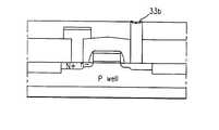
먼저, 반도체 기판(1)에 형성된 웰 영역(2)과, 웰 영역(2)의 소자 격리 영역에 형성된 소자 격리층(3)과, 상기 소자 격리층(3)에 의해 격리되는 활성 영역의 채널 영역상에 형성된 게이트 전극(5a)(5b)(5c)층과,게이트 전극(5a)(5b)(5c)을 마스크로한 불순물 이온주입 공정으로 형성된 불순물 확산 영역(소오스/드레인으로 사용되는)(4)과, 상기 게이트 전극들이 형성된 반도체 기판(1)의 전면에 콘택홀들을 갖고 형성된 제 1 층간 절연층(6)과, 상기 제 1 층간 절연층(6)의 콘택홀을 통하여 게이트 전극(5a)(5b)(5c)의 일측 불순물 확산 영역(4)에 콘택되는 폴리 실리콘 플러그층(7a),상기 폴리 실리콘 플러그층(7a)상에 형성된 실리사이드층(7b)으로 이루어진 비트 라인(7)과, 상기 비트 라인(7)을 포함하는 전면에 형성되는 제 2 층간 절연층(8)과, 상기 제 1,2 층간 절연층(6)(8)의 콘택홀을 통하여 상기 게이트 전극(5a)(5b)(5c)의 타측 불순물 확산 영역(4)에 콘택되는 폴리 실리콘 플러그층(9a),상기 폴리 실리콘 플러그층(9a)상에 차례로 적층되어 형성되는 베리어층(9b),금속 전극층(9c)으로 이루어진 커패시터 하부 전극층(9)을 포함하여 구성된다.First, the
상기와 같은 구조를 갖는 종래 기술의 반도체 소자의 커패시터에서는 커패시턴스를 높이기 위하여 고유전막을 사용하는데 고유전막 물질을 커패시터의 유전체로 사용할 경우에는 다음과 같은 제약에 이르게 된다.In the capacitor of the semiconductor device of the prior art having the above structure, a high dielectric film is used to increase the capacitance. When the high dielectric material is used as the dielectric of the capacitor, the following constraints are reached.
첫 번째는 폴리 실리콘층을 커패시터의 전극으로 사용할 경우에 폴리 실리콘 전극과 고유전체막 사이의 경계면에 실리콘 산화막이 형성되어 소자의 특성을 저하시키게 된다.First, when the polysilicon layer is used as the electrode of the capacitor, a silicon oxide film is formed on the interface between the polysilicon electrode and the high dielectric film, thereby degrading the device characteristics.
둘째로, 고유전체막의 증착 온도가 600 ∼700℃의 고온이므로 전극 물질을 고융점(High Melting Point)의 온도와 내산화성을 갖는 재료를 사용하여 형성해야 하므로 전극 재료의 선택에 제약을 받게된다. 즉, Pt,Pd,Rh,Ru,RuO2,IrO2등 산화가 되지 않는 금속이나 산화물을 전극으로 사용한다. 따라서 고유전체 물질을 커패시터의 유전 물질로 사용하려면 전극 구조의 개선과 그에 따른 공정 개발이 이루어져야 한다.Second, since the deposition temperature of the high-k dielectric film is 600 to 700 ° C., the electrode material must be formed using a material having a high melting point temperature and oxidation resistance, thereby limiting the selection of the electrode material. That is, metals or oxides that do not oxidize, such as Pt, Pd, Rh, Ru, RuO2 and IrO2 , are used as electrodes. Therefore, in order to use the high dielectric material as the dielectric material of the capacitor, the electrode structure should be improved and the process development accordingly.
종래 기술의 대표적인 전극 구조는 커패시터의 하부 전극과 반도체 기판의 불순물 영역을 연결하는 연결층의 구성이 다결정 실리콘을 사용하여 콘택 플러그층을 형성하고 그 위에 산화되지 않고 전도성이 양호한 금속 전극으로 Pt를 사용하는데, 이때 콘택 플러그층과 금속 도체(커패시터의 하부 전극)가 접촉하는 계면이 존재하므로써 금속을 증착하는 통상의 온도 범위에서도 이미 상당량의 실리사이드 핵이 금속과 실리콘이 반응하여 생길뿐만 아니라 증착 이후에 불가피한 열처리 공정(커패시터 유전막 증착,배선용 절연막 증착 등의)으로 인하여 쉽게 실리사이드화 반응이 생기게 되고 이 실리사이드화 반응은 하부 전극의 부피 변화를 수반하여 보이드,크랙 및 응력을 발생시킬 뿐만아니라 생성된 실리사이드는 쉽게 산화하는 특성을 가지고 있으므로 금속(하부 전극) 전체가 박리되는 등의 문제를 야기시키므로 그 대안으로 한층 또는 복수층의 산화 및 반응 방지막(Barrier Metal)을 사용해 오고 있다.The representative electrode structure of the prior art is that the connection layer connecting the lower electrode of the capacitor and the impurity region of the semiconductor substrate forms a contact plug layer using polycrystalline silicon and uses Pt as a metal electrode having good conductivity without being oxidized thereon. In this case, due to the presence of the interface between the contact plug layer and the metal conductor (lower electrode of the capacitor), a considerable amount of silicide nuclei are already generated by the reaction between the metal and silicon, and are unavoidable after the deposition even in the normal temperature range in which the metal is deposited. Due to the heat treatment process (capacitor dielectric film deposition, wiring insulation film deposition, etc.), a silicided reaction is easily generated, and the silicided reaction not only generates voids, cracks, and stresses along with the volume change of the lower electrode, but also the produced silicide is easily Having characteristics to oxidize As has been using metal (lower electrode), a further film or oxidation reaction, and a plurality of layers with an alternative because cause problems such as peeling off (Barrier Metal) overall.
그러나 이러한 베리어 메탈층은 공정 단가 및 복잡성을 증가 시킬뿐만 아니라 계면에서 원소들의 상호 확산을 완전히 제어하지 못한다.However, this barrier metal layer not only increases process cost and complexity, but also does not completely control the interdiffusion of elements at the interface.
본 발명은 상기와 같은 문제점을 해결하기 위하여 안출한 것으로, 공정 및 전극 구조를 단순화하고 커패시턴스를 효율적으로 향상시키는데 적당하도록한 반도체 소자의 커패시터 제조 방법을 제공하는데 그 목적이 있다.SUMMARY OF THE INVENTION The present invention has been made to solve the above problems, and an object thereof is to provide a method of manufacturing a capacitor of a semiconductor device, which is suitable for simplifying a process and an electrode structure and efficiently improving capacitance.
도 1은 종래 기술의 커패시터의 구조 단면도1 is a structural cross-sectional view of a conventional capacitor
도 2a내지 도 2i는 본 발명에 따른 커패시터 형성을 나타낸 공정 단면도2A to 2I are process cross-sectional views illustrating capacitor formation according to the present invention.
도 3a와 도 3b는 본 발명의 실시예에 따른 XRD 패턴을 나타낸 그래프3A and 3B are graphs showing an XRD pattern according to an embodiment of the present invention.
도면의 주요 부분에 대한 부호의 설명Explanation of symbols for the main parts of the drawings
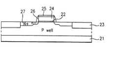
21. 반도체 기판 22. 게이트 절연막 23. 소자 격리막21.
24. 게이트 전극 25. 캡산화막 26. 게이트 측벽24.
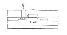
27. 소오스/드레인 영역 28. 제 1 층간 절연층 29. 콘택홀27. Source / drain
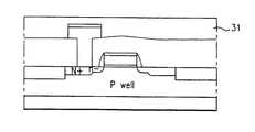
30a.30b. 비트 라인 31. 제 2 층간 절연층 32. 플러그층30a.30b. Bit line 31. Second
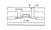
33a. Si-H 본딩층 33b. SiOx막 34. 하부 전극층33a. Si-
전극 구조를 단순화하고 커패시턴스를 향상시켜 양산체제에 효율적으로 적용할 수 있도록한 본 발명의 반도체 소자의 커패시터 제조 방법은 트랜지스터가 구비된 반도체 기판을 준비하는 단계,상기 트랜지스터의 불순물 영역과 전기적으로 연결되는 플러그를 형성하는 단계,상기 플러그의 표면에 Si-H 본딩층을 형성하는 단계,상기 Si-H 본딩층의 H이온을 탈착시켜 SiOx막을 형성하는 단계,상기 플러그위에 전극을 형성하는 단계를 포함하는 것을 특징으로 한다.In the method of manufacturing a capacitor of a semiconductor device of the present invention to simplify the electrode structure and improve capacitance, the method of manufacturing a semiconductor device of the present invention may include preparing a semiconductor substrate including a transistor and electrically connecting the impurity region of the transistor. Forming a plug, Forming a Si-H bonding layer on the surface of the plug, Desorption of H ions of the Si-H bonding layer to form a SiOx film, Forming an electrode on the plug It is characterized by.
이하, 첨부된 도면을 참고하여 본 발명의 반도체 소자의 커패시터의 제조 방법에 관하여 상세히 설명하면 다음과 같다.Hereinafter, a method of manufacturing a capacitor of a semiconductor device of the present invention will be described in detail with reference to the accompanying drawings.
도 2a내지 도 2i는 본 발명에 따른 커패시터 형성 방법을 나타낸 공정 단면도이고, 도 3a와 도 3b는 본 발명의 실시예에 따른 XRD(X-Ray Diffraction) 패턴을 나타낸 그래프이다.2A to 2I are cross-sectional views illustrating a method of forming a capacitor according to the present invention, and FIGS. 3A and 3B are graphs illustrating an X-ray diffraction (XRD) pattern according to an embodiment of the present invention.
본 발명은 고유전막 커패시터의 복잡한 전극 구조를 단순화하고 개선시키기 위한 것으로, 셀 트랜지스터의 소오스/드레인과 전기적으로 연결되는 다결정 실리콘 플러그와 커패시터의 하부 전극 사이에 확산 방지막 또는 다결정 실리콘의 산화 방지막의 역할을 하는 별도의 막을 사용하지 않고 고유전막을 갖는 커패시터를 구현하는 기술이다.The present invention simplifies and improves the complex electrode structure of a high-k dielectric capacitor, and serves as a diffusion barrier or an anti-oxidation film of polycrystalline silicon between a polycrystalline silicon plug electrically connected to a source / drain of a cell transistor and a lower electrode of the capacitor. It is a technique for implementing a capacitor having a high dielectric film without using a separate film.
본 발명의 반도체 소자의 커패시터의 제조 공정은 먼저, 도 2a에서와 같이, 웰이 형성된 반도체 기판(21)의 소자 격리 영역에 선택적으로 소자 격리막(23)을 형성한다.In the manufacturing process of the capacitor of the semiconductor device of the present invention, first, as shown in FIG. 2A, the
이어, 전기로에서 열산화 공정을 진행하여 웰이 형성된 반도체 기판(21)의 표면에 게이트 절연막(22)을 80Å(±10%)정도의 두께로 형성한다.Subsequently, a thermal oxidation process is performed in the electric furnace to form a
그리고 LPCVD(Low Pressure Chemical Vapour Deposition)방식으로 폴리 실리콘층 또는 비정질 실리콘층을 2000Å(±10%)두께로 성장시키고, 상기의 폴리 실리콘층 또는 비정질 실리콘층상에 LPCVD 방식으로 1500Å(±10%)정도의 두께로 산화막을 증착한다.In addition, a polysilicon layer or an amorphous silicon layer is grown to 2000Å (± 10%) thickness by LPCVD (Low Pressure Chemical Vapor Deposition) method, and about 1500Å (± 10%) by LPCVD method on the polysilicon layer or amorphous silicon layer. An oxide film is deposited to a thickness of.
이어, 사진 식각 방식으로 상기의 산화막과 폴리 실리콘층 또는 비정질 실리콘층을 선택적으로 식각하여 게이트 전극(24),캡산화막(25)층을 형성한다.Subsequently, the oxide layer and the polysilicon layer or the amorphous silicon layer are selectively etched by the photolithography method to form the
그리고 상기 게이트 전극(24)을 마스크로 저농도 불순물 확산 영역을 형성하기 위하여 P 이온을 2.4*1013/cm2,40KeV(±10%)의 조건으로 이온 주입하고 게이트 전극(24) 형성된 반도체 기판(21)의 전면에 불순물이 도핑되지 않은 산화막층을 형성하고 RIE(Reactive ion etching)공정으로 이방성 식각하여 상기의 패터닝된 게이트 전극(24)의 측면에 게이트 측벽(26)을 형성한다.In order to form a low concentration impurity diffusion region using the
이어, 상기의 게이트 측벽(26)이 형성된 게이트 전극(24)을 마스크로 하여 As+이온을 5*1015/cm2,40KeV(±10%)의 조건으로 이온 주입하여 고농도 불순물 확산 영역을 형성한다. 그리고 850℃,30min(±10%)의 조건으로 열처리하여 LDD(Lightly Doped Drain) 구조의 소오스/드레인 영역(27)을 형성한다.Subsequently, a high concentration impurity diffusion region is formed by ion implantation of As+ ions under a condition of 5 * 1015 / cm2 , 40 KeV (± 10%) using the
그리고 도 2b에서와 같이, 셀 트랜지스터들이 형성된 반도체 기판(21)의 전면에 4000Å(±10%)정도의 두께로 제 1 층간 절연층(28)을 형성한다. 이때, 상기의 제 1 층간 절연층(28)은 평탄화 특성이 좋은 BPSG(Boron Phosphorus Silicate Glass) 또는 TEOS(TetraEthylOrthoSilicate) 등의 물질을 사용하여 형성한다.As shown in FIG. 2B, the first
다음으로 도 2c에서와 같이, 상기의 제 1 층간 절연층(28)상에 포토레지스트층(도면에 도시하지 않음)을 형성하고 선택적으로 패터닝하여 패터닝된 포토레지스트층을 마스크로하여 상기의 제 1 층간 절연층(28)을 선택적으로 제거하여 콘택홀(29)을 형성한다. 상기 콘택홀(29)의 형성 공정은 RIE 방식으로 CHF3또는 CF4가스의 플라즈마를 이용하여 상기 제 1 층간 절연층(28)을 선택적으로 식각하여 반도체 기판(21)의 표면이 노출되도록 한다.Next, as shown in FIG. 2C, a photoresist layer (not shown) is formed on the first
이어, 도 2d에서와 같이, 상기의 콘택홀(29)을 포함하는 전면에 LPCVD 공정으로 다결정 실리콘 또는 비정질 실리콘을 2000Å(±10%)정도의 두께로 증착한다. 이어, 상기 다결정 실리콘 또는 비정질 실리콘층상에 화학 증착법으로 W 등의 고융점 금속을 이용한 금속 실리사이드를 1000Å(±10%)정도의 두께로 증착한다. 이때, 상기의 다결정 실리콘 또는 비정질 실리콘층은 셀 트랜지스터의 일측 불순물 확산 영역에 콘택된다.Subsequently, as shown in FIG. 2D, polycrystalline silicon or amorphous silicon is deposited on the entire surface including the
그리고 포토리소그래피공정으로 상기의 금속 실리사이드층 및 비정질 실리콘 또는 다결정 실리콘층을 선택적으로 식각하여 비트 라인(30a)(30b)을 형성한다.The metal silicide layer and the amorphous silicon or polycrystalline silicon layer are selectively etched by the photolithography process to form
이어, 도 2e에서와 같이, 상기의 비트 라인(30a)(30b)을 포함하는 전면에 TEOS 또는 BPSG 등의 물질을 6000Å(±10%)정도의 두께로 증착하여 제 2 층간 절연층(31)을 형성한다.Subsequently, as illustrated in FIG. 2E, a second interlayer insulating layer 31 is formed by depositing a material such as TEOS or BPSG to a thickness of about 6000 m (± 10%) on the entire surface including the
그리고 도 2f에서와 같이, 상기 셀 트랜지스터의 타측 불순물 확산 영역상의 제 1 층간 절연층(28),제 2 층간 절연층(31)을 선택적으로 제거하여 스토리지노드 콘택홀을 형성한다. 이때, 상기 스토리지노드 콘택홀을 형성하기 위한 제 1,2 층간 절연층(28)(31)의 식각 공정은 RIE공정으로 CHF3또는 CF4가스의 플라즈마를 이용하여 진행한다.2F, a storage node contact hole is formed by selectively removing the first
이어, 상기 스토리지노드 콘택홀을 포함하는 전면에 LPCVD 공정으로 다결정 실리콘 또는 비정질 실리콘을 1500Å(±10%)정도의 두께로 증착한다.Subsequently, polycrystalline silicon or amorphous silicon is deposited to a thickness of about 1500 kV (± 10%) on the front surface including the storage node contact hole by the LPCVD process.
그리고 도 2g에서와 같이, 상기의 다결정 실리콘층 또는 비정질 실리콘층을 에치백하여 커패시터의 하부 전극을 형성하기 위한 플러그층(32)을 형성한다.As shown in FIG. 2G, the polycrystalline silicon layer or the amorphous silicon layer is etched back to form a
상기의 플러그층(32) 표면의 Si원자의 댕글링 본드(Dangling bond)를 수소 원자로 마감시키기 위하여 HF 수용액에 담궈(Dipping) Si-H 본딩층(33a)을 실리콘 표면에 균일하게 만든다.In order to finish the dangling bond of Si atoms on the surface of the
이어, 도 2h에서와 같이, 금속막을 증착시키기 위한 진공 챔버에 웨이퍼를 넣고 압력을 1torr 이하로 유지시킨후 온도를 상온이상으로 가열하여 플러그층(32) 표면의 수소를 탈착시켜 SiOx막(33b)을 형성한다.Subsequently, as shown in FIG. 2H, the wafer is placed in a vacuum chamber for depositing a metal film, the pressure is maintained at 1 torr or less, and the temperature is maintained at room temperature or higher to desorb hydrogen on the surface of the
그리고 도 2i에서와 같이, 상기 SiOx막(33b)이 표면에 균일하게 형성된 플러그층(32)을 포함하는 전면에 Pt 또는 Ru 등의 금속막을 CVD, 스퍼터링(Sputtering), Evaporation 등의 방법으로 증착하고 선택적으로 식각하여 커패시터 영역을 한정하는 하부 전극층(34)을 형성한다.As shown in FIG. 2I, a metal film such as Pt or Ru is deposited on the entire surface of the
이어, 도면에 도시되지 않았지만, MOCVD법 또는 스퍼터링 공정으로 고 유전물질(BST,PZT,SBT 등의)층을 500Å(±10%)정도의 두께로 형성하고 1000Å(±10%)정도의 두께로 금속층을 형성하여 상부 전극층을 형성하여 커패시터를 완성하게 된다.Subsequently, although not shown in the drawings, a high dielectric material (BST, PZT, SBT, etc.) layer is formed to a thickness of about 500 kV (± 10%) by a MOCVD method or a sputtering process. The metal layer is formed to form the upper electrode layer to complete the capacitor.
상기의 SiOx막(33b)은 수소가 탈착되면 1torr 이하의 산소 분압하에 산소가 수소를 치환하여 단일막 형태로 생성되는 것이다. 이와 같이 생성된 SiOx막(33b)은 후속되는 공정 즉, 고,강유전막 증착 및 결정화 공정에서 요구되는 온도까지 안정하다.In the
상기와 같은 본 발명에 따른 반도체 소자의 커패시터 제조 방법은 다결정 실리콘 또는 비정질 실리콘 등의 형성한 플러그층(32)의 표면을 HF 처리하여 상기 플러그층(32)의 표면에 Si-H 본딩층(33a)을 형성하여 수소 원자로 마감시켜 저온의 진공 분위기에서는 산화 방지막으로 이용하고 금속을 증착하는 공정 온도에서는 Si-H 본딩층(33a)이 파괴되어 H 보다 Si와 결합 친화력이 큰 O가 H를 대신하여 단층 또는 이중층의 SiOx막(33b)을 형성하는 것이다.In the method of manufacturing a capacitor of a semiconductor device according to the present invention as described above, the Si-
이 막은 이후 산화 분위기에서 급격하게 진행되는 산화 반응을 억제하는 역할을 하게된다.This film then serves to suppress the oxidation reaction that proceeds rapidly in the oxidizing atmosphere.
또한, 고,강유전막을 결정시키거나 평탄화를 위한 글래스 리플로우(Glass Reflow)등에서 요구되는 750℃ 이상의 온도로 열처리를 하면 계면의 SiOx막(33b)은 파괴되어 다결정 실리콘등으로 이루어진 플러그층(32)과 금속간에 도통을 보장해준다.In addition, when the high ferroelectric film is crystallized or heat-treated at a temperature of 750 ° C. or higher required for glass reflow for planarization, the
상기와 같은 본 발명의 SiOx막(33b)은 자연산화막에서 발생하는 두께 조절의 문제,전기적 도통의 문제가 없다.The
도 3a는 플러그층을 형성하고 300℃의 온도에서 직접 Ru를 증착하고 650℃의 온도에서 30분간 열처리한후의 XRD 패턴을 나타낸 것이고, 도 3b는 플러그층을 형성하고 600℃까지 가열하여 수소를 탈착시킨후 300℃(±10%)에서 Ru를 증착하고 650℃,30분간 열처리한후의 XRD 패턴을 나타낸 그래프이다. 여기서, XRD(X-Ray Diffraction)패턴이란 계면 반응에 의하여 생긴 새로운 결정상과 하부 전극 금 속의 방향성을 조사하기 위한 것으로, 도 3a와 도 3b의 X축은 X-Ray의 입사각(2θ)을 나타내며,Y축은 X-Ray의 회절 강도(Diffraction Intensity)를 나타낸다.Figure 3a shows the XRD pattern after forming a plug layer and directly depositing Ru at a temperature of 300 ℃ and heat-treated at a temperature of 650 ℃ 30 minutes, Figure 3b is a plug layer formed and heated to 600 ℃ desorption hydrogen After the deposition of Ru at 300 ℃ (± 10%) and a heat treatment at 650 ℃, 30 minutes is a graph showing the XRD pattern. Here, the X-Ray Diffraction (XRD) pattern is used to investigate the directivity of the new crystal phase and the lower electrode metal caused by the interfacial reaction. The X-axis of FIGS. 3A and 3B represents an incident angle (2θ) of X-Ray. The axis represents the diffraction intensity of the X-ray.
도 3a의 30.7도 부근에서는 실리사이드의 존재가 나타나고 있으나 도 3b에서는 보이지 않고 42.2도 부근의 (002) 결정이 잘 발달되는 특징으로 보여 주고 있다. 이와 같이 도 3b에서 나타난 42.2도 부근의 (002)결정은 후속되는 공정에서의 고유전막의 결정 성장에도 좋은 영향을 미치게 된다.The presence of silicide is shown in the vicinity of 30.7 degrees in FIG. 3A, but it is not seen in FIG. 3B, but shows that the (002) crystal in the vicinity of 42.2 degrees is well developed. As such, the (002) crystal near 42.2 degrees shown in FIG. 3B has a good effect on the crystal growth of the high dielectric film in a subsequent process.
다결정 콘택 플러그층과 커패시터의 하부 전극의 계면에서 발생하는 콘택 불량의 문제를 그 계면에 SiOx막을 게재(揭載)하여 해결한 본발명의 반도체 소자의 커패시터의 제조 방법은 한층 또는 복수층의 산화 및 반응 방지막(Barrier Metal)을 사용하는 기술에 비해 공정 단가를 감소시키고, 공정을 단순화하는 효과가 있다.The method of manufacturing the capacitor of the semiconductor device of the present invention, which solves the problem of contact failure occurring at the interface between the polycrystalline contact plug layer and the lower electrode of the capacitor by placing an SiOx film at the interface, is characterized by one or more layers of oxidation and Compared to a technology using a barrier metal, the process cost is reduced and the process is simplified.
또한, 계면에서의 원소들의 상호 확산을 완전히 제어할 수 있어 소자의 신뢰성을 높이고 공정 마진을 높이는 효과가 있다. 즉, 공정 및 전극 구조를 단순화하고 커패시턴스를 효율적으로 향상시키는 효과가 있다.In addition, the mutual diffusion of the elements at the interface can be completely controlled to increase the reliability of the device and increase the process margin. That is, there is an effect of simplifying the process and the electrode structure and efficiently improving the capacitance.
Claims (14)
Translated fromKoreanPriority Applications (5)
| Application Number | Priority Date | Filing Date | Title |
|---|---|---|---|
| KR1019970035826AKR100244306B1 (en) | 1997-07-29 | 1997-07-29 | Method for forming capacitor of semiconductor divice |
| TW086115758ATW374944B (en) | 1997-07-29 | 1997-10-24 | Method of manufacture of semiconductor capacitors |
| US08/961,265US5918123A (en) | 1997-07-29 | 1997-10-30 | Method for fabricating capacitor of semiconductor device |
| JP10031679AJP2886524B2 (en) | 1997-07-29 | 1998-02-13 | Method of manufacturing capacitor for semiconductor device |
| DE19824774ADE19824774C2 (en) | 1997-07-29 | 1998-06-03 | Method of manufacturing a capacitor in a semiconductor device |
Applications Claiming Priority (1)
| Application Number | Priority Date | Filing Date | Title |
|---|---|---|---|
| KR1019970035826AKR100244306B1 (en) | 1997-07-29 | 1997-07-29 | Method for forming capacitor of semiconductor divice |
Publications (2)
| Publication Number | Publication Date |
|---|---|
| KR19990012435A KR19990012435A (en) | 1999-02-25 |
| KR100244306B1true KR100244306B1 (en) | 2000-02-01 |
Family
ID=19516103
Family Applications (1)
| Application Number | Title | Priority Date | Filing Date |
|---|---|---|---|
| KR1019970035826AExpired - Fee RelatedKR100244306B1 (en) | 1997-07-29 | 1997-07-29 | Method for forming capacitor of semiconductor divice |
Country Status (5)
| Country | Link |
|---|---|
| US (1) | US5918123A (en) |
| JP (1) | JP2886524B2 (en) |
| KR (1) | KR100244306B1 (en) |
| DE (1) | DE19824774C2 (en) |
| TW (1) | TW374944B (en) |
Families Citing this family (9)
| Publication number | Priority date | Publication date | Assignee | Title |
|---|---|---|---|---|
| US6787186B1 (en)* | 1997-12-18 | 2004-09-07 | Advanced Technology Materials, Inc. | Method of controlled chemical vapor deposition of a metal oxide ceramic layer |
| KR100533991B1 (en)* | 1997-12-27 | 2006-05-16 | 주식회사 하이닉스반도체 | Manufacturing method of high dielectric capacitor of semiconductor device |
| US6075264A (en) | 1999-01-25 | 2000-06-13 | Samsung Electronics Co., Ltd. | Structure of a ferroelectric memory cell and method of fabricating it |
| US6412786B1 (en)* | 1999-11-24 | 2002-07-02 | United Microelectronics Corp. | Die seal ring |
| US6297123B1 (en)* | 2000-11-29 | 2001-10-02 | United Microelectronics Corp. | Method of preventing neck oxidation of a storage node |
| KR100455725B1 (en)* | 2001-10-08 | 2004-11-12 | 주식회사 하이닉스반도체 | Method for forming plug in semiconductor device |
| US7858471B2 (en)* | 2006-09-13 | 2010-12-28 | Micron Technology, Inc. | Methods of fabricating an access transistor for an integrated circuit device, methods of fabricating periphery transistors and access transistors, and methods of fabricating an access device comprising access transistors in an access circuitry region and peripheral transistors in a peripheral circuitry region spaced from the access circuitry region |
| JP4645641B2 (en)* | 2007-12-03 | 2011-03-09 | 富士電機システムズ株式会社 | Method for manufacturing SiC Schottky diode |
| US8518811B2 (en)* | 2011-04-08 | 2013-08-27 | Infineon Technologies Ag | Schottky diodes having metal gate electrodes and methods of formation thereof |
Family Cites Families (3)
| Publication number | Priority date | Publication date | Assignee | Title |
|---|---|---|---|---|
| TW243541B (en)* | 1991-08-31 | 1995-03-21 | Samsung Electronics Co Ltd | |
| JP3197782B2 (en)* | 1994-04-29 | 2001-08-13 | インターナショナル・ビジネス・マシーンズ・コーポレ−ション | Semiconductor integrated circuit capacitor and its electrode structure |
| JP2689935B2 (en)* | 1995-02-01 | 1997-12-10 | 日本電気株式会社 | Semiconductor thin film forming method |
- 1997
- 1997-07-29KRKR1019970035826Apatent/KR100244306B1/ennot_activeExpired - Fee Related
- 1997-10-24TWTW086115758Apatent/TW374944B/ennot_activeIP Right Cessation
- 1997-10-30USUS08/961,265patent/US5918123A/ennot_activeExpired - Lifetime
- 1998
- 1998-02-13JPJP10031679Apatent/JP2886524B2/ennot_activeExpired - Fee Related
- 1998-06-03DEDE19824774Apatent/DE19824774C2/ennot_activeExpired - Fee Related
Also Published As
| Publication number | Publication date |
|---|---|
| KR19990012435A (en) | 1999-02-25 |
| JP2886524B2 (en) | 1999-04-26 |
| JPH1154729A (en) | 1999-02-26 |
| US5918123A (en) | 1999-06-29 |
| DE19824774C2 (en) | 2002-08-08 |
| DE19824774A1 (en) | 1999-02-25 |
| TW374944B (en) | 1999-11-21 |
Similar Documents
| Publication | Publication Date | Title |
|---|---|---|
| US5702970A (en) | Method for fabricating a capacitor of a semiconductor device | |
| JP4111427B2 (en) | Capacitor manufacturing method for semiconductor device | |
| US5953619A (en) | Semiconductor device with perovskite capacitor and its manufacture method | |
| KR100244306B1 (en) | Method for forming capacitor of semiconductor divice | |
| US6319765B1 (en) | Method for fabricating a memory device with a high dielectric capacitor | |
| KR100458084B1 (en) | Ferroelectric Capacitor Formation Method with Lower Electrode with Reduced Leakage Current | |
| KR100355777B1 (en) | Ferroelectric capacitor formed under the bit line | |
| KR100402943B1 (en) | High dielectric capacitor and a method of manufacturing the same | |
| JP2002190580A (en) | Semiconductor device and method of manufacturing the same | |
| US6306666B1 (en) | Method for fabricating ferroelectric memory device | |
| US6511880B2 (en) | Capacitor of a semiconductor device and method of manufacturing the same | |
| KR100436057B1 (en) | Manufacturing method of high dielectric capacitor of semiconductor device | |
| KR0180786B1 (en) | Capacitor Formation Method of Semiconductor Device | |
| KR100414737B1 (en) | manufacturing method for capacitor of semiconductor device | |
| KR100448243B1 (en) | Method for fabricating capacitor | |
| JP4162879B2 (en) | Manufacturing method of semiconductor device | |
| KR20010027082A (en) | Method of manufacturing a capacitor in a semiconductor device | |
| KR100574473B1 (en) | Capacitor Manufacturing Method of Semiconductor Device_ | |
| KR100883136B1 (en) | Ferroelectric memory device having an open diffusion barrier film structure and manufacturing method thereof | |
| KR100504434B1 (en) | Method of forming capacitor | |
| KR100646947B1 (en) | Capacitor manufacturing method of semiconductor device | |
| KR100580747B1 (en) | Manufacturing method of high dielectric capacitor | |
| KR100447981B1 (en) | Capacitors in Semiconductor Devices and Manufacturing Methods Thereof | |
| KR20020015421A (en) | Method of manufacturing a high dielectric capacitor | |
| JP2002033461A (en) | Semiconductor device and method of manufacturing the same |
Legal Events
| Date | Code | Title | Description |
|---|---|---|---|
| A201 | Request for examination | ||
| PA0109 | Patent application | St.27 status event code:A-0-1-A10-A12-nap-PA0109 | |
| PA0201 | Request for examination | St.27 status event code:A-1-2-D10-D11-exm-PA0201 | |
| R17-X000 | Change to representative recorded | St.27 status event code:A-3-3-R10-R17-oth-X000 | |
| P11-X000 | Amendment of application requested | St.27 status event code:A-2-2-P10-P11-nap-X000 | |
| P13-X000 | Application amended | St.27 status event code:A-2-2-P10-P13-nap-X000 | |
| PG1501 | Laying open of application | St.27 status event code:A-1-1-Q10-Q12-nap-PG1501 | |
| PN2301 | Change of applicant | St.27 status event code:A-3-3-R10-R13-asn-PN2301 St.27 status event code:A-3-3-R10-R11-asn-PN2301 | |
| E701 | Decision to grant or registration of patent right | ||
| PE0701 | Decision of registration | St.27 status event code:A-1-2-D10-D22-exm-PE0701 | |
| GRNT | Written decision to grant | ||
| PR0701 | Registration of establishment | St.27 status event code:A-2-4-F10-F11-exm-PR0701 | |
| PR1002 | Payment of registration fee | St.27 status event code:A-2-2-U10-U11-oth-PR1002 Fee payment year number:1 | |
| PG1601 | Publication of registration | St.27 status event code:A-4-4-Q10-Q13-nap-PG1601 | |
| PR1001 | Payment of annual fee | St.27 status event code:A-4-4-U10-U11-oth-PR1001 Fee payment year number:4 | |
| PR1001 | Payment of annual fee | St.27 status event code:A-4-4-U10-U11-oth-PR1001 Fee payment year number:5 | |
| PR1001 | Payment of annual fee | St.27 status event code:A-4-4-U10-U11-oth-PR1001 Fee payment year number:6 | |
| PR1001 | Payment of annual fee | St.27 status event code:A-4-4-U10-U11-oth-PR1001 Fee payment year number:7 | |
| PR1001 | Payment of annual fee | St.27 status event code:A-4-4-U10-U11-oth-PR1001 Fee payment year number:8 | |
| PR1001 | Payment of annual fee | St.27 status event code:A-4-4-U10-U11-oth-PR1001 Fee payment year number:9 | |
| PR1001 | Payment of annual fee | St.27 status event code:A-4-4-U10-U11-oth-PR1001 Fee payment year number:10 | |
| FPAY | Annual fee payment | Payment date:20091028 Year of fee payment:11 | |
| PR1001 | Payment of annual fee | St.27 status event code:A-4-4-U10-U11-oth-PR1001 Fee payment year number:11 | |
| LAPS | Lapse due to unpaid annual fee | ||
| PC1903 | Unpaid annual fee | St.27 status event code:A-4-4-U10-U13-oth-PC1903 Not in force date:20101123 Payment event data comment text:Termination Category : DEFAULT_OF_REGISTRATION_FEE | |
| PC1903 | Unpaid annual fee | St.27 status event code:N-4-6-H10-H13-oth-PC1903 Ip right cessation event data comment text:Termination Category : DEFAULT_OF_REGISTRATION_FEE Not in force date:20101123 | |
| P22-X000 | Classification modified | St.27 status event code:A-4-4-P10-P22-nap-X000 |