KR100242274B1 - Floating point / integer processor with division and square root calculations - Google Patents
Floating point / integer processor with division and square root calculationsDownload PDFInfo
- Publication number
- KR100242274B1 KR100242274B1KR1019890000957AKR890000957AKR100242274B1KR 100242274 B1KR100242274 B1KR 100242274B1KR 1019890000957 AKR1019890000957 AKR 1019890000957AKR 890000957 AKR890000957 AKR 890000957AKR 100242274 B1KR100242274 B1KR 100242274B1
- Authority
- KR
- South Korea
- Prior art keywords
- register
- multiplier
- circuit
- square root
- product
- Prior art date
- Legal status (The legal status is an assumption and is not a legal conclusion. Google has not performed a legal analysis and makes no representation as to the accuracy of the status listed.)
- Expired - Lifetime
Links
Images


Classifications
- G—PHYSICS
- G06—COMPUTING OR CALCULATING; COUNTING
- G06F—ELECTRIC DIGITAL DATA PROCESSING
- G06F7/00—Methods or arrangements for processing data by operating upon the order or content of the data handled
- G06F7/38—Methods or arrangements for performing computations using exclusively denominational number representation, e.g. using binary, ternary, decimal representation
- G06F7/48—Methods or arrangements for performing computations using exclusively denominational number representation, e.g. using binary, ternary, decimal representation using non-contact-making devices, e.g. tube, solid state device; using unspecified devices
- G06F7/52—Multiplying; Dividing
- G06F7/535—Dividing only
- G—PHYSICS
- G06—COMPUTING OR CALCULATING; COUNTING
- G06F—ELECTRIC DIGITAL DATA PROCESSING
- G06F7/00—Methods or arrangements for processing data by operating upon the order or content of the data handled
- G06F7/38—Methods or arrangements for performing computations using exclusively denominational number representation, e.g. using binary, ternary, decimal representation
- G06F7/48—Methods or arrangements for performing computations using exclusively denominational number representation, e.g. using binary, ternary, decimal representation using non-contact-making devices, e.g. tube, solid state device; using unspecified devices
- G06F7/4824—Methods or arrangements for performing computations using exclusively denominational number representation, e.g. using binary, ternary, decimal representation using non-contact-making devices, e.g. tube, solid state device; using unspecified devices using signed-digit representation
- G—PHYSICS
- G06—COMPUTING OR CALCULATING; COUNTING
- G06F—ELECTRIC DIGITAL DATA PROCESSING
- G06F7/00—Methods or arrangements for processing data by operating upon the order or content of the data handled
- G06F7/38—Methods or arrangements for performing computations using exclusively denominational number representation, e.g. using binary, ternary, decimal representation
- G06F7/48—Methods or arrangements for performing computations using exclusively denominational number representation, e.g. using binary, ternary, decimal representation using non-contact-making devices, e.g. tube, solid state device; using unspecified devices
- G06F7/544—Methods or arrangements for performing computations using exclusively denominational number representation, e.g. using binary, ternary, decimal representation using non-contact-making devices, e.g. tube, solid state device; using unspecified devices for evaluating functions by calculation
- G06F7/552—Powers or roots, e.g. Pythagorean sums
- G06F7/5525—Roots or inverse roots of single operands
- G—PHYSICS
- G06—COMPUTING OR CALCULATING; COUNTING
- G06F—ELECTRIC DIGITAL DATA PROCESSING
- G06F2207/00—Indexing scheme relating to methods or arrangements for processing data by operating upon the order or content of the data handled
- G06F2207/535—Indexing scheme relating to groups G06F7/535 - G06F7/5375
- G06F2207/5355—Using iterative approximation not using digit recurrence, e.g. Newton Raphson or Goldschmidt
- G—PHYSICS
- G06—COMPUTING OR CALCULATING; COUNTING
- G06F—ELECTRIC DIGITAL DATA PROCESSING
- G06F7/00—Methods or arrangements for processing data by operating upon the order or content of the data handled
- G06F7/38—Methods or arrangements for performing computations using exclusively denominational number representation, e.g. using binary, ternary, decimal representation
- G06F7/48—Methods or arrangements for performing computations using exclusively denominational number representation, e.g. using binary, ternary, decimal representation using non-contact-making devices, e.g. tube, solid state device; using unspecified devices
- G06F7/483—Computations with numbers represented by a non-linear combination of denominational numbers, e.g. rational numbers, logarithmic number system or floating-point numbers
- G06F7/487—Multiplying; Dividing
- G06F7/4873—Dividing
- G—PHYSICS
- G06—COMPUTING OR CALCULATING; COUNTING
- G06F—ELECTRIC DIGITAL DATA PROCESSING
- G06F7/00—Methods or arrangements for processing data by operating upon the order or content of the data handled
- G06F7/38—Methods or arrangements for performing computations using exclusively denominational number representation, e.g. using binary, ternary, decimal representation
- G06F7/48—Methods or arrangements for performing computations using exclusively denominational number representation, e.g. using binary, ternary, decimal representation using non-contact-making devices, e.g. tube, solid state device; using unspecified devices
- G06F7/499—Denomination or exception handling, e.g. rounding or overflow
- G06F7/49942—Significance control
- G06F7/49947—Rounding
- G06F7/49957—Implementation of IEEE-754 Standard
Landscapes
- Physics & Mathematics (AREA)
- General Physics & Mathematics (AREA)
- Engineering & Computer Science (AREA)
- Computational Mathematics (AREA)
- Mathematical Analysis (AREA)
- Pure & Applied Mathematics (AREA)
- Theoretical Computer Science (AREA)
- Mathematical Optimization (AREA)
- Computing Systems (AREA)
- General Engineering & Computer Science (AREA)
- Complex Calculations (AREA)
Abstract
Translated fromKoreanDescription
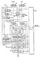
Translated fromKorean제1도는 본 발명의 프로세서 구조를 도시한 도면.1 is a diagram illustrating a processor structure of the present invention.
제2도는 제산 및 제곱근 계산시에 사용된 회로의 상세한 블럭도.2 is a detailed block diagram of the circuit used in the division and square root calculations.
* 도면의 주요부분에 대한 부호의 설명* Explanation of symbols for main parts of the drawings
10 : 프로세서 12 : 입력 스테이지10
14 : 계산 스테이지 16 : 출력스테이지14: calculation stage 16: output stage
18 : 임시 레지스터 22a-b : 패리티 검사기18: temporary register 22a-b: parity checker
28 : 구성 논리 회로 32 : A 입력 레지스터28: configuration logic circuit 32: A input register
34 : B 입력 레지스터 40,42,44,46,68,70 : 멀티플렉서34:
48 : 승산기 50, 56 : 파이프라인 레지스터48: multiplier 50, 56: pipeline register
52 : 변환기/끝수 처리기 54 : ALU52: converter / end processor 54: ALU
58 : 정규화기 60 : 명령 레지스터58: normalizer 60: instruction register
64 : 곱 레지스터 66 : 합 레지스터64: product register 66: sum register
70 : Y 멀티플렉서 76 : C 레지스터70: Y multiplexer 76: C register
80 : 상태 레지스터 82 : 패리티 발생기80: status register 82: parity generator
84 : 마스터/슬레이브 비교 회로 86, 88, 90 : 버퍼84: master /
102 : 상태기 104 : 제산/제곱근 회로102: state machine 104: division / square root circuit
106 : 섀도우 C 레지스터 108 : 시드 발생기106: shadow C register 108: seed generator
116 : 부호화 디지트 승산기 어레이 118 : 비교 레지스터116: coded digit multiplier array 118: comparison register
120 : 비교 논리 회로 122 : 보정 발생기120: comparison logic circuit 122: correction generator
본 발명은 주로 집적 회로에 관한 것으로, 특히 효율적인 제산 및 제곱근 계산 기능을 갖고 있는 프로세서에 관한 것이다.The present invention relates mainly to integrated circuits, and more particularly to a processor having efficient division and square root calculation functions.
고속 계산은, 컴퓨터, 신호 프로세서 및 프로세스 제어기와 같은 여러 시스템에서의 중요한 설계 요인이다. 이 시스템들은 고속 계산을 제공하기 위해 고도의 병렬 설계를 사용하는 LSI 집적 회로에 점점 의존하고 있다. 병렬 기법을 사용하여 정수 및 부동 소숫점 승산을 수행하는 특수화된 집적 회로들이 널리 사용되고 있다. 그러나, 제산 및 제곱근 기능을 수행하는 집적 회로들은 본질적으로 직렬이므로, 이들의 효과를 감소시키게 된다.High speed computation is an important design factor in many systems such as computers, signal processors and process controllers. These systems are increasingly turning to LSI integrated circuits that use highly parallel designs to provide high speed computation. Specialized integrated circuits that perform integer and floating point multiplication using parallel techniques are widely used. However, integrated circuits that perform division and square root functions are essentially in series, thus reducing their effects.
제산은 공지된 수렴(convergence) 알고리즘을 사용함으로써 다른 회로와 함께 고속 승산기에 의해 수행될 수 있다. 일반적으로, 고속 병렬 승산기들은 2개의 주요부로 나뉘어질 수 있다. 제1부는, 부분곱 발생기 및 부분곱을 합 및 캐리 스트림으로 환산하는 가산기 어레이를 포함한다. 제2부는 캐리와 합 스트림을 합산하는 최종 가산기를 포함한다. 제2부에 캐리 체인(carry chain)이 포함되기 때문에, 최종 가산은 부분곱 발생 및 가산과 거의 동일한 시간량을 소비한다. 때때로, 승산기의 처리 능력을 증가시키기 위해 2개의 부분(half)들 사이에 파이프라인 레지스터를 삽입하는데, 그 이유는 제2부가 최초 계산을 완료하는 동안에 제1부가 다음 동작을 개시할 수 있기 때문이다.Division may be performed by a high speed multiplier along with other circuits by using known convergence algorithms. In general, high speed parallel multipliers can be divided into two main parts. The first part includes a partial product generator and an array of adders that convert the partial products into sums and carry streams. The second part includes a final adder that sums the carry and sum streams. Since the carry chain is included in the second part, the final addition consumes almost the same amount of time as the partial product generation and addition. Sometimes, a pipeline register is inserted between two halves to increase the multiplier's processing power, since the first part may start the next operation while the second part completes the initial calculation. .
그 결과, 고속 병렬 승산기는 수렴 알고리즘의 반복시마다 최소한 3개의 클럭 사이클을 필요로 한다. 그리므로, 제산 및 제곱근 계산은 다른 계산에 비해 상당한 시간량을 필요로 한다.As a result, the fast parallel multiplier requires at least three clock cycles for each iteration of the convergence algorithm. Therefore, division and square root calculations require a significant amount of time compared to other calculations.
그러므로, 고속 제산 및 제곱근 계산을 할 수 있는 프로세서가 업계에서 요구되고 있다.Therefore, there is a need in the industry for a processor capable of fast division and square root calculations.
본 발명에 따르면. 종래의 제산 및 제곱근 계산에 관련된 단점 및 문제점을 거의 제거하거나 방지하는 프로세서가 제공된다.According to the invention. A processor is provided that substantially eliminates or avoids the disadvantages and problems associated with conventional division and square root calculations.
본 발명의 프로세서는 부분곱들의 합(sum of partial product)을 발생시키기 위한 제1 어레이부를 구비한 승산기를 포함한다. 승산기의 제2부는 제1부의 출력을 선정된 수치 표현으로 변환시키도록 작동된다. 변환기 회로에 관련된 지연을 방지 하기 위해서, 피드백 회로가 제1부의 출력을 승산기 입력에 접속시킨다. 양호한 실시예에 따르면, 제1 어레이부는 부호화 디지트 승산기 어레이(signed digit multiplication array)를 포함한다.The processor of the present invention includes a multiplier having a first array portion for generating a sum of partial products. The second part of the multiplier is operative to convert the output of the first part into a predetermined numerical representation. In order to prevent delays associated with the converter circuit, the feedback circuit connects the output of the first part to the multiplier input. According to a preferred embodiment, the first array portion comprises a signed digit multiplication array.
본 발명의 이러한 특징으로 인해 제산 및 제곱근 계산을 수행할 때 종래의 프로세서에 관련된 지연이 제거되므로, 본 발명은 짧은 시간에 결과를 발생시킬 수 있다는 기술적 장점을 제공한다This feature of the present invention provides a technical advantage that the present invention can produce results in a short time since the delay associated with conventional processors is eliminated when performing division and square root calculations.
본 발명의 제2 특징에 따르면, 승산기의 제1부와 제2부 사이에 보정 발생기(correction generator)를 두어 제1부에서 수행되고 있는 승산과 병행하여 다음 근사 계산에 사용될 수를 발생시킨다. 본 발명의 이 특징은 프로세싱 속도를 증가시킨다는 기술적 장점을 제공한다.According to a second aspect of the invention, a correction generator is placed between the first and second parts of the multiplier to generate a number to be used for the next approximation calculation in parallel with the multiplication being performed in the first part. This feature of the present invention provides the technical advantage of increasing the processing speed.
본 발명의 제3 특징에 따르면, 비교 회로론 제공하여 제산 계산 또는 제곱근 계산의 최종 근사치가 끝수 처리되어야 할 방향을 신속히 판단한다. 제산 계산의 경우에, 몫의 최종 근사치에 젯수를 승산하고, 이를 피젯수와 비교한다. 끝수 처리 방향은 피젯수가 계산된 곱보다 큰지, 작은지, 또는 같은지의 여부에 따라 달라질 수 있다. 제곱근의 경우에, 제곱근의 최종 근사치를 제곱 계산하고, 이를 피연산자와 비교한다. 끝수 처리는 피연산수가 근사 제곱근의 제곱보다 큰지, 작은지, 또는 같은지의 여부에 따라 달라질 수 있다.According to a third aspect of the present invention, a comparison circuit theory is provided to quickly determine the direction in which the final approximation of the division calculation or the square root calculation should be processed to the end. In the case of division calculation, the final approximation of the quotient is multiplied by the number of jets and compared with the number of pidgets. The fraction processing direction may vary depending on whether the pidget number is greater than, less than, or equal to the calculated product. In the case of the square root, the final approximation of the square root is squared and compared with the operands. Fractional processing may vary depending on whether the operand is greater than, less than, or equal to the square of the approximate square root.
피연산자의 최하위 비트만을 근사치의 대응 비트 및 어느 한 쪽의 가드(guard) 비트와 비교하기 때문에, 본 발명은 이러한 특징은 최종 근사치의 끝수 처리를 최소의 비교 회로로 신속히 수행할 수 있다는 기술적 장점을 제공한다.Since only the least significant bit of the operand is compared with the corresponding bit of the approximation and the guard bit on either side, this feature provides the technical advantage that the fractional processing of the final approximation can be performed quickly with minimal comparison circuitry. do.
이하, 첨부 도면을 참조하여 본 발명에 대해 상세히 설명하겠다.Hereinafter, the present invention will be described in detail with reference to the accompanying drawings.
본 발명의 양호한 실시예는 도면들 중 제1도 및 제2도를 참조함으로써 가장 양호하게 이해되는데, 도면들 내의 동일하고 대응하는 부분에는 동일한 참조번호를 이용하였다.The preferred embodiment of the present invention is best understood by referring to FIGS. 1 and 2 of the drawings, wherein like reference numerals are used for like and corresponding parts in the drawings.
제1도는 본 발명의 프로세서의 회로도를 도시한 것이다. 본 발명의 프로세서(10)은 3개의 스테이지, 즉 입력 스테이지(12), 계산 스테이지(14) 및 출력 스테이지(16)으로 도시되어 있다. 입력 스테이지는 A 입력 데이타 버스(20a) 및 B 입력 데이타 버스(20b)로 구성된 입력 데이타 버스(20)에 접속되는 임시 레지스터(18)을 포함한다. 패리티 검사기(22a, 22b)는 각각 입력 데이타 버스(20a, 20b) 및 패리티 라인(24a, 24b)에 접속된다. 패리티 애러 라인(26a, 26b)는 패리티 검사기(22a, 22b)로부티 출력된다. 또한, 입력 데이타 버스(20a, 20b)는 임시 레지스터(18)의 출력들과 함께 구성 논리 회로(28)에 접속된다. 구성 제어 신호(30) 및 “클럭 모드”신호(31)은 구성 논리 회로(28)에 입력된다.1 shows a circuit diagram of a processor of the present invention. The
구성 논리 회로(28)의 출력은 A 및 B 입력 레지스터(32 및 34)에 접속된다. 인에이블 신호 라인(36 및 38)은 A 입력 레지스터(3B) 및 B 입력 레지스터(34)에 각각 접속된다. A 및 B 입력 레지스터(32 및 34)는 일련의 멀티플렉서(40,42,44 및 46)에 접속된다. A 입력 레지스터(32)는 멀티플렉서(40) 및 멀티플렉서(44)에 접속되고, B 입력 레지스터(34)는 멀티플렉서(42) 및 멀티플렉서(46)에 접속된다. 멀티플렉서(40 및 42)의 출력은 파이프라인 레지스터(50) 및 변환기/끝수 처리기(52)를 갖고 있는 승산기(48)에 입력된다. 멀티플렉서(44 및 46)은 파이프라인 레지스터(56) 및 정규화기(normalizer, 58)을 갖고 있는 ALU(54)에 접속된다. 승산기(48) 및 ALU(54)는 명령 버스(62)에 접속되는 명령 레지스터(60)에 접속된다. 승산기(48)의 출력은 곱 레지스터(64)에 접속되고, ALU(54)의 출력은 합 레지스터(66)에 접속된다. 곱 레지스터(64) 및 합 레지스터(66)의 출력들은 멀티플렉서(68 및 70)에 접속된다. 또한, 곱 레지스터(64)의 출력은 멀티플렉서(42 및 44)에 접속되고, 합 레지스터(66)의 출력은 멀티플렉서(40 및 46)에 접속된다. 멀티플렉서(68 및 70)은 각각 제어 신호 라인(72 및 74)에 접속된다.The output of the
멀티플렉서(68)의 출력은 C 레지스터(76)에 접속된다. C 레지스터(76)의 출력은 멀티플렉서(40 내지 46)에 접속된다. C 레지스터(76)은 클럭 신호 라인(78)에 접속된다.The output of the
출력 스테이지(16)은 Y 멀티플렉서(70), 상태 레지스터(80), 패리티 발생기(82), 및 마스터/슬레이브 비교 회로(84)를 포함한다. 멀티플렉서(70)의 출력은 패리티 발생기(82), 마스터/슬레이브 비교 회로(84), 및 버퍼(86)에 접속된다. 상태 레지스터(80)은 마스터/ 슬레이브 비교 회로(84) 및 버퍼(88 및 90)에 접속된다. 버퍼(86)의 출력은 출력 데이타 버스(92) 및 마스터/ 슬레이브 비교 회로(84)에 접속된다. 버퍼(88 및 90)의 출력은 상태 버스(94)에 접속된다. 버퍼(86 내지 90)은 각각 제어라인(96, 98 및 100)에 의해 제어된다.
상태기(state machine, 102)는 [A 및 B 입력 레지스터(32 및 34) 및 멀티플렉서(40 내지 46)에 접속될 뿐만 아니라 (이 접속 상태는 도시되어 있지 않음)] 승산기(48) 및 제산/제곱근 회로(104)에 접속된다. 또한, 제산/제곱근 회로(104)는 승산기(48), B 레지스터(34), 멀티플렉서(40), 및 “새도우(shadow)” C 레지스터(106)에 접속된다. 새도우 C 레지스터(106)은 정수 제산 및 제곱근 계산을 돕기 위해 ALU(54)에 의한 정수에서 부동 소숫점수로의 변환 결과를 저장하기 위해 사용된다. 제산/제곱근 회로는 제2도에 상세하게 도시되어 있다.The
입력 스테이지(12)는 다양한 버스 설계에 적합하도록 융통성 있는 입력 모드를 제공하도록 설계된다. 구성 제어 신호는 이중 정밀 입력용 4개 구성들 중 1개의 구성을 나타내는 2-비트 신호를 포함한다. 가능한 구성들이 표 1에 기재되어 있다.
[표 1]TABLE 1

각 경우에, 데이타는 제1 클럭 사이클 상에서 A 및 B 입력 데이타 버스(20a 및 20b)로부터 임시 레지스터(18)로 로드된다. 제2 클럭 사이클의 상승 에지상에서, A 및 B 입력 데이타 버스(203 및 20b) 상의 새로운 데이타 및 임시 레지스터(18)내의 데이타는 적합한 레지스터로 전송된다. 구성 제어 신호(30)은 사용자가 데이타를 여러가지 방식으로 구성할 수 있도록 한다. 표 1에서, B 피연산자는 B 레지스터(34)에 로드될 피연산자를 나타내고, A 피연산자는 A 레지스터(32)에 로드될 피연산자를 나타낸다.In each case, data is loaded from the A and B input data buses 20a and 20b into the
임시 레지스터(18)를 두어 하나의 클럭 사이클 내에서 배정도수(double precision numbers)가 단일정도(sinG1e precision) 버스 상에 로드될 수 있도록 한다. A 버스(20a)의 내용은 임시 레지스터의 상부 32개 비트 내에 로드되고, B 버스(20b)의 내용은 하부 32개 비트 내에 로드된다. 클럭 모드 신호(31)은 데이타가 임시 레지스터에 저장될 블럭 에지를 결정한다. 클럭 모드 신호(31)이 로우 상태이면, 데이타는 클럭의 상승 에지상에서 로드되고, 클릭 모드 신호(31)이 하이 상태이면, 데이타는 클럭의 하강 에지상에서 로드된다. 클럭의 하강 에지 상에서 A 및 B 레지스터(32 및 34)를 로드시킴으로써, 2개의 배정도수가 단일 클럭 사이클 내에 로드될 수 있는데, 그 이유는 A 및 B 버스(203 및 20b) 및 임시 레지스터(18)의 내용이 다음 상승 에지 상에서 A 및 B 레지스터(32 및 34)에 로드되기 때문이다.A
4개의 멀티플렉서(40 내지 46)은 승산기(48) 및 ALU(54)에 연결될 피연산자를 선택한다. 이 멀티플렉서(40 내지 46)은 A 입력 레지스터(32), B 입력 레지스터(34), 곱 레지스터(64), 합 레지스터(66), 또는 C 레지스터(76)으로부터의 피연산자를 선택한다. 멀티플렉서 구성은 데이타 흐름의 장애를 상당히 감소시킨다.Four
ALU(54)는 가산과 감산 기능, 및 정수와 부동 소숫점수간 및 단일정도수와 배정도수간의 변환을 제공한다. 본 발명의 중요한 특징에 의하면, ALU는 독립적으로, 또는 승산기(48)과 병렬로 작동될 수 있다. ALU(54)는 파이프라인 레지스터(56) 및 끝수 처리기/정규화기(58)을 포함한다.ALU 54 provides addition and subtraction functions, and conversion between integer and floating point numbers and between single and double precision. According to an important feature of the invention, the ALUs can be operated independently or in parallel with the
승산기(48)은 기본 승산 기능, 즉 a*b를 수행한다. 피연산자는 단일정도 또는 배정도의 수가 될 수 있으며, 승산이 행해지기 전에 절대값으로 변환필 수 있다.
파이프라인 레지스터(50 및 56)은 플로우 드루 모드 (F1ow through mode)를 허용하도록 디스에이블될 수 있다.Pipeline registers 50 and 56 may be disabled to allow a flow through mode.
ALU(54)와 승산기(48)이 동시에 작동퇴는 “체인식(chained)” 명령시에, 몇가지 기능들이 수행될 수 있다. ALU 동작은 a+b, a-b, 2-a, b-a를 실행하도록 선택 될 수 있다. ALU 및 승산기 결과는 무효로 될 수 있고, 항등(identity) 기능, 즉 a+0 및 b*1이 ALU(54) 및 승산기(48) 용으로 선택될 수 있다.When the ALU 54 and
ALU 및 승산기 연산 결과는 시스템 클럭의 상승 에지 상에서 2개의 출력레지스터, 즉 합 레지스터(66) 및 곱 레지스터(64)에 보존된다(latched). 곱 레지스터(64)는 승산기 연산 결과를 보유하고, 합 레지스터(66)은 ALU 연산 결과를 보유한다.The results of the ALU and multiplier operations are held in two output registers, the
C 레지스터는 ALU 또는 승산기 연산 결과를 승산기(48) 또는 ALU(54)로 피드백하기 전에 임시 저장하는데 이용되며, 상수를 저장할 수 있다. C 레지스터(76)의 데이타 소스(data source)는 제어 신호 라인(72)를 통해 멀티플렉서(68)에 의해 선택된다.The C register is used to temporarily store the ALU or multiplier calculation results before feeding back to the
C 레지스터는 외부 데이타 버스로부티 직접 로드하지 못하지만, ALU 또는 승산기만을 사용하고 외부 데이타 입력을 필요로하지 않는 연산중에 A 피연산자로서의 값을 입력시킴으로써 사이클을 소모하지 않고서 로드될 수 있다. B 피연산자가 ALU 내에서 0으로 되거나 승산기에서 1로 될 수 있기 때문에, A 피연산자는 0을 가산하거나 1을 승산한 다음, C 레지스터(76)으로의 입력 소오스를 선택함으로써 C 레지스터를 통과할 수 있다.The C register does not load directly into the external data bus, but can be loaded without wasting cycles by using the ALU or multiplier and entering the value as the A operand during an operation that does not require external data input. Because the B operand can be zero in the ALU or one in the multiplier, the A operand can pass through the C register by adding 0 or multiplying 1 and then selecting the input source to the
패리티 발생기(82)는 출력의 각 바이트마다 또는 워드마다 Y 멀티플렉서 출력(70)용 패리티 비트를 발생시킨다. 마스터/슬레이브 비교기(84)를 두어 Y 출력 멀티플렉서(70) 및 데이타 레지스터(80)의 출력으로부터의 데이타 바이트를 외부 출력 버스(92) 및 상태 버스(94)상의 데이타와 비교한다. 테이타 바이트들이 동일하지 않으면, 하이 신호가 마스터/슬레이브 비교기(84)의 마스터/슬레이브 에러 출력 핀상에 발생된다. ALU 내의 비교 동작 중에, A 및 B 피연산자가 동일하면 상태 레지스터(80)의 AEQB 출력이 하이 상태로 된다. 비교중에 A 피연산자가 B 피연산자보다 크면, AGTB 출력은 상태 레지스터(80)에서 하이 상태로 된다. 비교 동작이 아닌 소정의 동작이 ALU 또는 승산기에 의해 수행될 때, AEQB 신호는 0 검출 신호로서 사용된다.
프로세서(10)은 FAST 모드 내에서 작동되도록 프로그램될 수 있다. FAST 모드에서, 모든 비정규화 입력 및 출력은 0으로 된다. 비정규화 입력은 0인 지수, 0이 아닌 가수(mantissa), 및 가수의 최좌측 비트 [은폐 또는 내재 (implicit) 비트] 내에 0을 갖고 있는 부동 소숫점수의 형태를 갖는다. 비정규화수는 정규화가 완전하게 되기 이전에 바이어스된 지수 필드를 0으로 감소시킴으로써 발생된다. 비정규화 수는 승산기에 입력될 수 없기 때문에, 이것은 먼저 ALU에 의해 랩(wrap)된 수로 변환되어야 한다. 비정규화수의 가수를 좌측으로 쉬프트시킴으로써 비정규화수를 정규화하면, 지수 필드는 모든 0으로부터 네가티브 2의 보수로 감소한다.The
프로세서(10)은 4개의 IEEE 표준 끝수 처리 모드(rounding modes)를 지원한다. 지원되는 끝수처리 모드들은 근접값으로의 끝수 처리(round to nearest), 0을 향한 끝수 처리 (truncate), 무한대를 향한 끝수 처리 (끝수 올림), 및 마이너스 무한대를 향한 끝수 처리 (끝수 버림)이다. 승산 및 가산 기능을 동시에 수행할 수 있는 프로세서의 능력은 곱의 합 또는 합의 곱을 신속히 계산하게 한다. 곱의 합을 계산하기 위해, 프로세서(10)은 승산기의 외부 데이타 입력부 상에서 작동될 수 있고, ALU는 이전 계산으로부터의 피드백 상에서 작동될 수 있다. 반대로, 합의곱을 계산하기 위해, ALU는 외부 데이타 입력상에서 작동되고, 승산기는 이전 계산으로 부터의 피드백 상에서 작동된다.The
표 2는 데이타 피연산자 셋트를 승산하고, 이 결과를 누산할 때 사용되는 동작들을 나타내는데, 이 기본 동작들은 곱의 합을 계산할 때 사용된다. 표 2에서, 4개 곱의 합이 계산된다. 표 2에서, P() 및 S()는 곱 레지스터(64) 및 합 레지스터(66)내에 저장된 양을 각각 나타낸다.Table 2 shows the operations used when multiplying a set of data operands and accumulating these results. These basic operations are used to calculate the sum of products. In Table 2, the sum of four products is calculated. In Table 2, P () and S () represent the amounts stored in
[표 2]TABLE 2

긴 스트림의 곱의 합 또는 합의 곱이 계산될 경우에, 본 발명의 프로세서(10)은 계산을 완료하는데 필요한 시간을 상당히 단축시킨다. 그러므로, 본 발명은 종래의 프로세서보다 매우 향상된 속도를 제공한다.When the sum or sum of the products of the long streams is calculated, the
제산/제곱근 회로(104)는 제2도에 더욱 상세하게 도시되어 있다. 제산/제곱근 회로(104)는, D1 레지스터(110), B 레지스터(34), 새도우 C 레지스터(106), 및 A 레지스터(32)에 접속되어 있는 시드 발생기(seed generator, 108)을 포함한다. 시드발생기(108)은 승산기(48)에 접속된 멀티플렉서(40 및 42)에 접속되는 출력을 갖는다. D1 레지스터(110)은 D2 레지스터(114)에 접속되는 D 멀티플렉서(112)에 접속된다. D2 레지스터는 멀티플렉서(40)에 접속된다. D1 레지스터(110) 및 D 멀티플렉서(112)는 승산기(48)의 부호화 디지트 승산기 어레이(116)에 접속된다.The division /
비교 레지스터(118)은 A 레지스터(32) 및 부호화 디지트 승산기 어레이(116)으로부터의 입력을 수신한다. 비교 레지스터(118)의 출력은 비교 논리 회로(120)에 접속되며, 비교 논리 회로(120)은 승산기(48)의 변환기/끝수 처리기(52)에 출력한다. 상태 제어기(102)는 A 및 B 레지스터, 시드 발생기(108), D1 레지스터(110), D 멀티플렉서(112), D2 레지스터(114), 비교 레지스터(118), 비교 논리 회로(120), 멀티플렉서(40 및 42), 파이프라인 레지스터(50), 보정 발생기(122), 변환기/끝수 처리기(52), 및 곱 레지스터(64)에 접속된다. 제산중에 부동 소숫점수 입력의 지수를 감산하는 지수 처리 회로는 제2도에 도시되어 있지 않다.Compare
최근에, 배치의 복잡성을 제거하기 위한 방법으로서 부호화 디지트 승산이 도입되었다. 부호화 디지트 승산은 IEEE TRANSACTIONS ON COMPUTERS, 제C-34권, 제9호 (1985년 9월), 789-795페이지에 엔. 다까기(N. Takagi), 에이취. 야쓰우라 (H. Yassurah) 및 에스. 야지마(5. Yajima)가 쓴 “중복 이진 가산 트리를 이용하는 고속 VLSI 곱셈 알고리즘(High-Speed VLSI Multiplication Algorithm With A Redundant Binary Addition Tree)”란 명칭의 논문, 및 달리 (Darkey)등이 본 출윈과 동시에 출원한 “고속 승산기(High-Speed Multiplier)”란 명칭의 미합중국 특허출원 제149,779호에 설명되어 있다. 부호화 디지트수는 캐리 체인(carry chain)없이 가산될 수 있기 때문에 부호화 디지트 승산기의 제1 하프, 즉 부호화 디지트 승산기 어레이(116)은 캐리 전달 가산(carry propagating add)없이 부분곱을 단일 수로 치환할 수 있다. 승산기의 제2 하프, 즉 변환기/끝수 처리기(52)는 여전히 부호화 수의 결과를 절대값 수로 변환하기 위해 필요하다.Recently, coded digit multiplication has been introduced as a method for removing the complexity of arrangement. Encoding digit multiplication is described in IEEE TRANSACTIONS ON COMPUTERS, Vol. C-34, No. 9 (September 1985), pages 789-795. N. Takagi, H. Y. Yassurah and S. A paper titled "High-Speed VLSI Multiplication Algorithm With A Redundant Binary Addition Tree," written by Yajima, and Darkey et al. It is described in US Patent Application No. 149,779, entitled "High-Speed Multiplier." Since the coded digits can be added without a carry chain, the first half of the coded digit multiplier, i.e., the coded
도시한 프로세서(10)의 실시예에서, A 레지스터(32)는 피젯수를 저장하기 위해 사용되고, B 레지스터(34)는 젯수를 저장하기 위해 사용된다. 피젯수 및 젯수는 입력 부분(12)를 사용하여 외부적으로 로드될 수 있다. D1 및 D2 레지스터는 파이프라인 레지스터(50)처럼 제산 계산시에 중간 결과를 일시 저장하기 위해 사용된다.In the embodiment of the
곱 레지스터(64)는 중간 결과 및 몫을 일시 저장한다. 비교 레지스터(118)은 몫을 끝수 처리할 때 사용하기 위해 중간 결과를 일시 저장한다.The
시드 발생기(108)은 1/B에 대한 근사치를 계산하는데, 이때 B는 젯수이다. 시드 발생기는 전형적으로 논리 어레이인데, 설계를 간단히 하기 위해, 정규화된 부동 소숫점수들만이 시드 발생기(108)에 입력된다. 그러므로, ALU(54)로부터의 젯수의 정수-부동 소숫점 변환 결과를 일시 저장하기 위해 섀도우 C 레지스터(106)이 요구된다.
부호화 디지트 승산기 어레이(116)은 부호화 디지트 곱을 얻기 위해 A 멀티플렉서(40)에 의해 선택된 수에 B 멀티플렉서(42)에 의해 선택된 수를 승산한다. 입력 값들은 부호화 디지트 또는 절대값 표현으로 될 수 있다.The coded
보정 발생기(122)는 부호화 디지트 승산 견과를 제산 계산시에는 2 값으로부터, 그리고 제곱근 계산시에는 3/2 값으로부터 감산하며, 또한 쉬프트 기능도 수행한다. 변환기/끝수 처리기(52)는 부호화 디지트수를 동일값을 갖는 절대값 수로 변환시키도록 동작할 수 있다. 변환기/끝수 처리기(52)의 끝수 처리기부는 입력된 수를 적합한 IEEE 포맷을 갖는 수로 끝수처리한다.The
작동시에, 본 발명의 프로세서(10)은, 몫의 최종 끝수 처리를 포함하여, 7개 클럭 사이클 내에서 24-비트 수에 대한 제산을 수행할 수 있다. 클럭 사이클 0에서, B 레지스터(34) 내의 수 (젯수)에 응답하여 시드 발생기(108)에서 시드가 발생한다. 통상적으로, 8개의 상위 비트들을 사용하여 이 시드를 생성한다. 시드 F0는 1/B에 근사한 것으로 선택되며, 이때 B는 젯수이다. 색인 RAM(look-up RAM) 또는 PLA가 시드를 발생시키는데 편리한 방법이다.In operation, the
시드 F0에 젯수 B를 승산하여 결과 G1을 얻는다. G1이 1/B의 근사치에 B배를 한 값과 동일하기 때문에, 그 값은 1에 근접할 것이다. 시드를 A 멀티플렉서(40)의 루트(route)로 보내고, 젯수를 B 멀티플렉서(42)의 루트로 보냄으로써 승산을 수행한다. 값 G1을 파이프라인 레지스터(50) 및 D1 레지스터(110)에 저장한다.The seed G is multiplied by the number of jets B to obtain the result G1. Since G1 is equal to the value of B times the 1 / B approximation, the value will be close to one. Multiplication is performed by sending the seed to the root of A
클럭 사이클 1에서, A 레지스터(32)로부터의 피젯수 A에 시드 발생기(108)로부터의 시드 F0을 승산함으로써 몫 Q1의 제1 근사치가 얻어진다. 피젯수는 A 멀티플렉서(40)의 루트를 거치고, 시드는 B 멀티플렉서(42)의 루트를 거치게 된다. 또한, 클럭 사이클 1 동안에, G1은 D 멀티플렉서(112)를 거쳐 D2 레지스터(114)로 보내어지고, 파이프라인 레지스터(50)으로부터 보정 발생기(122)를 거치는데, 보정 발생기(122)에서 G1은 2로부터 감산되어, 절대값 수 F1로 변환된다. 값 F1은 곱 레지스터(64)에 저장된다. Q1은 부호화 디지트 승산기 어레이(116)으로부터 출력되고, D1 레지스터(110)에 저장된다.In
클럭 사이클 2에서, D2 레지스터(114)에 저장된 G1은 A 멀티플렉서(40)의 루트를 거치게 되고, 곱 레지스터(64)에 저장되어 B 멀티플렉서(42)의 루트를 거치는 F1을 상기 G1에 승산한다. 결과치 G2는 1에 보다 가까운 근사치이다. G2는 D1 레지스터(110)에 저장되고, 제1 몫 근사치 Q1은 D 멀티플렉서(112)를 통해 D1 레지스터로부터 D2 레지스터 (114)로 이동된다.In
클럭 사이클 3에서, 몫의 제2 근사치 Q2는 Q1에 F1을 승산함으로써 얻어진다. D2 레지스터(114) 내의 Q1은 A 멀티플렉서(40)를 거쳐 부호화 디지트 승산기 어레이(116)로 보내어지고, 곱 레지스터(64)에 여전히 저장되어 있는 F1은 B 멀티플렉서(42)를 거치게 된다. 제2 근사 몫 Q2는 D2 레지스터(114)에 저장된다. 또한, 클럭 사이클 3 동안에, 파이프라인 레지스터(50)에 저장된 G2가 보정 발생기(122)에서 2로부터 감산되고, 절대값 수 F2로 변환되어 곱 레지스터(64)에 저장된다.In
클럭 사이클 4에서, Q2에 F2를 승산함으로써 몫의 최종 근사치 Qf (몫의 제3 근사치)가 얻어진다. Q2는 D2 레지스터(114)로부터 A 멀티플렉서(40)의 루트를 거치게 되고, F2는 곱 레지스터(64)로부터 B 멀티플렉서(42)의 루트를 거치게 된다.In
최종 근사 몫 Qf는 파이프라인 레지스터(50) 및 D2 레지스터(114)에 저장된다. 24-비트 제산의 경우에, 최종 근사치는 매우 정확한 결과치 최하위 비트의 1/4 범위 내에 있는 것으로 알려져 있다.The final approximation quotient Qf is stored in pipeline register 50 and
클럭 사이클 5에서, 근사 피젯수는 Qf에 [B 레지스터(34)에 저장되어 있는] 최초의 젯수 B를 승산함으로써 얻어진다. B*Qf의 결과는 피젯수 A와 근사해야 하는데, 그 이유는 Qf가 A/B와 근사하기 때문이다.In
클럭 사이클 6에서, 근사 피젯수를 최초 피젯수와 비교하여, 피젯수와 근사 피젯수가 같지 않을 경우에 어느 것이 큰지를 판단한다. 이 결과에 따라, 레지스터 P에 저장되는 정확한 IEEE 몫을 얻기 위해, Qf는 4개 IEEE 모드들 중 소정 모드로 정확하게 끝수 처리된다.In clock cycle 6, the approximate pidget number is compared with the initial pidget number to determine which one is larger when the pidget number and the approximate pidget number are not equal. According to this result, in order to obtain the correct IEEE share stored in the register P, Qf is precisely processed into a predetermined one of four IEEE modes.
또한, 본 발명의 프로세서(10)은 제곱근을 구하는데 사용될 수도 있다. 제곱근 계산시에, 피연산자 A는 A 레지스터(32)에 저장된다. 클럭 사이클 0에서, 시드 F0가 시드 발생기(108)에서 발생된다. 시드 F0은 피연산자 A의 제곱근의 역수에 대한 근사치이다. 시드 F0은 B 멀티플렉서(42)를 거쳐 부호화 디지트 승산기 어레이(116)으로 보내어지고, 시드 F0에 피연산자 A가 승산된다. 결과치 R1은 제곱근에 대한 제1 근사치이고, D1 및 D2 레지스터(110 및 114)에 저장된다.The
사이클 1에서, R1과 시드 F0을 승산하여 G1를 구하게 되는데, 이 값은 1에 가까운 값이다. G1은 파이프라인 레지스터(50)에 저장된다.In
사이클 2에서, R1에 시드 F0을 다시 승산하여 G1을 다시 구하며, 이 값을 D2 레지스터(114)에 저장한다. G1은 파이프라인 레지스터에 저장되고, 보정 발생기(122)에서 3으로부터 감산되고 2로 제산된다. 값 “2”로 제산하는 것은 3으로부터의 감산후에 그 수를 우측으로 쉬프트함으로써 구현될 수 있다. 그 결과치는 절대값 수 F1로 변환되고, 곱 레지스터(64)에 저장된다.In
클럭 사이클 3에서, F1은 곱 레지스터(64)로부터 부호화 디지트 승산기 어레이(116)으로 보내지고, D2 레지스터(114)에 저장된 값 G1이 승산된다. F1*G1과 동일한 중간 결과치 12는 D2 레지스터(114)에 저장된다.In
클럭 사이클 4에서, F1에 12를 승산하여 G2를 얻으며, 이 값은 파이프라인 레지스터(50)에 저장된다. R1은 D1으로부터 D2로 전송된다.In
클럭 사이클 5에서, 곱 레지스터(64)에 남아 있는 F1에 D2 레지스터(114)에 저장되어 있는 R1을 승산한다. 곱은 제곱근의 제2 근사치 R2에 해당하며 D2 레지스터(114)에 저장된다. 파이프라인 레지스터(50)에 저장되는 G2는 보정 발생기(122)에서 3으로부터 감산되고 2로 나누어진다. 그 결과치는 절대값 F2로 변환되어, 곱 레지스터 (64)내에 저장된다.In
클럭 사이클 6에서, F2에 R2를 승산하여 제곱근 Rf에 대한 최종 근사치를 얻는다. Rf는 파이프라인 레지스터(50) 및 D2 레지스터(114)에 저장된다.In clock cycle 6, F2 is multiplied by R2 to obtain a final approximation to the square root Rf. Rf is stored in pipeline register 50 and
클럭 사이클 7에서, Rf는 절대값 수로 변환되고 곱 레지스터(64)에 저장된다.In clock cycle 7, Rf is converted to an absolute number and stored in the
클럭 사이클 8에서, 곱 레지스터(64)에 저장되어 있는 Rf에 D2 레지스터(114)에 저장되어 있는 Rf를 승산하고, 파이프라인 레지스터(50)에 저장된다. 제곱근의 추정치를 제곱한 결과치는 A 레지스터(32)에 저장되어 있는 피연산자와 근사해야 한다.In
클럭 사이클 9에서, 최종 근사근의 제곱값 Rf는 A 레지스터(32)에 저장되어 있는 최초 피연산자와 비교하여 어느 것이 더 큰지 또는 동일한지를 판단한다. 이 결과에 따라, 곱 레지스터(64)에 저장되는 정확한 IEEE 근을 얻기 위해 Rf는 4개의 IEEE 모드들 중 소정 모드로 직접 끝수 처리될 수 있다.In clock cycle 9, the square value Rf of the final approximation is compared to the first operand stored in the
비교 레지스터(118), 비교 논리 회로(120), 및 변환기/끝수 처리기(52)를 포함하는 끝수 처리 회로는 종래의 것보다 우수한 장점을 갖는다. 비교 논리 회로(120)은 부호화 디지트 수를 약정 수(conventional number)에 비교하도록 동작할 수 있으므로, 끝수 처리 이전에 최종 승산을 약정 수로 변환할 필요는 없다. 비교 논리 회로(120)은 약정의 수의 최하위 비트만을 그 부호화 디지트 수의 최하위 비트 및 가드 비트(guard bit)와 비교한다. 이러한 정확성을 얻기 위해 요구되는 반복 회수는 임의의 피연산자 비트 길이에 대해 선정되어 있기 때문에, 단지 이들 비트만 비교될 필요가 있는 것이다.The fraction processing circuit including the
ALU(5B)를 사용하여 피승수를 부동 소숫점 식으로 변환시킴으로써 정수 제산을 구현할 수 있다. 부동소숫점 식에 대한 정수의 결과는 섀도우 C 레지스터(106)에 저장된다. 시드는 섀도우 C 레지스터(106)에 저장된 값으로부터 발생된다. 몫을 계산한 후, ALU(54)을 사용하며 부동 소숫점 결과를 정수식으로 변환시킨다.Integer division can be implemented by converting the multiplicand to a floating point expression using ALU (5B). The result of the integer for the floating point expression is stored in the
본 명세서에 설명되어 있는 프로세서는 제산 및 제곱근 계산을 수행함에 있어서 종래의 장치보다 우수한 장점을 제공한다. 부호화 디지트 승산기 어레이(116)과 D1 및 D2 레지스터(110 및 114)간의 피드백 경로는 파이프라인 레지스터(50) 및 변환 회로(52) 이전에 있으므로, 이에 관련한 지연을 제거하게 된다. 또한, 파이프라인 레지스터 다음에 보정 발생기를 실행하기 위해 간단한 상수 감산기 및 레벨 쉬프터가 사용될 수 있다. 그러므로, 변환용으로 통상적으로 사용된 데이타 경로가 필요한 감산을 수행하기 위해 사용되기도 한다. 변환기가 데이터 경로에 있어, 감산후에 값이 절대값 수으로 변환되도록 한다. 이것은 부호화 디지트 승산기 어레이(116)의 설계를 단순하게 하는데, 그 이유는 B 멀티플렉서(42)에 관련된 포트가 절대값 수만을 허용하면 되기 때문이다. 또한, 변환기는 최종 답을 절대값 수로 변환시키는데 필요하며, 제산 동작에 소정의 지연을 가하지 않는다.The processor described herein provides advantages over conventional devices in performing division and square root calculations. The feedback path between the encoded
보정 발생기(122)내에서의 상수 감산 및 절대값수로의 후속 변환은 그 다음 승산과 병행하여 행해지므로, 제산 속도를 더욱 증가시키게 된다.Subtraction in the
또한, 합과 캐리 스트림을 피드백시키는 월레이스(Wallace) 파이프라인 승산기를 사용하여 유사한 해결 방법을 얻을 수 있다. 이 경우에, 다른 레벨의 가산기가 1개 수 대신의 2개 수의 피드백을 조정하기 위해 추가되어야 한다.In addition, a similar solution can be obtained by using a Walllace pipeline multiplier that feeds back the sum and carry streams. In this case, another level of adders must be added to adjust two numbers of feedback instead of one.
그러므로, 본 발명은 파이프라인 레지스터 및 변환기에 관련된 지연을 제거하고, 상수 감산 (및 제곱근 경우의 2에 의한 제산)과 동시에 승산을 수행함으로써 제산 및 제곱근 계산을 신속히 수행한다는 장점을 갖는다. 더욱이, 이 회로는 최종 결과가 IEEE 규약에 따라 끝수 처리되는 속도를 증가시킨다는 또하나의 장점을 갖는다.Therefore, the present invention has the advantage of quickly performing division and square root calculations by eliminating delays associated with pipeline registers and converters, and performing multiplication simultaneously with constant subtraction (and division by two in the square root case). Moreover, this circuit has the further advantage that the end result increases the speed at which the end result is processed according to the IEEE protocol.
지금까지, 본 발명에 대해서 상세하게 기술하였지만, 본 발명은 첨부한 특허청구의 범위에 의해 정해진 바와 같은 본 발명의 원리 및 범위를 벗어나지 않고서 여러가지 형태로 변형 및 대체될 수 있다.Although the present invention has been described in detail so far, the present invention can be modified and replaced in various forms without departing from the spirit and scope of the invention as defined by the appended claims.
Claims (12)
Translated fromKoreanApplications Claiming Priority (2)
| Application Number | Priority Date | Filing Date | Title |
|---|---|---|---|
| US150363 | 1988-01-29 | ||
| US07/150,363US4878190A (en) | 1988-01-29 | 1988-01-29 | Floating point/integer processor with divide and square root functions |
Publications (2)
| Publication Number | Publication Date |
|---|---|
| KR890012222A KR890012222A (en) | 1989-08-25 |
| KR100242274B1true KR100242274B1 (en) | 2000-02-01 |
Family
ID=22534180
Family Applications (1)
| Application Number | Title | Priority Date | Filing Date |
|---|---|---|---|
| KR1019890000957AExpired - LifetimeKR100242274B1 (en) | 1988-01-29 | 1989-01-28 | Floating point / integer processor with division and square root calculations |
Country Status (5)
| Country | Link |
|---|---|
| US (1) | US4878190A (en) |
| EP (1) | EP0326415B1 (en) |
| JP (2) | JP2598507B2 (en) |
| KR (1) | KR100242274B1 (en) |
| DE (1) | DE68927966T2 (en) |
Families Citing this family (67)
| Publication number | Priority date | Publication date | Assignee | Title |
|---|---|---|---|---|
| JPH01195574A (en)* | 1988-01-29 | 1989-08-07 | Nec Corp | Digital signal processor |
| DE68928376T2 (en)* | 1988-11-04 | 1998-04-02 | Hitachi Eng Co Ltd | DEVICE FOR MULTIPLICATING, DIVIDING AND DRAWING THE SQUARE ROOT |
| JP2705162B2 (en)* | 1988-11-29 | 1998-01-26 | 松下電器産業株式会社 | Arithmetic processing unit |
| US5025407A (en)* | 1989-07-28 | 1991-06-18 | Texas Instruments Incorporated | Graphics floating point coprocessor having matrix capabilities |
| US5040138A (en)* | 1989-08-02 | 1991-08-13 | Cyrix Corporation | Circuit for simultaneous arithmetic calculation and normalization estimation |
| US5144570A (en)* | 1989-08-02 | 1992-09-01 | Cyrix Corporation | Normalization estimator |
| US5159566A (en)* | 1989-09-05 | 1992-10-27 | Cyrix Corporation | Method and apparatus for performing the square root function using a rectangular aspect ratio multiplier |
| US5184318A (en)* | 1989-09-05 | 1993-02-02 | Cyrix Corporation | Rectangular array signed digit multiplier |
| US5144576A (en)* | 1989-09-05 | 1992-09-01 | Cyrix Corporation | Signed digit multiplier |
| US5060182A (en)* | 1989-09-05 | 1991-10-22 | Cyrix Corporation | Method and apparatus for performing the square root function using a rectangular aspect ratio multiplier |
| US5212661A (en)* | 1989-10-16 | 1993-05-18 | Matsushita Electric Industrial Co., Ltd. | Apparatus for performing floating point arithmetic operation and rounding the result thereof |
| US5305247A (en)* | 1989-12-29 | 1994-04-19 | Motorola, Inc. | Method and processor for high-speed convergence factor determination |
| EP0461230A4 (en)* | 1989-12-29 | 1993-08-18 | Motorola, Inc. | Method and processor for high-speed convergence factor determination |
| US5128891A (en)* | 1990-04-02 | 1992-07-07 | Advanced Micro Devices, Inc. | High speed divider with square root capability |
| US5305446A (en)* | 1990-09-28 | 1994-04-19 | Texas Instruments Incorporated | Processing devices with improved addressing capabilities, systems and methods |
| US5809309A (en)* | 1990-09-28 | 1998-09-15 | Texas Instruments Incorporated | Processing devices with look-ahead instruction systems and methods |
| US5826101A (en)* | 1990-09-28 | 1998-10-20 | Texas Instruments Incorporated | Data processing device having split-mode DMA channel |
| US5390304A (en)* | 1990-09-28 | 1995-02-14 | Texas Instruments, Incorporated | Method and apparatus for processing block instructions in a data processor |
| US5097434A (en)* | 1990-10-03 | 1992-03-17 | The Ohio State University Research Foundation | Hybrid signed-digit/logarithmic number system processor |
| US5157624A (en)* | 1990-12-13 | 1992-10-20 | Micron Technology, Inc. | Machine method to perform newton iterations for reciprocal square roots |
| US5220524A (en)* | 1990-12-13 | 1993-06-15 | Micron Technology, Inc. | Machine method to perform newton iterations for reciprocals |
| US5206823A (en)* | 1990-12-13 | 1993-04-27 | Micron Technology, Inc. | Apparatus to perform Newton iterations for reciprocal and reciprocal square root |
| US5278782A (en)* | 1991-06-03 | 1994-01-11 | Matsushita Electric Industrial Co., Ltd. | Square root operation device |
| JP2722858B2 (en)* | 1991-06-03 | 1998-03-09 | 松下電器産業株式会社 | Square root arithmetic unit |
| US5272660A (en)* | 1992-06-01 | 1993-12-21 | Motorola, Inc. | Method and apparatus for performing integer and floating point division using a single SRT divider in a data processor |
| US5377134A (en)* | 1992-12-29 | 1994-12-27 | International Business Machines Corporation | Leading constant eliminator for extended precision in pipelined division |
| US5367702A (en)* | 1993-01-04 | 1994-11-22 | Texas Instruments Incorporated | System and method for approximating nonlinear functions |
| JPH06282416A (en)* | 1993-03-30 | 1994-10-07 | Mitsubishi Electric Corp | Divider and computer equipped with it |
| US5338938A (en)* | 1993-04-09 | 1994-08-16 | Martin Marietta Energy Systems, Inc. | Gamma radiation field intensity meter |
| JP2889842B2 (en)* | 1994-12-01 | 1999-05-10 | 富士通株式会社 | Information processing apparatus and information processing method |
| US5729481A (en)* | 1995-03-31 | 1998-03-17 | International Business Machines Corporation | Method and system of rounding for quadratically converging division or square root |
| US5742840A (en) | 1995-08-16 | 1998-04-21 | Microunity Systems Engineering, Inc. | General purpose, multiple precision parallel operation, programmable media processor |
| US6643765B1 (en) | 1995-08-16 | 2003-11-04 | Microunity Systems Engineering, Inc. | Programmable processor with group floating point operations |
| US5787025A (en)* | 1996-02-28 | 1998-07-28 | Atmel Corporation | Method and system for performing arithmetic operations with single or double precision |
| US5764555A (en)* | 1996-03-13 | 1998-06-09 | International Business Machines Corporation | Method and system of rounding for division or square root: eliminating remainder calculation |
| US6026423A (en)* | 1996-03-29 | 2000-02-15 | Siemens Energy & Automation, Inc. | Fractional precision integer square root processor and method for use with electronic circuit breaker systems |
| US5768170A (en)* | 1996-07-25 | 1998-06-16 | Motorola Inc. | Method and apparatus for performing microprocessor integer division operations using floating point hardware |
| US5844830A (en)* | 1996-08-07 | 1998-12-01 | Sun Microsystems, Inc. | Executing computer instrucrions by circuits having different latencies |
| US5973705A (en)* | 1997-04-24 | 1999-10-26 | International Business Machines Corporation | Geometry pipeline implemented on a SIMD machine |
| US6256653B1 (en)* | 1997-10-23 | 2001-07-03 | Advanced Micro Devices, Inc. | Multi-function bipartite look-up table |
| ITRM20030354A1 (en)* | 2003-07-17 | 2005-01-18 | Micron Technology Inc | CONTROL UNIT FOR MEMORY DEVICE. |
| US8015228B2 (en)* | 2005-02-16 | 2011-09-06 | Arm Limited | Data processing apparatus and method for performing a reciprocal operation on an input value to produce a result value |
| US7747667B2 (en)* | 2005-02-16 | 2010-06-29 | Arm Limited | Data processing apparatus and method for determining an initial estimate of a result value of a reciprocal operation |
| US8620980B1 (en) | 2005-09-27 | 2013-12-31 | Altera Corporation | Programmable device with specialized multiplier blocks |
| US8301681B1 (en) | 2006-02-09 | 2012-10-30 | Altera Corporation | Specialized processing block for programmable logic device |
| US8386550B1 (en) | 2006-09-20 | 2013-02-26 | Altera Corporation | Method for configuring a finite impulse response filter in a programmable logic device |
| US8140608B1 (en) | 2007-05-31 | 2012-03-20 | Nvidia Corporation | Pipelined integer division using floating-point reciprocal |
| US7962543B2 (en)* | 2007-06-01 | 2011-06-14 | Advanced Micro Devices, Inc. | Division with rectangular multiplier supporting multiple precisions and operand types |
| US8938485B1 (en)* | 2008-02-12 | 2015-01-20 | Nvidia Corporation | Integer division using floating-point reciprocal |
| US8959137B1 (en) | 2008-02-20 | 2015-02-17 | Altera Corporation | Implementing large multipliers in a programmable integrated circuit device |
| US8745118B2 (en)* | 2008-02-25 | 2014-06-03 | International Business Machines Corporation | Verifying floating point square root operation results |
| US8713084B2 (en)* | 2008-02-25 | 2014-04-29 | International Business Machines Corporation | Method, system and computer program product for verifying floating point divide operation results |
| US8626816B2 (en)* | 2008-02-26 | 2014-01-07 | International Business Machines Corporation | Method, system and computer program product for detecting errors in fixed point division operation results |
| US8402078B2 (en)* | 2008-02-26 | 2013-03-19 | International Business Machines Corporation | Method, system and computer program product for determining required precision in fixed-point divide operations |
| US8655937B1 (en) | 2009-04-29 | 2014-02-18 | Nvidia Corporation | High precision integer division using low precision hardware operations and rounding techniques |
| US8650236B1 (en) | 2009-08-04 | 2014-02-11 | Altera Corporation | High-rate interpolation or decimation filter in integrated circuit device |
| US8601044B2 (en) | 2010-03-02 | 2013-12-03 | Altera Corporation | Discrete Fourier Transform in an integrated circuit device |
| US8645451B2 (en) | 2011-03-10 | 2014-02-04 | Altera Corporation | Double-clocked specialized processing block in an integrated circuit device |
| US8949298B1 (en) | 2011-09-16 | 2015-02-03 | Altera Corporation | Computing floating-point polynomials in an integrated circuit device |
| US9053045B1 (en) | 2011-09-16 | 2015-06-09 | Altera Corporation | Computing floating-point polynomials in an integrated circuit device |
| US8543634B1 (en) | 2012-03-30 | 2013-09-24 | Altera Corporation | Specialized processing block for programmable integrated circuit device |
| US8996600B1 (en) | 2012-08-03 | 2015-03-31 | Altera Corporation | Specialized processing block for implementing floating-point multiplier with subnormal operation support |
| US9207909B1 (en) | 2012-11-26 | 2015-12-08 | Altera Corporation | Polynomial calculations optimized for programmable integrated circuit device structures |
| US9189200B1 (en) | 2013-03-14 | 2015-11-17 | Altera Corporation | Multiple-precision processing block in a programmable integrated circuit device |
| US9348795B1 (en) | 2013-07-03 | 2016-05-24 | Altera Corporation | Programmable device using fixed and configurable logic to implement floating-point rounding |
| US9684488B2 (en) | 2015-03-26 | 2017-06-20 | Altera Corporation | Combined adder and pre-adder for high-radix multiplier circuit |
| US9983850B2 (en)* | 2015-07-13 | 2018-05-29 | Samsung Electronics Co., Ltd. | Shared hardware integer/floating point divider and square root logic unit and associated methods |
Family Cites Families (9)
| Publication number | Priority date | Publication date | Assignee | Title |
|---|---|---|---|---|
| US3631230A (en)* | 1970-09-24 | 1971-12-28 | Ibm | Binary arithmetic unit implementing a multiplicative steration for the exponential, logarithm, quotient and square root functions |
| JPS5520508A (en)* | 1978-06-29 | 1980-02-14 | Panafacom Ltd | Processor for division |
| JPS55116143A (en)* | 1979-03-02 | 1980-09-06 | Hitachi Ltd | Data processor |
| US4638449A (en)* | 1983-06-15 | 1987-01-20 | International Business Machines Corporation | Multiplier architecture |
| JPS60142738A (en)* | 1983-12-30 | 1985-07-27 | Hitachi Ltd | Division device using interpolation approximation |
| US4724529A (en)* | 1985-02-14 | 1988-02-09 | Prime Computer, Inc. | Method and apparatus for numerical division |
| JPS61243532A (en)* | 1985-04-22 | 1986-10-29 | Toshiba Corp | Arithmetic unit |
| CA1252213A (en)* | 1986-08-28 | 1989-04-04 | Andrew G. Deczky | Digital signal processor with divide function |
| JPH01195574A (en)* | 1988-01-29 | 1989-08-07 | Nec Corp | Digital signal processor |
- 1988
- 1988-01-29USUS07/150,363patent/US4878190A/ennot_activeExpired - Lifetime
- 1989
- 1989-01-27EPEP89300821Apatent/EP0326415B1/ennot_activeExpired - Lifetime
- 1989-01-27JPJP1019385Apatent/JP2598507B2/ennot_activeExpired - Fee Related
- 1989-01-27DEDE68927966Tpatent/DE68927966T2/ennot_activeExpired - Fee Related
- 1989-01-28KRKR1019890000957Apatent/KR100242274B1/ennot_activeExpired - Lifetime
- 1994
- 1994-03-29JPJP6059043Apatent/JPH0749771A/enactivePending
Also Published As
| Publication number | Publication date |
|---|---|
| JPH0749771A (en) | 1995-02-21 |
| JPH01266628A (en) | 1989-10-24 |
| US4878190A (en) | 1989-10-31 |
| KR890012222A (en) | 1989-08-25 |
| EP0326415A2 (en) | 1989-08-02 |
| DE68927966T2 (en) | 1997-07-24 |
| EP0326415B1 (en) | 1997-04-16 |
| DE68927966D1 (en) | 1997-05-22 |
| EP0326415A3 (en) | 1991-11-06 |
| JP2598507B2 (en) | 1997-04-09 |
Similar Documents
| Publication | Publication Date | Title |
|---|---|---|
| KR100242274B1 (en) | Floating point / integer processor with division and square root calculations | |
| EP0421092B1 (en) | Method and apparatus for performing mathematical functions using polynomial approximation and a rectangular aspect ratio multiplier | |
| US5053631A (en) | Pipelined floating point processing unit | |
| US5963461A (en) | Multiplication apparatus and methods which generate a shift amount by which the product of the significands is shifted for normalization or denormalization | |
| US4969118A (en) | Floating point unit for calculating A=XY+Z having simultaneous multiply and add | |
| US6751644B1 (en) | Method and apparatus for elimination of inherent carries | |
| US8626813B1 (en) | Dual-path fused floating-point two-term dot product unit | |
| US4999803A (en) | Floating point arithmetic system and method | |
| US5267186A (en) | Normalizing pipelined floating point processing unit | |
| US11550544B2 (en) | Fused Multiply-Add operator for mixed precision floating-point numbers with correct rounding | |
| US11294627B2 (en) | Floating point dot-product operator with correct rounding | |
| Sohn et al. | Improved architectures for a floating-point fused dot product unit | |
| JPH0635675A (en) | Method and device for conducting division in data processor | |
| JPH02294820A (en) | Floating point arithmetic processor and arithmetic processing | |
| US20080288571A1 (en) | Arithmetic device for performing division or square root operation of floating point number and arithmetic method therefor | |
| JPH025179A (en) | Integrated circuit and reception of data | |
| US5222230A (en) | Circuitry for transferring data from a data bus and temporary register into a plurality of input registers on clock edges | |
| Erle et al. | Decimal floating-point multiplication | |
| Wang et al. | A survey of hardware designs for decimal arithmetic | |
| US5170371A (en) | Method and apparatus for rounding in high-speed multipliers | |
| US11586701B2 (en) | Low-power adder circuit | |
| US5377134A (en) | Leading constant eliminator for extended precision in pipelined division | |
| Lang et al. | Division unit for binary integer decimals | |
| Schulte et al. | A software interface and hardware design for variable-precision interval arithmetic | |
| Schulte et al. | A processor for staggered interval arithmetic |
Legal Events
| Date | Code | Title | Description |
|---|---|---|---|
| PA0109 | Patent application | Patent event code:PA01091R01D Comment text:Patent Application Patent event date:19890128 | |
| PG1501 | Laying open of application | ||
| A201 | Request for examination | ||
| AMND | Amendment | ||
| PA0201 | Request for examination | Patent event code:PA02012R01D Patent event date:19940128 Comment text:Request for Examination of Application Patent event code:PA02011R01I Patent event date:19890128 Comment text:Patent Application | |
| E902 | Notification of reason for refusal | ||
| PE0902 | Notice of grounds for rejection | Comment text:Notification of reason for refusal Patent event date:19971226 Patent event code:PE09021S01D | |
| AMND | Amendment | ||
| E601 | Decision to refuse application | ||
| PE0601 | Decision on rejection of patent | Patent event date:19980714 Comment text:Decision to Refuse Application Patent event code:PE06012S01D Patent event date:19971226 Comment text:Notification of reason for refusal Patent event code:PE06011S01I | |
| J201 | Request for trial against refusal decision | ||
| PJ0201 | Trial against decision of rejection | Patent event date:19981019 Comment text:Request for Trial against Decision on Refusal Patent event code:PJ02012R01D Patent event date:19980714 Comment text:Decision to Refuse Application Patent event code:PJ02011S01I Appeal kind category:Appeal against decision to decline refusal Decision date:19990304 Appeal identifier:1998101003362 Request date:19981019 | |
| PB0901 | Examination by re-examination before a trial | Comment text:Request for Trial against Decision on Refusal Patent event date:19981019 Patent event code:PB09011R01I Comment text:Amendment to Specification, etc. Patent event date:19980526 Patent event code:PB09011R02I Comment text:Amendment to Specification, etc. Patent event date:19940128 Patent event code:PB09011R02I | |
| B701 | Decision to grant | ||
| PB0701 | Decision of registration after re-examination before a trial | Patent event date:19990210 Comment text:Decision to Grant Registration Patent event code:PB07012S01D Patent event date:19990126 Comment text:Transfer of Trial File for Re-examination before a Trial Patent event code:PB07011S01I | |
| GRNT | Written decision to grant | ||
| PR0701 | Registration of establishment | Comment text:Registration of Establishment Patent event date:19991109 Patent event code:PR07011E01D | |
| PR1002 | Payment of registration fee | Payment date:19991110 End annual number:3 Start annual number:1 | |
| PG1601 | Publication of registration | ||
| PR1001 | Payment of annual fee | Payment date:20021021 Start annual number:4 End annual number:4 | |
| PR1001 | Payment of annual fee | Payment date:20031015 Start annual number:5 End annual number:5 | |
| PR1001 | Payment of annual fee | Payment date:20041011 Start annual number:6 End annual number:6 | |
| PR1001 | Payment of annual fee | Payment date:20051007 Start annual number:7 End annual number:7 | |
| PR1001 | Payment of annual fee | Payment date:20061013 Start annual number:8 End annual number:8 | |
| PR1001 | Payment of annual fee | Payment date:20071005 Start annual number:9 End annual number:9 | |
| PR1001 | Payment of annual fee | Payment date:20081007 Start annual number:10 End annual number:10 | |
| PR1001 | Payment of annual fee | Payment date:20091012 Start annual number:11 End annual number:11 | |
| PR1001 | Payment of annual fee | Payment date:20101029 Start annual number:12 End annual number:12 | |
| PR1001 | Payment of annual fee | Payment date:20111028 Start annual number:13 End annual number:13 | |
| FPAY | Annual fee payment | Payment date:20121030 Year of fee payment:14 | |
| PR1001 | Payment of annual fee | Payment date:20121030 Start annual number:14 End annual number:14 | |
| FPAY | Annual fee payment | Payment date:20131030 Year of fee payment:15 | |
| PR1001 | Payment of annual fee | Payment date:20131030 Start annual number:15 End annual number:15 | |
| EXPY | Expiration of term | ||
| PC1801 | Expiration of term | Termination date:20150509 Termination category:Expiration of duration |