KR100239749B1 - Tft fabrication method structure of lcd, test apparatus and method for gross test - Google Patents
Tft fabrication method structure of lcd, test apparatus and method for gross testDownload PDFInfo
- Publication number
- KR100239749B1 KR100239749B1KR1019970013389AKR19970013389AKR100239749B1KR 100239749 B1KR100239749 B1KR 100239749B1KR 1019970013389 AKR1019970013389 AKR 1019970013389AKR 19970013389 AKR19970013389 AKR 19970013389AKR 100239749 B1KR100239749 B1KR 100239749B1
- Authority
- KR
- South Korea
- Prior art keywords
- gate
- tft
- lcd panel
- test
- data
- Prior art date
- Legal status (The legal status is an assumption and is not a legal conclusion. Google has not performed a legal analysis and makes no representation as to the accuracy of the status listed.)
- Expired - Fee Related
Links
Images


Classifications
- G—PHYSICS
- G09—EDUCATION; CRYPTOGRAPHY; DISPLAY; ADVERTISING; SEALS
- G09G—ARRANGEMENTS OR CIRCUITS FOR CONTROL OF INDICATING DEVICES USING STATIC MEANS TO PRESENT VARIABLE INFORMATION
- G09G3/00—Control arrangements or circuits, of interest only in connection with visual indicators other than cathode-ray tubes
- G09G3/006—Electronic inspection or testing of displays and display drivers, e.g. of LED or LCD displays
- G—PHYSICS
- G02—OPTICS
- G02F—OPTICAL DEVICES OR ARRANGEMENTS FOR THE CONTROL OF LIGHT BY MODIFICATION OF THE OPTICAL PROPERTIES OF THE MEDIA OF THE ELEMENTS INVOLVED THEREIN; NON-LINEAR OPTICS; FREQUENCY-CHANGING OF LIGHT; OPTICAL LOGIC ELEMENTS; OPTICAL ANALOGUE/DIGITAL CONVERTERS
- G02F1/00—Devices or arrangements for the control of the intensity, colour, phase, polarisation or direction of light arriving from an independent light source, e.g. switching, gating or modulating; Non-linear optics
- G02F1/01—Devices or arrangements for the control of the intensity, colour, phase, polarisation or direction of light arriving from an independent light source, e.g. switching, gating or modulating; Non-linear optics for the control of the intensity, phase, polarisation or colour
- G02F1/13—Devices or arrangements for the control of the intensity, colour, phase, polarisation or direction of light arriving from an independent light source, e.g. switching, gating or modulating; Non-linear optics for the control of the intensity, phase, polarisation or colour based on liquid crystals, e.g. single liquid crystal display cells
- G02F1/133—Constructional arrangements; Operation of liquid crystal cells; Circuit arrangements
- G02F1/136—Liquid crystal cells structurally associated with a semi-conducting layer or substrate, e.g. cells forming part of an integrated circuit
- G—PHYSICS
- G02—OPTICS
- G02F—OPTICAL DEVICES OR ARRANGEMENTS FOR THE CONTROL OF LIGHT BY MODIFICATION OF THE OPTICAL PROPERTIES OF THE MEDIA OF THE ELEMENTS INVOLVED THEREIN; NON-LINEAR OPTICS; FREQUENCY-CHANGING OF LIGHT; OPTICAL LOGIC ELEMENTS; OPTICAL ANALOGUE/DIGITAL CONVERTERS
- G02F1/00—Devices or arrangements for the control of the intensity, colour, phase, polarisation or direction of light arriving from an independent light source, e.g. switching, gating or modulating; Non-linear optics
- G02F1/01—Devices or arrangements for the control of the intensity, colour, phase, polarisation or direction of light arriving from an independent light source, e.g. switching, gating or modulating; Non-linear optics for the control of the intensity, phase, polarisation or colour
- G02F1/13—Devices or arrangements for the control of the intensity, colour, phase, polarisation or direction of light arriving from an independent light source, e.g. switching, gating or modulating; Non-linear optics for the control of the intensity, phase, polarisation or colour based on liquid crystals, e.g. single liquid crystal display cells
- G02F1/133—Constructional arrangements; Operation of liquid crystal cells; Circuit arrangements
- G02F1/1333—Constructional arrangements; Manufacturing methods
- G02F1/1345—Conductors connecting electrodes to cell terminals
- G02F1/13452—Conductors connecting driver circuitry and terminals of panels
- G—PHYSICS
- G02—OPTICS
- G02F—OPTICAL DEVICES OR ARRANGEMENTS FOR THE CONTROL OF LIGHT BY MODIFICATION OF THE OPTICAL PROPERTIES OF THE MEDIA OF THE ELEMENTS INVOLVED THEREIN; NON-LINEAR OPTICS; FREQUENCY-CHANGING OF LIGHT; OPTICAL LOGIC ELEMENTS; OPTICAL ANALOGUE/DIGITAL CONVERTERS
- G02F1/00—Devices or arrangements for the control of the intensity, colour, phase, polarisation or direction of light arriving from an independent light source, e.g. switching, gating or modulating; Non-linear optics
- G02F1/01—Devices or arrangements for the control of the intensity, colour, phase, polarisation or direction of light arriving from an independent light source, e.g. switching, gating or modulating; Non-linear optics for the control of the intensity, phase, polarisation or colour
- G02F1/13—Devices or arrangements for the control of the intensity, colour, phase, polarisation or direction of light arriving from an independent light source, e.g. switching, gating or modulating; Non-linear optics for the control of the intensity, phase, polarisation or colour based on liquid crystals, e.g. single liquid crystal display cells
- G02F1/133—Constructional arrangements; Operation of liquid crystal cells; Circuit arrangements
- G02F1/136—Liquid crystal cells structurally associated with a semi-conducting layer or substrate, e.g. cells forming part of an integrated circuit
- G02F1/1362—Active matrix addressed cells
- G02F1/136254—Checking; Testing
Landscapes
- Physics & Mathematics (AREA)
- Nonlinear Science (AREA)
- General Physics & Mathematics (AREA)
- Optics & Photonics (AREA)
- Engineering & Computer Science (AREA)
- Chemical & Material Sciences (AREA)
- Crystallography & Structural Chemistry (AREA)
- Mathematical Physics (AREA)
- Computer Hardware Design (AREA)
- Theoretical Computer Science (AREA)
- Liquid Crystal (AREA)
- Microelectronics & Electronic Packaging (AREA)
- Thin Film Transistor (AREA)
Abstract
Translated fromKoreanDescription
Translated fromKorean본 발명은 LCD 패널의 그로스 테스트(Gross Test)에 관한 것으로, 더욱 상세하게는 각각의 게이트 라인 및 데이터 라인 단부에 그로스 테스트용 TFT(Thin Film Transistor)소자를 형성하여 LCD 패널의 그로스 테스트를 실시한 그로스 테스트용 TFT 소자 제조 방법 및 이를 형성한 액정 표시 장치 구조와 그로스 테스트 장치 및 방법에 관한 것이다.The present invention relates to a gross test of an LCD panel. More specifically, a gross test of a gross test of an LCD panel is formed by forming a TFT (Thin Film Transistor) device for gross test at each gate line and data line end. The present invention relates to a test TFT device manufacturing method, a liquid crystal display structure and a gross test device and method for forming the same.
일반적으로 그로스 테스트는 LCD 패널에 구동 드라이브 IC를 부착하기 전 LCD 패널의 픽셀(pixel) 상태를 확인하는 것으로, LCD 패널의 그로스 테스트 방법에는 주로 TAB(Tape Automated Bonding) 실장 방식에 적용되는 핀 콘택(pin contact) 방법과, COG(Chip on Glass) 방식에 적용되는 도전성 러버 콘택(rubber contact) 방법 등이 이용되고 있다.In general, the gross test checks the pixel state of the LCD panel before attaching the driving drive IC to the LCD panel. The gross test method of the LCD panel is mainly a pin contact method applied to a tape automated bonding (TAB) mounting method. A pin contact method, a conductive rubber contact method applied to a chip on glass (COG) method, and the like are used.
TAB 실장 방식이란, LCD 패널에 구동용 TAB IC를 접속하고, TAB IC를 인쇄회로기판에 접속시키는 작업을 의미하는 것으로 전자의 경우 이방성 도전 필름을 이용하여 LCD 패널과 TAB IC를 접속하고, 후자의 경우에는 납을 이용하여 인쇄회로 기판과 TAB IC를 부착한다.The TAB mounting method refers to the operation of connecting a driving TAB IC to an LCD panel and connecting the TAB IC to a printed circuit board. In the former case, the LCD panel is connected to a TAB IC using an anisotropic conductive film. In this case, the printed circuit board and the TAB IC are attached using lead.
COG 방식이란, LCD 패널의 게이트 및 데이터 영역에 형성되어 있는 본딩 패드에 구동용 IC를 탑재하여 전기적으로 도통시키는 방식으로, 보통 이방성 도전 필름을 사용하여 구동용 IC를 본딩 패드에 접속시킨다. 이와 같이 COG 방식을 사용할 경우 IC 실장 면적을 최소화할 수 있어 LCD 패널의 소형, 박형화를 실현할 수 있고 제작비용을 절감할 수 있다는 이점이 있다.The COG method is a method in which the driving IC is mounted on the bonding pads formed in the gate and data area of the LCD panel to be electrically conductive, and the driving IC is usually connected to the bonding pad using an anisotropic conductive film. In this way, when the COG method is used, the IC mounting area can be minimized, so that the LCD panel can be made smaller and thinner and the manufacturing cost can be reduced.
여기서, 종래의 핀 콘택 방법을 이용한 LCD 패널의 그로스 테스트 방법을 첨부된 도면 도 1을 참조하여 설명하면 다음과 같다.Here, the gross test method of the LCD panel using the conventional pin contact method will be described with reference to the accompanying drawings.
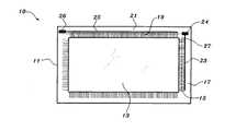
도 1은 종래의 TAB 실장 방식이 적용된 LCD 패널의 구조를 개략적으로 나타낸 평면도이다.1 is a plan view schematically showing a structure of an LCD panel to which a conventional TAB mounting method is applied.
도 1을 참조하면 TAB 실장 방식의 LCD 패널(10)은 TFT 소자가 형성된 TFT 기판(11)과, TFT 기판(11) 상부면에 부착되며 하부면에 칼라필터 패턴이 형성된 칼라필터 기판(13)으로 구성되어 있다.Referring to FIG. 1, the TAB
TFT 기판(11)의 세로 방향에는 복수개의 게이트 라인들(15)이 일렬로 배열된 게이트 영역(17)이 있고, TFT 기판(11)의 가로 방향에는 복수개의 데이터 라인들(19)이 일렬로 배열된 데이터 영역(21)이 있다. 여기서, 각각의 게이트 라인들(15) 및 데이터 라인들(19) 끝단에는 그로스 테스트시 게이트 라인(15) 및 데이터 라인(19)에 전압을 인가하기 위한 게이트 콘택 라인(23) 및 데이터 콘택 라인(25)이 연결되어 있으며, 게이트 및 데이터 콘택 라인(23)(25) 단부에는 프로브(미도시)가 접촉되는 게이트 핀 콘택부(24)와 데이터 핀 콘택부(26)가 형성되어 있다.In the longitudinal direction of the
이와 같이 구성된 LCD 패널의 그로브 테스트 과정을 설명하면 다음과 같다.Referring to the groove test process of the LCD panel configured as described above are as follows.
먼저, 게이트 핀 콘택부(24)와 데이터 핀 콘택부(26)에 프로브를 접촉시켜 게이트 콘택 라인(23)과 데이터 콘택 라인(25)에 각각에 전원을 인가한다. 이와 같이, 게이트 콘택 라인(23)과 데이터 콘택 라인(25)에 전압이 인가되면 게이트 콘택 라인(23)과 데이터 콘택 라인(25)에 공통적으로 연결되어 있는 각각의 게이트 및 데이터 라인(15)(19)에 전류가 흐르게 된다.First, a probe is contacted with the gate
이때, 테스트하고자 하는 LCD 패널이 예를 들어, 노말 화이트(normal white) 상태의 LCD 패널이면 전류가 인가 되었을 때에 블랙(black)으로 변하고, 테스트하고자 하는 LCD 패널이 예를 들어, 노말 블랙 상태의 패널인 경우 화이트 상태로 디스플레이된다. 만약, 게이트 라인(15) 또는 데이터 라인(19)의 불량으로 인해 전압이 인가되지 않을 경우 전압이 인가되지 않는 부분만이 화이트 상태, 또는 블랙 상태로 존재하게 되므로 LCD 패널의 불량 유무를 쉽게 확인할 수 있다.At this time, if the LCD panel to be tested is, for example, an LCD panel in a normal white state, it turns black when a current is applied, and the LCD panel to be tested is, for example, a panel in a normal black state. Is displayed in the white state. If a voltage is not applied due to a failure of the
이와 같이, 그로스 테스트가 완료되면 게이트 및 데이터 영역(17)(21)에 TAB IC를 본딩하기 위해서 게이트 및 데이터 콘택 라인(23)(25)을 절단하는데, 절단 방법은 TFT 기판(11)을 절단하는 유리 절단 방법과, 게이트 라인(15)과 데이터 라인(19)만을 절단하는 레이저 절단 방법이 있다. 여기서, 유리 절단 방법은 도 1에 도시된 바와 같이 콘택 라인 안쪽에 형성되어 있는 절단선(27)을 따라 게이트 영역(17)과 데이터 영역(21)의 유리를 절단하는 것으로 유리 절단시 유리 가루에 의해서 LCD 패널이 오염될 수 있는 문제점이 있다. 또한, 레이저 절단 방법은 레이저 빔을 이용하여 각각의 게이트 라인(15) 및 데이터 라인(19)만을 절단하는 방법으로 유리 절단 방법에 비해 제조 원가가 상승된다는 문제점이 있다.As such, when the gross test is completed, the gate and
이와 같이 핀 콘택 방법을 이용하여 그로스 테스트를 할 경우 그로스 테스트 후 게이트 및 데이터 콘택 라인(23)(25)을 절단하는 절단 공정이 추가됨으로써 LCD 패널의 수율이 저하되고, LCD 패널의 생산비용이 증가된다는 단점이 있다.As such, when the gross test is performed using the pin contact method, a cutting process for cutting the gate and
도 2 및 도 3을 참조하여 도전성 러버 콘택 방법을 이용한 그로스 테스트 방법을 설명하면 다음과 같다.The gross test method using the conductive rubber contact method will be described with reference to FIGS. 2 and 3 as follows.
도 2는 종래의 COG 방식의 LCD 패널을 개략적으로 나타낸 평면도이다.2 is a plan view schematically showing a conventional COG type LCD panel.
도 2를 참조하면, COG 방식의 LCD 패널(30)은 TFT 소자가 형성된 TFT 기판(31)과, TFT 기판(31) 상부면에 부착되며 하부면에 칼라필터 패턴이 형성된 칼라필터 기판(33)으로 구성되어 있다.Referring to FIG. 2, the COG
TFT 기판(31)의 세로 방향에는 게이트 영역(35)이 형성되어 있고, 게이트 영역(35) 위에는 게이트 구동 드라이브 IC를 본딩하기 위한 복수개의 게이트 라인들(39)이 "ㄷ"자 형상으로 형성되어 있다. 또한, TFT 기판(31)의 가로 방향에는 데이터 영역(37)이 형성되어 있으며, 데이터 영역(37) 위에는 데이터 구동 드라이브 IC를 본딩하기 위한 복수개의 데이터 라인들(41)이 "ㄷ"자 형상으로 형성되어 있다. 여기서, 각각의 게이트 라인(39) 및 데이터 라인(41) 말단에는 반도체 칩이 본딩되는 본딩 패드들(43)이 형성되어 있다.A
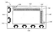
이와 같이 구성된 COG 방식의 LCD 패널을 테스트하기 위해서는 도 3에 도시된 바와 같은 테스트 장치가 이용된다. 도 3은 종래의 도전성 러버 콘택 방식에 적용되는 그로스 테스트 장치를 개략적으로 나타낸 사시도이다.In order to test the COG type LCD panel configured as described above, a test apparatus as shown in FIG. 3 is used. 3 is a perspective view schematically illustrating a gross test apparatus applied to a conventional conductive rubber contact method.
도 3에 도시된 바와 같이, 그로스 테스트 장치(50)는 소정의 리세스부(58)를 갖는 베이스 플레이트(51)가 있고, 베이스 플레이트(51)의 리세스부(58) 상부면 각 변에는 LCD 패널(30)을 수용하여 테스트하기 위한 인쇄회로 기판들(53)이 소정 높이로 돌출되어 있으며, 각각의 인쇄회로 기판들(53) 가장자리에는 LCD 패널(30)이 인쇄회로 기판들(53)에서 이탈되는 것을 방지하기 위한 턱부(55)가 형성되어 있다.As shown in FIG. 3, the
또한, LCD 패널(30)의 게이트 영역(35)과 데이터 영역(37)이 접촉되는 인쇄회로 기판들(53) 상부면에는 도전성 고무(57)가 부착되어 있는데, 그 위치는 게이트 라인(39) 및 데이터 라인들(41)이 "ㄷ" 형상을 이루고 있는 부분이며, 각각의 인쇄회로 기판들(53)에는 도전성 고무(57)에 전원을 인가하기 위한 전선(59)이 설치되어 있다.In addition, a
또한, 베이스 플레이트(51) 일측면에는 그로스 테스트시 베이스 플레이트(51) 전면을 덮도록 커버(63)가 힌지되어 있고, 커버(63) 하부면에는 각각의 인쇄회로 기판들(53)에 대응되도록 사각형상의 가압부(65)가 돌출되어 있다.In addition, the
이와 같이 구성된 LCD 패널의 그로스 테스트 방법을 설명하면 다음과 같다.The gross test method of the LCD panel configured as described above is as follows.
먼저, 테스트할 LCD 패널(30)을 인쇄회로 기판들(53) 상부면에 올려놓는데, 이때, LCD 패널(30)의 게이트 라인(39) 및 데이터 라인(41)은 인쇄회로 기판들(53) 상부면에 부착된 도전성 고무(57)와 접촉된다.First, the
이후, 일측이 힌지고정된 커버(63)로 베이스 플레이트(51) 전면을 덮게 되면 커버(63)로부터 돌출 형성된 가압부(65)는 LCD 패널(30)을 가압하여 복수개의 게이트 라인(39)들과 데이터 라인(41)들을 도전성 고무(57)에 밀착시킨다.Subsequently, when one side covers the front surface of the
이어서, 도전성 고무(57)에 전압을 인가하면 도전성 고무(57)에 첨가되어 있는 도전성 입자들(미도시)에 전압이 인가되고 도전성 입자들과 접촉되어 있는 각각의 게이트 라인(39) 및 데이터 라인들(41)은 도전성 입자에 의해서 전압이 공급된다. 이때, 테스트하고자 하는 LCD 패널이 예를 들어, 노말 화이트 상태의 LCD 패널인 경우 전압이 인가되면 블랙 상태로 디스플레이되지만, 복수개의 게이트 라인(39) 또는 데이터 라인들(41)중 어느 한 라인이 불량이면 그 라인에만 전압이 인가되지 않으므로 그 부분만이 화이트 상태로 존재하게 되어 LCD 패널 불량 유무를 확인할 수 있다.Subsequently, when a voltage is applied to the
그러나, 이와 같은 도전성 러버 콘택 방법을 이용하여 고해상도를 요구하는 LCD 패널을 테스트 할 경우 복수개의 데이터 라인(39) 및 데이터 라인들(41) 중 한 개의 라인 혹은 복수개의 라인이 도전성 고무(57)에 포함되어 있는 도전 입자와 접촉되지 않아 LCD 패널이 불량으로 판정되는 경우가 종종 발생되었다. 이는, 고해상도를 요구하는 LCD 패널의 경우 게이트 및 데이터 라인(39)(41)의 수가 많아 라인과 라인 사이의 간격이 좁은 반면에 도전성 고무(57)에 포함되어 있는 도전 입자와 입자 사이의 간격, 또는, 도전성 고무(57)에 포함되는 도전성 입자의 수에는 한계가 있으므로 도전 입자가 존재하지 않은 부분에 게이트 라인(39) 또는 데이터 라인(41)이 위치할 수 있다.However, when testing an LCD panel requiring high resolution using the conductive rubber contact method, one or more lines of the plurality of
이 경우 그 라인에만 전압이 인가되지 않기 때문에 LCD 패널의 초기상태인 노말 화이트 또는 노말 블랙 상태로 존재함으로 LCD 패널이 불량으로 판정되는 문제점이 있었다.In this case, since the voltage is not applied only to the line, the LCD panel is determined to be defective because the LCD panel is present in a normal white or normal black state.
따라서, 본 발명의 목적은 TAB 방식이 적용된 LCD 패널의 경우 그로스 테스트 후 콘택 라인을 절단하는 공정으로 인해 LCD 패널이 오염되거나, COG 방식의 LCD 패널의 경우 그로스 테스트시 게이트 라인 및 데이터 라인 접촉불량으로 인해 LCD 패널이 불량으로 판정되는 것을 방지하기 위해서 게이트 라인 및 데이터 라인 단부에 그로스 테스트용 TFT 소자를 형성하여 LCD 패널의 수율을 향상시키고 제조 코스트를 절감시킨 그로스 테스트용 TFT 소자 제조 방법 및 이를 형성한 액정 표시 장치 구조와 그로스 테스트 장치 및 방법을 제공하는데 있다.Therefore, an object of the present invention is to contaminate the LCD panel due to the process of cutting the contact line after the gross test in the case of the LCD panel to which the TAB method is applied, or the poor gate line and data line contact during the gross test in the case of the COG type LCD panel. In order to prevent the LCD panel from being judged to be defective, a gross test TFT device is formed at the gate line and data line ends, thereby improving the yield of the LCD panel and reducing the manufacturing cost. The present invention provides a liquid crystal display device and a gross test device and method.
도 1은 종래의 TAB 방식이 적용된 LCD 패널의 구조를 개략적으로 나타낸 평면도이다.1 is a plan view schematically showing the structure of an LCD panel to which a conventional TAB method is applied.
도 2는 종래의 COG 방식의 LCD 패널의 구조를 개략적으로 나타낸 평면도이다.2 is a plan view schematically showing the structure of a conventional COG type LCD panel.
도 3은 종래의 도전성 러버 콘택 방식에 적용되는 그로스 테스트 장치를 개략적으로 나타낸 사시도이다.3 is a perspective view schematically illustrating a gross test apparatus applied to a conventional conductive rubber contact method.
도 4a는 본 발명에 의한 COG 방식의 LCD 패널의 구조를 개략적으로 나타낸 평면도이고,4A is a plan view schematically showing the structure of a COG type LCD panel according to the present invention;
도 4b는 게이트 영역에 적용된 그로스 테스트용 TFT 소자를 개략적으로 도시한 평면도이고,4B is a plan view schematically showing a TFT device for gross test applied to a gate region,
도 4c는 게이트 영역에 적용된 그로스 테스트용 TFT 소자를 c-c´선으로 절단한 단면도이고,4C is a cross-sectional view taken along line c-c ′ of a TFT device for gross test applied to a gate region,
도 4d는 데이터 영역에 적용된 그로스 테스트용 TFT 소자를 개략적으로 도시한 평면도이고,FIG. 4D is a plan view schematically showing a TFT device for gross test applied to a data region,
도 4e는 데이터 영역에 적용된 그로스 테스트용 TFT 소자를 e-e´선으로 절단한 단면도이다.Fig. 4E is a cross sectional view of the gross test TFT element applied to the data area, cut along the line e-e '.
도 5는 본 발명에 의한 COG 방식의 또 다른 실시예를 개략적으로 나타낸 평면도이다.5 is a plan view schematically showing another embodiment of the COG method according to the present invention.
도 6a는 본 발명에 의한 LCD 패널의 그로스 테스트 장치를 개략적으로 나타낸 사시도이고,6A is a perspective view schematically illustrating a gross test apparatus of an LCD panel according to the present invention;
도 6b는 그로스 테스트 장치의 프로브에 게이트 핀 콘택부와 데이터 핀 콘택부가 접촉되는 상태를 나타낸 상태도이다.6B is a diagram illustrating a state in which a gate pin contact portion and a data pin contact portion contact a probe of a gross test apparatus.
도 7은 본 발명에 의한 TAB 방식의 LCD 패널의 구조를 개략적으로 나타낸 평면도이다.7 is a plan view schematically showing the structure of a TAB type LCD panel according to the present invention.
이와 같은 목적을 달성하기 위해서 TFT 기판 상부면에 금속을 증착하고 사진 식각하여 상기 TFT 기판의 게이트 영역에 게이트 라인 및 상기 게이트 라인과 소정 간격 이격된 그로스 테시트용 게이트 전극을 형성함과 아울러 상기 TFT 기판의 데이터 영역에 그로스 테스트용 게이트 전극을 형성하는 단계와; 상기 게이트 영역 및 상게 데이터 영역에 형성된 상기 그로스 테스트용 게이트 전극 상부면에 SiNx 물질과 a-Si:H 물질과 n+a-Si:H 물질을 연속적으로 도포한 후 절연층을 형성하고 상기 a-Si:H 물질과 상기 n+a-Si:H 물질을 사진 식각하여 게이트 전극 윗부분에만 반도체층을 형성하는 단계와; 상기 반도체층 상부면에 금속을 도포하고 사진 식각하여 상기 게이트 영역에 소스/드레인 전극을 형성함과 아울러 상기 데이터 영역에 그로스 테스트용 소스/드레인 전극과 일체로 데이터 라인을 형성하는 단계와; 상기 그로스 테스트용 소스/드레인 전극 상부면에 보호층을 형성하는 단계와; 상기 게이트 영역에 형성된 보호층 상부면, 즉, 드레인 전극이 위치한 부분의 보호층에만 마스크를 이용하여 콘택 홀을 형성하고 상기 보호층 상부면에 금속물질을 도포하여 상기 게이트 라인과 상기 드레인 전극을 상기 금속물질로 연결하는 단계를 포함하는 것을 특징으로 한다.In order to achieve the above object, a metal is deposited on the upper surface of the TFT substrate and photo-etched to form a gate line and a gate electrode for groste sheet spaced apart from the gate line in the gate region of the TFT substrate. Forming a gate test gate electrode in a data region of the substrate; The SiNx material, the a-Si: H material, and the n+ a-Si: H material are successively coated on the upper surface of the gross test gate electrode formed in the gate area and the data area, and then an insulating layer is formed. Photo-etching the Si: H material and the n+ a-Si: H material to form a semiconductor layer only over the gate electrode; Forming a source / drain electrode in the gate region by coating a metal on the upper surface of the semiconductor layer and etching the photo, and forming a data line integrally with a source / drain electrode for a growth test in the data region; Forming a protective layer on an upper surface of the source / drain electrode for the growth test; A contact hole is formed using a mask only on the upper surface of the passivation layer formed in the gate region, that is, the portion where the drain electrode is located, and a metal material is coated on the passivation layer to form the gate line and the drain electrode. It characterized in that it comprises a step of connecting with a metal material.
바람직하게는 상기 콘택 홀에 채워지는 금속 물질은 ITO 금속인 것을 특징으로 한다.Preferably, the metal material filled in the contact hole is ITO metal.
또한, 상부면에 TFT 소자가 형성되어 있고 측면에 게이트 라인들 및 데이터 라인들이 형성된 게이트 영역 및 데이터 영역으로 으로 구성된 TFT 기판과, 상기 TFT 기판 상부면에 부착되며 하부면에 칼라 필터 패턴이 형성된 칼라 필터 기판을 포함하는 액정 표시 장치에 있어서, 상기 게이트 라인들 및 상기 데이터 라인들 단부를 따라 상기 액정 표시 장치의 픽셀 상태를 테스트하기 위한 그로스 테스트용 TFT 소자가 형성된 것을 특징으로 한다.In addition, a TFT substrate having a TFT element formed on an upper surface and having a gate area and a data area having gate lines and data lines formed on a side thereof, and a color attached to an upper surface of the TFT substrate and having a color filter pattern formed on a lower surface thereof. A liquid crystal display device comprising a filter substrate, characterized in that a gross test TFT element for testing a pixel state of the liquid crystal display device is formed along end portions of the gate lines and the data lines.
바람직하게는 상기 게이트 영역 및 데이터 영역에 상기 그로스 테스트용 TFT 소자를 형성하기 위해서 상기 게이트 라인 및 상기 데이터 라인을 소정 길이로 연장한 것을 특징으로 하며 상기 연장된 게이트 라인의 재질은 ITO 금속인 것을 특징으로 한다.Preferably, the gate line and the data line are extended to a predetermined length in order to form the gross test TFT device in the gate region and the data region, and the material of the extended gate line is ITO metal. It is done.
또한, 상기 그로스 테스트용 TFT 소자에 연결되어 있는 상기 게이트 라인 및 상기 데이터 라인은 그로스 테스트시 상기 그로스 테스트용 TFT 소자의 드레인 전극 역할을 하는 것을 특징으로 한다.In addition, the gate line and the data line connected to the gross test TFT device may serve as a drain electrode of the gross test TFT device during a gross test.
본 발명의 다른 특징은 테스트될 LCD 패널이 놓여지는 베이스 플레이트와, 상기 베이스 플레이트 상부면 가장자리를 따라 형성되어 상기 LCD 패널의 TFT 기판과 접촉되는 턱부와, 상기 LCD 패널의 칼라필터 기판을 수용하는 리세스부와, 상기 리세스부 상부면중 상기 LCD 패널의 게이트 영역과 데이터 영역에 대응되는 부분에 돌출 형성되어 있어 상기 LCD 패널에 전압을 인가하는 프로브를 포함하는 것을 특징으로 한다.Another feature of the present invention is to accommodate a base plate on which an LCD panel to be tested is placed, a jaw portion formed along an upper edge of the base plate and in contact with a TFT substrate of the LCD panel, and a color filter substrate of the LCD panel. And a probe which protrudes in a portion corresponding to a gate area and a data area of the LCD panel from an upper surface of the recess and an upper surface of the recess to apply a voltage to the LCD panel.
본 발명의 또 다른 특징은 테스트될 LCD 패널의 게이트 영역과 데이터 영역에 형성되어 있는 TFT 소자들이 프로브에 접촉되도록 상기 LCD 패널을 그로스 테스트 장치의 베이스 플레이트 턱부에 올려놓는 단계와, 상기 프로브에서 상기 그로스 테스트용 TFT 소자에 전압을 인가하여 상기 LCD 패널의 픽셀 상태를 테스트하는 단계를 포함하는 것을 특징으로 한다.Another feature of the invention is the step of placing the LCD panel on the base plate chin of the gross test apparatus so that the TFT elements formed in the gate area and the data area of the LCD panel to be tested are in contact with the probe, and the gross in the probe And testing the pixel state of the LCD panel by applying a voltage to a test TFT device.
이하 본 발명에 의한 그로스 테스트 방법 및 그로스 테스트 장치를 첨부된 도면 도 4 와 도 5 및 도 6 및 도 7을 참조하여 설명하면 다음과 같다.Hereinafter, a gross test method and a gross test apparatus according to the present invention will be described with reference to FIGS. 4 and 5 and 6 and 7.
도 4는 본 발명에 의한 COG 방식의 LCD 패널을 개략적으로 나타낸 평면도이다.4 is a plan view schematically showing an LCD panel of the COG method according to the present invention.
도시된 바와 같이 본 발명에 의한 COG 방식의 LCD 패널(100)은 TFT 소자가 형성된 TFT 기판(101)과, TFT 기판(101) 상부면에 부착되고 하부면에 칼라필터 패턴이 형성된 칼라필터 기판(103)으로 구성되어 있다.As illustrated, the COG
TFT 기판(101)의 세로 방향에는 게이트 영역(105)이 형성되어 있는데, 게이트 영역(105) 위에는 반도체 칩을 본딩하기 위한 게이트 라인들(111)이 "ㄷ"자 형상(110)으로 형성되어 있고, 각각의 게이트 라인들(111) 단부에는 본딩 패드(113)가 형성되어 있으며 본딩 패드(113)에서 게이트 라인(111´)이 소정 길이 연장되어 형성되어 있다. 여기서, 바람직하게 본딩 패드(113)까지의 게이트 라인(111)의 재질은 알루미늄 또는 크롬 등과 같은 금속재질이고, 본딩 패드(113)에서 연장된 부분의 게이트 라인(111´)의 재질은 ITO 금속인 것이 바람직하다.A
또한, TFT 기판(101) 가로 방향에는 데이터 영역(107)이 형성되어 있는데, 데이터 영역(107) 위에는 반도체 칩을 본딩하기 위한 데이터 라인들(121)이 "ㄷ"자 형상(120)으로 형성되어 있고, 각각의 데이터 라인들(121) 단부에는 본딩 패드들(123)이 형성되어 있으며 본딩 패드(123)에서 데이터 라인(121´)이 소정 길이 연장되어 있다. 여기서, 데이터 라인(121) 및 연장된 데이터 라인(121´)과 본딩패드들(123)은 동일한 금속 재질로 형성하는 것이 바람직하다.In addition, the
또한, 본딩 패드(123)에서 연장된 각각의 게이트 라인(111´) 및 데이터 라인들(121´) 단부는 게이트 전극(131), 절연층(132), 반도체층(133), 비정질 실리콘층(135), 소스/드레인 전극(136)(137), 보호층(138)으로 이루어진 그로스 테스트용 TFT 소자(130)와 연결되어 있다. 여기서, 그로스 테스트용 TFT 소자(130)는 픽셀용 TFT 소자(미도시)를 형성할 때 함께 형성되며, 그로스 테스트용 TFT 소자(130)에 접촉되는 각각의 게이트 라인(111´) 및 데이터 라인(121´)은 그로스 테스트시 드레인 전극 역할을 한다.In addition, ends of the
미설명 부호 131´는 게이트 전극의 소정영역에 형성되어 게이트 전극에 전압을 인가하는 게이트 핀 콘택부이고, 135´는 소스 전극의 소정영역에 형성되어 소스 전극에 전압을 인가하는 소스 핀 콘택부이다.Reference numeral 131 'is a gate pin contact portion formed in a predetermined region of the gate electrode to apply a voltage to the gate electrode, and 135' is a source pin contact portion formed in a predetermined region of the source electrode to apply a voltage to the source electrode. .
한편, 도 4에서 게이트 영역(105) 및 데이터 영역(107)에 형성된 게이트 라인들(111) 및 데이터 라인들(121)의 반도체 칩 실장 영역이 작을 경우, 도 5에 도시된 바와 같이 게이트 영역(141) 및 데이터 영역(142)과 각각의 대응하는 TFT 기판(141) 측면(144)(145)에 게이트 라인(146) 및 데이터 라인(147)을 일렬로 형성하고 그 단부에 그로스 테스트용 TFT 소자(130)를 형성할 수도 있다.Meanwhile, when the semiconductor chip mounting regions of the
이와 같이 구성된 본 발명에 의한 COG 방식의 LCD 패널을 테스트하기 위해서는 도 6에 도시된 것과 같은 테스트 장치가 이용된다. 도 6는 본 발명에 의한 LCD 패널의 그로스 테스트 장치를 개략적으로 나타낸 사시도이다.In order to test a COG type LCD panel according to the present invention configured as described above, a test apparatus as shown in FIG. 6 is used. Figure 6 is a perspective view schematically showing a gross test apparatus of the LCD panel according to the present invention.
본 발명에 따른 테스트 장치(150)는 LCD 패널(100)이 놓여지는 베이스 플레이트(151)와, 베이스 플레이트(151) 상부면 가장자리를 따라 형성되고 LCD 패널(100)이 베이스 플레이트(151)를 이탈하는 것을 방지하기 위한 턱부(153)와, LCD 패널(100)의 칼라필터 기판(103)을 수용하는 리세스부(154)와, 리세스부(154) 상부면중 LCD 패널(100)의 게이트 영역(105)과 데이터 영역(107)에 대응되는 부분에 돌출 형성되며 그로스 테스트용 TFT 소자의 게이트 핀 콘택부(131´)와 소스 핀 콘택부(135´)에 전압을 인가하는 프로브(155)로 구성되어 있다.The
여기서, 게이트 영역 및 데이터 영역에 형성되는 그로스 테스트용 TFT 소자의 제조 방법을 도 4를 참조하여 설명하면 다음과 같다. 그로스 테스트용 TFT 소자는 픽셀용 TFT 소자와 동시에 형성되지만 그로스 테스트 TFT 소자를 중심으로 설명한다.Here, a method of manufacturing a gross test TFT element formed in the gate region and the data region will be described with reference to FIG. 4. Although the gross test TFT element is formed simultaneously with the pixel TFT element, it demonstrates centering on a gross test TFT element.
먼저, TFT 기판(101) 전면에 게이트 전극을 위한 금속을 증착하고 마스크를 이용하여 증착된 금속을 사진 식각한다. 그러면, TFT 기판(101)의 게이트 영역(105)에 픽셀용 게이트 전극(미도시)에서 연장된 게이트 라인(111) 및 게이트 라인(111)에서 소정 간격 이격된 영역에 그로스 테스트용 게이트 전극(131)이 동시에 형성된다.First, a metal for the gate electrode is deposited on the
또한, 게이트 라인(111) 및 그로스 테스트용 게이트 전극(131)이 게이트 전극에 형성될 때 데이터 영역(107)에 그로스 테스트용 게이트 전극(131)이 동시에 형성된다.In addition, when the
이후, 게이트 영역(105) 및 데이터 영역(107)에 그로스 테스트용 게이트 전극(131)이 형성되면 그로스 테스트용 게이트 전극(131) 상부면에 절연층(132)을 형성하기 위해 SiNx 물질을 도포하고, SiNx 물질 상부면, 즉, 절연층(132) 상부면에 a-Si:H 물질과 n+a-Si:H 물질을 연속적으로 도포한다. 이후, 마스크를 이용해서 n+a-Si:H 물질만을 1차 사진 식각하여 그로스 테스트용 게이트 전극(131) 윗부분에만 n+a-Si:H 물질을 남긴다. 이와 같이, 그로스 테스트용 게이트 전극 윗부분에 남아 있는 n+a-Si:H 물질을 a-Si:H 물질에 대한 마스크로 이용하여 a-Si:H 물질을 사진 식각하고 현상하여 절연층(132) 상부면에 반도체층(133)을 형성한다.After that, when the gate
이후, 1차 현상된 n+a-Si:H 물질 상부면에 소스/드레인 전극(135)(136)을 위한 금속을 층착하고 마스크를 이용하여 증착된 금속을 사진 식각한다. 그러면, 게이트 영역(105)에 형성된 n+a-Si:H 물질 상부면에는 그로스 테스트용 소스/드레인 전극(135)(136)이 형성된다. 그리고, 데이터 영역(107) 상부면에는 픽셀용 소스/드레인 전극(미도시)에서 연장된 데이터 라인(121)이 형성되고, n+a-Si:H 물질 상부면에는 데이터 라인(121)과 일체로 연결된 그로스 테스트용 소스/드레인 전극(135)(136)이 형성된다. 여기서, 그로스 테스트용 소스/드레인 전극(135)(136)과 일체로 형성된 데이터 라인(121)은 그로스 테스트시 드레인 전극(136) 역할을 한다.Subsequently, the metal for the source /
이와 같이, 게이트 영역(105) 및 데이터 영역(107)에 그로스 테스트용 소스/드레인 전극(135)(136)이 형성되면 소스/드레인 전극(135)(136)을 마스크로 이용하여 n+a-Si:H 층을 2차 사진 식각하여 반도체층(133) 상부면에 비정질 실리콘층(134)을 현상한다.As such, when the gross test source /
계속해서, 게이트 영역(105) 및 데이터 영역(107)에 소스/드레인 전극(135)(136) 및 비정질 실리콘층(134)이 형성되면 그로스 테스트용 소스/드레인 전극(135)(136) 상부면에 그로스 테스트용 TFT 소자(130)를 보호하기 위한 보호 물질을 도포하여 보호층(137)을 형성한다.Subsequently, when the source /
이후, 마지막 공정으로 게이트 영역(105)에 형성된 보호층(137)에만 마스크를 사용하여 콘택 홀(138)을 뚫는데, 콘택 홀(138)을 뚫는 위치는 드레인 전극(136)이 위치한 부분이다. 이어서, 사진 식각에 의해 보호층(137) 상부면에서 드레인 전극(136) 소정 영역까지 콘택 홀(138)이 뚫어지면 보호층(137) 상부면에 ITO(Indium Tin Oxide)금속(139)을 도포한 후 사진 식각하여 ITO 금속(139)이 게이트 라인(111)과 연결되도록 하여 게이트 라인(139)이 그로스 테스트시 드레인 전극(136) 역할을 하도록 한다.Subsequently, as a final process, a hole is used to drill the
도 6에 도시된 그로스 테스트 장치를 이용하여 본 발명에 의한 LCD 패널의 그로스 테스트 과정을 설명하면 다음과 같다.Referring to the gross test process of the LCD panel according to the present invention using the gross test apparatus shown in FIG.
먼저, 테스트할 LCD 패널(100)의 게이트 영역(105)과 데이터 영역(107)이 리세스부(154)에 돌출된 프로브(155)에 접촉되도록 LCD 패널(100)을 베이스 플레이트(141) 상부면에 올려놓는다. 이를 좀더 상세히 언급하면, 도 6b에 도시된 바와 같이 게이트 영역(105) 및 데이터 영역(107)에 형성된 그로스 테스트용 TFT 소자(130)중 게이트 전극(131)에 형성된 게이트 핀 콘택부(131´)와 소스 전극(135)에 형성된 소스 핀 콘택부(135´)를 각각의 프로브(155a)(155b)에 접촉시킨다.First, the
이와 같이 게이트 핀 콘택부(131´)와 소스 핀 콘택부(135´)가 각각의 프로브(155a)(155b)에 접촉되면 LCD 패널(100)의 픽셀 상태를 테스트하기 위해 각각의 프로브(155a)(155b)에 전압을 인가한다. 이때, 소스 핀 콘택부(135´)에 인가된 전압은 반도체층(133)을 따라 드레인 전극(136)으로 흐르게 되고, 게이트 핀 콘택부(131´)에 인가된 전압은 소스 및 드레인 전극(135)(136)간에 흐르는 전류량을 제어함으로 게이트 라인(111) 및 데이터 라인(121)에 인가되는 전압을 조절하여 그로스 테스트시 필요한 전압을 공급한다. 또한, 그로스 테스트용 TFT 소자(130)에 연결되어 있는 모든 게이트 라인(111)과 데이터 라인(121)은 그로스 테스트시 TFT 소자(130)의 드레인 전극(136) 역할을 함으로써 모든 게이트 라인(111) 및 데이터 라인(121)에 전류를 전부 공급할 수 있다.As such, when the gate
이와 같이 모든 게이트 전극(111)과 데이터 라인(121)에 전류가 공급되면 테스트하고자 하는 LCD 패널, 예를 들어, 노말 화이트 상태의 LCD 패널일 경우 블랙상태로 디스플레이되며, 만약, 게이트 라인(111) 또는 데이터 라인(121) 불량으로 인해 전류가 흐르지 않을 경우 그 부분만이 화이트 상태로 남아 있어 LCD 패널의 불량 유무를 확인할 수 있다.As such, when current is supplied to all the
도 7은 본 발명에 의한 제 2 실시예에 의한 TAB 실장 방식의 LCD 패널을 개략적으로 나타낸 평면도이다.7 is a plan view schematically showing an LCD panel of a TAB mounting method according to a second embodiment of the present invention.
본 발명에 의한 TAB 실장 방식의 LCD 패널(160)은 TFT 소자가 형성된 TFT 기판(161)과, TFT 기판(161) 상부면에 부착되며 하부면에 칼라필터 패턴이 형성된 칼라필터 기판(163)으로 구성되어 있다.The
TFT 기판(161) 세로 방향에는 복수개의 게이트 라인들(169)이 일렬로 배열된 게이트 영역(167)이 있고, TFT 기판(161) 가로 방향에는 복수개의 데이터 라인(173)이 일렬로 배열된 데이터 영역(171)이 있다.In the vertical direction of the
또한, 각각의 게이트 라인(169) 및 데이터 라인(173) 끝단에는 게이트 전극, 절연층, 반도체층, 비정질 실리콘층, 소스/드레인 전극, 보호층으로 이루어진 그로스 테스트용 TFT 소자(130)와 연결되어 있다.In addition, each
여기서, TAB 방식이 적용된 LCD 패널의 그로스 테스트용 TFT 소자 제조 방법 및 그로스 테스트 장치의 구성과 테스트 과정은 상기에서 설명한 COG 방식의 LCD 패널의 그로스 테스트 TFT 소자 제조 방법, 그로스 테스트 장치 및 방법과 같은 원리이므로 상세한 설명은 생략하기로 한다.Here, the configuration and test procedure of the GSE test TFT device manufacturing method and the GOS test device of the LCD panel to which the TAB method is applied are the same principles as the Gross Test TFT device manufacturing method, the gross test device and the method of the COG method LCD panel described above. Therefore, detailed description will be omitted.
TAB 실장 방식의 LCD 패널(160)에 그로스 테스트용 TFT 소자(130)를 형성하면 그로스 테스트 후 TAB IC를 실장하기 위해서 게이트 라인(169) 및 데이터 라인(173)을 절단할 필요가 없으므로 LCD 패널이 유리 가루에 의해 오염될 우려가 없으며 LCD 패널의 생산비용이 절감된다.When the
이상에서 설명한 바와 같이 본 발명은 TFT 기판에 TFT 소자를 형성할 때 게이트 영역 및 데이터 영역에 그로스 테스트용 TFT 소자를 함께 형성하고 그로스 테스트시 게이트 라인 및 데이터 라인을 그로스 테스트용 TFT 소자의 드레인 전극으로 사용한다.As described above, according to the present invention, when forming a TFT device on a TFT substrate, a gross test TFT device is formed together in a gate region and a data area, and when the gross test is performed, the gate line and the data line are used as drain electrodes of the gross test TFT device. use.
따라서, TAB 방식의 LCD 패널의 경우 그로스 테스트 후 게이트 라인 및 데이터 라인을 절단하는 절단 공정이 제거되므로 LCD 패널의 수율을 향상시킬 수 있고 LCD 패널의 제작비용을 절감할 수 있는 효과가 있다.Therefore, in the case of the TAB type LCD panel, since the cutting process of cutting the gate line and the data line after the gross test is removed, the yield of the LCD panel can be improved and the manufacturing cost of the LCD panel can be reduced.
또한, 고해상도를 요구하는 COG 방식의 LCD 패널의 경우 게이트 라인과 데이터 라인 전부에 전원이 공급됨으로 게이트 라인 및 데이터 라인에 전원이 공급되지 않아 LCD 패널이 불량 판정되는 것을 방지할 수 있어 LCD 패널의 수율을 향상시킬 수 있는 효과가 있다.In addition, in the case of a COG type LCD panel requiring high resolution, power is supplied to both the gate line and the data line, thereby preventing the LCD panel from being judged poor because power is not supplied to the gate line and the data line. There is an effect to improve.
Claims (12)
Translated fromKoreanPriority Applications (2)
| Application Number | Priority Date | Filing Date | Title |
|---|---|---|---|
| KR1019970013389AKR100239749B1 (en) | 1997-04-11 | 1997-04-11 | Tft fabrication method structure of lcd, test apparatus and method for gross test |
| US08/957,229US6590624B1 (en) | 1997-04-11 | 1997-10-24 | LCD panels including interconnected test thin film transistors and methods of gross testing LCD panels |
Applications Claiming Priority (1)
| Application Number | Priority Date | Filing Date | Title |
|---|---|---|---|
| KR1019970013389AKR100239749B1 (en) | 1997-04-11 | 1997-04-11 | Tft fabrication method structure of lcd, test apparatus and method for gross test |
Publications (2)
| Publication Number | Publication Date |
|---|---|
| KR19980076609A KR19980076609A (en) | 1998-11-16 |
| KR100239749B1true KR100239749B1 (en) | 2000-01-15 |
Family
ID=19502540
Family Applications (1)
| Application Number | Title | Priority Date | Filing Date |
|---|---|---|---|
| KR1019970013389AExpired - Fee RelatedKR100239749B1 (en) | 1997-04-11 | 1997-04-11 | Tft fabrication method structure of lcd, test apparatus and method for gross test |
Country Status (2)
| Country | Link |
|---|---|
| US (1) | US6590624B1 (en) |
| KR (1) | KR100239749B1 (en) |
Cited By (5)
| Publication number | Priority date | Publication date | Assignee | Title |
|---|---|---|---|---|
| KR20040026007A (en)* | 2002-09-17 | 2004-03-27 | 삼성전자주식회사 | A gross tester of liquid crystal display panel |
| KR101069632B1 (en) | 2008-05-12 | 2011-10-04 | 베이징 비오이 옵토일렉트로닉스 테크놀로지 컴퍼니 리미티드 | Testing wiring structure and method for forming the same |
| KR101129440B1 (en)* | 2005-08-18 | 2012-03-27 | 삼성전자주식회사 | Display substrate and method for testing display panel having the same |
| KR101165473B1 (en) | 2005-12-30 | 2012-07-13 | 엘지디스플레이 주식회사 | LCD Panel and fabricating method thereof |
| WO2016188009A1 (en)* | 2015-05-28 | 2016-12-01 | 京东方科技集团股份有限公司 | Drive chip for driving display panel, display apparatus and drive control method |
Families Citing this family (24)
| Publication number | Priority date | Publication date | Assignee | Title |
|---|---|---|---|---|
| JP2001265248A (en)* | 2000-03-14 | 2001-09-28 | Internatl Business Mach Corp <Ibm> | Active matrix display device, and inspection method therefor |
| KR100596965B1 (en)* | 2000-03-17 | 2006-07-04 | 삼성전자주식회사 | Driving signal applying module, liquid crystal display panel assembly applying the same, and driving signal inspection method of the liquid crystal display panel assembly |
| US20020025100A1 (en)* | 2000-06-16 | 2002-02-28 | Mcgill University | Method and apparatus for OPTO-electronic built-in tests |
| TW539139U (en)* | 2001-04-03 | 2003-06-21 | Hannstar Display Corp | Automatic adhesion status checking machine for taping |
| KR100816336B1 (en)* | 2001-10-11 | 2008-03-24 | 삼성전자주식회사 | Thin film transistor substrate and its manufacturing method |
| KR100798320B1 (en)* | 2002-03-06 | 2008-01-28 | 엘지.필립스 엘시디 주식회사 | Inspection device and method of liquid crystal panel |
| KR100973803B1 (en)* | 2003-07-24 | 2010-08-03 | 삼성전자주식회사 | Liquid crystal display |
| KR100575233B1 (en)* | 2003-11-04 | 2006-05-02 | 엘지.필립스 엘시디 주식회사 | Liquid Crystal Display Manufacturing Method |
| US6940301B2 (en)* | 2003-12-12 | 2005-09-06 | Au Optronics Corporation | Test pad array for contact resistance measuring of ACF bonds on a liquid crystal display panel |
| TWI229199B (en)* | 2004-01-02 | 2005-03-11 | Au Optronics Corp | Testing apparatus of flat display |
| KR101051008B1 (en)* | 2004-08-24 | 2011-07-21 | 삼성전자주식회사 | Method for producing array substrate and array substrate produced thereby |
| TW200801755A (en)* | 2006-06-30 | 2008-01-01 | Innolux Display Corp | Thin film transistor substrate and liquid crystal display panel using the same |
| US8125237B2 (en)* | 2006-07-17 | 2012-02-28 | Scanimetrics Inc. | Thin film transistor array having test circuitry |
| KR100843148B1 (en)* | 2006-12-22 | 2008-07-02 | 삼성전자주식회사 | Liquid crystal display device, connector for test of liquid crystal display device and test method thereof |
| KR101076446B1 (en)* | 2007-04-13 | 2011-10-25 | 엘지디스플레이 주식회사 | Thin film transistor substrate and flat panel display comprising the same |
| JP4448535B2 (en)* | 2007-12-18 | 2010-04-14 | 株式会社 日立ディスプレイズ | Display device |
| KR101527971B1 (en)* | 2008-07-21 | 2015-06-10 | 삼성디스플레이 주식회사 | Organic electroluminescent display device |
| US9535273B2 (en)* | 2011-07-21 | 2017-01-03 | Photon Dynamics, Inc. | Apparatus for viewing through optical thin film color filters and their overlaps |
| CN102254502B (en)* | 2011-07-26 | 2013-03-27 | 深圳市华星光电技术有限公司 | Voltage test device and system for liquid crystal panel |
| KR102047005B1 (en)* | 2013-05-31 | 2019-11-21 | 삼성디스플레이 주식회사 | Organic Light Emitting Display Panel |
| CN104090391A (en)* | 2014-06-27 | 2014-10-08 | 京东方科技集团股份有限公司 | Array substrate and display device |
| US9797944B2 (en)* | 2014-11-10 | 2017-10-24 | Boe Technology Group Co., Ltd. | Test fixture and test method using the same |
| CN105609023B (en)* | 2015-12-31 | 2018-08-07 | 京东方科技集团股份有限公司 | A kind of testing element group, array substrate, detection device and detection method |
| US10698692B2 (en) | 2016-07-21 | 2020-06-30 | Advanced Micro Devices, Inc. | Controlling the operating speed of stages of an asynchronous pipeline |
Family Cites Families (3)
| Publication number | Priority date | Publication date | Assignee | Title |
|---|---|---|---|---|
| JP2792634B2 (en)* | 1991-06-28 | 1998-09-03 | シャープ株式会社 | Active matrix substrate inspection method |
| TW331599B (en)* | 1995-09-26 | 1998-05-11 | Toshiba Co Ltd | Array substrate for LCD and method of making same |
| TW329002B (en)* | 1996-06-05 | 1998-04-01 | Zenshin Test Co | Apparatus and method for inspecting a LCD substrate |
- 1997
- 1997-04-11KRKR1019970013389Apatent/KR100239749B1/ennot_activeExpired - Fee Related
- 1997-10-24USUS08/957,229patent/US6590624B1/ennot_activeExpired - Lifetime
Cited By (6)
| Publication number | Priority date | Publication date | Assignee | Title |
|---|---|---|---|---|
| KR20040026007A (en)* | 2002-09-17 | 2004-03-27 | 삼성전자주식회사 | A gross tester of liquid crystal display panel |
| KR101129440B1 (en)* | 2005-08-18 | 2012-03-27 | 삼성전자주식회사 | Display substrate and method for testing display panel having the same |
| KR101165473B1 (en) | 2005-12-30 | 2012-07-13 | 엘지디스플레이 주식회사 | LCD Panel and fabricating method thereof |
| KR101069632B1 (en) | 2008-05-12 | 2011-10-04 | 베이징 비오이 옵토일렉트로닉스 테크놀로지 컴퍼니 리미티드 | Testing wiring structure and method for forming the same |
| WO2016188009A1 (en)* | 2015-05-28 | 2016-12-01 | 京东方科技集团股份有限公司 | Drive chip for driving display panel, display apparatus and drive control method |
| US10304398B2 (en) | 2015-05-28 | 2019-05-28 | Boe Technology Group Co., Ltd. | Driver integrated circuit for driving display panel, display device and method for driving driver integrated circuit capable of providing different current intensities to different length transmission wires |
Also Published As
| Publication number | Publication date |
|---|---|
| US6590624B1 (en) | 2003-07-08 |
| KR19980076609A (en) | 1998-11-16 |
Similar Documents
| Publication | Publication Date | Title |
|---|---|---|
| KR100239749B1 (en) | Tft fabrication method structure of lcd, test apparatus and method for gross test | |
| EP0845697B1 (en) | Active matrix type liquid crystal display device resistant to static electricity | |
| US5541748A (en) | Liquid crystal display having patterned insulating and semiconductor layers and a method of fabricating the same | |
| US7522225B2 (en) | Chip-on-glass array substrate of liquid crystal display device and method of fabricating the same | |
| KR100675630B1 (en) | Liquid crystal display panel and manufacturing method thereof | |
| US7042149B2 (en) | Circuit array substrate for display device | |
| KR100759965B1 (en) | Liquid crystal display | |
| KR20100048002A (en) | Liquid crystal display and method of manufacturing the same | |
| KR980010531A (en) | In the liquid crystal display device, | |
| KR20180027693A (en) | Display device | |
| CN100501539C (en) | Flat panel display and manufacturing method thereof | |
| US5748267A (en) | Common gate line layout method for liquid crystal display device with gate scanning driver circuit on a display substrate | |
| GB2350225A (en) | Active matrix LCD electrode substrate | |
| US6628364B2 (en) | Liquid crystal display device and fabricating method thereof | |
| KR20010030494A (en) | Liquid crystal display device and method for repairing breakage of circuit lines thereof | |
| JP2865323B2 (en) | Liquid crystal display | |
| KR101375852B1 (en) | Liquid crystal display device | |
| KR101102020B1 (en) | LCD panel and manufacturing method | |
| KR100675629B1 (en) | Liquid crystal display panel and manufacturing method thereof | |
| KR101032439B1 (en) | Thin film transistor array substrate and manufacturing method thereof | |
| KR100816335B1 (en) | Thin film transistor substrate and method for attaching driving integrated circuit using same | |
| KR101048983B1 (en) | Liquid crystal display device having a partially crystallized thin film transistor and manufacturing method thereof | |
| KR100843478B1 (en) | Line-on glass liquid crystal panel and manufacturing method thereof | |
| KR100480860B1 (en) | LCD Display | |
| KR100977220B1 (en) | COG method liquid crystal panel inspection method |
Legal Events
| Date | Code | Title | Description |
|---|---|---|---|
| A201 | Request for examination | ||
| PA0109 | Patent application | St.27 status event code:A-0-1-A10-A12-nap-PA0109 | |
| PA0201 | Request for examination | St.27 status event code:A-1-2-D10-D11-exm-PA0201 | |
| R17-X000 | Change to representative recorded | St.27 status event code:A-3-3-R10-R17-oth-X000 | |
| P11-X000 | Amendment of application requested | St.27 status event code:A-2-2-P10-P11-nap-X000 | |
| P13-X000 | Application amended | St.27 status event code:A-2-2-P10-P13-nap-X000 | |
| PG1501 | Laying open of application | St.27 status event code:A-1-1-Q10-Q12-nap-PG1501 | |
| R18-X000 | Changes to party contact information recorded | St.27 status event code:A-3-3-R10-R18-oth-X000 | |
| PN2301 | Change of applicant | St.27 status event code:A-3-3-R10-R13-asn-PN2301 St.27 status event code:A-3-3-R10-R11-asn-PN2301 | |
| E701 | Decision to grant or registration of patent right | ||
| PE0701 | Decision of registration | St.27 status event code:A-1-2-D10-D22-exm-PE0701 | |
| PN2301 | Change of applicant | St.27 status event code:A-3-3-R10-R13-asn-PN2301 St.27 status event code:A-3-3-R10-R11-asn-PN2301 | |
| GRNT | Written decision to grant | ||
| PR0701 | Registration of establishment | St.27 status event code:A-2-4-F10-F11-exm-PR0701 | |
| PR1002 | Payment of registration fee | St.27 status event code:A-2-2-U10-U11-oth-PR1002 Fee payment year number:1 | |
| PG1601 | Publication of registration | St.27 status event code:A-4-4-Q10-Q13-nap-PG1601 | |
| R18-X000 | Changes to party contact information recorded | St.27 status event code:A-5-5-R10-R18-oth-X000 | |
| PN2301 | Change of applicant | St.27 status event code:A-5-5-R10-R13-asn-PN2301 St.27 status event code:A-5-5-R10-R11-asn-PN2301 | |
| PR1001 | Payment of annual fee | St.27 status event code:A-4-4-U10-U11-oth-PR1001 Fee payment year number:4 | |
| R18-X000 | Changes to party contact information recorded | St.27 status event code:A-5-5-R10-R18-oth-X000 | |
| R18-X000 | Changes to party contact information recorded | St.27 status event code:A-5-5-R10-R18-oth-X000 | |
| PR1001 | Payment of annual fee | St.27 status event code:A-4-4-U10-U11-oth-PR1001 Fee payment year number:5 | |
| R18-X000 | Changes to party contact information recorded | St.27 status event code:A-5-5-R10-R18-oth-X000 | |
| PR1001 | Payment of annual fee | St.27 status event code:A-4-4-U10-U11-oth-PR1001 Fee payment year number:6 | |
| PN2301 | Change of applicant | St.27 status event code:A-5-5-R10-R13-asn-PN2301 St.27 status event code:A-5-5-R10-R11-asn-PN2301 | |
| PN2301 | Change of applicant | St.27 status event code:A-5-5-R10-R13-asn-PN2301 St.27 status event code:A-5-5-R10-R11-asn-PN2301 | |
| PR1001 | Payment of annual fee | St.27 status event code:A-4-4-U10-U11-oth-PR1001 Fee payment year number:7 | |
| PR1001 | Payment of annual fee | St.27 status event code:A-4-4-U10-U11-oth-PR1001 Fee payment year number:8 | |
| PR1001 | Payment of annual fee | St.27 status event code:A-4-4-U10-U11-oth-PR1001 Fee payment year number:9 | |
| PR1001 | Payment of annual fee | St.27 status event code:A-4-4-U10-U11-oth-PR1001 Fee payment year number:10 | |
| PR1001 | Payment of annual fee | St.27 status event code:A-4-4-U10-U11-oth-PR1001 Fee payment year number:11 | |
| PR1001 | Payment of annual fee | St.27 status event code:A-4-4-U10-U11-oth-PR1001 Fee payment year number:12 | |
| PR1001 | Payment of annual fee | St.27 status event code:A-4-4-U10-U11-oth-PR1001 Fee payment year number:13 | |
| R18-X000 | Changes to party contact information recorded | St.27 status event code:A-5-5-R10-R18-oth-X000 | |
| PN2301 | Change of applicant | St.27 status event code:A-5-5-R10-R11-asn-PN2301 | |
| FPAY | Annual fee payment | Payment date:20121015 Year of fee payment:14 | |
| PR1001 | Payment of annual fee | St.27 status event code:A-4-4-U10-U11-oth-PR1001 Fee payment year number:14 | |
| PN2301 | Change of applicant | St.27 status event code:A-5-5-R10-R11-asn-PN2301 | |
| PN2301 | Change of applicant | St.27 status event code:A-5-5-R10-R14-asn-PN2301 | |
| FPAY | Annual fee payment | Payment date:20130930 Year of fee payment:15 | |
| PR1001 | Payment of annual fee | St.27 status event code:A-4-4-U10-U11-oth-PR1001 Fee payment year number:15 | |
| FPAY | Annual fee payment | Payment date:20141001 Year of fee payment:16 | |
| PR1001 | Payment of annual fee | St.27 status event code:A-4-4-U10-U11-oth-PR1001 Fee payment year number:16 | |
| R18-X000 | Changes to party contact information recorded | St.27 status event code:A-5-5-R10-R18-oth-X000 | |
| FPAY | Annual fee payment | Payment date:20150930 Year of fee payment:17 | |
| PR1001 | Payment of annual fee | St.27 status event code:A-4-4-U10-U11-oth-PR1001 Fee payment year number:17 | |
| PC1903 | Unpaid annual fee | St.27 status event code:A-4-4-U10-U13-oth-PC1903 Not in force date:20161022 Payment event data comment text:Termination Category : DEFAULT_OF_REGISTRATION_FEE | |
| PC1903 | Unpaid annual fee | St.27 status event code:N-4-6-H10-H13-oth-PC1903 Ip right cessation event data comment text:Termination Category : DEFAULT_OF_REGISTRATION_FEE Not in force date:20161022 |