KR100236671B1 - Vertically mounted semiconductor chip package having a printed circuit board and a heat sink and a package module including the same - Google Patents
Vertically mounted semiconductor chip package having a printed circuit board and a heat sink and a package module including the sameDownload PDFInfo
- Publication number
- KR100236671B1 KR100236671B1KR1019970046367AKR19970046367AKR100236671B1KR 100236671 B1KR100236671 B1KR 100236671B1KR 1019970046367 AKR1019970046367 AKR 1019970046367AKR 19970046367 AKR19970046367 AKR 19970046367AKR 100236671 B1KR100236671 B1KR 100236671B1
- Authority
- KR
- South Korea
- Prior art keywords
- circuit board
- semiconductor chip
- package
- printed circuit
- chip
- Prior art date
- Legal status (The legal status is an assumption and is not a legal conclusion. Google has not performed a legal analysis and makes no representation as to the accuracy of the status listed.)
- Expired - Fee Related
Links
Images


Classifications
- H—ELECTRICITY
- H05—ELECTRIC TECHNIQUES NOT OTHERWISE PROVIDED FOR
- H05K—PRINTED CIRCUITS; CASINGS OR CONSTRUCTIONAL DETAILS OF ELECTRIC APPARATUS; MANUFACTURE OF ASSEMBLAGES OF ELECTRICAL COMPONENTS
- H05K7/00—Constructional details common to different types of electric apparatus
- H05K7/20—Modifications to facilitate cooling, ventilating, or heating
- H—ELECTRICITY
- H01—ELECTRIC ELEMENTS
- H01L—SEMICONDUCTOR DEVICES NOT COVERED BY CLASS H10
- H01L23/00—Details of semiconductor or other solid state devices
- H01L23/34—Arrangements for cooling, heating, ventilating or temperature compensation ; Temperature sensing arrangements
- H01L23/36—Selection of materials, or shaping, to facilitate cooling or heating, e.g. heatsinks
- H—ELECTRICITY
- H01—ELECTRIC ELEMENTS
- H01L—SEMICONDUCTOR DEVICES NOT COVERED BY CLASS H10
- H01L23/00—Details of semiconductor or other solid state devices
- H01L23/12—Mountings, e.g. non-detachable insulating substrates
- H01L23/13—Mountings, e.g. non-detachable insulating substrates characterised by the shape
- H—ELECTRICITY
- H01—ELECTRIC ELEMENTS
- H01L—SEMICONDUCTOR DEVICES NOT COVERED BY CLASS H10
- H01L25/00—Assemblies consisting of a plurality of semiconductor or other solid state devices
- H01L25/03—Assemblies consisting of a plurality of semiconductor or other solid state devices all the devices being of a type provided for in a single subclass of subclasses H10B, H10D, H10F, H10H, H10K or H10N, e.g. assemblies of rectifier diodes
- H01L25/10—Assemblies consisting of a plurality of semiconductor or other solid state devices all the devices being of a type provided for in a single subclass of subclasses H10B, H10D, H10F, H10H, H10K or H10N, e.g. assemblies of rectifier diodes the devices having separate containers
- H01L25/105—Assemblies consisting of a plurality of semiconductor or other solid state devices all the devices being of a type provided for in a single subclass of subclasses H10B, H10D, H10F, H10H, H10K or H10N, e.g. assemblies of rectifier diodes the devices having separate containers the devices being integrated devices of class H10
- H—ELECTRICITY
- H01—ELECTRIC ELEMENTS
- H01L—SEMICONDUCTOR DEVICES NOT COVERED BY CLASS H10
- H01L2224/00—Indexing scheme for arrangements for connecting or disconnecting semiconductor or solid-state bodies and methods related thereto as covered by H01L24/00
- H01L2224/01—Means for bonding being attached to, or being formed on, the surface to be connected, e.g. chip-to-package, die-attach, "first-level" interconnects; Manufacturing methods related thereto
- H01L2224/42—Wire connectors; Manufacturing methods related thereto
- H01L2224/47—Structure, shape, material or disposition of the wire connectors after the connecting process
- H01L2224/48—Structure, shape, material or disposition of the wire connectors after the connecting process of an individual wire connector
- H01L2224/481—Disposition
- H01L2224/48151—Connecting between a semiconductor or solid-state body and an item not being a semiconductor or solid-state body, e.g. chip-to-substrate, chip-to-passive
- H01L2224/48221—Connecting between a semiconductor or solid-state body and an item not being a semiconductor or solid-state body, e.g. chip-to-substrate, chip-to-passive the body and the item being stacked
- H01L2224/48225—Connecting between a semiconductor or solid-state body and an item not being a semiconductor or solid-state body, e.g. chip-to-substrate, chip-to-passive the body and the item being stacked the item being non-metallic, e.g. insulating substrate with or without metallisation
- H01L2224/48227—Connecting between a semiconductor or solid-state body and an item not being a semiconductor or solid-state body, e.g. chip-to-substrate, chip-to-passive the body and the item being stacked the item being non-metallic, e.g. insulating substrate with or without metallisation connecting the wire to a bond pad of the item
- H—ELECTRICITY
- H01—ELECTRIC ELEMENTS
- H01L—SEMICONDUCTOR DEVICES NOT COVERED BY CLASS H10
- H01L2225/00—Details relating to assemblies covered by the group H01L25/00 but not provided for in its subgroups
- H01L2225/03—All the devices being of a type provided for in the same main group of the same subclass of class H10, e.g. assemblies of rectifier diodes
- H01L2225/10—All the devices being of a type provided for in the same main group of the same subclass of class H10, e.g. assemblies of rectifier diodes the devices having separate containers
- H01L2225/1005—All the devices being of a type provided for in the same main group of the same subclass of class H10, e.g. assemblies of rectifier diodes the devices having separate containers the devices being integrated devices of class H10
- H01L2225/1011—All the devices being of a type provided for in the same main group of the same subclass of class H10, e.g. assemblies of rectifier diodes the devices having separate containers the devices being integrated devices of class H10 the containers being in a stacked arrangement
- H01L2225/1017—All the devices being of a type provided for in the same main group of the same subclass of class H10, e.g. assemblies of rectifier diodes the devices having separate containers the devices being integrated devices of class H10 the containers being in a stacked arrangement the lowermost container comprising a device support
- H01L2225/1023—All the devices being of a type provided for in the same main group of the same subclass of class H10, e.g. assemblies of rectifier diodes the devices having separate containers the devices being integrated devices of class H10 the containers being in a stacked arrangement the lowermost container comprising a device support the support being an insulating substrate
- H—ELECTRICITY
- H01—ELECTRIC ELEMENTS
- H01L—SEMICONDUCTOR DEVICES NOT COVERED BY CLASS H10
- H01L2225/00—Details relating to assemblies covered by the group H01L25/00 but not provided for in its subgroups
- H01L2225/03—All the devices being of a type provided for in the same main group of the same subclass of class H10, e.g. assemblies of rectifier diodes
- H01L2225/10—All the devices being of a type provided for in the same main group of the same subclass of class H10, e.g. assemblies of rectifier diodes the devices having separate containers
- H01L2225/1005—All the devices being of a type provided for in the same main group of the same subclass of class H10, e.g. assemblies of rectifier diodes the devices having separate containers the devices being integrated devices of class H10
- H01L2225/1011—All the devices being of a type provided for in the same main group of the same subclass of class H10, e.g. assemblies of rectifier diodes the devices having separate containers the devices being integrated devices of class H10 the containers being in a stacked arrangement
- H01L2225/1017—All the devices being of a type provided for in the same main group of the same subclass of class H10, e.g. assemblies of rectifier diodes the devices having separate containers the devices being integrated devices of class H10 the containers being in a stacked arrangement the lowermost container comprising a device support
- H01L2225/1035—All the devices being of a type provided for in the same main group of the same subclass of class H10, e.g. assemblies of rectifier diodes the devices having separate containers the devices being integrated devices of class H10 the containers being in a stacked arrangement the lowermost container comprising a device support the device being entirely enclosed by the support, e.g. high-density interconnect [HDI]
- H—ELECTRICITY
- H01—ELECTRIC ELEMENTS
- H01L—SEMICONDUCTOR DEVICES NOT COVERED BY CLASS H10
- H01L2225/00—Details relating to assemblies covered by the group H01L25/00 but not provided for in its subgroups
- H01L2225/03—All the devices being of a type provided for in the same main group of the same subclass of class H10, e.g. assemblies of rectifier diodes
- H01L2225/10—All the devices being of a type provided for in the same main group of the same subclass of class H10, e.g. assemblies of rectifier diodes the devices having separate containers
- H01L2225/1005—All the devices being of a type provided for in the same main group of the same subclass of class H10, e.g. assemblies of rectifier diodes the devices having separate containers the devices being integrated devices of class H10
- H01L2225/1011—All the devices being of a type provided for in the same main group of the same subclass of class H10, e.g. assemblies of rectifier diodes the devices having separate containers the devices being integrated devices of class H10 the containers being in a stacked arrangement
- H01L2225/1047—Details of electrical connections between containers
- H01L2225/107—Indirect electrical connections, e.g. via an interposer, a flexible substrate, using TAB
- H—ELECTRICITY
- H01—ELECTRIC ELEMENTS
- H01L—SEMICONDUCTOR DEVICES NOT COVERED BY CLASS H10
- H01L2225/00—Details relating to assemblies covered by the group H01L25/00 but not provided for in its subgroups
- H01L2225/03—All the devices being of a type provided for in the same main group of the same subclass of class H10, e.g. assemblies of rectifier diodes
- H01L2225/10—All the devices being of a type provided for in the same main group of the same subclass of class H10, e.g. assemblies of rectifier diodes the devices having separate containers
- H01L2225/1005—All the devices being of a type provided for in the same main group of the same subclass of class H10, e.g. assemblies of rectifier diodes the devices having separate containers the devices being integrated devices of class H10
- H01L2225/1011—All the devices being of a type provided for in the same main group of the same subclass of class H10, e.g. assemblies of rectifier diodes the devices having separate containers the devices being integrated devices of class H10 the containers being in a stacked arrangement
- H01L2225/1094—Thermal management, e.g. cooling
Landscapes
- Engineering & Computer Science (AREA)
- Microelectronics & Electronic Packaging (AREA)
- Power Engineering (AREA)
- Physics & Mathematics (AREA)
- Condensed Matter Physics & Semiconductors (AREA)
- General Physics & Mathematics (AREA)
- Computer Hardware Design (AREA)
- Chemical & Material Sciences (AREA)
- Materials Engineering (AREA)
- Thermal Sciences (AREA)
- Cooling Or The Like Of Semiconductors Or Solid State Devices (AREA)
- Structures Or Materials For Encapsulating Or Coating Semiconductor Devices Or Solid State Devices (AREA)
Abstract
Translated fromKoreanDescription
Translated fromKorean본 발명은 인쇄회로기판과 방열판을 구비하는 수직실장형 반도체 칩 패키지 및 그를 포함하는 패키지 모듈에 관한 것으로서, 보다 구체적으로는 반도체 칩을 직접 금속 방열판에 부착시키거나 여러 금속층을 포함하는 인쇄회로기판을 사용함으로써 보다 우수한 열 방출 효과를 얻기 위한 수직실장형 반도체 칩 패키지 및 그 패키지들을 모듈화하고 방열 장치를 부착하여 열 방출 효과를 배가시킨 패키지 모듈에 관한 것이다.The present invention relates to a vertically mounted semiconductor chip package having a printed circuit board and a heat sink and a package module including the same. More specifically, the present invention relates to a printed circuit board which directly attaches a semiconductor chip to a metal heat sink or includes a plurality of metal layers. The present invention relates to a vertically mounted semiconductor chip package for obtaining a better heat dissipation effect, and a package module in which the packages are modularized and a heat dissipation device is attached to double the heat dissipation effect.
전자기기에 있어서 데이터의 전송 속도 및 처리 속도의 증가로 인하여 전력 소비가 점점 더 커짐에 따라, 패키지(package)의 열 방출량이 증가하여 전자기기의 신뢰성이 저하되거나 수명 시간이 줄어들게 된다. 알려진 바에 의하면, 예를 들어 접합 온도가 10℃ 상승할 경우 소자의 동작 수명 시간은 반으로 줄어든다. 따라서, 고전력 패키지에 있어서의 열 방출 문제는 점점 더 중요한 문제가 되고 있다. 특히, 논리 칩(logic chip), 파워 트랜지스터(power transistor) 등의 비메모리 분야 뿐만 아니라, 데이터의 빠른 전송 속도를 필요로 하는 디램(DRAM), 에스램(SRAM) 등의 메모리 분야에서도 열적인 문제가 대두되고 있는 추세이다.As the power consumption becomes larger due to the increase in the transmission speed and the processing speed of data in the electronic device, the heat dissipation amount of the package increases, thereby reducing the reliability of the electronic device or reducing the life time. It is known that, for example, when the junction temperature rises by 10 ° C, the operating life time of the device is cut in half. Therefore, the problem of heat dissipation in high power packages is becoming more and more important. In particular, not only non-memory fields such as logic chips and power transistors, but also thermal areas such as DRAMs and SRAMs that require fast data transfer rates. Is on the rise.
특히, 일반 디램(DRAM)의 경우, 메모리 칩의 정보처리 속도가 중앙처리장치(CPU)의 정보처리 속도를 따라가지 못해 데이터 병목 현상이 발생한다. 중앙처리장치가 연산하는 동안 명령어와 데이터를 일시 저장하는 디램(DRAM)에 있어서, 저장용량 자체는 현재 64M급의 제품이 생산되는 등 엄청나게 커졌지만, 데이터를 주고 받는 속도는 고성능화 추세에 있는 중앙처리장치에 비해 크게 뒤떨어진다.In particular, in the case of general DRAM, a data bottleneck occurs because the information processing speed of the memory chip does not match the information processing speed of the CPU. In the DRAM that temporarily stores instructions and data during the operation of the central processing unit, the storage capacity itself has grown enormously, including the production of 64M-class products, but the speed of sending and receiving data is increasing. Significantly behind the device.
그런데 최근에 기존 디램(DRAM)의 데이터 병목 현상을 제거하여 데이터 전송 속도의 향상을 꾀한 새로운 메모리 소자인 램버스 디램(Rambus DRAM)이 개발되어 소개되고 있다. 이 소자는 미국의 반도체 회사인 램버스사(Rambus Inc.)가 처음 개발한 소자로서, 초고속 정보처리로 시스템의 고성능화, 고속화를 실현할 수 있으며, 동영상 및 3차원 그래픽 처리가 가능한 차세대 메모리이다.Recently, a new memory device, Rambus DRAM, has been developed to remove data bottlenecks of existing DRAMs and improve data transfer speeds. The device was first developed by Rambus Inc., a US semiconductor company, and is a next-generation memory that can realize high performance and high speed of the system with ultra-high speed information processing, and can process video and 3D graphics.
복잡한 신호 전송망을 병렬로 배치하여 단순화하는 이른바 '버스(bus)' 방식을 채택한 것으로 알려지고 있는 램버스 디램(Rambus DRAM)은, 그 특성상 칩의 입/출력 패드(I/O pad)가 칩 면의 한쪽 방향에 치우쳐 설계되기 때문에, 그에 대응되는 패키지의 리드(lead) 또는 핀(pin)도 한쪽 방향으로만 나와 있어야 한다. 이 램버스 디램(Rambus DRAM)의 패키지 형태로는 표면 수직실장형 패키지(SVP; surface vertical package)와 표면 수평실장형 패키지(SHP; surface horizontal package)가 있다.Rambus DRAM, which is known to adopt a so-called 'bus' method of simplifying complex signal transmission networks in parallel, has its I / O pads on the chip surface. Since the design is oriented in one direction, the corresponding lead or pin of the package must also come out in one direction only. Package types of the Rambus DRAM include a surface vertical package (SVP) and a surface horizontal package (SHP).
표면 수직실장형 패키지(SVP)는 패키지의 한쪽 측면으로 돌출된 리드(lead)가 패키지 바깥 부위에서 직각으로 구부러졌으며, 구부러진 앞부분이 모 기판(mother board)에 닿도록 세워져서 실장된다. 실장 점유 면적은 전형적인 표면실장형 패키지인 SOJ(small outline J-lead package)의 1/7, ZIP(zigzag in-line package)의 1/3 정도로 매우 작다. 이 표면 수직실장형 패키지(SVP)를 모 기판에 실장하는 방법으로는, 패키지 양단에 형성된 돌기를 기판의 구멍에 꽂는 방법과, 패키지 양단에 형성된 여분의 핀이 좌우로 갈라져 패키지를 지지하는 방법 등이 가능하다.The surface vertical mounting package (SVP) is mounted so that a lead protruding to one side of the package is bent at a right angle from the outside of the package, and the bent front part is mounted so as to contact the mother board. The footprint is as small as 1/7 of the typical small surface J-lead package (SOJ) and 1/3 of the zigzag in-line package (ZIP). The surface vertical mounting package (SVP) can be mounted on a mother board by inserting protrusions formed at both ends of the package into the holes of the board, and extra pins formed at both ends of the package are divided left and right to support the package. This is possible.
반면에, 표면 수평실장형 패키지(SHP)는 TSOP(thin small outline package)와 유사한 구조로서, 실제 기능을 갖는 한쪽편의 리드들 및 단지 실장을 위해 반대편에 형성된 여분의 핀들에 의해 기판에 실장된다. 실장 높이는 일반적으로 SVP 형태가 SHP 형태보다 높다.On the other hand, a surface horizontal mount package (SHP) is a structure similar to a thin small outline package (TSOP), which is mounted on a substrate by leads on one side having practical functions and extra pins formed on the opposite side for mounting only. The mounting height is generally higher in SVP form than in SHP form.
그런데, 16M 또는 18M 램버스 디램(Rambus DRAM)은 이상 설명한 바와 같이 리드 프레임을 사용하여 패키지될 수 있으나, 64M급 이상의 램버스 디램(Rambus DRAM)은 전기적 특성 때문에 다층의 회로배선이 형성된 인쇄회로기판에 탑재되어 패키지된다. 이 때 최대의 동작 전력은 2.0~2.1W 정도로서, 열 방출 문제가 대두된다.By the way, 16M or 18M Rambus DRAM can be packaged using a lead frame as described above, but more than 64M Rambus DRAM is mounted on a printed circuit board having a multi-layer circuit wiring because of the electrical characteristics Packaged. At this time, the maximum operating power is about 2.0 ~ 2.1W, a problem of heat dissipation.
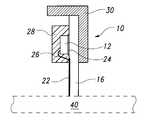
도 1과 그 단면도인 도 2에 인쇄회로기판(16)을 사용한 종래의 수직실장형 패키지(10)의 한 예를 보이고 있다. 도 1과 도 2를 참조하면, 구리 배선(22)이 형성되어 있는 인쇄회로기판(16) 표면에 반도체 칩(12)을 열전도성/전기절연성 접착제(24)로 부착시킨 후, 외부와의 전기적 연결을 위해 칩(12) 상면의 칩 패드(14)와 기판 패드(18)를 금속 세선(26)으로 연결한다. 기판 패드(18)는 구리 배선(22)을 통하여 기판 한쪽의 접속 패드(20)와 연결되며, 접속 패드(20)가 모 기판(40)에 삽입되어 접속된다. 칩(12)은 외부 환경으로부터 보호하기 위하여 봉지수지(28)를 사용하여 성형된다. 기판(16)의 반대쪽 면에는 방열판(30)이 부착된다.An example of a conventional vertically mounted
이와 같은 패키지(10)의 열 방출 경로는 다음과 같다. 칩(12) 상부면에서 발생한 고온의 열은 봉지수지(28), 기판(16) 및 방열판(30)을 통하여 패키지(10) 표면으로 전도되며, 패키지(10) 표면에 도달된 열은 대류 및 복사에 의하여 대기 중으로 방출된다. 도 3은 컴퓨터를 사용한 모의실험의 결과로서 온도 구배 분포를 보여주고 있다. 도 3에서 볼 수 있듯이, 봉지수지 및 수지 재질의 인쇄회로기판은 열전도성이 낮기 때문에, 칩에서 발생되는 열은 봉지수지 및 기판으로 둘러쌓이게 되어 효과적인 열 방출이 되지 않는다. 이러한 결과는 칩의 접합 온도를 상승시키게 되어, 데이터 처리 속도의 감소 및 사용상의 오동작, 전기적 특성의 불량들을 유발시키게 된다.The heat dissipation path of the
따라서, 본 발명의 목적은 효율적인 열 방출을 위하여 방열판을 포함하는 수직실장형 반도체 칩 패키지를 제공하는 데 있다.Accordingly, an object of the present invention is to provide a vertically mounted semiconductor chip package including a heat sink for efficient heat dissipation.
본 발명의 다른 목적은 전기적 특성의 향상을 위하여 인쇄회로기판을 포함하는 수직실장형 반도체 칩 패키지를 제공하는 데 있다.Another object of the present invention is to provide a vertically mounted semiconductor chip package including a printed circuit board to improve electrical characteristics.
본 발명의 또 다른 목적은 수직실장형 패키지가 수직으로 회로기판에 실장되고 상부에 방열 장치를 포함하는 패키지 모듈을 제공하는 데 있다.Still another object of the present invention is to provide a package module in which the vertically mounted package is mounted on a circuit board vertically and includes a heat dissipation device on the top.
본 발명의 또 다른 목적은 열 방출 특성과 전기적 특성이 우수한 램버스 디램 칩 패키지를 제공하는 데 있다.It is still another object of the present invention to provide a Rambus DRAM chip package having excellent heat dissipation characteristics and electrical characteristics.
도 1은 종래의 수직실장형 패키지의 한 예를 나타내는 평면도,1 is a plan view showing an example of a conventional vertical mounting package,
도 2는 도 1의 II-II선을 따라 절단한 단면도로서, 모 기판에 실장된 상태를 보여주는 도,FIG. 2 is a cross-sectional view taken along the line II-II of FIG. 1 and showing a state in which it is mounted on a mother substrate.
도 3은 도 1 및 도 2에 도시된 패키지의 온도 구배 분포를 보여주는 도,3 shows a temperature gradient distribution of the package shown in FIGS. 1 and 2;
도 4는 본 발명에 따른 수직실장형 패키지의 실시예를 나타내는 평면도,4 is a plan view showing an embodiment of a vertically mounted package according to the present invention;
도 5는 도 4의 V-V선을 따라 절단한 단면도로서, 패키지가 모 기판에 실장된 상태를 보여주는 도,FIG. 5 is a cross-sectional view taken along line V-V of FIG. 4, showing a state in which a package is mounted on a mother substrate.
도 6은 본 발명에 따른 수직실장형 패키지의 다른 실시예를 나타내는 평면도,6 is a plan view showing another embodiment of a vertically mounted package according to the present invention;
도 7은 도 6에 도시된 패키지의 저면도,7 is a bottom view of the package shown in FIG. 6, FIG.
도 8은 도 6의 VIII-VIII선을 따라 절단한 단면도로서, 패키지가 모 기판에 실장된 상태를 보여주는 도,FIG. 8 is a cross-sectional view taken along the line VIII-VIII of FIG. 6, showing a state in which a package is mounted on a mother substrate. FIG.
도 9는 본 발명에 따른 수직실장형 패키지의 또 다른 실시예를 나타내는 평면도,9 is a plan view showing another embodiment of a vertically mounted package according to the present invention;
도 10은 본 발명의 수직실장형 패키지를 포함하는 패키지 모듈의 실시예를 보여주는 도,10 is a view showing an embodiment of a package module including a vertically mounted package of the present invention;
도 11은 도 4 및 도 5에 도시된 수직실장형 패키지의 온도 구배 분포를 보여주는 도,11 is a view showing a temperature gradient distribution of the vertically mounted package shown in FIGS. 4 and 5;
도 12는 도 10에 도시된 패키지 모듈의 온도 구배 분포를 보여주는 도이다.FIG. 12 is a diagram illustrating a temperature gradient distribution of the package module illustrated in FIG. 10.
< 도면의 주요 부분에 대한 부호의 설명 ><Description of Symbols for Main Parts of Drawings>
10, 50, 80, 100 : 수직실장형 반도체 칩 패키지10, 50, 80, 100: vertically mounted semiconductor chip package
12, 52, 82, 102 : 반도체 칩 14, 54, 104 : 칩 패드12, 52, 82, 102:
16, 56, 84, 106 : 인쇄회로기판 18, 58, 108 : 기판 패드16, 56, 84, 106:
20, 60, 86, 110 : 접속 패드 22, 62, 88, 112 : 회로배선20, 60, 86, 110:
24, 64 : 접착층 26, 66, 116 : 금속 세선24, 64:
28, 68, 92, 118 : 봉지수지 30, 70, 94, 120 : 방열판28, 68, 92, 118:
40 : 모 기판 90 : 금속층40: mother substrate 90: metal layer
96 : 개재물질 130 : 패키지 모듈96: inclusion material 130: package module
132 : 방열 장치 134 : 제2 회로기판132: heat dissipation device 134: second circuit board
상기 목적을 달성하기 위하여, 본 발명은 인쇄회로기판과 방열판을 구비하는 수직실장형 반도체 칩 패키지를 제공한다. 본 발명의 수직실장형 패키지는 반도체 칩을 포함하며, 칩 상부면의 한쪽 가장자리에는 복수개의 칩 패드들이 형성된다. 금속 재질의 방열판은 칩의 하부면과 직접 접착되며, 인쇄회로기판은 칩의 외곽에 인접하여 형성된 복수개의 기판 패드들과, 기판 패드들과 회로배선을 통하여 각각 연결되며 외부 회로기판에 접속되기 위한 복수개의 접속 패드들을 포함한다. 칩 패드들과 기판 패드들은 각각 복수개의 금속 세선들에 의하여 전기적으로 연결되며, 반도체 칩과 금속 세선들과 기판 패드들은 봉지수지로 봉지된다.In order to achieve the above object, the present invention provides a vertically mounted semiconductor chip package having a printed circuit board and a heat sink. The vertically mounted package of the present invention includes a semiconductor chip, and a plurality of chip pads are formed at one edge of the upper surface of the chip. The heat sink made of metal is directly bonded to the lower surface of the chip, and the printed circuit board is connected to the plurality of substrate pads formed adjacent to the outer surface of the chip, and the substrate pads are connected to the external circuit boards through circuit wiring. It includes a plurality of connection pads. The chip pads and the substrate pads are electrically connected to each other by a plurality of fine metal wires, and the semiconductor chip, the fine metal wires and the substrate pads are encapsulated with an encapsulating resin.
본 발명의 수직실장형 반도체 칩 패키지는 램버스 디램(Rambus DRAM) 칩을 포함할 수 있으며, 특히 64M급 이상의 램버스 디램 칩을 적용할 경우에도 우수한 열 방출 특성과 전기적 특성을 나타낼 수 있다. 방열판의 크기는 칩의 크기보다 큰 것이 바람직하며, 이 때 인쇄회로기판은 칩의 외곽에 인접하여 방열판의 일부와 접착될 수 있다. 한편, 금속 세선은 금 세선이 바람직하며, 봉지수지는 에폭시 화합물이 바람직하다. 특히, 본 발명의 패키지는 2개 이상의 반도체 칩을 포함할 수 있다.The vertically mounted semiconductor chip package of the present invention may include a Rambus DRAM chip, and may exhibit excellent heat dissipation characteristics and electrical characteristics even when a Rambus DRAM chip of 64M or more is applied. The size of the heat sink is preferably larger than the size of the chip. In this case, the printed circuit board may be attached to a portion of the heat sink adjacent to the outside of the chip. On the other hand, the fine metal wire is preferably a gold fine wire, and the sealing resin is preferably an epoxy compound. In particular, the package of the present invention may include two or more semiconductor chips.
본 발명은 또한 상기 수직실장형 패키지들을 복수개 구비하는 패키지 모듈을 제공한다. 패키지 모듈은 제2 회로기판을 포함하며, 상기 패키지들이 각각의 인쇄회로기판을 통하여 제2 회로기판에 수직으로 실장되며, 인쇄회로기판의 접속 패드들을 통하여 제2 회로기판에 전기적으로 접속된다. 특히, 패키지 모듈은 각각의 방열판들과 접착되는 방열 장치를 더 포함할 수 있다.The present invention also provides a package module having a plurality of the vertically mounted packages. The package module includes a second circuit board, and the packages are mounted perpendicular to the second circuit board through each printed circuit board and electrically connected to the second circuit board through the connection pads of the printed circuit board. In particular, the package module may further include a heat dissipation device bonded to each of the heat sinks.
본 발명의 다른 면에 의하여 제공되는 수직실장형 반도체 칩 패키지는, 반도체 칩이 인쇄회로기판의 회로배선이 형성된 면에 직접 접착된다. 이 때 방열판은 인쇄회로기판의 접속 패드가 형성된 반대편에 끼워진다. 인쇄회로기판은 그 내부에 복수개의 접지 금속층을 포함할 수 있으며, 접지 금속층의 일부가 인쇄회로기판의 표면으로 노출되어 방열판과 접촉될 수 있다. 방열판과 접촉되는 접지 금속층의 노출 부위는 인쇄회로기판의 적어도 1개면 이상에 2개 이상 형성되는 것이 바람직하다. 그리고 방열판과 인쇄회로기판 사이에는 열전도성을 갖는 물질이 개재되는 것이 바람직하다. 상기 수직실장형 패키지들도 방열 장치를 포함하는 패키지 모듈로서 제공될 수 있다.In the vertically mounted semiconductor chip package provided by the other side of the present invention, the semiconductor chip is directly bonded to the side where the circuit wiring of the printed circuit board is formed. At this time, the heat sink is fitted to the opposite side on which the connection pad of the printed circuit board is formed. The printed circuit board may include a plurality of ground metal layers therein, and part of the ground metal layer may be exposed to the surface of the printed circuit board to be in contact with the heat sink. Preferably, at least two exposed portions of the ground metal layer in contact with the heat sink are formed on at least one surface of the printed circuit board. In addition, it is preferable that a material having thermal conductivity be interposed between the heat sink and the printed circuit board. The vertically mounted packages may also be provided as package modules including a heat dissipation device.
이하, 첨부 도면을 참조하여 본 발명의 실시예를 보다 상세하게 설명하고자 한다. 도면 전반을 통틀어 동일한 도면부호는 동일한 구성요소를 가리킨다.Hereinafter, with reference to the accompanying drawings will be described in detail an embodiment of the present invention. Like numbers refer to like elements throughout.
도 4는 본 발명에 따른 수직실장형 패키지(50)의 실시예를 나타내는 평면도이고, 도 5는 도 4의 V-V선을 따라 절단한 단면도로서, 패키지(50)가 모 기판(40)에 실장된 상태를 보여주는 도이다. 도 4와 도 5를 참조하면, 램버스 디램 칩(52)의 상부면의 한쪽 가장자리에 복수개의 칩 패드들(54)이 형성되어 있다. 칩(52)의 하부면은 얇은 접착층(64)을 통하여 직접 금속 방열판(70; heat spreader)에 부착된다. 따라서, 칩(52)에서 발생되는 열은 직접 금속 방열판(70)을 통하여 방열되기 때문에, 일단 봉지수지를 거쳐 방열되는 종래의 패키지보다 훨씬 우수한 방열 효과를 거둘 수 있다.4 is a plan view showing an embodiment of the vertically mounted
한편, 칩(54)보다 그 크기가 더 큰 방열판(70)을 사용함으로써, 인쇄회로기판(56)이 칩(52)의 외곽에 인접하여 방열판(70)의 일부와 접착될 수 있도록 한다. 따라서, 칩(52)에서 방열판(70)으로 전도되는 열은 인쇄회로기판(56)을 통해서도 방출될 수 있다. 이는 단지 봉지수지(68) 만을 통하여 인쇄회로기판(56)으로 열이 전달되는 것보다 훨씬 우수한 방열 효과를 나타낼 수 있다.On the other hand, by using a
인쇄회로기판(56)은 BT 수지, FR4, FR5 등의 재질로 이루어지며, 그 한쪽 면에 기판 패드들(58) 및 접속 패드들(60), 그리고 상기 패드들(58, 60)을 서로 이어주는 회로배선들(62)이 형성되어 있다. 기판 패드(58)는 칩(52)의 칩 패드(54)와 금속 세선(66)에 의하여 전기적으로 연결되는 곳이다. 따라서, 칩 패드(54)가 형성된 칩(52)의 가장자리에 최대한 근접하여 형성된다. 반면에, 접속 패드(60)는 패키지(50)가 모 기판(40, 또는 제2 회로기판)에 수직으로 실장될 때 전기적 접속 단자의 역할을 한다.The printed
도 4에 도시된 금속 세선(66)과 회로배선(62)은 복잡함을 피하기 위하여 그 일부만 도시되었으며, 이는 다음 실시예들의 참조 도면인 도 6과 도 9에서도 마찬가지이다. 기판 패드(58), 접속 패드(60) 및 회로배선(62)은 구리(Cu)로 이루어지며, 필요한 경우 도금 처리될 수 있다. 열전도성 및 전기전도도가 우수한 구리배선을 미세패턴으로 형성할 수 있는 인쇄회로기판(56)을 사용하기 때문에, 본 발명의 패키지(50)는 우수한 전기적 특성을 나타낼 수 있다.Only a part of the metal
금속 세선(66)은 금(Au) 세선이 주로 사용되며, 금속 세선(66) 및 칩(52), 기판 패드(58), 회로배선(62)의 일부는 에폭시 화합물(epoxy compound)과 같은 봉지수지(68)에 의하여 봉지된다. 방열판(70)은 칩(52)과 인쇄회로기판(56)의 하부쪽 뿐만 아니라, 패키지(50)가 모 기판(40)에 수직으로 실장되었을 때 모 기판(40)의 반대편, 즉 패키지(50)의 상부쪽으로도 연장되어 형성될 수 있다. 이는 열 방출 효과를 더 높여줄 뿐만 아니라, 추후에 설명할 모듈 제조 시에 다른 방열 장치를 추가로 부착할 수 있도록 해 준다.The metal
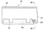
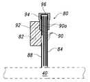
도 6과 도 7은 각각 본 발명에 따른 수직실장형 패키지(80)의 다른 실시예를 나타내는 평면도와 저면도이다. 그리고, 도 8은 도 6의 VIII-VIII선을 따라 절단한 단면도로서, 패키지(80)가 모 기판(40)에 실장된 상태를 보여주는 도이다. 도 6 내지 도 8에 도시된 바와 같이, 램버스 디램 칩(82)은 전술한 예와는 달리 인쇄회로기판(84)에 부착된다. 즉, 인쇄회로기판(84)은 칩(82)의 외곽에 있지 않고, 회로배선(88)이 형성된 면이 칩(82)의 하부면과 접착되도록 칩(82)의 하부쪽에 위치한다. 한편, 접속 패드(86)는 인쇄회로기판(84)의 상부면 뿐만 아니라(도 6 참조), 하부면에도 형성될 수 있다(도 7 참조).6 and 7 are a plan view and a bottom view, respectively, showing another embodiment of the vertically mounted
인쇄회로기판(84)은 열 방출 효과를 향상시키기 위하여 그 내부에 여러개의 접지 금속층(90)을 포함할 수 있다. 이 금속층(90)은 회로배선(88)이 형성된 부분을 제외하고 인쇄회로기판(84)의 내부 또는 표면 가까이에 형성될 수 있다. 따라서, 칩(82)에서 발생되는 열은 금속층들(90)을 통하여 보다 수월하게 패키지(80) 외부로 방출될 수 있다. 한편, 금속층(90)은 인쇄회로기판(84)의 표면으로 일부 노출(90a)되며, 금속 방열판(94)은 이 노출 부위(90a)와 접촉되도록 인쇄회로기판(84)의 한쪽 끝에 집게 형태로 끼워져 방열 효과를 더욱 높일 수 있다. 방열판(94)과 접촉되는 접지 금속층(90)의 노출 부위(90a)는 인쇄회로기판(84)의 어느 한쪽면 또는 양쪽면에 2개 이상 형성될 수 있다. 그리고 방열판(94)과 인쇄회로기판(84) 사이에는 빈 공간을 메움으로써 열전도율을 높이기 위하여 열전도성을 갖는 물질(96)을 개재할 수 있다. 도면 부호 92는 봉지수지를 나타낸다.The printed
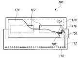
도 9는 본 발명에 따른 수직실장형 패키지(100)의 또 다른 실시예를 나타내는 평면도이다. 도 9를 참조하면, 본 실시예의 패키지(100)는 도 4 및 도 5에 도시된 패키지(50)와 그 구조가 유사하다. 즉, 상부면에 칩 패드(104)가 형성된 램버스 디램 칩(102)이 금속 방열판(120)에 부착되고, 인쇄회로기판(106)이 칩(102)의 외곽에 인접하여 방열판(120)의 일부와 접착된다. 인쇄회로기판(106)은 기판 패드(108), 접속 패드(110), 회로배선(112)을 포함하며, 칩 패드(104)와 기판 패드(108)는 금속 세선(116)에 의하여 연결된다. 금속 세선(116) 및 칩(102), 기판 패드(108), 회로배선(112)의 일부는 봉지수지(118)에 의하여 봉지된다.9 is a plan view showing another embodiment of a vertically mounted
반면에, 본 실시예의 패키지(100)가 전술한 패키지와 다른 점은 2개의 램버스 디램 칩(102)을 포함하고 있다는 점이다. 즉, 본 실시예는 램버스 디램을 채용한 멀티 칩 패키지(100; multi chip package)의 예를 보여준다. 본 발명에 따른 수직실장형 패키지는 본 실시예에서 보여 준 구조를 갖는 멀티 칩 패키지 뿐만 아니라, 방열판의 형태 및 크기, 인쇄회로기판의 형태 및 크기를 자유로이 변경함으로써 여러 가지 형태로 구현이 가능하다. 도 6 내지 도 8의 패키지(80)도 멀티 칩 패키지로의 응용이 가능하다.On the other hand, the
다음은 본 발명의 수직실장형 패키지를 이용한 패키지 모듈(module)에 대하여 설명하겠다. 도 10은, 예를 들어, 도 4 및 도 5의 수직실장형 패키지(50)를 복수개 구비하는 패키지 모듈(130)을 도시한 것이다. 즉, 전술한 바와 같이, 램버스 디램 칩(52)과 인쇄회로기판(56)과 방열판(70)을 포함하는 수직실장형 패키지(50)들이 각각의 인쇄회로기판(56)을 통하여 제2 회로기판(134)에 수직으로 실장된다. 각각의 패키지(50)들과 제2 회로기판(134) 간의 전기적 접속은 각각의 인쇄회로기판(56)에 형성된 접속 패드들(도시되지 않음)을 통하여 이루어진다. 제2 회로기판(134)은 다시 모 기판(도 5 및 도 8의 40)에 실장된다.Next, a package module using the vertically mounted package of the present invention will be described. FIG. 10 illustrates a
본 발명에 의한 패키지 모듈(130)은 각각의 방열판들(70)과 접착되는 방열 장치(132; heat sink)를 더 포함할 수 있다. 즉, 방열판(70)은 칩(52)과 인쇄회로기판(56)의 하부쪽(도 10에서는 오른쪽) 뿐만 아니라, 칩(52)을 사이에 두고 인쇄회로기판(56)의 반대쪽(즉, 패키지(50)가 수직으로 실장된 상태에서 패키지(50)의 상부쪽)으로도 연장되어 형성될 수 있다. 따라서 모듈(130)의 방열 장치(132)는 패키지(50) 상부로 연장된 방열판(70)에 쉽게 부착될 수 있으며, 열 방출 효과를 극대화할 수 있다. 본 실시예의 모듈(130)은 도 4와 도 5에 도시된 패키지(50)를 예로 들어 설명하였지만, 도 6 내지 도 8의 패키지(80)와, 도 9의 멀티 칩 패키지(100)를 비롯한 본 발명에 따른 다른 패키지들도 본 실시예처럼 패키지 모듈의 구현이 가능하다.The
도 11 및 도 12는 본 발명에 따른 수직실장형 패키지 및 패키지 모듈의 열 방출 효과를 알아보기 위하여 컴퓨터 모의실험을 한 결과 얻어진 온도 구배 분포도이다. 도 11은 도 4 및 도 5에 도시된 패키지, 도 12는 도 10에 도시된 모듈의 온도 구배 분포를 각각 보여주는 도들이다. 도 11과 도 12를 종래의 패키지를 통하여 실험한 도 3의 결과와 비교하여 설명하겠다.11 and 12 are temperature gradient distributions obtained as a result of computer simulation to examine the heat dissipation effect of the vertically mounted package and package module according to the present invention. 11 is a package showing the package shown in Figures 4 and 5, Figure 12 is a diagram showing the temperature gradient distribution of the module shown in Figure 10, respectively. 11 and 12 will be described in comparison with the results of FIG. 3 experimented through a conventional package.
열해석 모의실험 조건은 다음과 같다: 분위기 온도 = 60℃ (유속이 없는 자연대류조건), 동작 전력 = 2W (단, 모듈의 경우에는 실제 동작시 동작되는 1개의 패키지만 2W를 소모하고, 나머지 대기 상태의 7개의 패키지는 0.3W를 필요로 하기 때문에 4.1W를 입력하였다). 이와 같이 동일한 조건에서 각각 실험한 결과, 칩의 접합 온도(junction temperature), 즉 칩의 상부면에서 측정되는 온도는 종래의 패키지의 경우에 117.800℃(도 3 참조), 본 발명의 패키지의 경우에 107.090℃(도 11 참조), 본 발명의 모듈의 경우에 90.689℃(도 12 참조)가 각각 얻어졌다.Thermal simulation simulation conditions are as follows: Ambient temperature = 60 ° C (natural convection condition without flow rate), operating power = 2W (However, in the case of modules, only one package consumed during actual operation consumes 2W and the rest The seven packages in standby require 0.3W, so we entered 4.1W). As a result of each experiment under the same conditions, the junction temperature of the chip, that is, the temperature measured at the upper surface of the chip, is 117.800 ° C. (see FIG. 3) in the case of the conventional package, and in the case of the package of the present invention. 107.090 ° C (see FIG. 11) and 90.689 ° C (see FIG. 12) were obtained for the module of the present invention, respectively.
칩의 접합 온도가 낮다는 것은 그만큼 열 방출이 수월하게 이루어짐을 증명하는 것으로, 본 발명의 열 방출 특성이 향상됨을 알 수 있다. 특히, 패키지의 열저항값 θja(=[접합온도-분위기온도]/동작전력)은 종래의 경우 28.9℃/W, 본 발명의 경우 23.6℃/W로서, 본 발명에 의한 패키지가 종래의 패키지보다 약 20% 정도 열 방출 효과가 향상된다는 사실을 알 수 있다.The low junction temperature of the chip proves that the heat dissipation is easy, and it can be seen that the heat dissipation characteristics of the present invention are improved. In particular, the thermal resistance value θja (= [junction temperature-ambient temperature] / operating power) of the package is 28.9 ° C./W in the conventional case and 23.6 ° C./W in the present invention, and the package according to the present invention is a conventional package. It can be seen that the heat dissipation effect is improved by about 20%.
도 3, 도 11, 도 12의 등온선들은 각각 칩 접합 온도(●)로부터 분위기 온도(60℃)까지를 20등분하여, 각각 2.890℃, 2.355℃, 1.534℃의 간격을 두고 나타낸 것들이다. 예를 들어, 칩 접합 온도(●)로부터 1번째, 6번째, 11번째의 등온선을 ▲, □, ▽으로 표시하였으며, 그 온도를 기재하였다. 특히, 도 3과 도 11의 1번째 등온선을 서로 비교해 보면, 도 3의 1번째 등온선은 인쇄회로기판과 방열판의 접면 근방에 있지만, 도 11의 1번째 등온선은 방열판 외부의 대기 중에 있음을 볼 수 있다. 이는 종래의 패키지(도 3)보다 본 발명의 패키지(도 11)에서 더 열 방출이 잘 되고 있음을 다시 한번 확인시켜 주는 것이다.The isotherms of FIGS. 3, 11, and 12 are shown at intervals of 2.890 ° C., 2.355 ° C., and 1.534 ° C., respectively, by dividing the chip junction temperature (?) From the atmosphere temperature (60 ° C.) by 20 equal parts. For example, the 1st, 6th, and 11th isotherms were marked with ▲, □, and ▽ from the chip junction temperature (●), and the temperature was described. In particular, when comparing the first isotherm of FIGS. 3 and 11 with each other, the first isotherm of FIG. 3 is near the contact surface of the printed circuit board and the heat sink, but the first isotherm of FIG. 11 is in the atmosphere outside the heat sink. have. This confirms that heat dissipation is better in the package of the present invention (FIG. 11) than the conventional package (FIG. 3).
이상 설명한 바와 같이, 본 발명의 구조에 따르면, 반도체 칩을 직접 금속 방열판에 부착시키거나 여러 금속층을 포함하는 인쇄회로기판을 사용함으로써 열 방출 효과를 보다 효율적으로 거둘 수 있다.As described above, according to the structure of the present invention, the heat dissipation effect can be more efficiently achieved by directly attaching the semiconductor chip to the metal heat sink or by using a printed circuit board including several metal layers.
더욱이, 본 발명의 수직실장형 패키지를 모듈화해서 방열 장치를 추가로 부착할 수 있기 때문에 열 방출 효과가 배가될 수 있다.Moreover, the heat dissipation effect can be doubled because the vertically mounted package of the present invention can be modularized to further attach the heat dissipation device.
또한, 본 발명의 패키지는 열전도성 및 전기전도도가 우수한 구리배선을 미세패턴으로 형성할 수 있는 인쇄회로기판을 사용하기 때문에 우수한 전기적 특성을 나타낸다.In addition, the package of the present invention exhibits excellent electrical characteristics because it uses a printed circuit board capable of forming a copper pattern having excellent thermal conductivity and electrical conductivity in a fine pattern.
Claims (26)
Translated fromKoreanPriority Applications (4)
| Application Number | Priority Date | Filing Date | Title |
|---|---|---|---|
| KR1019970046367AKR100236671B1 (en) | 1997-09-09 | 1997-09-09 | Vertically mounted semiconductor chip package having a printed circuit board and a heat sink and a package module including the same |
| TW087102341ATW391043B (en) | 1997-09-09 | 1998-02-19 | Vertical semiconductor device package having printed circuit board and heat spreader, and module having the packages |
| JP10138121AJPH1187574A (en) | 1997-09-09 | 1998-05-20 | Vertically mounted semiconductor chip package and package module including the same |
| US09/144,510US6326686B1 (en) | 1997-09-09 | 1998-08-31 | Vertical semiconductor device package having printed circuit board and heat spreader, and module having the packages |
Applications Claiming Priority (1)
| Application Number | Priority Date | Filing Date | Title |
|---|---|---|---|
| KR1019970046367AKR100236671B1 (en) | 1997-09-09 | 1997-09-09 | Vertically mounted semiconductor chip package having a printed circuit board and a heat sink and a package module including the same |
Publications (2)
| Publication Number | Publication Date |
|---|---|
| KR19990024962A KR19990024962A (en) | 1999-04-06 |
| KR100236671B1true KR100236671B1 (en) | 2000-01-15 |
Family
ID=19521057
Family Applications (1)
| Application Number | Title | Priority Date | Filing Date |
|---|---|---|---|
| KR1019970046367AExpired - Fee RelatedKR100236671B1 (en) | 1997-09-09 | 1997-09-09 | Vertically mounted semiconductor chip package having a printed circuit board and a heat sink and a package module including the same |
Country Status (4)
| Country | Link |
|---|---|
| US (1) | US6326686B1 (en) |
| JP (1) | JPH1187574A (en) |
| KR (1) | KR100236671B1 (en) |
| TW (1) | TW391043B (en) |
Cited By (1)
| Publication number | Priority date | Publication date | Assignee | Title |
|---|---|---|---|---|
| US9257418B2 (en) | 2013-03-21 | 2016-02-09 | Samsung Electronics Co., Ltd. | Semiconductor package having heat slug and passive device |
Families Citing this family (13)
| Publication number | Priority date | Publication date | Assignee | Title |
|---|---|---|---|---|
| US6008074A (en)* | 1998-10-01 | 1999-12-28 | Micron Technology, Inc. | Method of forming a synchronous-link dynamic random access memory edge-mounted device |
| US6900719B2 (en)* | 2002-04-25 | 2005-05-31 | Roseman Engineering Ltd. | Method, device and system for providing anti-theft protection for electrical devices, particularly controllers in vehicle refueling systems |
| KR100631922B1 (en)* | 2004-02-23 | 2006-10-04 | 삼성전자주식회사 | Multilayer circuit boards with improved heat spreading performance and subsequent manufacturing |
| KR100558065B1 (en)* | 2004-03-15 | 2006-03-10 | 삼성전자주식회사 | Semiconductor Module with Heat Sink |
| DE102004019435A1 (en)* | 2004-04-19 | 2005-11-03 | Siemens Ag | On a cooling fin arranged component |
| US20060273450A1 (en)* | 2005-06-02 | 2006-12-07 | Intel Corporation | Solid-diffusion, die-to-heat spreader bonding methods, articles achieved thereby, and apparatus used therefor |
| CN101118458A (en)* | 2006-07-31 | 2008-02-06 | 华硕电脑股份有限公司 | Electronic device with temperature equalization plate |
| JP4937951B2 (en)* | 2008-03-25 | 2012-05-23 | 三菱電機株式会社 | Power semiconductor device and manufacturing method thereof |
| JP2010129806A (en)* | 2008-11-28 | 2010-06-10 | Mitsubishi Electric Corp | Power semiconductor device and process of manufacturing the same |
| JP2014110249A (en)* | 2012-11-30 | 2014-06-12 | Shindengen Electric Mfg Co Ltd | Structure for embedding semiconductor device, and method of embedding semiconductor device |
| TWI757654B (en)* | 2019-11-08 | 2022-03-11 | 立德電子股份有限公司 | Electrically and thermally conductive structures for high-power power supplies |
| CN113141122A (en)* | 2020-01-20 | 2021-07-20 | 珠海格力电器股份有限公司 | Intelligent power module and preparation method thereof |
| US20240306287A1 (en)* | 2023-03-08 | 2024-09-12 | Mellanox Technologies, Ltd. | Efficient thermal management for vertical power delivery |
Family Cites Families (4)
| Publication number | Priority date | Publication date | Assignee | Title |
|---|---|---|---|---|
| JPH0750753B2 (en)* | 1987-08-21 | 1995-05-31 | 株式会社東芝 | Transistor device |
| US5847467A (en)* | 1990-08-31 | 1998-12-08 | Texas Instruments Incorporated | Device packaging using heat spreaders and assisted deposition of wire bonds |
| US5773877A (en)* | 1997-02-07 | 1998-06-30 | Ford Motor Company | Plastic encapsulated IC package and method of designing same |
| US6008074A (en)* | 1998-10-01 | 1999-12-28 | Micron Technology, Inc. | Method of forming a synchronous-link dynamic random access memory edge-mounted device |
- 1997
- 1997-09-09KRKR1019970046367Apatent/KR100236671B1/ennot_activeExpired - Fee Related
- 1998
- 1998-02-19TWTW087102341Apatent/TW391043B/ennot_activeIP Right Cessation
- 1998-05-20JPJP10138121Apatent/JPH1187574A/enactivePending
- 1998-08-31USUS09/144,510patent/US6326686B1/ennot_activeExpired - Fee Related
Cited By (1)
| Publication number | Priority date | Publication date | Assignee | Title |
|---|---|---|---|---|
| US9257418B2 (en) | 2013-03-21 | 2016-02-09 | Samsung Electronics Co., Ltd. | Semiconductor package having heat slug and passive device |
Also Published As
| Publication number | Publication date |
|---|---|
| TW391043B (en) | 2000-05-21 |
| US6326686B1 (en) | 2001-12-04 |
| KR19990024962A (en) | 1999-04-06 |
| JPH1187574A (en) | 1999-03-30 |
Similar Documents
| Publication | Publication Date | Title |
|---|---|---|
| JP3762844B2 (en) | Opposite multichip package | |
| US5444296A (en) | Ball grid array packages for high speed applications | |
| TW415056B (en) | Multi-chip packaging structure | |
| US7396702B2 (en) | Module assembly and method for stacked BGA packages | |
| US5598031A (en) | Electrically and thermally enhanced package using a separate silicon substrate | |
| KR100586698B1 (en) | Semiconductor Module with Vertically Mounted Semiconductor Chip Package | |
| US5777345A (en) | Multi-chip integrated circuit package | |
| US6559525B2 (en) | Semiconductor package having heat sink at the outer surface | |
| US7202561B2 (en) | Semiconductor package with heat dissipating structure and method of manufacturing the same | |
| KR100236671B1 (en) | Vertically mounted semiconductor chip package having a printed circuit board and a heat sink and a package module including the same | |
| US5978224A (en) | Quad flat pack integrated circuit package | |
| US5349235A (en) | High density vertically mounted semiconductor package | |
| US6600651B1 (en) | Package with high heat dissipation | |
| US6392896B1 (en) | Semiconductor package containing multiple memory units | |
| GB2274738A (en) | Cooling for 3-D semiconductor packages | |
| US6137174A (en) | Hybrid ASIC/memory module package | |
| KR19990026510A (en) | Vertical mount semiconductor package module with external heat sink | |
| KR100195504B1 (en) | Heat Dissipation Ball Grid Array (BGA) Package | |
| CN223450885U (en) | Integrated circuit chip packaging structure | |
| US20020050378A1 (en) | Double-layered multiple chip module package | |
| KR19990028206U (en) | Stacked Semiconductor Packages | |
| JP3460930B2 (en) | Electronic circuit package | |
| KR20020088300A (en) | Semiconductor package with heat spreader using cooling material | |
| JPS61253843A (en) | Semiconductor device | |
| KR200180815Y1 (en) | Semiconductor package having capacitor |
Legal Events
| Date | Code | Title | Description |
|---|---|---|---|
| A201 | Request for examination | ||
| PA0109 | Patent application | St.27 status event code:A-0-1-A10-A12-nap-PA0109 | |
| PA0201 | Request for examination | St.27 status event code:A-1-2-D10-D11-exm-PA0201 | |
| R17-X000 | Change to representative recorded | St.27 status event code:A-3-3-R10-R17-oth-X000 | |
| R18-X000 | Changes to party contact information recorded | St.27 status event code:A-3-3-R10-R18-oth-X000 | |
| PN2301 | Change of applicant | St.27 status event code:A-3-3-R10-R13-asn-PN2301 St.27 status event code:A-3-3-R10-R11-asn-PN2301 | |
| PG1501 | Laying open of application | St.27 status event code:A-1-1-Q10-Q12-nap-PG1501 | |
| PN2301 | Change of applicant | St.27 status event code:A-3-3-R10-R13-asn-PN2301 St.27 status event code:A-3-3-R10-R11-asn-PN2301 | |
| E701 | Decision to grant or registration of patent right | ||
| PE0701 | Decision of registration | St.27 status event code:A-1-2-D10-D22-exm-PE0701 | |
| GRNT | Written decision to grant | ||
| PR0701 | Registration of establishment | St.27 status event code:A-2-4-F10-F11-exm-PR0701 | |
| PR1002 | Payment of registration fee | St.27 status event code:A-2-2-U10-U11-oth-PR1002 Fee payment year number:1 | |
| PG1601 | Publication of registration | St.27 status event code:A-4-4-Q10-Q13-nap-PG1601 | |
| R18-X000 | Changes to party contact information recorded | St.27 status event code:A-5-5-R10-R18-oth-X000 | |
| PN2301 | Change of applicant | St.27 status event code:A-5-5-R10-R13-asn-PN2301 St.27 status event code:A-5-5-R10-R11-asn-PN2301 | |
| PR1001 | Payment of annual fee | St.27 status event code:A-4-4-U10-U11-oth-PR1001 Fee payment year number:4 | |
| R18-X000 | Changes to party contact information recorded | St.27 status event code:A-5-5-R10-R18-oth-X000 | |
| R18-X000 | Changes to party contact information recorded | St.27 status event code:A-5-5-R10-R18-oth-X000 | |
| PR1001 | Payment of annual fee | St.27 status event code:A-4-4-U10-U11-oth-PR1001 Fee payment year number:5 | |
| R18-X000 | Changes to party contact information recorded | St.27 status event code:A-5-5-R10-R18-oth-X000 | |
| PR1001 | Payment of annual fee | St.27 status event code:A-4-4-U10-U11-oth-PR1001 Fee payment year number:6 | |
| PN2301 | Change of applicant | St.27 status event code:A-5-5-R10-R13-asn-PN2301 St.27 status event code:A-5-5-R10-R11-asn-PN2301 | |
| PN2301 | Change of applicant | St.27 status event code:A-5-5-R10-R13-asn-PN2301 St.27 status event code:A-5-5-R10-R11-asn-PN2301 | |
| PR1001 | Payment of annual fee | St.27 status event code:A-4-4-U10-U11-oth-PR1001 Fee payment year number:7 | |
| PR1001 | Payment of annual fee | St.27 status event code:A-4-4-U10-U11-oth-PR1001 Fee payment year number:8 | |
| FPAY | Annual fee payment | Payment date:20071001 Year of fee payment:9 | |
| PR1001 | Payment of annual fee | St.27 status event code:A-4-4-U10-U11-oth-PR1001 Fee payment year number:9 | |
| LAPS | Lapse due to unpaid annual fee | ||
| PC1903 | Unpaid annual fee | St.27 status event code:A-4-4-U10-U13-oth-PC1903 Not in force date:20081005 Payment event data comment text:Termination Category : DEFAULT_OF_REGISTRATION_FEE | |
| PC1903 | Unpaid annual fee | St.27 status event code:N-4-6-H10-H13-oth-PC1903 Ip right cessation event data comment text:Termination Category : DEFAULT_OF_REGISTRATION_FEE Not in force date:20081005 | |
| R18-X000 | Changes to party contact information recorded | St.27 status event code:A-5-5-R10-R18-oth-X000 |