KR100235594B1 - Liquid crystal display and method for manufacturing the same - Google Patents
Liquid crystal display and method for manufacturing the sameDownload PDFInfo
- Publication number
- KR100235594B1 KR100235594B1KR1019970004290AKR19970004290AKR100235594B1KR 100235594 B1KR100235594 B1KR 100235594B1KR 1019970004290 AKR1019970004290 AKR 1019970004290AKR 19970004290 AKR19970004290 AKR 19970004290AKR 100235594 B1KR100235594 B1KR 100235594B1
- Authority
- KR
- South Korea
- Prior art keywords
- gate
- pad
- conductive material
- source
- electrode
- Prior art date
- Legal status (The legal status is an assumption and is not a legal conclusion. Google has not performed a legal analysis and makes no representation as to the accuracy of the status listed.)
- Expired - Lifetime
Links
Images


Classifications
- G—PHYSICS
- G02—OPTICS
- G02F—OPTICAL DEVICES OR ARRANGEMENTS FOR THE CONTROL OF LIGHT BY MODIFICATION OF THE OPTICAL PROPERTIES OF THE MEDIA OF THE ELEMENTS INVOLVED THEREIN; NON-LINEAR OPTICS; FREQUENCY-CHANGING OF LIGHT; OPTICAL LOGIC ELEMENTS; OPTICAL ANALOGUE/DIGITAL CONVERTERS
- G02F1/00—Devices or arrangements for the control of the intensity, colour, phase, polarisation or direction of light arriving from an independent light source, e.g. switching, gating or modulating; Non-linear optics
- G02F1/01—Devices or arrangements for the control of the intensity, colour, phase, polarisation or direction of light arriving from an independent light source, e.g. switching, gating or modulating; Non-linear optics for the control of the intensity, phase, polarisation or colour
- G02F1/13—Devices or arrangements for the control of the intensity, colour, phase, polarisation or direction of light arriving from an independent light source, e.g. switching, gating or modulating; Non-linear optics for the control of the intensity, phase, polarisation or colour based on liquid crystals, e.g. single liquid crystal display cells
- G02F1/133—Constructional arrangements; Operation of liquid crystal cells; Circuit arrangements
- G02F1/136—Liquid crystal cells structurally associated with a semi-conducting layer or substrate, e.g. cells forming part of an integrated circuit
- G02F1/1362—Active matrix addressed cells
- G02F1/136286—Wiring, e.g. gate line, drain line
- G—PHYSICS
- G02—OPTICS
- G02F—OPTICAL DEVICES OR ARRANGEMENTS FOR THE CONTROL OF LIGHT BY MODIFICATION OF THE OPTICAL PROPERTIES OF THE MEDIA OF THE ELEMENTS INVOLVED THEREIN; NON-LINEAR OPTICS; FREQUENCY-CHANGING OF LIGHT; OPTICAL LOGIC ELEMENTS; OPTICAL ANALOGUE/DIGITAL CONVERTERS
- G02F1/00—Devices or arrangements for the control of the intensity, colour, phase, polarisation or direction of light arriving from an independent light source, e.g. switching, gating or modulating; Non-linear optics
- G02F1/01—Devices or arrangements for the control of the intensity, colour, phase, polarisation or direction of light arriving from an independent light source, e.g. switching, gating or modulating; Non-linear optics for the control of the intensity, phase, polarisation or colour
- G02F1/13—Devices or arrangements for the control of the intensity, colour, phase, polarisation or direction of light arriving from an independent light source, e.g. switching, gating or modulating; Non-linear optics for the control of the intensity, phase, polarisation or colour based on liquid crystals, e.g. single liquid crystal display cells
- G02F1/133—Constructional arrangements; Operation of liquid crystal cells; Circuit arrangements
- G02F1/1333—Constructional arrangements; Manufacturing methods
- G02F1/1343—Electrodes
- H—ELECTRICITY
- H10—SEMICONDUCTOR DEVICES; ELECTRIC SOLID-STATE DEVICES NOT OTHERWISE PROVIDED FOR
- H10D—INORGANIC ELECTRIC SEMICONDUCTOR DEVICES
- H10D30/00—Field-effect transistors [FET]
- H10D30/60—Insulated-gate field-effect transistors [IGFET]
- H10D30/67—Thin-film transistors [TFT]
Landscapes
- Physics & Mathematics (AREA)
- Nonlinear Science (AREA)
- Mathematical Physics (AREA)
- Chemical & Material Sciences (AREA)
- Crystallography & Structural Chemistry (AREA)
- General Physics & Mathematics (AREA)
- Optics & Photonics (AREA)
- Engineering & Computer Science (AREA)
- Microelectronics & Electronic Packaging (AREA)
- Liquid Crystal (AREA)
- Thin Film Transistor (AREA)
Abstract
Translated fromKoreanDescription
Translated fromKorean본 발명은 박막 트랜지스터(혹은 Thin Film Transistor(TFT))와 상기 박막 트랜지스터에 연결된 화소 전극이 행렬 방식으로 배열된 액티브 패널을 포함하는 능동 매트릭스 액정 표시 장치(또는 Active Matrix Liquid Crystal Display, 이하 액정표시 장치 혹은 AMLCD로 표기함)를 제조하는 방법에 관련된 것이다. 특히, 본 발명은 능동 매트릭스 액정 표시 장치를 제조하는데 있어서 마스크 공정의 수를 줄여 제조 공정을 단순화하는 방법에 관련된 것이다.The present invention relates to an active matrix liquid crystal display (or active matrix liquid crystal display) device including a thin film transistor (or thin film transistor (TFT)) and an active panel in which pixel electrodes connected to the thin film transistor are arranged in a matrix manner. Or AMLCD). In particular, the present invention relates to a method of simplifying the manufacturing process by reducing the number of mask processes in manufacturing an active matrix liquid crystal display.
화상 정보를 화면에 나타내는 화면 표시 장치들 중에서, 박막형 평판 표시 장치가 가볍고, 어느 장소에든지 쉽게 사용할 수 있다는 장점 때문에 근래에 집중적인 개발의 대상이 되고 있다. 특히, 액정 표시 장치는 해상도가 높고, 동화상을 실현하기에 충분할 만큼 반응 속도가 빠르기 때문에, 가장 활발한 연구가 이루어지고 있는 제품이다.Among the screen display devices that display image information on the screen, the thin-film flat panel display device has become an object of intensive development in recent years because of its advantages of being lightweight and easily used anywhere. In particular, the liquid crystal display device has a high resolution and a reaction rate is fast enough to realize a moving picture, and thus the most active research is made.
액정 표시 장치의 원리는 액정의 광학적 이방성과 분극 성질을 이용한 것이다. 방향성을 갖고 있는 액정 분자의 배향 방향을 분극성을 이용하여 인위적으로 조절함으로써, 배향 방향에 따른 광학적 이방성으로 빛의 투과, 차단이 가능하다. 이것을 응용하여 화면 표시 장치로 사용한다. 현재에는 박막 트랜지스터와 그것에 연결된 화소 전극이 행렬 방식으로 배열된 능동 매트릭스 액정 표시 장치가 뛰어난 화질을 제공하기 때문에 가장 많이 사용되고 있다. 일반적인 액정 표시 장치의 구조를 자세히 살펴보면 다음과 같다.The principle of the liquid crystal display device is to use the optical anisotropy and polarization properties of the liquid crystal. By artificially adjusting the alignment direction of liquid crystal molecules having directionality using polarization, light can be transmitted and blocked with optical anisotropy according to the alignment direction. Use this as a screen display device. Currently, an active matrix liquid crystal display in which thin film transistors and pixel electrodes connected thereto are arranged in a matrix manner is used most often because it provides excellent image quality. Looking at the structure of a general liquid crystal display device in detail as follows.
액정 표시 장치의 한쪽 패널(혹은 칼라 필터 패널)은 투명 기판 위에 픽셀의 위치에 빨강(R), 초록(G), 파랑(B)의 칼라 필터가 순차적으로 배치된 구조로 이루어져 있다. 이들 칼라 필터 사이에는 블랙 매트릭스가 그물 모양으로 형성되어 있다. 그리고, 이들 칼라 필터 위에 공통 전극이 형성되어 있다. 액정 표시 장치의 다른 쪽 패널(혹은 액티브 패널)은 투명 기판 위에 행렬 방식으로 설계된 화소의 위치에 화소 전극들이 배열된 구조로 이루어져 있다. 화소 전극의 수평 방향을 따라서 신호배선이 형성되어 있고, 수직 방향을 따라서 데이터 배선이 형성되어 있다. 화소 전극의 한쪽 구석에는 화소 전극을 구동하기 위한 박막 트랜지스터가 형성되어 있다.One panel (or color filter panel) of the liquid crystal display device has a structure in which color filters of red (R), green (G), and blue (B) are sequentially arranged at positions of pixels on a transparent substrate. A black matrix is formed in a mesh shape between these color filters. And a common electrode is formed on these color filters. The other panel (or active panel) of the liquid crystal display has a structure in which pixel electrodes are arranged at positions of pixels designed in a matrix manner on a transparent substrate. Signal wirings are formed along the horizontal direction of the pixel electrode, and data wirings are formed along the vertical direction. In one corner of the pixel electrode, a thin film transistor for driving the pixel electrode is formed.
박막 트랜지스터의 게이트 전극은 신호 배선에 연결되어 있고(따라서, "게이트 배선"이라고 부르기도 한다), 박막 트랜지스터의 소스 전극이 데이터 배선에 연결되어 있다(따라서, "데이터 배선" 혹은 "소스 배선"이라고 부르기도 한다). 그리고, 각 배선의 끝단에는 외부의 구동 회로와 연결하기 위한 패드부가 형성된다.The gate electrode of the thin film transistor is connected to the signal wiring (henceforth referred to as gate wiring), and the source electrode of the thin film transistor is connected to the data wiring (thus referred to as "data wiring" or "source wiring". Also called). At the end of each wiring, a pad portion for connecting with an external driving circuit is formed.
이러한 구조를 갖는 두 개의 패널이 일정 간격(이 간격을 "셀 갭(cell gap)"이라고 부른다)을 두고 서로 대향하여 부착되고, 그 사이에 액정 물질이 채워진다.Two panels having such a structure are attached to each other at a predetermined interval (referred to as a "cell gap"), and the liquid crystal material is filled therebetween.
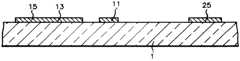
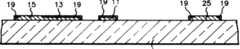
액정 표시 장치를 제조하는 공정은 매우 복잡하며, 여러 가지 공정들이 복합적으로 이루어져 있다. 특히, 박막 트랜지스터와 화소 전극이 형성되는 액티브 패널을 제조하는데는 여러 제조 공정을 거쳐서 이루어진다. 액티브 패널에는 액정 표시 장치의 중요한 소자들이 많이 만들어지고, 복잡한 공정을 여러 번 거치므로, 이것을 단순화하는 방법을 개발하는 것이 상당히 중요하다. 우선, 일반적인 액티브 패널의 평면도를 나타내는 제1도, 제1도에서 Ⅱ-Ⅱ 절단선으로 자른 단면으로 제조 공정을 나타내는 제2도를 이용하여 종래의 액티브 패널 제조 방법에 대하여 설명한다.The process of manufacturing the liquid crystal display is very complicated, and various processes are combined. In particular, the active panel in which the thin film transistor and the pixel electrode are formed is made through various manufacturing processes. In the active panel, many important elements of the liquid crystal display are made, and a complicated process is repeated many times, so it is very important to develop a method of simplifying this. First, the conventional active panel manufacturing method is demonstrated using FIG. 1 which shows the top view of a general active panel, and FIG. 2 which shows a manufacturing process with the cross section cut by the II-II cutting line in FIG.
투명 유리 기판(1)에 알루미늄 혹은 알루미늄 합금 등을 증착하고, 포토 리소그래피(Photo Lithography-사진 식각) 법으로 패턴하여 게이트 전극(11), 게이트 배선(13), 게이트 패드(15), 소스 패드(25) 그리고 단락 배선(혹은, Shorting Bar)(45) 등을 형성한다. 상기 게이트 전극(11)은 행렬 배열 방식으로 설계된 화소의 한쪽 구석에 형성된다. 상기 게이트 배선(13)은 행 방향으로 배열된 게이트 전극(11)들을 연결하고 있다. 상기 게이트 패드(15)는 상기 게이트 배선(13)의 끝 부분에 형성되고, 상기 단락 배선(45)은 게이트 패드(15)들과 소스 패드(25)들을 서로 연결하고 있다. 상기 소스 패드(25)는 나중에 형성되는 소스 배선(25)들의 끝 부분에 형성된다(제2a도).Aluminum or an aluminum alloy is deposited on the
상기 단락 배선(45)을 전극으로 이용하여 상기 알루미늄을 포함하는 금속으로 형성된 소자들을 양극 산화하여 표면에 양극 산화막(19)을 형성한다. 이것은 알루미늄의 표면에 힐락(Hillock)이 성장하는 것을 방지하기 위한 공정이다. 이 때 포토 레지스트를 패턴한 마스크로 양극 산화되면 안되는 부분을 가리고 양극 산화 공정을 수행한다. 따라서, 상기 게이트 패드(15)와 소스 패드(25)의 표면에 양극 산화막(19)이 형성되지 않도록 한다. 그 결과 박막 트랜지스터가 형성되는 부분은 제2b도에서처럼 기판(1) 위에 양극 산화막(19)을 포함하는 게이트 전극(11)이 형성된다. 표면에 양극 산화막(19)을 포함하는 게이트 배선(13)이 형성되어 있다. 상기 게이트 배선(13)에 연결되며 표면에 양극 산화막이 형성되지 않은 게이트 패드(15) 그리고, 상기 게이트 패드들을 연결하는 단락 배선(45)이 형성된다. 그리고, 게이트 패드(15)와 비슷한 형태로 표면에 양극 산화막(19)이 형성되지 않은 소스 패드(25)와 상기 소스 패드들을 연결하는 단락 배선(45)이 형성된다(제1도, 제2b도).An
그리고, 상기 소자들이 형성된 기판(1) 전면에 산화 실리콘이나, 질화 실리콘을 증착하여 게이트 절연막(17)을 형성한다. 그리고, 그 위에 진성 반도체 물질과 불순물이 첨가된 반도체 물질을 연속으로 증착하고, 포토 리소그래피 법으로 패턴하여 반도체 층(31), 불순물 반도체 층(33)을 형성한다(제2c도).The
그 후에 포토 리소그래피 법으로 게이트 절연막을 식각하여 게이트 패드(15)에는 제1게이트 콘택 홀(51)을, 소스 패드(25)에는 제1소스 콘택 홀(61)을 형성한다. 이 때 형성되는 콘택 홀(51, 61)들은 앞에서 양극 산화하지 않은 게이트 패드(15)부분과, 소스 패드(25) 부분이 드러나도록 형성한다(제2d도).Thereafter, the gate insulating layer is etched by photolithography to form a first
그리고, 크롬이나 크롬 합금과 같은 금속 등을 증착하고 패턴하여, 불순물 반도체 층(33) 위에는 소스 전극(21)과 드레인 전극(31)을 형성한다. 박막 트랜지스터가 형성되는 부분에서는 소스 전극(21)과 드레인 전극(31) 밑에 있는 불순물 반도체 층(27)이 연결되지 않도록 하기 위해서 소스(21)-드레인 전극(31)을 마스크로 하여 불순물 반도체 층을 식각하여 분리한다. 그리고 상기 소스 전극(21)들을 연결하는 소스 배선(23)을 형성한다. 그리고, 제1소스 콘택 홀(61)을 통해 소스 배선(23)과 소스 패드(25)를 연결시킨다. 이 때, 소스 패드(25)에는 알루미늄을 보호하기 위해 충분한 크기로 크롬 금속 층을 형성하여, 나중에 형성되는 소스 패드 연결 단자와 접속하기 위한 소스 패드 중간 전극(65)으로 사용하기도 한다. 마찬가지로 게이트 패드(15)에도 크롬 금속 층으로 알루미늄 층과 나중에 형성되는 게이트 패드 연결 단자와 제1게이트 콘택 홀(51)을 통해 접속되는 게이트 패드 중간 전극(55)을 형성한다(제2e도).A metal such as chromium or a chromium alloy is deposited and patterned to form a
그리고, 산화 실리콘이나 질화 실리콘 등과 같은 절연 물질을 전면에 증착하여 보호막(41)을 형성한다. 포토 리소그래피 법으로 상기 보호막(41)을 식각하여 게이트 패드(15)에 제2게이트 콘택 홀(53), 소스 패드(25)에 제2소스 콘택 홀(63), 그리고 드레인 전극(31)에 드레인 콘택 홀(71)을 형성한다. 제2게이트 콘택 홀(53)은 상기 게이트 패드 중간 전극(55)을 노출시키고, 제2소스 콘택 홀(63)은 상기 소스패드 중간 전극(65)을 노출시키는 것이다. 드레인 콘택 홀(71)은 상기 드레인 전극(31)의 일부를 노출시킨다(제2f도).The
상기 알루미늄을 포함하는 금속으로 형성한 게이트 배선(13), 게이트 전극(11), 게이트 패드(15), 소스 패드(25)들은 양극 산화를 위해 형성했던 단락 배선(45)에 의해 서로 연결되어 있는데, 이들이 모두 연결되어 있다면, 최종 제품에서는 정상적인 기능을 나타내지 못하므로, 필요 없이 연결된 부분들을 끊는다. 이 때, 포토 리소그래피 법으로 끊어주어야 할 부분(제1도의 A)들을 제거하든지 아니면, 단락 배선(45)을 모두 제거한다(도면에 나타나지 않음).The
그리고, ITO(Indium-Tin-Oxide)를 전면 증착하고, 패턴하여 화소 전극(33), 게이트 패드 연결 단자(57), 그리고 소스 패드 연결 단자(67)들을 형성한다. 화소 전극(33)은 상기 드레인 콘택 홀(71)을 통하여 상기 드레인 전극(31)과 전기적으로 연결되어 있다. 그리고, 게이트 패드 연결 단자(57)는 상기 제2게이트 콘택홀(53)을 통하여 상기 게이트패드 중간전극(55)에 전기적으로 연결되고, 소스 패드 연결 단자(67)는 상기 제2 소스 콘택 홀(63)을 통하여 상기 소스 패드 중간 전극(65)에 전기적으로 연결된다(제2g도).An ITO (Indium-Tin-Oxide) is deposited on the entire surface and patterned to form the
이상에서 액정 표시 장치의 액티브 패널을 제조하는 방법을 살펴보았듯이 제조공정은 각 박막들을 설계된 형상으로 형성하기 위해서 마스크를 사용하는 식각 법을 적어도 7번 내지 8번 사용하였다. 마스크 공정이 많아질수록 제조물의 정밀도는 떨어질 것이고, 따라서 AMLCD의 화질이 저하될 것이다. 또한, 하나의 마스크 공정에 소요되는 작업 조건에 따라 다르기는 하겠지만, 다른 공정에 비해 상당히 오래 걸린다. 따라서, 마스크 공정을 하나만 감소시킬 수 있다면, 제조 비용은 그 만큼 절감되고, 제조 수율은 그 만큼 증가한다.As described above, the method of manufacturing the active panel of the liquid crystal display device used the etching method using a mask at least 7 to 8 times in order to form each thin film into a designed shape. The more the mask process, the less will be the precision of the product, and thus the lower the quality of the AMLCD. In addition, although depending on the operating conditions required for one mask process, it takes considerably longer than other processes. Thus, if only one mask process can be reduced, the manufacturing cost is reduced by that amount, and the manufacturing yield increases by that amount.
따라서, 본 발명의 목적은 액정 표시 장치를 제조하는 방법을 단순화하는데 있다. 본 발명의 다른 목적은 액정 표시 장치의 액티브 패널을 제작하는데 있어서 사용되는 마스크 공정 수를 줄임으로써 전체 제조 공정을 단순화하는데 있다.Accordingly, an object of the present invention is to simplify the method of manufacturing the liquid crystal display device. Another object of the present invention is to simplify the entire manufacturing process by reducing the number of mask processes used in manufacturing the active panel of the liquid crystal display.
제1도는 종래 액티브 기판의 부분을 나타내는 평면 확대도이다.1 is an enlarged plan view showing a portion of a conventional active substrate.
제2도는 종래 액티브 기판의 제조 과정을 나타내는 단면 확대도이다.2 is an enlarged cross-sectional view illustrating a manufacturing process of a conventional active substrate.
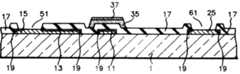
제3도는 본 발명에 의한 액티브 기판의 한 부분을 나타내는 평면 확대도이다.3 is an enlarged plan view showing a part of an active substrate according to the present invention.
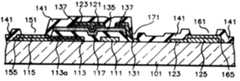
제4도는 본 발명의 첫 번째 예에 의한 액티브 기판의 제조 과정을 나타내는 단면도이다.4 is a cross-sectional view showing a manufacturing process of an active substrate according to a first example of the present invention.
제5도는 본 발명의 두 번째 예에 의한 액티브 기판의 제조 과정을 나타내는 단면도이다.5 is a cross-sectional view showing a manufacturing process of an active substrate according to a second example of the present invention.
* 도면의 주요부분에 대한 부호의 설명* Explanation of symbols for main parts of the drawings
1, 101 : 기판 11, 111 : 게이트 전극1, 101:
111a : 저 저항 게이트 전극 45 : 단락 배선(Shorting Bar)111a: low resistance gate electrode 45: shorting wiring (Shorting Bar)
13, 113 : 게이트 배선 113a : 저 저항 게이트 배선13, 113:
15, 115 : 게이트 패드 115a : 저 저항 게이트 패드15, 115:
17, 117 : 게이트 절연막 19 : 양극 산화막17, 117: gate insulating film 19: anodic oxide film
21, 121 : 소스 전극 23, 123 : 소스 배선21, 121:
25, 125 : 소스 패드 125a : 저 저항 소스 패드25, 125:
31, 131 : 반도체 층 33, 133 : 화소 전극31 and 131: semiconductor layers 33 and 133: pixel electrodes
35, 135 : 반도체 층 37, 137 : 불순물 반도체 층35, 135: semiconductor layers 37, 137: impurity semiconductor layers
41, 141 : 보호막 51 : 제1게이트 콘택홀41, 141: passivation layer 51: the first gate contact hole
53 : 제2게이트 콘택 홀 55, 155 : 게이트 패드 중간 전극53: second
57, 157 : 게이트 패드 연결 단자57, 157: Gate pad connection terminal
61 : 제1소스 콘택 홀 63 : 제2소스 콘택 홀61: first source contact hole 63: second source contact hole
65, 165 : 소스 패드 중간 전극 67, 167 : 소스 패드 연결 단다65, 165: source pad
71, 171 : 드레인 콘택 홀71, 171: drain contact hole
151 : 게이트 패드 콘택 홀 161 : 소스 패드 콘택 홀151: gate pad contact hole 161: source pad contact hole
본 발명은 액정 표시 장치를 제조하는데 있어서, 우리는 다음과 같은 방법을 제공하여 마스크 공정 수를 줄임으로써 단순화된 방법으로 액정 표시 장치의 액티브 패널을 제조할 수 있도록 한다.In the present invention, in manufacturing a liquid crystal display device, we provide the following method so that the active panel of the liquid crystal display device can be manufactured in a simplified manner by reducing the number of mask processes.
마스크 수를 줄이기 위해 본 발명에서는 첫째, 양극 산화하지 않는다. 그러므로, 나중에 양극 산화를 위한 단락 배선을 형성하지 않게 되고, 따라서 액정 패널 제조공정 중에 필요 없이 연결된 부분을 단선(Cut) 혹은 제거하는 공정이 필요하지 않게된다. 그리고, 본 발명에서는 알루미늄 금속을 양극 산화하여 힐락을 방지하는 대신에 알루미늄 금속을 덮는 제2금속을 이용하여 힐락을 방지한다. 즉, 게이트 배선구조를 표면 안정성은 떨어지더라도 저항이 낮은 금속 층과 저항이 다소 크지만 표면 안정성이 좋은 보호성 금속 층을 사용한 2중 금속 층으로 형성한다.In order to reduce the number of masks, the present invention does not first anodize. Therefore, a short circuit for anodic oxidation is not formed later, thus eliminating the need to cut or remove the connected portion without the need for the liquid crystal panel manufacturing process. In the present invention, instead of anodizing the aluminum metal to prevent hillock, the second metal covering the aluminum metal is used to prevent hillock. That is, the gate wiring structure is formed of a metal layer having a low resistance even though the surface stability is poor and a double metal layer using a protective metal layer having a large resistance but good surface stability.
둘째, 게이트 패드와 소스 패드에 게이트 절연막을 형성하지 않는다. 그럼으로써, 게이트 패드와 소스 패드에 외부 연결 단자와 연결하기 위한 콘택 홀을 형성하는 단계에서, 보호막에만 콘택 홀을 형성하게 되어 마스크 공정을 하나 줄일 수 있다.Second, a gate insulating film is not formed on the gate pad and the source pad. As a result, in forming the contact hole for connecting the external connection terminal to the gate pad and the source pad, the contact hole is formed only in the passivation layer, thereby reducing the mask process.
즉, 본 발명은 단선 공정이 생략되고, 패드 연결을 위한 콘택 홀을 형성하는 공정에서 마스크 공정 수가 하나 줄어든 단순 제조 공정을 제공하고 있다.That is, the present invention provides a simple manufacturing process in which the disconnection process is omitted and the number of mask processes is reduced by one in the process of forming contact holes for pad connection.
기판 위에 제1금속을 증착하고, 패턴하여 저 저항 게이트 배선을 형성한다. 제2 금속을 상기 게이트 배선이 형성된 기판 전면에 증착하고, 패턴하여 게이트 전극과 게이트 패드, 소스 패드 그리고, 상기 저 저항 배선을 덮는 게이트 배선을 형성한다. 절연 물질, 진성 반도체 물질 그리고, 불순물이 첨가된 반도체 물질을 상기 게이트 전극, 게이트 배선, 게이트 패드 그리고, 소스 패드가 형성된 기판 전면에 연속증착하고 패턴하여 게이트 절연막, 반도체 층 그리고, 불순물 반도체 층을 형성한다. 이 때, 게이트 패드와 소스 패드 부분은 게이트 절연막이 완전히 제거되어 노출된 상태가 되도록 한다. 제3 금속을 상기 반도체 층이 형성된 기판 전면에 증착하고, 패턴하여 소스 전극, 드레인 전극, 그리고, 소스 배선을 형성한다. 이 때, 노출된 게이트 패드와 소스 패드를 덮는 게이트 패드 중간 전극과 소스 패드 중간 전극을 형성한다. 상기 소스 전극 등이 형성된 기판 전면에 절연 물질을 증착하여 보호막을 형성한다. 패턴하여 상기 드레인 전극과, 소스 패드 중간 전극 그리고, 상기 게이트 패드 중간 전극을 덮고 있는 상기 보호막의 일부를 제거하여 콘택 홀을 형성한다. 상기 보호막 위에 도전성 물질을 전면 증착하고, 패턴하여 상기 콘택 홀에 의해 드레인 전극과 연결된 화소 전극과 게이트 패드 중간 전극에 연결된 게이트 패드 연결 단자 및 소스 패드 중간 전극에 연결된 소스 패드 연결 단자를 형성한다.The first metal is deposited on the substrate and patterned to form a low resistance gate wiring. A second metal is deposited on the entire surface of the substrate on which the gate wiring is formed and patterned to form a gate electrode, a gate pad, a source pad, and a gate wiring covering the low resistance wiring. An insulating material, an intrinsic semiconductor material, and a semiconductor material to which impurities are added are continuously deposited and patterned on the entire surface of the substrate on which the gate electrode, the gate wiring, the gate pad, and the source pad are formed, thereby forming a gate insulating film, a semiconductor layer, and an impurity semiconductor layer. do. At this time, the gate pad and the source pad portion are in a state where the gate insulating film is completely removed. A third metal is deposited on the entire surface of the substrate on which the semiconductor layer is formed, and is patterned to form a source electrode, a drain electrode, and a source wiring. At this time, the gate pad intermediate electrode and the source pad intermediate electrode covering the exposed gate pad and the source pad are formed. A protective film is formed by depositing an insulating material on the entire surface of the substrate on which the source electrode and the like are formed. A contact hole is formed by patterning a portion of the passivation layer covering the drain electrode, the source pad intermediate electrode, and the gate pad intermediate electrode. A conductive material is deposited on the passivation layer and patterned to form a gate pad connection terminal connected to the pixel electrode connected to the drain electrode, a gate pad intermediate electrode, and a source pad connection terminal connected to the source pad intermediate electrode by the contact hole.
본 발명에서 제공하는 단순화된 공정으로 액티브 패널을 제조하기 위한 구체적인 공정 방법들을 다음 실시 예들을 이용하여 자세히 설명한다.Specific process methods for manufacturing the active panel by the simplified process provided by the present invention will be described in detail using the following embodiments.
[실시예 1]Example 1
본 실시예의 이해를 돕기 위해서 액정 표시 장치의 평면도를 나타내는 제3도과, 제3도의 절단선 Ⅳ-Ⅳ으로 절단한 공정 단면도인 제4도를 이용하여 설명한다.For better understanding of the present embodiment, a description will be given using FIG. 3 showing a plan view of the liquid crystal display and FIG. 4, which is a cross sectional view taken along the cut line IV-IV of FIG.
투명 유리 기판(101)위에 알루미늄이나 알룸미늄 합금을 증착하고, 포토 리소그래피 법으로 패턴하여 저 저항 게이트 버스 배선(113a)을 형성한다(제3도, 제4a도).Aluminum or aluminum alloy is deposited on the
그리고, 크롬(Cr), 몰리브덴(Mo), 탄탈(Ta) 혹은 주석(Sb)을 포함하는 금속을 상기 저 저항 게이트 버스 배선(113a)이 형성된 기판 전면에 증착하고, 패턴하여 게이트 전극(111)과, 게이트 패드(115) 그리고, 소스 패드(125)를 형성한다. 이 때 저 저항 게이트 배선(113a)에는 상기 알루미늄을 포함하는 금속 층을 덮도록 크롬을 패턴하여 알루미늄 표면에 힐락이 발생하지 않도록 보호하는 게이트 배선(113)을 형성한다(제4b도).A metal including chromium (Cr), molybdenum (Mo), tantalum (Ta), or tin (Sb) is deposited on the entire surface of the substrate on which the low resistance
산화 실리콘이나 질화 실리콘과 같은 절연 물질, 진성 반도체 물질 그리고, 불순물이 첨가된 반도체 물질을 연속으로 증착하고 패턴한다. 그 결과 게이트 배선(113)과 게이트 전극(111)을 덮는 게이트 절연막(117)과, 상기 게이트 절연막(117), 반도체 층(135)과 불순물 반도체 층(137)을 형성한다. 이 때, 게이트 절연막(117), 반도체 층(135) 그리고, 불순물 반도체 층(137)은 상기 게이트 배선(113)과 이 후에 형성되는 소스 배선(123)이 전기적으로 접촉되지 않도록 하는 것이므로, 게이트 배선(113) 위에 혹은 소스 배선(123) 아래에 형성되도록 한다(제3도, 제4c도).Insulating materials such as silicon oxide and silicon nitride, intrinsic semiconductor materials, and semiconductor materials with added impurities are successively deposited and patterned. As a result, a
그리고, 크롬 혹은 크롬 합금을 전면 증착하고, 포토 리소그래피 법으로 패턴하여 소스 전극(121), 드레인 전극(131), 소스 배선(123), 소스 패드 중간 전극(165) 그리고, 게이트 패드 중간 전극(155)을 형성한다. 상기 소스 전극(121)은 게이트 전극(111)을 중심으로 상기 드레인 전극(131)과 대향하고 있다. 상기 소스 전극(121)과 드레인 전극(131)을 마스크로 하여 계속 에칭을 진행하여 소스 전극(121)과 드레인전극(131) 사이에 존재하는 불순물 반도체 층(137)을 완전히 제거한다. 상기 소스 배선(123)은 열 방향으로 배열된 소스 전극(121)들을 서로 연결하고 있다. 상기 게이트 절연막(117)을 패턴할 때 노출된 게이트 패드(115)와 소스 패드(125) 위에 크롬으로 게이트 패드 중간 전극(155)과 소스 패드 중간 전극(165)을 형성한다(제4d도).Then, the entire surface of the chromium or chromium alloy is deposited and patterned by a photolithography method so that the
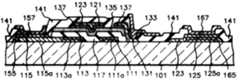
질화 실리콘이나 산화 실리콘과 같은 절연 물질을 상기 소스 전극(121), 소스 배선(123) 그리고, 드레인 전극(131)들이 형성된 기판 전면에 증착하여 보호막(141)을 형성한다. 그리고, 포토 리소그래피 법으로 상기 보호막(141) 일부를 제거하여 드레인 전극에는 콘택 홀(171)을 형성한다. 그리고, 소스 패드(125)와 게이트 패드(115)를 덮는 상기 보호막(141)의 일부를 제거하여 에는 소스 패드 콘택 홀(161)과 게이트 패드 콘택 홀(151)을 형성한다(제4e도).An insulating material such as silicon nitride or silicon oxide is deposited on the entire surface of the substrate on which the
그리고, ITO(Indium-Tin-Oxide)를 상기 보호막(141) 위에 전면 증착하고, 패턴하여 화소 전극(133), 소스 패드 연결 단자(167) 그리고, 게이트 패드 연결 단자(157)들을 형성한다. 상기 화소 전극(133)은 드레인 콘택 홀(171)을 통하여 드레인 전극(131)과 연결된다. 상기 소스 패드 연결 단자(167)는 소스 패드 콘택 홀(161)을 통하여 소스 패드(125)와 연결되며, 상기 게이트 패드 연결 단자(157)는 게이트 패드 콘택 홀(151)을 통하여 게이트 패드(115)와 연결된다(제4f도).Indium-tin-oxide (ITO) is deposited on the
여기에서는 게이트 패드 부분은 크롬, 몰리브덴, 탄탈 혹은, 주석을 포함하는 게이트 패드(115)와, 그 위에 크롬으로 이루어진 게이트 패드 중간 전극(155) 그리고, 보호막(141)에 형성된 게이트 패드 콘택 홀(151)을 통하여 상기 게이트 패드 중간전극(155)과 연결된 ITO로 이루어진 게이트 패드 연결 단자(157)로 형성되어 있다.The gate pad portion may include a
그리고, 소스 패드 부분 역시 크롬, 몰리브덴, 탄탈 혹은, 주석을 포함하는 소스 패드(125)와, 그 위에 크롬으로 이루어진 소스 패드 중간 전극(165) 그리고, 보호막에 형성된 소스 패드 콘택 홀(161)을 통하여 상기 소스 패드 중간 전극(165)과 연결된 ITO로 이루어진 소스 패드 연결 단자(167)로 형성되어 있다.The source pad portion may also include a
[실시예 2]Example 2
이번 실시예는 게이트 패드와 소스 패드 부분에 또 다른 구조를 갖는 경우이다. 평면 확대도인 제3도과, 절단선 Ⅳ-Ⅳ로 절단한 단면도인 제5도를 이용하여 설명한다.In this embodiment, the gate pad and the source pad have different structures. It demonstrates using FIG. 3 which is an enlarged plan view and FIG. 5 which is sectional drawing cut | disconnected by cut line IV-IV.
투명 기판(101) 위에 알루미늄을 포함하는 금속을 전면 증착한다. 포토 리소그래피 법을 사용하여 저 저항 게이트 전극(111a), 저 저항 게이트 배선(113a), 저 저항 게이트 패드(115a) 그리고, 저 저항 소스 패드(125a)를 형성된다. 저 저항 게이트 전극(111a)은 행렬 배열 방식으로 설계된 화소의 한쪽 구석에 형성된다. 그리고, 저 저항 게이트 배선(113a)은 열 방향으로 배열된 상기 저 저항 게이트 전극(111a)들을 연결하고 있다. 저 저항 게이트 패드(115a)는 상기 저 저항 게이트 배선(113a)의 끝단에 형성된다. 저 저항 소스 패드(125a)는 나중에 형성될 소스 배선(123)의 끝 부분에 형성된다(제3도, 제5a도).A metal including aluminum is deposited on the
상기 저 저항 게이트 전극(111a), 저 저항 게이트 배선(113a), 저 저항 게이트 패드(115a) 그리고, 저 저항 소스 패드(125a)가 형성된 기판 위에 크롬, 몰리브덴, 탄탈 혹은 주석 등을 전면 증착한다. 포토 리소그래피 법으로 패턴하여 상기 저 저항 게이틀 전극(111a)을 덮는 게이트 전극(111)을 형성한다. 그리고, 상기 저 저항 게이트 배선(113a)을 덮는 게이트 배선(113)과, 상기 저 저항 게이트 패드(115a)를 덮는 게이트 패드(115)를 형성한다. 그리고, 상기 저 저항 소스 패드(125a)를 덮는 소스 패드(125)를 형성한다(제5b도).Chrome, molybdenum, tantalum, or tin is deposited on the substrate on which the low
상기 게이트 전극(111), 게이트 배선(113), 게이트 패드(115) 그리고, 소스 패드(125)가 형성된 기판 위에 산화 실리콘 혹은 질화 실리콘과 같은 절연 물질을 전면 증착한다. 그리고, 차례로 진성 반도체 물질과 불순물이 포함된 반도체 물질을 연속증착한다. 포토 리소그래피 법으로 패턴하여 상기 절연 물질, 진성 반도체 물질 그리고, 불순물이 첨가된 반도체 물질을 식각하여 게이트 절연막(117), 반도체 층(135) 그리고, 불순물 반도체 층(137)을 형성한다. 상기 게이트 절연막(117)은 상기 소스배선(123)이 게이트 배선(113)과 전기적으로 접촉하지 않도록 하기 위한 것이다. 그러므로 게이트 절연막(117)은 게이트 배선(113)과 게이트 전극(111)을 덮거나, 소스배선(123)의 밑에 형성된다. 또한, 상기 반도체 층(135)과 불순물 반도체 층(137)은 상기 게이트 절연막(117)과 같은 형태로 상기 게이트 절연막 위에 형성된다(제3도, 제5c도).An insulating material such as silicon oxide or silicon nitride is deposited on the substrate on which the
상기 반도체 층(135)과 불순물 반도체 층(137)이 형성된 기판 위에 크롬이나 크롬 합금과 같은 금속을 전면 증착한다. 패턴하여 소스 전극(121), 소스 배선(123), 드레인 전극(131), 소스 패드 중간 전극(165) 그리고, 게이트 패드 중간 전극(155)을 형성한다. 상기 소스 전극(121)은 게이트 전극(111)을 중심으로 상기 드레인 전극(131)과 대향하고 있다. 그리고, 상기 소스 전극(121)과 드레인 전극(131)을 마스크로 계속 식각하여 소스 전극(121)과 드레인 전극(131) 사이에 존재하는 불순물 반도체 층(137)을 완전히 분리한다. 상기 소스 배선(123)은 열 방향으로 배열된 소스 전극들을 서로 연결하고 있다. 상기 소스 패드 중간 전극은 게이트 절연막(117)을 식각할 때 노출된 소스 패드(125)를 덮고 있으며, 상기 게이트 패드 중간 전극(155)은 게이트 절연막(117)을 식각할 때 노출된 게이트 패드(115)를 덮고 있다(제5d도).A metal such as chromium or a chromium alloy is deposited on the substrate on which the
상기 소스 전극(121), 소스 배선(123), 드레인 전극(131), 소스 패드 중간 전극(165) 그리고, 게이트 패드 중간 전극(155)들이 형성된 기판 전면에 질화 실리콘이나 산화 실리콘과 같은 절연 물질을 증착하여 보호막(141)을 형성한다. 포토 리소그래피 법으로 패턴하여 드레인 콘택 홀(171), 게이트 패드 콘택 홀(151) 그리고, 소스패드 콘택 홀(161)을 형성한다. 상기 드레인 콘택홀(171)은 드레인 전극 위에 증착된 보호막(141)의 일부를 식각하여 형성한다. 상기 게이트 패드 콘택 홀(181)은 게이트 패드 중간 전극(113)을 덮고 있는 보호막(141)의 일부를 식각하여 형성한다. 그리고, 소스 패드 콘택 홀(161)은 소스 패드 중간 전극(165)을 덮고 있는 보호막(141)의 일부를 식각하여 형성한다(제5e도).An insulating material such as silicon nitride or silicon oxide is formed on the entire surface of the substrate on which the
상기 보호막(141) 위에 ITO(Indium-Tin-Oxide)를 전면 증착하고, 패턴하여 화소전극(133), 게이트 패드 연결 단자(157) 그리고, 소스 패드 연결 단자(167)들을 형성한다. 상기 화소 전극(133)은 드레인 콘택 홀(171)을 통하여 드레인 전극(131)과 전기적으로 연결되어있다. 상기 게이트 패드 연결 단자(157)는 게이트 패드 콘택 홀(151)을 통하여 게이트 패드 중간 전극(155)과 전기적으로 연결된다. 상기 소스 패드 연결 단자(167)는 소스 패드 콘택 홀(161)을 통하여 소스 패드 중간 전극(165)과 전기적으로 연결되어 있다(제5f도).An ITO (Indium-Tin-Oxide) is deposited on the
본 실시 예에서도 게이트 패드 부분과 소스 패드 부분이 같은 형태를 이루고 있다. 즉, 게이트 패드 부분은 알루미늄을 포함하는 저 저항 게이트 패드(115a)와, 상기 저 저항 게이트 패드(115a)를 덮는 크롬, 몰리브덴, 탄탈 혹은, 주석을 포함하는 게이트 패드(115)와, 상기 게이트 패드(115) 위에 형성되 크롬을 포함하는 게이트 패드 중간 전극(115)과, 보호막(141)에 형성된 게이트 패드 콘택 홀(151)을 통하여 상기 게이트 패드 중간 전극(155)에 연결된 ITO로 이루어진 게이트 패드 연결 단자(157)로 이루어진 구조로 되어 있다. 마찬가지로 소스 패드 부분은 알루미늄을 포함하는 저 저항 소스 패드(125a)와, 상기 저 저항 소스 패드(125a)를 덮는 크롬, 몰리브덴, 탄탈 혹은, 주석을 포함하는 소스 패드(125)와, 상기 소스 패드(125)위에 형성된 크롬을 포함하는 소스 패드 중간 전극(165)과, 보호막(141)에 형성된 소스 패드 콘택 홀(161)을 통하여 상기 소스 패드 중간 전극(165)에 연결된 ITO로 이루어진 소스 패드 연결 단자(167)로 이루어진 구조로 되어 있다.In this embodiment, the gate pad portion and the source pad portion have the same shape. That is, the gate pad portion may include a low
본 발명에서는 게이트 전극, 게이트 배선, 게이트 패드 및 소스 패드를 알루미늄을 포함하는 금속으로 형성하는 과정에서 알루미늄 표면에 힐락이 발생하는 것을 막기 위해서 사용하는 양극 산화 공정을 따르지 않고, 크롬, 몰리브덴, 탄탈 혹은, 주석과 같은 금속으로 보호를 하였다. 그리고, 게이트 절연막을 패턴하여 게이트 패드와 소스 패드를 노출시키고, 보호막에 콘택 홀을 형성하여 패드부의 연결 단자를 형성하였다. 따라서, 능동 매트릭스 액정 기판을 제조할 때 사용하는 마스크 공정 수를 줄일 수 있었다. 그럼으로써, 제조 공정이 단순해지고, 마스크 정렬에서 발생하는 오차의 누적을 줄일 수 있었다. 따라서, 액정 표시 장치의 제조 수율과 액정 표시장치의 품질을 결정하는 화질이 더욱 향상되었다. 더욱이 제조에 소요되는 시간이 절감되어 제조 비용이 절감되는 효과도 얻을 수 있었다.In the present invention, chromium, molybdenum, tantalum or the like is not used in the process of forming the gate electrode, the gate wiring, the gate pad, and the source pad from a metal containing aluminum, without following the anodization process used to prevent the occurrence of hillock on the aluminum surface. And protected with a metal such as tin. The gate insulating layer was patterned to expose the gate pad and the source pad, and contact holes were formed in the passivation layer to form connection terminals of the pad portion. Therefore, the number of mask processes used when manufacturing an active matrix liquid crystal substrate can be reduced. This simplifies the manufacturing process and reduces the accumulation of errors in mask alignment. Therefore, the image quality which determines the manufacturing yield of a liquid crystal display device and the quality of a liquid crystal display device further improved. In addition, the time required for manufacturing was reduced, thereby reducing the manufacturing cost.
Claims (26)
Translated fromKoreanPriority Applications (1)
| Application Number | Priority Date | Filing Date | Title |
|---|---|---|---|
| KR1019970004290AKR100235594B1 (en) | 1997-02-13 | 1997-02-13 | Liquid crystal display and method for manufacturing the same |
Applications Claiming Priority (1)
| Application Number | Priority Date | Filing Date | Title |
|---|---|---|---|
| KR1019970004290AKR100235594B1 (en) | 1997-02-13 | 1997-02-13 | Liquid crystal display and method for manufacturing the same |
Publications (2)
| Publication Number | Publication Date |
|---|---|
| KR19980067921A KR19980067921A (en) | 1998-10-15 |
| KR100235594B1true KR100235594B1 (en) | 1999-12-15 |
Family
ID=19496928
Family Applications (1)
| Application Number | Title | Priority Date | Filing Date |
|---|---|---|---|
| KR1019970004290AExpired - LifetimeKR100235594B1 (en) | 1997-02-13 | 1997-02-13 | Liquid crystal display and method for manufacturing the same |
Country Status (1)
| Country | Link |
|---|---|
| KR (1) | KR100235594B1 (en) |
Families Citing this family (4)
| Publication number | Priority date | Publication date | Assignee | Title |
|---|---|---|---|---|
| KR100471765B1 (en)* | 1997-07-11 | 2005-07-18 | 삼성전자주식회사 | Thin film transistor substrate with single film gate line and manufacturing method |
| KR100580400B1 (en)* | 1999-01-15 | 2006-05-15 | 삼성전자주식회사 | Thin film transistor substrate for liquid crystal display device and manufacturing method thereof |
| KR100777698B1 (en)* | 2001-04-17 | 2007-11-21 | 삼성전자주식회사 | Thin film transistor substrate for liquid crystal display device and manufacturing method thereof |
| KR100527086B1 (en)* | 2001-09-05 | 2005-11-09 | 비오이 하이디스 테크놀로지 주식회사 | Method for manufacturing liquid crystal display device |
- 1997
- 1997-02-13KRKR1019970004290Apatent/KR100235594B1/ennot_activeExpired - Lifetime
Also Published As
| Publication number | Publication date |
|---|---|
| KR19980067921A (en) | 1998-10-15 |
Similar Documents
| Publication | Publication Date | Title |
|---|---|---|
| KR100229613B1 (en) | Liquid Crystal Display and Manufacturing Method | |
| KR100244447B1 (en) | Liquid crystal display device and manufacturing method of liquid crystal display device | |
| US6172733B1 (en) | Liquid crystal display including conductive layer passing through multiple layers and method of manufacturing same | |
| US6373546B1 (en) | Structure of a liquid crystal display and the method of manufacturing the same | |
| KR100255592B1 (en) | Liquid crystal display device and its manufacturing method | |
| KR100271038B1 (en) | A manufacturing method of shorting bar probing and electrical state and a structure of an lcd comprising the shorting bar | |
| KR100262953B1 (en) | Liquid crystal display device and manufacturing method of liquid crystal display device | |
| US6184948B1 (en) | Liquid crystal display device having a plurality of error detecting shorting bars and a method of manufacturing the same | |
| US20110025939A1 (en) | Liquid crystal display device and its manufacturing method | |
| KR100482167B1 (en) | LCD and its manufacturing method | |
| KR100235594B1 (en) | Liquid crystal display and method for manufacturing the same | |
| KR20000019504A (en) | Method for manufacturing lcd | |
| KR100248256B1 (en) | The structure of lcd and its fabrication method | |
| KR100235593B1 (en) | Liquid crystal display and method for manufacturing the same | |
| KR100252307B1 (en) | Manufacturing method of liquid crystal display device and structure of liquid crystal display device by the method | |
| KR100243813B1 (en) | Liquid crystal display and method for manufacturing the same | |
| KR100514764B1 (en) | Liquid crystal display device and the method for manufaturing the same | |
| GB2347267A (en) | A liquid crystal display contact pad | |
| KR20050069038A (en) | Method of fabricating liquid crystal display |
Legal Events
| Date | Code | Title | Description |
|---|---|---|---|
| A201 | Request for examination | ||
| PA0109 | Patent application | Patent event code:PA01091R01D Comment text:Patent Application Patent event date:19970213 | |
| PA0201 | Request for examination | Patent event code:PA02012R01D Patent event date:19970213 Comment text:Request for Examination of Application | |
| PG1501 | Laying open of application | ||
| E701 | Decision to grant or registration of patent right | ||
| PE0701 | Decision of registration | Patent event code:PE07011S01D Comment text:Decision to Grant Registration Patent event date:19990628 | |
| N231 | Notification of change of applicant | ||
| PN2301 | Change of applicant | Patent event date:19990903 Comment text:Notification of Change of Applicant Patent event code:PN23011R01D | |
| GRNT | Written decision to grant | ||
| PR0701 | Registration of establishment | Comment text:Registration of Establishment Patent event date:19990927 Patent event code:PR07011E01D | |
| PR1002 | Payment of registration fee | Payment date:19990928 End annual number:3 Start annual number:1 | |
| PG1601 | Publication of registration | ||
| PR1001 | Payment of annual fee | Payment date:20020624 Start annual number:4 End annual number:4 | |
| PR1001 | Payment of annual fee | Payment date:20030701 Start annual number:5 End annual number:5 | |
| PR1001 | Payment of annual fee | Payment date:20040629 Start annual number:6 End annual number:6 | |
| PR1001 | Payment of annual fee | Payment date:20050627 Start annual number:7 End annual number:7 | |
| PR1001 | Payment of annual fee | Payment date:20060629 Start annual number:8 End annual number:8 | |
| PR1001 | Payment of annual fee | Payment date:20070702 Start annual number:9 End annual number:9 | |
| PR1001 | Payment of annual fee | Payment date:20080701 Start annual number:10 End annual number:10 | |
| PR1001 | Payment of annual fee | Payment date:20090622 Start annual number:11 End annual number:11 | |
| PR1001 | Payment of annual fee | Payment date:20100621 Start annual number:12 End annual number:12 | |
| PR1001 | Payment of annual fee | Payment date:20110615 Start annual number:13 End annual number:13 | |
| PR1001 | Payment of annual fee | Payment date:20120628 Start annual number:14 End annual number:14 | |
| FPAY | Annual fee payment | Payment date:20130619 Year of fee payment:15 | |
| PR1001 | Payment of annual fee | Payment date:20130619 Start annual number:15 End annual number:15 | |
| FPAY | Annual fee payment | Payment date:20140630 Year of fee payment:16 | |
| PR1001 | Payment of annual fee | Payment date:20140630 Start annual number:16 End annual number:16 | |
| FPAY | Annual fee payment | Payment date:20150818 Year of fee payment:17 | |
| PR1001 | Payment of annual fee | Payment date:20150818 Start annual number:17 End annual number:17 | |
| FPAY | Annual fee payment | Payment date:20160816 Year of fee payment:18 | |
| PR1001 | Payment of annual fee | Payment date:20160816 Start annual number:18 End annual number:18 | |
| EXPY | Expiration of term | ||
| PC1801 | Expiration of term |