KR100235589B1 - Driving Method of Thin Film Transistor Liquid Crystal Display - Google Patents
Driving Method of Thin Film Transistor Liquid Crystal DisplayDownload PDFInfo
- Publication number
- KR100235589B1 KR100235589B1KR1019970000293AKR19970000293AKR100235589B1KR 100235589 B1KR100235589 B1KR 100235589B1KR 1019970000293 AKR1019970000293 AKR 1019970000293AKR 19970000293 AKR19970000293 AKR 19970000293AKR 100235589 B1KR100235589 B1KR 100235589B1
- Authority
- KR
- South Korea
- Prior art keywords
- drain
- source
- transistor
- contact
- gate
- Prior art date
- Legal status (The legal status is an assumption and is not a legal conclusion. Google has not performed a legal analysis and makes no representation as to the accuracy of the status listed.)
- Expired - Lifetime
Links
Images


Classifications
- G—PHYSICS
- G11—INFORMATION STORAGE
- G11C—STATIC STORES
- G11C19/00—Digital stores in which the information is moved stepwise, e.g. shift registers
- G11C19/18—Digital stores in which the information is moved stepwise, e.g. shift registers using capacitors as main elements of the stages
- G11C19/182—Digital stores in which the information is moved stepwise, e.g. shift registers using capacitors as main elements of the stages in combination with semiconductor elements, e.g. bipolar transistors, diodes
- G11C19/184—Digital stores in which the information is moved stepwise, e.g. shift registers using capacitors as main elements of the stages in combination with semiconductor elements, e.g. bipolar transistors, diodes with field-effect transistors, e.g. MOS-FET
- G—PHYSICS
- G09—EDUCATION; CRYPTOGRAPHY; DISPLAY; ADVERTISING; SEALS
- G09G—ARRANGEMENTS OR CIRCUITS FOR CONTROL OF INDICATING DEVICES USING STATIC MEANS TO PRESENT VARIABLE INFORMATION
- G09G3/00—Control arrangements or circuits, of interest only in connection with visual indicators other than cathode-ray tubes
- G09G3/20—Control arrangements or circuits, of interest only in connection with visual indicators other than cathode-ray tubes for presentation of an assembly of a number of characters, e.g. a page, by composing the assembly by combination of individual elements arranged in a matrix no fixed position being assigned to or needed to be assigned to the individual characters or partial characters
- G09G3/34—Control arrangements or circuits, of interest only in connection with visual indicators other than cathode-ray tubes for presentation of an assembly of a number of characters, e.g. a page, by composing the assembly by combination of individual elements arranged in a matrix no fixed position being assigned to or needed to be assigned to the individual characters or partial characters by control of light from an independent source
- G09G3/36—Control arrangements or circuits, of interest only in connection with visual indicators other than cathode-ray tubes for presentation of an assembly of a number of characters, e.g. a page, by composing the assembly by combination of individual elements arranged in a matrix no fixed position being assigned to or needed to be assigned to the individual characters or partial characters by control of light from an independent source using liquid crystals
- G09G3/3611—Control of matrices with row and column drivers
- G09G3/3674—Details of drivers for scan electrodes
- G09G3/3677—Details of drivers for scan electrodes suitable for active matrices only
- G—PHYSICS
- G09—EDUCATION; CRYPTOGRAPHY; DISPLAY; ADVERTISING; SEALS
- G09G—ARRANGEMENTS OR CIRCUITS FOR CONTROL OF INDICATING DEVICES USING STATIC MEANS TO PRESENT VARIABLE INFORMATION
- G09G2300/00—Aspects of the constitution of display devices
- G09G2300/04—Structural and physical details of display devices
- G09G2300/0404—Matrix technologies
- G09G2300/0408—Integration of the drivers onto the display substrate
- G—PHYSICS
- G09—EDUCATION; CRYPTOGRAPHY; DISPLAY; ADVERTISING; SEALS
- G09G—ARRANGEMENTS OR CIRCUITS FOR CONTROL OF INDICATING DEVICES USING STATIC MEANS TO PRESENT VARIABLE INFORMATION
- G09G2310/00—Command of the display device
- G09G2310/02—Addressing, scanning or driving the display screen or processing steps related thereto
- G09G2310/0202—Addressing of scan or signal lines
- G09G2310/0205—Simultaneous scanning of several lines in flat panels
- G—PHYSICS
- G09—EDUCATION; CRYPTOGRAPHY; DISPLAY; ADVERTISING; SEALS
- G09G—ARRANGEMENTS OR CIRCUITS FOR CONTROL OF INDICATING DEVICES USING STATIC MEANS TO PRESENT VARIABLE INFORMATION
- G09G2310/00—Command of the display device
- G09G2310/02—Addressing, scanning or driving the display screen or processing steps related thereto
- G09G2310/0264—Details of driving circuits
- G09G2310/0281—Arrangement of scan or data electrode driver circuits at the periphery of a panel not inherent to a split matrix structure
Landscapes
- Engineering & Computer Science (AREA)
- Microelectronics & Electronic Packaging (AREA)
- Chemical & Material Sciences (AREA)
- Crystallography & Structural Chemistry (AREA)
- Physics & Mathematics (AREA)
- Computer Hardware Design (AREA)
- General Physics & Mathematics (AREA)
- Theoretical Computer Science (AREA)
- Power Engineering (AREA)
- Liquid Crystal Display Device Control (AREA)
- Liquid Crystal (AREA)
- Control Of Indicators Other Than Cathode Ray Tubes (AREA)
Abstract
Translated fromKoreanDescription
Translated fromKorean본 발명은 액정표시장치를 구동하는 데 사용되는 주사선선택구동회로의 구조를 간단히 하고, 아몰퍼스 실리콘(이하 a-Si)으로 제작하여 액정패널과 주사선구동회로를 동시에 제조함으로써 안정적인 주사신호를 인가하는 주사선선택구동회로의 제조단가를 절감시키는 데에 목적이 있다.The present invention simplifies the structure of the scan line selection driver circuit used to drive a liquid crystal display, and is made of amorphous silicon (hereinafter referred to as a-Si) to simultaneously manufacture a liquid crystal panel and a scan line driver circuit, thereby applying a stable scan signal. The purpose is to reduce the manufacturing cost of the selective drive circuit.
현재 표시장치로써 가장 많이 사용되고 있는 CRT 브라운관은 색상구현이 쉽고, 동작속도가 빨라 TV와 컴퓨터모니터를 포함한 디스플레이 장치로서 각광을 받아 왔다. 그러나, CRT 브라운관은 전자총과 화면 사이의 거리를 어느정도 확보해야 하는 구조적 특성으로 인하여 두께가 두꺼울 뿐만 아니라, 전력소비가 크고, 게다가 무게도 상당히 무거워 휴대성이 떨어지는 단점이 있다.CRT CRT, which is the most widely used display device, has been spotlighted as a display device including TV and computer monitor because of its easy color and fast operation speed. However, CRT CRTs are not only thick, due to the structural characteristics of securing a certain distance between the electron gun and the screen, but also have high power consumption, and are also very heavy.
상술한 CRT 브라운관의 단점을 극복하고자 여러 가지 다양한 표시장치가 고안되고 있는데, 그 중 가장 실용화 되어 있는 장치가 바로 액정표시장치이다.In order to overcome the disadvantages of the CRT CRT described above, a variety of display devices have been devised, the most practical of which is a liquid crystal display device.
액정표시장치는 CRT 브라운관에 비해 화면이 어둡고 동작속도가 다소 느리지만, 전자총과 같은 장치를 갖추지 않아도 각각의 화소를 평면 상에서 주사되는 신호에 따라 동작시킬 수 있으므로, 얇은 두께로 제작될 수 있어 장차 벽걸이 TV와 같은 초박형 표시장치로 사용될 수 있다. 뿐만 아니라, 액정표시장치는 무게가 가볍고, 전력소비도 CRT 브라운관에 비해 상당히 적어 배터리로 동작하는 노트북 컴퓨터의 디스플레이로 사용되는 등, 휴대용 표시장치로서 가장 적합하다는 평도 받고 있다.LCD displays have a darker screen and somewhat slower operating speeds than CRT CRTs.However, even without a device such as an electron gun, each pixel can be operated according to the signal scanned on a plane. It can be used as an ultra-thin display such as a TV. In addition, the liquid crystal display device has a reputation for being the most suitable as a portable display device, such as being used as a display of a battery-operated notebook computer because it is light in weight and consumes significantly less than a CRT CRT.
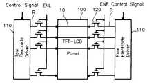
상술한 바와 같이 차세대 표시장치로서 각광받고 있는 액정표시장치는 도1과 같이 액정패널과 상기 액정패널을 구동할 수 있는 주사선구동회로 및 신호선구동회로로 구성되어 있다. 그런데, 상기 액정패널은 기판에 복수개의 주사선(11)과 복수개의 신호선(12)이 매트릭스형태로 교차하여 설치되어 있고, 그 교차부에는 박막트랜지스터(14)(이하 TFT라고 한다.)와 화소가 설치된 구조로 되어 있다. 그리고, 상기 주사선선택구동회로는 상기 박막트랜지스터의 게이트에 온(on)신호를 인가하는 주사신호를 상기 주사선에 순차적으로 인가하고, 상기 신호선구동회로는 상기 주사신호에 의해 구동된 TFT를 통하여 영상신호가 화소에 전달될 수 있도록 영상신호를 신호선에 인가한다. 상기 액정표시장치는 상기 주사선선택구동회로에서 주사신호를 상기 액정패널의 주사선에 순차적으로 인가해서 상기 주사신호를 인가받은 상기 주사선에 연결된 모든 TFT가 도통하게(on) 되면, 상기 액정패널의 신호선에 인가된 신호가 상기 도통된 TFT의 소스와 드레인을 통하여 화소로 전달되는 원리로 작동한다.As described above, the liquid crystal display device, which is in the spotlight as a next generation display device, is composed of a liquid crystal panel, a scan line driver circuit and a signal line driver circuit capable of driving the liquid crystal panel as shown in FIG. By the way, in the liquid crystal panel, a plurality of
상기 액정표시장치에서 사용되는 종래의 주사선선택구동회로는 도2와 같이 쉬프트입력신호를 인가받는 SIn단자에 접속된 게이트전극과 제1공통전압 Vss1에 연결된 드레인전극으로 이루어진 M2트랜지스터와, 상기 SIn단자에 접속된 게이트전극과 두 번째 클럭신호를 인가받는 S2o단자에 연결된 소스전극으로 이루어진 M4트랜지스터, 첫 번째 클럭신호를 인가받는 S1o단자에 접속된 게이트와 외부전압 Vcc와 연결된 소스전극과 상기 M2트랜지스터의 소스전극에 연결된 드레인전극으로 이루어진 M1트랜지스터와 그리고, 상기 M1의 드레인전극과 상기 M2의 소스전극 사이의 접점 a2에 게이트전극이 접속된 M3, M5, M7의 세 개의 트랜지스터와, 상기 M4의 드레인전극에 접속된 게이트전극와 세 번째 클럭신호 S3o신호에 소스전극이 연결된 구조로 이루어진 M6트랜지스터와, 상기 SIn 단자에 접속된 게이트와 상기 Vss1에 연결된 소스전극으로 이루어진 M11트랜지스터와, 상기 S1o의 2배의 주기를 갖는 네 번째 클럭신호 S4가 접속된 게이트와 인접한 열에 위치한 구동회로의 출력에 연결된 소스전극으로 이루어진 M9트랜지스터와, 상기 M9의 드레인전극에 연결된 게이트전극과 상기 M11트랜지스터의 드레인전극에 연결된 소스전극으로 이루어진 M10트랜지스터와, 상기 M10의 소스전극과 상기 M11의 드레인전극 사이의 접점 d2에 연결된 게이트전극과 상기 M7의 소스전극과 상기 M6의 드레인전극 사이의 접점에 연결된 드레인전극이 상기 M7의 드레인전극과 제2공통전압 Vss에 공통으로 접속된 M8트랜지스터가 설치된 홀수번째 스테이지와; 상기 구동회로의 출력에 연결되어 쉬프트입력신호를 인가받는 SIn+1단자에 접속된 게이트전극과 제1공통전압 Vss1에 연결된 드레인전극으로 이루어진 M2트랜지스터와, 상기 SIn+1단자에 접속된 게이트전극과 두 번째 클럭신호를 인가받는 S2e단자에 연결된 소스전극으로 이루어진 M4트랜지스터, 첫 번째 클럭신호를 인가받는 S1e단자에 접속된 게이트와 외부전압 Vcc와 연결된 소스전극과 상기 M2트랜지스터의 소스전극에 연결된 드레인전극으로 이루어진 M1트랜지스터와 그리고, 상기 M1의 드레인전극과 상기 M2의 소스전극 사이의 접점 a3에 게이트전극이 접속된 M3, M5, M7의 세 개의 트랜지스터와, 상기 M4의 드레인전극에 접속된 게이트전극와 세 번째 클럭신호 S3e신호에 소스전극이 연결된 구조로 이루어진 M6트랜지스터와, 상기 SIn+1 단자에 접속된 게이트와 상기 Vss1에 연결된 소스전극으로 이루어진 M11트랜지스터와, 상기 S1e의 2배의 주기를 갖는 네 번째 클럭신호 S4가 접속된 게이트와 인접한 열에 위치한 구동회로의 출력에 연결된 소스전극으로 이루어진 M9트랜지스터와, 상기 M9의 드레인전극에 연결된 게이트전극과 상기 M11트랜지스터의 드레인전극에 연결된 소스전극으로 이루어진 M10트랜지스터와, 상기 M10의 소스전극과 상기 M11의 드레인전극 사이의 접점 d3에 연결된 게이트전극과 상기 M7의 소스전극과 상기 M6의 드레인전극 사이의 접점에 연결된 드레인전극이 상기 M7의 드레인전극과 제2공통전압 Vss에 공통으로 접속된 M8트랜지스터가 설치된 짝수번째 스테이지가 여러 개 직렬로 연결된 구조로 되어 있다.The conventional scan line selection driver circuit used in the liquid crystal display includes an M2 transistor including a gate electrode connected to the SIn terminal receiving the shift input signal and a drain electrode connected to the first common voltage Vss1, as shown in FIG. A M4 transistor comprising a gate electrode connected to the terminal and a source electrode connected to an S2o terminal receiving the second clock signal, a gate connected to the S1o terminal receiving the first clock signal, a source electrode connected to an external voltage Vcc, and the M2 transistor of the M2 transistor. M1 transistor consisting of a drain electrode connected to a source electrode, three transistors of M3, M5 and M7 having a gate electrode connected to a contact a2 between the drain electrode of M1 and the source electrode of M2, and the drain electrode of M4. M6 transistor having a structure in which a source electrode is connected to a gate electrode connected to the third clock signal S3o signal And a source connected to an output of a driving circuit positioned in a column adjacent to the gate to which the M11 transistor including a gate connected to the SIn terminal and a source electrode connected to the Vss1, and a fourth clock signal S4 having a period twice as long as S1o is connected. An M10 transistor comprising an electrode, a gate electrode connected to the drain electrode of the M9 and a source electrode connected to the drain electrode of the M11 transistor, and a contact d2 between the source electrode of the M10 and the drain electrode of the M11. An odd-numbered stage provided with an M8 transistor in which a drain electrode connected to a gate electrode and a contact between the source electrode of M7 and the drain electrode of M6 is commonly connected to the drain electrode of M7 and a second common voltage Vss; A M2 transistor comprising a gate electrode connected to an output of the driving circuit and receiving a shift input signal and a drain electrode connected to a first common voltage Vss1, and a gate electrode connected to the SIn + 1 terminal; M4 transistor comprising a source electrode connected to the S2e terminal receiving the second clock signal, a gate connected to the S1e terminal receiving the first clock signal, a source electrode connected to an external voltage Vcc, and a drain electrode connected to the source electrode of the M2 transistor A transistor of M1, three transistors of M3, M5, and M7 having a gate electrode connected to the contact a3 between the drain electrode of M1 and the source electrode of M2; and a gate electrode connected to the drain electrode of M4. A M6 transistor having a structure in which a source electrode is connected to the first clock signal S3e signal, a gate connected to the SIn + 1 terminal, An M11 transistor comprising a source electrode connected to a predetermined Vss1, an M9 transistor consisting of a source electrode connected to an output of a driving circuit located in a column adjacent to a gate to which a fourth clock signal S4 having a period twice the S1e is connected, and the M9 A M10 transistor comprising a gate electrode connected to the drain electrode of the transistor and a source electrode connected to the drain electrode of the M11 transistor, a gate electrode connected to the contact point d3 between the source electrode of the M10 and the drain electrode of the M11, and the source electrode of the M7; A plurality of even-numbered stages in which a drain electrode connected to a contact between the drain electrodes of the M6 is connected to the drain electrode of the M7 and the second common voltage Vss are connected in series are connected in series.
상기 주사선선택구동회로의 동작은, 상기 액정표시장치에 가해지는 수평주사기간의 2배 주기를 갖고 액정표시장치에서 홀수번째의 열에 위치한 주사선에 출력신호를 인가하는 홀수스테이지의 클럭단자로 보내지는 세 개의 클럭신호 S1o, S2o, S3o와 상기 액정표시장치의 짝수번째의 열에 위치한 주사선에 출력신호를 인가하는 짝수스테이지의 클럭단자로 보내지는 세 개의 클럭신호 S1e, S2e, S3e 그리고, 수평주사기간과 동일한 주기를 갖는 클럭신호 S4신호가 인가됨으로써 이루어진다. 상기 홀수스테이지는 상기 S1o, S2o, S3o과 입력단자 SIn에 인가되는 쉬프트신호에 의해 출력되는 Ro을 상기 액정패널의 홀수번째 열에 위치한 주사선에 차례로 인가하고, 짝수스테이지는 상기 S1e, S2e, S3e와 입력단자 SIn+1에 인가되는 쉬프트신호에 의해 출력되는 Re를 상기 액정패널의 짝수번째 열에 위치한 주사선에 차례로 인가한다. 또한, n번째 열의 출력선 Rn은 상기 주사선에 인가되면서, 동시에 인접한 n+1번째 열의 상기 주사선에 상기 출력신호를 인가하는 상기 스테이지의 상기 입력단자 SIn+1에 쉬프트신호로서 인가된다. 그러나, 첫 번째 열에 위치한 주사선으로 출력신호를 인가하는 상기 구동회로의 입력단자에는 따로 쉬프트클럭신호를 인가한다.The operation of the scan line selection driver circuit has three cycles of the horizontal scanning period applied to the liquid crystal display device and is sent to the clock terminal of the odd stage for applying an output signal to the scan line located in the odd column of the liquid crystal display device. Clock signals S1o, S2o, S3o and three clock signals S1e, S2e, S3e sent to the clock terminals of an even stage for applying an output signal to the scan lines located in the even-numbered columns of the liquid crystal display, and the same as the horizontal scanning period. This is achieved by applying a clock signal S4 having a period. The odd stage sequentially applies Ro, which is output by the shift signal applied to the S1o, S2o, and S3o and the input terminal SIn, to the scan line located in the odd-numbered column of the liquid crystal panel, and the even stage is input to the S1e, S2e, and S3e. Re, which is output by the shift signal applied to the terminal SIn + 1, is sequentially applied to the scan lines positioned in the even columns of the liquid crystal panel. The output line Rn in the nth column is applied as the shift signal to the input terminal SIn + 1 of the stage which simultaneously applies the output signal to the scan line in the n + 1th column while being applied to the scan line. However, a shift clock signal is separately applied to an input terminal of the driving circuit which applies an output signal to the scan line located in the first column.
상기 주사선선택구동회로의 동작을 도2의 회로도와 도3의 파형도를 참조로 설명하면 다음과 같다.The operation of the scan line selection driving circuit will be described with reference to the circuit diagram of FIG. 2 and the waveform diagram of FIG. 3.
먼저, 첫 번째 스테이지의 입력단자에 SIn을 하이(high)로 인가하여 M2와 M4를 도통시킨다.(t2) 그러나, 이 때에는 S1o와 S2o가 하이(high)로 인가되지 않았으므로, 상기 M2와 M4의 소스와 드레인에는 전압이 인가되지 않으므로, M3와 M5 그리고, M7은 도통되지 않는다. 또한, 상기 M4가 도통되지 않으므로, M6도 도통되지 않는다.First, SIn is applied to the input terminal of the first stage high to conduct M2 and M4. (T2) However, at this time, since S1o and S2o are not applied high, the M2 and M4 Since no voltage is applied to the source and the drain of M3, M5 and M7 are not conducted. In addition, since M4 is not conductive, M6 is also not conductive.
상기 SIn이 하이(high)로 된 후, 수평주사주기에 의하여 S1o가 상기 첫 번째 열의 스테이지에 인가되어 M1을 도통시킨다.(t3) 이 때, M1과 M2 사이의 접점 a1과 연결된 M3, M5, M7이 모두 도통된다. 그러나, M5는 M4가 도통되지 않은 상태이므로 전압이 인가되지 않고, M7은 M6이 도통되지 않은 상태이므로 전압이 인가되지 않는다.After SIn becomes high, S1o is applied to the stage of the first row by a horizontal scanning period to conduct M1. (T3) At this time, M3, M5, connected to the contact a1 between M1 and M2, M7 is all conducting. However, no voltage is applied to M5 because M4 is not conductive, and no voltage is applied to M7 because M6 is not conductive.
상기 S1o가 로우(low)로 떨어지기 전에 S2o가 하이(high)로 인가되어 M4와 M5 사이의 접점 b1을 통해 M6를 도통시킨다.(t4) 이 때, M5를 통해 인가된 S2o전압이 상기 SIn에 의해 도통된 M11을 통해 M8을 도통시킨다.Before S1o falls low, S2o is applied high to conduct M6 through contact b1 between M4 and M5. (T4) At this time, the S2o voltage applied through M5 is applied to the SIn. Conducts M8 through M11 conducted by.
상기 S1o가 로(low)로 떨어지면 상기 M1이 단절되고, a1에 게이트가 연결되어 있는 M5와 M7가 단절된다.(t5)When S1o falls to low, M1 is disconnected, and M5 and M7, whose gates are connected to a1, are disconnected. (T5)
상기 S2o가 하이(high)로 유지된 상태에서 상기 S1o가 로(low)로 떨어진 후, 약간의 시간차를 두고 S3o가 하이(high)로 인가된다.(t6) 그러면, 이 때, 상기 S2o에 의해 도통된 M6을 통해 S3o가 Rn단자를 통해 주사선으로 인가된다. 동시에 상기 S3o는 인접한 다음 스테이지의 쉬프트신호로서 상기 다음 스테이지의 M2 트랜지스터의 게이트에 인가된다.After S1o falls low with S2o held high, S3o is applied high with a slight time difference. (T6) At this time, by S2o Through conduction M6, S3o is applied to the scan line through the Rn terminal. At the same time, the S3o is applied to the gate of the M2 transistor of the next stage as a shift signal of the next adjacent stage.
상기 다음 스테이지의 S1e가 하이(high)로 되면, 상기 SIn이 로(low)로 떨어지게 된다. 이 때, M2와 M4 그리고, M11이 단절된다.(t7) 그리고, 다음 스테이지가 상술한 전단계 스테이지의 동작을 반복한다.When S1e of the next stage becomes high, the SIn falls to low. At this time, M2, M4 and M11 are disconnected. (T7) Then, the next stage repeats the operation of the preceding stage.
액정표시장치에 있어서 최근의 기술동향을 보면, 과거에는 액정패널과 주변의 구동회로를 별개로 제조하여 리드선이나 필름으로 접착시켜 패키지화하는 방식이 주류를 이루었으나, 미세가공기술이 발전할수록 제품의 제조단가를 낮추기 위해 액정패널 위에 주변의 구동회로를 직접 실장시키는 기술이 연구되고 있다. 그런데, 상기 종래의 주사선선택구동회로는 액정패널 위에 직접 실장시키기에는 구조가 복잡하고 외부와 연결되는 리드선이 많아 제조가 힘들고 수율도 떨어진다.In recent years, in the LCD technology, in the past, a liquid crystal panel and a peripheral driving circuit were separately manufactured and bonded and packaged by a lead wire or a film. In order to reduce the unit cost, a technology for directly mounting peripheral driving circuits on a liquid crystal panel has been studied. However, the conventional scanning line selection driving circuit has a complicated structure and a large number of lead wires connected to the outside to mount directly on the liquid crystal panel, which makes manufacturing difficult and yields low.
또, 클럭신호가 표시장치의 수평주기의 하이(high)시간보다 조금 늦은 시간차를 두고 하이(high)로 변환되는데, 이것은 상기 주사선선택구동회로에서 사용되는 트랜지스터를 동작속도가 다소 느린 a-Si을 사용하기 때문에 a-Si이 충분히 반응할 시간을 확보하기 위해 설정한 한계이다. 즉, 회로기판의 반도체에 따라 상기 주기와 시간차를 적절히 조절하여 신호를 인가하는 것이 종래 발명의 중요한 요소인데, 바로 이런 점으로 인해 상기 종래의 주사선선택구동회로는 동작의 정확한 제어가 힘들다는 단점이 부각된다. 특히, 동작속도가 a-Si보다 빠른 폴리 실리콘(poly-Si)으로 상기 주사선선택구동회로를 제조하면, 정확한 동작을 기대하기 어렵다.In addition, the clock signal is converted to high with a time delay slightly higher than the high time of the horizontal period of the display device. This means that the transistor used in the scan line select driver circuit is a-Si whose operating speed is rather slow. This is the limit set in order to secure time for a-Si to react sufficiently. That is, it is an important element of the present invention to apply a signal by appropriately adjusting the period and time difference according to the semiconductor of the circuit board, which is a disadvantage that the precise control of the operation of the conventional scan line selection driving circuit is difficult. It is highlighted. In particular, when the scan line selection driving circuit is manufactured from poly-Si (poly-Si) whose operating speed is higher than that of a-Si, it is difficult to expect accurate operation.
그리고, 종래의 주사선선택구동회로에서 인가되는 동작파형의 특징은 순차적으로 인가되는 클럭신호 S1과 S2, S3의 하이(high)영역이 서로 조금씩 겹치도록 되어 있다는 점이다. 이것은 상기 S3 신호의 하이(high)시간이 구동신호와 쉬프트신호에 상당한 영향을 미치기 때문인데, 이로 인해 각 스테이지에서 거의 모든 TFT가 동시에 도통(on)되는 시간이 존재하여 상기 주사선선택구동회로에 형성된 TFT에 상당한 부하가 걸리게 된다.The characteristic of the operation waveform applied in the conventional scan line selection driver circuit is that the high regions of the clock signals S1, S2, and S3, which are sequentially applied, overlap each other little by little. This is because the high time of the S3 signal has a significant influence on the driving signal and the shift signal. As a result, there is a time that almost all the TFTs are turned on at the same time in each stage, thereby forming the scan line selection driving circuit. Substantial load is placed on the TFT.
도1은 일반적인 액정표시장치에서 액정패널과 주사선구동회로 및 신호선구동회로를 개략적으로 나타낸 도면이다.1 is a view schematically showing a liquid crystal panel, a scan line driver circuit, and a signal line driver circuit in a general liquid crystal display device.
도2는 종래의 주사선선택구동회로를 나타낸 회로도이다.2 is a circuit diagram showing a conventional scanning line selection driving circuit.
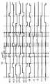
도3은 종래의 주사선선택구동회로의 동작을 나타낸 파형도이다.3 is a waveform diagram showing the operation of a conventional scanning line selection driving circuit.
도4는 본 발명의 주사선선택구동회로에서 단위 스테이지를 나타낸 회로도이다.4 is a circuit diagram showing a unit stage in the scan line selection drive circuit of the present invention.
도5는 본 발명의 주사선선택구동회로의 각 스테이지가 직렬로 연결된 구조를 나타낸 도면이다.5 is a view showing a structure in which each stage of the scan line selection driving circuit of the present invention is connected in series.
도6은 본 발명의 주사선선택구동회로의 동작을 나타낸 파형도이다.Fig. 6 is a waveform diagram showing the operation of the scan line selection driver circuit of the present invention.
도7은 본 발명의 주사선선택구동회로에서 단위 스테이지를 나타낸 또다른 회로도이다.7 is another circuit diagram showing a unit stage in the scan line selection drive circuit of the present invention.
도8은 본 실시예2의 주사선선택구동회로의 각 스테이지가 직렬로 연결된 구조를 나타낸 도면이다.Fig. 8 is a diagram showing a structure in which each stage of the scan line selection driver circuit of the second embodiment is connected in series.
도9는 주사선선택구동회로를 복수개 설치하고 출력단자에 스위치소자를 연결한 액정패널을 나타낸 도면이다.9 is a view showing a liquid crystal panel in which a plurality of scan line selection drive circuits are provided and a switch element is connected to an output terminal.
도10은 각 스테이지에 스위치소자를 내장한 주사선선택구동회로를 나타낸 도면이다.Fig. 10 is a diagram showing a scanning line selection driving circuit incorporating a switch element in each stage.
*도면의 주요부분에 대한 간단한 설명*Brief description of the main parts of the drawing
10 : 주사선11 : 신호선10
12 : 박막트랜지스터13 : 화소12: thin film transistor 13: pixel
14 : 신호선구동회로15 : 주사선선택구동회로14: signal line driver circuit 15: scan line select driver circuit
20 : 종래발명의 제1스테이지21 : 종래발명의 제2스테이지20: first stage of the conventional invention 21: second stage of the conventional invention
30 : 본 발명의 제1스테이지31 : 본 발명의 제2스테이지30: first stage of the present invention 31: second stage of the present invention
32 : 본 발명의 제3스테이지33 : 본 발명의 제4스테이지32: third stage of the present invention 33: fourth stage of the present invention
34 : 본 발명의 n-1번째 스테이지35 : 본 발명의 n번째 스테이지34: n-th stage of the present invention 35: n-th stage of the present invention
100 : 표시부(TFT어레이) 110 : 주사선선택구동회로(구동부)100: display unit (TFT array) 110: scan line selection drive circuit (drive unit)
120 : 박막트랜지스터(스위치소자)120: thin film transistor (switch element)
S1o, S2o, S3o : 홀수번째 스테이지에 인가되는 클럭신호S1o, S2o, S3o: Clock signal applied to odd stage
S1e, S2e, S3e : 짝수번째 스테이지에 인가되는 클럭신호S1e, S2e, S3e: Clock signals applied to even-numbered stages
SIo : 홀수번째 스테이지에 인가되는 입력신호SIo: Input signal applied to odd stage
SIe : 짝수번째 스테이지에 인가되는 입력신호SIe: Input signal applied to even stage
M1, M2, M3, M4, M5, M6, M7, M8, M9, M10, M11, ME1, ME2 : 박막트랜지스터M1, M2, M3, M4, M5, M6, M7, M8, M9, M10, M11, ME1, ME2: Thin Film Transistor
본 발명에 따르면, 내부 구조가 간단하고, 외부와 연결되는 리드선 수가 종래보다 적으며, 인가되는 클럭신호의하이(high)영역이 서로 겹치지 않아 TFT에 걸리는 부하가 종래보다 적은 주사선선택구동회로를 설계할 수 있어 상기 종래의 문제점을 해결할 수 있다. 즉, 주사선선택구동회로를 액정패널에 실장시킬 수 있다는 것이다. 또, 본 발명의 신호파형은 신호에 하이(high)를 인가하는 시간을 제어할 필요가 없으므로, 폴리 실리콘(poly-Si)으로도 제조될 수 있어 보다 빠른 회로를 만들 수도 있다.According to the present invention, a scan line selection driving circuit is designed with a simpler internal structure, fewer lead wires connected to the outside, and a higher load of the clock signal to be applied so that the loads applied to the TFTs are less than the conventional ones. The conventional problem can be solved. That is, the scan line selection driver circuit can be mounted on the liquid crystal panel. In addition, since the signal waveform of the present invention does not need to control the time for applying a high to the signal, it can also be made of poly-Si (poly-Si) to make a faster circuit.
(실시예1)Example 1
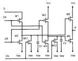
본 발명의 주사선선택구동회로는 도4와 같이 쉬프트신호를 입력받는 D단자와, set신호를 입력받는 Cu단자 및 reset신호를 입력받는 Cd단자와, 상기 Cu단자에 연결된 게이트와 상기 D단자에 연결된 소스로 이루어진 M1트랜지스터와, 상기 M1트랜지스터의 드레인에 연결된 소스와 상기 Cd단자에 연결된 게이트와 공통전압 Vss에 연결된 드레인으로 이루어진 M2트랜지스터와, 상기 Cd단자에 연결된 게이트와 외부전압 Vcc와 연결된 소스로 이루어진 M3트랜지스터와, 상기 Cu단자에 연결된 게이트와 상기 M3트랜지스터의 드레인에 연결된 소스와 공통전압 Vss에 연결된 드레인으로 이루어진 M4트랜지스터와, 상기 M1의 드레인과 상기 M2의 소스 사이의 접점 a에 연결된 게이트와 상기 외부전압 Vcc에 연결된 소스로 이루어진 M5트랜지스터와, 상기 M3트랜지스터의 소스와 상기 M4트랜지스터의 드레인 사이의 접점 b에 연결된 게이트와 상기 M5트랜지스터의 드레인에 연결된 소스와 상기 공통전압 Vss에 연결된 드레인으로 이루어진 M6트랜지스터와, 상기 a와 상기 M5트랜지스터의 게이트 사이의 접점 c에 한쪽 전극이 연결되고 다른쪽 전극은 상기 공통전압 Vss에 연결된 제1캐패시터 Ch와, 상기 b와 상기 M6트랜지스터의 게이트 사이의 접점 d에 한쪽 전극이 연결되고 다른쪽 전극은 상기 공통전압 Vss에 연결된 제2캐패시터 Cs와, 상기 M5트랜지스터의 드레인과 상기 M6트랜지스터의 소스 사이의 접점 e에서 출력단자 R이 연장된 각각의 스테이지 여러 개가 직렬로 연결되어 상기 출력단자 R이 인접하여 직렬로 연결된 다음 번째 스테이지의 D단자에 접속된 구조를 하나 이상 포함하여 구성된다.As shown in FIG. 4, the scan line selection driving circuit of the present invention includes a terminal D receiving a shift signal, a terminal Cu receiving a set signal, a terminal Cd receiving a reset signal, a gate connected to the Cu terminal, and a terminal connected to the terminal D. An M2 transistor comprising a source, a source connected to the drain of the M1 transistor, a gate connected to the Cd terminal, a drain connected to a common voltage Vss, and a source connected to the gate and the external voltage Vcc connected to the Cd terminal. An M4 transistor comprising an M3 transistor, a gate connected to the Cu terminal, a source connected to the drain of the M3 transistor, and a drain connected to a common voltage Vss, a gate connected to the contact a between the drain of the M1 and the source of the M2, and the M5 transistor consisting of a source connected to an external voltage Vcc, and the source and phase of the M3 transistor One electrode is provided at a contact c between the gate connected to the contact b between the drain of the M4 transistor, the source connected to the drain of the M5 transistor and the drain connected to the common voltage Vss, and the contact c between the a and the gate of the M5 transistor. A second capacitor Cs connected to the first capacitor Ch connected to the common voltage Vss and the contact electrode d between the b and the gate of the M6 transistor and the other electrode connected to the common voltage Vss. And at the contact e between the drain of the M5 transistor and the source of the M6 transistor, a plurality of stages each having an output terminal R extending in series are connected in series so that the output terminal R is adjacently connected in series to a D terminal of a next stage. It comprises one or more connected structures.
본 발명의 주사선선택구동회로를 보면, 상당부분이 트랜지스터로 이루어진 것을 알 수 있다. 그런데, 사실 액정패널은 TFT어레이로 이루어져 있다. 그러므로, 상기 주사선선택구동회로는 액정패널에 TFT어레이를 형성시킬 때, 같이 제조되어질 수 있는 것이다.Looking at the scan line selection driving circuit of the present invention, it can be seen that a substantial portion is composed of transistors. By the way, the liquid crystal panel actually consists of a TFT array. Therefore, the scan line selection driving circuit can be manufactured together when forming the TFT array in the liquid crystal panel.
본 발명의 주사선선택구동회로를 동작시키기 위하여 인가하는 클럭신호로는 도5와 같다. 홀수열의 주사선에 출력단자 R이 연결된 구동회로는 set신호를 CK1클럭단자에서 입력받고, reset신호를 CK2클럭단자에서 입력받으며, 짝수열의 주사선에 출력단자 R이 연결된 상기 구동회로는 set신호를 CK3클럭단자에서 입력받고, reset신호를 CK4클럭단자에서 입력받는다. 또, 첫 번째 열에 위치한 주사선에 출력신호를 인가하는 구동회로의 쉬프트단자에는 시작파형(start pulse) CKs를 인가하여 상기 주사선선택구동회로를 작동시킨다.A clock signal applied to operate the scan line selection driver circuit of the present invention is shown in FIG. The drive circuit having the output terminal R connected to the odd-numbered scanning lines receives the set signal from the CK1 clock terminal, the reset signal is inputted from the CK2 clock terminal, and the drive circuit having the output terminal R connected to the even-numbered scanning lines transmits the set signal to the CK3 clock. It receives from the terminal and reset signal from the CK4 clock terminal. In addition, a start pulse CKs is applied to a shift terminal of a drive circuit that applies an output signal to a scan line located in the first column to operate the scan line selection drive circuit.
상기 CK1, CK2, CK3 와 CK4의 주기는 도6에서와 같다. 상기 CK1가 하이(high)에서 로(low)로 떨어진 후, 다음 주기의 하이(high)가 인가되기 전에 상기 CK2에 하이(high)가 인가되었다가 로(low)로 떨어진다. 그리고, 상기 CK1이 로(low)로 떨어진 후, 상기 CK2에 하이(high)가 인가되기 전에 상기 CK3에 하이(high)가 인가되었다가 로(low)로 떨어진다. 또, 상기 CK3가 하이(high)에서 로(low)로 떨어진 후, 다음 주기의 하이(high)가 인가되기 전에 상기 CK4에 하이(high)가 인가되었다가 로(low)로 떨어진다. 상기 CK1, CK2, CK3, 및 상기 CK4는 모두 동일한 주기로 하이(high)와 로(low)가 인가된다.The cycles of CK1, CK2, CK3 and CK4 are the same as in FIG. After the CK1 falls from high to low, high is applied to the CK2 and then falls to low before the next cycle of high is applied. After the CK1 falls low, a high is applied to the CK3 before the high is applied to the CK2 and then falls to the low. In addition, after the CK3 falls from high to low, high is applied to the CK4 and then falls to low before the next cycle of high is applied. The CK1, CK2, CK3, and the CK4 are all applied with high and low at the same period.
상기 본 발명의 주사선선택구동회로의 동작을 도5와 도6을 참조로 하여 설명하면 다음과 같다. 첫 번째 스테이지에 하이(high)영역의 CKs가 쉬프트단자에 인가되는 동안, CK1이 하이(high)로 되어 M1트랜지스터와 M4트랜지스터가 동시에 도통된다. 이 때는 M2가 도통되지 않았으므로 상기 CKs의 전압이 M1트랜지스터의 소스와 드레인을 통하여 a점을 지나 M5의 게이트에 인가되면서 M5트랜지스터를 도통시킨다. 동시에 a와 M5트랜지스터의 게이트 사이의 캐패시터 CHo에 충전된다. 또, M6가 도통되지 않았으므로, 상기 도통된 M5트랜지스터를 통하여 외부전압 Vcc가 Ro단자로 인가된다.The operation of the scan line selection driving circuit according to the present invention will be described with reference to FIGS. 5 and 6 as follows. While CKs in the high region are applied to the shift terminal in the first stage, CK1 becomes high so that the M1 transistor and the M4 transistor are simultaneously conducted. At this time, since M2 is not conductive, the voltage of CKs is applied to the gate of M5 through point a through the source and drain of the M1 transistor to conduct the M5 transistor. At the same time, it is charged to the capacitor CHo between a and the gate of the M5 transistor. In addition, since M6 is not conducting, the external voltage Vcc is applied to the Ro terminal through the conducting M5 transistor.
상기 CK1이 로(low)로 떨어지면, M1트랜지스터가 단절되어 캐패시터 CH에 전압이 공급되지 않으므로 상기 CH는 방전을 하게되나, 상기 M1트랜지스터와 M2트랜지스터는 단절되어 있으므로, 상기 M5트랜지스터의 게이트로 전압을 인가한다. 그러므로, M5는 상기 CK1이 로(low)로 떨어지더라도 도통된 상태를 유지하여 Ro단자에는 지속적으로 하이(high)신호가 출력된다.When the CK1 falls to low, the M1 transistor is disconnected and no voltage is supplied to the capacitor CH. Thus, the CH discharges. However, since the M1 transistor and the M2 transistor are disconnected, the voltage is supplied to the gate of the M5 transistor. Is authorized. Therefore, M5 remains in a conductive state even when CK1 falls to low, and a high signal is continuously output to the Ro terminal.
상기 CK2가 하이(high)로 인가되기 전에 CK3가 하이(high)로 인가된다. 이 때, 첫 번째 스테이지의 출력단자 Ro에는 하이(high)신호가 유지되고 있으므로, 상기 하이(high)신호가 상기 두 번째 스테이지의 De단자에 인가된다. 즉, 상기 CK3에 의해 도통된 M1트랜지스터의 소스에 상기 Ro의 하이(high)신호가 인가되므로, 상기 두 번째 스테이지에 설치된 M5트랜지스터를 도통시킴으로써 상기 두 번째 스테이지의 Re단자에 하이(high)신호가 인가된다. 다시말해, 상기 첫 번째 스테이지의 출력단자 Ro의 하이(high)신호가 CK3가 하이(high)로 된 시간동안에는 두 번째 스테이지의 De에 인가되는 쉬프트신호로서 동작한다. 그리고, 두 번째 스테이지의 출력단자 Re의 하이(high)신호가 다음 주기의 CK1의 하이(high)시간에는 세 번째 스테이지의 Do에 인가되는 쉬프트신호로서 동작한다.CK3 is applied high before the CK2 is applied high. At this time, since a high signal is maintained at the output terminal Ro of the first stage, the high signal is applied to the De terminal of the second stage. That is, since the high signal of Ro is applied to the source of the M1 transistor conducted by CK3, the high signal is applied to the Re terminal of the second stage by conducting the M5 transistor installed in the second stage. Is approved. In other words, the high signal of the output terminal Ro of the first stage operates as a shift signal applied to the De of the second stage during the time when CK3 becomes high. The high signal of the output terminal Re of the second stage operates as a shift signal applied to the Do of the third stage at the high time of CK1 in the next period.
상기 CK3가 로(low)로 떨어지면, 상기 첫 번째 스테이지와 같이 캐패시터 CH에 충전되었던 쉬프트신호가 M5의 게이트를 도통시키므로, 두 번째 스테이지의 출력단자Re에는 지속적으로 하이(high)가 인가된다.When the CK3 falls low, the shift signal, which has been charged to the capacitor CH as in the first stage, conducts the gate of M5, so that high is continuously applied to the output terminal Re of the second stage.
상기 CK3가 로(low)로 떨어진 후, 상기 CK2가 하이(high)로 인가된다. 이 때, 상기 첫 번째 스테이지의 M2트랜지스터와 상기 M3트랜지스터가 도통된다. 그래서, 상기 캐패시터 CH에서 방전되던 전압이 M2트랜지스터로 흘러 상기 M5트랜지스터의 게이트에 전압이 인가되지 않아 상기 M5트랜지스터는 단절된다. 동시에 M3트랜지스터를 통해 외부전압이 M6트랜지스터와 캐패시터 CS에 인가되므로, M6트랜지스터는 도통되어 상기 출력단자 Ro에 공통전압 Vss가 인가되므로 Ro은 로(low)신호를 출력한다.After the CK3 falls to low, the CK2 is applied high. At this time, the M2 transistor and the M3 transistor of the first stage are conducted. Thus, the voltage discharged from the capacitor CH flows to the M2 transistor so that no voltage is applied to the gate of the M5 transistor, so that the M5 transistor is disconnected. At the same time, since an external voltage is applied to the M6 transistor and the capacitor CS through the M3 transistor, the M6 transistor is turned on so that the common voltage Vss is applied to the output terminal Ro, so Ro outputs a low signal.
상기 CK2가 로(low)로 떨어지게 되더라도 M2트랜지스터와 M3트랜지스터가 모두 단절되므로, 상기 CS에 충전되었던 전압이 M6트랜지스터의 게이트에 인가되므로, M6는 도통된 상태를 유지한다. 즉, 출력단자 Ro에는 지속적으로 로(low)신호가 출력된다.Even when the CK2 falls to low, since both the M2 and M3 transistors are disconnected, the voltage charged in the CS is applied to the gate of the M6 transistor, so that M6 remains conductive. That is, a low signal is continuously output to the output terminal Ro.
CK4에 하이(high)가 인가되기 전에 CK1에 다음 주기의 하이(high)가 인가된다. 이 때, 두 번째 스테이지의 출력단자 Re에는 하이(high)신호가 유지되고 있으므로, 상기 Re의 하이(high)신호가 세 번째 스테이지의 Do단자에 인가된다. 그래서, 상기 CK1의 하이(high)신호에 의해 도통된 상기 세 번째 스테이지의 M1트랜지스터를 통과한 상기 Do단자의 하이(high)신호가 상기 세 번째 스테이지의 M5트랜지스터를 도통시킴으로써 상기 세 번째 스테이지의 Ro단자에 하이(high)신호가 인가된다. 즉, 상기 두 번째 스테이지의 출력단자 R의 하이(high)신호가 CK1이 하이(high)로 된 시간동안에는 세 번째 스테이지의 쉬프트신호로서 동작한다는 것이다. 마찬가지로 세 번째 스테이지의 출력단자 Ro의 하이(high)신호는 CK3의 다음 주기의 하이(high)시간에는 네 번째 스테이지의 쉬프트신호로서 동작한다. 상기 CK1의 두 번째 하이(high)주기부터는 첫 번째 스테이지와 세 번째 스테이지가 동일하게 작동하고, CK1과 CK2의 하이(high)가 진행될수록 홀수스테이지가 작동한다.The next period of high is applied to CK1 before high is applied to CK4. At this time, since a high signal is maintained at the output terminal Re of the second stage, the high signal of Re is applied to the Do terminal of the third stage. Thus, the high signal of the Do terminal passing through the M1 transistor of the third stage conducted by the high signal of CK1 conducts the M5 transistor of the third stage so that Ro of the third stage is conducted. A high signal is applied to the terminal. That is, the high signal of the output terminal R of the second stage operates as the shift signal of the third stage during the time when CK1 becomes high. Similarly, the high signal of the output terminal Ro of the third stage operates as the shift signal of the fourth stage at the high time of the next period of CK3. From the second high period of the CK1, the first stage and the third stage operate the same, and the odd stage operates as the high of the CK1 and CK2 proceeds.
상기 CK1에 두 번째로 하이(high)에서 로(low)로 떨어지는 신호가 인가되면, CK4에 하이(high)가 인가된다. 이 때, 상기 두 번째 스테이지의 M2트랜지스터와 M3트랜지스터가 도통된다. 그래서, 상기 캐패시터 CH에서 방전되던 전압이 M2트랜지스터로 흘러 상기 M5트랜지스터의 게이트에 전압이 인가되지 않아 상기 M5트랜지스터는 단절된다. 동시에 M3트랜지스터를 통해 외부전압이 M6트랜지스터와 캐패시터 Cs에 인가되므로, M6트랜지스터는 도통되어 상기 출력단자 Re에 공통전압 Vss가 인가되므로, Re는 로(low)신호를 출력한다.When a signal falling from high to low for the second time is applied to CK1, high is applied to CK4. At this time, the M2 transistor and the M3 transistor of the second stage become conductive. Thus, the voltage discharged from the capacitor CH flows to the M2 transistor so that no voltage is applied to the gate of the M5 transistor, so that the M5 transistor is disconnected. At the same time, since an external voltage is applied to the M6 transistor and the capacitor Cs through the M3 transistor, the M6 transistor is turned on so that the common voltage Vss is applied to the output terminal Re, so Re outputs a low signal.
상기 CK4가 로(low)로 떨어지게 되더라도 M2 트랜지스터와 M3트랜지스터가 모두 단절되어 상기 Cs에 충전되었던 전압이 M6트랜지스터의 게이트에 인가되므로, M6는 도통된 상태를 유지한다. 즉, 출력단자 Re에는 지속적으로 로(low)신호가 출력되는 것이다.Even when the CK4 falls to low, since both the M2 transistor and the M3 transistor are disconnected and the voltage charged in the Cs is applied to the gate of the M6 transistor, M6 remains in a conductive state. That is, a low signal is continuously output to the output terminal Re.
본 발명의 주사선선택구동회로는 종래의 주사선선택구동회로에 비해 적은 수의 트랜지스터로 꾸며질 수 있다. 그러므로, 액정패널의 TFT어레이를 형성하는 것과 동시에 주사선선택구동회로가 만들기가 쉽다. 즉, 종래보다 쉽게 주사선선택구동회로가 액정패널에 일체화될 수 있다는 것이다.The scan line selection driver circuit of the present invention can be decorated with fewer transistors than the conventional scan line selection driver circuit. Therefore, it is easy to form a scanning line selection driving circuit at the same time as forming the TFT array of the liquid crystal panel. That is, the scan line selection driving circuit can be integrated in the liquid crystal panel more easily than in the prior art.
(실시예2)Example 2
본 발명의 주사선선택구동회로를 도5에서 나타낸 회로에 덧붙여 도7에서 보는 것처럼 설계할 수도 있다. 즉, 상기 본 발명의 실시예1에 덧붙여 M1트랜지스터의 드레인과 M2트랜지스터의 소스 사이의 접점 a를 M5트랜지스터의 게이트와 공유하도록 상기 M5트랜지스터와 병렬로 연결된 게이트와 외부전압 Vcc에 연결된 소스로 이루어진 M7트랜지스터와, 상기 M3트랜지스터의 드레인과 M4트랜지스터의 소스 사이의 접점 b를 M6의 게이트와 공유하도록 상기 M6트랜지스터와 병렬로 연결된 게이트와 공통전압 Vss에 연결된 소스와 상기 M7트랜지스터의 드레인과 연결된 소스로 이루어진 M8트랜지스터와, 상기 M8트랜지스터의 게이트와 상기 접점 b 사이의 접점 f에 한쪽 전극이 연결되고, 상기 공통전압 Vss에 다른쪽 전극이 연결된 제3캐패시터 Cs'으로 이루어고, 상기 M7트랜지스터의 드레인과 상기 M8트랜지스터의 소스 사이의 접점 g에 쉬프트신호가 출력되는 RC단자로 구성되도록 할 수도 있다는 것이다.The scanning line selection driving circuit of the present invention may be designed as shown in FIG. 7 in addition to the circuit shown in FIG. That is, in addition to
상기 실시예2에서 제조된 주사선선택구동회로의 구성은 실시예1에서 제조된 주사선선택구동회로와 비슷하다. 그러므로, 액정패널에 TFT어레이와 일체로 형성될 수 있다. 다만, 상기 실시예2의 주사선선택구동회로는 액정패널의 주사선이 R단자에 연결되어 있고, 인접한 상기 주사선선택구동회로의 쉬프트단자 D는 상기 RC단자에 연결되어 있는 것이 다르다. 도8은 실시예2에서의 주사선선택구동회로의 전체 구성도를 나타낸 도면이다.The configuration of the scan line selection driver circuit manufactured in the second embodiment is similar to that of the scan line selection driver circuit manufactured in the first embodiment. Therefore, it can be formed integrally with the TFT array in the liquid crystal panel. However, in the scan line selection driver circuit of
또한, 상기 실시예2에서 제조된 주사선선택구동회로의 동작은 상기 실시예1에서 제조된 주사선선택구동회로의 동작과 유사하다. 다만, 상기 M5트랜지스터와 상기 M7트랜지스터가 동일한 시간에 도통(on)되고 단절(off)되며, 상기 M6트랜지스터와 상기 M8트랜지스터가 동일한 시간에 도통되고 단절된다. 그래서, 상기 R과 상기 RC의 신호파형은 사실상 동일하다.In addition, the operation of the scan line selection driver circuit manufactured in the second embodiment is similar to the operation of the scan line selection driver circuit manufactured in the first embodiment. However, the M5 transistor and the M7 transistor are turned on and disconnected at the same time, and the M6 transistor and the M8 transistor are turned on and disconnected at the same time. Thus, the signal waveforms of R and RC are substantially the same.
실시예1과 마찬가지로 본 실시예2의 주사선선택구동회로도 종래 발명에 비해 적은 수의 트랜지스터로 꾸며질 수 있다. 즉, 액정패널의 TFT어레이를 형성하는 것과 동시에 주사선선택구동회로가 만들어질 수 있다는 것이다. 다시 말해, 종래보다 쉽게 주사선선택구동회로가 액정패널에 일체화될 수 있다는 것이다.Like the first embodiment, the scan line selection driving circuit of the second embodiment can be decorated with fewer transistors than the conventional invention. That is, the scanning line selection driving circuit can be made at the same time as forming the TFT array of the liquid crystal panel. In other words, the scan line selection driving circuit can be integrated in the liquid crystal panel more easily than in the prior art.
(실시예3)Example 3
상기 실시예1과 실시예2에서의 회로는 액정패널에 동시에 형성되므로, 회로의 일부분에 불량이 발생하면, 액정패널 전체를 사용하지 못하게 되는 불상사가 발생할 수도 있다. 그래서, 본 실시예3은 출력단자와 주사선 사이에 형성된 스위치소자의 한쪽 전극이 스위치단자에 공통적으로 연결된 주사선선택구동회로를 액정패널에 복수개 설치하여 이상이 발생한 주사선선택구동회로의 스위치소자를 단절(off)시켜 작동불능시키고, 정상작동하는 주사선선택구동회로의 스위치소자를 도통(on)시킴으로써 액정패널을 작동시킬수 있도록 한다.Since the circuits of the first embodiment and the second embodiment are formed in the liquid crystal panel at the same time, if a defect occurs in a part of the circuit, an undesired accident may occur that the entire liquid crystal panel cannot be used. Thus, in the third embodiment, a plurality of scan line selection driver circuits in which one electrode of the switch element formed between the output terminal and the scan line is commonly connected to the switch terminals are provided in the liquid crystal panel to disconnect the switch elements of the scan line selection driver circuit in which the abnormality occurs ( the liquid crystal panel is operated by turning off the switch element of the scan line selection driving circuit which is normally operated.
도9를 참조로 본 발명의 실시예3을 설명하겠다. 실시예1과 실시예2에서와 마찬가지로 액정패널의 박막트랜지스터를 형성할 때, 주사선선택구동회로의 박막트랜지스터를 동시에 형성한다. 다만, 본 실시예3에서는 TFT어레이의 양쪽에 하나씩 두 개의 주사선선택구동회로를 형성한다. 이 개수는 필요에 따라 더 형성시킬 수도 있다. 또, 상기 주사선선택구동회로의 각 출력단자 R에 스위치소자로서의 박막트랜지스터(120)를 형성하고, 상기 스위치소자로서 사용되는 박막트랜지스터의 게이트에 공통적으로 접속된 스위치단자 ENR, ENL를 만든다.A third embodiment of the present invention will be described with reference to FIG. As in the first and second embodiments, when the thin film transistor of the liquid crystal panel is formed, the thin film transistor of the scan line selection driver circuit is formed at the same time. However, in the third embodiment, two scanning line selection driving circuits are formed, one on each side of the TFT array. This number may be further formed as necessary. Further, a
이 때, 상기 주사선선택구동회로는 액정패널의 주사선에 출력신호를 인가할 수 있는 회로로 구성되되, 상기 주사선의 양 끝단에 각각 형성된다. 즉, 동일한 주사선에 두 개의 구동부가 연결되도록 한다는 것이다. 그래서, 제조공정 중에 상기 두 개의 구동부 중, 어느 하나의 구동부에 불량이 발생하면, 상기 불량이 발생한 구동부의 스위치단자에 로(low)신호를 인가하여 불량구동부의 출력단자에 연결된 스위치소자를 단절(off)시키고, 정상적인 동작을 하는 구동부의 스위치단자에 하이(high)신호를 인가하여 정상구동부의 출력단자에 연결된 스위치소자를 도통(on)시킨다.In this case, the scan line selection driver circuit is composed of a circuit capable of applying an output signal to the scan line of the liquid crystal panel, and is formed at both ends of the scan line. That is, two driving units are connected to the same scan line. Thus, when a failure occurs in any one of the two driving units during the manufacturing process, a low signal is applied to the switch terminal of the driving unit where the failure occurs to disconnect the switch element connected to the output terminal of the defective driving unit ( off), and a high signal is applied to the switch terminal of the driving unit for normal operation to turn on the switch element connected to the output terminal of the normal driving unit.
확률적으로 살펴볼 때, 하나의 구동부에 불량이 발생하는 것보다 두 개의 구동부에서 동시에 불량이 발생하는 확률은 매우 낮으므로, 상술한 본 발명의 액정표시장치는 액정패널의 제조공정에서 구동부에 이상이 발생하더라도 사용에는 아무런 문제가 없다. 따라서, 전체적인 수율을 떨어뜨리지 않고 주사선선택구동회로와 패널이 일체화된 액정표시장치의 제조가 가능해진다.In view of the probability, since the probability of a failure occurring in two driving units at the same time is much lower than that of a failure in one driving unit, the above-described liquid crystal display of the present invention has an abnormality in the driving unit in the manufacturing process of the liquid crystal panel. Even if it occurs, there is no problem in use. Accordingly, it is possible to manufacture the liquid crystal display device in which the scan line selection driving circuit and the panel are integrated without degrading the overall yield.
본 발명에서 상기 구동부는 출력단자가 주사선에 연결된다면, 종래의 어떤 회로에도 적용시킬 수가 있다. 그리고, 제조공정 중에 상기 각각의 구동부를 테스트하여 이상이 발생한 구동부를 패널의 완성단계에서 레이저(Laser) 등을 이용하여 제거해도 된다.In the present invention, if the output terminal is connected to the scan line, the driving unit can be applied to any conventional circuit. In addition, you may test each said drive part during a manufacturing process, and may remove the drive part which generate | occur | produced using a laser etc. at the completion stage of a panel.
(실시예4)Example 4
실시예3에서는 출력단자에 직접 스위치소자를 연결하였으나, 구동부의 내부에 스위치소자를 내장시킬 수도 있다. 도10을 참조로 본 발명의 실시예4를 설명하겠다.In Embodiment 3, the switch element is directly connected to the output terminal, but the switch element may be incorporated in the driving unit. A fourth embodiment of the present invention will be described with reference to FIG.
본 실시예4는 소정의 주기로 set신호를 인가받는 CK단자 및 reset 신호를 인가받는 CR단자와, 상기 CK단자와 CR단자에 인가되는 신호에 따라 액정패널의 주사선에 구동신호를 인가하는 출력단자 R과, 쉬프트신호를 인가받는 쉬프트입력단자 D가 있고, 상기 출력단자 R에 스위칭하는 수단 ME1 및 ME2를 포함하여 하나의 스테이지로 구성된 구동회로가 하나 이상 직렬로 연결되어 형성된 구조가 하나의 구동부를 이루고 있다. 그리고, 상기 ME1과 ME2는 스위칭신호를 입력받는 스위치단자 EN에 연결되어 있다. 상기 스위칭하는 수단으로 박막트랜지스터를 사용하면, 액정패널과 일체화시키기 쉽다.In the fourth embodiment, the CK terminal receiving the set signal and the CR terminal receiving the reset signal at predetermined cycles, and the output terminal R applying the driving signal to the scan line of the liquid crystal panel according to the signals applied to the CK terminal and the CR terminal And a shift input terminal D to which a shift signal is applied, and a structure in which one or more driving circuits including one stage ME1 and ME2 are connected in series including the means ME1 and ME2 for switching to the output terminal R constitutes one driving unit. have. The ME1 and the ME2 are connected to a switch terminal EN for receiving a switching signal. When a thin film transistor is used as the means for switching, it is easy to integrate with the liquid crystal panel.
본 발명이 실시예3과 다른 점은 실시예3에서는 출력되는 구동신호를 주사선에 전달하는 것을 제어하는 데 반해, 상기 실시예2에서는 ME1과 ME2가 구동신호의 발생을 제어한다는 것이다. 즉, ME1과 ME2의 스위치단자 EN에 하이(high)신호를 인가함으로써 상기 구동부에서 구동신호가 발생하지 않도록 할 수 있다는 것이다.The present invention differs from the third embodiment in that the third embodiment controls the transfer of the output drive signal to the scanning line, whereas in the second embodiment, ME1 and ME2 control the generation of the drive signal. That is, by applying a high signal to the switch terminals EN of the ME1 and the ME2, the driving signal can be prevented from being generated in the driver.
실시예3는 박막트랜지스터(120)에 의한 구동신호의 감쇄가 발생하므로, 구동부의 구동능력을 크게 해 주어야 한다.In Embodiment 3, since the attenuation of the driving signal by the
그래서, 구동부와 액정패널을 일체화시켜 제조하는 공정에서 상기 구동부의 일부분에 불량이 발생하면, 상기 불량이 발생한 구동부의 스위치단자(EN)에 하이(high)신호를 인가하여 스위치소자(ME1, ME2)를 도통(on)시킴으로써 상기 출력단자에 오픈상태(high임피던스 상태)로 만들 수 있다. 따라서 실시예3에서 발생하는 구동부의 구동능력을 크게 해 주어야 하는 문제점을 극복할 수 있다.Thus, when a defect occurs in a part of the driver in the process of manufacturing the driver and the liquid crystal panel integrally, a high signal is applied to the switch terminal EN of the driver in which the defect occurs and the switch elements ME1 and ME2 are applied. By turning on, the output terminal can be made open (high impedance state). Therefore, it is possible to overcome the problem of increasing the driving capability of the driving unit generated in the third embodiment.
본 실시예4에서도 상기 실시예3과 마찬가지로 제조공정 중에 상기 각각의 주사선선택구동회로를 테스트하여 이상이 발생한 주사선선택구동회로의 부분을 패널의 완성단계에서 레이저(Laser) 등을 이용하여 제거해도 된다.In the fourth embodiment, similarly to the third embodiment, the scan line selection driver circuits may be tested during the manufacturing process to remove portions of the scan line selection driver circuits in which abnormalities are generated by using a laser or the like at the completion of the panel. .
본 발명의 주사선선택구동회로는 종래에 비해 단위 스테이지 당 사용된 트랜지스터의 개수가 적어 구조가 간단하다. 뿐만아니라 주사선에 인가할 출력신호를 형성하기 위하여 외부로부터 인가받는 외부클럭신호와 외부전압을 위한 리드선의 개수가 적어 액정패널과의 연결이 단순해져 상기 본 발명의 주사선선택구동회로를 사용하면, 액정표시장치를 종래보다 간단히 제조할 수 있다. 그러므로, 제조수율이 높아지고 제조단가가 낮아지게 된다.The scan line selection driving circuit of the present invention has a simpler structure since the number of transistors used per unit stage is smaller than in the related art. In addition, since the number of external clock signals applied from the outside and the number of lead wires for external voltages are small to form an output signal to be applied to the scan lines, the connection with the liquid crystal panel is simplified, and thus the liquid crystal display apparatus of the present invention can be used. The display device can be manufactured simpler than before. Therefore, the production yield is increased and the manufacturing cost is lowered.
또한, 각 클럭단자에 인가되는 하이(high)신호의 시간차를 고려할 필요가 없어 종래보다 쉽게 제어할 수 있다는 장점도 있다. 상기 본 발명의 주사선선택구동회로를 제어하는 데 있어서, 클럭신호 CK1, CK2, CK3 및 CK4의 주기를 조절함으로써 액정패널의 주사선에 인가하는 출력신호 R의 하이(high)시간이 조절된다.In addition, it is not necessary to consider the time difference of the high signal applied to each clock terminal, there is an advantage that it can be controlled more easily than the conventional. In controlling the scan line selection driver circuit of the present invention, the high time of the output signal R applied to the scan line of the liquid crystal panel is adjusted by adjusting the period of the clock signals CK1, CK2, CK3 and CK4.
그리고, 상기 본 발명의 주사선선택구동회로에서 사용되는 TFT의 재료로는 a-Si 및 poly-Si 둘다 사용될 수 있어 액정패널의 TFT어레이를 제조하는 공정에서 동시에 제조될 수 있으므로, 패키지화하는 비용이 절감된다. 게다가 액정패널 위에 주사선선택구동회로를 동시에 실장시킬 수 있으므로, 구조가 상당히 간단해진다.In addition, both a-Si and poly-Si may be used as the material of the TFT used in the scan line selection driving circuit of the present invention, and thus, the cost of packaging may be reduced because the TFT may be manufactured simultaneously in the process of manufacturing the TFT array of the liquid crystal panel. do. In addition, since the scanning line selection driving circuit can be mounted on the liquid crystal panel at the same time, the structure is considerably simpler.
그리고, 확률적으로 미루어 볼 때, 하나의 주사선선택구동회로보다는 두 개의 주사선선택구동회로에서 모두 불량이 발생하는 확률이 더 적다. 그런데, 액정패널은 내장된 주사선선택구동회로가 하나만 양호해도 정상적으로 작동된다. 그러므로, 본 발명에서 실시예3과 실시예4에 나타낸 액정패널은 어떤 주사선선택구동회로를 일체화시키더라도 패널 전체의 제조수율을 향상시킬 수 있다.In addition, stochastically, the probability that a defect occurs in both scan line selection driver circuits is less than that of one scan line selection driver circuit. However, the liquid crystal panel operates normally even if only one scan line selection driving circuit is incorporated. Therefore, in the present invention, the liquid crystal panels shown in the third and fourth embodiments can improve the manufacturing yield of the entire panel even when any scan line selection driving circuit is integrated.
Claims (7)
Translated fromKoreanPriority Applications (2)
| Application Number | Priority Date | Filing Date | Title |
|---|---|---|---|
| KR1019970000293AKR100235589B1 (en) | 1997-01-08 | 1997-01-08 | Driving Method of Thin Film Transistor Liquid Crystal Display |
| US08/996,815US6067067A (en) | 1997-01-08 | 1997-12-23 | Scan driver IC for a liquid crystal display |
Applications Claiming Priority (1)
| Application Number | Priority Date | Filing Date | Title |
|---|---|---|---|
| KR1019970000293AKR100235589B1 (en) | 1997-01-08 | 1997-01-08 | Driving Method of Thin Film Transistor Liquid Crystal Display |
Publications (2)
| Publication Number | Publication Date |
|---|---|
| KR19980065362A KR19980065362A (en) | 1998-10-15 |
| KR100235589B1true KR100235589B1 (en) | 1999-12-15 |
Family
ID=19494281
Family Applications (1)
| Application Number | Title | Priority Date | Filing Date |
|---|---|---|---|
| KR1019970000293AExpired - LifetimeKR100235589B1 (en) | 1997-01-08 | 1997-01-08 | Driving Method of Thin Film Transistor Liquid Crystal Display |
Country Status (2)
| Country | Link |
|---|---|
| US (1) | US6067067A (en) |
| KR (1) | KR100235589B1 (en) |
Families Citing this family (10)
| Publication number | Priority date | Publication date | Assignee | Title |
|---|---|---|---|---|
| JP3680601B2 (en)* | 1998-05-14 | 2005-08-10 | カシオ計算機株式会社 | SHIFT REGISTER, DISPLAY DEVICE, IMAGING ELEMENT DRIVE DEVICE, AND IMAGING DEVICE |
| KR100438525B1 (en) | 1999-02-09 | 2004-07-03 | 엘지.필립스 엘시디 주식회사 | Shift Register Circuit |
| DE19950860B4 (en)* | 1998-10-21 | 2009-08-27 | Lg Display Co., Ltd. | shift register |
| KR100365499B1 (en)* | 2000-12-20 | 2002-12-18 | 엘지.필립스 엘시디 주식회사 | Method and Apparatus of Liquid Crystal Display |
| JP4761643B2 (en)* | 2001-04-13 | 2011-08-31 | 東芝モバイルディスプレイ株式会社 | Shift register, drive circuit, electrode substrate, and flat display device |
| JP4789369B2 (en)* | 2001-08-08 | 2011-10-12 | 株式会社半導体エネルギー研究所 | Display device and electronic device |
| KR100815897B1 (en)* | 2001-10-13 | 2008-03-21 | 엘지.필립스 엘시디 주식회사 | Data driving device and method of liquid crystal display |
| KR101152129B1 (en)* | 2005-06-23 | 2012-06-15 | 삼성전자주식회사 | Shift register for display device and display device including shift register |
| CN105096876B (en)* | 2015-08-19 | 2017-06-27 | 深圳市华星光电技术有限公司 | GOA drive systems and liquid crystal panel |
| CN105632383B (en)* | 2016-01-11 | 2018-09-11 | 京东方科技集团股份有限公司 | A kind of test circuit, test method, display panel and display device |
Family Cites Families (8)
| Publication number | Priority date | Publication date | Assignee | Title |
|---|---|---|---|---|
| DE69232910T2 (en)* | 1991-02-28 | 2003-11-13 | Thales Avionics Lcd S.A., Puteaux | Redundant shift registers for scanning devices |
| DE69332935T2 (en)* | 1992-12-10 | 2004-02-26 | Sharp K.K. | Flat display device, its control method and method for its production |
| US5313222A (en)* | 1992-12-24 | 1994-05-17 | Yuen Foong Yu H. K. Co., Ltd. | Select driver circuit for an LCD display |
| US5619223A (en)* | 1994-04-14 | 1997-04-08 | Prime View Hk Limited | Apparatus for increasing the effective yield of displays with integregated row select driver circuit |
| US5510805A (en)* | 1994-08-08 | 1996-04-23 | Prime View International Co. | Scanning circuit |
| US5648790A (en)* | 1994-11-29 | 1997-07-15 | Prime View International Co. | Display scanning circuit |
| US5701136A (en)* | 1995-03-06 | 1997-12-23 | Thomson Consumer Electronics S.A. | Liquid crystal display driver with threshold voltage drift compensation |
| US5710571A (en)* | 1995-11-13 | 1998-01-20 | Industrial Technology Research Institute | Non-overlapped scanning for a liquid crystal display |
- 1997
- 1997-01-08KRKR1019970000293Apatent/KR100235589B1/ennot_activeExpired - Lifetime
- 1997-12-23USUS08/996,815patent/US6067067A/ennot_activeExpired - Lifetime
Also Published As
| Publication number | Publication date |
|---|---|
| US6067067A (en) | 2000-05-23 |
| KR19980065362A (en) | 1998-10-15 |
Similar Documents
| Publication | Publication Date | Title |
|---|---|---|
| KR100235590B1 (en) | Driving Method of Thin Film Transistor Liquid Crystal Display | |
| US5506516A (en) | Method of inspecting an active matrix substrate | |
| US6337677B1 (en) | Liquid crystal display device, driving method for liquid crystal display devices, and inspection method for liquid crystal display devices | |
| KR100449437B1 (en) | Image display device | |
| US11662865B2 (en) | Array substrate and driving method, display panel and touch display device | |
| US20070040572A1 (en) | Electrical inspection method and method of fabricating semiconductor display devices | |
| JP2010186537A (en) | Shift register driving method, shift register, and liquid crystal display device provided with the same | |
| US6897841B2 (en) | Liquid crystal display device and electronic apparatus comprising it | |
| US5745090A (en) | Wiring structure and driving method for storage capacitors in a thin film transistor liquid crystal display device | |
| CN111223449B (en) | A display panel, its driving method and display device | |
| KR100384214B1 (en) | Flat display device, display control device and display control method | |
| KR100533610B1 (en) | Driving circuit and display device using same | |
| KR100628937B1 (en) | Active Matrix Liquid Crystal Display Device | |
| KR100235589B1 (en) | Driving Method of Thin Film Transistor Liquid Crystal Display | |
| JPH05210089A (en) | Active matrix display device and driving method thereof | |
| US6292163B1 (en) | Scanning line driving circuit of a liquid crystal display | |
| CN110426900A (en) | Array substrate, display panel and display device | |
| US20020000965A1 (en) | Circuit panel and flat-panel display device | |
| JP3345349B2 (en) | Shift register circuit and image display device | |
| JP3146959B2 (en) | Liquid crystal display device and shift register circuit thereof | |
| JPH10161157A (en) | Semiconductor device for display | |
| US6590551B1 (en) | Apparatus and method for driving scanning lines of liquid crystal panel with flicker reduction function | |
| JPH02296286A (en) | Substrate for liquid crystal display and driving method thereof | |
| JP3240837B2 (en) | Display semiconductor device | |
| JPH05307167A (en) | Active matrix panel |
Legal Events
| Date | Code | Title | Description |
|---|---|---|---|
| A201 | Request for examination | ||
| PA0109 | Patent application | Patent event code:PA01091R01D Comment text:Patent Application Patent event date:19970108 | |
| PA0201 | Request for examination | Patent event code:PA02012R01D Patent event date:19970108 Comment text:Request for Examination of Application | |
| PG1501 | Laying open of application | ||
| E902 | Notification of reason for refusal | ||
| PE0902 | Notice of grounds for rejection | Comment text:Notification of reason for refusal Patent event date:19990322 Patent event code:PE09021S01D | |
| E701 | Decision to grant or registration of patent right | ||
| PE0701 | Decision of registration | Patent event code:PE07011S01D Comment text:Decision to Grant Registration Patent event date:19990626 | |
| N231 | Notification of change of applicant | ||
| PN2301 | Change of applicant | Patent event date:19990903 Comment text:Notification of Change of Applicant Patent event code:PN23011R01D | |
| GRNT | Written decision to grant | ||
| PR0701 | Registration of establishment | Comment text:Registration of Establishment Patent event date:19990927 Patent event code:PR07011E01D | |
| PR1002 | Payment of registration fee | Payment date:19990928 End annual number:3 Start annual number:1 | |
| PG1601 | Publication of registration | ||
| PR1001 | Payment of annual fee | Payment date:20020624 Start annual number:4 End annual number:4 | |
| PR1001 | Payment of annual fee | Payment date:20030701 Start annual number:5 End annual number:5 | |
| PR1001 | Payment of annual fee | Payment date:20040629 Start annual number:6 End annual number:6 | |
| PR1001 | Payment of annual fee | Payment date:20050627 Start annual number:7 End annual number:7 | |
| PR1001 | Payment of annual fee | Payment date:20060629 Start annual number:8 End annual number:8 | |
| PR1001 | Payment of annual fee | Payment date:20070702 Start annual number:9 End annual number:9 | |
| PR1001 | Payment of annual fee | Payment date:20080701 Start annual number:10 End annual number:10 | |
| PR1001 | Payment of annual fee | Payment date:20090622 Start annual number:11 End annual number:11 | |
| PR1001 | Payment of annual fee | Payment date:20100621 Start annual number:12 End annual number:12 | |
| PR1001 | Payment of annual fee | Payment date:20110615 Start annual number:13 End annual number:13 | |
| PR1001 | Payment of annual fee | Payment date:20120628 Start annual number:14 End annual number:14 | |
| FPAY | Annual fee payment | Payment date:20130619 Year of fee payment:15 | |
| PR1001 | Payment of annual fee | Payment date:20130619 Start annual number:15 End annual number:15 | |
| FPAY | Annual fee payment | Payment date:20140630 Year of fee payment:16 | |
| PR1001 | Payment of annual fee | Payment date:20140630 Start annual number:16 End annual number:16 | |
| FPAY | Annual fee payment | Payment date:20150818 Year of fee payment:17 | |
| PR1001 | Payment of annual fee | Payment date:20150818 Start annual number:17 End annual number:17 | |
| FPAY | Annual fee payment | Payment date:20160816 Year of fee payment:18 | |
| PR1001 | Payment of annual fee | Payment date:20160816 Start annual number:18 End annual number:18 | |
| EXPY | Expiration of term | ||
| PC1801 | Expiration of term |