KR100235212B1 - A field emission cathode and maunfacture thereof - Google Patents
A field emission cathode and maunfacture thereofDownload PDFInfo
- Publication number
- KR100235212B1 KR100235212B1KR1019970003686AKR19970003686AKR100235212B1KR 100235212 B1KR100235212 B1KR 100235212B1KR 1019970003686 AKR1019970003686 AKR 1019970003686AKR 19970003686 AKR19970003686 AKR 19970003686AKR 100235212 B1KR100235212 B1KR 100235212B1
- Authority
- KR
- South Korea
- Prior art keywords
- layer
- cathode
- resistance
- resistive
- field emission
- Prior art date
- Legal status (The legal status is an assumption and is not a legal conclusion. Google has not performed a legal analysis and makes no representation as to the accuracy of the status listed.)
- Expired - Fee Related
Links
Images


Classifications
- H—ELECTRICITY
- H01—ELECTRIC ELEMENTS
- H01J—ELECTRIC DISCHARGE TUBES OR DISCHARGE LAMPS
- H01J9/00—Apparatus or processes specially adapted for the manufacture, installation, removal, maintenance of electric discharge tubes, discharge lamps, or parts thereof; Recovery of material from discharge tubes or lamps
- H01J9/02—Manufacture of electrodes or electrode systems
- H—ELECTRICITY
- H01—ELECTRIC ELEMENTS
- H01J—ELECTRIC DISCHARGE TUBES OR DISCHARGE LAMPS
- H01J1/00—Details of electrodes, of magnetic control means, of screens, or of the mounting or spacing thereof, common to two or more basic types of discharge tubes or lamps
- H01J1/02—Main electrodes
- H01J1/30—Cold cathodes, e.g. field-emissive cathode
- H01J1/304—Field-emissive cathodes
- H01J1/3042—Field-emissive cathodes microengineered, e.g. Spindt-type
- H—ELECTRICITY
- H01—ELECTRIC ELEMENTS
- H01J—ELECTRIC DISCHARGE TUBES OR DISCHARGE LAMPS
- H01J1/00—Details of electrodes, of magnetic control means, of screens, or of the mounting or spacing thereof, common to two or more basic types of discharge tubes or lamps
- H01J1/02—Main electrodes
- H01J1/30—Cold cathodes, e.g. field-emissive cathode
- H—ELECTRICITY
- H01—ELECTRIC ELEMENTS
- H01J—ELECTRIC DISCHARGE TUBES OR DISCHARGE LAMPS
- H01J9/00—Apparatus or processes specially adapted for the manufacture, installation, removal, maintenance of electric discharge tubes, discharge lamps, or parts thereof; Recovery of material from discharge tubes or lamps
- H01J9/02—Manufacture of electrodes or electrode systems
- H01J9/022—Manufacture of electrodes or electrode systems of cold cathodes
- H01J9/025—Manufacture of electrodes or electrode systems of cold cathodes of field emission cathodes
- H—ELECTRICITY
- H01—ELECTRIC ELEMENTS
- H01J—ELECTRIC DISCHARGE TUBES OR DISCHARGE LAMPS
- H01J2201/00—Electrodes common to discharge tubes
- H01J2201/30—Cold cathodes
- H01J2201/319—Circuit elements associated with the emitters by direct integration
Landscapes
- Engineering & Computer Science (AREA)
- Manufacturing & Machinery (AREA)
- Cold Cathode And The Manufacture (AREA)
- Cathode-Ray Tubes And Fluorescent Screens For Display (AREA)
Abstract
Translated fromKoreanDescription
Translated fromKorean(발명이 속하는 기술분야)(Technical field to which the invention belongs)
본 발명은 콜드캐소드(cold cathode)로서 알려져 있는 전계방출 캐소드 및 그 제조방법에 관한 것이다.Field of the Invention The present invention relates to field emission cathodes known as cold cathodes and methods for their preparation.
(종래의 기술)(Conventional technology)
금속 또는 반도체표면의 인가전압을 109[V/m] 정도로 하면, 터널효과에 의하여 전자가 전위장벽을 통과하여, 상온에서도 진공중에 전자방출이 행해진다. 이를 전계방출(Field Emission)이라 부르고, 이와같은 원리로 전자를 방출하는 캐소드를 전계방출 캐소드(Field Emission Cathode; 이하 FEC로 나타냄), 또는 전계방출소자라 부르고 있다.When the applied voltage of the metal or semiconductor surface is about 109 [V / m], electrons pass through the potential barrier due to the tunnel effect, and electrons are emitted in vacuum even at room temperature. This is called field emission, and the cathode that emits electrons in this manner is called a field emission cathode (hereinafter referred to as FEC), or a field emission device.
근래에, 반도체 미세가공 기술을 이용하여, 마이크론 크기의 전계방출 캐소드로 이루어지는 표면 방출형의 전계방출 캐소드의 제작이 가능하게 되었고, 복수의 전계방출 캐소드를 기판상에 형성한 것은 그 각 이미터로부터 방출된 전자를 형광면에 조사함으로써 평면형의 표시장치나 각종 전자장치를 구성하는 전자 공급수단으로서 기대되고 있다.In recent years, it has become possible to manufacture surface-emitting field emission cathodes consisting of micron-sized field emission cathodes using semiconductor micromachining techniques, and it is possible to form a plurality of field emission cathodes on a substrate from each emitter. The emitted electrons are irradiated onto the fluorescent surface to be expected as electron supply means constituting flat display devices and various electronic devices.
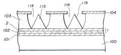
이와같은 전계방출 캐소드의 일예로서 스핀트(spindt)형이라 불리우는 전계방출 캐소드의 사시도를 도 4에 도시하다.4 shows a perspective view of a field emission cathode, called a spindt type, as an example of such a field emission cathode.
이 도면에서, 기판(100)상에 캐소드 전극층(101)이 형성되어 있고, 그 캐소드전극층(101)상에 저항층(102), 절연층(103) 및 게이트 전극층(104)의 막이 차례로 형성되어 있다. 그리고 절연층(103)에 형성된 홀내에 이미터콘(115)이 형성되어 있고, 그 이미터콘(115)의 선단부분은 게이트전극층(104)의 개구부에 위치하고 있다.In this figure, the
이러한 FEC에 있어서는 미세가공 기술을 사용함으로써 이미터콘(115)과 게이트 전극층(104)과의 거리를 서브마이크론 단위로 할 수 있기 때문에, 이미터콘(115)와 게이트 전극층(104) 사이에 단지 수십볼트의 전압을 인가함으로써도, 이미터콘(115)으로부터 전자를 방출시킬 수 있다.In this FEC, the distance between the
따라서, 도 4에 도시하는 바와 같이 상기의 FEC가 어레이형상으로 복수개가 형성되어 있는 기판(100)의 상방에 형광재료가 도포되어 있는 애노드기판(116)을 배치하고 전압(VGE, VA)을 인가하면, 방출된 전자에 의하여 형광재를 발광시킬 수 있는 표시장치로 될 수 있다.Therefore, as shown in FIG. 4, the
여기서, 이미터콘(115)과 캐소드전극층(101) 사이에 저항층(102)이 설치되어 있는 이유는 다음과 같다. 즉, 이미터콘과 게이트 전극과의 거리가 매우 짧게 되어 있기 때문에 제조과정에 있어서, 먼지 등에 의하여 이미터콘과 게이트 전극이 단락하는 경우가 있다. 게이트 전극과 이미터콘이 하나라도 단락하면, 모든 게이트 전극과 이미터콘 사이에 전압이 인가되지 못하게 되고 동작 불능으로 된다.Here, the reason why the
또한, FEC 초기의 동작시에 국부적인 이탈가스가 생기고, 그 가스에 의하여 이미터콘과 게이트 전극 또는 애노드 전극 사이에 방전이 일어나는 경우가 있고, 이 때문에 대전류가 캐소드에 흘러 캐소드가 파괴되는 경우가 있었다.In addition, a local release gas is generated during the initial operation of the FEC, and discharge may occur between the emitter cone and the gate electrode or the anode electrode by the gas, which causes a large current to flow to the cathode, thereby destroying the cathode. .
더욱이, 복수의 이미터콘 중의 전자가 방출하기 쉬운 이미터콘에 전자의 방출이 집중되기 때문에, 그 이미터콘에 전류가 집중하여, 화면상에 이상하게 밝은 스팟(spot)이 발생하는 경우가 있었다.Furthermore, since electrons are concentrated in the emitter cones in which the electrons in the plurality of emitter cones are easy to emit, the current is concentrated in the emitter cones, so that unusually bright spots may occur on the screen.
여기서, 이미터콘(115)과 캐소드 전극층(101) 사이에 저항층(102)을 설치함으로써, 어떤 이미터콘(115)으로 부터의 방출전자가 많아지면, 그 이미터콘(115)에 흐르는 전류의 증가에 따라 상기 저항층(102)에 의하여 그 이미터콘(115)의 전자방출을 억제하는 방향으로 전압강하가 생기고, 이로써 그 이미터콘(115)에 있어서 전자방출의 폭주를 저지할 수 있다. 이와같이 저항층(102)을 설치함으로써 특정의 이미터콘(115)에의 전류의 집중을 방지할 수 있고, FEC 제조상의 수율의 향상 내지 안정된 동작을 도모할 수 있다.Here, by providing the
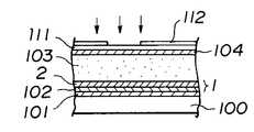
다음에, 상기한 바와같은 스핀트형의 FEC 제조과정의 일예를 도 5에 도시하는 모식도를 참조하여 설명한다. 우선, 도 5(a)에 도시하는 바와같이, 글라스 등의 기판(100)상에 스패터링 공정으로 캐소드 전극층의 재료인 Nb(니오뮴)막을 형성하여 박막 도체층(101)을 형성하고, 그 박막 도체층(101)상에 불순물을 도핑한 α-Si(비정질 실리콘) 막을 CVD (Chemical Vapor Deposition)로 형성하여 저항층(102)을 형성하고, 더나아가 저항층(102)상에 SiO2(이산화실리콘) 막을 CVD에 의하여 형성하여 절연층(103)을 형성한다. 그리고, 그 절연층(103)상에 게이트 전극층(104)을 이루는 Nb 막을 스패터링에 의하여 형성하여 적층 기판을 형성한다.Next, an example of the above-described spin type FEC manufacturing process will be described with reference to the schematic diagram shown in FIG. First, as shown in Fig. 5 (a), a thin
더욱, 그 적층기판의 최상표면인 게이트 전극층(104)상에 포토레지스트층(11)을 도포한 후, 마스크(112)를 형성하여 포토리소그래피 법으로 포토레지스트층(111)의 패터닝을 행하고, 포토레지스트층(111)에 개구패턴을 형성한다.Furthermore, after applying the photoresist layer 11 on the
다음에, SF6등의 가스를 사용하여, 포토레지스트층(111)이 도포되어 있는 방향에서 반응성 이온에칭(RIE)으로 이방성 에칭함으로써, 동도(b)에 도시하는 바와 같은 게이트 전극층(104)에 포토레지스트층(111)의 패턴과 동일한 개구부(113)를 제작한다.Next, by anisotropic etching with reactive ion etching (RIE) in the direction where the
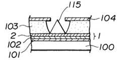
다음에 드라이 에칭에 의하여, 절연층(103) 부분을 이방성 에칭함으로써, 동도(c)에 도시하는 바와같이 절연층(103)에 홀(114)을 형성한다. 그리고, 그 적층기판을 동일 평면내에서 회전시키면서 박리층(105)으로 되는 Al(알루미늄)을 경사지게 증착하면, Al은 홀(114)중에 증착되지 않고, 동도(c)에 도시하는 바와 같이 게이트전극층(104)의 표면에만 선택적으로 부착하여 박리층(105)을 형성한다.Next, by dry etching, the portion of the
다음에, 이와같은 기판의 홀(114)측에 이미터 재료인 Mo(몰리브덴)를 증착공정에 의하여 퇴적시키면, 동도(d)에 도시하는 바와 같이 증착된 Mo가 홀(114)의 저변, 즉, 저항층(102) 상에 증착 및 퇴적함과 동시에 박리층(105) 상에도 이미터재료(106)인 Mo가 퇴적한다. 그리고, 그 박리층(105)상에 퇴적하는 이미터재료(106)에 의하여 개구부가 폐쇄됨과 동시에, 저항층(102)상에 콘(cone)형상의 이미터(이하,「이미터콘」이라함)(115)가 형성된다.Next, when Mo (molybdenum), which is an emitter material, is deposited on the
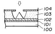
그후, 박리층(105)의 용해액인 인산에 기판을 담금으로써, 게이트 전극층(104)상의 박리층(105) 및 이미터재료(106)를 제거한다. 그결과, 동도면(e)에 도시하는 바와 같은 형상의 FEC를 얻을 수 있다.Thereafter, the substrate is immersed in phosphoric acid, which is a solution of the
또한, 도 4에 도시한 바와 같이, 저항층(102)상에 이미터콘(115)이 형성되어 있는 경우는 캐소드 전극층(101)의 캐소드 배선과 각 이미터콘(115) 사이의 거리에 따라, 캐소드 배선과 각 이미터콘(115) 사이의 저항치가 달라진다. 즉, 캐소드 배선의 근접위치에 형성되어 있는 이미터콘(115)에 대하여는 저항치가 낮아지고, 이미터콘 군의 중앙부에 형성되어 있는 캐소드배선으로 부터 원거리에 있는 이미터콘에 대하여는 저항치로 높아진다. 따라서, 캐소드배선의 근방에 위치하는 저항치가 낮은 이미터콘(115)으로 부터의 전자의 이미션 양은 증가하지만, 중앙부에 위치하는 이미터콘(115)으로 부터의 전자의 이미션 양은 감소하므로, 이미션 양은 불균일하게 된다.In addition, as shown in FIG. 4, when the
여기서, 이와같은 문제점을 해결하기 위하여 본 출원인이 앞서 일본 특원평 5-320923호에서 제안한 캐소드의 구조가 섬형상인 FEC의 일예를 도 6에 단면도로 도시한다.Here, in order to solve such a problem, an example of FEC in which the structure of the cathode proposed by the present applicant in Japanese Patent Application Laid-open No. Hei 5-320923 has an island shape is shown in sectional view in FIG.
이 경우, 캐소드배선(121)의 영역상에 도려낸 부를 설치하고, 그 내부에 캐소드 배선(121)로부터 분리된 섬형상 캐소드전극(122)을 형성하고, 그 섬형상 캐소드전극(122)에 대응하는 부분상에 1그룹 단위의 복수개의 이미터콘(126)을 형성한다. 이로써, 캐소드배선(121)과 1그룹을 구성하는 각 이미터콘(126)과의 사이의 저항치를 균일하게 할 수 있고, 각 이미터콘(126)으로 부터의 이미션 량을 균일한 것으로 할 수 있다.In this case, an indented portion is provided on the region of the
그런데, 도 4에 도시한 바와 같은 FEC에 있어서는 사용하는 외부 환경의 온도가 상승하면, α-Si로 이루어지는 저항층(102)의 저항치가 작아지고, 이미터콘(115)으로부터 출력되는 이미션 전류가 증가하기 때문에, 특히 온도변화가 큰 차재용 기기에 이와같은 FEC로 이루어지는 표시장치를 설치하면 좋지 않은 상태가 발생하는 문제점이 있었다.By the way, in FEC as shown in FIG. 4, when the temperature of the external environment to be used increases, the resistance value of the
또, 이와같은 FEC의 제조공정에 있어서는 도 5(c)에 도시한 바와 같이 드라이 에칭에 의하여 절연층(103)에 홀(114)를 형성하면, α-Si로 이루어지는 저항층(102)의 일부도 에칭된다.In the FEC manufacturing step, when the
이 때문에, α-Si로 이루어지는 저항층(102)의 표면이 변질되고, 그 저항층(102)상에 형성되는 이미터콘(115)과 저항층(102)의 밀착의 불량이 발생하여, 이미터콘(115)이 쉽게 박리되는 문제점이 있었다.For this reason, the surface of the
또, 도 6에 도시한 섬형상 캐소드 구조로 되는 FEC에 있어서는 전계 방출 특성이 이미터콘(126)과 섬형상 캐소드 전극(122) 사이의 저항치 및 섬형상 캐소드 전극(122)과 캐소드 배선(121) 사이의 저항치에 의하여 제어된다.In the FEC having the island-shaped cathode structure shown in FIG. 6, the field emission characteristics are the resistance value between the
즉, 이미터콘(126)과 섬형상 캐소드전극(122) 사이의 저항치가 작으면, 이미터콘(126)으로부터 방사되는 이미션 전류의 균일성이 손상되고, 이미터콘(126)과 섬형상 캐소드전극(122) 사이의 저항치가 크면, 인출전극인 게이트 전극(125)의 전압이 높아진다.That is, if the resistance between the
여기서, 저항층(123)을 비저항이 높은 저항층 재료로 형성하여 이미터콘(126)과 캐소드전극(122) 사이의 저항치를 크게 함과 동시에, 캐소드배선(121)과 섬형상 캐소드 전극(122) 사이의 캡을 작게하여 캐소드 배선(121)과 섬형상 캐소드 전극(122) 사이의 저항치를 작게하는 방법이 제안되어 있지만, 미세가공이 필요하게 되고, 제조공정이 복잡하게 되는 문제점도 있었다.Here, the
또, 저항층(123)의 막두께를 두껍게 한 경우도, 저항층(123)의 비저항을 크게한 경우와 동일한 효과를 얻을 수 있지만, 절연층(124) 및 게이트 전극층(125)등의 스텝 커버리지 특성 등으로 인하여 제조가 매우 곤란한 결점이 있었다.In addition, in the case where the thickness of the
도 1은 본 발명의 제1실시형태인 전계방출 캐소드의 일예를 도시한 도면이다.1 is a diagram showing an example of a field emission cathode as a first embodiment of the present invention.
도 2는 본 발명의 제1실시형태인 전계방출 캐소드의 제조방법의 일예를 도시한 도면이다.FIG. 2 is a diagram showing an example of a method of manufacturing a field emission cathode according to the first embodiment of the present invention.
도 3은 본 발명의 제2의 실시형태인 섬형상의 전계방출 캐소드의 일예를 도시한 도면이다.FIG. 3 is a diagram showing an example of an island-like field emission cathode that is a second embodiment of the present invention. FIG.
도 4는 FEC 어레이를 사용하는 표시장치의 설명도이다.4 is an explanatory diagram of a display device using an FEC array.
도 5는 종래의 전계방출 캐소드의 제조방법의 일례를 도시한 도면이다.5 is a view showing an example of a conventional method for producing a field emission cathode.
도 6은 종래의 섬형상의 전계방출 캐소드의 일예를 도시한 도면이다.6 is a diagram showing an example of a conventional island-shaped field emission cathode.
<도면의 주요부분에 대한 부호의 설명><Description of the code | symbol about the principal part of drawing>
1, 13: 저항층2, 15: 제2의 저항층1, 13:
11: 캐소드 배선12: 섬형상 캐소드 도체11: cathode wiring 12: island-shaped cathode conductor
14, 102: 제1의 저항층16, 103: 절연층14, 102: first
17, 104: 게이트 전극층18, 115: 이미터콘100: 기판17, 104: gate electrode layers 18, 115: emitter cone 100: substrate
101: 캐소드 전극층114: 홀101
본 발명은 이와같은 문제점을 해결하기 위하여 이루어진 것으로, 제1의 전계방출 캐소드로서, 기판상에 캐소드 전극층, 저항층, 절연층 및 게이트 전극층의 막을 차례로 형성한 적층기판에 대하여, 상기 게이트 전극층 및 상기 절연층에 홀이 설치되고, 그 홀내에 이미터가 형성되는 전계방출 캐소드에 있어서, 저항층은 적어도 온도 특성이 다른 2층 이상의 복수층의 저항층 재료로 형성한다.SUMMARY OF THE INVENTION The present invention has been made to solve such a problem, and is a first field emission cathode, and has a gate electrode layer and the gate layer of a laminated substrate in which a cathode electrode layer, a resistive layer, an insulating layer, and a gate electrode layer are sequentially formed on a substrate. In a field emission cathode in which a hole is provided in an insulating layer and an emitter is formed in the hole, the resistance layer is formed of at least two or more layers of resistance layer materials having different temperature characteristics.
또한, 저항층의 최상층을 드라이 에칭에 대하여 내성을 갖는 저항층 재료로 형성한다.Further, the uppermost layer of the resistive layer is formed of a resistive layer material resistant to dry etching.
또한 제2의 전계방출 캐소드로서, 캐소드배선의 영역내에 캐소드배선에서 분리된 복수의 캐소드 도체를 설치하고, 그 캐소드 배선과 캐소드 도체상에 저항층, 절연층 및 게이트 전극층의 막을 차례로 형성한 적층기판에 대하여, 상기 게이트 전극층 및 상기 절연층에 홀이 설치되고, 홀내에 이미터가 형성되는 전계 방출 캐소드에 있어서, 저항층이 적어도 비저항이 다른 2층 이상의 저항층 재료로 형성되도록 구성한다.In addition, as a second field emission cathode, a plurality of cathode conductors separated from the cathode interconnection are provided in the region of the cathode interconnection, and a laminated substrate in which a film of a resistive layer, an insulation layer, and a gate electrode layer is sequentially formed on the cathode interconnection and the cathode conductor. In the field emission cathode in which holes are provided in the gate electrode layer and the insulating layer, and emitters are formed in the holes, the resistive layer is configured to be formed of at least two resistive layer materials having different resistivities.
또한, 저항층의 최상층을 드라이 에칭에 대하여 내성을 갖고, 동시에 온도 특성이 다른 저항층 재료로 형성한다.Further, the uppermost layer of the resistive layer is formed of a resistive layer material having resistance to dry etching and at the same time having different temperature characteristics.
또한, 적어도 기판상에 캐소드 전극층, 최상층이 드라이 에칭에 대하여 내성을 갖는 저항층 재료로 이루어지는 복수의 저항층, 절연층 및 게이트전극층 막을 차례로 형성하여 적층 기판을 형성하고, 그 적층기판의 게이트전극층 및 절연층에 드라이 에칭법에 의하여 홀을 형성하는 공정과 홀내에 이미터를 형성하는 공정을 수행한다.Further, a plurality of resistive layers, insulating layers and gate electrode layer films formed of at least a cathode electrode layer and an uppermost layer of a resistive layer material resistant to dry etching are sequentially formed on the substrate to form a laminated substrate, and the gate electrode layer of the laminated substrate and A process of forming a hole in the insulating layer by a dry etching method and a process of forming an emitter in the hole are performed.
본 발명의 제1의 전계방출 캐소드에 의하면, 저항층을 적어도 2층 이상의 온도 특성이 다른 복수의 저항층재료에 의하여 형성하고 있기 때문에, 주위의 온도가 상승한 경우에도 저항층 전체의 저항치의 변화를 최소로 억제하고, 온도변화에 의한 이미션 전류의 증가를 감소시킬 수 있다.According to the first field emission cathode of the present invention, since the resistance layer is formed of a plurality of resistance layer materials having different temperature characteristics of at least two or more layers, the resistance value of the entire resistance layer is changed even when the ambient temperature rises. It can be suppressed to the minimum and the increase of the emission current due to the temperature change can be reduced.
또, 본 발명의 제2의 전계방출 캐소드에 의하면, 저항층을 적어도 비저항이 다른 2층 이상의 복수의 저항층 재료로 형성하고 있기 때문에, 캐소드 도체와 상기 이미터 사이의 저항치를 캐소드도체와 캐소드배선 사이의 저항치 보다 크게할 수 있다.In addition, according to the second field emission cathode of the present invention, since the resistance layer is formed of at least two or more resistance layer materials having different resistivities, the resistance between the cathode conductor and the emitter is reduced between the cathode conductor and the cathode wiring. It can be larger than the resistance between.
또, 본 발명의 전계방출 캐소드의 제조방법에 의하면, 저항층으로서 복수의 저항층 재료를 차례로 막으로 형성하고, 최상층을 드라이 에칭에 대하여 내성을 갖는 저항층 재료로 형성하였기 때문에, 모든 에칭공정을 드라이 에칭으로 행할 수 있다.In addition, according to the method for producing a field emission cathode of the present invention, since a plurality of resistive layer materials are sequentially formed as a film as a resistive layer, and the uppermost layer is formed of a resistive layer material resistant to dry etching, all the etching steps are performed. It can be performed by dry etching.
(발명 실시의 형태)(Invention embodiment)
도 1에 본 발명 실시형태인 전계방출 캐소드의 단면도의 일예를 도시한다.An example of sectional drawing of the field emission cathode which is embodiment of this invention in FIG. 1 is shown.
이 도면에 도시하는 전계방출 캐소드에는 글라스기판(100)상에 Nb 등으로 이루어지는 캐소드 전극층(101)막이 형성되고, 그 캐소드전극층(101)상에 예를들면 불순물을 도핑한 α-Si (비결정질 실리콘)등으로 이루어지는 제1의 저항층(102) 막이 형성되고, 그 제1의 저항층(102)상에는 제1의 저항층(102)과 온도 특성이 다른 Cr2O3(산화크롬)등으로 이루어지는 제2의 저항층(2)막이 형성되어 있다. 즉 α-Si 등으로 이루어지는 제1의 저항층(102)과 Cr2O3등으로 이루어지는 제2의 저항층(2)의 2층 구조로 저항층(1)이 형성되어 있다.In the field emission cathode shown in this figure, a
제2의 저항층(2)상에는 SiO2(이산화실리콘)으로 이루어지는 절연층(103)이 형성되어 있고 동시에, 그 절연층(103)에는 홀(114)이 설치되어 있고, 그 홀(114)의 저면, 즉 제2의 저항층(2)상에는 고 용융점 금속재료, 카아본재료 또는 질화물, 규소화합물, 탄화물 등으로 이루어지는 이미터콘(115)이 형성되어 있다. 또한 절연층(103)상에는 Nb로 이루어지는 게이트 전극층(104)이 형성되어 있다.An insulating
즉, 이와같이 본 발명의 실시의 형태인 FEC에 있어서는 저항층(1)을 α-Si로 이루어지는 제1의 저항층(102)과 제1의 저항층(102)과 온도특성이 다른 Cr2O3등으로 이루어지는 제2의 저항층(2)에 의하여 형성하도록 하고 있다.That is, in FEC according to the embodiment of the present invention, Cr2 O3 having different temperature characteristics from the
또한 저항층(1) 전체의 저항치는 제1의 저항층(102) 및 제2의 저항층(2)의 비저항을 고려하여, 제1의 저항층(102), 또는 제2의 저항층(2)의 막두께를 변화시켜, 소정의 저항치로 되도록 하고 있다.In addition, the resistance value of the
따라서, 주위의 온도가 상승하고, 제1의 저항층(102)의 저항치가 작아진 경우에도, 제2의 저항층(2)의 저항치가 크게 되기 때문에, 저항층(1) 전체의 온도변화에 의한 저항치의 변화를 최소로 억제할 수 있고, 이미터콘(115)으로부터 방사되는 이미션 전류의 증가를 억제할 수 있다.Therefore, even when the surrounding temperature rises and the resistance value of the
더욱이 제2의 저항층(2)의 저항재료로서는 Cr2O3외에, 예를들면 TaN (질화탄탈), Ta2N (질화이탄탈), SrO2(이산화스트론튬), Cr-SiO, SnO2(이산화주석), RuO2(이산화루테늄), Ni-Cr (니켈-크롬) 화합물, Zn-Ti-Ni (아연-티탄-니켈) 산화물, BaTiO3계의 화합물을 사용하는 것도 가능하다.Further, as the resistive material of the second
다음에, 이와같은 본 발명의 실시형태인 FEC의 제조과정을 제2의 모식도를 참조하여 설명하다. 우선, 도 2(a)에 도시하는 바와같이, 글라스 등의 기판(100)상에 스패터링공정으로, 예를들면 캐소드 재료인 Nb 등의 막을 형성하여 캐소드 전극층(101)을 형성하고, 그 캐소드 전극층(101)상에 불순물을 도핑한 α-Si등의 Si (실리콘)계의 재료로 이루어지는 제1의 저항층(102)막을 형성하고, 더나아가 그 저항층(102)상에 Cr2O3등으로 이루어지는 제2의 저항층(2)막을 CVD에 의해 형성하여 저항층(1)을 형성하고 있다. 또한 Cr2O3등의 제2저항층(2)의 재료는 실리콘산화물이 에칭용 가스(예를들면 SF6, CHF3)등에 대하여 내성을 갖고 있다.Next, the manufacturing process of FEC which is such embodiment of this invention is demonstrated with reference to a 2nd schematic diagram. First, as shown in Fig. 2 (a), a
더욱이, 그 제2의 저항층(2)상에는 SiO2막이 CVD에 의하여 형성되어 절연층(103)이 형성되고, 그 절연층(103)상에 게이트 전극층(104)으로 되는 Nb등의 막을 스패터링공정에 의하여 형성하여 적층기판을 형성한다.Further, on the second
더욱이 그 적층기판의 최상표면인 게이트 전극층(104)상에 포토레지스트층(111)을 도포한 후, 마스크(112)을 걷어내고 포토리소그래피법으로 레지스트층(111)의 패터닝을 행하고, 포토레지스트층(111)에 개구패턴을 형성한다.Furthermore, after applying the
다음에, SF6등의 가스를 사용하여, 포토레지스트층(111)이 도포되어 있는 방향에서 반응성 이온에칭(RIE)으로 이방성 에칭함으로써, 동도(b)에 도시하는 바와 같은 게이트 전극층(104)에 포토레지스트층(111)의 패턴과 동일한 개구부(113)를 제작하고, 이 개구부(113)가 설치된 기판을 CHF3+O2등에 의하여 드라이에칭하여 절연층(103) 부분을 이방성 에칭한다.Next, by anisotropic etching with reactive ion etching (RIE) in the direction where the
이로써, 동도(C)에 도시하는 바와 같이, 절연층(103)에 홀(114)이 형성된다. 그 기판을 동일 평면내에서 회전시키면서 박리층(105)으로 되는 Al (알루미늄), Ni (니켈) 등을 경사지게 증착함으로써, 박리층(115)은 홀(114)중에 증착되지 않고, 게이트 전극층(104)의 표면에만 선택적으로 부착되게 한다.Thereby, the
그리고, 이와같은 기판의 홀(114)의 저면, 즉, 제2의 저항층(2)상에 이미터재료로서, 고용융점 금속재료인 Mo (몰리브덴)를 증착에 의하여 퇴적시키면, 동도(α)에 도시하는 바와같이 증착된 Mo가 제2의 저항층(2)상에 증착 및 퇴적됨과 동시에, 박리층(105)상에도 퇴적된다. 그리고, 그 박리층(105)상에 퇴적하는 이미터 재료(106)에 의하여 개구부가 폐쇄됨과 동시에, 저항층(2)상에 콘형상의 이미터(115)가 형성된다. 그후, 박리층(105)의 용해액인 인산에 기판을 담금으로써, 게이트 전극층(104)상의 박리층(105), 및 이미터 재료(106)를 제거하고, 동도(e)에 도시하는 바와같은 형상의 FEC를 얻을 수 있다.When Mo (molybdenum), a high melting point metal material, is deposited as an emitter material on the bottom surface of the
이와같은 본 실시형태인 FEC의 제조공정에서는 저항층(1)의 최상층이 드라이에칭에 대하여 내성을 갖는 제2의 저항층(2)막으로 형성된다.In the FEC manufacturing process of this embodiment as described above, the uppermost layer of the
따라서, 드라이 에칭에 의하여 절연층(103)에 홀(114)을 형성한 경우에도 Cr2O3로 이루어지는 제2의 저항층(2)이 스톱층으로 되고 α-Si 등으로 이루어지는 제1의 저항층(102)의 표면의 변질이 방지되고, 모든 에칭공정을 드라이 에칭으로 행할 수 있다.Therefore, even when the
다음에, 본 발명의 제2의 실시형태인 섬형상 캐소드 구조의 FEC의 일예를 도 3에 도시한다.Next, FIG. 3 shows an example of the FEC of the island-like cathode structure which is the second embodiment of the present invention.
이 도면에 도시하는 전계방출 캐소드는 절연기판(100)상에 캐소드 배선(11)과 섬형상 캐소드 도체(12)가 Nb, Mo, Al 등의 도전성 박막으로 패턴형성되어 있고, 그 섬형상 캐소드 도체(12)와 캐소드 배선(11)상에는 α-Si 등으로 이루어지는 제1의 저항층(14)이 캐소드 배선(11)의 영역내 전면에 막으로 형성되고, 더욱이 제1의 저항층(14)상에 Cr2O3등으로 이루어지는 제2의 저항층(15)막이 형성되어 저항층(13)을 형성하고 있다.The field emission cathode shown in this figure is formed on the insulating
여기서, 제2의 저항층(15)의 비저항(ρ2)이 제1의 저항층(14)의 비저항(ρ1) 보다도 크게 되도록하는 저항층 재료가 사용된다.Here, a resistive layer material is used so that the specific resistance ρ2 of the second
더욱이, 제2의 저항층(15)상에 SiO2로 이루어지는 절연층(16) 및 Nb, Mo, Al, WSi2등으로 이루어지는 게이트 전극층(17)이 형성되고, 그 게이트 전극층(17)과 절연층(16)에 개구부가 설치되어 있다. 그리고 그 개구부의 섬형상 캐소드 도체(12)에 대응하는 저항층(13)상에 1그룹 단위의 복수개의 이미터콘(18)이 형성되어 있다.Furthermore, an insulating
이와같이 저항층(13)을 제1의 저항층(14)과 제2의 저항층(15)의 2층 구조로 하고, 제1의 저항층(14)의 비저항(ρ1)을 제2의 저항층(15)의 비저항(ρ2) 보다도 작은 것으로 함으로써, 이미터콘(18)과 섬형상 캐소드 도체(12) 사이의 저항치를 크게할 수 있어, 이미터콘(18)으로부터 방사되는 이미션 전류를 균일하게 유지할 수 있음과 동시에, 섬형상 캐소드 도체(12)와 캐소드 배선(11) 사이의 저항치는 제1의 저항층(14)의 비저항과 거의 같거나 작게 유지할 수 있기 때문에, 게이트 전극층(17)의 인출전압을 높이할 필요가 없다.Thus, the
더욱이, 주위의 온도가 상승한 경우에도 저항층(13)이 α-Si로 이루어지는 제1의 저항층(14)과 그 저항층(14)과 저항의 온도특성이 다른 Cr2O3로 이루어지는 제2의 저항층(15)에 의하여 형성되어 있기 때문에, 전체적으로는 온도변화에 의한 저항치의 변화를 최소로 억제함과 동시에 저항층(14)의 최상층이 드라이 에칭에 대하여 내성을 갖는 저항층재료이기 때문에, 모든 에칭공정을 드라이 에칭으로 행할 수 있는 이점도 있다.Furthermore, even when the ambient temperature rises, the
더욱이, 본 발명의 실시형태에서는 저항층을 제1의 저항층과 제2의 저항층으로 이루어지는 2층 구조로 한 경우에 대하여 설명하였지만, 저항층의 비저항을 조정하기 위하여, 더욱 다층구조로 하여도 좋다.Furthermore, in the embodiment of the present invention, the case where the resistive layer has a two-layer structure composed of the first resistive layer and the second resistive layer has been described. However, in order to adjust the resistivity of the resistive layer, the multilayered structure may be used. good.
이상 설명한 바와 같이, 본 발명의 제1의 전계방출 캐소드에 의하면, 저항층을 적어도 온도특성이 다른 복수의 저항층 재료에 의하여 형성하고 있기 때문에, 주위의 온도가 상승한 경우에도 저항층 전체의 저항치의 변화를 최소로 억제할 수 있으므로, 온도변화에 의한 이미션 전류의 변동을 방지할 수 있게 된다.As described above, according to the first field emission cathode of the present invention, since the resistance layer is formed of at least a plurality of resistance layer materials having different temperature characteristics, even when the ambient temperature rises, the resistance value of the entire resistance layer is increased. Since the change can be suppressed to a minimum, the fluctuation in the emission current due to the temperature change can be prevented.
또한, 본 발명의 제2전계방출 캐소드에 의하면, 저항층을 적어도 비저항이 다른 2층 이상의 복수의 저항층 재료로 형성하고, 캐소드 도체와 이미터 사이의 저항치가 캐소드 배선과 캐소드 도체 사이의 저항치 보다 크게 되어 있기 때문에, 게이트 전극층의 인출전압을 상승시키지 않고 이미션 전류를 균일하게 유지할 수 있는 이점이 있다.Further, according to the second field emission cathode of the present invention, the resistance layer is formed of a plurality of resistance layer materials of at least two layers having different specific resistances, and the resistance value between the cathode conductor and the emitter is larger than the resistance value between the cathode wiring and the cathode conductor. Since it is large, there is an advantage that the emission current can be kept uniform without raising the withdrawal voltage of the gate electrode layer.
또한, 본 발명의 제조방법에 의하면 저항층의 최상층이 드라이 에칭에 대하여 내성을 갖는 저항층 재료로 형성되어 있기 때문에, 모든 에칭공정을 드라이 에칭으로 행할 수 있고, 제조공정의 간략화 및 안정화를 도모할 수 있다.In addition, according to the manufacturing method of the present invention, since the uppermost layer of the resistive layer is formed of a resistive layer material resistant to dry etching, all the etching processes can be performed by dry etching, and the manufacturing process can be simplified and stabilized. Can be.
Claims (7)
Translated fromKoreanApplications Claiming Priority (2)
| Application Number | Priority Date | Filing Date | Title |
|---|---|---|---|
| JP4563496AJPH09219144A (en) | 1996-02-08 | 1996-02-08 | Electric field emitting cathode and its manufacture |
| JP96-045634 | 1996-02-08 |
Publications (2)
| Publication Number | Publication Date |
|---|---|
| KR970063321A KR970063321A (en) | 1997-09-12 |
| KR100235212B1true KR100235212B1 (en) | 1999-12-15 |
Family
ID=12724803
Family Applications (1)
| Application Number | Title | Priority Date | Filing Date |
|---|---|---|---|
| KR1019970003686AExpired - Fee RelatedKR100235212B1 (en) | 1996-02-08 | 1997-02-06 | A field emission cathode and maunfacture thereof |
Country Status (5)
| Country | Link |
|---|---|
| US (1) | US5892321A (en) |
| JP (1) | JPH09219144A (en) |
| KR (1) | KR100235212B1 (en) |
| FR (1) | FR2744834B1 (en) |
| TW (1) | TW416073B (en) |
Families Citing this family (17)
| Publication number | Priority date | Publication date | Assignee | Title |
|---|---|---|---|---|
| JPH10340666A (en)* | 1997-06-09 | 1998-12-22 | Futaba Corp | Field electron emission element |
| US6013986A (en)* | 1997-06-30 | 2000-01-11 | Candescent Technologies Corporation | Electron-emitting device having multi-layer resistor |
| KR100334017B1 (en)* | 1999-03-18 | 2002-04-26 | 김순택 | A flat panel display |
| US7052350B1 (en)* | 1999-08-26 | 2006-05-30 | Micron Technology, Inc. | Field emission device having insulated column lines and method manufacture |
| KR100480771B1 (en)* | 2000-01-05 | 2005-04-06 | 삼성에스디아이 주식회사 | Field emission device and the fabrication method thereof |
| KR100464314B1 (en)* | 2000-01-05 | 2004-12-31 | 삼성에스디아이 주식회사 | Field emission device and the fabrication method thereof |
| US6424083B1 (en) | 2000-02-09 | 2002-07-23 | Motorola, Inc. | Field emission device having an improved ballast resistor |
| US6392355B1 (en) | 2000-04-25 | 2002-05-21 | Mcnc | Closed-loop cold cathode current regulator |
| KR20020017594A (en)* | 2000-08-31 | 2002-03-07 | 구자홍 | Carbon nano tubefield emission device having resistance layer of cluster structure |
| US6611093B1 (en)* | 2000-09-19 | 2003-08-26 | Display Research Laboratories, Inc. | Field emission display with transparent cathode |
| US20030034721A1 (en)* | 2001-08-20 | 2003-02-20 | Henry Windischmann | Method for improving field emission uniformity from a carbon-based array |
| KR20050115057A (en)* | 2004-06-03 | 2005-12-07 | 삼성에스디아이 주식회사 | A long life-time field emitter for a field emission device and a method for fabricating the same |
| KR20060104654A (en)* | 2005-03-31 | 2006-10-09 | 삼성에스디아이 주식회사 | Electron emitting device and method for manufacturing same |
| KR100718992B1 (en)* | 2005-07-01 | 2007-05-16 | 엘지전자 주식회사 | Organic electroluminescent device and manufacturing method thereof |
| EP2826056B1 (en)* | 2012-03-16 | 2023-07-19 | Nano-X Imaging Ltd | X-ray emitting device |
| EP2885806A4 (en)* | 2012-08-16 | 2018-04-25 | Nanox Imaging Plc | Image capture device |
| KR102259859B1 (en) | 2013-11-27 | 2021-06-03 | 나녹스 이미징 피엘씨 | Electron emitting construct configured with ion bombardment resistant |
Family Cites Families (8)
| Publication number | Priority date | Publication date | Assignee | Title |
|---|---|---|---|---|
| FR2623013A1 (en)* | 1987-11-06 | 1989-05-12 | Commissariat Energie Atomique | ELECTRO SOURCE WITH EMISSIVE MICROPOINT CATHODES AND FIELD EMISSION-INDUCED CATHODOLUMINESCENCE VISUALIZATION DEVICE USING THE SOURCE |
| US4990766A (en)* | 1989-05-22 | 1991-02-05 | Murasa International | Solid state electron amplifier |
| FR2650119A1 (en)* | 1989-07-21 | 1991-01-25 | Thomson Tubes Electroniques | Individual current regulating device for a tip in a field-effect microcathode planar array, and method of production |
| FR2663462B1 (en)* | 1990-06-13 | 1992-09-11 | Commissariat Energie Atomique | SOURCE OF ELECTRON WITH EMISSIVE MICROPOINT CATHODES. |
| JP2699827B2 (en)* | 1993-09-27 | 1998-01-19 | 双葉電子工業株式会社 | Field emission cathode device |
| US5451830A (en)* | 1994-01-24 | 1995-09-19 | Industrial Technology Research Institute | Single tip redundancy method with resistive base and resultant flat panel display |
| US5502347A (en)* | 1994-10-06 | 1996-03-26 | Motorola, Inc. | Electron source |
| US5557159A (en)* | 1994-11-18 | 1996-09-17 | Texas Instruments Incorporated | Field emission microtip clusters adjacent stripe conductors |
- 1996
- 1996-02-08JPJP4563496Apatent/JPH09219144A/ennot_activeWithdrawn
- 1997
- 1997-01-30USUS08/791,744patent/US5892321A/ennot_activeExpired - Fee Related
- 1997-01-30TWTW086101039Apatent/TW416073B/ennot_activeIP Right Cessation
- 1997-02-06KRKR1019970003686Apatent/KR100235212B1/ennot_activeExpired - Fee Related
- 1997-02-07FRFR9701413Apatent/FR2744834B1/ennot_activeExpired - Fee Related
Also Published As
| Publication number | Publication date |
|---|---|
| JPH09219144A (en) | 1997-08-19 |
| TW416073B (en) | 2000-12-21 |
| US5892321A (en) | 1999-04-06 |
| FR2744834B1 (en) | 2006-10-06 |
| FR2744834A1 (en) | 1997-08-14 |
| KR970063321A (en) | 1997-09-12 |
Similar Documents
| Publication | Publication Date | Title |
|---|---|---|
| KR100235212B1 (en) | A field emission cathode and maunfacture thereof | |
| US6144144A (en) | Patterned resistor suitable for electron-emitting device | |
| US5828163A (en) | Field emitter device with a current limiter structure | |
| US5578896A (en) | Cold cathode field emission display and method for forming it | |
| EP0503638B1 (en) | Array of field emission cathodes | |
| US6607930B2 (en) | Method of fabricating a field emission device with a lateral thin-film edge emitter | |
| US5394006A (en) | Narrow gate opening manufacturing of gated fluid emitters | |
| KR100225561B1 (en) | Field emission type electron source | |
| KR100618531B1 (en) | Electron emission device, electron source, and image display having dipole layer | |
| US5378182A (en) | Self-aligned process for gated field emitters | |
| KR100243990B1 (en) | Field emission cathode and method for manufacturing the same | |
| JP3246137B2 (en) | Field emission cathode and method of manufacturing field emission cathode | |
| JP3066573B2 (en) | Field emission display device | |
| US5789272A (en) | Low voltage field emission device | |
| JPH06162919A (en) | Field emission cold cathode element | |
| JP2737618B2 (en) | Field emission type electron source | |
| US7030545B2 (en) | Field emission cathode with emitters formed of acicular protrusions with secondary emitting protrusions formed thereon | |
| US5787337A (en) | Method of fabricating a field-emission cold cathode | |
| US7071603B2 (en) | Patterned seed layer suitable for electron-emitting device, and associated fabrication method | |
| US5650689A (en) | Vacuum airtight device having NbN electrode structure incorporated therein | |
| JP3526462B2 (en) | Field emission type cathode device | |
| JP2852356B2 (en) | Field emitter surface modification method | |
| US7053538B1 (en) | Sectioned resistor layer for a carbon nanotube electron-emitting device | |
| US5874808A (en) | Low turn-on voltage volcano-shaped field emitter and integration into an addressable array | |
| JP2743794B2 (en) | Field emission cathode and method of manufacturing field emission cathode |
Legal Events
| Date | Code | Title | Description |
|---|---|---|---|
| PA0109 | Patent application | St.27 status event code:A-0-1-A10-A12-nap-PA0109 | |
| R17-X000 | Change to representative recorded | St.27 status event code:A-3-3-R10-R17-oth-X000 | |
| A201 | Request for examination | ||
| P11-X000 | Amendment of application requested | St.27 status event code:A-2-2-P10-P11-nap-X000 | |
| P13-X000 | Application amended | St.27 status event code:A-2-2-P10-P13-nap-X000 | |
| PA0201 | Request for examination | St.27 status event code:A-1-2-D10-D11-exm-PA0201 | |
| PG1501 | Laying open of application | St.27 status event code:A-1-1-Q10-Q12-nap-PG1501 | |
| E701 | Decision to grant or registration of patent right | ||
| PE0701 | Decision of registration | St.27 status event code:A-1-2-D10-D22-exm-PE0701 | |
| GRNT | Written decision to grant | ||
| PR0701 | Registration of establishment | St.27 status event code:A-2-4-F10-F11-exm-PR0701 | |
| PR1002 | Payment of registration fee | St.27 status event code:A-2-2-U10-U11-oth-PR1002 Fee payment year number:1 | |
| PG1601 | Publication of registration | St.27 status event code:A-4-4-Q10-Q13-nap-PG1601 | |
| PR1001 | Payment of annual fee | St.27 status event code:A-4-4-U10-U11-oth-PR1001 Fee payment year number:4 | |
| PR1001 | Payment of annual fee | St.27 status event code:A-4-4-U10-U11-oth-PR1001 Fee payment year number:5 | |
| PR1001 | Payment of annual fee | St.27 status event code:A-4-4-U10-U11-oth-PR1001 Fee payment year number:6 | |
| PN2301 | Change of applicant | St.27 status event code:A-5-5-R10-R13-asn-PN2301 St.27 status event code:A-5-5-R10-R11-asn-PN2301 | |
| PR1001 | Payment of annual fee | St.27 status event code:A-4-4-U10-U11-oth-PR1001 Fee payment year number:7 | |
| FPAY | Annual fee payment | Payment date:20060908 Year of fee payment:8 | |
| PR1001 | Payment of annual fee | St.27 status event code:A-4-4-U10-U11-oth-PR1001 Fee payment year number:8 | |
| LAPS | Lapse due to unpaid annual fee | ||
| PC1903 | Unpaid annual fee | St.27 status event code:A-4-4-U10-U13-oth-PC1903 Not in force date:20070922 Payment event data comment text:Termination Category : DEFAULT_OF_REGISTRATION_FEE | |
| PC1903 | Unpaid annual fee | St.27 status event code:N-4-6-H10-H13-oth-PC1903 Ip right cessation event data comment text:Termination Category : DEFAULT_OF_REGISTRATION_FEE Not in force date:20070922 |