KR100234914B1 - Optical displacement measurement device and optical displacement measurement system - Google Patents
Optical displacement measurement device and optical displacement measurement systemDownload PDFInfo
- Publication number
- KR100234914B1 KR100234914B1KR1019970073309AKR19970073309AKR100234914B1KR 100234914 B1KR100234914 B1KR 100234914B1KR 1019970073309 AKR1019970073309 AKR 1019970073309AKR 19970073309 AKR19970073309 AKR 19970073309AKR 100234914 B1KR100234914 B1KR 100234914B1
- Authority
- KR
- South Korea
- Prior art keywords
- light
- output
- modulation control
- signal
- displacement measuring
- Prior art date
- Legal status (The legal status is an assumption and is not a legal conclusion. Google has not performed a legal analysis and makes no representation as to the accuracy of the status listed.)
- Expired - Fee Related
Links
Images


Classifications
- G—PHYSICS
- G01—MEASURING; TESTING
- G01B—MEASURING LENGTH, THICKNESS OR SIMILAR LINEAR DIMENSIONS; MEASURING ANGLES; MEASURING AREAS; MEASURING IRREGULARITIES OF SURFACES OR CONTOURS
- G01B11/00—Measuring arrangements characterised by the use of optical techniques
- G01B11/02—Measuring arrangements characterised by the use of optical techniques for measuring length, width or thickness
- G01B11/06—Measuring arrangements characterised by the use of optical techniques for measuring length, width or thickness for measuring thickness ; e.g. of sheet material
- G—PHYSICS
- G01—MEASURING; TESTING
- G01B—MEASURING LENGTH, THICKNESS OR SIMILAR LINEAR DIMENSIONS; MEASURING ANGLES; MEASURING AREAS; MEASURING IRREGULARITIES OF SURFACES OR CONTOURS
- G01B11/00—Measuring arrangements characterised by the use of optical techniques
- G—PHYSICS
- G01—MEASURING; TESTING
- G01C—MEASURING DISTANCES, LEVELS OR BEARINGS; SURVEYING; NAVIGATION; GYROSCOPIC INSTRUMENTS; PHOTOGRAMMETRY OR VIDEOGRAMMETRY
- G01C3/00—Measuring distances in line of sight; Optical rangefinders
- G01C3/02—Details
- G01C3/06—Use of electric means to obtain final indication
Landscapes
- Physics & Mathematics (AREA)
- General Physics & Mathematics (AREA)
- Electromagnetism (AREA)
- Engineering & Computer Science (AREA)
- Radar, Positioning & Navigation (AREA)
- Remote Sensing (AREA)
- Measurement Of Optical Distance (AREA)
- Length Measuring Devices By Optical Means (AREA)
Abstract
Translated fromKoreanDescription
Translated fromKorean본 발명은 물체를 비임 광(beam light)으로 조사하고(irradiating) 그 물체로부터 반사되는 광을 검출하여 3각 측량(triangulation)에 의해 그 물체까지의 거리와 그 물체의 기준 위치로부터의 변위를 검출하기 위한 광학 변위 측정 장치 및 광학 변위 측정 시스템에 관한 것이다.The present invention irradiates an object with beam light and detects the light reflected from the object to detect distance to the object and displacement from the reference position of the object by triangulation. An optical displacement measuring device and an optical displacement measuring system are provided.
지금 까지, 도 29에 도시된 바와 같이 레이져 다이오드(11)로부터 방사된(emitted) 적외선을 광 투과 렌즈를 통해 통과시키고 광 수신 광학 시스템의 광 수신 렌즈(22)를 통해 위치 검출 소자(21)에서 물체(3)으로부터 발산되어 반사된 광(diffused reflected light)을 수신함으로써 제공되는 비임 광을 사용하여 물체(3)을 조사하고(irradiate), 이에 의해 3각 측량의 원리를 적용하여 물체(3)의 위치 (또는 물체(3)의 기준 위치로부터의 변위)를 검출하는 광학 변위 측정 장치가 공지되어 왔다. 즉, 비임 광을 사용하여 물체(3)을 조사함으로써 물체(3)의 표면 상에 형성된 광 투과 스폿의 영상은 광 수신 스폿을 형성하기 위한 광 수신 렌즈(22)를 통해 위치 검출 소자(21)의 광 수신면(light reception face) 상에 형성되고, 물체(3)까지의 거리가 변함에 따라 광 수신 스폿 형성 위치가 변하는데, 이러한 사실이 물체(3)까지의 거리를 검출하는데 사용된다.Up to now, as shown in FIG. 29, the infrared rays emitted from the
레이져 다이오드(11)은 오실레이터(13)에 의해 출력되는 주파수 fA를 갖는 구동 신호에 의해 구동되고 LD 구동 회로를 통해 통과되어 변조된 레이져 광을 출력하므로 광 출력은 사인파와 같이 변한다.The
위치 검출 소자(21)은 길이 방향을 광 수신 스폿의 이동 방향과 정합시키기도록 배치된 PSD (위치 감지 장치) 또는 광 수신 스폿의 이동 방향으로 배치된 두 개의 다이오드를 사용한다. 핀 구조를 갖는 반도체 장치인 PSD는 광 수신면의 길이 방향의 양 단부에 제공된 한쌍의 전극과 공통 전극을 포함한다. 광 스폿이 광 수신 면상에 형성될 때, 양 단부의 전극 사이의 저항은 광 스폿의 위치에 따라 광 스폿의 위치에서 분할된다. 즉, 일정한 전류가 공통 전극으로부터 공급되고, 이에 의해 광 스폿의 위치에 따른 비율로 전류값을 갖는 위치 신호(11A 및 12A)가 양 단부에서 전극으로부터 출력된다. 광 스폿의 위치는 위치 신호(11A 및 12A) 사이의 비율에 상대적이므로, PSD의 수신면 상에 형성된 광 스폿의 위치는 (11A-12A)/(11A+12A) 또는 이의 보정된 값의 함수가 된다.The
위치 검출 소자(21)에 의해 출력되는 전기 신호의 위치 신호(11A 및 12A)는 I/V 변환 회로(23a 및 23b)에 의해 전압 신호로 변환되고 전압 신호는 증폭기(24a 및 24b)에 의해 증폭되어 검출 회로(25a 및 25b)에 의해 동기식으로(synchronously) 검출되며, 이에 의해 단지 신호 성분(Vd1A 및 Vd2A)만이 추출된다. 검출 회로(25a 및 25b)는 오실레이터(13)의 출력에 기초하여 타이밍 회로(28)에 의해 생성되는 타이밍 신호에 의해 검출 타이밍으로 제어된다. 이와 같이 추출된 신호 성분(Vd1A 및 Vd2A)은 (레이져 광이 변조될 때) 동일한 진동 파형(pulsation waveforms)이므로, 로우-패스 필터를 통해 검출 회로의 출력값의 평균을 구함으로써 제공되는 위치 정보신호(V1A 및 V2A)를 구하여 신호 레벨을 추출한다.The position signals 11A and 12A of the electrical signal output by the
위치 정보 신호(V1A 및 V2A)는 위치 신호(11A 및 12A)의 신호값에 비례하는 신호값을 갖는 전기 신호이므로, 만일 연산부(27)이(V1A-V2A)/(V1A+V2A)을 구하면, 물체(3)까지의 거리와 동등한 정보가 제공될 수 있다. 즉, 연산부(27)은(V1A-V2A) 을 계산하기 위한 차 연산부(27a)과 (V1A+V2A)을 계산하기 위한 합 연산부(27b)과 차 연산부(27a)의 출력 값을 합 연산부(27b)의 출력값으로 나누기 위한 나눗셈부(27c)로 구성된다. 합 연산부(27b)에 의해 계산된 (V1A+V2A)이 위치 검출 소자(21)의 모든 전류와 동등하고 광 수신량에 대응하므로, 아날로그 출력값은 정규화되어 물체(3)의 표면에서의 반사 계수의 차 또는 레이져 다이오드(11)에 의해 생성된 레이져 광의 강도차에 의해 야기되는 광 수신량의 변화는 연산부(27)에 의해 출력되는 값에 의해 영향을 받지 않는다. 이는 이상적으로 물체(3)까지의 거리는 광 수신량이 변하더라도 구할 수 있다는 것을 의미한다.Since the position information signals V1A and V2A are electrical signals having signal values proportional to the signal values of the position signals 11A and 12A, if the calculating
한편, 두 개의 광학 변위 측정 장치를 배치하기 위한 기술이 제안되었는데, 이하에서는 이를 간단히 변위 센서라고 부르기로 한다. 이 두 개의 광학 변위 측정 장치(1A 및 1B)는 서로 마주보게 배치되어 물체(3)의 두께를 측정하기 위해 물체(3)의 양 면까지의 거리를 측정한다. 즉, 두 개의 변위 센서(1A 및 1B)는 광 비임이 서로 반대 방향으로 형성되도록 배치되고, 변위 센서에서의 측정값은 그 사이의 거리로 감하여져(subtracted) 물체(3)의 두께를 구한다. 사실상, 공지된 두께를 갖는 기준 게이지 주위의 변위 센서(1A 및 1B)를 사용하여 얻은 측정값의 합에 기준 게이지의 두께가 합해져 보정 상수 α를 생성하는데, 이 값은 두 개의 변위 센서(1A 및 1B) 사이의 실질적인 거리와 동등하다. 측정되야 할 물체에 대하여 변위 센서(1A 및 1B)를 사용하여 측정된 거리(1A 및 1B)의 합은 보정 상수 α에 의해 감하여져 (a-(LA+LB)), 물체(3)의 두께가 구해질 수 있다.On the other hand, a technique for arranging two optical displacement measuring devices has been proposed, hereinafter referred to simply as a displacement sensor. These two optical displacement measuring
한편, 상술한 바와 같이 두 개의 변위 센서(1A 및 1B)이 물체(3)의 두께를 측정하기 위하여 사용되는 경우, 만일 물체(3)이 투명하지 않으면(nontranslucent) 두 개의 변위 센서(1A 및 1B)는 두께를 분리하여 측정하므로 문제가 생기지 않는다. 만일 물체(3)이 투명하다면, 양 변위 센서(1A 및 1B)는 서로 간섭하고 양호한 정확도로 두께를 측정할 수 없다. 예를 들어, 물체(3)이 종이, 세라믹 등이라면, 비임 광은 물체(3)의 내부에 도달한다. 그리하여, 두께가 작다면, 비임 광의 일부는 후방면으로 누설되고 반대편 변위 센서(1A, 1B)에서 수신된다. 여기서, 비임은 상술한 바와 같이 변조되고 통상적으로 그 사이에 위상차가 존재한다. 더욱이, 두 개의 변위 센서(1A 및 1B)의 특성을 완전히 정합시키는 것은 어렵다. 따라서, 또한 통상적으로 비임을 변조시키는 주파수(fA 및 fB) 사이에는 차이가 있다. 그러므로, 변위 센서(1A, 1B)에서 수신되는 광의 길이는 도 30에 도시된 바와 같이 주파수(fA 및 fB) 사이의 차이와 동일한 진동 주파수로 시간에 따라 변화한다. 시간 변화 진폭은 반사광과 투과광 사이의 비율에 따라 변화한다. 주파수(fA 및 fB) 사이의 변화는 여러 가지 이유로 야기되며, 이는 또한 회로 상수 변동, 온도 특성 변동 등에 의해 야기된다. 수신된 광 진폭 및 주파수는 유일하게 결정될 수 없다.On the other hand, when the two
그러므로, 그러한 진동 성분은 제거하기 어렵고 진동 성분은 연산부(27)의 입력에 포함된 즉, 연산부(27)으로 입력되는 위치 정보 신호(V1A 및 V2A) (및 변위 센서(1B)의 연산부(27)으로 입력되는 위치 정보 신호(V1B 및 V2B)는 진동 주파수로(at beat frequenly) 진폭이 변하고, 따라서 거리가 구하여졌을 때 분자 (V1A-V2A), (V1B-V2B)가 변하게 되며, 그 결과 측정 정확도 또는 해상도는 항상 시간에 따라 변한다.Therefore, such a vibration component is difficult to remove and the vibration component is included in the input of the
이상적으로, 거리는 광 수신량이 변하더라도 정합된다. 사실상, 연산부(27)로의 위치 검출 부분(21)의 처리는 비선형 부분을 포함한다. 그리하여, 만일 광 수신량의 시간 변화 진폭이 크면, 구한 거리가 변한다. 부재 회로(member circuits)의 몇몇은 포화되고, 거리 측정이 불가능해지거나 큰 오차가 생긴다.Ideally, the distance is matched even if the amount of light received varies. In fact, the processing of the
두 개의 변위 센서(1A 및 1B)의 비임이 물체(3)의 두께를 측정하기 위해 서로 간섭하는 예를 논의했다. 만일 다수의 변위 센서(1A 및 1B)가 그들이 서로 광 비임 간섭을 갖도록, 예를 들어 변위 센서(1A 및 1B)가 나란히 배치되어 광 투과 스폿이 위치 검출 소자(21)의 시야 내에서 형성되도록 배치되는 위치 관계로 제공되면, 간섭이 일어날 수 있는 가능성이 있다.An example where the beams of the two
그러므로, 본 발명의 목적은 서로 간섭하지 않고 거리를 측정하기 위한 광학 변위 측정 장치 및 이 광학 변위 측정 장치를 사용하는 광학 변위 측정 시스템을 제공하는 것이다.It is therefore an object of the present invention to provide an optical displacement measuring device for measuring distance without interfering with each other and an optical displacement measuring system using the optical displacement measuring device.
도 1은 본 발명의 제1 실시예를 도시하는 블록도.1 is a block diagram showing a first embodiment of the present invention.
도 2(a) 내지 도 2(k)는 본 발명의 제1 실시예의 동작을 설명하기 위한 도면.2 (a) to 2 (k) are diagrams for explaining the operation of the first embodiment of the present invention.
도 3은 본 발명의 제2 실시예를 도시하는 블록도.3 is a block diagram showing a second embodiment of the present invention;
도 4(a) 내지 도 4(l)은 본 발명의 제2 실시예의 동작을 설명하기 위한 도면.4 (a) to 4 (l) are diagrams for explaining the operation of the second embodiment of the present invention.
도 5(a) 내지 도 5(k)는 본 발명의 제3 실시예의 동작을 설명하기 위한 도면.5 (a) to 5 (k) are diagrams for explaining the operation of the third embodiment of the present invention.
도 6은 본 발명의 제4 실시예를 도시하는 블록도.6 is a block diagram showing a fourth embodiment of the present invention.
도 7(a) 내지 도 7(k)는 본 발명의 제4 실시예의 동작을 설명하기 위한 도면.7A to 7K are diagrams for explaining the operation of the fourth embodiment of the present invention.
도 8은 본 발명의 제5 실시예를 도시하는 블록도.8 is a block diagram showing a fifth embodiment of the present invention.
도 9(a) 내지 도 9(k)는 본 발명의 제5 실시예의 동작을 설명하기 위한 도면.9 (a) to 9 (k) are diagrams for explaining the operation of the fifth embodiment of the present invention.
도 10은 본 발명의 제6 실시예를 도시하는 블록도.10 is a block diagram showing a sixth embodiment of the present invention;
도 11(a) 내지 도 11(l)는 본 발명의 제6 실시예의 동작을 설명하기 위한 도면.11 (a) to 11 (l) are diagrams for explaining the operation of the sixth embodiment of the present invention.
도 12(a) 내지 도 12(k)는 본 발명의 제7 실시예의 동작을 설명하기 위한 도면.12 (a) to 12 (k) are diagrams for explaining the operation of the seventh embodiment of the present invention.
도 13은 본 발명의 제8 실시예를 도시하는 블록도.Fig. 13 is a block diagram showing an eighth embodiment of the present invention.
도 14(a) 내지 도 14(k)는 본 발명의 제8 실시예의 동작을 설명하기 위한 도면.14 (a) to 14 (k) are diagrams for explaining the operation of the eighth embodiment of the present invention.
도 15(a)는 본 발명의 제9 실시예를 도시하는 주요 부품 회로도.Fig. 15A is a main component circuit diagram showing a ninth embodiment of the present invention.
도 15(b) 내지 도 15(d)는 본 발명의 제9 실시예의 다른 하나의 실시예를 도시하는 도면.15 (b) to 15 (d) show another embodiment of the ninth embodiment of the present invention.
도 16(a) 내지 도 16(e)는 본 발명의 제9 실시예의 동작을 설명하기 위한 도면.16A to 16E are diagrams for explaining the operation of the ninth embodiment of the present invention.
도 17은 본 발명의 제10 실시예의 배치례(placement example)를 도시하는 도면.FIG. 17 is a diagram showing a placement example of the tenth embodiment of the present invention. FIG.
도 18은 본 발명의 제10 실시예를 도시하는 주요 부품 회로도.18 is a main component circuit diagram showing a tenth embodiment of the present invention.
도 19(a) 내지 도 19(f)는 본 발명의 제10 실시예의 동작을 설명하기 위한 도면.19 (a) to 19 (f) are diagrams for explaining the operation of the tenth embodiment of the present invention.
도 20은 본 발명의 제11 실시예의 배치예를 도시하는 도면.20 is a diagram showing an arrangement example of the eleventh embodiment of the present invention;
도 21(a) 내지 도 21(h)는 본 발명의 제11 실시예의 동작을 설명하기 위한 도면.21 (a) to 21 (h) are diagrams for explaining the operation of the eleventh embodiment of the present invention.
도 22는 본 발명의 제12 실시예를 도시하는 블록도.Fig. 22 is a block diagram showing the twelfth embodiment of the present invention.
도 23은 본 발명의 제13 실시예를 도시하는 블록도.Fig. 23 is a block diagram showing the thirteenth embodiment of the present invention.
도 24는 본 발명의 제14 실시예를 도시하는 블록도.24 is a block diagram showing a fourteenth embodiment of the present invention.
도 25는 본 발명의 제15 실시예를 도시하는 블록도.Fig. 25 is a block diagram showing a fifteenth embodiment of the present invention.
도 26은 본 발명의 제16 실시예를 도시하는 블록도.Fig. 26 is a block diagram showing the sixteenth embodiment of the present invention.
도 27은 본 발명의 제17 실시예를 도시하는 블록도.27 is a block diagram showing a seventeenth embodiment of the present invention.
도 28은 본 발명의 제18 실시예를 도시하는 블록도.Fig. 28 is a block diagram showing an eighteenth embodiment of the present invention.
도 29는 종래의 예를 도시하는 블록도.29 is a block diagram showing a conventional example.
도 30은 종래의 예의 동작을 설명하기 위한 도면.30 is a diagram for explaining an operation of a conventional example.
〈도면의 주요 부분에 대한 부호의 설명〉<Explanation of symbols for main parts of drawing>
11: 레이져 다이오드11: laser diode
21: 위치 검출 소자21: position detection element
23: I/V 변환 회로23: I / V conversion circuit
24: 증폭기24: amplifier
25: 검출 회로25: detection circuit
27a: 차 연산부27a: difference calculator
27b: 합 연산부27b: sum operation
27c: 나눗셈 연산부27c: division operator
28: 타이밍 회로28: timing circuit
31: 스위치 회로31: switch circuit
32: 스위치 회로32: switch circuit
34: 변조 제어 회로34: modulation control circuit
본 발명에 따르면, 적합한 사이클로 변조된 광 방사 소자(light emitting element)로부터의 비임 광을 사용하여 물체를 조사하고, 물체의 표면 상에 광 투과 스폿을 형성하고, 위치 검출 소자의 광 수신면에 광 투과 스폿의 영상을 형성하여 광 수신 스폿을 제공하고 처리 부분에 의해 광 수신 스폿의 위치에 기초하여 물체의 거리를 알아내기 위한 광학 변위 측정 장치와, 거리 측정 동작을 수행하기 위해 사이클 내에서 적합한 횟수만큼 비임 광을 사용하여 물체를 조사하고, 이어서 거리 측정 동작을 중단하고 외부로부터 동작 시작을 나타내는 변조 제어 입력을 수신할 때 동작 중단을 나타내는 변조 제어 출력을 생성하고, 다시 거리 측정 동작을 시작하기 위한 변조 제어 회로를 포함하는 광학 변위 측정 장치가 제공된다.According to the present invention, a beam of light from a suitable cycle modulated light emitting element is used to irradiate the object, form a light transmitting spot on the surface of the object, and transmit light to the light receiving surface of the position detection element. An optical displacement measuring device for forming an image of the spot to provide a light receiving spot and for determining a distance of the object based on the position of the light receiving spot by the processing portion, and an appropriate number of times in a cycle to perform the distance measuring operation Using beam light to irradiate the object, then interrupt the distance measurement operation and generate a modulation control output indicating interruption of operation upon receiving a modulation control input from outside to indicate the start of operation, and again to start the distance measurement operation. An optical displacement measuring device is provided that includes a control circuit.
본 발명에 있어서, 광학 변위 측정 장치는 거리 측정 동작을 시작하라는 명령으로서 외부로부터 변조 제어 입력을 수신하면 비임 광을 방사하고 시작된 동작이 안정화되는데 요구되는 선정된 시간 간격이 지난 후에 위치 검출 소자의 출력을 사용하여 물체까지의 거리를 알아낸다.In the present invention, the optical displacement measuring device outputs the position detecting element after a predetermined time interval required for stabilizing the started operation by emitting a beam of light upon receiving a modulation control input from the outside as a command to start the distance measuring operation. Use to find the distance to the object.
본 발명에 있어서, 거리 측정 동작 시작 명령과 동작 중단 사이에 방사되는 비임 광의 횟수는 동작이 시작된 직후 동작이 불안정한 기간의 거리 측정의 평균 오차값이 무시될 수 있을 정도의 횟수로 설정된다.In the present invention, the number of beam light radiated between the distance measurement start operation command and the operation stop is set such that the average error value of the distance measurement in the period in which the operation is unstable immediately after the operation is started can be ignored.
본 발명에 있어서, 광학 변위 측정 장치는 외부로부터 변조 제어 입력을 수신하여 거리 측정 동작이 중지되는 동안 처리 부분으로 위치 검출 소자의 출력을 입력시키는 것을 억제하기 위해 위치 검출 소자와 처리 부분 사이에 삽입되어 있는 스위치 소자를 더 포함한다.In the present invention, the optical displacement measuring device is inserted between the position detecting element and the processing portion so as to receive the modulation control input from the outside and suppress the input of the output of the position detecting element to the processing portion while the distance measuring operation is stopped. It further comprises a switch element.
본 발명에 있어서, 변조 제어 회로는 변조 제어 출력으로서 두 개의 전압 중 하나를 출력하는데, 여기서 두 개의 전압의 범위의 외부에 있는 제1 임계값과 두 개의 전압의 범위 내에 있는 제2 임계값이 변조 제어 입력과 비교하기 위해 설정된다. 변조 제어 입력이 제1 임계값에 대하여 두 개의 전압의 범위 내에 있으면, 변조 제어 회로는 제2 임계값과 변조 제어 입력 사이의 초과 또는 미만 관계(greater-than or eess-than relation)에 따라 거리 측정 동작의 중지 또는 재시작을 결정하고, 만일 외부로부터의 변조 제어 입력이 존재하지 않으면, 변조 제어 회로는 중단 없이 거리 측정 동작을 계속하기 위해 변조 제어 입력으로서 제1 임계값에 대하여 두 개의 전압에 반대되는 전압을 설정한다.In the present invention, the modulation control circuit outputs one of two voltages as a modulation control output, wherein a first threshold outside of the range of two voltages and a second threshold within the range of two voltages are modulated. Set to compare with control input. If the modulation control input is within the range of two voltages relative to the first threshold, then the modulation control circuit measures the distance according to a greater-than or eess-than relation between the second threshold and the modulation control input. If it is determined to stop or restart the operation, and there is no external modulation control input, then the modulation control circuit is opposed to two voltages with respect to the first threshold as the modulation control input to continue the distance measurement operation without interruption. Set the voltage.
본 발명에 있어서, 처리 부분은 위치 검출 소자에서 광 수신량을 일정하게 유지하기 위해 광 방사 소자의 광 출력 피드백 제어를 실행하기 위한 피드백 제어 회로를 포함한다.In the present invention, the processing portion includes a feedback control circuit for executing light output feedback control of the light emitting element to keep the amount of light reception constant in the position detecting element.
본 발명에 있어서, 위치 검출 소자는 광 수신 스폿에 따라 결정되는 신호값비를 갖는 한쌍의 위치 신호를 출력하고 처리 부분은 위치 검출 소자로부터 출력되는 위치 신호를 증폭하기 위한 가변 증폭 인자를 갖는 가변 증폭기와 가변 증폭기의 증폭 인자 피드백 제어를 실행하여 가변 증폭기에 의해 쌍 위치 신호가 증폭된 후의 출력값의 합산값이 거의 일정하도록 하기 위한 피드백 제어 회로를 포함하고 있다.In the present invention, the position detecting element outputs a pair of position signals having a signal value ratio determined according to the light receiving spot, and the processing portion includes a variable amplifier having a variable amplification factor for amplifying the position signal output from the position detecting element. And a feedback control circuit for executing amplification factor feedback control of the variable amplifier so that the sum of the output values after the pair position signal is amplified by the variable amplifier is substantially constant.
본 발명에 있어서, 위치 검출 소자는 광 수신 스폿에 따라 결정되는 신호값 비를 갖는 한쌍의 위치 신호를 출력하고 처리 부분은 위치 검출 소자로부터 출력되는 위치 신호를 증폭하기 위한 가변 증폭 인자를 갖는 가변 증폭기와 광 방사 소자의 광 출력 피드백 제어를 실행하여 위치 검출 소자에서의 광 수신량을 거의 일정하게 유지하고 가변 증폭기의 증폭 인자 피드백 제어를 실행하여 가변 증폭기에 의해 쌍 위치 신호가 증폭된 후의 출력값의 합산값이 거의 일정하도록 하기 위한 피드백 제어 회로를 포함하고 있다.In the present invention, the position detecting element outputs a pair of position signals having a signal value ratio determined according to the light receiving spot, and the processing portion has a variable amplifier having a variable amplification factor for amplifying the position signal output from the position detecting element. And execute the light output feedback control of the light emitting element to keep the amount of light reception at the position detecting element almost constant, and execute the amplification factor feedback control of the variable amplifier to add up the output values after the pair position signal is amplified by the variable amplifier. A feedback control circuit is included to make the value nearly constant.
본 발명에 따르면, 광학 변위 측정 장치를 서로 간섭하는 두 개의 그룹으로 분류하고 그중 한 그룹의 변조 제어 출력을 다른 하나의 그룹의 변조 제어 입력으로 보내기 위해 각 그룹을 구성하는 광학 변위 측정 장치의 변조 제어 입력과 변조 제어 출력을 함께 연결하는 다수의 광학 변위 측정 장치를 사용하는 광학 변위 측정 시스템이 제공된다.According to the present invention, the optical displacement measuring device is classified into two groups that interfere with each other, and the modulation control of the optical displacement measuring device constituting each group to send the modulation control output of one group to the modulation control input of the other group An optical displacement measuring system using a plurality of optical displacement measuring devices that couples inputs and modulation control outputs together is provided.
본 발명에 따르면, 다수의 광학 변위 측정 장치를 사용하는 광학 변위 측정 시스템이 제공되는데, 여기서 변조 제어 회로는 외부로부터 변조 제어 입력으로 입력되는 입력 신호의 상승 엣지(rising edge) 및 하강 엣지(falling edge)에 기초하여 거리 측정 동작을 시작하고 여기서 광학 변위 측정 장치는 각각의 변조 제어 출력을 각각의 변조 제어 입력으로 보내기 위해 고리(ring)와 같은 순서로 연결되어 있다.According to the present invention, there is provided an optical displacement measuring system using a plurality of optical displacement measuring devices, wherein the modulation control circuitry is provided with a rising edge and a falling edge of an input signal input to the modulation control input from the outside. And the optical displacement measuring device is connected in the same order as a ring to send each modulation control output to each modulation control input.
본 발명에 있어서, 위치 검출 소자는 광 수신 스폿 위치에 따라 결정되는 신호값비를 갖는 한쌍의 위치 신호를 출력하고 처리 부분은 신호 중 하나를 선택적으로 출력하기 위해 비임 광 변조 사이클의 정수배인 매 사이클마다 위치 신호를 변경하기 위한 제1 스위치 회로, 비임 광 변조 사이클과 동기를 맞추어 제1 스위치 회로의 출력 신호를 검출하기 위한 동기 검출 수단, 제1 스위치 회로와 동기를 맞추어 동기 검출 수단의 출력을 한쌍의 신호로 분리하기 위한 제2 스위치 회로, 및 제2 스위치 회로의 출력에 기초하여 물체의 기준 위치로부터의 변위를 계산하기 위한 연산부를 포함한다.In the present invention, the position detecting element outputs a pair of position signals having a signal value ratio determined according to the light receiving spot position, and the processing portion is every integer cycle of beam light modulation cycles for selectively outputting one of the signals. A pair of first switch circuits for changing position signals, synchronization detection means for detecting an output signal of the first switch circuit in synchronization with the beam light modulation cycle, and output of the synchronization detection means in synchronization with the first switch circuit A second switch circuit for separating into a signal, and a calculating unit for calculating a displacement from a reference position of the object based on the output of the second switch circuit.
본 발명에 있어서, 위치 검출 소자는 광 수신 스폿 위치에 따라 결정되는 신호값비를 갖는 한쌍의 위치 신호를 출력하고 처리 부분은 위치 신호에 감산 및 합산 동작을 실행하여 그 결과 신호를 출력하기 위한 제1 연산부, 신호 중 하나를 선택적으로 출력하기 위해 비임 광 변조 사이클의 정수배인 매 사이클마다 제1 연산부의 출력 신호를 변경하기 위한 제1 스위치 회로, 비임 광 변조 사이클과 동기를 맞추어 제1 스위치 회로의 출력 신호를 검출하기 위한 동기 검출 수단, 제1 스위치 회로와 동기를 맞추어 동기 검출 수단의 출력을 한쌍의 신호로 분리하기 위한 제2 스위치 회로, 및 제2 스위치 회로의 출력에 기초하여 물체의 기준 위치로부터의 변위를 계산하기 위한 제2 연산부를 포함한다.In the present invention, the position detecting element outputs a pair of position signals having a signal value ratio determined according to the light receiving spot position, and the processing portion performs a subtraction and summation operation on the position signals to output a resultant signal. A first switch circuit for changing an output signal of the first arithmetic unit every cycle that is an integer multiple of the beam light modulation cycle to selectively output one of the signals, the output of the first switch circuit in synchronization with the beam light modulation cycle Synchronization detection means for detecting a signal, a second switch circuit for separating the output of the synchronization detection means into a pair of signals in synchronization with the first switch circuit, and from a reference position of the object based on the output of the second switch circuit. It includes a second calculation unit for calculating the displacement of.
본 발명에 있어서, 위치 검출 소자는 광 수신 스폿 위치에 따라 결정되는 신호값비를 갖는 한쌍의 위치 신호를 출력하고 처리 부분은 위치 신호에 감산 및 합산 동작을 실행하여 그 결과 신호를 출력하기 위한 제1 연산부, 신호 중 하나를 선택적으로 출력하기 위해 비임 광 변조 사이클의 정수배인 매 사이클마다 제1 연산부의 출력 신호를 변경하기 위한 스위치 회로, 비임 광 변조 사이클과 동기를 맞추어 제1 스위치 회로의 출력 신호를 검출하기 위한 동기 검출 수단, 및 동기 검출 수단의 출력 신호에 기초하여 광학 비선형 특성을 보정하고 물체의 기준 위치로부터의 변위를 계산하기 위한 제2 연산부를 포함한다.In the present invention, the position detecting element outputs a pair of position signals having a signal value ratio determined according to the light receiving spot position, and the processing portion performs a subtraction and summation operation on the position signals to output a resultant signal. A switch circuit for changing the output signal of the first calculation unit every cycle that is an integer multiple of the beam light modulation cycle to selectively output one of the signals, and outputs the output signal of the first switch circuit in synchronization with the beam light modulation cycle. Synchronization detecting means for detecting, and a second calculating portion for correcting the optical nonlinear characteristic based on the output signal of the synchronization detecting means and calculating a displacement from the reference position of the object.
본 발명에 있어서, 위치 검출 소자는 광 수신 스폿 위치에 따라 결정되는 신호값비를 갖는 한쌍의 위치 신호를 출력하고 처리 부분은 위치 검출 소자로부터 출력되는 하나의 위치 신호로부터 다른 위치 신호를 감산하고 감산 결과 신호 및 다른 위치 신호를 출력하기 위한 제1 연산부, 신호 중 하나를 선택적으로 출력하기 위해 비임 광 변조 사이클의 정수배인 매 사이클마다 제1 연산부의 출력 신호를 변경하기 위한 스위치 회로, 비임 광 변조 사이클과 동기를 맞추어 제1 스위치 회로의 출력 신호를 검출하기 위한 동기 검출 수단, 및 동기 검출 수단의 출력 신호에 기초하여 광학 비선형 특성을 보정하고 물체의 기준 위치로부터의 변위를 계산하기 위한 제2 연산부를 포함한다.In the present invention, the position detecting element outputs a pair of position signals having a signal value ratio determined according to the light receiving spot position, and the processing portion subtracts another position signal from one position signal output from the position detecting element and subtracts the result. A first operation unit for outputting a signal and another position signal, a switch circuit for changing an output signal of the first operation unit every cycle that is an integer multiple of the beam light modulation cycle for selectively outputting one of the signals, a beam light modulation cycle and Synchronization detection means for detecting an output signal of the first switch circuit in synchronization, and a second calculating portion for correcting the optical nonlinear characteristic based on the output signal of the synchronization detection means and calculating a displacement from the reference position of the object. do.
본 발명에 있어서, 위치 검출 소자는 광 수신 스폿 위치에 응답하여 결정되는 신호값비를 갖는 한쌍의 위치 신호를 출력하고 처리 부분은 위치 검출 소자로부터 출력되는 하나의 위치 신호로부터 다른 위치 신호를 감산하고 감산 결과 신호 및 다른 위치 신호를 출력하기 위한 제1 연산부, 신호 중 하나를 선택적으로 출력하기 위해 비임 광 변조 사이클의 정수배인 매 사이클마다 제1 연산부의 출력 신호를 변경하기 위한 스위치 회로, 비임 광 변조 사이클과 동기를 맞추어 스위치 회로의 출력 신호를 검출하기 위한 동기 검출 수단, 및 동기 검출 수단의 출력 신호에 기초하여 광학 비선형 특성을 보정하고 물체의 기준 위치로부터의 변위를 계산하기 위한 제2 연산부를 포함한다.In the present invention, the position detecting element outputs a pair of position signals having a signal value ratio determined in response to the light receiving spot position, and the processing portion subtracts and subtracts another position signal from one position signal output from the position detecting element. A first operation unit for outputting a resultant signal and another position signal, a switch circuit for changing an output signal of the first operation unit every cycle that is an integer multiple of the beam light modulation cycle to selectively output one of the signals, and a beam light modulation cycle Synchronization detection means for detecting an output signal of the switch circuit in synchronization with and a second calculation unit for correcting the optical nonlinear characteristic based on the output signal of the synchronization detection means and calculating a displacement from the reference position of the object. .
제1 실시예First embodiment
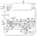
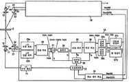
도 1은 본 발명의 제1 실시예의 구성을 도시하고 있다. 실시예에 있어서, 물체(3)의 두께를 측정하기 위해 비임이 일렬로 그리고 서로 반대 방향으로 형성되도록 변위 센서(1A 및 1B)이 배치된다. 변위 센서(1A 및 1B)동일한 구성을 갖고 있다. 우선, 변위 센서(1A 및 1B)이 기술될 것이다.1 shows a configuration of a first embodiment of the present invention. In the embodiment,
물체(3)에 인가되는 비임 광은 종래의 구성에서와 같이 레이져 다이오드(11)로부터 방사되는 적외선 광을 광 투과 렌즈(12)를 통해 통과시킴으로써 제공된다. 레이져 다이오드(11)는 오실레이터(13)의 출력을 LD 구동 회로(14)를 통해 통과시킴으로써 제공되는 주파수 fA를 갖는 구동 신호에 의해 구동된다. 이는 광 출력이 사인파와 같이 변하도록 변조된 레이져 광이 종래의 구성에서와 같이 출력됨을 의미한다.The beam light applied to the
반면, 비임 광을 사용하여 물체(3)을 조사함으로써 물체(3)의 표면 상에 형성되는 광 투과 스폿의 영상은 광 수신 렌즈(22)를 통해 PSD로 구성된 위치 검출 소자(21)의 광 수신면 상에 형성되고, 두 개의 위치 신호(11A 및 12A)는 위치 검출 소자(21)의 광 수신 면 상에 형성된 광 수신 스폿의 위치에 따라 위치 검출 소자(21)로부터 출력된다. 양 위치 신호(11A 및 12A)의 출력값 사이의 비는 광 수신 스폿의 위치에 따라 결정되므로, 물체(3)의 기준 위치로부터의 변위는 위치 신호(11A 및 12A)의 신호값에 기초하여 알아낼 수 있다. 여기서, 기준 위치는 광 수신 스폿이 위치 검출 소자(21)의 광 수신면의 유효 길이의 중심에서 형성될 때 비임 광의 연상 선상에서의 위치이고 기준 위치로부터의 물체(3)의 거리의 변화가 변위로서 구해진다. 그러나, 광 투과 렌즈(12)의 중심 위치는 기준 위치로서 미리 설정되고 및 물체(3)까지의 거리를 알 수 있다.On the other hand, the image of the light transmitting spot formed on the surface of the
본 실시예에 있어서, 스위치 회로(31 및 32)가 시 분할 방식으로 두 개의 채널을 상의 신호를 처리하기 위해 (종래의 두 개의 채널을 요구하는) 회로의 전후에 제공되고, 이에 의해 신호는 1-채널 회로(circuitry)에 의해 처리될 수 있다. 즉, 위치 검출 소자(21)로부터 출력되는 위치 신호(11A 및 12A)는 택일적으로 스위치 회로(31)을 통해 I/V 변환 회로(23)으로 입력된다. 사실상, 위치 신호(11A 및 12A)는 교란 광 등에 의해 생성된 DC 성분을 포함하는 사인파 신호 (즉, DC 성분 때문에 중심이 천이된 사인파 신호)이다. 그러나, 이하의 설명에서, DC 성분은 무시된다. 광 수신 스폿의 위치는 사인파 신호 사이의 진폭비에 대응한다. 위치 신호(11A 및 12A) 중 어느 것이 I/V 변환 회로(23)으로 입력될 것인지는 타이밍 회로(28)로부터 출력되는 스위치 신호(t1)의 제어 하에 결정된다. 도 2(f)와 도 2(i) 사이의 비교로부터 알 수 있는 바와 같이, 스위치 신호(t1)의 지속 기간은 후에 기술될 타이밍 신호(t2)의 지속 기간의 두배로 설정된다.In the present embodiment, the
I/V 변환 회로(23)의 출력은 증폭기(24)로 입력되고, 증폭기(24)는 이 출력을 적당한 증폭 인자로 증폭시킨다. 증폭기(24)의 출력 신호(Va1A, Va2A)는 스위치 회로(31)의 스위치 타이밍에서 위치 신호(11A 및 12A)를 연결하는 신호와 동등하다. 출력 신호(Va1A, Va2A)는 레이져 다이오드(11)로부터 방사되는 비임 광의 매 반 변조 사이클마다 입력 신호를 변환하는 검출 회로(25)에 의해 동기식으로 검출되고, 이에 의해 신호 성분(Vb1A, Vb2A)이 추출된다.The output of the I /
검출 회로(25)는 타이밍 회로(28) (도 2(f) 참조)로부터의 타이밍 신호(t2)에 동기를 맞추어 입력 신호를 검출한다. 타이밍 신호(t2)가 하이 상태라면, 검출 회로(25)는 증폭기(24)의 출력 신호(Va1A, Va2A)를 그대로 취한다. 타이밍 신호(t2)가 로우 상태라면, 검출 회로(25)는 증폭기(24)의 출력 신호(Va1A, Va2A)의 극성을 변환하고 그 결과 신호를 취한다. 신호 성분(Vb1A, Vb2A)는 스위치 회로(31)과 동기가 맞추어지도록 스위치 신호(t1)에 의해 제어되는 스위치 회로(32)에 의해 위치 신호(11A 및 12A)에 대응하는 진동 파형과 같은 한쌍의 신호 성분(Vd1A, Vd2A)으로 분리된다.The
스위치 회로(32)에 의해 제공되는 신호 성분(Vd1A 및 Vd2A)는 로우-패스 필터(26a 및 27b)로 입력되고 DC 성분이 취해진다. 로우-패스 필터(26a 및 27b)에 의해 출력되는 위치 정보 신호(11A 및 12A)는 차 연산부(27a)로 입력되고, 이는 위치 신호(11A 및 12A)의 신호값 사이의 차와 동등한 신호를 제공한다. 위치 정보 신호(V1A 및 V2A)는 또한 합 연산부(27b)으로 입력되고, 이는 위치 신호(11A 및 12A)의 신호값의 합과 동등한 신호를 제공한다. 차 연산부(27a) 및 합 연산부(27b)에 의해 출력되는 위치 정보 신호는 나눗셈 부분(27c)로 입력되고, 이는 차 연산부(27a)의 출력값을 합 연산부(27b)의 출력값으로 나누고 그 결과를 물체까지의 거리와 동등한 신호로서 외부 시스템에 출력한다.The signal components Vd1A and Vd2A provided by the
본 구성에 있어서, 위치 검출 소자(21)로부터 출력되는 위치 신호는 비임 광 변조 사이클과 동기를 맞추어 시 분할 방식으로 택일적으로 처리되고 I/V 변환 회로(23), 증폭기(24), 및 검출 회로(25)는 공유된다. 그리하여, 2-채널 회로가 사용될 때 성분의 온도 특성 변동 또는 상수 변동에 의해 야기되는 오차는 발생되지 않고 더욱이 두 개의 위치 신호(11A 및 12A)는 동기식으로 단일 검출 회로(25)에 의해 검출되므로 오프셋 오차도 생기지 않는다. 더욱이, 검출 회로(25)에 선행하는 단계에서 발생하는 오프셋 오차는 검출 회로(25)를 통해 통과되고, 이에 의해 그 오차는 상쇄될 수 있다. 검출 회로(25)에서 발생하는 근소한 오프셋 오차는 1-채널 회로에 기인하여 비교적 단순한 구성을 갖는 보정 회로에 의해 제거될 수 있다. 더욱이, 두 개의 위치 신호(11A 및 12A)가 동일한 회로에 의해 처리되므로, 레이져 다이오드(11)을 구동하는 신호의 변조 주파수에 변동이 생기더라도 주파수 특성의 차이는 신호가 스위치 회로(32)에 의해 분리될 때까지 생성되지 않고, 거리 측정 결과에 전이 오차(transient error)가 생기지 않는다.In this configuration, the position signal output from the
한편, 본 발명은 변위 센서(1A, 1B)에 변조 제어 회로(34)가 제공되는 것을 특징으로 한다. 변조 제어 입력(VmcINA)를 수신할 때 (실시예에서, VmcINA가 하이 상태일 때), 변조 제어 회로(34)는 오실레이터(13)의 동작을 중단한다. 만일 변조 제어 입력(VmcINA)가 존재하지 않으면, 변조 제어 회로(34)는 오실레이터(13)을 동작시키고 변조 제어 출력(VmcOUTA)을 출력한다 (실시예에서, VmcOUTA를 하이 상태로 설정함). 만일 오실레이터(13)의 동작이 중지되면, 검출 회로(25)도 또한 동작을 중단한다.On the other hand, the present invention is characterized in that the
지금까지 기술한 것은 변위 센서(1A)에 적용된다. 변위 센서(1B)는 동일한 구성이고 변위 센서(1A 및 1B)의 변조 제어 회로(34)는 서로 연결되어 하나의 변위 센서의 변조 제어 출력(VmcOUT)은 다른 변위 센서의 변조 제어 입력(VmcIN)이 된다. 그러므로, 하나의 변위 센서(1A 또는 1B)이 동작하는 동안, 다른 변위 센서(1A 또는 1B)은 비임 광을 생성하지도 검출하지도 않고, 양 변위 센서(1A 및 1B)는 시 분할 방식으로 서로 독립적으로 동작한다. 이는 두 개의 변위 센서(1A 및 1B)가 서로 간섭하지 않는다는 것을 의미한다.What has been described so far is applied to the
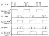
구성의 동작 타이밍이 이하에서 도 2를 참조하여 기술될 것이다. 도 2(a)는 변위 센서(1A)의 오실레이터(13)의 출력(VmA)이고; 도 2(b)는 변위 센서(1A)의 변조 제어 출력(VmcOUTA), 즉 변위 센서(1B)의 변조 제어 입력(VmcINB)이고; 도 2(c)는 변위 센서(1B)의 오실레이터(13)의 출력(VmB)이고; 도 2(d)는 변위 센서(1B)의 변조 제어 출력(VmcOUTB), 즉 변위 센서(1A)의 변조 제어 입력(VmcINA)이다. 이런 관계로부터 알 수 있는 바와 같이, 변위 센서(1A 또는 1B)의 오실레이터(13)이 레이져 다이오드(11)이 광을 방사하도록 동작하는 동안, 다른 변위 센서(1B또는1A)에서는 광 방사가 중단되어, 비임 광 간섭을 억제하기 위해 양 변위 센서(1A 및 1B)의 레이져 다이오드(11)가 동시에 광을 방사하는 것을 방지한다.The operation timing of the configuration will be described below with reference to FIG. 2 (a) is the output VmA of the
위치 검출 소자(21)은 양 변위 센서(1A 및 12B)로부터 광을 수신한다. 그리하여, 변위 센서(1A)에 있어서, 출력 신호(Va1A 및 Va2A)는 오실레이터(13)의 동작이 중지되어 있는 동안아라도 도 2(e)에 도시된 바와 같이 증폭기(24)로부터 제공된다. 그러나, 도 2(f) 및 도 2(g)에 도시된 바와 같이 변위 센서(1A)의 오실레이터(13)이 중지하고 있는 동안, 검출 회로(25)의 동작도 또한 중지되고 (도 2(g)의 신호가 하이 상태일 때 동작은 중단됨), 이에 의해 다른 변위 센서(1A 또는 1B)의 광에 의해 거리가 구해지는 것을 방지한다. 즉, 변위 센서(1A)의 검출 회로(25)의 출력은 도 2(h)에 도시된 바와 같이 되고 변위 센서(1B)의 동작 중에 0 V가 되어 다른 변위 센서(1B)의 동작의 효과는 제거될 수 있다. 도 2(i)는 스위치 회로(32)를 전환하기 위한 타이밍 신호를 도시한다. 신호 성분(Vd1A 및 Vd2A)는 도 2(j) 및 도 2(k)에 도시된 바와 같이 스위치 회로(32)에 의해 분리된다. 분리 후의 처리는 종래의 예의 경우와 비슷하다.The
논의한 바와 같이, 두 개의 변위 센서(1A 및 1B)는 택일적으로 동작하고, 이에 의해 그들은 서로 간섭하지 않고 거리를 측정할 수 있다. 실시예에 있어서, 거리 측정을 실행하기 위해 변위 센서(1A 및 1B)는 레이져 다이오드(11)의 두 개의 광 방사 사이클마다 전환되지만, 사이클은 제한되지 않는다.As discussed, the two
종래의 구성에 있어서, 두 개의 I/V 전환 회로(23a 및 23b), 두 개의 증폭기(24a 및 24b), 및 두 개의 검출 회로(25a 및 25b)가 위치 검출 소자(21)로부터 출력되는 위치 신호(11A 및 12A)에 제공되고; 실시예에서는, I/V 변환 회로(23), 증폭기(24), 및 검출 회로(25)가 단지 하나의 채널로서 제공되고 신호들은 스위치 회로(31 및 32)에 의해 전환된다. 변위 센서(1A 및 1B)는 실시예에서와 같이 구성되고, 이에 의해 위치 신호(11A 및 12A)는 또한 각 변위 센서(1A, 1B)의 오실레이터(13)의 출력이 중지되거나 시작되는 전이 주기에서 동일한 특성으로 처리되어, 거리 측정에서 오차가 발생되지 않는다. 현재의 기술 상태에서, 종래의 구성의 응답성(responsivity)으로 양 위치 신호(11A 및 12A)을 처리하기 위한 회로를 완성하는 것은 어렵다.In the conventional configuration, two I /
완벽한 조절 및 보정이 행해지더라도, 회로는 온도 변화 또는 시간 변화에 기인하여 응답성이 달라질 것이다. 만일 종래의 구성이 채택된다면, 측정 오차는 피할 수 없을 것이다. 반대로, 만일 본 실시예의 구성이 채택된다면, 이러한 종류의 측정 오차는 원리상 일어나지 않고, 측정 정확도가 향상된다.Even if perfect adjustments and corrections are made, the circuit will vary in response due to temperature changes or time changes. If the conventional configuration is adopted, the measurement error will be unavoidable. In contrast, if the configuration of this embodiment is adopted, this kind of measurement error does not occur in principle, and the measurement accuracy is improved.
제2 실시예Second embodiment
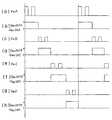
본 발명의 제2 실시예에 있어서, 스위치 회로(31 및 32)는 도 3에 도시된 바와 같이 상이한 스위치 타이밍 신호(t1 및 t5)를 사용하여 제어된다. 도 2와 도 4의 비교로부터 알 수 있는 바와 같이, 검출 회로(25)에 주어지는 타이밍 신호(t2 및 t4)는 또한 제1 실시예의 타이밍 신호와 상이하게 만들어 진다.In the second embodiment of the present invention, the
즉, 제1 실시예의 구성에 있어서, 측정은 변위 센서(1A, 1B)의 동작이 변조 제어 회로(34)에 의해 전환된 바로 직후에 시작된다. 그리하여, 신호 처리가 지연될 수 있고 파형 왜곡이 변위 센서(1A, 1B)의 응답에 따라 발생할 수 있다. 결과적으로, 거리 측정 정확도에 오차가 생길 수 있다. 따라서, 본 실시예에 있어서, 거리 측정은 변위 센서(1A, 1B)가 전환된 후 비임 광 및 처리 회로의 동작이 안정화될 때까지 실행되지 않는다.That is, in the configuration of the first embodiment, the measurement starts immediately after the operation of the
도 4는 변위 센서(1A, 1B)의 동작이 오실레이터(13)의 출력(VmA, VmB)의 한 사이클에서 안정화되는 예를 도시하고 있다. 즉, 도 4(f)에 도시된 바와 같이, 변위 센서(1A, 1B)가 전환된 바로 직후, 파형은 점선에 의해 표시된 바와 같은 파형이 되야 하지만, 실선에 의해 표시된 바와 같은 파형이 된다. 이어서, 도 4(a)에 도시된 바와 같이 전환 바로 직후 비임 광 방사가 시작되고 도 4(h)에 도시된 바와 같이 타이밍 신호(t2)가 검출 회로(25)에 주어지지만, 검출 회로(25)의 출력은 도 4(h)에 도시된 바와 같이 억제된다. 동작과 관련하여, 스위치 회로(31 및 32)의 전환을 위해 사용되는 스위치 신호(t1 및 t5)은 각각 도 4(e) 및 도 4(j)에 도시된 바와 같이 되고, 검출 회로(25)의 출력은 도 4(i)에 도시된 바와 같이 되며, 스위치 회로(32)의 출력은 도 4(k) 및 도 4(l)에 도시된 바와 같이 된다. 간략하게, 제2 실시예는 단지 검출 회로(25)의 출력이 변위 센서(1A, 1B)가 전환된 후 동작이 안정화될 때까지 취해지지 않고 스위치 회로(31 및 32)의 스위치 타이밍이 또한 그에 따라 변한다는 점에서 제1 실시예와 다르다.4 shows an example in which the operation of the
본 구성은 동작이 안정화된 후 거리 측정을 가능하게 하고, 측정 정확도는 더욱 향상된다.This configuration enables distance measurement after the operation is stabilized, and the measurement accuracy is further improved.
제3 실시예Third embodiment
제3 실시예에 있어서, 제1 실시예의 회로 구성에서의 타이밍 신호(t2)는 도 5에 도시된 바와 같이 변화된다. 즉, 제1 실시예에 있어서, 레이져 다이오드(11)은 변위 센서(1A, 1B)의 동작이 변하는 각 시간마다 두 번씩 광을 방사하도록 되어 있고, 제3 실시예에 있어서는, 레이져 다이오드(11)은 변위 센서(1A, 1B)의 동작이 변하는 각 시간마다 여섯 번씩 광을 방사하도록 되어 있다. 광 방사 횟수는 여섯 번으로 한정되어 있는 것은 아니다. 그 횟수는 변위 센서(1A, 1B)의 동작이 변경된 바로 직후의 측정값이 한번 이상의 광 방사에 의해 구해진 측정값의 평균값에 대해 무시될 수 있는 정도로 선택된다. 만일 한번 이상의 광 방사에 의해 구해진 거리가 평균값과 동등한 값을 구하기 위해 결합되면, 오차율이 감소될 수 있다.In the third embodiment, the timing signal t2 in the circuit configuration of the first embodiment is changed as shown in FIG. That is, in the first embodiment, the
제1 실시예와 같이, 제3 실시예는 변위 센서(1A, 1B)가 변경된 바로 직후의 측정값의 오차의 발생에 대한 대책을 제공한다. 그러나, 제2 실시예에서와 같이 동작이 불안정한 동안 구한 측정값을 버릴 필요성은 제3 실시예에서 제거되므로, 제3 실시예에서의 타이밍은 제2 실시예에서의 타이밍보다 간단하다. 제1 실시예에서, 광은 변위 센서(1A, 1B)의 동작이 변하는 각 시간마다 두 번씩 방사되고, 제3실시예에서, 광은 변위 센서(1A, 1B)의 동작이 변하는 각 시간마다 2N번씩 (여기서 N은 2 또는 그 이상임) 방사된다. 제3 실시예의 다른 부품 및 동작은 제1 실시예의 경우와 유사하다.Like the first embodiment, the third embodiment provides a countermeasure against the occurrence of an error in the measured value immediately after the
제4 실시예Fourth embodiment
본 발명의 제4 실시예는 제1 실시예에서의 스위치 회로(31)이 위치 검출 소자(21)로부터 출력되는 위치 신호(11A 및 12A) 중 하나를 항상 I/V 변환 회로(23)으로 입력하는 반면 제4 실시예는 도 6에 도시된 바와 같이 위치 신호(11A 및 12A) 중 어느 것도 I/V 변환 회로(23)으로 입력하지 않는 모드를 갖는 스위치 회로(31)을 사용한다는 점에서 제1 실시예와는 다르다. 간략하게, 제1 실시예에서는, 검출 회로(25)의 출력은 연관 변위 센서(1A, 1B)이 동작하는 동안 중지되지만, 제4 실시예에서는, 위치 검출 소자(21)로부터 I/V 변환 회로(23)로의 입력은 연관 변위 센서(1A, 1B)가 동작하는 동안 억제된다. 이는 도 7에 도시된 바와 같이 세 개의 위치를 취하는 스위치 회로(31)이 스위치 신호(t1) 뿐만 아니라 타이밍 신호(t4)도 사용하여 제어된다는 것을 의미한다.In the fourth embodiment of the present invention, the
제4 실시예의 구성에 따르면, 위치 검출 소자(21)이 통상적으로 수신되는 광량보다 훨씬 더 큰 광량을 갖는 교란광을 수신하더라도, 광이 I/V 변환 회로(23)에 입사되는 것은 방지될 수 있다. 만일 위치 검출 소자(21)의 출력이 비정상적으로 크면, I/V 변환 회로(23) 및 증폭기(24)는 포화되거나 또는 선형 영역에서 사용될 수 없게 된다. 그 결과로, 검출 회로(25)의 출력에서 파형 왜곡이 발생한다. 그러나, 제4 실시예에서 교란광에 기초하여 생성된 위치 신호(11A 및 11B)는 다른 변위 센서(1A, 1B)가 동작하는 동안에 I/V 변환 회로로 입력되지 아니하고, 따라서 상술한 바와 같은 상황을 피할 수 있는 가능성이 높아진다. 제4 실시예의 구성은 특히 다른 변위 센서(1A, 1B)의 광 출력이 큰 경우에 유효하다. 제4 실시예의 다른 부품 및 동작은 제1 실시예의 경우와 유사하다.According to the configuration of the fourth embodiment, even if the
제5 실시예Fifth Embodiment
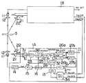
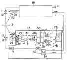
도 8은 본 발명의 제5 실시예의 구성을 도시하고 있다. 변위 센서(1A 및 1B)은 본 발명자에 의해 이전에 행해진 일본 특허 출원 번호 헤이 8-157680의 도 1에 도시된 바와 같이 동작한다. 우선, 변위 센서(1A)의 동작이 논의될 것이다. 위치 검출 소자(21)에 의해 출력된 전기 신호의 위치 신호(11A 및 12A)는 I/V 변환 회로(23a 및 23b)에 의해 전기 신호(Va1A 및 Va2A)로 변환되고 전기 신호(Va1A 및 Va2A)는 동작 회로(29)로 입력되며, 이는 Va1A-Va2A 및 Va1A+Va2A의 연산을 실행하여 그 결과를 스위치 회로(31)로 출력한다. Va1A-Va2A 및 Va1A+Va2A는 택일적으로 스위치 회로(31)을 통해 증폭기(24)로 입력되고, 이는 이어서 그 입력을 적당한 증폭 인자로 증폭한다. Va1A-Va2A 및 Va1A+Va2A중 어느 것이 증폭기(24)로 입력될 것인가는 타이밍 회로(28)로부터 출력되는 스위치 신호(t1)의 제어 하에 결정된다. 도 9(f) 및 도 9(i) 사이의 비교로부터 알 수 있는 바와 같이, 스위치 신호(t1)의 온 지속 기간(on duration)은 이하에서 기술될 타이밍 신호(t2)의 지속 기간의 두배로 설정된다.8 shows the configuration of the fifth embodiment of the present invention. The
증폭기(24)의 출력 신호는 검출 회로(25)에 의해 동기식으로 검출되고 신호 성분(Va1A-Va2A), (Va1A+Va2A)가 추출된다.The output signal of the
검출 회로(25)는 타이밍 회로(28)로부터의 타이밍 신호(t2)에 동기를 맞추어 입력 신호를 검출한다 (도 9(f) 참조). 타이밍 신호(t2)가 하이 상태에 있을 때, 검출 회로(25)는 증폭기(24)의 출력 신호를 그대로 취한다. 타이밍 신호(t2)가 로우 상태일 때, 검출 회로(25)는 증폭기(24)의 출력 신호의 극성을 변환시키고 그 결과 신호를 취한다. 신호 성분(Vd1A-Vd2A), (Vd1A+Vd2A)는 스위치 회로(31)과 동기를 맞추기 위해서 스위치 신호(t1)에 의해 제어되는 스위치 회로(32)에 의해Va1A-Va2A 및 Va1A+Va1A에 대응하는 진동 파형과 갗은 한쌍의 신호 성분Vd1A-Vd2A 및 Vd1A+Vd2A 으로 분리된다.The
스위치 회로(32)에 의해 제공되는 신호 성분(Va1A-Va2A 및 Va1A+Va2A 및 )는 로우-패스 필터(26a 및 26b)으로 입력되고 DC 성분이 취해진다. 신호(V1A-V2A 및 V1A+V2A)는 로우-패스 필터(26a 및 26b)을 통해 출력된다. V1A-V2A는 위치 신호(11A 및 12A) 신호값 사이의 차와 동등한 신호이고 V1A+V2A 는 위치 신호(11A 및 12A)의 신호값의 합과 동등한 신호이다. 로우-패스 필터(26a 및 26b)를 통해 출력되는 신호(V1A-22A 및 V1A+V2A)는 나눗셈 부분(27c)로 입력되고, 이는 이어서(V1A-V2A) / (V1A+V2A)의 연산을 실행하고 그 결과를 물체까지의 거리와 동등한 신호로서 외부 시스템에 출력한다.The signal components Va1A-Va2A and Va1A + Va2A and provided by the
변위 센서(1A)는 스위 회로(31)에 선행하는 단계에서 제공되는 동작 회로(29)에 의해 위치 검출 소자(21)로부터 출력되는 위치 신호(11A 및 12A)에 대응하는 전기 신호(Va1A 및 Va2A)의 감산을 실행한다. 그리하여, 만일 위치 검출 소자(21)로부터 출력되는 위치 신호(11A, 12A)가 동상 잡음(in-phose noise)을 포함한다면, 그 동상 잡음은 동작 회로(29)에 의해 제거될 수 있고, 거리 측정 오차는 종래의 시스템과 비교하여 감소될 수 있으며 동상 잡음의 효과에 의해 야기되는 해상도의 열화가 방지될 수 있다.The
한편, 제5 실시예에 있어서도, 변조 제어 입력(VmcINA)를 수신할 때 (실시예에서, VmcINA가 하이 상태일 때), 변조 제어 회로(34)는 오실레이터(13)의 동작을 중단한다. 만일 변조 제어 입력(VmcINA)가 존재하지 않으면, 변조 제어 회로(34)는 오실레이터(13)을 동작시키고 변조 제어 출력(VmcOUTA)을 출력한다 (실시예에서, VmcOUTA를 하이 상태로 설정). 만일 오실레이터(13)의 동작이 중지되면, 검출 회로(25)도 또한 동작을 중단한다.On the other hand, also in the fifth embodiment, when receiving the modulation control input VmcINA (in the embodiment, when VmcINA is high), the
지금까지 기술한 것은 변위 센서(1A)에 적용된다. 변위 센서(1B)는 동일한 구성이고 변위 센서(1A 및 1B)의 변조 제어 회로(34)는 서로 연결되어 하나의 변위 센서의 변조 제어 출력(VmcOUT)은 다른 변위 센서의 변조 제어 입력(VmcINB)이 된다. 그러므로, 하나의 변위 센서(1A 또는 1B)이 동작하는 동안, 다른 변위 센서(1B 또는 1A)은 비임 광을 생성하지도 검출하지도 않고, 양 변위 센서(1A 및 1B)는 시 분할 방식으로 서로 독립적으로 동작한다. 이는 두 개의 변위 센서(1A 및 1B)가 서로 간섭하지 않는다는 것을 의미한다.What has been described so far is applied to the
본 구성의 동작 타이밍이 이하에서 도 9를 참조하여 기술될 것이다. 도 9(a)는 변위 센서(1A)의 오실레이터(13)의 출력(VmA)이고; 도 9(b)는 변위 센서(1A)의 변조 제어 출력(VmcOUTA), 즉 변위 센서(1B)의 변조 제어 입력(VmcINB)이고; 도 9(c)는 변위 센서(1B)의 오실레이터(13)의 출력(VmB)이고; 도 9(d)는 변위 센서(1B)의 변조 제어 출력(VmcOUTB), 즉 변위 센서(1A)의 변조 제어 입력(VmcINA)이다. 이런 관계로부터 알 수 있는 바와 같이, 하나의 변위 센서(1A 또는 1B)의 오실레이터(13)이 레이져 다이오드(11)이 광을 방사하도록 동작하는 동안, 다른 변위 센서(1B 또는 1A)에서는 광 방사가 중단되어, 비임 광 간섭을 억제하기 위해 양 변위 센서(1A 및 1B)의 레이져 다이오드(11)가 동시에 광을 방사하는 것을 방지한다.The operation timing of this configuration will be described below with reference to FIG. 9 (a) is the output (VmA) of the
위치 검출 소자(21)은 양 변위 센서(1A 및 1B)로부터 광을 수신한다. 그리하여, 변위 센서(1A)에 있어서, 출력 신호(Va1A-Va2A 및 Va1A+Va2A)는 오실레이터(13)의 동작이 중지되어 있는 동안이라도 도 9(e)에 도시된 바와 같이 스위치 회로(31)로부터 제공된다. 그러나, 도 9(f) 및 도 9(g)에 도시된 바와 같이 변위 센서(1A)의 오실레이터(13)이 중지하고 있는 동안, 검출 회로(25)의 동작도 또한 중지되고 (도 9(g)의 신호가 하이 상태일 때 동작은 중단됨), 이에 의해 다른 변위 센서(1A 또는 1B)의 광에 의해 거리가 발견되는 것을 방지한다. 즉, 변위 센서(1A)의 검출 회로(25)의 출력은 도 9(h)에 도시된 바와 같이 되고 변위 센서(1B)의 동작 중에 0 V가 되어 다른 변위 센서(1B)의 동작의 효과는 제거될 수 있다. 도 9(i)는 스위치 회로(32)를 전환하기 위한 타이밍 신호를 도시한다. 신호 성분(Vd1A-Vd2A 및 Vd1A+Vd2A)는 도 9(j) 및 도 9(k)에 도시된 바와 같이 스위치 회로(32)에 의해 분리된다.The
논의한 바와 같이, 두 개의 변위 센서(1A 및 1B)는 택일적으로 동작하고, 이에 의해 그들은 서로 간섭하지 않고 거리를 측정할 수 있다. 실시예에 있어서, 거리 측정을 실행하기 위한 변위 센서(1A 및 1B)는 레이져 다이오드(11)의 두 개의 광 방사 사이클마다 전환되지만, 사이클은 제한되지 않는다.As discussed, the two
종래의 구성에 있어서, 두 개의 I/V 젼환 회로(23a 및 23b), 두 개의 증폭기(24a 및 24b), 및 두 개의 검출 회로(25a 및 25b)가 위치 검출 소자(21)로부터 출력되는 위치 신호(11A 및 12A)에 제공되고; 실시예에서는, 증폭기(24), 검출 회로(25)가 단지 하나의 채널로서 제공되고 신호들은 스위치 회로(31 및 32)에 의해 전환된다. 변위 센서(1A 및 1B)는 실시예에서와 같이 구성되고, 이에 의해 위치 신호(11A 및 12A)는 또한 각 변위 센서(1A, 1B)의 오실레이터(13)의 출력이 중지되거나 시작되는 전이 주기에서 동일한 특성으로 처리되어, 거리 측정에서 오차가 생성되지 않는다. 현재의 기술 상태에서, 종래의 구성의 응답성으로 양 위치 신호(11A 및 12A)을 처리하기 위한 회로를 완성하는 것은 어렵다. 완벽한 조절 및 보정이 행해지더라도, 회로는 온도 변화 또는 시간 변화 때문에 응답성이 달라질 것이다. 만일 종래의 구성이 채택된다면, 측정 오차는 피할 수 없을 것이다. 반대로, 만일 본 실시예의 구성이 채택된다면, 이러한 종류의 측정 오차는 원리상 일어나지 않고, 측정 정확도가 향상된다..In the conventional configuration, two I /
제6 실시예Sixth embodiment
본 발명의 제6 실시예에 있어서, 스위치(31 및 32)는 도 10에 도시된 바와 같이 서로 다른 스위치 타이밍 신호(t1 및 t5)를 사용하여 제어된다. 도 9 및 도 11 사이의 비교로부터 알 수 있는 바와 같이, 검출 회로(25)로 주어진 타이밍 신호(t2 및 t4)는 또한 제5 실시예에서의 타이밍 신호와 다르게 만들어 진다.In the sixth embodiment of the present invention, the
즉, 제1 실시예에서와 같이 제5 실시예의 구성에 있어서, 측정은 변위 센서(1A, 1B)의 동작이 변조 제어 회로(34)에 의해 전환된 바로 직후에 시작된다. 그리하여, 신호 처리는 지연될 수 있고 파형 왜곡은 변위 센서(1A, 1B)의 응답성에 따라 발생할 수 있다. 이어서, 제6 실시예에 있어서, 거리 측정은 제5 실시예에서와 같이 변위 센서(1A, 1B)가 전환된 후 비임 광 및 처리 회로 동작이 안정화될 때까지 실행되지 않는다.That is, in the configuration of the fifth embodiment as in the first embodiment, the measurement starts immediately after the operation of the
도 11은 변위 센서(1A, 1B)의 동작이 오실레이터(13)의 출력(VmA, VmB)의 하나의 사이클 내에서 안정화되는 예를 도시하고 있다. 즉, 변위 센서(1A, 1B)가 전환된 직후, 파형은 점선에 의해 표시된 바와 같은 파형이 될 것이지만 이어서 도 11(f)에 도시된 바와 같이 실선에 의해 표시되는 파형이 될 것이다. 이어서, 도 11(a)에 도시된 바와 같은 스위칭 직후 그리고 도 11(h)에 도시된 바와 같이 검출 회로(25)에 타이밍 신호(t2)가 주어진 직후 비임 광 방사가 시작될 것이지만, 검출 회로(25)의 출력은 도 11(h)에 도시된 바와 갈이 억제될 것이다. 동작과 관련하여, 스위치 회로(31 및 32)의 스위칭을 위해 사용되는 스위치 신호(t1 및 t5)는 각각 도 11(e) 및 11(j)에 도시된 바와 같이 될 것이며, 검출 회로(25)의 출력은 도 11(i)에 도시된 바와 같이 될 것이며, 스위치 회로(32)의 출력은 도 11(k) 및 도 11(l)에 도시된 바와 같이 될 것이다. 간략하게, 제6 실시예는 단지 변위 센서(1A, 1B)가 전환되고 따라서 스위치 회로(31 및 32)의 스위치 타이밍이 또한 변환된 직후 동작이 안정화될 때까지 검출 회로(25)의 출력이 취해지지 않는다는 점에서 제5 실시예와 다르다.FIG. 11 shows an example in which the operation of the
본 구성은 동작이 안정화된 이후에 거리 측정을 가능하게 하고, 측정 정확도는 더욱 향상된다.This configuration enables distance measurement after the operation is stabilized, and the measurement accuracy is further improved.
제7 실시예Seventh embodiment
본 발명의 제7 실시예에 있어서, 제5 실시예의 회로 구성에서의 타이밍 신호(t2 및 t4)는 도 12에 도시된 바와 같이 변화된다. 즉, 제5 실시예에 있어서, 레이져 다이오드(11)은 변위 센서(1A, 1B)의 동작이 변할 때마다 두번씩 광을 방사하도록 만들어지고, 제7 실시예에 있어서는, 레이져 다으오드(11)은 변위 센서(1A, 1B)의 동작이 변할 때마다 여섯 번씩 광을 방사하도록 만들어진다. 광 방사의 횟수는 6번으로 제한되는 것은 아니다. 그 횟수는 변위 센서(1A, 1B)의 동작이 변한 직후의 측정값 오차가 광 방사 광에 의해 한번 이상 구해진 측정값의 평균값에 대해 무시될 수 있는 정도로 선택된다. 만일 한번 이상의 방사 광에 의해 구해진 거리가 평균값과 동등한 값을 구하기 위해 적분되면, 오차 비율이 감소될 수 있다.In the seventh embodiment of the present invention, the timing signals t2 and t4 in the circuit configuration of the fifth embodiment are changed as shown in FIG. That is, in the fifth embodiment, the
제6 실시예와 같이, 제7 실시예는 변위 센서(1A, 1B)의 동작이 변한 바로 직후의 측정값에서 오차가 발생하는 것에 대한 대책을 제공한다. 그러나, 제6 실시예에서와 같이 동작이 불안정한 동안 구해진 측정값을 버릴 필요성은 제7 실시예에서는 제거되어, 제7 실시예에서의 타이밍은 제6 실시예에서의 타이밍보다 더 간단하다. 제5 실시예에 있어서, 광은 변위 센서(1A, 1B)의 동작이 변할 때마다 두 번씩 방사되고, 제7 실시예에 있어서, 광은 변위 센서(1A, 1B)의 동작이 변할 때마다 2N번씩 (여기서 N은 2 또는 그 이상의 값임) 방사된다. 제7 실시예의 다른 부품 및 동작은 제5 실시예의 경우와 유사하다.Like the sixth embodiment, the seventh embodiment provides a countermeasure against the occurrence of an error in the measured value immediately after the operation of the
제8 실시예Eighth embodiment
본 발명의 제8 실시예는 제5 실시예에서의 스위치 회로(31)은 항상 동작 회로(29)로부터 증폭기(24)로 출력되는 신호(Va1A-Va2A 및 Va1A+Va2A) 중 하나를 입력하지만 제8 실시예는 도 13에 도시된 바와 같이 신호(Va1A-Va2A 및 Va1A+Va2A) 중 어느 것도 증폭기(24)로 입력하지 않는 모드를 갖는 스위치 회로(31)을 사용한다는 점에서 제5 실시예와 다르다. 간략하게, 제5 실시예에 있어서, 검출 회로(25)의 출력은 연관 변위 센서(1A, 1B)의 동작 중에 중지되고, 제8 실시예에 있어서, 동작 회로(29)로부터 증폭기(24)로의 입력은 연관 변위 센서(1A, 1B)의 동작 중에 억제된다. 이는 세 개의 위치를 취하는 스위치 회로(31)는 도 14에 도시된 바와 같이 스위치 신호(t1)뿐만 아니라 타이밍 신호(t4)를 사용하여 제어된다는 것을 의미한다.In the eighth embodiment of the present invention, the
제8 실시예의 구성에 따르면, 비록 위치 검출 소자(21)이 통상적으로 수신되는 광량보다 극적으로 더 큰 광량을 갖는 교란광을 수신하더라고, 위치 검출 소자의 출력은 증폭기(24)로 입력되는 것이 방지될 수 있다. 만일 위치 검출 소자(21)의 출력이 비정상적으로 크면, 증폭기(24)는 포화되거나 또는 선형 영역에서 사용될 수 없다. 그 결과로, 파형 왜곡이 검출 회로(25)의 출력에서 발생한다. 제8 실시예에 있어서, 그러나, 교란광에 기초하여 생성된 위치 신호(11A 및 11B)에 기초한 동작 회로(29)의 출력은 다른 변위 센서(1A, 1B)의 동작 중에 증폭기(24)로 입력되지 아니하고, 따라서 상술한 바와 같은 상황이 회피될 수 있는 가능성이 일어난다. 그 결과, 측정 결과의 신뢰성은 향상된다. 제8 실시예의 구성은 특히 다른 변위 센서(1A, 1B)의 광출력이 큰 경우에 유효하다. 제8 실시예의 다른 부품 및 동작은 제5 실시예의 경우와 유사하다.According to the configuration of the eighth embodiment, even though the
제9 실시예9th Example
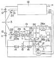
상술한 변위 센서(1A 및 1B)는 다수의 센서가 사용될 때, 서로 간섭을 방지하기 위해 변경되고, 그들은 독자적 사용에 대해서 고려되지 않고 만일 하나의 변위 센서(1A, 1B)가 다른 하나의 변위 센서(1A, 1B)데 연결되어 있을 때에만 사용될 수 있다. 그러므로, 그들은 독자적으로 사용되는 변위 센서와는 별도로 생산되어야 한다. 만일 독자적으로 사용되는 변위 센서 및 서로간의 간섭을 방지하기 위해 변경된 변위 센서(1A, 1B)가 생산되고, 생산 라인이 복잡해지고 재고품 관리가 힘들어진다. 독자적으로 하나의 변위 센서(!A, 1B)를 사용하기 위한 동작 모드를 변경하거나 센서의 목적에 응답하여 상호 간섭을 방지하는 것이 필요하게 될 수 있다. 동작 모드를 변경하기 위해서, 수동형 스위치가 또한 사용될 수 있지만, 비용 감소 및 최소화는 달성하기 어렵고 스위치를 수동으로 다루는 것은 곤란하다. 게다가, 변위 센서(1A, 1B)의 동작 모드를 시 관리 방식으로 사용하는 것은 실질적으로 불가능하다.The
이어서, 본 발명의 제9 실시예는 변위 센서(1A, 1B)를 제공하는데, 이는 상호 간섭을 방지할 뿐만 아니라 동작 모드를 변경하기 위해 수동 스위치를 사용하지 않고도 독자적으로 사용될 수 있다. 즉, 모드 판단 파형 형성 회로(34a)이 도 15에 도시된 바와 같이 동작 모드를 판단하기 위해 변조 제어 회로(34)에 더해진다. 이하에서, 상호 간섭을 방지하기 위한 동작 모드는 "간섭 방지 모드"라고 불리울 것이며 독자적인 사용을 위한 동작 모드는 "단일 모드"라고 불리울 것이다.Subsequently, the ninth embodiment of the present invention provides
도 16에 도시된 바와 같이, 모드 판단 파형 형성 회로(34a)는 두 개의 임계값(Th1 및 Th2)를 갖고 있고 초과, 동일, 또는 미만 관계에 대해여 임계값(Th1, Th2)과 변조 제어 입력(VmcINA, VmcINB) 사이의 비교를 행한다. 임계값(Th2)는 동작 모드를 변경하기 위해 사용된다. 변조 제어 입력(VmcINA, VmcINB)이 임계값(Th2)보다 큰 경우, 간섭 방지 모드가 선택되고, 변조 제어 입력(VmcINA, VmcINB)이 임계값(Th2)보다 작은 경우, 단일 모드가 선택된다. 이는 모드 판단 파형 형성 회로(34a)가 오실레이터(13)으로 모드 신호 모드를 주고, 이에 의해 또 다른 변위 센서(1A, 1B)가 존재할 때 그리고 또 다른 변위 센서(1A, 1B)가 존재하지 않을 때 동작을 변경한다. 임계값(Th1)은 다른 하나의 변위 센서(1A, 1B)가 간섭 방지 모드에서 동작하고 있는지 여부를 판단하기 위해 사용된다.As shown in FIG. 16, the mode decision
그러한 변화를 만들기 위해, 각각의 변위 센서(1A, 1B)에는 정전류원(34b), 정전압원(Va, Vb), 및 저항(R1 및 R2)가 제공된다. 모드 판정 파형 형성 회로(34a)로의 입력이 저항(R1)에 의해 강하되므로, 만일 변조 제어 입력(VmcINA, VmcINB)가 존재하지 않으면, 즉, 다른 변위 센서(1A, 1B)가 연결되어 있지 않으면, 모드 판정 파형 형성 회로(34a)로의 입력은 0 V이고, 그리하여 임계값(Th2)보다 더 낮게 되어 단일 모드가 선택된다.To make such a change, each
반면, 변위 센서(1A, 1B)의 변조 제어 출력(VmcOUTA, VmcOUTB)은 저항(R2)를 통해 임계값(Th2)보다 더 높은 전압을 갖는 정전압원(Va, Vb)에 연결되어 있다. 그리하여, 다른 변위 센서(1A, 1B)가 연결되어 있으면, 모드 판정 파형 형성 회로(34a)가 간섭 방지 모드로 모드 신호 모드를 설정한다. 정전류원(34b)는 다른 하나의 변위 센서(1A, 1B)의 동작 중에 변위 센서(1A, 1B)의 동작을 중지시키기 위해 사용된다. 동작 중인 변위 센서(1A, 1B)는 변조 제어 출력(VmcOUTA, VmcOUTB)을 임계값(Th1)보다 더 높은 전압값으로 올리기 위해 정전류원(34b)로부터 저항(R2)로 전류를 흐르게 한다. 도 15에서 정전류원(34b)의 근처에 도시된 화살표는 정전류원(34b)를 온/오프 제어하기 위해 주어진 신호를 나타낸다. 하나의 변위 센서(1A, 1B)는 도 16(a) 내지 도 16(d)에 도시된 바와 같이 다른 하나가 동작하고 있는 동안 중지한다. 간섭 방지 모드에 있어서, 변위 센서(1A, 1B)가 동작하는지 여부는 임계값(Th1 및 Th2)의 결합에 의해서 결정된다. 그리하여, 모드 판단 파형 형성 회로(34a)는 결합에 따라 도 16(e)에 도시된 바와 같이 제1 실시예 및 제5 실시예에서 변조 제어 입력과 동등한 신호(VmcINA', VmcINB')를 생성하고 신호(VmcINA, VmcINB)에 의해 오실레이터(13)을 제어한다.On the other hand, the modulation control outputs VmcOUTA and VmcOUTB of the
제9 실시예에서, 동작 모드를 변경하기 위한 임계값(Th2)은 다른 하나의 변위 센서(1A, 1B)가 동작하고 있는지 여부를 판단하기 위해 사용되는 임계값(Th1)보다 더 낮게 설정된다. 그러나, 임계값(Th1 및 Th2) 사이의 초과 또는 미만 관계는 또한 반대 관계로 설정될 수 있다. 이 경우에 있어서, 변조 제어 입력(VmcINA, VmcINB)를 상승시키고 정전류원(34b), 정전압원(Va, Vb), 저항(R2) 등 사이의 관계를 변경시키는 것이 필요하다.In the ninth embodiment, the threshold value Th2 for changing the operation mode is set lower than the threshold value Th1 used for determining whether the
물론, 동작 모드를 변경시키는 것은 상술한 실시예에 의해 제한되지 않는다. 예를 들어, 도 15(b) 내지 도 15(d)에 도시된 바와 같이, 동작 모드를 변경시키는 것은 클록 펄스를 생성하는 정전류원 및 모드 판단을 위한 두 개의 정전류원을 포함하는 구조, 클록 펄스를 생성하는 정전력원 및 모드 변경을 위한 두 개의 정전력원을 포함하는 구조, 및 소프트웨어에 의한 클록 펄스 형성 및 모드 판단에 의해 달성된다. 제1 및 제2 구조는 도 16에 도시된 바와 같이 DC 성분이 중첩된 동일한 파형을 사용하고 있다. 제3 방법에 있어서, 모드 판단은 소프트웨어에 의해 행해져 파형은 Gnd가 "로우"에 대응하고 Vcc가 "하이"에 대응하도록 하는 논리 파형에 대응하게 된다.Of course, changing the operation mode is not limited by the above-described embodiment. For example, as shown in Figs. 15 (b) to 15 (d), changing the operation mode includes a structure comprising a constant current source for generating clock pulses and two constant current sources for mode determination, clock pulses. A structure comprising a constant power source for generating a constant power source and two constant power sources for mode change, and clock pulse formation and mode determination by software. As shown in Fig. 16, the first and second structures use the same waveform in which the DC components are superimposed. In the third method, mode determination is performed by software so that the waveform corresponds to a logic waveform such that Gnd corresponds to "low" and Vcc corresponds to "high".
도 15(b)에 도시된 바와 같이, 정전류원이 모드 판단을 위해 사용된다. 정전류원은 클록의 생성을 위해 하나의 정전류원이 직접 전류원을 사용하고 다른 정전류원이 택일적인 전류원을 사용하도록 하는 방식으로 병렬로 연결된다.As shown in Fig. 15B, a constant current source is used for mode determination. Constant current sources are connected in parallel in such a way that one constant current source uses a direct current source and another constant current source uses an alternative current source for the generation of the clock.
도 15(c)에 도시된 바와 같이, 정전력원이 클록 파형 형성을 위해 사용된다. 두 개의 전력원은 클록의 생성을 위해 하나의 정전력원이 직접 전류원을 사용하고 다른 정전력원이 택일적인 전류원을 사용하도록 하는 방식으로 직렬로 연결된다.As shown in Fig. 15C, a constant power source is used for clock waveform formation. The two power sources are connected in series in such a way that one constant power source uses a direct current source and the other constant power source uses an alternative current source for the generation of the clock.
도 15(c)에 도시된 바와 같이, 마이크로프로세서 등에 의해 소프트웨어 처리가 수행된다. 출력 단자는 통상의 클록 파형을 출력하고 입력 단자는 신호가 존재하는지 여부에 상관없이 모드 판단이 수행되도록 소프트웨어로 인터럽트 기능을 사용한다.As shown in Fig. 15C, software processing is performed by a microprocessor or the like. The output terminal outputs a normal clock waveform and the input terminal uses an interrupt function in software to perform mode determination whether or not a signal is present.
제10 실시예Tenth embodiment
본 발명의 제10 실시예는 도 17에 도시된 바와 같이 세 개의 변위 센서(1A, 1B, 및 1C)를 사용한다. 본 실시예에 있어서, 변위 센서(1A, 1B, 및 1C)가 나란히 배치되어 있는 예가 배치례로서 도시되어 있는데, 여기서 그들은 서로 간섭한다. 배치례에 있어서, 측면의 변위 센서(1B 및 1C)가 중앙의 변위 센서(1A)와 간섭할 수 있지만 측면의 변위 센서(1B 및 1C)는 서로 간섭하지 않는다는 가능성이 가정되고 있다.The tenth embodiment of the present invention uses three
그러므로, 변위 센서(1B 및 1C)을 택일적으로 동작시킬 필요는 없지만 변위 센서(1B, 1C)와 변위 센서(1A)를 택일적으로 동작시킬 필요는 있다. 따라서, 도 18에 도시된 바와 같이, 변위 센서(1B 및 1C)의 양 변위 제어 입력(VmcINB 및 VmcINC)는 변위 센서(1A)의 변조 제어 출력(VmcOUTA)이다. 마찬가지로, 변위 센서(1B 및 1C)의 변조 제어 출력(VmcOUTB 및 VmcOUTC)은 변위 센서(1A)의 변조 제어 입력(VmcINA)이다. 여기서, 세 개의 변위 센서(1A, 1B, 및 1C)이 도시되어 있지만, 동일한 것이 더 큰 수의 변위 센서의 설치에 적용될 수 있으며; 변조 제어 입력 및 변조 제어 출력은 서로 간섭하지 않는 변위 센서들 사에에 공통으로 만들어질 수 있고 서로 간섭하는 변위 센서는 서로 변조 제어 입력 및 변조 제어 출력을 줄 수 있다.Therefore, it is not necessary to operate the
한편, 본 실시예에 있어서, 각각의 변위 센서(1A, 1B, 및 1C)의 변조 제어 회로(343)의 출력 (변조 제어 출력(VmcOUTA, VmcOUTB, VmcOUTC))은 전류 출력이고 변조 제어 회로(34)의 입력 (변조 제어 입력(VmcINA, VmcINB, VmcINC))은 풀-다운 저항(R1)이다.On the other hand, in this embodiment, the output (modulation control outputs VmcOUTA, VmcOUTB, VmcOUTC) of the modulation control circuit 343 of each of the
그러므로, 도 19에 도시된 바와 같이, 변위 센서(1A)가 동작하고 있는 동안, 변위 센서(1B, 1C)의 거리 측정 동작은 중지되고, 변위 센서(1B, 1C)가 동작하고 있는 동안 변위 센서(1A)의 거리 측정 동작은 중지된다. 도면에서 변위 센서(1B, 1C)의 동작은 동기식으로 동작하고 있는 것으로 보이나, 타이밍은 그들 사이에서 취해지지 않는다. 변위 센서(1B 및 1C)가 반드시 동시에 거리 측정 동작을 중지할 필요는 없다. 그러나, 변위 센서(1A)의 거리 측정은 어느것이 더 나중인지에 따라 변위 센서(1B 또는 1C)의 거리 측정 동작이 종료된 후에 시작하므로, 변위 센서(1A 및 1B, 1C) 사이의 상호 간섭은 발생하지 않는다.Therefore, as shown in FIG. 19, while the
본 실시예는 다수의 변위 센서가 두 개의 그룹으로 분류되고 서로 연결되어 그들이 서로 간섭하지 않는 구성을 제공하고 있다. 본 실시예에 있어서, 세 개의 변위 센서가 도시되어 있지만, 변위 센서의 수는 각각의 변위 센서의 전류 용량을 제외하고는 제한적인 것이 아니다. 제10 실시예의 다른 부품 및 동작은 제1 및 제5 실시예의 경우와 유사하다.This embodiment provides a configuration in which a plurality of displacement sensors are classified into two groups and connected to each other so that they do not interfere with each other. In the present embodiment, three displacement sensors are shown, but the number of displacement sensors is not limited except for the current capacity of each displacement sensor. Other parts and operations of the tenth embodiment are similar to those of the first and fifth embodiments.
제11 실시예Eleventh embodiment
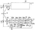
본 발명의 제11 실시예에 있어서, 네 개의 변위 센서(1A, 1B, 1C, 및 1D)가 도 20에 도시된 바와 같이 두 개씩 서로 나란히 배치되어 있고 두 개의 그룹은 서로 반대로 배치되어 있다. 그러한 배치례에 있어서, 네 개의 변위 센서(1A, 1B, 1C, 및 1D)가 서로 간섭할 가능성이 있다. 다수의 변위 센서(1A, 1B, 1C, 및 1D)가 서로 간섭하는 것을 방지하기 위해서, 본 실시예에서는, 각각의 변위 센서(1A, 1B, 1C, 및 1D)는 도 20에 도시된 바와 같이 변조 제어 입력(VmcINA, VmcINB, VmcINC, 및 VmcIND)으로의 입력 신호의 상승 엣지 상에서 거리 측정 동작을 시작하고, 변위 센서(1A, 1B, 1C, 및 1D)의 변조 제어 출력(VmcOUTA, VmcOUTB, VmcOUTC, 및 VmcOUTD)는 서로 다른 변위 센서(1A, 1B, 1C, 및 1D)의 변조 제어 입력(VmcINA, VmcINB, VmcINC, 및 VmcIND)에 순차로 연결되어 있다. 특히, 변위 센서(1A)의 변조 제어 출력(VmcOUTA)은 변위 센서(1B)의 변조 제어 입력(VmcINB)에 연결되어 있고, VmcOUTB는 VmcINC로, VmcOUTC는 VmcIND로, 그리고 VmcOUTD는 VmcINA로 연결되며, 이에 의해 변위 센서(1A, 1B, 1C, 및 1D)는 직렬로 또는 고리와 같이 연결되어 있다.In the eleventh embodiment of the present invention, four
본 구성에 있어서, 거리 측정 동작을 중지한 후에, 하나의 변위 센서(1A, 1B, 1C, 및 1D)은 다른 하나의 변위 센서(1A, 1B, 1C, 및 1D)로부터 주어진 변조 제어 입력(VmcINA, VmcINB, VmcINC, VmcIND)가 상승할 때가지 거리 측정 동작을 중지한다. 그러므로, 정적인 동작에 있어서, 도 21에 도시된 바와 같이, 변위 센서(1A)가 거리 측정을 실행하는 동안, 변위 센서(1B)의 동작은 중지되고, 다른 변위 센서(1C 및 1D)는 변조 제어 입력(VmcINC 및 VmcIND)가 각각 상승할 때까지 거리 측정 동작을 중지한다. 변위 센서(1A)의 거리 측정 동작의 완료시에, 변위 센서(1B)로의 변조 제어 입력(VmcINB)은 상승하고, 그리하여 변위 센서(1B)는 동작을 시작한다. 이어서, 변위 센서(1C 및 1D)는 순차로 동작을 택일적으로 시작하고 변위 센서(1D)의 동작의 완료시에, 변위 센서(1A)로의 변조 제어 입력(VmcINA)는 상승하고 변위 센서(1A)는 다시 동작을 시작한다.In this configuration, after stopping the distance measuring operation, one
논의한 바와 같이, 변위 센서(1A, 1B, 1C, 및 1D)는 거리 측정 동작을 순차로 실행하여, 요구되는 많은 변위 센서는 직렬로 연결될 수 있다. 더욱이, 두 세트가 한번에 변위 센서 사이에 연결되어 있고, 그 연결이 용이하다.As discussed, the
제10 및 제11 실시예의 구성은 공통적으로 만들어질 수 있으며, 두 개의 그룹으로 분류되는 변위 센서 사이의 간섭의 방지 또는 변위 센서 서로간의 간섭의 방지가 단지 변위 센서의 연결 방식의 변경에 의해 간단히 설정될 수 있다.The arrangements of the tenth and eleventh embodiments can be made in common, and the prevention of interference between displacement sensors or the prevention of interference between displacement sensors, which are classified into two groups, is simply set by simply changing the connection method of the displacement sensors. Can be.
제12 실시예12th Example
본 발명의 제12 실시예의 변위 센서(1A 및 1B)는 도 22에 도시된 바와 같이 나눗셈부(27c)없이 거리를 구한다. 합연산부(27b)의 출력 전압은 위치 검출 소자(21)로 입사되는 모든 광량과 동등하고 비교 회로(17)은 출력 전압을 기준 전압(Vref)와 비교하고 합연산부(27b)의 출력 전압과 기준 전압(Vref) 사이의 차와 동등한 신호를 피드백 제어 회로(16)으로 출력한다. 피드백 제어 회로(16)은 변조기(15)를 통해 캐리어로서 타이밍 회로(28)로부터의 타이밍 신호(t2)를 사용하여 진폭 변조를 실행하고 LD 구동 회로(14)를 통해 레이져 다이오드(11)을 구동한다. 간략하게, 레이져 다이오드(11)로부터의 광 출력은 위치 검출 소자(11)에서 수신된 광량에 응답하여 피드백 제어를 받는다.The
만일 본 구성이 채택되면, 합연산부(27b)의 출력은 일정한 값으로 기준 전압(Vref)에서 유지되고 거리 탐색 동작이 수행될 때의 분자는 일정한 값이 되어, 차연산부(27c)의 출력은 물체(3)까지의 거리와 동등하게 된다. 이는 나눗셈부(27c)에 대한 필요성을 제거한다. 더욱이, 레이져 다이오드(11)의 광 출력은 위치 검출 소자(21)에서 수신된 광량에 응답하여 조절될 수 있으므로, 광량은 반사 계수 또는 물체(3)의 거리에 응답하여 조절될 수 있고 거리는 처리 회로의 동적 범위 내에서 정확하게 측정될 수 있다. 제12 실시예의 다른 부품과 동작은 제1 실시예의 경우와 유사하다.If this configuration is adopted, the output of the
제13 실시예Thirteenth embodiment
제12 실시예와 같이, 본 발명의 제13 실시예는 도 23에 도시된 바와 같이 합연산부(27b)의 출력을 일정하게 유지하기 위해 피드백 제어를 실행한다. 이는 증폭기(24) 대신에 가변 증폭 인자를 갖는 가변 증폭기(24')를 사용하고 레이져 다이오드(11)의 광 출력 대신에 가변 증폭기(24')의 증폭 인자를 변경하기 위해 피드백 제어 회로(16)이 사용된다. 합연산부(27b)의 출력은 피드백 제어에 의해 일정한 값으로 유지될 수 있으므로, 차연산부(27a)의 출력은 거리 측정값으로 사용될 수 있다. 제13 실시예의 다른 부품 및 동작은 제1 실시예의 경우와 유사하다.As in the twelfth embodiment, the thirteenth embodiment of the present invention executes feedback control to keep the output of the combining
제14 실시예Fourteenth embodiment
본 발명의 제14 실시예는 도 24에 도시된 바와 같이 제12 실시예 및 제13 실시예의 구성의 결합과 동등하다. 즉, 레이져 다이오드(11)의 광 출력 및 가변 증폭기(24')의 증폭 계수의 피드백 제어는 합연산부(27b)의 출력 전압을 일정하게 유지하기 위해 실행된다. 이 시점에서, 피드백 제어는 다음과 같이 실행된다. 일정한 수신 광량은 기준 (예를 들어, 이 양은 백색 세라믹이 기준 거리 상에 놓여 있도록 판단함)으로서 작용한다. 수신 광량이 기준값보다 크면, 피드백은 광 전력의 감소를 실행하고, 수신 광량이 기준값보다 작으면, 피드백은 증폭 인자의 증가를 실행한다.The fourteenth embodiment of the present invention is equivalent to the combination of the configuration of the twelfth and thirteenth embodiments as shown in FIG. That is, feedback control of the light output of the
즉, 수신 광량이 기준값보다 더 크면, 증폭 인자는 최소값으로 다시 말하여, 일정한 조건으로 설정되어, 최상의 조건의 해상도에서 처리를 실행하고 수신 광량의 증가에 관계된 광 전력을 억제하는 것이 가능하다. 수신 광량이 기준값보다 더 작으면, 광 전력은 최대값, 다시 말하여 일정한 조건으로 설정되어, 최대 수신 광량을 획득하고 수신 광량의 감소와 관계된 증폭 인자를 증가시키는 것이 가능하다.In other words, if the received light amount is larger than the reference value, the amplification factor is set to the minimum value, that is, the constant condition, so that it is possible to execute the processing at the resolution of the best condition and suppress the optical power related to the increase in the received light amount. If the received light amount is smaller than the reference value, the optical power is set at a maximum value, that is, a constant condition, so that it is possible to obtain the maximum received light amount and increase the amplification factor related to the decrease in the received light amount.
상술한 바와 같이, 두 개의 피드백 동작 영역은 서로 중첩되지 않으므로 수신 광량의 동적 범위는 매우 넓게 된다.As described above, the two feedback operation regions do not overlap each other, so that the dynamic range of the received light amount becomes very wide.
다른 말로, 물체(3)의 반사 계수가 측정될 수 있는 범위는 제12 또는 제13 실시예보다 더 넓게 취해질 수 있다. 제14 실시예의 다른 부품 및 동작은 제1 실시예의 경우와 유사하다.In other words, the range in which the reflection coefficient of the
제15 실시예Fifteenth embodiment
본 발명의 제15 실시예는 도 25에 도시된 바와 같은 구성을 제공한다. 제15 실시예는 Va1a-Va2A 및 Va2A가 연산 회로(29)로부터 출력되고, 제5 실시예의 스위치 회로(32)가 필요하지 않고, 연산 회로(30)이 검출 회로(25)의 출력에 기초하여 선정된 동작을 실행하기 위해 제공되고, 나눗셈부(27c)가 연산(V1A-V2A)/(V1A+kXV2A)를 실행하고 여기서 연산 회로(30)은 Vd1A-Vd2 및 Vd2를 출력하고 로우-패스 필터(26a 및 26b)가 각각 V1A-V2A 및 V2A를 출력한다는 점에서 제5 실시예와는 다르다. 가산기(27b')는 V1A+kXV2A를 출력하는데, 여기서 k는 광학적 비선형 특성을 보정하기 위한 상수이다. 그러므로, 제15 실시예에 있어서, 나눗셈부(27c)의 출력은 반사 계수의 총 합계 및 물체(3)의 표면 상에서의 광 수신량에 상관없이 위치 검출 소자(21)에 의해 출력되는 위치 신호(11A, 12A)를 정규화함으로써 물체까지의 거리에 대응하는 신호가 된다. 스위치 회로(32)를 요구하지 않는 본 실시예는 스위치 동작 시간 지연 또는 스위칭 잡음에 의해 야기되는 오차의 발생을 감소시킬 수 있고 스위치 회로(32)가 제공되는 실시예와 비교할 때 거리 측정의 정확도를 향상시킬 수 있다.A fifteenth embodiment of the present invention provides a configuration as shown in FIG. In the fifteenth embodiment, Va1a-Va2A and Va2A are output from the
제15 실시예의 다른 부품 및 동작은 제5 실시예의 경우와 유사하다.Other parts and operations of the fifteenth embodiment are similar to those of the fifth embodiment.
제16 실시예Sixteenth embodiment
본 발명의 제16 실시예는 도 26에 도시된 바와 같은 구성을 제공한다. 제16 실시예는 서로 다른 타이밍 신호(t3)가 검출 회로(25)에 주어지고, 제5 실시예의 스위치 회로(32)가 요구되지 않고, 나눗셈부(27c)가 연산(V1A-V2A)/(V1A+kXV2A)를 실행하고 여기서 로우-패스 필터(26a 및 26b)가 각각 V1A-V2A 및 V2A를 출력한다는 점에서 제5 실시예와는 다르다. 타이밍 신호(t3)는 스위치 신호(t1)과 위상이 90 도 다르다. 제16 실시예의 다른 부품 및 동작은 제5 실시예의 경우와 유사하다.A sixteenth embodiment of the present invention provides a configuration as shown in FIG. In the sixteenth embodiment, different timing signals t3 are given to the
제17 실시예Example 17
본 발명의 제17 실시예는 도 27에 도시된 바와 같은 구성을 제공한다. 제16 실시예는 서로 다른 타이밍 신호(t3)가 검출 회로(25)에 주어지고, 제5 실시예의 스위치 회로(32)가 요구되지 않고, 나눗셈부(27c)가 연산(V1A-V2A)/(V1A+kXV2A)를 실행한다는 점에서 제5 실시예와는 다르다. 제17 실시예의 다른 부품 및 동작은 제5 실시예의 경우와 유사하다.A seventeenth embodiment of the present invention provides a configuration as shown in FIG. In the sixteenth embodiment, different timing signals t3 are given to the
제18 실시예Eighteenth embodiment
한편 제5 실시예의 변위 센서(1A 및 1B)는 각각 나눗셈부(27c)를 포함하고 있다. 본 발명의 제18 실시예의 변위 센서(1A 및 1B)는 도 26에 도시된 바와 같이 나눗셈부(27c) 없이 거리를 구한다. 제18 실시예의 구성은 본 발명자에 의해 전에 행해진 일본 특허 출원 헤이8-157680호의 도 9에 도시된 것과 실질적으로 동일하게 동작한다. (일본 특허 출원 헤이8-157680호에서의 가산기(13)과 동등한) 가산기(27b')의 출력 전압, V1+kXV2는 위치 검출 소자(21) 상에 입사되는 모든 광량과 동등한 것으로 가정되고 비교 회로(17)은 출력 전압을 기준 전압(Vref)와 비교하고 가산기(27b')의 출력 전압과 기준 전압(Vref) 사이의 차와 동등한 신호를 피드백 제어 회로(16)으로 출력한다. 피드백 제어 회로(16)은 변조기(15)를 통해 캐리어로서 타이밍 회로(28)로부터의 타이밍 신호(t2)를 사용하여 진폭 변조를 실행하고 LD 구동 회로(14)를 통해 레이져 다이오드(11)을 구동한다. 간략하게, 레이져 다이오드(11)로부터의 광 출력은 위치 검출 소자(11)에서 수신된 광량에 응답하여 피드백 제어를 받는다. 더욱이, 가변 증폭 인자를 갖는 가변 증폭기(24')가 제5 실시예의 증폭기(24) 대신에 사용되고 가변 증폭기(24')의 증폭 인자는 피드백 제어 회로(16)에 의해 변경된다. 즉, 제18 실시예에 있어서 제14 실시예에서와 같이, 레이져 다이오드(11)의 광 출력 및 가변 증폭기(24')의 증폭 인자의 피드백 제어가 실행된다. 가산기(27b')의 출력 전압으로서 구해진 값, V1+kXV2가 결과로서 생긴다.On the other hand, the
만일 본 구성이 채택되면, 가산기(27b')의 출력은 일정한 값으로 기준 전압(Vref)에서 유지되고 거리 탐색 동작이 수행될 때의 분자는 일정한 값이 되어, 로우-패스 필터(26a)의 출력, V1A-V2A는 물체(3)까지의 거리와 동등하게 된다. 이는 나눗셈부(27c)에 대한 필요성을 제거한다. 더욱이, 레이져 다이오드(11)의 광 출력은 위치 검출 소자(21)에서 수신된 광량에 응답하여 조절될 수 있으므로, 광량은 반사 계수 또는 물체(3)의 거리에 응답하여 조절될 수 있고 거리는 처리 회로의 동적 범위 내에서 정확하게 측정될 수 있다. 제18 실시예의 다른 부품과 동작은 제5 실시예의 경우와 유사하다.If this configuration is adopted, the output of the
본 발명에 따르면, 물체를 광 방사 소자로부터 적합한 사이클로 변조된 비임 광으로 조사하고, 물체의 표면 상에 광 투과 스폿을 형성하고, 위치 검출 소자의 광 수신면 상에 광 투과 스폿의 영상을 형성하고, 이에 의해 광 수신 스폿을 제공하고, 처리 부분에 의해 광 수신 스폿의 위치에 기초하여 물체까지의 거리를 알아내는 광학 변위 측정 장치가 제공되는데, 이 광학 변위 측정 장치는 거리 측정 동작을 수행하기 위해 사이클 내에서 적합한 횟수만큼 비임 광으로 물체를 조사하고 이어서 거리 측정 동작을 중지하고 동작 중지를 나타내는 변조 제어 출력을 생성하며 외부로부터 동작 시작을 나타내는 변조 제어 입력의 수신시에 다시 거리 측정 동작을 시작하기 위한 변조 제어 회로를 포함한다. 예를 들어, 만일 두 개의 광학 변위 측정 장치가 염려되는 위치 관계로 배치되면, 광학 변위 측정 장치는 서로 간섭할 수 있고, 광학 변위 측정 장치 중 하나의 변조 제어 출력은 다른 것의 변조 제어 입력으로서 주어지고, 이에 의해 양 광학 변위 측정 장치가 택일적으로 동작하도록 한다. 그 결과로, 상호 간섭을 방지할 수 있는 잇점이 제공된다. 이는 두 개의 센서가 서로 인접하도록 형성되거나 간섭에 의해 야기되는 해상도 또는 선형성의 열화없이 사용되기 위해 서로 대향되게 배치될 수 있다는 것을 의미한다.According to the invention, the object is irradiated with a suitable cycle-modulated beam of light from the light emitting element, forms a light transmitting spot on the surface of the object, forms an image of the light transmitting spot on the light receiving surface of the position detecting element, Thereby, there is provided an optical displacement measuring device which provides a light receiving spot and finds out the distance to the object based on the position of the light receiving spot by the processing portion, which optical cycle measuring device performs a cycle for performing the distance measuring operation. For irradiating an object with a beam of light within a suitable number of times and then for stopping the ranging operation, generating a modulation control output indicative of an outage and starting the distance measurement operation again upon receipt of a modulation control input indicative of the start of operation from the outside. And a modulation control circuit. For example, if two optical displacement measuring devices are arranged in a positional position of concern, the optical displacement measuring devices may interfere with each other, and the modulation control output of one of the optical displacement measuring devices is given as a modulation control input of the other. This allows the two optical displacement measuring devices to alternatively operate. As a result, an advantage is provided that can prevent mutual interference. This means that the two sensors can be formed adjacent to each other or placed opposite one another for use without degradation in resolution or linearity caused by interference.
본 발명에서와 같이, 광학 변위 측정 장치는 거리 측정 동작을 시작하라는 명령으로서 외부로부터 변조 제어 입력을 수신할 때 비임 광을 방사하는 것을 시작하고 시작된 동작이 안정화되기에 요구되는 선정된 시간 간격이 지난 후에 물체까지의 거리를 알아내기 위해 위치 검출 소자의 출력을 사용하거나, 또는 본 발명에서와 같이, 거리 측정 동작 시작 명령과 동작의 중지 사이에서 비임 광이 방사되는 횟수는 동작이 시작한 바로 직후 동작이 불안정한 동안 주기 내의 거리 측정의 평균 오차값이 무시될 수 있을 정도의 횟수로 설정된다. 그리하여, 변조 제어 입력으로서의 거리 측정 동작 시작 명령 및 안정화되는 거리 측정 동작 사이의 시간 간격이 길더라도, 즉, 응답성이 불량하더라도 측정 오차가 거의 생기지 않도록 거리 측정이 실행될 수 있다.As in the present invention, the optical displacement measuring device starts to emit beam light when receiving a modulation control input from the outside as a command to start the distance measuring operation and passes a predetermined time interval required for the started operation to stabilize. Later, the output of the position detection element is used to determine the distance to the object, or as in the present invention, the number of times the beam of light is emitted between the start of the ranging operation and the stop of the operation is determined by the operation immediately after the start of the operation. During instability, the average error value of the distance measurement within the period is set to a number that can be ignored. Thus, even if the time interval between the distance measurement operation start command as the modulation control input and the stabilized distance measurement operation is long, that is, even if the response is poor, the distance measurement can be performed so that measurement error hardly occurs.
본 발명에서와 같이, 광학 변위 측정 장치는 외부로부터 변조 제어 입력을 수신할 때 거리 측정 동작이 중지되고 있는 동안 위치 검출 소자의 출력이 처리 부분으로 입력되는 것을 억제하기 위해 위치 검출 소자와 처리 부분 사이에 삽입되어 있는 스위치 소자를 포함한다. 그리하여, 만일 거리 측정 동작이 중지되고 있는 동안 강한 산란광이 장치 상에 입사되면, 이는 처리 부분으로 입력되지 않으므로, 처리 부분의 포화 또는 비선형 동작은 회피될 수 있고 거리 측정 정확도가 향상된다.As in the present invention, the optical displacement measuring device is provided between the position detecting element and the processing portion to suppress the output of the position detecting element from being input to the processing portion while the distance measuring operation is stopped when receiving a modulation control input from the outside. It includes a switch element inserted in the. Thus, if strong scattered light is incident on the device while the distance measuring operation is stopped, it is not input to the processing portion, so that saturation or nonlinear operation of the processing portion can be avoided and the distance measuring accuracy is improved.
본 발명에서와 같이 변조 제어 회로는 두 개의 전압 중 하나를 변조 제어 출력으로서 출력하고, 여기서 두 개의 전압의 범위의 외부에 있는 제1 임계값과 두 개의 전압의 범위 내에 있는 제2 임계값이 변조 제어 입력과 비교하기 위해 설정된다. 변조 제어 입력이 제1 임계값에 대하여 두 개의 전압의 범위 내에 있으면, 변조 제어 회로는 제2 임계값과 변조 제어 입력 사이의 초과 또는 미만 관계에 따라 거리 측정 동작의 중지 또는 재시작을 결정하고, 만일 외부로부터의 변조 제어 입력이 존재하지 않으면, 변조 제어 회로는 중단 없이 거리 측정 동작을 계속하기 위해 변조 제어 입력으로서 제1 임계값에 대하여 두 개의 전압에 반대되는 전압을 설정한다. 그리하여, 상호 간섭을 방지하기 위한 단일 사용 모드 또는 사용 모드는 단순히 변조 제어 회로로의 연결 형태에 응답하여 선택될 수 있고 더욱이 그러한 기능은 저가의 작은 사이즈로 제공될 수 있으며 사용의 용이성이 향상될 수 있다.As in the present invention, the modulation control circuit outputs one of two voltages as a modulation control output, where a first threshold outside of the range of two voltages and a second threshold within the range of two voltages are modulated. Set to compare with control input. If the modulation control input is within the range of two voltages relative to the first threshold, then the modulation control circuit determines the stopping or restarting of the distance measurement operation in accordance with an over or less relationship between the second threshold and the modulation control input. If there is no modulation control input from the outside, the modulation control circuit sets a voltage opposite to the two voltages for the first threshold as the modulation control input to continue the distance measurement operation without interruption. Thus, a single mode of use or mode of use for preventing mutual interference can be selected simply in response to the form of connection to the modulation control circuit, and furthermore such functions can be provided in a small size at low cost and the ease of use can be improved. have.
본 발명에 있어서와 같이, 처리 부분은 위치 검출 소자에서 광 수신량을 일정하게 유지하기 위해 광 방사 소자의 광 출력 피드백 제어를 실행하기 위한 피드백 제어 회로를 포함하고, 처리 부분은 위치 검출 소자로부터 출력되는 위치 신호를 증폭하기 위한 가변 증폭 인자를 갖는 가변 증폭기와 가변 증폭기의 증폭 인자의 피드백 제어를 실행하여 쌍 위치 신호가 가변 증폭기에 의해 증폭된 이후 출력값의 합산값이 거의 일정하게 하기 위한 피드백 제어 회로를 포함하고, 처리 부분은 위치 검출 소자로부터 출력되는 위치 신호를 증폭하기 위한 가변 증폭 인자를 갖는 가변 증폭기와 위치 검출 소자에서 광 수신량을 거의 일정하게 유지하도록 광 방사 소자의 광 출력의 피드백 제어를 실행하고 가변 증폭기의 증폭 인자의 피드백 제어를 실행하여 쌍 위치 신호가 가변 증폭기에 의해 증폭된 이후 출력값의 합산값이 거의 일정하게 하기 위한 피드백 제어 회로를 포함한다. 그리하여, 반사 계수가 상이한 물체가 측정될 수 있는 범위는 넓어지고 다양한 물체가 측정될 수 있다.As in the present invention, the processing portion includes a feedback control circuit for executing the light output feedback control of the light emitting element to keep the amount of light reception constant in the position detecting element, and the processing portion is output from the position detecting element. A feedback control circuit for performing a feedback control of the variable amplifier having a variable amplification factor for amplifying the position signal and the amplification factor of the variable amplifier so that the sum of the output values is substantially constant after the pair position signal is amplified by the variable amplifier. Wherein the processing portion includes a variable amplifier having a variable amplification factor for amplifying the position signal output from the position detecting element and a feedback control of the light output of the light emitting element so as to keep the amount of light reception almost constant in the position detecting element. And run the feedback control of the amplification factor of the variable amplifier The signal is a feedback control circuit for making a sum of the amplified output values after approximately constant by a variable amplifier. Thus, the range in which objects with different reflection coefficients can be measured is widened and various objects can be measured.
본 발명에 있어서와 같이, 본 발명의 다수의 광학 변위 측정 장치를 사용하고, 광학 변위 측정 장치를 서로 간섭하는 두 개의 그룹으로 분류하고, 하나의 그룹의 변조 제어 출력을 다른 하나의 그룹의 변조 제어 출력으로 향하게 하기 위해 공통으로 각각의 그룹을 형성하는 광학 변위 측정 장치의 변조 제어 입력과 변조 제어 출력을 연결하는 광학 변위 측정 시스템이 제공된다. 그리하여, 다수의 광학 변위 측정 장치는 두 개의 그룹으로 분류되고 그룹들 사이의 간섭은 방지될 수 있다.As in the present invention, using the plurality of optical displacement measuring apparatus of the present invention, classifying the optical displacement measuring apparatus into two groups which interfere with each other, and modulating control output of one group to modulating control of another group An optical displacement measuring system is provided that connects a modulation control input and a modulation control output of an optical displacement measuring device to form each group in common to be directed to the output. Thus, a plurality of optical displacement measuring devices are classified into two groups and interference between the groups can be prevented.
본 발명에 있어서와 같이, 다수의 광학 변위 측정 장치를 사용하는 광학 변위 측정 시스템이 제공되는데, 여기서 변조 제어 회로는 외부로부터 변조 제어 입력으로 입력되는 입력 신호의 상승 엣지(rising edge) 밋 하강 엣지(falling edge)에 기초하여 거리 측정 동작을 시작하고 여기서 광학 변위 측정 장치는 각각의 변조 제어 출력을 각각의 변조 제어 입력으로 보내기 위해 고리(ring)와 같은 순서로 연결되어 있다. 그리하여, 필요한 다수의 광학 변위 측정 장치들을 서로 간섭하지 않게 사용하는 것이 가능하게 된다.As in the present invention, an optical displacement measuring system using a plurality of optical displacement measuring devices is provided, wherein the modulation control circuit is a rising edge of the input signal input to the modulation control input from the outside. The distance measurement operation is started based on the falling edge, where the optical displacement measuring devices are connected in the same order as the ring to send each modulation control output to each modulation control input. Thus, it becomes possible to use a plurality of necessary optical displacement measuring devices without interfering with each other.
본 발명에 있어서와 같이, 위치 검출 소자는 광 수신 스폿 위치에 따라 결정되는 신호값비를 갖는 한쌍의 위치 신호를 출력하고 처리 부분은 신호 중 하나를 선택적으로 출력하기 위해 비임 광 변조 사이클의 정수배인 매 사이클마다 위치 신호를 변경하기 위한 제1 스위치 회로, 비임 광 변조 사이클과 동기를 맞추어 제1 스위치 회로의 출력 신호를 검출하기 위한 동기 검출 수단, 제1 스위치 회로와 동기를 맞추어 동기 검출 수단의 출력을 한쌍의 신호로 분리하기 위한 제2 스위치 회로, 및 제2 스위치 회로의 출력에 기초하여 물체의 기준 위치로부터의 변위를 계산하기 위한 연산부를 포함한다. 그리하여, 위치 신호를 위하여 회로의 두 개의 채널을 사용하는 종래의 처리 부분에서와 같은 부품의 상수 변동 또는 온도 특성 변동에 의해 야기되는 오차는 발생하지 않고 더욱이 동일한 동기식 검출 수단이 두 개의 위치 신호를 동기식으로 검출하므로 오프셋 오차 또한 발생하지 않는다. 더욱이, 단일의 회로가 두 개의 위치 신호를 처리하므로, 신호가 제2 스위치 회로에 의해 분리될 때까지 주파수 특성 차가 생기지 않고, 만일 광 방사 소자를 구동하기 위한 신호의 변조 주파수가 변하면, 거리 측정 결과에서 과도 오차가 발생되지 않는다.As in the present invention, the position detecting element outputs a pair of position signals having a signal value ratio determined according to the light receiving spot position and the processing portion is an integer multiple of the beam light modulation cycle for selectively outputting one of the signals. A first switch circuit for changing the position signal every cycle, synchronization detection means for detecting an output signal of the first switch circuit in synchronization with the beam light modulation cycle, and output of the synchronization detection means in synchronization with the first switch circuit. A second switch circuit for separating into a pair of signals, and a calculation unit for calculating a displacement from a reference position of the object based on the output of the second switch circuit. Thus, the error caused by constant variation or temperature characteristic variation of the component as in the conventional processing part using two channels of circuits for the position signal does not occur and furthermore the same synchronous detection means is capable of synchronizing the two position signals. The offset error does not occur as well. Moreover, since a single circuit processes two position signals, the frequency characteristic difference does not occur until the signal is separated by the second switch circuit, and if the modulation frequency of the signal for driving the light emitting element changes, the distance measurement result No transient error occurs at
본 발명에 있어서와 같이, 위치 검출 소자는 광 수신 스폿 위치에 따라 결정되는 신호값비를 갖는 한쌍의 위치 신호를 출력하고 처리 부분은 위치 신호에 감산 및 합산 동작을 실행하여 그 결과 신호를 출력하기 위한 제1 연산부, 신호 중 하나를 선택적으로 출력하기 위해 비임 광 변조 사이클의 정수배인 매 사이클마다 제1 연산부의 출력 신호를 변경하기 위한 제1 스위치 회로, 비임 광 변조 사이클과 동기를 맞추어 제1 스위치 회로의 출력 신호를 검출하기 위한 동기 검출 수단, 제1 스위치 회로와 동기를 맞추어 동기 검출 수단의 출력을 한쌍의 신호로 분리하기 위한 제2 스위치 회로, 및 제2 스위치 회로의 출력에 기초하여 물체의 기준 위치로부터의 변위를 계산하기 위한 제2 연산부를 포함한다. 제1 연산부는 위치 신호 상에 감산 연산을 실행하므로, 만일 위치 신호가 동상 잡음을 포함하고 있다면, 제1 연산부는 그렇지 않은 경우 위치 신호의 동상 잡음의 효과에 의해 야기되었을 거리 측정 오차 또는 해상도의 열화를 억제하기 위해 동상 잡음을 제거할 수 있다.As in the present invention, the position detecting element outputs a pair of position signals having a signal value ratio determined according to the light receiving spot position, and the processing portion performs subtraction and summation operations on the position signals to output the resulting signal. A first switch circuit for changing an output signal of the first calculator unit every cycle that is an integer multiple of the beam light modulation cycle to selectively output one of the signals, the first switch circuit in synchronization with the beam light modulation cycle A reference of an object based on the output of the synchronization detection means for detecting an output signal of the second switch circuit for separating the output of the synchronization detection means into a pair of signals in synchronization with the first switch circuit, and the output of the second switch circuit. And a second calculating portion for calculating the displacement from the position. Since the first calculating section performs a subtraction operation on the position signal, if the position signal contains in-phase noise, the first calculating section deteriorates resolution or a distance measurement error that would otherwise be caused by the effect of in-phase noise in the position signal. In order to suppress the frostbite noise can be removed.
본 발명에 있어서와 같이, 위치 검출 소자는 광 수신 스폿 위치에 따라 결정되는 신호값비를 갖는 한쌍의 위치 신호를 출력하고 처리 부분은 위치 신호에 감산 및 합산 동작을 실행하여 그 결과 신호를 출력하기 위한 제1 연산부, 신호 중 하나를 선택적으로 출력하기 위해 비임 광 변조 사이클의 정수배인 매 사이클마다 제1 연산부의 출력 신호를 변경하기 위한 스위치 회로, 비임 광 변조 사이클과 동기를 맞추어 제1 스위치 회로의 출력 신호를 검출하기 위한 동기 검출 수단, 및 동기 검출 수단의 출력 신호에 기초하여 광학 비선형 특성을 보정하고 물체의 기준 위치로부터의 변위를 계산하기 위한 제2 연산부를 포함한다. 제1 연산부는 위치 신호 상에 감산 연산을 실행하므로, 만일 위치 신호가 동상 잡음을 포함하고 있다면, 제1 연산부는 그렇지 않은 경우 위치 신호의 동상 잡음의 효과에 의해 야기되었을 거리 측정 오차 또는 해상도의 열화를 억제하기 위해 동상 잡음을 제거할 수 있다. 스위치 회로의 개수는 본 발명에 있어서보다 더 적으므로, 스위치 동작의 시간 지연 오차의 발생 및 스위칭 잡음 오차의 발생은 감소될 수 있고 거리 측정 정확도는 향상될 수 있다.As in the present invention, the position detecting element outputs a pair of position signals having a signal value ratio determined according to the light receiving spot position, and the processing portion performs subtraction and summation operations on the position signals to output the resulting signal. A first switching unit, a switch circuit for changing an output signal of the first calculating unit every cycle that is an integer multiple of the beam light modulation cycle to selectively output one of the signals, an output of the first switch circuit in synchronization with the beam light modulation cycle Synchronization detecting means for detecting the signal, and a second calculating portion for correcting the optical nonlinear characteristic based on the output signal of the synchronization detecting means and calculating a displacement from the reference position of the object. Since the first calculating section performs a subtraction operation on the position signal, if the position signal contains in-phase noise, the first calculating section deteriorates resolution or a distance measurement error that would otherwise be caused by the effect of in-phase noise in the position signal. In order to suppress the frostbite noise can be removed. Since the number of switch circuits is smaller than in the present invention, the occurrence of the time delay error of the switch operation and the occurrence of the switching noise error can be reduced and the distance measurement accuracy can be improved.
본 발명에 있어서와 같이, 위치 검출 소자는 광 수신 스폿 위치에 따라 결정되는 신호값비를 갖는 한쌍의 위치 신호를 출력하고 처리 부분은 위치 검출 소자로부터 출력되는 하나의 위치 신호로부터 다른 위치 신호를 감산하고 감산 결과 신호 및 다른 위치 신호를 출력하기 위한 제1 연산부, 신호 중 하나를 선택적으로 출력하기 위해 비임 광 변조 사이클의 정수배인 매 사이클마다 제1 연산부의 출력 신호를 변경하기 위한 스위치 회로, 비임 광 변조 사이클과 동기를 맞추어 제1 스위치 회로의 출력 신호를 검출하기 위한 동기 검출 수단, 및 동기 검출 수단의 출력 신호에 기초하여 광학 비선형 특성을 보정하고 물체의 기준 위치로부터의 변위를 계산하기 위한 제2 연산부를 포함한다. 제1 연산부는 위치 신호 상에 감산 연산을 실행하므로, 만일 위치 신호가 동상 잡음을 포함하고 있다면, 제1 연산부는 그렇지 않은 경우 위치 신호의 동상 잡음의 효과에 의해 야기되었을 거리 측정 오차 또는 해상도의 열화를 억제하기 위해 동상 잡음을 제거할 수 있다. 스위치 회로의 개수는 본 발명에 있어서보다 더 적으므로, 스위치 동작의 시간 지연 오차의 발생 및 스위칭 잡음 오차의 발생은 감소될 수 있고 거리 측정 정확도는 향상될 수 있다.As in the present invention, the position detecting element outputs a pair of position signals having a signal value ratio determined according to the light receiving spot position, and the processing portion subtracts another position signal from one position signal output from the position detecting element. A first operation unit for outputting a subtraction result signal and another position signal, a switch circuit for changing an output signal of the first operation unit every cycle that is an integer multiple of the beam light modulation cycle to selectively output one of the signals, and a beam light modulation Synchronization detection means for detecting an output signal of the first switch circuit in synchronization with the cycle, and a second calculating portion for correcting the optical nonlinear characteristic and calculating displacement from the reference position of the object based on the output signal of the synchronization detection means. It includes. Since the first calculating section performs a subtraction operation on the position signal, if the position signal contains in-phase noise, the first calculating section deteriorates resolution or a distance measurement error that would otherwise be caused by the effect of in-phase noise in the position signal. In order to suppress the frostbite noise can be removed. Since the number of switch circuits is smaller than in the present invention, the occurrence of the time delay error of the switch operation and the occurrence of the switching noise error can be reduced and the distance measurement accuracy can be improved.
본 발명에 있어서와 같이, 위치 검출 소자는 광 수신 스폿 위치에 응답하여 결정되는 신호값비를 갖는 한쌍의 위치 신호를 출력하고 처리 부분은 위치 검출 소자로부터 출력되는 하나의 위치 신호로부터 다른 위치 신호를 감산하고 감산 결과 신호 및 다른 위치 신호를 출력하기 위한 제1 연산부, 신호 중 하나를 선택적으로 출력하기 위해 비임 광 변조 사이클의 정수배인 매 사이클마다 제1 연산부의 출력 신호를 변경하기 위한 스위치 회로, 비임 광 변조 사이클과 동기를 맞추어 스위치 회로의 출력 신호를 검출하기 위한 동기 검출 수단, 및 동기 검출 수단의 출력 신호에 기초하여 광학 비선형 특성을 보정하고 물체의 기준 위치로부터의 변위를 계산하기 위한 제2 연산부를 포함한다.제1 연산부는 위치 신호 상에 감산 연산을 실행하므로, 만일 위치 신호가 동상 잡음을 포함하고 있다면, 제1 연산부는 그렇지 않은 경우 위치 신호의 동상 잡음의 효과에 의해 야기되었을 거리 측정 오차 또는 해상도의 열화를 억제하기 위해 동상 잡음을 제거할 수 있다. 스위치 회로의 개수는 본 발명에 있어서보다 더 적으므로, 스위치 동작의 시간 지연 오차의 발생 및 스위칭 잡음 오차의 발생은 감소될 수 있고 거리 측정 정확도는 향상될 수 있다.As in the present invention, the position detecting element outputs a pair of position signals having a signal value ratio determined in response to the light receiving spot position and the processing portion subtracts another position signal from one position signal output from the position detecting element. And a first circuit for outputting a subtraction result signal and another position signal, a switch circuit for changing the output signal of the first calculator in every cycle that is an integer multiple of the beam light modulation cycle to selectively output one of the signals, and the beam light. Synchronization detection means for detecting an output signal of the switch circuit in synchronization with the modulation cycle, and a second calculating portion for correcting the optical nonlinear characteristics and calculating displacement from the reference position of the object based on the output signal of the synchronization detection means. Since the first calculation section performs the subtraction operation on the position signal, If the call contains in-phase noise, the first computing unit may remove the in-phase noise to suppress deterioration in resolution or distance measurement error that would otherwise be caused by the effect of in-phase noise in the position signal. Since the number of switch circuits is smaller than in the present invention, the occurrence of the time delay error of the switch operation and the occurrence of the switching noise error can be reduced and the distance measurement accuracy can be improved.
Claims (19)
Translated fromKoreanApplications Claiming Priority (4)
| Application Number | Priority Date | Filing Date | Title |
|---|---|---|---|
| JP35737496 | 1996-12-24 | ||
| JP96-357374 | 1996-12-24 | ||
| JP01439897AJP3799708B2 (en) | 1996-12-24 | 1997-01-28 | Optical displacement measurement system |
| JP97-014398 | 1997-01-28 |
Publications (2)
| Publication Number | Publication Date |
|---|---|
| KR19980064594A KR19980064594A (en) | 1998-10-07 |
| KR100234914B1true KR100234914B1 (en) | 1999-12-15 |
Family
ID=26350338
Family Applications (1)
| Application Number | Title | Priority Date | Filing Date |
|---|---|---|---|
| KR1019970073309AExpired - Fee RelatedKR100234914B1 (en) | 1996-12-24 | 1997-12-24 | Optical displacement measurement device and optical displacement measurement system |
Country Status (5)
| Country | Link |
|---|---|
| US (1) | US5905576A (en) |
| JP (1) | JP3799708B2 (en) |
| KR (1) | KR100234914B1 (en) |
| DE (1) | DE19757716B4 (en) |
| IT (1) | IT1297357B1 (en) |
Families Citing this family (17)
| Publication number | Priority date | Publication date | Assignee | Title |
|---|---|---|---|---|
| FR2780163B1 (en)* | 1998-06-18 | 2000-08-11 | Agence Spatiale Europeenne | INCOHERENT LASER DOPPLER TELESCOPY SYSTEM |
| JP2000234912A (en)* | 1999-02-15 | 2000-08-29 | Hitachi Electronics Eng Co Ltd | Wafer thickness measuring device |
| JP2001289614A (en)* | 2000-01-31 | 2001-10-19 | Omron Corp | Displacement sensor |
| US6570646B2 (en) | 2001-03-06 | 2003-05-27 | The Regents Of The University Of California | Optical distance measurement device and method thereof |
| JP3565178B2 (en)* | 2001-03-23 | 2004-09-15 | オムロン株式会社 | Displacement sensor |
| JP2004325389A (en)* | 2003-04-28 | 2004-11-18 | Renesas Technology Corp | Edge part inspection device |
| US7345772B2 (en)* | 2004-08-06 | 2008-03-18 | Voith Paper Patent Gmbh | Optical triangulation device and method of measuring a variable of a web using the device |
| JP4200328B2 (en)* | 2005-04-18 | 2008-12-24 | パナソニック電工株式会社 | Spatial information detection system |
| DE102006059415A1 (en)* | 2006-12-15 | 2008-06-26 | Fraunhofer-Gesellschaft zur Förderung der angewandten Forschung e.V. | Thickness measurement device determines material thickness between first and second main surface using first and second measured distances and first material thickness measured from x-ray attenuation |
| ATE472090T1 (en) | 2006-12-15 | 2010-07-15 | Fraunhofer Ges Forschung | METHOD AND DEVICE FOR THICKNESS MEASURING |
| KR100862061B1 (en)* | 2008-06-02 | 2008-10-09 | (주)원지리정보 | Surveying system of road facilities confirming geodetic information of reference coordinate points installed on the indicator |
| JP5765698B2 (en)* | 2010-03-31 | 2015-08-19 | 北陽電機株式会社 | Multi-signal processing device, distance measuring device, and multi-range measuring system |
| DE102010015689B4 (en)* | 2010-04-21 | 2019-05-23 | Aktiebolaget Skf | Method and device for measuring a bearing component |
| JP5420793B1 (en)* | 2013-09-10 | 2014-02-19 | テレパシー インク | Head-mounted display with adjustable image viewing distance |
| JP6218261B2 (en) | 2015-10-23 | 2017-10-25 | 株式会社カツラ・オプト・システムズ | Optical element characteristic measuring device |
| WO2017202913A1 (en)* | 2016-05-24 | 2017-11-30 | Koninklijke Philips N.V. | Methods and systems for optical sensing of forces in a toothbrush |
| CN111610783A (en)* | 2020-04-29 | 2020-09-01 | 尚科宁家(中国)科技有限公司 | Autonomous robot travel control method, autonomous robot, and storage medium |
Family Cites Families (11)
| Publication number | Priority date | Publication date | Assignee | Title |
|---|---|---|---|---|
| US4855585A (en)* | 1986-11-21 | 1989-08-08 | Olympus Optical Co., Ltd. | Distance measuring apparatus |
| JP2507370B2 (en)* | 1986-12-02 | 1996-06-12 | 株式会社東芝 | Sample plane position measuring device |
| JP2624997B2 (en)* | 1988-06-06 | 1997-06-25 | オリンパス光学工業株式会社 | Camera with multi-point ranging function |
| US5137350A (en)* | 1989-04-14 | 1992-08-11 | Asahi Kogaku Kogyo Kabushiki Kaisha | Distance measuring device |
| JPH0346508A (en)* | 1989-07-13 | 1991-02-27 | Mitsubishi Electric Corp | optical position measuring device |
| US5351126A (en)* | 1991-10-31 | 1994-09-27 | Matsushita Electric Works, Ltd. | Optical measurement system for determination of an object's profile or thickness |
| JPH05322559A (en)* | 1992-05-26 | 1993-12-07 | Matsushita Electric Works Ltd | Optical displacement sensor |
| JP3208503B2 (en)* | 1992-08-20 | 2001-09-17 | セイコープレシジョン株式会社 | Distance measuring device |
| JPH0894351A (en)* | 1994-09-29 | 1996-04-12 | Olympus Optical Co Ltd | Multiple-point range-finder |
| JPH08178647A (en)* | 1994-12-22 | 1996-07-12 | Matsushita Electric Works Ltd | Photoelectric sensor |
| US5814808A (en)* | 1995-08-28 | 1998-09-29 | Matsushita Electric Works, Ltd. | Optical displacement measuring system using a triangulation including a processing of position signals in a time sharing manner |
- 1997
- 1997-01-28JPJP01439897Apatent/JP3799708B2/ennot_activeExpired - Fee Related
- 1997-12-23DEDE19757716Apatent/DE19757716B4/ennot_activeExpired - Fee Related
- 1997-12-24USUS08/998,550patent/US5905576A/ennot_activeExpired - Fee Related
- 1997-12-24ITIT97TO001140Apatent/IT1297357B1/enactiveIP Right Grant
- 1997-12-24KRKR1019970073309Apatent/KR100234914B1/ennot_activeExpired - Fee Related
Also Published As
| Publication number | Publication date |
|---|---|
| DE19757716B4 (en) | 2005-12-08 |
| ITTO971140A1 (en) | 1998-06-24 |
| KR19980064594A (en) | 1998-10-07 |
| IT1297357B1 (en) | 1999-09-01 |
| JP3799708B2 (en) | 2006-07-19 |
| DE19757716A1 (en) | 1998-07-02 |
| US5905576A (en) | 1999-05-18 |
| JPH10239046A (en) | 1998-09-11 |
Similar Documents
| Publication | Publication Date | Title |
|---|---|---|
| KR100234914B1 (en) | Optical displacement measurement device and optical displacement measurement system | |
| JP4745969B2 (en) | Method for detecting and / or evaluating a differential optical signal | |
| JP2007508528A5 (en) | ||
| US5224112A (en) | Semiconductor laser device driving circuit | |
| JPH08105712A (en) | Optical range finder | |
| JP5840209B2 (en) | Lightwave ranging device | |
| JP3661278B2 (en) | Optical displacement measuring device | |
| JPH03189584A (en) | Distance measuring instrument | |
| JP3659260B2 (en) | Optical displacement measuring device | |
| KR20200082167A (en) | An accurate and highly reliable lidar device | |
| JPH0412701Y2 (en) | ||
| JPH06138231A (en) | Distance measuring equipment | |
| KR100246772B1 (en) | Laser drive | |
| EP0328136A2 (en) | Distance measuring apparatus | |
| EP1324072A2 (en) | Distance measuring device | |
| JP2602720Y2 (en) | Input circuit of time measuring device | |
| JP3661279B2 (en) | Optical displacement measuring device | |
| JPH02135788A (en) | Optical output controller for semiconductor laser | |
| JPH046410A (en) | Photoelectric switch | |
| JP2002232283A (en) | Photoelectric switch | |
| JPS6344114A (en) | Optical displacement measuring instrument | |
| JPH052074A (en) | Laser displacement meter | |
| JPS63290419A (en) | Ld driving circuit | |
| JPH02107901A (en) | Position detector | |
| JPH0426691B2 (en) |
Legal Events
| Date | Code | Title | Description |
|---|---|---|---|
| A201 | Request for examination | ||
| PA0109 | Patent application | St.27 status event code:A-0-1-A10-A12-nap-PA0109 | |
| PA0201 | Request for examination | St.27 status event code:A-1-2-D10-D11-exm-PA0201 | |
| R17-X000 | Change to representative recorded | St.27 status event code:A-3-3-R10-R17-oth-X000 | |
| P11-X000 | Amendment of application requested | St.27 status event code:A-2-2-P10-P11-nap-X000 | |
| P13-X000 | Application amended | St.27 status event code:A-2-2-P10-P13-nap-X000 | |
| PG1501 | Laying open of application | St.27 status event code:A-1-1-Q10-Q12-nap-PG1501 | |
| E701 | Decision to grant or registration of patent right | ||
| PE0701 | Decision of registration | St.27 status event code:A-1-2-D10-D22-exm-PE0701 | |
| GRNT | Written decision to grant | ||
| PR0701 | Registration of establishment | St.27 status event code:A-2-4-F10-F11-exm-PR0701 | |
| PR1002 | Payment of registration fee | St.27 status event code:A-2-2-U10-U11-oth-PR1002 Fee payment year number:1 | |
| PG1601 | Publication of registration | St.27 status event code:A-4-4-Q10-Q13-nap-PG1601 | |
| PR1001 | Payment of annual fee | St.27 status event code:A-4-4-U10-U11-oth-PR1001 Fee payment year number:4 | |
| PR1001 | Payment of annual fee | St.27 status event code:A-4-4-U10-U11-oth-PR1001 Fee payment year number:5 | |
| PR1001 | Payment of annual fee | St.27 status event code:A-4-4-U10-U11-oth-PR1001 Fee payment year number:6 | |
| PR1001 | Payment of annual fee | St.27 status event code:A-4-4-U10-U11-oth-PR1001 Fee payment year number:7 | |
| PR1001 | Payment of annual fee | St.27 status event code:A-4-4-U10-U11-oth-PR1001 Fee payment year number:8 | |
| PR1001 | Payment of annual fee | St.27 status event code:A-4-4-U10-U11-oth-PR1001 Fee payment year number:9 | |
| FPAY | Annual fee payment | Payment date:20080911 Year of fee payment:10 | |
| PR1001 | Payment of annual fee | St.27 status event code:A-4-4-U10-U11-oth-PR1001 Fee payment year number:10 | |
| PN2301 | Change of applicant | St.27 status event code:A-5-5-R10-R13-asn-PN2301 St.27 status event code:A-5-5-R10-R11-asn-PN2301 | |
| R18-X000 | Changes to party contact information recorded | St.27 status event code:A-5-5-R10-R18-oth-X000 | |
| LAPS | Lapse due to unpaid annual fee | ||
| PC1903 | Unpaid annual fee | St.27 status event code:A-4-4-U10-U13-oth-PC1903 Not in force date:20090921 Payment event data comment text:Termination Category : DEFAULT_OF_REGISTRATION_FEE | |
| PC1903 | Unpaid annual fee | St.27 status event code:N-4-6-H10-H13-oth-PC1903 Ip right cessation event data comment text:Termination Category : DEFAULT_OF_REGISTRATION_FEE Not in force date:20090921 |