KR100232510B1 - Stacked parallax-free lcd cell - Google Patents
Stacked parallax-free lcd cellDownload PDFInfo
- Publication number
- KR100232510B1 KR100232510B1KR1019970010303AKR19970010303AKR100232510B1KR 100232510 B1KR100232510 B1KR 100232510B1KR 1019970010303 AKR1019970010303 AKR 1019970010303AKR 19970010303 AKR19970010303 AKR 19970010303AKR 100232510 B1KR100232510 B1KR 100232510B1
- Authority
- KR
- South Korea
- Prior art keywords
- liquid crystal
- substrate
- crystal display
- display device
- space
- Prior art date
- Legal status (The legal status is an assumption and is not a legal conclusion. Google has not performed a legal analysis and makes no representation as to the accuracy of the status listed.)
- Expired - Lifetime
Links
- 239000000758substrateSubstances0.000claimsabstractdescription107
- 239000004973liquid crystal related substanceSubstances0.000claimsabstractdescription59
- 125000006850spacer groupChemical group0.000claimsdescription44
- 239000000463materialSubstances0.000claimsdescription24
- 238000000034methodMethods0.000claimsdescription20
- 230000000694effectsEffects0.000claimsdescription18
- 239000012528membraneSubstances0.000claimsdescription16
- 239000000853adhesiveSubstances0.000claimsdescription10
- 230000001070adhesive effectEffects0.000claimsdescription10
- 230000003287optical effectEffects0.000claimsdescription9
- 239000011159matrix materialSubstances0.000claimsdescription6
- 238000000926separation methodMethods0.000claimsdescription5
- 230000002093peripheral effectEffects0.000claimsdescription2
- 239000002861polymer materialSubstances0.000claimsdescription2
- 238000001228spectrumMethods0.000claimsdescription2
- 239000003989dielectric materialSubstances0.000claims2
- 229920000620organic polymerPolymers0.000claims1
- 238000002834transmittanceMethods0.000abstractdescription3
- 210000004027cellAnatomy0.000description59
- 229920002799BoPETPolymers0.000description10
- 239000005041Mylar™Substances0.000description10
- 239000004020conductorSubstances0.000description6
- 239000004642PolyimideSubstances0.000description5
- 229920001721polyimidePolymers0.000description5
- 238000002310reflectometryMethods0.000description5
- 230000005684electric fieldEffects0.000description4
- 239000000203mixtureSubstances0.000description4
- 230000010287polarizationEffects0.000description4
- 239000007787solidSubstances0.000description4
- 238000010521absorption reactionMethods0.000description3
- 230000005540biological transmissionEffects0.000description3
- -1but not limited toPolymers0.000description3
- 238000000151depositionMethods0.000description3
- 229910052751metalInorganic materials0.000description3
- 239000002184metalSubstances0.000description3
- 230000003098cholesteric effectEffects0.000description2
- 239000007772electrode materialSubstances0.000description2
- 229920000642polymerPolymers0.000description2
- 229920006254polymer filmPolymers0.000description2
- 239000004988Nematic liquid crystalSubstances0.000description1
- 239000004952PolyamideSubstances0.000description1
- 230000032900absorption of visible lightEffects0.000description1
- 230000002411adverseEffects0.000description1
- 229910052782aluminiumInorganic materials0.000description1
- XAGFODPZIPBFFR-UHFFFAOYSA-NaluminiumChemical compound[Al]XAGFODPZIPBFFR-UHFFFAOYSA-N0.000description1
- XKRFYHLGVUSROY-UHFFFAOYSA-NargonSubstances[Ar]XKRFYHLGVUSROY-UHFFFAOYSA-N0.000description1
- 229910052786argonInorganic materials0.000description1
- 238000005266castingMethods0.000description1
- 230000008602contractionEffects0.000description1
- 210000002858crystal cellAnatomy0.000description1
- 238000001723curingMethods0.000description1
- 230000000593degrading effectEffects0.000description1
- 230000008021depositionEffects0.000description1
- 230000009977dual effectEffects0.000description1
- 238000005516engineering processMethods0.000description1
- 239000011521glassSubstances0.000description1
- 238000010438heat treatmentMethods0.000description1
- 230000001771impaired effectEffects0.000description1
- AMGQUBHHOARCQH-UHFFFAOYSA-Nindium;oxotinChemical compound[In].[Sn]=OAMGQUBHHOARCQH-UHFFFAOYSA-N0.000description1
- 239000012212insulatorSubstances0.000description1
- 150000002500ionsChemical class0.000description1
- 230000001678irradiating effectEffects0.000description1
- 230000031700light absorptionEffects0.000description1
- 239000007788liquidSubstances0.000description1
- 238000004519manufacturing processMethods0.000description1
- 238000001020plasma etchingMethods0.000description1
- 229920000058polyacrylatePolymers0.000description1
- 229920002647polyamidePolymers0.000description1
- 229920006267polyester filmPolymers0.000description1
- 238000004528spin coatingMethods0.000description1
Images


Classifications
- G—PHYSICS
- G02—OPTICS
- G02F—OPTICAL DEVICES OR ARRANGEMENTS FOR THE CONTROL OF LIGHT BY MODIFICATION OF THE OPTICAL PROPERTIES OF THE MEDIA OF THE ELEMENTS INVOLVED THEREIN; NON-LINEAR OPTICS; FREQUENCY-CHANGING OF LIGHT; OPTICAL LOGIC ELEMENTS; OPTICAL ANALOGUE/DIGITAL CONVERTERS
- G02F1/00—Devices or arrangements for the control of the intensity, colour, phase, polarisation or direction of light arriving from an independent light source, e.g. switching, gating or modulating; Non-linear optics
- G02F1/01—Devices or arrangements for the control of the intensity, colour, phase, polarisation or direction of light arriving from an independent light source, e.g. switching, gating or modulating; Non-linear optics for the control of the intensity, phase, polarisation or colour
- G02F1/13—Devices or arrangements for the control of the intensity, colour, phase, polarisation or direction of light arriving from an independent light source, e.g. switching, gating or modulating; Non-linear optics for the control of the intensity, phase, polarisation or colour based on liquid crystals, e.g. single liquid crystal display cells
- G02F1/133—Constructional arrangements; Operation of liquid crystal cells; Circuit arrangements
- G02F1/1333—Constructional arrangements; Manufacturing methods
- G02F1/1347—Arrangement of liquid crystal layers or cells in which the final condition of one light beam is achieved by the addition of the effects of two or more layers or cells
- G—PHYSICS
- G02—OPTICS
- G02F—OPTICAL DEVICES OR ARRANGEMENTS FOR THE CONTROL OF LIGHT BY MODIFICATION OF THE OPTICAL PROPERTIES OF THE MEDIA OF THE ELEMENTS INVOLVED THEREIN; NON-LINEAR OPTICS; FREQUENCY-CHANGING OF LIGHT; OPTICAL LOGIC ELEMENTS; OPTICAL ANALOGUE/DIGITAL CONVERTERS
- G02F1/00—Devices or arrangements for the control of the intensity, colour, phase, polarisation or direction of light arriving from an independent light source, e.g. switching, gating or modulating; Non-linear optics
- G02F1/01—Devices or arrangements for the control of the intensity, colour, phase, polarisation or direction of light arriving from an independent light source, e.g. switching, gating or modulating; Non-linear optics for the control of the intensity, phase, polarisation or colour
- G02F1/13—Devices or arrangements for the control of the intensity, colour, phase, polarisation or direction of light arriving from an independent light source, e.g. switching, gating or modulating; Non-linear optics for the control of the intensity, phase, polarisation or colour based on liquid crystals, e.g. single liquid crystal display cells
- G02F1/133—Constructional arrangements; Operation of liquid crystal cells; Circuit arrangements
- G02F1/1333—Constructional arrangements; Manufacturing methods
- G02F1/1339—Gaskets; Spacers; Sealing of cells
- G02F1/13394—Gaskets; Spacers; Sealing of cells spacers regularly patterned on the cell subtrate, e.g. walls, pillars
Landscapes
- Physics & Mathematics (AREA)
- Nonlinear Science (AREA)
- Mathematical Physics (AREA)
- Chemical & Material Sciences (AREA)
- Crystallography & Structural Chemistry (AREA)
- General Physics & Mathematics (AREA)
- Optics & Photonics (AREA)
- Liquid Crystal (AREA)
Abstract
Translated fromKoreanDescription
Translated fromKorean본 발명은 플랫 패널 디스플레이에 사용하기 적합한 구획들 사이에 최소 분리를 갖는 2 이상의 분리 구획으로 앞에서 뒤로 분할된 셀에 관한 것이다.The present invention relates to a cell divided front to back into two or more separation compartments with minimal separation between the compartments suitable for use in flat panel displays.
플랫 패널 액정 디스플레이의 성능은 단일 디스플레이 셀이 사용될 경우에 필요한 성능보다 더 열등해질 수 있다. 이것은 반사 및 투과 또는 백리트(backlit), 디스플레이용 경우 모두에서 발생할 수 있다. 반사 디스플레이의 경우에, 콘트라스트 비(CR) 또는 반사율(R) 중 하나, 또는 양쪽 모두가 필요한 것보다 낮아질 수 있거나, 디스플레이 동작 전압과 같은 어떤 다른 특성들이 기존의 기술의 다음 예에서 볼 수 있는 바와 같이 필요한 범위 외일 수 있다.The performance of flat panel liquid crystal displays can be inferior to the performance required when a single display cell is used. This can occur in both reflective and transmissive or backlit, display cases. In the case of a reflective display, one or both of the contrast ratio CR or the reflectance R may be lower than necessary, or some other characteristics, such as the display operating voltage, may be seen in the following examples of existing techniques. Likewise, it may be outside the required range.
[예1. 네마틱 게스트 호스트 디스플레이]Example 1. Nematic Guest Host Display]
네마틱 게스트 호스트 디스플레이(Heilmeier GH and Zanoni LA, Appl. Phys. Lett., Vol 13, p91(1968))는 네마틱 액정(호스트)에 다이크로익 다이(dichroic dye : 게스트)용액을 사용한다. 액정은 디스플레이 기판에 실질적으로 평행하게 정렬된다. 게스트 다이 분자의 특성은 이것이 액정 분자와 평행하게 정렬되고, 가시 광의 흡수용 전송 쌍극자가 분자의 기하학 축(즉, 정렬 방향)과 실질적으로 평행하도록 선택된다. 상부 및 하부 기판의 정렬 방향은 평행 또는 최적 성능을 위해 대각선 중 하나 일 수 있다(Lowe AC, Mol. Cryst. Liq. Cryst., Vol. 66, p295, 1981). 디스플레이는 상부 기판의 정렬 방향과 평행하게 투과 축으로 회전된 편광막을 통해 관찰된다. 따라서, 게스트-호스트층은 게스트 다이 분자에 의해 흡수될 수 있는 편광 상태의 광만으로 조사되어 ; 광의 흡수는 효과적이고, 디스플레이는 어둡게 나타난다. 전계가 상부 및 하부 기판의 전극에 의해 G-H층을 가로질러 인가될 때, 액정 및 다이 분자는 디스플레이의 평면과 수직으로 회전되고, 회전 광은 다이에 의해 흡수되지 않아 디스플레이는 밝게 나타난다. 10 : 1을 초과하는 콘트라스트 비는 이러한 디스플레이에서 얻을 수 있다. 그러나, 밝음 상태 반사율은 반사율을 약 30%의 실제 최대로 감소하는 편광자의 존재에 의해 크게 감소된다. 이러한 디스플레이의 동작 전압은 풀 턴 온(full turn-on)용으로 약 4V로 낮아진다.Nematic guest host displays (Heilmeier GH and Zanoni LA, Appl. Phys. Lett.,
[예2. 콜레스테릭 게스트-호스트 디스플레이][Example 2. Cholesteric guest-host display]
이것은 예1에서 설명한 네마틱 게스트-호스트 디스플레이가 발전된 기술이다. 가시광 파장보다 몇 배 더 긴 나선형 피치 길이를 형성하기 위해 게스트 호스트 혼합물에 치랄 물질(chiral material)을 추가하면(White DL and Taylor GN, JAppl. Phys., Vol. 45, p4718, (1974)), 입사광의 편광은 흡수할 수 있고, 프론트 편광자는 더 이상 필요하지 않다. 이것은 밝음 상태 반사율을 증가시킨다. 그러나, 치랄 시스템의 임계 전압은 치랄 피치와 역비례가 된다. 이것은 예1에서 설명한 네마틱 G-H에 비하여 4-5배 임계치를 증가시키는 효과를 갖는다. 더욱이, 또 디바이스의 완벽한 턴온에 필요한 전압은 증가되고, 필드 오프 상태에서 편광되지 않은 광의 흡수는 예1에서 편광된 광의 흡수보다 덜 효과적이어서, 콘트라스트 비 또는 반사율은 손상된다.This is an evolution of the nematic guest-host display described in Example 1. Adding chiral material to the guest host mixture to form a spiral pitch length several times longer than the visible light wavelength (White DL and Taylor GN, J Appl. Phys., Vol. 45, p4718, (1974)) The polarization of the incident light can be absorbed and the front polarizer is no longer needed. This increases the bright state reflectivity. However, the threshold voltage of the chiral system is inversely proportional to the chiral pitch. This has the effect of increasing the 4-5 fold threshold compared to the nematic G-H described in Example 1. Moreover, the voltage required for complete turn-on of the device is also increased, and absorption of unpolarized light in the field off state is less effective than absorption of polarized light in Example 1, so that the contrast ratio or reflectance is impaired.
[예3. 콜레스테릭 구조 효과][Example 3. Cholesteric structure effect]
이들 효과는 치랄 네마틱 시스템이 λ= naP/2에 의한 액정의 파장 λ 및 평균 굴절율 na의 광을 반사하는 사실을 사용하고, 여기에서, λ는 피치 길이 P에 관계된다(Crooker et al, US Patent 5,200,845, Doane et al, US Patent 5,384,067, Doane et al, US Patent 5,437,811, West et al, US Patent 5,453,863). 그러나, 액정층은 반사된 광의 전기 벡터가 치랄 나선의 미러 화상이 되도록 편광된 광을 원형으로 반사시키고, 즉, 오른쪽으로 도는 나선은 단지 오른쪽으로 도는 원형 편광 광만을 반사할 수 있다. 편광되지 않은 광은 2개의 반대쪽으로 도는 원형 편광 성분으로 구성되도록 고려될 수 있다. 따라서, 치랄층의 반사율의 이론적인 한계는 50%이다. 실제로, 이것은 약 40%로 이것보다 낮다.These effects take advantage of the fact that the chiral nematic system reflects light of the wavelength λ and average refractive index na of the liquid crystal with λ = na P / 2, where λ is related to the pitch length P (Crooker et. al, US Patent 5,200,845, Doane et al, US Patent 5,384,067, Doane et al, US Patent 5,437,811, West et al, US Patent 5,453,863. However, the liquid crystal layer can circularly reflect the polarized light such that the electrical vector of the reflected light becomes a mirror image of the chiral helix, that is, the spiral turning to the right can only reflect the circular polarized light turning to the right. Unpolarized light can be considered to consist of two opposing circularly polarized components. Therefore, the theoretical limit of the reflectance of the chiral layer is 50%. In fact, this is about 40% lower than this.
이들 예는 높은 콘트라스트, 높은 반사율 및 최소 동작 전압의 충분한 결합이 공지된 기술에 의해 얻어질 수 없음을 보여준다.These examples show that sufficient combination of high contrast, high reflectance and minimum operating voltage cannot be obtained by known techniques.
디스플레이의 콘트라스트 및/또는 반사 성능은 2이상의 셀의 스택된 셀을 사용함으로써 개선될 수 있다. 공지된 기술의 다른 예는 스택된 셀의 사용에 관한 것이다(Haim et al US patent 4,637,687 ; Crooker et al US Patent 5,200,845). 이것은 분리 셀을 스택하거나, 더 복잡한 셀을 형성함으로써 형성되고, 중간 기판은 양 셀로 나누어져, 프론트 셀의 리어 표면 및 리어 셀의 프론트 표면을 형성한다. 이러한 기판이 유효한 두께(약 1mm)를 가지기 때문에, 실질적인 패럴렉스는 디스플레이가 오프-노말 각(off-normal angles)에서 관찰될 때 2개의 셀에서 형성된 화상 사이에 발생한다. 이것은 화소 크기가 2개의 셀 사이의 분리 거리보다 실질적으로 더 큰 응용에 대해 이러한 디스플레이의 사용을 제한한다. 선택적으로(Yoshimisu US Patent 5,329,388), 광 가이딩 막(light-guiding film)은 광이 한 셀에서 다른 셀로 디스플레이 표면에 대해 수직에 가까운 각도로 전파되는 각을 제한하는데 사용될 수 있다. 이 해결점의 단점은 이러한 막의 광 효율이 높지 않고, 반사율 또는 투과율이 열화된다는 것이다.The contrast and / or reflection performance of the display can be improved by using stacked cells of two or more cells. Another example of a known technique relates to the use of stacked cells (Haim et al US patent 4,637,687; Crooker et al US Patent 5,200,845). This is formed by stacking separate cells or forming more complex cells, and the intermediate substrate is divided into both cells, forming the rear surface of the front cell and the front surface of the rear cell. Since this substrate has an effective thickness (about 1 mm), substantial parallax occurs between the images formed in the two cells when the display is observed at off-normal angles. This limits the use of such displays for applications where the pixel size is substantially greater than the separation distance between two cells. Optionally (Yoshimisu US Patent 5,329,388), a light-guiding film can be used to limit the angle at which light propagates at an angle close to normal to the display surface from one cell to another. A disadvantage of this solution is that the light efficiency of such a film is not high and the reflectance or transmittance is degraded.
본 발명의 목적은 개선된 액정 디스플레이 셀을 제공하기 위한 것이다.It is an object of the present invention to provide an improved liquid crystal display cell.
본 발명의 다른 목적은 패럴렉스의 역 효과를 피함으로써 개선된 액정 디스플레이 셀을 제공하기 위한 것이다.Another object of the present invention is to provide an improved liquid crystal display cell by avoiding the adverse effects of parallax.
따라서, 공지된 기술은 반사형 또는 고투과성 백리트 컴퓨터 디스플레이와 같이 높은 화소 밀도 및 높은 콘트라스트 및/또는 반사율 성능을 동시에 요구하는 응용에는 부적합하다.Thus, the known technology is unsuitable for applications that require high pixel density and high contrast and / or reflectance performance simultaneously, such as reflective or highly transmissive backlit computer displays.
본 발명은 중간 기판이 얇아 2 이상의 셀에 형성된 화상 사이에 패럴렉스가 적게 발생하거나 발생하지 않게 형성되도록 스택된 셀을 사용하는 새로운 셀 구조에 관한 것이다. 추가로, 중간 기판의 두께는 그것을 가로지르는 필드 드롭이 액정층을 가로지르는 필드 드롭보다 적고(약 10%), 스택된 셀이 단일 셀로서 어드레스될 수 있다. 이것은 상호 접속 및 구동 전자장치를 크게 단순화시키고, 그 비용을 크게 저감시킨다. 또, 중간 기판의 양 표면상의 투명한 전극의 필요성 회피는 디바이스의 투과율(및 반사율)을 개선시킨다. 물론, 필요한 경우, 중간 기판에는 종래방식으로 투명한 전극이 패턴화될 수 있다. 이 경우에도 거의 패럴렉스가 없는 장점은 유지될 수 있다.The present invention relates to a novel cell structure using stacked cells such that an intermediate substrate is thin and formed with little or no parallax between images formed in two or more cells. In addition, the thickness of the intermediate substrate is less than the field drop across it (about 10%) and the stacked cells can be addressed as a single cell. This greatly simplifies the interconnect and drive electronics and greatly reduces the cost. In addition, avoiding the need for transparent electrodes on both surfaces of the intermediate substrate improves the transmittance (and reflectance) of the device. Of course, if necessary, transparent electrodes may be patterned on the intermediate substrate in a conventional manner. Even in this case, the advantages of having almost no parallax can be maintained.
본 발명의 또 다른 목적, 특징이나 이점은 후술하는 본 발명의 실시예나 첨부하는 도면에 기초하여 보다 상세히 설명에 의해 명백해진다.Still other objects, features and advantages of the present invention will become apparent from the following detailed description based on the embodiments of the present invention and the accompanying drawings.
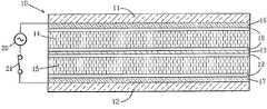
제1(a)도 및 제1(b)도는 투명한 프론트 기판(11) 및 투명 또는 불투명한 리어 기판(12)를 포함하는 셀(10)의 단면도.1 (a) and 1 (b) are cross-sectional views of a cell (10) comprising a transparent front substrate (11) and a transparent or opaque rear substrate (12).
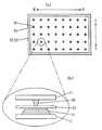
제2도는 각각 기판(11 및 12) 상의 스페이서(30, 31)의 정렬을 도시함.2 shows the alignment of the
제3(a)도는 셀이 어셈블리될 때 스페이서(30,31)이 어떻게 겹치는지를 도시하고, 제3(b)도는 중간 기판(13)이 스페이서(30 및 31)의 교차점의 위치에서 효과적으로 클램프된 점에서 셀을 통한 부분을 상세히 도시함.FIG. 3 (a) shows how the
제4도는 고체 물체와 접촉하고 있지 않은 표면을 갖는 플랫을 핸들링하고 유지하도록 막을 사용하는 지지 프레임(35)에 장착된 중간 기판(13)을 도시함.4 shows an
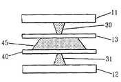
제5(a)도는 프론트 기판(11), 리어 기판(12) 및 2개의 중간 기판(13 및 40)을 포함하는 3개의 구획 셀의 스페이서 겹침 영역의 상세한 단면도를 도시하고, 제5(b)도는 프론트 기판(11), 리어 기판(12) 및 3개의 중간 기판(13,40 및 41)을 포함하는 4개의 구획 셀의 스페이서 겹침 영역의 상세한 단면도를 도시함.FIG. 5 (a) shows a detailed cross-sectional view of the spacer overlapping region of three compartment cells comprising the
* 도면의 주요부분에 대한 부호의 설명* Explanation of symbols for main parts of the drawings
10 : 셀 11 : 프론트 기판10 cell 11: front substrate
12 : 리어 기판 13 : 중간 기판12
14,15 : 구획 16 : 도전 물질14,15: compartment 16: conductive material
17 : 전극 18,19 : 정렬층17
20 : 외부 소스 21 : 스위치20: external source 21: switch
제1(a)도 및 제1(b)도는 투명한 프론트 기판(11) 및 투명 또는 불투명한 리어 기판(12)를 포함하는 셀(10)의 단면도를 도시한다. 매우 얇은 중간 기판(13)은 기판(11 과 12) 사이에 지탱되어, 액정 물질로 채워진 2개의 구획(14 및 15)를 형성한다. 기판(11)은 이들 내부면 상에 전기적으로 투명한 도전 물질(16)으로 덮혀진다. 기판(12)는 내부면 상에 전기적으로 투명 또는 불투명한 도전 물질로 제조된 다수의 전극(17)로 덮혀진다. 불투명한 도전 물질은 반사되거나 광 흡수될 수 있다. 액정에 노출된 16, 17 및 13의 표면은 정렬 물질로 덮혀지고, 액정의 정렬을 허용하기 위해 기술에 공지된 어떤 다른 방식으로 러브 또는 처리될 수 있다. 셀의 상부 부분의 정렬층(18)은 하부 부분의 정렬층(19)과 동일하거나 다를 수 있다. 전계는 외부 소스(20) 및 스위치(21)에 의해 층(16과 17) 사이에 인가될 수 있다. 제1(a)도는 필드 오프 상태에서의 셀을 도시한다. 셀의 상부 및 하부 부분의 새딩은 기판의 평면과 실질적으로 평행하고, 상부 부분의 페이지 평면과 수직이며, 하부 부분의 페이지 평면과 평행하게 정렬된 액정을 도시하기 위해 의도된다. 제1(b)도는 필드 온 상태에서의 셀을 도시하고, 모든 액정 물질을 기판 평면과 실질적으로 수직으로 정렬된다.1 (a) and 1 (b) show cross-sectional views of a
제2도는 각각 기판(11 및 12) 상의 스페이서(30,31)의 정렬을 도시한다. 여기에 도시된 스페이서의 크기 및 수 및 다음 도면은 목적만을 설명하기 위한 것으로, 스페이서의 실제 크기 및 수를 나타내지 않는다. 또, 제2도는 접착제(32 및 33)가 엣지 밀봉을 형성하기 위해 11 및 12의 주변을 둘러싸 미리 차단되는 가능한 방법을 도시한다. 이 방법은 액정 정렬용 외에 얇은 중간 기판(13)을 처리하여야 할 어떠한 필요성도 가리지 않는다.2 shows the alignment of the
제3(a)도는 셀이 어셈블리될 때 스페이서(30,31)이 어떻게 겹치는지를 도시한다. 제3(b)도는 중간 기판(13)이 스페이서(30 및 31)의 고차점의 위치에서 효과적으로 클램프된 점에서의 셀의 단면을 상세히 도시한다.3 (a) shows how
제4도는 고체 물체와 접촉하고 있지 않은 표면을 갖는 플랫을 핸들링하고 유지하도록 막을 사용하는 지지 프레임(35)에 장착된 중간 기판(13)을 도시한다. 13은 접착제로 35에 고정될 수 있고, 적합한 균일 텐션하에서 어느 다른 적합한 수단으로 기계적으로 클램프 또는 유지될 수 있다. 셀 어셈블리시, 상부 및 하부 기판(11,12)는 이들 사이의 위치에 13을 갖고 서로에 대해 정렬된다. 적합한 기계 수단에 의해, 이것은 화살표로 도시된 바와 같이 접촉부로 이동된 다음, 셀은 주변 접착제를 큐어링(curing) 함으로써 밀봉된다.4 shows an
제5(a)도는 프론트 기판(11), 리어 기판(12) 및 2개의 중간 기판(13 및 40)을 포함하는 3개의 구획 셀의 스페이서 겹침 영역의 상세한 단면도를 도시한다. 스페이서(30,31 및 45)는 각각 기판(11,12 및 40)에 증착된다. 제5(b)도는 프론트 기판(11), 리어 기판(12) 및 3개의 중간 기판(13,40 및 41)을 포함하는 4개의 구획 셀의 스페이서 겹침 영역의 상세한 단면도를 도시한다. 스페이서(30,31)은 각각 기판(11 및 12)에 증착된다. 또, 스페이서(45,46)의 증착을 위해 2개의 선택 구조가 도시되어 있다. 제5(b)도의 좌측 도면에서, 스페이서(45 및 46)은 각각 기판(40 및 41) 상에 증착된다. 우측 도면에서, 스페이서(45,46)은 기판(40)의 대향하는 측에 증착된다.FIG. 5 (a) shows a detailed cross-sectional view of the spacer overlapping region of three compartment cells comprising a
제1도는 이중 액정 셀(10)의 단면도를 도시하는 것으로, 투명한 프론트 기판(11) 및 투명 또는 불투명한 리어 기판(12)는 투명한 중간 기판 또는 막(13)에 의해 분리되고, 이격된다. 기판(11)의 내부면은 투명한 전극 물질(16),. 예를 들면 인듐 틴옥사이드(ITO)로 덮혀진다. 리어 기판의 내부면은 사용된 특정한 액정 효과에 따라 투명 또는 불투명, 반사 또는 광 흡수될 수 있는 전극 물질(17)로 덮혀진다. 사용된 특정한 액정 효과에 의존하다. 본 발명은 이것을 형성하는 새로운 셀 구조물 및 방법에 관한 것이다. 이것은 몇 개의 다른 액정 효과 및 몇 개의 다른 어드레싱 설계로 사용될 수 있다. 예를 들면, 높은 해상도 디스플레이에서 단안정 액정 효과를 사용할 때, 화소는 각 화소가 트랜지스터, 다이오드 또는 금속/절연체/금속(MIM) 디바이스일 수 있는 집적 회로 스위치를 통해 구동된 액티브 매트릭스에 의해 어드레스 될 수 있다. 모든 이러한 경우에서, 컨덕터(17)은 각각 하나의 화소를 위한 다수의 전극으로 에치될 수 있다. TFT 구동 디스플레이의 경우에서, 전극(16)은 연속적인 시트이고, 다이오드 및 MIM의 경우에, 전극은 디스플레이의 각 컬럼의 스트립으로 에치될 수 있다. PSCT와 같은 쌍안정 액정 효과의 경우에, 액티브 매트릭스는 불필요해질 수 있다. 결과적으로, 16은 컬럼 스트립으로 에치될 수 있고, 17은 16과 대각선 방향으로 로우 스트립으로 에치될 수 있다. 네마틱 게스트-호스트 효과는 이 명세서의 나머지 예로서 사용될 수 있다. 이 효과는 액티브 매트릭스로 어드레스되기에 적합하고, 전극(17)은, 예를 들면 알루미늄과 같은 높은 반사 금속으로 형성될 수 있다. 선택적으로, 이것은 투명한 도전 물질로 덮혀진 유전체 미러 스택으로 제조될 수 있다. 제2도를 참조하면, 스페이서(30,31)은 기판(11 및 12) 상에 증착된다. 스페이서는 기판(11 및 12)가 결합될 때, 대향 기판 상의 스페이서 쌍이 제3도에 도시한 바와 같이 겹치도록 정확하게 배치된다. 이러한 스페이서를 증착하는 몇가지 기술 방법이 있다. 양호한 방법은 필요한 스페이서 높이와 실질적으로 두께가 동일한 폴리이미드와 같은 폴리머로 기판을 덮는 것이다. 막은 큐어(cure)된 다음, 포토리소그래픽 방법으로 패턴화되고, 반응성 이온 에칭 프로세스로 에치되어, 필요한 스페이서를 남긴다. 스페이서의 크기는 사용된 액정 효과, 화소 피치 및 셀 어셈블리시 기판을 정렬하는데 사용된 툴링(tooling)의 정확성에 결정될 수 있다. 이 예에서, 이들 형태 및 크기는 11 및 12의 정렬 정확성이 최소화되고, 스페이서가 화소간 갭 내에 숨겨지도록 폭이 충분히 좁도록 선택된다. 그러나, 본 발명은 도시된 특정 크기 및 형태에 제한되지 않고, 모든 적합한 선택적인 크기 및 형태가 사용될 수 있다. 현재 경우의 전형적인 값은 높이가 3과 10㎛사이이고, 길이가 20과 250㎛사이이며, 폭이 화소간 갭(5-20㎛)보다 작게 될 수 있다. 화소간 갭 내에 스페이서를 배치하는 것은 디스플레이의 표시 성능을 방해하거나 열화시키지 않는 장점이 있다. 이 기판은 폴리이미드와 같은 정렬 폴리머의 얇은 층(수십 나노미터 두께)이 스핀 코드된 다음, 양호하게 스페이서의 긴 축 방향으로 큐어되고, 러브된다.FIG. 1 shows a cross-sectional view of the dual
중간 기판은 핸들링 및 처리 필요성에 따라 가능한 한 얇아야 하는 폴리머막이다. 양호한 실시예는 0.9㎛이하의 두께로 사용 가능한 듀폰사에 의해 제조된 폴리에스테르막인 마일라(Mylar : TM)이지만, 필요한 광학 및 기계적 특성을 갖는 임의의 막도 사용될 수 있다. 또, 폴리이미드, 폴리아미드 및 폴리아크릴레이트와 같은 기타 폴리머막(이들에 한정되지 않음) 및 매우 얇은 글라스, 산화물 또는 다른 투명한 유전체막들도 전술한 핸들링 및 공정 조건내에서 적합할 수 있다. 마일라는 이 명세서에서 양호한 물질로서 사용될 수 있다. 제4도를 참조하면, 마일라(13)의 시트는 광에서 균일 텐션이 유지해지도록 접착제 또는 기계 수단 중 하나에 의해 결고한 평면 프레임(35)에 부착된다. 그 다음, 이렇게 장착된 막은 약 섭씨 200도까지 가열 사이클로 처리된다. 이것은 막의 영구 수축을 야기시켜 막을 팽팽하고 평평하게 한다. 마일라막은 광학적으로 이방성이고, 현재 예를 위해서는 액정이 광축과 평행하거나 수직으로 정렬되는 것이 중요하다. 축 방향은 교차된 편광 프리즘 사이에서 막을 조사하는 소정의 적합한 방법에 의해 결정될 수 있으나, 실제로는 막이 벌크 롤(bulk roll)로부터 절단되는 제조 공정에서, 광축의 방향은 실질적으로 일정해질 수 있으므로 모든 샘플에 대하여 축방향을 결정할 필요는 없다. 그 다음, 막은 정렬 처리된다. 막의 핸들링 특성과 일치하는 어떠한 처리도 사용될 수 있다. 비접촉 방법이 바람직하지만, 접촉 방법도 제외되지 않는다. 비접촉 방법의 예는 막의 양측에 얇은 폴리이미드 정렬층을 스핀 코팅한 다음, 13의 2개의 표면에 직교하는 정렬 방향을 형성하기 위해 적합한 방향으로 각 표면에 콜리메이트(collimated)된 자외선을 조사하는 것이다.The intermediate substrate is a polymer film that should be as thin as possible depending on the handling and processing needs. A preferred embodiment is Mylar (TM), a polyester film made by DuPont available with a thickness of 0.9 μm or less, but any film having the necessary optical and mechanical properties may be used. In addition, other polymer films such as, but not limited to, polyimides, polyamides, and polyacrylates, and very thin glass, oxide, or other transparent dielectric films may also be suitable within the handling and processing conditions described above. Mylar can be used as a good material in this specification. Referring to FIG. 4, the sheet of
그러나, 막(13)에 정렬층을 예비코팅하는 필요성 및 접촉부를 러빙하는 필요성을 회피하는 양호한 방법은 13의 2개 표면에 요구되는 직교하는 정렬 방향, 즉, 광축에 대해 평행 및 수직의 정렬 방향을 제공하기 위한 방향에서 기판에 대해 45°내지 85°의 입사각으로 아르곤 이온과 같은 낮은 에너지 이온의 빔을 막의 양면에 조사하는 것이다. 이것을 행하기 위해, 얇은 마일라 시트는 프레임을 가로질러 스크래치된다. 막은 프리-스탠딩(free-standing) 상태이다. 마일라는 직접 조사된다. 폴리이미드는 마일라 상에 스펀되지 않음에 주의한다. 따라서, 우리는 마일라, 프리스탠딩막, 프레임 및 이들의 디스플레이내에서의 사용을 보호한다. 이러한 방법은 본 발명의 양수인에게 양수되고, 여기에서 참조 문헌으로 사용된 Chaudhari 등에 의한 ″Atomic Beam Alignment of Liquid Crystals″란 제목으로 동일 날짜에 제출된 미합중국 특허 출원 번호__________에 설명되어 있다.However, a preferred method of avoiding the need to precoat the alignment layer on the
제2도를 참조하면, 접착제(32,33)은 기판(11 및 12) 주변을 둘러싸 증착된다. 실제로, 차후에 셀을 채울 수 있는 개구를 형성하기 위해 접착제에 갭이 남겨진다. 기판(12)는 정렬 툴에 배치된다. 아직 프레임(35)에 부착된 막(13)은 12로 하향된다. 그 다음, 기판(11)은 스페이서(30,31)이 제3도에 도시한 바와 같이 겹치도록 배치된다. 이것은 13 및 12로 하향되어, 13 및 12와 접촉된 다음, 접착제는 큐어된다. 마일라막(13)은 주변 접착제 밀봉에 의해 장력을 받도록 유지되고, 셀 스페이싱은 막이 각 스페이서 교차점에서 스페이서 사이에 클램프되기 때문에 필요한 정도의 정밀도로 유지된다. 스페이서의 밀도는 요구조건이 충족되도록 조정될 수 있다. 여분의 마일라는 셀의 주위를 따라 잘려내어지고, 셀은 네마틱 게스트-호스트 혼합물로 채워진다. 동일 혼합물이 셀의 양 구획(14,15)에 사용되기 때문에, 변부의 충진홀은 인접할 수 있다. 다른 예에서, 다른 액정 혼합물이 각 구획에 사용될 때, 충진홀은 양호하게는 디스플레이의 대향측에 위치하도록 충분히 분리되어야만 한다. 셀은 디스플레이의 모든 지점의 스페이서 교차점에서 포지티브 접촉이 발생하는 것을 보장하기 위해 초과 외부 압력으로 유지되고, 충진 홀은 접착제 또는 기타 적합한 물질로 밀봉된다.Referring to FIG. 2,
셀의 구조는 필드 오프 상태에서, 구획(14)가 제3도의 화살표 H-H 방향으로 편광된 광을 효과적으로 흡수할 수 있는 트위스트되지 않은 균일하게 정렬된 네마틱 게스트-호스트층을 포함한다. 구획(15)는 구획(14)와 직교하는 정렬 방향을 갖는 유사한 네마틱 게스트-호스트층을 포함한다. 이 층은 화살표 V-V의 방향으로 편광된 광을 효과적으로 흡수한다. 따라서, 셀은 이것에 입사하는 모든 광을 효과적으로 흡수한다. 필드가 기판(11과 12) 사이의 셀을 가로질러 인가될 때, 포지티브 유전체 이방성을 갖는 액정 분자는 디스플레이의 평면과 실질적으로 수직으로 회전한다. 이러한 방향성을 가질 때, 다이 분자에 의한 입사 광의 흡수는 최소화되고, 디스플레이의 반사성이 커지게 된다. 이 디스플레이는 예1의 공기 기술의 매우 낮은 필드 오프 상태 반사율 및 낮은 구동 전압, 및 예2의 공지 기술의 높은 필드 온 상태 반사율을 가지게 된다. 매우 얇은 중간 기판(13)이 사용되기 때문에, 효과적으로 셀의 상부 및 하부 구획에 형성된 화상들 사이에 패럴렉스는 없다. 온 상태의 반사율이 60%를 초과할 때 12 : 1 이상의 콘트라스트비가 달성될 수 있다.The structure of the cell includes a non-twisted uniformly aligned nematic guest-host layer that, in the field off state,
본 실시예는 인가된 전계의 방향과 평행한 분자로 정렬된 포지티브 유전체 이방성을 갖는 네마틱 물질의 사용에 관한 것이다.This example relates to the use of nematic materials with positive dielectric anisotropy aligned in molecules parallel to the direction of the applied electric field.
스택된 게스트-호스트 효과의 다른 실시예는 인가된 전계 방향과 수직인 분자로 정렬된 네가티브 유전체 이방성을 갖는 네마틱 물질의 사용에 관한 것이다.Another embodiment of the stacked guest-host effect relates to the use of nematic materials with negative dielectric anisotropy aligned with molecules perpendicular to the direction of the applied field.
이 실시예의 일반적인 셀 구조 및 특징은 먼저 설명한 실시예에 대해서와 실질적으로 동일하다. 다른 점은 제1(a)도의 정렬층(18)이 제3(a)도에 화살표 H-H의 방향으로 경사 바이어스가 작은 구획(14)에서 액정 분자의 수직 정렬을 실질적으로 발생하기 위한 것이다. 유사한 형태로, 제1(a)도의 정렬층(19)은 제3(a)도의 화살표 V-V의 방향으로 경사 바이어스가 작은 구획(15)에서 액정 분자의 수직 정렬을 실질적으로 발생하기 위한 것이다. 따라서, 디스플레이의 필드 오프 상태는 밝아진다. 전계가 기판(11과 12) 사이에 인가될 때, 액정 분자는 구획(14)에서 기판과 실질적으로 평행하고, 방향 H-H과 평행하게 정렬하며, 구획(15)에서 V-V와 평행하게 정렬한다. 따라서, 이 실시예의 필드 온 상태는 어두워진다. 경사 바이어스를 갖는 수직 정렬을 형성하는 방법은 기술에 공지되어 있지만, 여기에 요구되지 않는다. 이 실시예에 의해 달성 가능한 반사율 및 콘트라스트 비는 실시예 1에서 달성가능한 것과 실질적으로 동일하지만, 이 실시예는 제1 양호한 실시예의 경우에서 어둡게 되는 것과 반대로 필드 오프 상태에서 밝게 된다.The general cell structure and features of this embodiment are substantially the same as for the previously described embodiment. Another difference is that the
본 발명의 다른 실시예는 액정층이 종래 기술의 예3에서 토론된 바와 같이 스스로 광을 반사하는 효과에 관한 것이다. 여기에서, 셀 구조물은 제1 양호한 실시예에서의 셀 구조와 실질적으로 동일하다. 그러나, 이 경우에 중간 기판(13)의 필요한 특성을 다르게 된다. 구획(14 및 15)는 대항하는 트위스트 센스, 예를 들면 14에서 오른쪽으로 도는 트위스트층 및 15에서 왼쪽으로 도는 트위스트층을 갖는 치랄 네마틱 물질로 채워진다. 따라서, 14에 의해 투과된 광은 원형으로 편광될 수 있고, 이 편광 상태는 15의 물질에 의해 광이 반사될 때의 상태로서 보존되어야 한다. 따라서, 13은 실질적으로 광학적으로 동방성이어야만 한다. 즉, 이것은 실질적으로 제로 복굴절을 갖는다. 마일라막의 경우에, 이것은 단일막으로 달성하기 어렵다. 그러나, 한 막의 복굴절이 다른 것에 의해 제거될 수 있기 때문에, 서로 직교하는 방향성을 가진 2개의 실질적으로 동일한 복굴절막은 필요한 광학적 특성을 달성할 수 있다. 적합한 합성막은 이들 사이의 공간을 진공화하여 2개의 이러한 막을 간단히 결합하여 제조될 수 있다. 그 다음, 이것은 표면력의 작용에 의해 긴밀한 접촉을 유지할 수 있다. 선택적으로, 막의 평면에서 실질적으로 동방성인 막은 고체 또는 액체일 수 있는 폴리머 물질을 주조하거나 스핀 코팅하고, 큐어링하고 기판으로부터 분리함으로써 제조될 수 있다. 셀은 분리된 2개의 구획의 충진 홀 및 우측 물질 및 좌측 물질로 따로따로 채워진 구획을 갖는 제1 양호한 실시예에서와 실질적으로 동일 방법으로 처리된다. 정렬 요구조건은 사용되는 효과의 성질에 따라 다르지만, 종래 기술에 이미 공지되어 있다. 여기에 설명한 바와 같은 셀은 종래 기술에 따른 셀에 비하여 대략 두배의 반사율을 나타낼 수 있다.Another embodiment of the present invention relates to the effect of the liquid crystal layer reflecting light by itself as discussed in Example 3 of the prior art. Here, the cell structure is substantially the same as the cell structure in the first preferred embodiment. In this case, however, the necessary properties of the
또, 본 발명의 다른 실시예는 액정층이 광을 반사하는 효과의 사용에 관한 것이다. 여기에서, 중간 기판(13)의 복굴절은 광축과 평행하고 수직인 광경로 길이가 광의 1/2 파장만큼 다르도록 광학적 이방성을 조정함으로써 활용된다. 이 경우에, 구획(14 및 15)는 동일한 치랄 네마틱 물질로 채워진다. 우리는 우측 물질을 예를 들어 설명하였지만, 이 설명은 좌측 물질에도 동일하게 적응된다. 14에 의해 투과된 좌측 원형 편광 광은 13을 통한 투과로 우측 원형 편광 광으로 변환되고, 15에 의해 반사된다. 이것이 스펙트럼의 가시 영역에서 정확히 1/2파 리타더(retarder)인 막을 형성하기 어렵기 때문에, 이 예의 성능은 선행하는 예의 성능보다 열등해질 수 있다.Another embodiment of the present invention also relates to the use of the effect that the liquid crystal layer reflects light. Here, the birefringence of the
본 발명의 또 다른 실시예는 2 이상의 구획을 필요로 하는 디스플레이를 포함한다. 예를 들면, 미합중국 특허 5,200,845에서 Crooker 등에 의해 설명된 것과 유사한 스택된 칼라 셀에 대한 본 발명의 응용은 총 6개의 구획을 필요로 할 수 있다. 그러나, 2이상의 다수 구획을 사용하는 모든 경우에 적용되는 원리는 유사한다. 이러한 경우에, 스페이서는 적합한 수의 중간 기판의 표면에 증착되어야 한다. 제5(a)도를 참조하면, 3개의 구획 셀은 그 위에 스페이서(45)가 처리되어야 하는 추가 중간 기판(40)을 사용함으로서 제조된다. 이 구조에서, 기판(12)에 증착된 스페이서(31)은 2개의 구획 셀에 대하여 수직 방향으로 회전됨에 주의한다.Another embodiment of the invention includes a display requiring two or more compartments. For example, the application of the present invention to stacked color cells similar to that described by Crooker et al. In US Pat. No. 5,200,845 may require a total of six compartments. However, the principle applied in all cases using two or more multiple compartments is similar. In this case, the spacer must be deposited on the surface of a suitable number of intermediate substrates. Referring to FIG. 5 (a), three compartment cells are fabricated by using an additional
제5(b)도는 4개의 구획 셀을 도시한다. 여기에서, 중간 기판(40,41)에 스페이서를 증착하는 2가지 선택적 방법이 있다. 한 세트의 스페이서는 각각[각각 기판(40,41) 상의 스페이서(45,46)](좌측 도시)에 증착될 수 있거나, 양 세트의 스페이서(45,46)은 기판(40)(우측 도시)에서 처리될 수 있다. 앞의 절차는 처리 관점에서 더 간단해질 수 있지만, 후자는 정확하게 정렬되어야만 하는 기판 수가 4에서 3으로 감소함으로서 셀 어셈블 리가 더 간단해질 수 있다.5 (b) shows four compartment cells. Here, there are two alternative ways of depositing spacers on the
이와 같이 본 발명은 상술한 실시 형태에 한정되지 않고, 본 발명의 지시를 이탈하지 않은 범위에서 여러 가지 구성을 취할 수 있다.Thus, this invention is not limited to embodiment mentioned above, A various structure can be taken in the range which does not deviate from the indication of this invention.
Claims (30)
Translated fromKoreanApplications Claiming Priority (2)
| Application Number | Priority Date | Filing Date | Title |
|---|---|---|---|
| US08/644,556US5801796A (en) | 1996-05-10 | 1996-05-10 | Stacked parallax-free liquid crystal display cell |
| US8/644,556 | 1996-05-10 |
Publications (1)
| Publication Number | Publication Date |
|---|---|
| KR100232510B1true KR100232510B1 (en) | 1999-12-01 |
Family
ID=24585410
Family Applications (1)
| Application Number | Title | Priority Date | Filing Date |
|---|---|---|---|
| KR1019970010303AExpired - LifetimeKR100232510B1 (en) | 1996-05-10 | 1997-03-25 | Stacked parallax-free lcd cell |
Country Status (4)
| Country | Link |
|---|---|
| US (1) | US5801796A (en) |
| JP (1) | JP3177186B2 (en) |
| KR (1) | KR100232510B1 (en) |
| DE (1) | DE19711827C2 (en) |
Families Citing this family (26)
| Publication number | Priority date | Publication date | Assignee | Title |
|---|---|---|---|---|
| US6094244A (en)* | 1995-12-27 | 2000-07-25 | Kabushiki Kaisha Toshiba | Reflective liquid crystal display device |
| US6034752A (en) | 1997-03-22 | 2000-03-07 | Kent Displays Incorporated | Display device reflecting visible and infrared radiation |
| JP3974217B2 (en)* | 1997-04-02 | 2007-09-12 | シャープ株式会社 | Liquid crystal display panel and liquid crystal display device |
| WO1998057226A2 (en)* | 1997-06-12 | 1998-12-17 | Zetfolie B.V. | Substrate having a unidirectional conductivity perpendicular to its surface, devices comprising such a substrate and methods for manufacturing such a substrate |
| JP3147156B2 (en)* | 1997-11-18 | 2001-03-19 | 富士ゼロックス株式会社 | Display storage medium, image writing method, and image writing device |
| GB2334111A (en)* | 1998-02-04 | 1999-08-11 | Ibm | High reflectivity liquid crystal display cell |
| US6459467B1 (en)* | 1998-05-15 | 2002-10-01 | Minolta Co., Ltd. | Liquid crystal light modulating device, and a manufacturing method and a manufacturing apparatus thereof |
| JP2000178557A (en)* | 1998-12-14 | 2000-06-27 | Minolta Co Ltd | Liquid crystal composition and liquid crystal light modulation element |
| GB2345979A (en)* | 1999-01-23 | 2000-07-26 | Ibm | High reflectivity bistable liquid crystal display |
| US6803899B1 (en)* | 1999-07-27 | 2004-10-12 | Minolta Co., Ltd. | Liquid crystal display apparatus and a temperature compensation method therefor |
| DE60042549D1 (en)* | 2000-02-22 | 2009-08-27 | Asulab Sa | A contrast inversion display unit comprising two superimposed display devices |
| JP4712210B2 (en)* | 2000-03-24 | 2011-06-29 | 株式会社半導体エネルギー研究所 | Display device |
| DE10023282A1 (en)* | 2000-05-12 | 2001-11-15 | Mannesmann Vdo Ag | Liquid crystal display device for automobile uses 2 active liquid crystal display cells with one providing color compensation for other |
| US6680726B2 (en) | 2001-05-18 | 2004-01-20 | International Business Machines Corporation | Transmissive electrophoretic display with stacked color cells |
| US6727873B2 (en) | 2001-05-18 | 2004-04-27 | International Business Machines Corporation | Reflective electrophoretic display with stacked color cells |
| US6781566B2 (en)* | 2001-08-22 | 2004-08-24 | Aurora Systems, Inc. | Residual DC bias correction in a video imaging device |
| CN100451777C (en)* | 2004-04-21 | 2009-01-14 | 统宝光电股份有限公司 | Transmissive LCD |
| US20060066803A1 (en)* | 2004-09-30 | 2006-03-30 | Aylward Peter T | Substrate free flexible liquid crystal displays |
| EP1832027A1 (en)* | 2004-12-21 | 2007-09-12 | Koninklijke Philips Electronics N.V. | Display device for visually reconstructing an image |
| KR20080014317A (en)* | 2006-08-10 | 2008-02-14 | 삼성전자주식회사 | Display device and manufacturing method thereof |
| JP4545183B2 (en)* | 2006-11-20 | 2010-09-15 | 三洋電機株式会社 | Liquid crystal display device and device with display function |
| KR20100004031A (en)* | 2008-07-02 | 2010-01-12 | 삼성전자주식회사 | Transparent display device and manufacturing method thereof |
| US9135864B2 (en) | 2010-05-14 | 2015-09-15 | Dolby Laboratories Licensing Corporation | Systems and methods for accurately representing high contrast imagery on high dynamic range display systems |
| EP2684184A4 (en) | 2011-03-09 | 2014-08-13 | Dolby Lab Licensing Corp | HIGH CONTRAST COLOR GRAVEL SCALE DISPLAYS |
| GB2585190B (en)* | 2019-06-28 | 2023-06-14 | Flexenable Tech Limited | Liquid crystal device comprising stack of at least two liquid crystal cells in optical series |
| DE102021112947A1 (en) | 2021-05-19 | 2022-11-24 | Sioptica Gmbh | Optical element with variable transmission and screen with such an optical element |
Family Cites Families (17)
| Publication number | Priority date | Publication date | Assignee | Title |
|---|---|---|---|---|
| DE2459488A1 (en)* | 1974-12-16 | 1976-06-24 | Siemens Ag | LIQUID CRYSTAL COMPOSITE DISPLAY SCREEN (CELL) |
| DE2404127C3 (en)* | 1974-01-29 | 1979-05-17 | Siemens Ag, 1000 Berlin Und 8000 Muenchen | Liquid crystal display |
| JPS575029A (en)* | 1980-06-12 | 1982-01-11 | Seiko Epson Corp | Liquid crystal display device |
| NZ198241A (en)* | 1980-09-27 | 1983-12-16 | Beecham Group Ltd | Tablet containing amoxycillin and potassium clavulanate |
| JPH0748094B2 (en)* | 1987-12-25 | 1995-05-24 | シャープ株式会社 | Color liquid crystal display |
| JPH01309024A (en)* | 1988-06-08 | 1989-12-13 | Ube Ind Ltd | liquid crystal display device |
| US4886343A (en)* | 1988-06-20 | 1989-12-12 | Honeywell Inc. | Apparatus and method for additive/subtractive pixel arrangement in color mosaic displays |
| JPH03122619A (en)* | 1989-10-05 | 1991-05-24 | Sharp Corp | color liquid crystal display device |
| US5200845A (en)* | 1989-10-31 | 1993-04-06 | University Of Hawaii At Manoa | Color liquid crystal display consisting of polymer-dispersed chiral liquid crystal having negative dielectric anisotropy |
| US5113272A (en)* | 1990-02-12 | 1992-05-12 | Raychem Corporation | Three dimensional semiconductor display using liquid crystal |
| JPH04199024A (en)* | 1990-11-29 | 1992-07-20 | Hitachi Ltd | Liquid crystal display element and display device using the same |
| US5453863A (en)* | 1991-05-02 | 1995-09-26 | Kent State University | Multistable chiral nematic displays |
| ATE178645T1 (en)* | 1991-05-02 | 1999-04-15 | Univ Kent State Ohio | LIQUID CRYSTAL LIGHT MODULATING DEVICE AND MATERIAL |
| JP2758287B2 (en)* | 1991-07-15 | 1998-05-28 | シャープ株式会社 | Liquid crystal display |
| DE69229003T2 (en)* | 1992-05-18 | 1999-10-21 | Kent State University, Kent | LIQUID CRYSTALINE, LIGHT-MODULATING DEVICE AND MATERIAL |
| US5251048A (en)* | 1992-05-18 | 1993-10-05 | Kent State University | Method and apparatus for electronic switching of a reflective color display |
| JP2945572B2 (en)* | 1993-12-10 | 1999-09-06 | シャープ株式会社 | Liquid crystal display device and manufacturing method thereof |
- 1996
- 1996-05-10USUS08/644,556patent/US5801796A/ennot_activeExpired - Lifetime
- 1997
- 1997-03-21DEDE19711827Apatent/DE19711827C2/ennot_activeExpired - Fee Related
- 1997-03-25KRKR1019970010303Apatent/KR100232510B1/ennot_activeExpired - Lifetime
- 1997-05-08JPJP11849397Apatent/JP3177186B2/ennot_activeExpired - Lifetime
Also Published As
| Publication number | Publication date |
|---|---|
| US5801796A (en) | 1998-09-01 |
| DE19711827A1 (en) | 1997-11-20 |
| DE19711827C2 (en) | 1999-09-09 |
| JP3177186B2 (en) | 2001-06-18 |
| JPH1048662A (en) | 1998-02-20 |
Similar Documents
| Publication | Publication Date | Title |
|---|---|---|
| KR100232510B1 (en) | Stacked parallax-free lcd cell | |
| US9280018B2 (en) | Multistable reflective liquid crystal device | |
| JP2551932B2 (en) | Liquid crystal display | |
| US4114990A (en) | Liquid crystal rotator | |
| KR920009824B1 (en) | Liquid crystal display device | |
| US5880798A (en) | Twisted nematic liquid crystal device | |
| EP2614404A1 (en) | Switchable privacy filter | |
| JP2000214466A (en) | Bistable liquid crystal display device having high reflectance | |
| JP2024022690A (en) | Optical laminates, image display devices and glass composites | |
| KR20080026599A (en) | Stacked type reflective liquid crystal display device | |
| KR100663074B1 (en) | Reflective type liquid crystal display device including retardation layer | |
| US3966304A (en) | Liquid crystal display device | |
| JP2002169155A (en) | Liquid crystal display device | |
| JP3620312B2 (en) | Liquid crystal display | |
| KR100476600B1 (en) | Liquid crystal display with reflection mode and transmission mode | |
| JP3915490B2 (en) | Liquid crystal display | |
| JP2023521536A (en) | Optical device containing optically anisotropic molecules with intermediate pretilt angles | |
| JP3294210B2 (en) | High reflectance liquid crystal display cell | |
| JP3367853B2 (en) | Reflective liquid crystal display | |
| WO2009080119A1 (en) | Liquid crystal display | |
| KR20220003720A (en) | Viewing angle variable element and display assembly | |
| JPH07159805A (en) | Liquid crystal display device and manufacturing method thereof | |
| JP2927274B2 (en) | Elliptical polarizing plate and liquid crystal display using the same | |
| JP3583250B2 (en) | Reflective liquid crystal display | |
| KR100224699B1 (en) | LCD |
Legal Events
| Date | Code | Title | Description |
|---|---|---|---|
| PA0109 | Patent application | Patent event code:PA01091R01D Comment text:Patent Application Patent event date:19970325 | |
| A201 | Request for examination | ||
| PA0201 | Request for examination | Patent event code:PA02012R01D Patent event date:19970829 Comment text:Request for Examination of Application Patent event code:PA02011R01I Patent event date:19970325 Comment text:Patent Application | |
| PG1501 | Laying open of application | ||
| E701 | Decision to grant or registration of patent right | ||
| PE0701 | Decision of registration | Patent event code:PE07011S01D Comment text:Decision to Grant Registration Patent event date:19990809 | |
| GRNT | Written decision to grant | ||
| PR0701 | Registration of establishment | Comment text:Registration of Establishment Patent event date:19990906 Patent event code:PR07011E01D | |
| PR1002 | Payment of registration fee | Payment date:19990907 End annual number:3 Start annual number:1 | |
| PG1601 | Publication of registration | ||
| PR1001 | Payment of annual fee | Payment date:20020830 Start annual number:4 End annual number:4 | |
| PR1001 | Payment of annual fee | Payment date:20030829 Start annual number:5 End annual number:5 | |
| PR1001 | Payment of annual fee | Payment date:20040831 Start annual number:6 End annual number:6 | |
| PR1001 | Payment of annual fee | Payment date:20051024 Start annual number:7 End annual number:7 | |
| PR1001 | Payment of annual fee | Payment date:20060906 Start annual number:8 End annual number:8 | |
| PR1001 | Payment of annual fee | Payment date:20070831 Start annual number:9 End annual number:9 | |
| PR1001 | Payment of annual fee | Payment date:20080901 Start annual number:10 End annual number:10 | |
| PR1001 | Payment of annual fee | Payment date:20090902 Start annual number:11 End annual number:11 | |
| PR1001 | Payment of annual fee | Payment date:20100827 Start annual number:12 End annual number:12 | |
| PR1001 | Payment of annual fee | Payment date:20110824 Start annual number:13 End annual number:13 | |
| FPAY | Annual fee payment | Payment date:20120821 Year of fee payment:14 | |
| PR1001 | Payment of annual fee | Payment date:20120821 Start annual number:14 End annual number:14 | |
| FPAY | Annual fee payment | Payment date:20130819 Year of fee payment:15 | |
| PR1001 | Payment of annual fee | Payment date:20130819 Start annual number:15 End annual number:15 | |
| FPAY | Annual fee payment | Payment date:20140826 Year of fee payment:16 | |
| PR1001 | Payment of annual fee | Payment date:20140826 Start annual number:16 End annual number:16 | |
| FPAY | Annual fee payment | Payment date:20150819 Year of fee payment:17 | |
| PR1001 | Payment of annual fee | Payment date:20150819 Start annual number:17 End annual number:17 | |
| FPAY | Annual fee payment | Payment date:20160818 Year of fee payment:18 | |
| PR1001 | Payment of annual fee | Payment date:20160818 Start annual number:18 End annual number:18 | |
| EXPY | Expiration of term | ||
| PC1801 | Expiration of term |