KR100229507B1 - Switching mode power supplier having function of protecting circuit from abnormal voltage - Google Patents
Switching mode power supplier having function of protecting circuit from abnormal voltageDownload PDFInfo
- Publication number
- KR100229507B1 KR100229507B1KR1019970005239AKR19970005239AKR100229507B1KR 100229507 B1KR100229507 B1KR 100229507B1KR 1019970005239 AKR1019970005239 AKR 1019970005239AKR 19970005239 AKR19970005239 AKR 19970005239AKR 100229507 B1KR100229507 B1KR 100229507B1
- Authority
- KR
- South Korea
- Prior art keywords
- voltage
- unit
- signal
- switching
- output
- Prior art date
- Legal status (The legal status is an assumption and is not a legal conclusion. Google has not performed a legal analysis and makes no representation as to the accuracy of the status listed.)
- Expired - Fee Related
Links
Images


Classifications
- H—ELECTRICITY
- H02—GENERATION; CONVERSION OR DISTRIBUTION OF ELECTRIC POWER
- H02H—EMERGENCY PROTECTIVE CIRCUIT ARRANGEMENTS
- H02H7/00—Emergency protective circuit arrangements specially adapted for specific types of electric machines or apparatus or for sectionalised protection of cable or line systems, and effecting automatic switching in the event of an undesired change from normal working conditions
- H02H7/10—Emergency protective circuit arrangements specially adapted for specific types of electric machines or apparatus or for sectionalised protection of cable or line systems, and effecting automatic switching in the event of an undesired change from normal working conditions for converters; for rectifiers
- H02H7/12—Emergency protective circuit arrangements specially adapted for specific types of electric machines or apparatus or for sectionalised protection of cable or line systems, and effecting automatic switching in the event of an undesired change from normal working conditions for converters; for rectifiers for static converters or rectifiers
- H02H7/122—Emergency protective circuit arrangements specially adapted for specific types of electric machines or apparatus or for sectionalised protection of cable or line systems, and effecting automatic switching in the event of an undesired change from normal working conditions for converters; for rectifiers for static converters or rectifiers for inverters, i.e. DC/AC converters
- H02H7/1227—Emergency protective circuit arrangements specially adapted for specific types of electric machines or apparatus or for sectionalised protection of cable or line systems, and effecting automatic switching in the event of an undesired change from normal working conditions for converters; for rectifiers for static converters or rectifiers for inverters, i.e. DC/AC converters responsive to abnormalities in the output circuit, e.g. short circuit
- H—ELECTRICITY
- H02—GENERATION; CONVERSION OR DISTRIBUTION OF ELECTRIC POWER
- H02M—APPARATUS FOR CONVERSION BETWEEN AC AND AC, BETWEEN AC AND DC, OR BETWEEN DC AND DC, AND FOR USE WITH MAINS OR SIMILAR POWER SUPPLY SYSTEMS; CONVERSION OF DC OR AC INPUT POWER INTO SURGE OUTPUT POWER; CONTROL OR REGULATION THEREOF
- H02M3/00—Conversion of DC power input into DC power output
- H02M3/22—Conversion of DC power input into DC power output with intermediate conversion into AC
- H02M3/24—Conversion of DC power input into DC power output with intermediate conversion into AC by static converters
- H02M3/28—Conversion of DC power input into DC power output with intermediate conversion into AC by static converters using discharge tubes with control electrode or semiconductor devices with control electrode to produce the intermediate AC
- H02M3/325—Conversion of DC power input into DC power output with intermediate conversion into AC by static converters using discharge tubes with control electrode or semiconductor devices with control electrode to produce the intermediate AC using devices of a triode or a transistor type requiring continuous application of a control signal
- H02M3/335—Conversion of DC power input into DC power output with intermediate conversion into AC by static converters using discharge tubes with control electrode or semiconductor devices with control electrode to produce the intermediate AC using devices of a triode or a transistor type requiring continuous application of a control signal using semiconductor devices only
- H02M3/33507—Conversion of DC power input into DC power output with intermediate conversion into AC by static converters using discharge tubes with control electrode or semiconductor devices with control electrode to produce the intermediate AC using devices of a triode or a transistor type requiring continuous application of a control signal using semiconductor devices only with automatic control of the output voltage or current, e.g. flyback converters
- H02M3/33523—Conversion of DC power input into DC power output with intermediate conversion into AC by static converters using discharge tubes with control electrode or semiconductor devices with control electrode to produce the intermediate AC using devices of a triode or a transistor type requiring continuous application of a control signal using semiconductor devices only with automatic control of the output voltage or current, e.g. flyback converters with galvanic isolation between input and output of both the power stage and the feedback loop
- H—ELECTRICITY
- H02—GENERATION; CONVERSION OR DISTRIBUTION OF ELECTRIC POWER
- H02M—APPARATUS FOR CONVERSION BETWEEN AC AND AC, BETWEEN AC AND DC, OR BETWEEN DC AND DC, AND FOR USE WITH MAINS OR SIMILAR POWER SUPPLY SYSTEMS; CONVERSION OF DC OR AC INPUT POWER INTO SURGE OUTPUT POWER; CONTROL OR REGULATION THEREOF
- H02M1/00—Details of apparatus for conversion
- H02M1/0083—Converters characterised by their input or output configuration
- H02M1/009—Converters characterised by their input or output configuration having two or more independently controlled outputs
- H—ELECTRICITY
- H02—GENERATION; CONVERSION OR DISTRIBUTION OF ELECTRIC POWER
- H02M—APPARATUS FOR CONVERSION BETWEEN AC AND AC, BETWEEN AC AND DC, OR BETWEEN DC AND DC, AND FOR USE WITH MAINS OR SIMILAR POWER SUPPLY SYSTEMS; CONVERSION OF DC OR AC INPUT POWER INTO SURGE OUTPUT POWER; CONTROL OR REGULATION THEREOF
- H02M1/00—Details of apparatus for conversion
- H02M1/32—Means for protecting converters other than automatic disconnection
- H—ELECTRICITY
- H02—GENERATION; CONVERSION OR DISTRIBUTION OF ELECTRIC POWER
- H02M—APPARATUS FOR CONVERSION BETWEEN AC AND AC, BETWEEN AC AND DC, OR BETWEEN DC AND DC, AND FOR USE WITH MAINS OR SIMILAR POWER SUPPLY SYSTEMS; CONVERSION OF DC OR AC INPUT POWER INTO SURGE OUTPUT POWER; CONTROL OR REGULATION THEREOF
- H02M1/00—Details of apparatus for conversion
- H02M1/36—Means for starting or stopping converters
- H—ELECTRICITY
- H04—ELECTRIC COMMUNICATION TECHNIQUE
- H04N—PICTORIAL COMMUNICATION, e.g. TELEVISION
- H04N5/00—Details of television systems
- H04N5/63—Generation or supply of power specially adapted for television receivers
Landscapes
- Engineering & Computer Science (AREA)
- Power Engineering (AREA)
- Dc-Dc Converters (AREA)
Abstract
Translated fromKoreanDescription
Translated fromKorean본 발명은 전자기기의 전원을 제어하는 스위칭 모드 전원 공급기(Swithching Mode Power Supply : 이하 SMPS라 칭함)에 관한 것으로, 특히 간단한 회로 구성으로 이상동작에 의해 과전압이 발생할 때 순간적으로 펄스폭변조(PWM)동작을 정지시킴으로써 과전압으로부터 전자기기를 보호할 수 있는 SMPS에 관한 것이다.BACKGROUND OF THE INVENTION 1. Field of the Invention The present invention relates to a switching mode power supply (hereinafter referred to as SMPS) for controlling the power of an electronic device. Particularly, a pulse width modulation (PWM) is instantaneously generated when an overvoltage occurs due to an abnormal operation due to a simple circuit configuration. The present invention relates to an SMPS capable of protecting electronic devices from overvoltage by stopping operation.
일반적으로 PWM(Pulse Width Modulation) 방식을 채용하는 SMPS는 PWM 콘트롤러를 이용하여 파워의 1차측에서의 라인 레귤레이션(line regulation)과 파워의 2차측에서의 부하 레귤레이션(load regulation)을 실현하여 전자기기의 파워를 제어한다.In general, SMPS adopting PWM (Pulse Width Modulation) method realizes line regulation on the primary side of power and load regulation on the secondary side of power using PWM controller. To control power.
또한, 상기 SMPS는 상용 교류 전원을 직접 정류하고 필터링하여 직류를 얻고, 스위칭 모드를 사용하여 이 직류 전압을 고주파수의 구형파로 변환하는 작용을 한다.In addition, the SMPS directly rectifies and filters commercial AC power to obtain direct current, and converts the DC voltage into a high frequency square wave using a switching mode.
또한, 구형파의 전압을 일정 권선비를 갖는 절연 변압기에 인가한 후, 2차측에 나타난 전압 파형을 정류하고 필터링하여 전압을 직류 전압으로 변환하는 작용을 한다. 여기서, 부하에 일정한 직류 전압을 공급하기 위해서 스위칭용 반도체 소자의 온-오프 시간을 조절하도록 구성된다.In addition, the voltage of the square wave is applied to the isolation transformer having a constant turns ratio, and then rectifies and filters the voltage waveform shown on the secondary side to convert the voltage into a DC voltage. Here, the on-off time of the switching semiconductor element is adjusted to supply a constant DC voltage to the load.
PWM 콘트롤러에 의해 콘트롤되는 스위칭부의 출력신호로 부터 전류를 감지하여 라인 레귤레이션을 수행하고, 파워 2차측의 부하들중 현 단자의 코일로부터 유기되는 전압의 변동을 검출하여 부하 레귤레이션을 수행하며, 라인 레귤레이션 및 부하 레귤레이션 결과를 PWM 콘트롤러로 피이드백시켜 파워 2차측의 전압을 보상한다.Performs line regulation by sensing current from the output signal of the switching part controlled by the PWM controller, and performs load regulation by detecting the change of voltage induced from the coil of the current terminal among the loads of the power secondary side, and regulating the line. And feedback the load regulation result to the PWM controller to compensate for the voltage on the power secondary.
도 1은 종래의 SMPS의 회로 블럭도를 도시한 것으로, 상기 SMPS는 교류 입력부(10), 정류부(20), 스위칭 트랜스포머(30), 스위칭출력부(40), PWM 제어부(50), 전류 감지부(60), 출력부(70), 에러검출/궤한부(80) 및 초기 구동부(90)로 구성된다.1 shows a circuit block diagram of a conventional SMPS, wherein the SMPS includes an
상기 교류입력부(10)는 외부로부터 교류전압을 입력하여 정류부(20)에 인가하고, 상기 정류부(20)는 교류입력부(10)로부터 인가된 교류전압을 직류전압으로 정류하고, 직류전압을 스위칭 트랜스포머(30)의 1차측코일(31)로 출력한다. 상기 스위칭 트랜스포머(30)는 정류부(20)로부터 직류전압을 입력받고, 상기 스위칭출력부(40)로부터 인가되는 제어신호에 따라 스위칭되어 서로 다른 권선비를 갖는 2차측 부하(코일)(32-34) 및 3차측 부하(코일)(35)에 서로 다른 소정의 전압을 유기시킨다.The
또한, 상기 출력부(70)는 부하인 각 부하(32-35)에 유기된 전압을 정류 및 평활하여 서로 다른 소정의 전압(V1, V2, V3, V4)을 출력하기 위한 다수의 출력수단(71-74)을 구비한다.In addition, the output unit 70 is a plurality of output means for rectifying and smoothing the voltage induced in each load (32-35) as a load to output different predetermined voltages (V1, V2, V3, V4) 71-74).
상기 출력부(70)의 각 출력수단(71-74)은 도면상에는 도시되지 않았으나, 상기 스위칭 트랜스포머(30)의 각 부하(32-35)에 유기된 전압을 정류 및 평활시켜 주기 위한 정류용 다이오드와 평활용 콘덴서로 구성된다.Each output means 71-74 of the output unit 70 is not shown in the drawing, but a rectifying diode for rectifying and smoothing the voltage induced in each load 32-35 of the
그리고, 상기 스위칭 트랜스포머(30)의 2차측 부하(32-34)와 3차측 부하(35)에 유기되어 출력부(70)의 각 출력수단(71-74)을 통해 출력되는 전압을 각각 V1, V2, V3, VD라 할때, 설계 디자인 조건에 따라 전압이 각각 출력되도록 스위칭 트랜스포머(30)의 2차측 코일(32-34) 및 3차측의 코일(35)의 권선비를 조정한다.In addition, the voltages induced by the secondary loads 32-34 and the
상기 에러검출/궤환부(80)는 상기 출력부(70)의 출력을 검출하여 상기 PWM 제어부(50)로 궤환시켜 준다. 이때, 상기 에러검출/궤환부(80)는 출력부(70)를 통해 출력되는 전압(VA, VB, VC, VD)중 어느 한 단자에 유기된 가장 높은 전압(VA)의 에러를 검출하고 검출된 전압에러를 PWM 제어부(50)로 피이드백시켜 준다.The error detection /
또한, 상기 스위칭출력부(40)는 FET와 같은 스위칭소자로 구성되어, 상기 PWM제어부(50)로부터 출력되는 PWM 신호에 의해 온, 오프시간이 제어된다. 따라서, 상기 스위칭출력부(40)는 PWM 제어부(50)로부터 출력되는 PWM 신호에 의해 스위칭 트랜스포머(30)의 동작을 스위칭시켜 준다. 또한, 상기 전류감지부(60)는 스위칭부(40)의 출력전류를 감지하고, 감지된 전류를 PWM 제어부(50)에 인가한다.In addition, the
PWM 제어부(50)는 에러검출/궤환부(80)에 의해 검출된 전압 에러와, 전류감지부(60)를 통해 감지된 스위칭부(40)의 출력전류와, 스위칭 트랜스포머(30)의 3차측 코일(35)에 유기되는 전압을 입력받아, 이들 입력신호에 따라 듀티비가 조정된 PWM 신호를 스위칭출력부(40)로 출력한다.The
상기한 바와 같은 구성을 갖는 종래의 SMPS에서는 PWM 제어부(50)가 스위칭 트랜스포머(30)의 1차측의 전원을, 상기 전류 감지부(60)에 의해 감지되는 스위칭출력부(40)의 출력전류에 의거하여 조절하며, 2차측의 부하의 전원을, 상기 에러검출/궤환부(80)에 의해 검출되는 2차측 코일중의 어느 한 코일에서의 전압에 의거하여 조절한다.In the conventional SMPS having the above-described configuration, the
또한, 상기 초기구동부(90)는 초기 교류 입력전압을 정류하여 PWM 제어부(50)의 초기 구동을 위한 구동전압을 제공한다.In addition, the
도 2는 도 1에 개략적으로 도시된 SMPS를 상세히 나타내는 회로도이다.FIG. 2 is a circuit diagram illustrating in detail a SMPS schematically illustrated in FIG. 1.
먼저, 상기 정류부(20)는 교류 입력 단자를 통하여 입력된 상용 교류전압(Vin)을 정류하는 정류용 브릿지 다이오드(BD)와, 상기 브릿지 다이오드(BD)의 출력단에 연결되어 상기 정류된 전압을 평활하는 평활용 캐패시터(C1)로 구성되어 있다.First, the
상기 정류부(20)의 평활용 캐패시터(C1)의 출력단에는 스위칭 트랜스포머(30)의 제1차측 코일(31)이 연결된다. 트랜스포머(30)의 2차측코일의 제1부하(32), 제2부하(33), 제3부하(34)단에는 각각 정류용 다이오드 및 평활용 캐패시터로 구성된 출력단(71~73)이 연결된다.The
한편, 상기 스위칭 트랜스포머(30)의 1차측코일(31) 타단에는 스위칭 소자인 FET(Q1)의 드레인단이 연결되고 그 게이트단으로는 저항(R2)를 통해 PWM 제어부(50)의 스위칭 신호가 제공된다.On the other hand, the other end of the
상기 전류감지부(60)는 상기 FET(Q1)의 소오스단에 연결된 저항(R4)에 의해 검출되는 전압을 저항(R5)을 통해 PWM제어부(50)의 3번핀에 제공하므로써 전류를 감지할 수 있다.The
또한, 상기 스위칭 트랜스포머(30)의 1차측으로부터 3차측으로 유도되는 일정전압은 정류용 다이오드(D2)와 평활용 캐패시터(C3)를 거쳐 정류 및 평활되어 PWM 제어부(50)의 7번 핀에 VCC전압을 제공한다.In addition, the constant voltage induced from the primary side to the tertiary side of the switching
이와 같이 구성된 종래의 SMPS는, 상기 스위칭출력부(40)의 출력전류를 상기 전류감지부(60)가 검출하여 이를 상기 PWM제어부(50)로 입력하며, 상기 PWM제어부(50)는 상기 전류감지부(60)로부터 단자(3)로 입력되는 신호를 검출하여, 상기 스위칭출력부(40)로 최소의 듀티 사이클을 갖는 PWM신호를 출력한다. 따라서, 상기 스위칭출력부(40)는 최소 듀티 사이클을 갖는 PWM 스위칭신호에 따라 스위칭 트랜스포머(30)를 동작시켜 줌으로써, 과전압을 제한 하게 된다.In the conventional SMPS configured as described above, the
그러나 종래의 SMPS는 다음과 같은 문제점을 갖는다.However, the conventional SMPS has the following problems.
상기 스위칭 트랜스포머(30)의 에러검출부와 연결된 코일의 회로가 단락되어 과전압이 발생되면, PWM 제어부(50)로부터 최소의 듀티비를 갖는 PWM 신호가 출력되어 스위칭부(40)의 온,오프시간을 제어함으로써 과전압을 제한할 수 있다.When an overvoltage occurs due to a short circuit in the coil connected to the error detector of the
그러나, 이와같이 최소의 듀티 사이클을 갖는 PWM신호에 의해 스위칭출력부(40)가 동작하여 스위칭 트랜스포머(30)를 스위칭시켜 주게 되면, 에러검출/궤환부(80)를 통해 전압에러가 검출되고, 검출된 전압에러가 PWM 제어부(50)로 피이드백 된다.However, when the
따라서, 피이드백된 전압에러에 의해 PWM 제어부(80)는 스위칭출력부(40)는 충분한 듀티 사이클을 갖는 PWM 신호를 출력하여 줌으로써, 스위칭출력부(40)는 충분한 듀티 사이클을 갖는 PWM 신호에 의해 스위칭 트랜스포머(30)의 동작을 제어한다.Accordingly, the
따라서, PWM제어부(50)는 2차측에 연결된 코일을 통해 과전류가 흐르는 경우에도 에러검출/궤환부(80)로부터 인가되는 전압에러에 의해 정상적인 듀티 사이클을 갖는 PWM 신호를 스위칭출력부(40)로 출력하기 때문에, 스위칭트랜스포머(30)는 정상적으로 동작을 하게 된다.Accordingly, the
이와 같은 종래의 회로는 상기 에러검출/궤환부(80)의 회로가 파괴되어 궤환되지 않는 한, 2차측의 모든 단자의 코일에 흐르는 전류가 급격히 상승하게 되고, 이는 모든 회로가 파괴될 수 있는 커다란 문제점을 야기하게 된다.In such a conventional circuit, unless the circuit of the error detecting / returning
본 발명의 목적은 이상전압이 발생하였을 때 PWM 제어부의 3번핀에 특정전압을 발생시켜 PWM 동작을 순간적으로 멈추게하므로써 과대전압(overvol tage)으로 부터 회로를 보호하는 개선된 스위칭모드 전원 공급기를 제공하는 데 있다.SUMMARY OF THE INVENTION An object of the present invention is to provide an improved switching mode power supply that protects a circuit from overvoltage by generating a specific voltage on
이와 같은 목적을 달성하기 위한 본 발명은 교류전압을 출력하는 교류입력부와, 상기 교류입력부으로부터 입력받은 교류전압을 정류하여 직류전압을 출력하는 정류부와, 상기 정류부로부터 1차측 코일(부하)에 직류전압을 유기받고, 서로 다른 권선비를 가진 2차 및 3차측 코일(부하)에 그에 따른 각각의 전압을 유기하는 스위칭 트랜스포머와, 상기 다수의 2차 및 3차 코일에 의해 유기된 서로 다른 소정의 전압을 제공받아 각각의 전압을 정류하여 출력하는 출력부와, 상기 출력부의 서로 다른 정류된 출력전압중 상기 다수의 2차측 코일중 권선비가 가장 큰 코일의 전압을 입력받고, 상기 가징 높은 전압신호의 에러를 검출하고 그에 따른 에러신호를 출력하는 에러검출/궤환부와, 상기 스위칭 트랜스포머를 수위칭시켜 주기위한 제어신호를 출력하는 스위칭출력부와, 상기 스위칭 출력부에서 출력된 첫 번째 전류신호를 검출하고 상기 첫 번째 전류신호에 부합하는 두 번째 전류신호를 출력하는 전류감지부와, 상기 에러검출/궤환부로 부터의 에러신호, 상기 전류감지부로부터의 두 번째 진류신호 및 상기 3차측 코일의 전압신호를 입력 받고, 입력된 신호에 따라서 듀티 사이클이 조정된 PWM 신호를 상기 스위칭 출력부로 출력하는 PWM제어부와, 상기 교류입력부에서 입력된 교류신호를 정류하고, 상기 PWM제어부의 초기 구동을 위하여 상기 PWM제어부로 직류전압을 출력하는 초기 구동부, 및 상기 3차측 코일의 과전압시를 검출하고, 상기 3차측 코일의 전압, 상기 전원감지부로 부터의 두 번째 직류전압 및 전류신호를 입력받아 과전압이 검출되면 상기 PWM 제어부의 동작을 중지시키는 이상 전압 검출부(100)로 구성된 것을 특징으로 한다.The present invention for achieving the above object is an AC input unit for outputting an AC voltage, a rectifying unit for rectifying the AC voltage received from the AC input unit to output a DC voltage, and a DC voltage from the rectifying unit to the primary coil (load) A switching transformer for inducing each of the voltages according to the secondary and tertiary coils (loads) having different turns ratios and the predetermined voltages induced by the plurality of secondary and tertiary coils. And an output unit for rectifying and outputting respective voltages, and a voltage of a coil having the largest winding ratio among the plurality of secondary coils among the different rectified output voltages of the output unit, and receiving an error of the high voltage signal. An error detection / reduction unit for detecting and outputting an error signal according thereto, and a switch for outputting a control signal for leveling the switching transformer. A switching device for detecting a first current signal output from the switching output unit and outputting a second current signal corresponding to the first current signal, an error signal from the error detection / reduction unit, A PWM control unit which receives the second current signal from the current sensing unit and the voltage signal of the tertiary coil and outputs a PWM signal whose duty cycle is adjusted according to the input signal to the switching output unit; Rectifies the AC signal, detects an initial driver for outputting a DC voltage to the PWM controller for initial driving of the PWM controller, and detects an overvoltage time of the tertiary coil and sends the voltage of the tertiary coil to the power detector. The abnormal
제1도는 종래의 스위칭 모드 전원공급기의 회로블럭도.1 is a circuit block diagram of a conventional switching mode power supply.
제2도는 제1도의 상세회로도.2 is a detailed circuit diagram of FIG.
제3도는 본 발명의 일 실시예에 따른 스위칭 모드 전원 공급기의 상세회로도.3 is a detailed circuit diagram of a switched mode power supply according to an embodiment of the present invention.
제4도는 본 발명에 따른 스위칭모드 전원공급기를 채용한 디스플레이 장치의 일 실시예를 나타내는 구성도이다.4 is a block diagram showing an embodiment of a display device employing a switched mode power supply according to the present invention.
<도면의 주요부분에 대한 부호의 설명><Description of the code | symbol about the principal part of drawing>
10 : 교류 입력부 20 : 정류부10: AC input unit 20: rectifying unit
30 : 스위칭 트랜스포머 40 : 스위칭출력부30: switching transformer 40: switching output unit
50 : PWM 제어부 60 : 전류감지부50: PWM control unit 60: current detection unit
70 : 출력부 80 : 에러검출/궤환부70: output unit 80: error detection / feedback unit
90 : 초기구동부 100 : 이상전압 검출부90: initial drive unit 100: abnormal voltage detection unit
본 발명의 SMPS는 비정상적인 상태에서 PWM제어부의 동작을 지속적으로 정지시켜 주므로써 회로의 손상 등을 방지하여 준다.The SMPS of the present invention prevents damage to the circuit by continuously stopping the operation of the PWM control unit in an abnormal state.
이하 첨부 도면을 참조하여 본 발명의 실시예를 상세히 설명한다. 도 3은 본 발명의 실시예에 따른 이상전압 보호회로를 구비한 스위칭 모드 전원공급기의 회로도이다.Hereinafter, embodiments of the present invention will be described in detail with reference to the accompanying drawings. 3 is a circuit diagram of a switching mode power supply having an abnormal voltage protection circuit according to an embodiment of the present invention.
도 3을 참조하면 본 발명의 실시예에 따른 스위칭 모드 전원공급기(SMPS)는 도 2에 도시된 종래의 스위칭모드 전원 공급기와 마찬가지로 교류입력부(10), 정류부(20), 스위칭 트랜스포머(30), 스위칭출력부(40), PWM제어부(50), 전류감지부(60), 출력부(70), 및 에러검출/궤환부(80) 및 초기 구동부(90)를 포함한다.Referring to FIG. 3, the switch mode power supply (SMPS) according to the embodiment of the present invention is the
그리고, 본 발명의 스위칭모드 전원 공급기는 상기 트랜스포머(30)의 3차측 코일을 통해 유도되는 전압이 비정상적인 상태에서 상기 PWM 제어부(50)의 동작을 지속적으로 정지시켜 주기 위한 이상전압 검출부(100)를 더 포함한다.In addition, the switching mode power supply of the present invention operates the abnormal
이러한 이상 전압 검출부(100)는 상기 스위칭 트랜스포머(30)의 제4출력단(74)과 PWM제어부(50) 및 전류감지부(60)의 사이에 구성되어 있다.The abnormal
PWM제어부(50)의 7번핀에는 스위칭 트랜스포머(30)의 3차측 코일(35)로부터 유도된 전압이 다이오드(D2) 및 캐패시터(C3)를 거쳐 제공된다.The
PWM 제어부(50)의 3번핀에는 전류감지부(60)의 스위칭수단(Q1)의 소오스단에 흐르는 전압이 저항(R4)에 의해 검출되어 저항(R5)를 거쳐 제공된다.On the third pin of the
이러한 PWM제어부(50)의 7번핀과 3번핀 사이에 이상 전압 검출부(100)가 구성된다. 상기 다이오드(D2)에 의해 정류된 전압이 특정전압 이상일 경우 턴온되는 제너다이오드(ZD)와, 상기 제너다이오드(ZD)를 거친 전압을 평활시키기 위한 캐패시터(C0)로 구성되어 있다.The abnormal
도 2와 동일한 구성요소들의 각각의 동작은 도 3와 동일하다.Each operation of the same components as in FIG. 2 is the same as in FIG. 3.
상기한 바와같은 구성을 갖는 본 발명의 스위칭모드 전원공급기의 동작을 살펴보면 다음과 같다.Looking at the operation of the switching mode power supply of the present invention having the configuration as described above are as follows.
교류 입력부(10)로부터 인가되는 교류전압이 정류부(20)를 통해 직류전압으로 정류되고, 정류부(20)로부터 직류전압이 스위칭 트랜스포머(30)의 1차측 코일(31)에 인가되어 다수의 부하(32-35)인 2차측 코일 및 3차측 코일에 서로 다른 소정의 전압이 유기된다.The AC voltage applied from the
에러검출/궤환부(80)는 출력부(70)를 통해 출력되는 다수의 부하(32-35)의 전압(VA, VB, VC, VD) 중 한 단자의 전압(VA)으로부터 전압에러를 검출하여 PWM 제어부(50)로 피이드백시키고, 전류 감지부(60)는 스위칭출력부(40)의 출력신호로부터 전류를 감지하여 PWM 제어부(50)에 인가한다.The error detection /
따라서, 이상전압 검출부(100)로부터 과전압이 검출되지 않을 경우에는 PWM 제어부(50)는 전류감지부(60)의 출력전류 및 에러검출/궤환부(80)의 전압에러 및 제4부하(35)의 전압을 입력하고, 이들 입력신호에 따라 적절하게 듀티 사이클이 조정된 PWM 신호를 스위칭출력부(40)로 출력한다. 스위칭출력부(40)는 PWM 제어부(50)로부터 듀티사이클이 조정된 PWM 신호를 입력받아 스위칭 트랜스포머(30)의 1차측을 스위칭시켜 주고, 이에 따라 2차측의 출력전압을 안정화시켜 준다.Accordingly, when the overvoltage is not detected from the
한편, 상기 이상전압 검출부(100)에 의해 상기 스위칭 트랜스포머(30)의 제4부하(35)로부터 과전압이 검출되는 경우에는 이상전압 검출부(100)에 의해 PWM 제어부(50)의 동작이 정지된다. 따라서 PWM 제어부(50)는 이상전압 검출부(100)에 의해 지속적으로 동작정지된다.(shut down). 그러므로 스위칭 트랜스포머(30)의 스위칭동작도 계속 정지되므로 이상 전압으로부터 회로가 보호된다.On the other hand, when the overvoltage is detected from the
그 동작을 좀 더 상세히 설명하기로 한다. 정상상태에서 제너다이오드(ZD)는 턴-오프 상태를 유지하고 있다. 그러나 이상 동작에 의한 이상전압이 발생되면 (A)점의 전압변화가 발생한다. 즉 특정전압 이상이 제공됨에 따라 제너다이오드(ZD)는 턴온되게 된다. 이 때 PWM 제어부(50) 3번핀 전압을 높게, 즉 1V이상 발생시켜 숏프로텍션(Short Protection)으로 바뀌게 된다.The operation will be described in more detail. In the steady state, the zener diode ZD is kept turned off. However, when an abnormal voltage is generated by abnormal operation, the voltage change at point (A) occurs. That is, the zener diode ZD is turned on as a specific voltage or more is provided. At this time, the voltage of the
즉, PWM 듀티를 최소로 출력(PWM)하여 준다. 따라서 PWM 제어부(50)는 더이상의 동작을 하지 않게 된다. 결국 전원 공급기가 최소의 전압이 되고 이상전압에 의해 회로가 파손되는 것을 막을 수 있게 된다.That is, the PWM duty is output to the minimum (PWM). Therefore, the
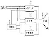
도 4는 도 3에 도시된 바와 같이 스위칭모드 전원공급기를 채용한 디스플레이 장치의 개략적 블럭도를 도시한 것이다.FIG. 4 shows a schematic block diagram of a display device employing a switched mode power supply as shown in FIG. 3.
도 4를 참조하면, 디스플레이장치는 수직동기 및 수평동기신호와 비데오 신호를 입력하는 비디오회로(3)와, 전자빔을 수직 및 수평방향으로 편항시켜 주기 위한 평향회로(4)와, 상기 비디오회로(3) 및 편향회로(4)를 제어하기 위한 마이컴(2)와, 상기 비디오회로(3), 편향회로(4) 및 마이컴(2)에 소정의 전원전압을 인가하기 위한 본 발명의 실시예에 따른 SMPS(1)와, 상기 비디오회로(3)에서 출력되는 비디오신호를 편향회로(4)로의 출력에 의해 디스플레이시켜 주기 위한 CRT(5)로 구성된다.Referring to FIG. 4, the display apparatus includes a
상기 디스플레이장치는 과전압 및 과전류 보호기능을 갖는 스위칭모드 전원공급기의 상기 출력부에서 출력되는 전원전압(VA, VB, VC, VD)이 상기 마이크로 컴퓨터, 비디오회로 및 편향회로에 각각 인가된다.In the display device, power voltages VA, VB, VC, and VD output from the output of the switching mode power supply having overvoltage and overcurrent protection are applied to the microcomputer, the video circuit, and the deflection circuit, respectively.
그러므로, 상기 마이컴(2)은 상기 SMPS(1)로부터 인가되는 전원에 따라 표시수단인 CRT(5)가 각 디스플레이모드 즉, 정상상태, 대기상태, 일시정지상태 및 오프상태에 따라 비디오신호를 디스플레이하도록 상기 비디오회로(3) 및 편향회로(4)를 제어한다.Therefore, the microcomputer 2 displays the video signal according to the display mode, that is, the normal state, the standby state, the pause state, and the off state of the CRT 5, which is a display means according to the power supplied from the SMPS 1 The
디스플레이장치에 있어서, 전원공급을 위하여 종래의 SMPS를 채용하는 경우에는, 부하의 단선 또는 단락과 같은 이상상태발생시 과전류 또는 과전압이 발생되어 회로에 치명적인 영향을 미치게 되었으나, 본 발명의 SMPS를 채용하는 경우에는 부하의 단선 또는 단락과 같은 이상상태발생시 SMPS의 동작을 정지시켜 줌으로써 회로의 손상 등을 미연에 방지할 수 있게 된다.In the display apparatus, when a conventional SMPS is used to supply power, an overcurrent or an overvoltage is generated when an abnormal state such as a disconnection or short circuit of a load occurs, which has a fatal effect on the circuit. However, when the SMPS of the present invention is adopted. In case of abnormal condition such as disconnection or short circuit of load, the operation of SMPS is stopped to prevent damage to circuit.
이상 설명한 바와 같이, 본 발명은 부하에서 과전압이 발생하거나 또는 부하의 단락 등에 기인한 이상상태가 발생되는 경우 회로를 보호할 수 있어 이상전압에 기인한 회로 손상을 효과적으로 방지할 수 있게 된다.As described above, the present invention can protect the circuit when an overvoltage occurs in the load or an abnormal condition caused by a short circuit or the like of the load, thereby effectively preventing circuit damage due to the abnormal voltage.
Claims (1)
Translated fromKoreanPriority Applications (2)
| Application Number | Priority Date | Filing Date | Title |
|---|---|---|---|
| KR1019970005239AKR100229507B1 (en) | 1997-02-21 | 1997-02-21 | Switching mode power supplier having function of protecting circuit from abnormal voltage |
| US09/026,407US5917716A (en) | 1997-02-21 | 1998-02-19 | Switching mode power supplier having function of protecting circuit from abnormal voltage |
Applications Claiming Priority (1)
| Application Number | Priority Date | Filing Date | Title |
|---|---|---|---|
| KR1019970005239AKR100229507B1 (en) | 1997-02-21 | 1997-02-21 | Switching mode power supplier having function of protecting circuit from abnormal voltage |
Publications (2)
| Publication Number | Publication Date |
|---|---|
| KR19980068568A KR19980068568A (en) | 1998-10-26 |
| KR100229507B1true KR100229507B1 (en) | 1999-11-15 |
Family
ID=19497573
Family Applications (1)
| Application Number | Title | Priority Date | Filing Date |
|---|---|---|---|
| KR1019970005239AExpired - Fee RelatedKR100229507B1 (en) | 1997-02-21 | 1997-02-21 | Switching mode power supplier having function of protecting circuit from abnormal voltage |
Country Status (2)
| Country | Link |
|---|---|
| US (1) | US5917716A (en) |
| KR (1) | KR100229507B1 (en) |
Families Citing this family (43)
| Publication number | Priority date | Publication date | Assignee | Title |
|---|---|---|---|---|
| KR100280790B1 (en)* | 1998-07-07 | 2001-02-01 | 윤종용 | Surge protection circuit of display device |
| JP3298624B2 (en)* | 1999-01-19 | 2002-07-02 | 船井電機株式会社 | Switching power supply |
| KR100598412B1 (en)* | 1999-08-31 | 2006-07-10 | 삼성전자주식회사 | Power saving device and power saving method of display system |
| JP2004505359A (en)* | 2000-07-20 | 2004-02-19 | コーニンクレッカ フィリップス エレクトロニクス エヌ ヴィ | Mode switching power supply control |
| KR100387380B1 (en)* | 2000-09-08 | 2003-06-19 | 박준호 | Switching mode power supply with high efficiency |
| US6605931B2 (en) | 2000-11-07 | 2003-08-12 | Microsemi Corporation | Switching regulator with transient recovery circuit |
| US6356063B1 (en) | 2000-11-07 | 2002-03-12 | Linfinity Microelectronics | Switching regulator with transient recovery circuit |
| KR100438695B1 (en)* | 2001-03-09 | 2004-07-05 | 삼성전자주식회사 | Apparatus for controlling power supply and method thereof |
| US6396716B1 (en)* | 2001-09-20 | 2002-05-28 | The University Of Hong Kong | Apparatus for improving stability and dynamic response of half-bridge converter |
| CN1457139A (en)* | 2002-05-08 | 2003-11-19 | 精工爱普生株式会社 | Stabilized voltage swtich supply with overpressure output protective circuit and electronic device |
| KR20040008069A (en)* | 2002-07-15 | 2004-01-28 | 삼성전자주식회사 | Switching mode power supply for lowering stand-by power consumption |
| US6841983B2 (en)* | 2002-11-14 | 2005-01-11 | Fyre Storm, Inc. | Digital signal to pulse converter and method of digital signal to pulse conversion |
| KR101126766B1 (en)* | 2005-02-28 | 2012-04-12 | 페어차일드코리아반도체 주식회사 | Switching mode power supply and method for protection operation thereof |
| KR100692567B1 (en)* | 2005-10-28 | 2007-03-13 | 삼성전자주식회사 | Switching mode power supply and power saving mode |
| CN101212134B (en)* | 2006-12-28 | 2011-05-04 | 华润矽威科技(上海)有限公司 | Over-voltage protection circuit for boosting-type switching power supply |
| TWI330445B (en)* | 2007-01-29 | 2010-09-11 | Chimei Innolux Corp | Power control circuit and liquid crystal display device using the same |
| JP2008218216A (en)* | 2007-03-05 | 2008-09-18 | Sony Corp | Fluorescent tube drive method and device |
| CN101378231B (en)* | 2007-08-31 | 2011-06-15 | 群康科技(深圳)有限公司 | Power supply circuit |
| CN101398548B (en)* | 2007-09-28 | 2010-05-26 | 群康科技(深圳)有限公司 | Electric power circuit and LCD |
| CN101471605B (en)* | 2007-12-29 | 2011-12-07 | 群康科技(深圳)有限公司 | Power supply circuit |
| CN101431233B (en)* | 2008-08-21 | 2012-05-23 | 艾默生网络能源有限公司 | Detection protection circuit of constant power output power supply |
| CN101751881B (en)* | 2008-12-10 | 2012-07-04 | 群康科技(深圳)有限公司 | Liquid crystal display device of external image signal source |
| TWI425757B (en)* | 2009-02-19 | 2014-02-01 | Leadtrend Tech Corp | Power converter and related method |
| CN101964589A (en)* | 2009-07-22 | 2011-02-02 | Bcd半导体制造有限公司 | Method and device for controlling output current of convertor |
| CN102064532B (en)* | 2011-01-12 | 2013-07-03 | 茂硕电源科技股份有限公司 | Overvoltage protection circuit of input follower type |
| JP5712704B2 (en) | 2011-03-14 | 2015-05-07 | 株式会社リコー | High voltage inverter device |
| JP5644810B2 (en)* | 2011-09-26 | 2014-12-24 | 株式会社デンソー | Signal and power transmission equipment |
| CN102611079B (en)* | 2012-03-13 | 2015-01-21 | 华为技术有限公司 | Short-circuit protection system and short-circuit protection method for isolated power converter |
| JP5971074B2 (en)* | 2012-10-15 | 2016-08-17 | 富士電機株式会社 | Switching power supply |
| TW201509103A (en)* | 2013-08-23 | 2015-03-01 | Yottacontrol Co | Switched-mode DC power supply for providing stable voltage output |
| US9831768B2 (en) | 2014-07-17 | 2017-11-28 | Crane Electronics, Inc. | Dynamic maneuvering configuration for multiple control modes in a unified servo system |
| DE102015214165A1 (en)* | 2015-07-27 | 2017-02-02 | Continental Automotive Gmbh | Switching regulator for generating a plurality of DC voltages |
| US9780635B1 (en) | 2016-06-10 | 2017-10-03 | Crane Electronics, Inc. | Dynamic sharing average current mode control for active-reset and self-driven synchronous rectification for power converters |
| TWI630780B (en)* | 2016-07-11 | 2018-07-21 | 萬勝發科技股份有限公司 | Integrated circuit device and setting method thereof |
| US9735566B1 (en) | 2016-12-12 | 2017-08-15 | Crane Electronics, Inc. | Proactively operational over-voltage protection circuit |
| US9742183B1 (en) | 2016-12-09 | 2017-08-22 | Crane Electronics, Inc. | Proactively operational over-voltage protection circuit |
| CN106786354A (en)* | 2017-02-22 | 2017-05-31 | 中领世能(天津)科技有限公司 | Over-pressure safety device and electric power system |
| US11075543B2 (en)* | 2017-04-28 | 2021-07-27 | Samsung Electronics Co., Ltd | Wireless power transmitting device and electronic device for wirelessly receiving power |
| KR102407897B1 (en)* | 2017-04-28 | 2022-06-13 | 삼성전자주식회사 | Wireless power transmitting device and electronic device for wirelessly receiving power |
| JP6930336B2 (en)* | 2017-09-27 | 2021-09-01 | ヤマハ株式会社 | Power supply circuit and audio equipment |
| US9979285B1 (en) | 2017-10-17 | 2018-05-22 | Crane Electronics, Inc. | Radiation tolerant, analog latch peak current mode control for power converters |
| US10425080B1 (en) | 2018-11-06 | 2019-09-24 | Crane Electronics, Inc. | Magnetic peak current mode control for radiation tolerant active driven synchronous power converters |
| JP2022151261A (en)* | 2021-03-26 | 2022-10-07 | セイコーエプソン株式会社 | Power controller and switching power supply |
Family Cites Families (18)
| Publication number | Priority date | Publication date | Assignee | Title |
|---|---|---|---|---|
| US4236187A (en)* | 1977-10-18 | 1980-11-25 | Sharp Kabushiki Kaisha | Power supply voltage stabilizer |
| US4130862A (en)* | 1978-02-01 | 1978-12-19 | Apple Computer, Inc. | DC Power supply |
| US4858052A (en)* | 1986-11-28 | 1989-08-15 | Ro Associates | Method and means for protecting converter circuits |
| DE3840406A1 (en)* | 1987-11-30 | 1989-06-08 | Gold Star Co | Protective circuit for a switched-mode power supply circuit |
| US4876637A (en)* | 1988-03-22 | 1989-10-24 | Kabushiki Kaisha Toshiba | Power converter and method of controlling the same |
| US4916569A (en)* | 1988-11-04 | 1990-04-10 | Zenith Electronics Corporation | Short circuit protection for switch mode power supply |
| US5124906A (en)* | 1990-01-12 | 1992-06-23 | Kang Ki D | Multiple transformer switch mode power supply |
| US5448469A (en)* | 1990-02-15 | 1995-09-05 | Deutsche Thomson-Brandt Gmbh | Switch mode power supply with output feedback isolation |
| US5029269A (en)* | 1990-04-12 | 1991-07-02 | Rockwell International Corporation | Delayed power supply overvoltage shutdown apparatus |
| JPH04150767A (en)* | 1990-10-08 | 1992-05-25 | Fuji Electric Co Ltd | Switching power supply circuit |
| JPH04331461A (en)* | 1991-05-01 | 1992-11-19 | Sony Corp | Switching power supply |
| DE69401965T2 (en)* | 1993-01-21 | 1997-10-09 | Lambda Electronics Inc | Overload protection of a switching power supply |
| JP3349781B2 (en)* | 1993-08-30 | 2002-11-25 | 富士通株式会社 | Switching regulator power supply |
| US5594631A (en)* | 1994-04-20 | 1997-01-14 | The Boeing Company | Digital pulse width modulator for power supply control |
| KR0133633B1 (en)* | 1994-07-21 | 1998-04-23 | 이형도 | Switching mode power supply circuit with output voltage control and overcurrent protection |
| KR0144540B1 (en)* | 1994-08-25 | 1998-10-01 | 김광호 | Surge Protection Circuits in Switched-Mode Power Supplies |
| US5657218A (en)* | 1994-09-07 | 1997-08-12 | Deutsche Thomson Brandt Gmbh | Switch mode power supply circuit |
| US5784231A (en)* | 1997-04-25 | 1998-07-21 | Philips Electronics North America Corp. | Overvoltage protection for SMPS based on demagnetization signal |
- 1997
- 1997-02-21KRKR1019970005239Apatent/KR100229507B1/ennot_activeExpired - Fee Related
- 1998
- 1998-02-19USUS09/026,407patent/US5917716A/ennot_activeExpired - Lifetime
Also Published As
| Publication number | Publication date |
|---|---|
| KR19980068568A (en) | 1998-10-26 |
| US5917716A (en) | 1999-06-29 |
Similar Documents
| Publication | Publication Date | Title |
|---|---|---|
| KR100229507B1 (en) | Switching mode power supplier having function of protecting circuit from abnormal voltage | |
| KR0162847B1 (en) | Switched-Mode Power Supplies with Overcurrent and Overvoltage Protection | |
| KR100296635B1 (en) | Smps having low voltage protection circuit | |
| KR100601640B1 (en) | Power Circuit Protection Device | |
| US20070047274A1 (en) | Power supplying apparatus and power supplying method | |
| US10615681B2 (en) | Switching power supply circuit | |
| KR100291447B1 (en) | Overload Protection of Switching Mode Power Supplies | |
| US20090052212A1 (en) | Power supply apparatus | |
| US20040066662A1 (en) | Power supply device and method having a spark prevention function | |
| KR100369834B1 (en) | Power controlling system and method for display | |
| KR20060130310A (en) | Electronic device and control method | |
| US20060023477A1 (en) | Electronic apparatus | |
| KR100520090B1 (en) | Switching Mode Power Supplies with Overvoltage Protection Circuits | |
| KR100577435B1 (en) | Power Stabilization Circuit of Switching Mode Power Supply | |
| KR100819436B1 (en) | Power factor correction circuit | |
| KR100310204B1 (en) | Circuit for removing residual magnetism of cathode ray tube according to degaussing coil | |
| KR200172696Y1 (en) | Over voltage protection circuit | |
| KR0126331Y1 (en) | Noise Protection Circuit of Multi-Output Switching Power Supply | |
| KR19980038757U (en) | DC power supply with overvoltage protection circuit | |
| KR20000007851A (en) | Switching mode power supply having both power source | |
| KR0122729B1 (en) | Overload detection circuit of power supply | |
| KR19990052751A (en) | DC / DC converter protection circuit of monitor | |
| KR19980042929U (en) | Switching Mode Power Supply Protection Circuit | |
| KR960008170Y1 (en) | T.v. relay-off circuit | |
| KR100895014B1 (en) | Overcurrent Protection Circuit of Ringer Power Supply |
Legal Events
| Date | Code | Title | Description |
|---|---|---|---|
| A201 | Request for examination | ||
| PA0109 | Patent application | St.27 status event code:A-0-1-A10-A12-nap-PA0109 | |
| PA0201 | Request for examination | St.27 status event code:A-1-2-D10-D11-exm-PA0201 | |
| R17-X000 | Change to representative recorded | St.27 status event code:A-3-3-R10-R17-oth-X000 | |
| PG1501 | Laying open of application | St.27 status event code:A-1-1-Q10-Q12-nap-PG1501 | |
| R18-X000 | Changes to party contact information recorded | St.27 status event code:A-3-3-R10-R18-oth-X000 | |
| PN2301 | Change of applicant | St.27 status event code:A-3-3-R10-R13-asn-PN2301 St.27 status event code:A-3-3-R10-R11-asn-PN2301 | |
| E902 | Notification of reason for refusal | ||
| PE0902 | Notice of grounds for rejection | St.27 status event code:A-1-2-D10-D21-exm-PE0902 | |
| T11-X000 | Administrative time limit extension requested | St.27 status event code:U-3-3-T10-T11-oth-X000 | |
| T11-X000 | Administrative time limit extension requested | St.27 status event code:U-3-3-T10-T11-oth-X000 | |
| P11-X000 | Amendment of application requested | St.27 status event code:A-2-2-P10-P11-nap-X000 | |
| P13-X000 | Application amended | St.27 status event code:A-2-2-P10-P13-nap-X000 | |
| T13-X000 | Administrative time limit extension granted | St.27 status event code:U-3-3-T10-T13-oth-X000 | |
| E701 | Decision to grant or registration of patent right | ||
| PE0701 | Decision of registration | St.27 status event code:A-1-2-D10-D22-exm-PE0701 | |
| GRNT | Written decision to grant | ||
| PR0701 | Registration of establishment | St.27 status event code:A-2-4-F10-F11-exm-PR0701 | |
| PR1002 | Payment of registration fee | St.27 status event code:A-2-2-U10-U11-oth-PR1002 Fee payment year number:1 | |
| PN2301 | Change of applicant | St.27 status event code:A-5-5-R10-R13-asn-PN2301 St.27 status event code:A-5-5-R10-R11-asn-PN2301 | |
| PG1601 | Publication of registration | St.27 status event code:A-4-4-Q10-Q13-nap-PG1601 | |
| R18-X000 | Changes to party contact information recorded | St.27 status event code:A-5-5-R10-R18-oth-X000 | |
| PN2301 | Change of applicant | St.27 status event code:A-5-5-R10-R13-asn-PN2301 St.27 status event code:A-5-5-R10-R11-asn-PN2301 | |
| PR1001 | Payment of annual fee | St.27 status event code:A-4-4-U10-U11-oth-PR1001 Fee payment year number:4 | |
| R18-X000 | Changes to party contact information recorded | St.27 status event code:A-5-5-R10-R18-oth-X000 | |
| R18-X000 | Changes to party contact information recorded | St.27 status event code:A-5-5-R10-R18-oth-X000 | |
| PR1001 | Payment of annual fee | St.27 status event code:A-4-4-U10-U11-oth-PR1001 Fee payment year number:5 | |
| R18-X000 | Changes to party contact information recorded | St.27 status event code:A-5-5-R10-R18-oth-X000 | |
| PR1001 | Payment of annual fee | St.27 status event code:A-4-4-U10-U11-oth-PR1001 Fee payment year number:6 | |
| PN2301 | Change of applicant | St.27 status event code:A-5-5-R10-R13-asn-PN2301 St.27 status event code:A-5-5-R10-R11-asn-PN2301 | |
| PR1001 | Payment of annual fee | St.27 status event code:A-4-4-U10-U11-oth-PR1001 Fee payment year number:7 | |
| PN2301 | Change of applicant | St.27 status event code:A-5-5-R10-R13-asn-PN2301 St.27 status event code:A-5-5-R10-R11-asn-PN2301 | |
| PR1001 | Payment of annual fee | St.27 status event code:A-4-4-U10-U11-oth-PR1001 Fee payment year number:8 | |
| PR1001 | Payment of annual fee | St.27 status event code:A-4-4-U10-U11-oth-PR1001 Fee payment year number:9 | |
| PR1001 | Payment of annual fee | St.27 status event code:A-4-4-U10-U11-oth-PR1001 Fee payment year number:10 | |
| PR1001 | Payment of annual fee | St.27 status event code:A-4-4-U10-U11-oth-PR1001 Fee payment year number:11 | |
| PR1001 | Payment of annual fee | St.27 status event code:A-4-4-U10-U11-oth-PR1001 Fee payment year number:12 | |
| PR1001 | Payment of annual fee | St.27 status event code:A-4-4-U10-U11-oth-PR1001 Fee payment year number:13 | |
| R18-X000 | Changes to party contact information recorded | St.27 status event code:A-5-5-R10-R18-oth-X000 | |
| FPAY | Annual fee payment | Payment date:20120730 Year of fee payment:14 | |
| PR1001 | Payment of annual fee | St.27 status event code:A-4-4-U10-U11-oth-PR1001 Fee payment year number:14 | |
| FPAY | Annual fee payment | Payment date:20130730 Year of fee payment:15 | |
| PR1001 | Payment of annual fee | St.27 status event code:A-4-4-U10-U11-oth-PR1001 Fee payment year number:15 | |
| FPAY | Annual fee payment | Payment date:20140730 Year of fee payment:16 | |
| PR1001 | Payment of annual fee | St.27 status event code:A-4-4-U10-U11-oth-PR1001 Fee payment year number:16 | |
| FPAY | Annual fee payment | Payment date:20150730 Year of fee payment:17 | |
| PR1001 | Payment of annual fee | St.27 status event code:A-4-4-U10-U11-oth-PR1001 Fee payment year number:17 | |
| LAPS | Lapse due to unpaid annual fee | ||
| PC1903 | Unpaid annual fee | St.27 status event code:A-4-4-U10-U13-oth-PC1903 Not in force date:20160818 Payment event data comment text:Termination Category : DEFAULT_OF_REGISTRATION_FEE | |
| PC1903 | Unpaid annual fee | St.27 status event code:N-4-6-H10-H13-oth-PC1903 Ip right cessation event data comment text:Termination Category : DEFAULT_OF_REGISTRATION_FEE Not in force date:20160818 |