KR100214917B1 - Semiconductor device and method of manufacturing the same - Google Patents
Semiconductor device and method of manufacturing the sameDownload PDFInfo
- Publication number
- KR100214917B1 KR100214917B1KR1019970000980AKR19970000980AKR100214917B1KR 100214917 B1KR100214917 B1KR 100214917B1KR 1019970000980 AKR1019970000980 AKR 1019970000980AKR 19970000980 AKR19970000980 AKR 19970000980AKR 100214917 B1KR100214917 B1KR 100214917B1
- Authority
- KR
- South Korea
- Prior art keywords
- insulating layer
- semiconductor device
- semiconductor substrate
- manufacturing
- region
- Prior art date
- Legal status (The legal status is an assumption and is not a legal conclusion. Google has not performed a legal analysis and makes no representation as to the accuracy of the status listed.)
- Expired - Fee Related
Links
Images


Classifications
- H—ELECTRICITY
- H01—ELECTRIC ELEMENTS
- H01L—SEMICONDUCTOR DEVICES NOT COVERED BY CLASS H10
- H01L21/00—Processes or apparatus adapted for the manufacture or treatment of semiconductor or solid state devices or of parts thereof
- H01L21/70—Manufacture or treatment of devices consisting of a plurality of solid state components formed in or on a common substrate or of parts thereof; Manufacture of integrated circuit devices or of parts thereof
- H01L21/71—Manufacture of specific parts of devices defined in group H01L21/70
- H01L21/76—Making of isolation regions between components
- H01L21/762—Dielectric regions, e.g. EPIC dielectric isolation, LOCOS; Trench refilling techniques, SOI technology, use of channel stoppers
- H01L21/76224—Dielectric regions, e.g. EPIC dielectric isolation, LOCOS; Trench refilling techniques, SOI technology, use of channel stoppers using trench refilling with dielectric materials
- H01L21/76229—Concurrent filling of a plurality of trenches having a different trench shape or dimension, e.g. rectangular and V-shaped trenches, wide and narrow trenches, shallow and deep trenches
- H—ELECTRICITY
- H10—SEMICONDUCTOR DEVICES; ELECTRIC SOLID-STATE DEVICES NOT OTHERWISE PROVIDED FOR
- H10D—INORGANIC ELECTRIC SEMICONDUCTOR DEVICES
- H10D84/00—Integrated devices formed in or on semiconductor substrates that comprise only semiconducting layers, e.g. on Si wafers or on GaAs-on-Si wafers
Landscapes
- Engineering & Computer Science (AREA)
- Physics & Mathematics (AREA)
- Condensed Matter Physics & Semiconductors (AREA)
- General Physics & Mathematics (AREA)
- Manufacturing & Machinery (AREA)
- Computer Hardware Design (AREA)
- Microelectronics & Electronic Packaging (AREA)
- Power Engineering (AREA)
- Element Separation (AREA)
- Insulated Gate Type Field-Effect Transistor (AREA)
- Semiconductor Memories (AREA)
Abstract
Translated fromKoreanDescription
Translated fromKorean본 발명은 반도체 장치 및 그 제조 방법에 관한 것으로, 특히, 서로 인접한 소자 형성 영역(element formation region)을 전기적으로 분리시키는 소자 분리 영역(element isolating region)을 갖는 반도체 장치 및 그 제조 방법에 관한 것이다.BACKGROUND OF THE
예를 들어, DRAM(Dynamic Random Access Memory)에는 도 41의 메모리 셀 어레이(100a)와, 열 또는 행 디코더(100b)와 같은 주변 회로 영역이 제공된다. 각각의 영역을 전기적으로 분리시키는 소자 분리 영역(100c)은 메모리 셀 어레이(100a)와 주변 회로 영역(예를 들어, 디코더(100b)) 사이에 제공된다. 메모리 셀 어레이와 디코더와 같은 각각의 소자를 접속하는 배선 배치등의 관계로 인해, 소자 분리 영역(100c)에는 소정의 폭 W2가 요구된다.For example, the DRAM (Dynamic Random Access Memory) is provided with the
이와 같은 소자 분리 영역(100c)에는 종래 기술의 LOCOS(Local Oxidation of Silicon) 기법에 의해 소자 분리 산화막(element isolating oxide film)이 배열되며, 이러한 소자 분리 산화막은 각각의 영역을 전기적으로 분리시킨다. 그렇지만, 소자 분리 산화막에는 새 부리(bird's beak) 형상의 부분이 형성되어 그 부분만큼 소자 분리 영역의 크기가 증가되기 때문에 장치의 크기를 줄이는 것이 어렵다. 따라서, 새 부리 형상 부분이 없고, 장치의 크기를 용이하게 줄일 수 있는 분리 방안으로서 트렌치 분리(trench isolation)가 사용되어 왔다. 이러한 트렌치 분리는 기판에 마련된 트렌치내에 절연층(insulating layer)을 채워넣음으로써 이루어진다. 이하, 종래 기술의 트렌치 분리를 갖는 반도체에 관해 기술될 것이다.In this
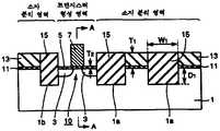
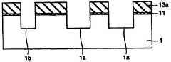
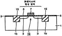
도 42는 종래 기술의 트렌치 분리를 갖는 반도체 장치의 구성을 개략적으로 도시한 도면이다. 도 43은 도 42의 F-F 라인을 따라 취해진 개략 단면도이다.42 is a diagram schematically showing a configuration of a semiconductor device having a trench isolation of the prior art. 43 is a schematic cross sectional view taken along the line F-F in FIG. 42;
도 42 및 도 43을 참조하면, 반도체 기판(1)에는 트렌지스터 형성 영역과, 이 트랜지스터 형성 영역을 다른 소자로부터 전기적으로 분리시키는 소자 분리 영역이 형성되어 있다. 또한, 도 42에서, 트랜지스터 형성 영역 주위에 위치된 영역은 소자 분리 영역이라고 지칭한다.42 and 43, a transistor formation region and an element isolation region for electrically separating the transistor formation region from other elements are formed in the
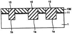
트랜지스터 형성 영역에서, MOS(Metal Oxide Semiconductor) 트랜지스터(10)는 반도체 기판(1)의 주 표면에 형성되어 있다. MOS 트랜지스터(10)는 한쌍의 소스/드레인 영역(3, 3)과, 게이트 절연층(5)과, 게이트 전극층(7)을 포함한다. 한쌍의 소스/드레인 영역(3, 3)은 반도체 기판(1)의 주 표면에 서로 거리를 두고 형성된다. 게이트 전극층(7)은 한쌍의 소스/드레인 영역(3, 3) 사이에 위치되는 영역상의 절연층(5)을 개재하여 형성된다. 또한, 전극층(7)은 다른 소자를 전기적으로 접속하기 위해 소정의 방향으로 연장되고, 소자 분리 영역상으로 또한 연장된다.In the transistor formation region, a metal oxide semiconductor (MOS)
트랜지스터 형성 영역의 도면에서 우측의 소자 분리 영역에는 트렌치(1c)가 제공된다. 트렌치(1c)의 폭 W2은 예를 들어 10㎛보다 큰 폭을 갖는다. 트렌치(1c) 안을 매립하도록 이 트렌치(1c)내에 분리 절연층(15)이 형성된다.The
또한, 트랜지스터 형성 영역의 도면에서 좌측의 소자 분리 영역에는 트렌치(1b)내에 절연층(15)이 매립되는 트랜치 분리가 형성된다.Further, trench isolation in which the
이하, 종래 기술의 트랜치 분리를 갖는 반도체 장치의 제조 방법에 관해 기술될 것이다. 도 44 내지 도 49는 종래 기술의 트랜치 분리를 갖는 반도체 장치의 제조 방법을 공정 순서에 따라 개략적으로 도시한 도면이다. 도 44를 참조하면, 실리콘 산화막(silicon oxide film)으로 이루어진 절연층(11)이 반도체 기판(1)상에 형성되고, 절연층(11)상에는 CVD(Chemical Vapor Deposition) 기법에 의해 200nm 두께의 실리콘 질화막(silicon nitride film)(113)이 형성된다. 포토리쏘그래피(photolithography) 기법에 의해 실리콘 질화막(113)상에는 레지스트 패턴(resist pattern)(133)이 형성된다. 실리콘 질화막(113)과 절연층(11)은 레지스트 패턴(133)을 마스크(mask)로서 사용하여 드라이 에칭(dry etching)을 수행함으로써, 패터닝된다.Hereinafter, a method for manufacturing a semiconductor device having trench isolation of the prior art will be described. 44 to 49 are diagrams schematically showing a manufacturing method of a semiconductor device having a trench isolation according to the prior art according to a process sequence. Referring to FIG. 44, an
이에 따라, 소자 분리 영역 및 트랜지스터 형성 영역을 에워싸는 영역의 반도체 기판(1)의 주 표면이 노출된다. 그후, 래지스트 패턴(133)을 마스크로서 사용한 상태에서 반도체 기판(1)의 노출된 주 표면상에 에칭이 수행된다. 그후, 레지스트 패턴(133)이 제거된다.As a result, the main surface of the
도 45를 참조하면, 전술한 에칭에 의해 반도체 기판(1)의 주 표면 상에 트렌치(1b, 1c)가 200∼400nm의 깊이로 형성된다.Referring to FIG. 45,
도 46을 참조하면, 트렌치(1b, 1c)를 매립하고, 실리콘 질화막(113)상을 덮도록 실리콘 질화막으로 이루어지는 분리 절연층(15)이 CVD 기법에 의해 500nm 두께로 형성된다. 그후, 연마법(polishing method)에 의해 분리 절연층(15)은 적어도 실리콘 질화막(113)의 표면이 노출될 때까지 에칭된다.Referring to FIG. 46, the
도 47을 참조하면, 이러한 에칭이 수행되면, 실리콘 질화막(113)의 표면이 노출되고, 트렌치(1b, 1c)를 매립하도록 분리 절연층(15)이 남게된다. 그후, 분리 절연층(15)에 가볍게 에칭이 더 수행된다.Referring to FIG. 47, when the etching is performed, the surface of the
도 48을 참조하면, 이러한 에칭에 의해 분리 절연층(15)의 막을 감소시킨다. 그 후, 실리콘 질화막(113)은 열 인산(thermal phosphoric acid) 기법에 의해 제거되고, 절연층(11)도 또한 제거된다.Referring to Fig. 48, the etching of the
도 49를 참조하면, 트렌치(1b, 1c)가 분리 절연층(15)으로 매립된 트렌치 분리가 이러한 방식으로 형성된다.Referring to FIG. 49, trench isolation in which
그후, 열 산화법(thermal oxidation method) 또는 CVD 기법에 의해 게이트 절연층(5)이 형성된다. 그후, CVD 기법에 의해 다결정 실리콘 또는 티타늄 실리사이드(titanium silicide)와 같은 금속 실리사이드의 전도성 박막이 300nm의 두께로 형성된 다음 포토리쏘그래피 또는 에칭 기법에 의해 패터닝된다. 그후, 게이트 전극층(7)을 형성한 다음, 이온 주입등의 기법으로 소스/드레인 영역을 형성하면, 도 42 및 도 43에 도시된 반도체 장치가 완성된다.Thereafter, the
종래 기술의 제조 방법에 있어서, 도 46 및 도 47에 도시된 공정의 분리 절연층(15)은 예를 들어 CMP(Chemical Mechanical Polishing) 기법에 의해 연마된다. 이러한 연마는 웨이퍼 표면에 연마포(polishing cloth)를 압착하면서, 화학 기계적으로 수행된다. 이러한 연마포는 연마시 휘어지는 경우가 있다. 따라서, 도 42에 도시된 트렌치(1c)의 폭 W2이 10㎛보다 크면, 연마포의 휘어짐에 따라 분리 절연층(15)의 표면이 오목하게 패인 형상으로 되어 버린다.In the manufacturing method of the prior art, the
이러한 분리 절연층(15) 표면이 오목하게 되면, 그 표면에서 단차가 발생되어 평탄성이 저해되며, 이로 인해 다음과 같은 문제점들이 야기될 수 있다.When the surface of the
(1) 이러한 단차는 렌즈의 높은 NA화와 더불어 의도된 초점 깊이를 보장하기가 어렵다.(1) This step is difficult to guarantee the intended focal depth along with the high NA of the lens.
(2) 이러한 단차는 헐레이션(halation)을 야기시킬 수 있으므로 정밀도 높은 패턴 형성이 어렵다.(2) Since such a step may cause halation, high precision pattern formation is difficult.
(3) 게이트 전극층을 패터닝할 때, 제거되지 않은 게이트 전극층이 남아 있게 되어 각각의 게이트 전극층 사이가 단락될 수 있다.(3) When patterning the gate electrode layer, an unremoved gate electrode layer remains, which may cause a short circuit between the respective gate electrode layers.
또한, 분리 절연층(15)의 표면은 도 42에 도시된 바와 같이 오목한 면을 가지므로, 국부적으로 분리 절연층(15)의 박막 T4가 지극히 작게 된다. 이 경우, 게이트 전극층(7)과 반도체 기판(1) 사이에는 큰 기생 용량(parasitic capacitance)이 발생되는 문제점이 있다.In addition, since the surface of the
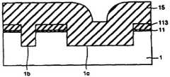
분리 절연층(15)에 단차를 없애는 방법으로서, 도 50에 도시된 구성의 방안이 사용될 수 있다.As a method of eliminating the step in the
도 50을 참조하면, 이 단면도는 도 42의 단면도에 대응하는 도면이다. 또한, 도 50의 G-G 라인을 따라 취해진 단면도는 도 43에 도시된 단면도와 동일하다. 트랜지스터 형성 영역의 도면에서 우측 소자 분리 영역의 트렌치는 10㎛ 이하의 폭 W3을 갖는 다수의 트렌치(1a)로 분할되어 있다. 트렌치(1a)의 폭 W3을 10㎛ 이하로 하면, 분리 절연층(15)의 연마로 인해 표면이 오목해지는 것을 억제할 수 있어 실질적으로 평탄한 표면을 형성할 수 있다. 이로 인해, 전술한 문제점 (1)∼(3)들이 제거될 수 있다.Referring to FIG. 50, this cross sectional view corresponds to the cross sectional view of FIG. 42. In addition, the cross-sectional view taken along the GG line of FIG. 50 is the same as the cross-sectional view shown in FIG. 43. In the figure of the transistor formation region, the trench of the right element isolation region is divided into a plurality of
그러나, 이 경우, 게이트 전극층(7)과 반도체 기판(1) 사이에는 게이트 절연층(5)만이 제공된다. 또한, 게이트 절연층(5)은 MOS 트랜지스터의 특성으로 인해, 예를 들어, 50∼100Å 박막 두께로 형성된다. 이로 인해, 게이트 전극층(7)과 반도체 기판(1)이 서로 대향하는 소자 분리 영역의 영역 R3에서, 게이트 전극층(7)과 반도체 기판(1) 사이에 큰 기생 용량이 발생되는 문제를 해결하지 못한다.In this case, however, only the
또한, 도 50에 도시된 구조는 소위 역 협 채널 효과(reverse narrow channel effect)로 인해 고속 동작이 수행되기 어려운 문제점이 있다. 이하, 이에 대한 설명이 기술될 것이다.In addition, the structure shown in FIG. 50 has a problem that high-speed operation is difficult to perform due to a so-called reverse narrow channel effect. Hereinafter, a description thereof will be described.
도 51은 도 50의 트랜지스터 형성 영역을 확대하여 도시한 개략 단면도이다. 도 51을 참조하면, 게이트 전극층(7)에 전압이 인가되면, 반전에 의해 반도체 기판(1)의 주 표면에 채널(4a)이 형성되고, 소스/드레인 영역(3) 사이에 전류가 흐르게 된다. 또한, 이러한 구조의 영역 R4에서 게이트 전극층(7)과 반도체 기판(1) 사이에 위치되는 분리 절연층(15)의 두께는 비교적 얇다. 따라서, 채널(4a) 이외에, 채널(4b)이 채널(4a)보다 깊은 위치에 트렌치(1b)의 측벽을 따라 형성된다.FIG. 51 is an enlarged schematic cross-sectional view illustrating the transistor formation region of FIG. 50. Referring to FIG. 51, when a voltage is applied to the
채널(4b)이 형성되는 영역은 채널(4a)이 형성되는 영역보다 일반적으로 불순물로 도핑(dope)되는 양이 적다. 따라서, 채널(4b)의 반전 전압은 채널(4a)의 반전 전압보다 높다.The region where the
도 52에 도시된 바와 같이, 게이트 전극에 인가되는 전압(게이트 전압) VG가 전압 V1보다 낮으면, 채널(4a)만이 소스/드레인 영역 사이에 전류가 인가되도록 동작한다. 그러나, 게이트 전압 VG이 전압 V1에 도달하면, 채널(4b)이 반전하여 생성되기 때문에, 채널(4a, 4b)에 의해 소스/드레인 영역 사이에 전류가 인가된다. 따라서, 게이트 전압 VG이 전압 V1에 도달하게 되면, 드레인 전류 ID는 급격하게 상승된다. 이와 같이 드레인 전류가 ID가 급격하게 상승되면, 상승시 펄스 파형이 왜곡되고 고속 동작이 어렵게 된다.As shown in Fig. 52, when the voltage (gate voltage) VG applied to the gate electrode is lower than the voltage V1, only the
따라서, 본 발명의 목적은 게이트 전극의 기생 용량의 증가를 억제하고, 고속 동작을 용이하게 하는 반도체 장치 및 그 제조 방법을 제공하는데 있다.Accordingly, it is an object of the present invention to provide a semiconductor device and a method of manufacturing the same which suppress an increase in parasitic capacitance of a gate electrode and facilitate high speed operation.
본 발명의 반도체 장치는 서로 인접하는 소자 형성 영역을 전기적으로 분리시키는 소자 분리 영역을 갖는 반도체 장치에 있어서 반도체 기판과, 제 1 절연층과, 제 2 절연층과, 전도층을 포함한다. 반도체 기판은 주 표면을 가지며, 소자 분리 영역내의 주 표면에 다수의 트렌치를 제공한다. 제 1 절연층은 트렌치를 매립하고, 주 표면상에서 위쪽으로 돌출된다. 제 1 절연층의 주 표면상에서 위쪽으로 돌출된 부분은 트렌치의 측벽면에 실질적으로 연속하는 측벽면을 갖는다. 제 2 절연층은 다수의 트렌치 사이에 위치되는 주 표면 전면상에 형성되고, 제 1 절연층과 상이한 재료로 형성된다. 전도층은 소자 형성 영역내의 소자와 전기적으로 접속되고, 소자 형성 영역내에서 주 표면상에 제 3 절연층을 개재하여 형성되어 있으며, 소자 분리 영역내에서 제 1 및 제 2 절연층의 상부 표면상으로 연장한다. 제 2 절연층의 두께는 제 3 절연층의 두께보다 크다.A semiconductor device of the present invention includes a semiconductor substrate, a first insulating layer, a second insulating layer, and a conductive layer in a semiconductor device having element isolation regions electrically separating the element formation regions adjacent to each other. The semiconductor substrate has a major surface and provides a plurality of trenches in the major surface in the device isolation region. The first insulating layer fills the trench and protrudes upward on the major surface. The upwardly protruding portion on the major surface of the first insulating layer has a sidewall surface that is substantially continuous with the sidewall surface of the trench. The second insulating layer is formed on the major surface front surface located between the plurality of trenches, and is formed of a material different from the first insulating layer. The conductive layer is electrically connected to the element in the element formation region, and is formed on the main surface in the element formation region via a third insulating layer, and on the upper surface of the first and second insulation layers in the element isolation region. To extend. The thickness of the second insulating layer is greater than the thickness of the third insulating layer.
본 발명의 반도체 장치에서, 소자 분리 영역의 제 2 절연층은 소자 형성 영역의 제 3 절연층보다 큰 막두께를 갖는다. 따라서, 전도층과 반도체 기판 사이에 위치하는 절연층의 두께는 소자 형성 영역보다 소자 분리 영역 쪽이 크다. 따라서, 소자 분리 영역의 전도층과 반도체 기판 사이의 기생 용량은 종래 기술보다 적다.In the semiconductor device of the present invention, the second insulating layer of the element isolation region has a larger film thickness than the third insulating layer of the element formation region. Therefore, the thickness of the insulating layer located between the conductive layer and the semiconductor substrate is larger in the device isolation region than in the device formation region. Thus, the parasitic capacitance between the conductive layer in the device isolation region and the semiconductor substrate is less than in the prior art.
소자 분리 영역의 트렌치를 매립하는 제 1 절연층은 주 표면에서 윗쪽으로 돌출되고, 돌출된 부분에 있어서 트렌치의 측벽면과 실질적으로 연속하는 측벽면을 갖는다. 따라서, 절연층이 단지 트렌치만을 매립하는 종래의 예에 비해 제 1 절연층상에 위치되는 전도층과 반도체 기판의 간극을 크게 확보할 수 있다. 따라서, 전도층이 게이트 전극층인 경우, 채널은 소자 형성 영역의 표면 영역에만 형성될 수 있다. 따라서, 드레인 전류가 급격하게 증가되지 않게 되고, 상승시 펄스 파형이 왜곡되지 않으므로 고속 동작이 용이하게 수행된다.The first insulating layer filling the trench in the device isolation region protrudes upward from the major surface and has a sidewall surface that is substantially continuous with the sidewall surface of the trench in the protruding portion. Therefore, as compared with the conventional example in which the insulating layer only fills the trench, it is possible to secure a large gap between the conductive layer and the semiconductor substrate located on the first insulating layer. Thus, when the conductive layer is a gate electrode layer, the channel can be formed only in the surface region of the element formation region. Therefore, the drain current does not increase rapidly, and since the pulse waveform is not distorted at the time of rise, high-speed operation is easily performed.
또한, 소자 분리 영역내에서 트렌치가 다수로 분할되어 있기 때문에, 각각의 트렌치의 폭은 적절한 값으로 설정될 수 있다. 따라서, 예를 들어, 연마시 트렌치의 폭이 너무 넓어지므로 트렌치를 매립하는 절연층의 상부 표면이 오목 형상으로 변경되는 것이 방지된다. 따라서, 오목 형상에 의한 단차가 발생되지 않기 때문에, 트렌치상에서 패터닝이 정확하게 수행된다.In addition, since the trench is divided into a plurality in the device isolation region, the width of each trench can be set to an appropriate value. Thus, for example, the width of the trench becomes too wide during polishing, so that the upper surface of the insulating layer filling the trench is prevented from changing into a concave shape. Therefore, since no step due to the concave shape occurs, patterning is accurately performed on the trench.
본 발명의 하나의 특성에 따른 반도체 장치의 제조 방법은 다음과 같은 공정을 포함한다. 먼저, 반도체 기판의 주 표면상에 제 1 및 제 2 절연층을 순차적으로 형성한 후, 제 1 및 제 2 절연층을 사전설정된 형태로 패터닝한다. 그후, 패터닝된 제 1 및 제 2 절연층을 마스크(mask)로서 사용하여 반도체 기판의 주 표면에 에칭을 수행함으로써, 소자 분리 영역내에 다수의 트렌치를 형성한다. 이어서, 트렌치를 매립하고 제 2 절연층을 덮도록, 제 1 절연층과 상이한 재료로 이루어진 제 3 절연층을 형성한다. 이어서, 제 2 절연층의 상부 표면이 적어도 노출될 때까지 제 3 절연층을 연마하여 제거함으로써, 제 2 및 제 3 절연층의 상부 표면이 실질적으로 동일한 평면으로 형성되도록 한다. 그후, 제 1 및 제 3 절연층의 상부 표면이 실질적으로 동일한 표면으로 형성되도록 제 3 절연층을 제거한다. 그후, 제 2 절연층을 제거한다. 이어서, 제 3 절연층의 제거는 어렵고 제 1 절연층의 제거는 용이한 조건에서 에칭을 수행함으로써, 소자 형성 영역내의 제 1 절연층을 선택적으로 제거한다. 이어서, 소자 형성 영역내의 반도체 기판의 주 표면상에 제 4 절연층을 개재하여 전도층을 형성한다.A method for manufacturing a semiconductor device according to one aspect of the present invention includes the following steps. First, the first and second insulating layers are sequentially formed on the main surface of the semiconductor substrate, and then the first and second insulating layers are patterned in a predetermined form. Thereafter, etching is performed on the major surface of the semiconductor substrate using the patterned first and second insulating layers as masks, thereby forming a plurality of trenches in the device isolation region. Next, a third insulating layer made of a material different from the first insulating layer is formed so as to fill the trench and cover the second insulating layer. The third insulating layer is then polished and removed until at least the top surface of the second insulating layer is exposed so that the top surfaces of the second and third insulating layers are formed in substantially the same plane. Thereafter, the third insulating layer is removed so that the upper surfaces of the first and third insulating layers are formed to be substantially the same surface. Thereafter, the second insulating layer is removed. Subsequently, the removal of the third insulating layer is difficult and the removal of the first insulating layer is performed by etching under easy conditions, thereby selectively removing the first insulating layer in the element formation region. Next, a conductive layer is formed on the main surface of the semiconductor substrate in the element formation region via the fourth insulating layer.
본 발명의 다른 특성에 따른 반도체 장치의 제조 방법은 다음과 같은 공정을 포함한다.A method for manufacturing a semiconductor device according to another aspect of the present invention includes the following steps.
반도체 기판의 주 표면상에 제 1 절연층을 형성한 후, 제 1 절연층을 사전설정된 형태로 패터닝한다. 그후, 패터닝된 제 1 절연층을 마스크로서 사용하여 반도체 기판의 주 표면에 에칭을 수행함으로써, 소자 분리 영역내에 다수의 트렌치를 형성한다. 이어서, 트렌치를 매립하고 제 1 절연층상을 덮도록 제 1 절연층과 상이한 재료로 이루어진 제 2 절연층을 형성한다. 그후, 제 1 절연층의 상부 표면이 적어도 노출될 때까지 제 2 절연층을 연마하여 제거함으로써, 제 1 및 제 2 절연층의 상부 표면이 실질적으로 동일한 평면으로 형성되도록 한다. 이어서, 제 2 절연층의 제거는 어렵고 제 1 절연층의 제거는 용이한 조건에서 에칭을 수행함으로써, 소자 형성 영역내의 제 1 절연층을 선택적으로 제거한다. 이어서, 소자 형성 영역내의 반도체 기판의 주 표면상에 제 3 절연층을 개재하여 전도층을 형성한다.After forming the first insulating layer on the main surface of the semiconductor substrate, the first insulating layer is patterned into a predetermined form. Thereafter, etching is performed on the main surface of the semiconductor substrate using the patterned first insulating layer as a mask, thereby forming a plurality of trenches in the device isolation region. Subsequently, a second insulating layer made of a material different from the first insulating layer is formed so as to fill the trench and cover the first insulating layer. The second insulating layer is then polished and removed until at least the top surface of the first insulating layer is exposed so that the top surfaces of the first and second insulating layers are formed in substantially the same plane. Subsequently, etching of the second insulating layer is difficult and removal of the first insulating layer is easily performed, thereby selectively removing the first insulating layer in the element formation region. Next, a conductive layer is formed on the main surface of the semiconductor substrate in the element formation region via the third insulating layer.
전술한 2개의 특성을 갖는 반도체 장치의 제조 방법에 따르면, 전도층과 반도체 기판 사이의 기생 용량을 줄일 수 있고, 고속 동작을 용이하게 수행하고, 패터닝이 정확한 반도체 장치가 제조될 수 있다.According to the method for manufacturing a semiconductor device having the two characteristics described above, a parasitic capacitance between the conductive layer and the semiconductor substrate can be reduced, a high speed operation can be easily performed, and a semiconductor device with accurate patterning can be manufactured.
도 1은 본 발명의 제 1 실시예의 반도체 장치의 구성을 개략적으로 도시한 단면도.1 is a cross-sectional view schematically showing the configuration of a semiconductor device of a first embodiment of the present invention.
도 2는 도 1의 A-A 라인을 따라 취해진 개략 단면도.2 is a schematic cross-sectional view taken along the line A-A of FIG.
도 3은 본 발명의 제 1 실시예의 반도체 장치의 제조 방법의 제 1 공정을 개략적으로 도시한 단면도.Fig. 3 is a sectional view schematically showing a first step of the manufacturing method of the semiconductor device of the first embodiment of the present invention.
도 4는 본 발명의 제 1 실시예의 반도체 장치의 제조 방법의 제 2 공정을 개략적으로 도시한 단면도.4 is a cross-sectional view schematically showing a second step of the manufacturing method of the semiconductor device of the first embodiment of the present invention.
도 5는 본 발명의 제 1 실시예의 반도체 장치의 제조 방법의 제 3 공정을 개략적으로 도시한 단면도.Fig. 5 is a sectional view schematically showing the third process of the method of manufacturing the semiconductor device of the first embodiment of the present invention.
도 6은 본 발명의 제 1 실시예의 반도체 장치의 제조 방법의 제 4 공정을 개략적으로 도시한 단면도.Fig. 6 is a sectional view schematically showing a fourth step of the method of manufacturing the semiconductor device of the first embodiment of the present invention.
도 7은 본 발명의 제 1 실시예의 반도체 제조 장치의 제조 방법의 제 5 공정을 개략적으로 도시한 단면도.Fig. 7 is a sectional view schematically showing a fifth step of the manufacturing method of the semiconductor manufacturing apparatus of the first embodiment of the present invention.
도 8은 본 발명의 제 1 실시예의 반도체 장치의 제조 방법의 제 6 공정을 개략적으로 도시한 단면도.Fig. 8 is a cross-sectional view schematically showing the sixth step of the manufacturing method of the semiconductor device of the first embodiment of the present invention.
도 9는 본 발명의 제 1 실시예의 반도체 장치의 제조 방법의 제 7 공정을 개략적으로 도시한 단면도.9 is a sectional views schematically showing a seventh step of the method of manufacturing a semiconductor device of the first embodiment of the present invention.
도 10은 본 발명의 제 1 실시예의 반도체 장치의 제조 방법의 제 8 공정을 개략적으로 도시한 단면도.Fig. 10 is a sectional view schematically showing an eighth step of the manufacturing method of the semiconductor device of the first embodiment of the present invention.
도 11은 본 발명의 제 2 실시예의 반도체 장치의 구성을 개략적으로 도시한 단면도.Fig. 11 is a sectional view schematically showing the structure of a semiconductor device of a second embodiment of the present invention.
도 12는 도 11의 B-B 라인을 따라 취해진 개략 단면도.12 is a schematic cross sectional view taken along the line B-B in FIG.
도 13은 본 발명의 제 2 실시예의 반도체 장치의 제조 방법의 제 1 공정을 개략적으로 도시한 단면도.Fig. 13 is a sectional view schematically showing a first step of the manufacturing method of the semiconductor device of the second embodiment of the present invention.
도 14는 본 발명의 제 2 실시예의 반도체 장치의 제조 방법의 제 2 공정을 개략적으로 도시한 단면도.Fig. 14 is a sectional view schematically showing a second step of the manufacturing method of the semiconductor device of the second embodiment of the present invention.
도 15는 본 발명의 제 2 실시예의 반도체 장치의 제조 방법의 제 3 공정을 개략적으로 도시한 단면도.Fig. 15 is a sectional view schematically showing the third process of the method of manufacturing the semiconductor device of the second embodiment of the present invention.
도 16은 본 발명의 제 3 실시예의 반도체 장치의 구성을 개략적으로 도시한 단면도.Fig. 16 is a sectional view schematically showing the structure of a semiconductor device of a third embodiment of the present invention.
도 17은 도 16의 C-C 라인을 따라 취해진 개략 단면도.FIG. 17 is a schematic cross sectional view taken along line C-C in FIG. 16; FIG.
도 18은 본 발명의 제 3 실시예의 반도체 장치의 제조 방법의 제 1 공정을 개략적으로 도시한 단면도.Fig. 18 is a sectional view schematically showing a first step of the manufacturing method of the semiconductor device of the third embodiment of the present invention.
도 19는 본 발명의 제 3 실시예의 반도체 장치의 제조 방법의 제 2 공정을 개략적으로 도시한 단면도.Fig. 19 is a sectional view schematically showing a second step of the manufacturing method of the semiconductor device of the third embodiment of the present invention.
도 20은 본 발명의 제 3 실시예의 반도체 장치의 제조 방법의 제 3 공정을 개략적으로 도시한 단면도.20 is a sectional views schematically showing a third process of the method of manufacturing the semiconductor device of the third embodiment of the present invention.
도 21은 본 발명의 제 3 실시예의 반도체 장치의 제조 방법의 제 4 공정을 개략적으로 도시한 단면도.Fig. 21 is a sectional view schematically showing a fourth step of the method for manufacturing the semiconductor device of the third embodiment of the present invention.
도 22는 본 발명의 제 3 실시예의 반도체 장치의 제조 방법의 제 5 공정을 개략적으로 도시한 단면도.Fig. 22 is a sectional views schematically showing a fifth step of the manufacturing method of the semiconductor device of the third embodiment of the invention.
도 23은 본 발명의 제 3 실시예의 반도체 장치의 제조 방법의 제 6 공정을 개략적으로 도시한 단면도.Fig. 23 is a sectional view schematically showing a sixth step of the method of manufacturing a semiconductor device of the third embodiment of the present invention.
도 24는 본 발명의 제 4 실시예의 반도체 장치의 제조 방법의 제 1 공정을 개략적으로 도시한 단면도.Fig. 24 is a sectional view schematically showing a first step of the manufacturing method of the semiconductor device of the fourth embodiment of the present invention.
도 25는 본 발명의 제 4 실시예의 반도체 장치의 제조 방법의 제 2 공정을 개략적으로 도시한 단면도.Fig. 25 is a sectional view schematically showing a second step of the manufacturing method of the semiconductor device of the fourth embodiment of the present invention.
도 26은 본 발명의 제 4 실시예의 반도체 장치의 제조 방법의 제 3 공정을 개략적으로 도시한 단면도.Fig. 26 is a cross-sectional view schematically showing a third step of the manufacturing method of the semiconductor device of the fourth embodiment of the invention.
도 27은 본 발명의 제 4 실시예의 반도체 장치의 제조 방법의 제 4 공정을 개략적으로 도시한 단면도.Fig. 27 is a sectional view schematically showing a fourth step of the method for manufacturing the semiconductor device of the fourth embodiment of the present invention.
도 28은 본 발명의 제 4 실시예의 반도체 장치의 제조 방법의 제 5 공정을 개략적으로 도시한 단면도.Fig. 28 is a sectional views schematically showing a fifth step of the manufacturing method of the semiconductor device of the fourth embodiment of the present invention.
도 29는 본 발명의 제 5 실시예의 반도체 장치의 제조 방법의 제 1 공정을 개략적으로 도시한 단면도.Fig. 29 is a sectional view schematically showing a first step of the manufacturing method of the semiconductor device of the fifth embodiment of the present invention.
도 30은 본 발명의 제 5 실시예의 반도체 장치의 제조 방법의 제 2 공정을 개략적으로 도시한 단면도.Fig. 30 is a sectional view schematically showing a second step of the manufacturing method of the semiconductor device of the fifth embodiment of the present invention.
도 31은 본 발명의 제 5 실시예의 반도체 장치의 제조 방법의 제 3 공정을 개략적으로 도시한 단면도.Fig. 31 is a sectional view schematically showing a third step of the manufacturing method of the semiconductor device of the fifth embodiment of the present invention.
도 32는 본 발명의 제 5 실시예의 반도체 장치의 제조 방법의 제 4 공정을 개략적으로 도시한 단면도.32 is a cross-sectional view schematically showing a fourth step of the manufacturing method of the semiconductor device of the fifth embodiment of the present invention.
도 33은 본 발명의 제 5 실시예의 반도체 장치의 제조 방법의 제 5 공정을 개략적으로 도시한 단면도.33 is a sectional views schematically showing a fifth step of the manufacturing method of the semiconductor device of the fifth embodiment of the present invention.
도 34는 본 발명의 제 5 실시예의 반도체 장치의 제조 방법의 제 6 공정을 개략적으로 도시한 단면도.34 is a sectional views schematically showing a sixth step of the manufacturing method of the semiconductor device of the fifth embodiment of the present invention.
도 35는 본 발명의 제 6 실시예의 반도체 장치의 제조 방법의 제 1 공정을 개략적으로 도시한 단면도.Fig. 35 is a sectional view schematically showing the first step of the manufacturing method of the semiconductor device of the sixth embodiment of the present invention.
도 36은 본 발명의 제 6 실시예의 반도체 장치의 제조 방법의 제 2 공정을 개략적으로 도시한 단면도.Fig. 36 is a sectional view schematically showing a second step of the manufacturing method of the semiconductor device of the sixth embodiment of the present invention.
도 37은 본 발명의 제 6 실시예의 반도체 장치의 제조 방법의 제 3 공정을 개략적으로 도시한 단면도.37 is a sectional views schematically showing a third step of the manufacturing method of the semiconductor device of the sixth embodiment of the present invention.
도 38은 2개 이상의 트렌치를 갖는 소자 분리 영역에 의해 에워싸인 트랜지스터 형성 영역을 개략적으로 도시한 평면도.FIG. 38 is a plan view schematically showing a transistor formation region surrounded by an isolation region with two or more trenches; FIG.
도 39는 도 38의 D-D 라인을 따라 취해진 개략 단면도.FIG. 39 is a schematic cross sectional view taken along the line D-D in FIG. 38;
도 40은 도 38의 E-E 라인을 따라 취해진 개략 단면도.40 is a schematic cross sectional view taken along the E-E line in FIG. 38;
도 41은 DRAM에서 메모리 셀 어레이 및 디코드와 같은 주변 회로 영역의 평면 계층상의 간극을 개략적으로 도시한 도면.FIG. 41 is a schematic illustration of the gap on a planar hierarchy of peripheral circuit areas such as memory cell arrays and decodes in DRAM.
도 42는 종래의 반도체 장치의 구성을 개략적으로 도시한 단면도.42 is a sectional views schematically showing a structure of a conventional semiconductor device.
도 43은 도 42의 F-F 라인을 따라 취해진 개략 단면도.FIG. 43 is a schematic cross sectional view taken along the line F-F in FIG. 42;
도 44는 종래의 반도체 장치의 제조 방법의 제 1 공정을 개략적으로 도시한 단면도.44 is a sectional views schematically showing a first step of the method of manufacturing a conventional semiconductor device.
도 45는 종래의 반도체 장치의 제조 방법의 제 2 공정을 개략적으로 도시한 단면도.45 is a sectional views schematically showing a second step of the method of manufacturing a conventional semiconductor device.
도 46은 종래의 반도체 장치의 제조 방법의 제 3 공정을 개략적으로 도시한 단면도.46 is a sectional views schematically showing a third process of the method of manufacturing a conventional semiconductor device.
도 47은 종래의 반도체 장치의 제조 방법의 제 4 공정을 개략적으로 도시한 단면도.47 is a sectional views schematically showing a fourth step of the method of manufacturing a conventional semiconductor device.
도 48는 종래의 반도체 장치의 제조 방법의 제 5 공정을 개략적으로 도시한 단면도.48 is a sectional views schematically showing a fifth step of the method of manufacturing a conventional semiconductor device.
도 49는 종래의 반도체 장치의 제조 방법의 제 6 공정을 개략적으로 도시한 단면도.49 is a sectional views schematically showing a sixth step of the method of manufacturing a conventional semiconductor device.
도 50은 소자 분리 영역에 2개 이상의 트렌치를 서로 분리시켜 마련한 구성을 개략적으로 도시한 단면도.50 is a cross-sectional view schematically showing a configuration in which two or more trenches are separated from each other in an element isolation region;
도 51은 도 50에 도시된 구성에서 채널의 생성을 도시한 개략 단면도.FIG. 51 is a schematic sectional view showing generation of a channel in the configuration shown in FIG. 50; FIG.
도 52는 도 50에 도시된 구조에서 게이트 전압과 드레인 전류간의 관계를 도시한 그래프.FIG. 52 is a graph showing a relationship between a gate voltage and a drain current in the structure shown in FIG. 50; FIG.
도면의 주요 부분에 대한 부호의 설명Explanation of symbols for the main parts of the drawings
1: 반도체 기판1a, 1b: 트렌치1:
3: 소스/드레인 영역5: 게이트 절연층3: source / drain region 5: gate insulating layer
7: 게이트 전극층11, 13a, 13b, 13d: 절연층7:
15: 분리 절연층7a: 제 1 전도층15:
7b: 제 2 전도층7c: 전도층7b: second
이하, 본 발명의 실시예는 도면을 기초하여 기술될 것이다.Hereinafter, embodiments of the present invention will be described based on the drawings.
제 1 실시예First embodiment
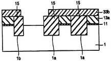
도 1은 본 발명의 제 1 실시예에 따른 반도체 장치의 구성을 개략적으로 도시한 단면도이다. 또한, 도 2는 도 1의 A-A 라인을 따라 취해진 개략 단면도이다.1 is a cross-sectional view schematically showing a configuration of a semiconductor device according to a first embodiment of the present invention. 2 is a schematic cross-sectional view taken along the A-A line of FIG. 1.
도 1 및 도 2를 참조하면, 본 실시예의 반도체 장치는 트랜지스터 형성 영역과, 트랜지스터를 다른 소자로부터 전기적으로 분리시키는 소자 분리 영역을 갖는다. 도 1에서, 트랜지스터 형성 영역의 주위에 위치된 영역은 소자 분리 영역으로 칭한다.1 and 2, the semiconductor device of this embodiment has a transistor formation region and an element isolation region for electrically separating the transistor from other elements. In Fig. 1, the region located around the transistor formation region is called an element isolation region.
트랜지스터 형성 영역에서, MOS 트랜지스터(10)는 반도체 기판(1)의 주 표면에 형성되고, 한쌍의 소스/드레인 영역(3, 3)과, 게이트 절연층(5)과, 게이트 전극층(7)을 포함한다. 한쌍의 소스/드레인 영역(3)은 반도체 기판(1)의 주 표면과 서로 거리를 두고 형성된다. 게이트 전극층(7)은 한쌍의 소스/드레인 영역(3, 3) 사이에 위치되는 영역상에 게이트 절연층(5)을 개재하여 형성된다.In the transistor formation region, the
소자 분리 영역에는 트렌치 분리 구조가 이용된다. 트렌치 분리 구조는 트렌치(1a, 1b) 및 분리 절연층(15)을 포함한다.A trench isolation structure is used for the device isolation region. The trench isolation structure includes
소자 분리 영역에는 2개 이상의 트렌치(1a)가 형성된다. 또한, 소자 분리 영역에는 적어도 하나의 트렌치(1b)가 형성된다. 분리 절연층(15)은 트렌치(1a, 1b)를 매립하고, 반도체 기판(1)의 주 표면에서 윗쪽으로 돌출되도록 형성된다. 분리 절연층(15)의 반도체 기판(1)의 주 표면에서 윗쪽으로 돌출된 부분의 측벽면은 트렌치(1a, 1b)의 측벽면과 연속한다. 또한, 트렌치(1a, 1a) 사이에 위치되는 반도체 기판(1)의 주 표면상에는 절연층(11) 및 절연층(13)이 분리 절연층(15)의 측벽에 접하도록 서로 적층하여 형성된다. 또한, 절연층(11) 및 절연층(13)은 트렌치(1b)를 매립하는 분리 절연층(15)에 인접한 위치에도 서로 적층하여 형성된다. 절연층(13)과 분리 절연층(15)은 반도체 기판(1)의 주 표면으로부터 실질적으로 동일한 높이로 위치되고, 실질적으로 동일한 평면을 구성하는 상부 표면을 갖는다.Two or
또한, 트랜지스터 형성 영역내에 게이트 전극층(7)의 상부 표면의 반도체 기판(1)의 주 표면으로부터의 높이는 절연층(13) 및 분리 절연층(15)의 상부 표면의 반도체 기판(1)의 주 표면으로부터의 높이보다 높다. 게이트 전극층(7)은 불순물이 도입된 다결정 실리콘 박막으로 구성되며, 700nm의 두께를 갖는다.In addition, the height from the main surface of the
절연층(11) 및 절연층(13)의 두께의 합 T1은 2000Å 내지 8000Å 범위를 갖는다. 또한, 트렌치(1a)는 0.1㎛ 내지 10㎛의 폭 W1을 가지며, 이 폭W1으로 사전설정된 방향으로 연장한다. 두개의 트렌치(1a, 1b) 사이의 영역은 10㎛ 이하의 폭을 갖는다. 또한, 각각의 트렌지(1a, 1b)의 깊이는 200㎛ 내지 400㎛의 범위를 갖는다.The sum T1 of the thicknesses of the insulating
절연층(5, 11)은 예를 들어, 열 산화 기법 또는 CVD 기법에 의해 형성된 실리콘 산화막으로 형성된다. 절연층(13)은 예를 들어, 인(phosphorus) 또는 붕소(bornon)중 적어도 어느 하나를 포함하는 실리콘 산화막(PSG 막 또는 BPSG 막 등)으로 형성된다. 분리 절연층(15)은 예를 들어, 불순물이 실질적으로 주입되지 않은 실리콘 산화막으로 형성된다.The insulating
이하, 본 실시예의 반도체 장치의 제조 방법에 관해 기술될 것이다.Hereinafter, the manufacturing method of the semiconductor device of this embodiment will be described.
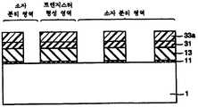
도 3 내지 도 10은 본 발명의 제 1 실시예의 반도체 장치의 제조 방법을 공정 순서에 따라 도시한 개략 단면도이다. 도 3을 참조하면, 열 산화법 또는 CVD 기법에 의해, 반도체 기판(1)의 주 표면에는, 예를 들어, 실리콘 산화막으로 이루어진 절연층(11)이 20nm의 두께로 형성된다. 예를 들어, CVD 기법에 의해 절연층(11)상에는 인 및 붕소 중 적어도 어느 하나를 포함하는 실리콘 산화막(PSG 막 또는 BPSG 막)으로 이루어진 절연층(13)이 500nm의 두께로 형성된다. 예를 들어, CVD 기법에 의해 절연층(13)상에는 실리콘 산화막으로 이루어진 절연층(31)이 100nm의 두께로 형성된다. 포토리쏘그래피 기법에 의해 절연층(31)상에는 레지스트 패턴(33a)이 사전설정된 형태로 형성된다. 레지스트 패턴(33a)은 트랜지스터 형성 영역을 한정하고, 넓은 소자 분리 영역이 10㎛ 이하의 폭을 제각기 갖는 다수의 영역으로 분리되도록 형성된다.3 to 10 are schematic cross-sectional views showing a method for manufacturing a semiconductor device of a first embodiment of the present invention according to a process sequence. Referring to Fig. 3, by thermal oxidation or CVD, an insulating
레지스트 패턴(33a)을 마스크로서 사용함으로써, 드라이 에칭(dry etching) 기법에 의해 반도체 기판(1)의 주 표면이 노출될 때까지 절연층(31, 13, 11)에 순차적으로 에칭이 수행된다.By using the resist
절연층(11)은 절연층(13) 중에서 인 또는 붕소들의 불순물이 반도체 기판(1)에 확산되지 않도록 하는 역할을 한다.The insulating
레지스트 패턴(33a)을 마스크로서 사용한 상태에서, 노출된 반도체 기판(1)의 주 표면에 에칭이 수행된다. 그후, 레지스트 패턴(33a)은 예를 들어, 애싱(ashing)에 의해 제거된다.In the state where the resist
도 4를 참조하면, 전술한 반도체 기판(1)의 에칭에 의해 반도체 기판(1)의 주 표면에 200nm 내지 400nm 범위의 깊이를 선택적으로 갖는 트렌치(1a, 1b)가 형성된다.Referring to FIG. 4, the above described etching of the
트렌치(1a, 1b)를 형성하기 위한 에칭은 레지스트 패턴(33a)을 남긴 상태에서 행하였지만, 이러한 에칭은 레지스트 패턴(33a)을 제거한 후 절연층(31)을 마스크로서 사용하여 실행하여도 좋다.Although the etching for forming the
도 5를 참조하면, 트렌치(1a, 1b)를 매립하고 절연층(31)을 덮도록 예를 들어, 실질적으로 불순물이 포함되지 않은 실리콘 산화막으로 형성된 절연층(15)은 절연층(11, 13, 15)의 두께의 합 이상의 막 두께, 예를 들어, 700nm의 두께 T3으로 형성된다. 그후, 예를 들어, CMP 기법 등의 연마법에 의해 절연층(15)은 적어도 절연층(31)의 표면이 노출될 때까지 연마 제거된다.Referring to FIG. 5, the insulating
도 6을 참조하면, 이러한 연마로 인해 트렌치(1a, 1b)를 매립하는 절연층(15)의 일부만이 남게 되고, 분리 절연층(15) 및 절연층(31)은 실질적으로 서로 동일한 평면을 갖는 상부 표면이 형성된다.Referring to FIG. 6, this polishing leaves only a part of the insulating
연마시에 있어서, 절연층(31)은 스토퍼(stopper)의 역할을 한다. 절연층(31)이 예를 들어 실리콘 질화막으로 형성되고, 절연층(15)이 예를 들어 실리콘 산화막으로 형성되는 경우, 실리콘 질화막은 실리콘 산화막보다 연마되기 어렵다. 따라서, 연마 속도는 절연층(31)의 표면이 노출된 시점에서 감소되므로, 연마 종점이 검출될 수 있다.In polishing, the insulating
절연층(15)의 연마량을 스토퍼없이 충분히 제어할 수 있는 경우에, 절연층(31)은 생략되어도 좋다.In the case where the polishing amount of the insulating
그후, 분리 절연층(15)은 플루오르화산(hydrofluoric acid: HF)으로 드라이 에칭 또는 에칭에 의해 약간 에칭된다.Thereafter, the
도 7을 참조하면, 이러한 에칭으로 인해 분리 절연층(15)의 두께가 감소되며, 이로 인해 분리 절연층(15)과 절연층(13)의 상부 표면이 실질적으로 동일한 평면으로 형성된다. 그후, 절연층(31)은 열 인산에 의해 제거된다.Referring to FIG. 7, the etching reduces the thickness of the
도 8을 참조하면, 절연층(31)이 제거되면, 절연층(13)의 상부 표면이 노출된다. 그러면, 포토리쏘그래피 기법에 의해 홀 패턴(hole pattern)(33b1)을 갖는 레지스트 패턴(33b)이 형성된다. 홀 패턴(33b1)은 적어도 트랜지스터 형성 영역의 절연층(13)의 표면을 노출시킨다. 홀 패턴(33b1)의 개구의 크기는 포토리쏘그래피의 배열 정밀도를 고려하여, 트랜지스터 형성 영역에서 배열 정밀도 크기만큼 크게 설정된다.Referring to FIG. 8, when the insulating
레지스트 패턴(33b)을 마스크로서 사용함으로써, 절연층(13)과 분리 절연층(15) 상에 에칭이 수행된다. 이러한 에칭은 예를 들어, HF 증기(vapor) 기법에 의해 수행된다. 이러한 조건에서는 분리 절연층(15)이 거의 에칭되지 않지만, 절연층(13)만이 선택적으로 에칭된다. 이로 인해, 트랜지스터 형성 영역의 박막 절연층(11)이 노출된다. 그후, 박막 절연층(11)은 희불산 용액으로 에칭 제거된다.By using the resist
절연층(11)이 에칭되면, 분리 절연층(15)도 다소 에칭되지만, 에칭되는 양이 작기 때문에 이러한 에칭된 상태는 도면에 도시되어 있지 않다.When the insulating
도 9를 참조하면, 트랜지스터 형성 영역의 반도체 기판(1)의 주 표면은 박막 절연층(11)을 에칭함으로써 노출된다.Referring to FIG. 9, the main surface of the
전술한 공정을 통해, 트렌치 분리에 따른 소자 분리 구조가 완성된다.Through the above-described process, the device isolation structure according to the trench isolation is completed.
도 10을 참조하면, 열 산화법 또는 CVD 기법에 의해 트랜지스터 형성 영역의 반도체 기판(1)의 주 표면에는 실리콘 산화막(5)이 5nm의 두께로 형성된다. 그후, CVD 기법에 의해, 예를 들어, 불순물이 도입된 다결정 실리콘 막으로 이루어진 전도층(7)이 700nm의 두께로 형성된다.Referring to FIG. 10, a
그후, 전도층(7)은 포토리쏘그래피 기법 및 에칭 기법에 의해 패터닝되어, 도 1 및 도 2에 도시된 바와 같은 게이트 전극층(7)이 형성된다. 그후, 게이트 전극층(7)을 마스크로서 사용하여, 트랜지스터 형성 영역의 반도체 기판(1)의 주 표면에 불순물을 이온 주입함으로써, 이로 인해 한쌍의 소스/드레인 영역(3, 3)이 형성된다. 이러한 방식으로, MOS 트랜지스터(10)가 완성된다.The
상술한 바와 같이, 도 50에 도시된 종래예에서는, 게이트 전극층(7)과 반도체 기판(1) 사이에 위치되는 절연층(5)의 두께는 트랜지스터 형성 영역과 소자 분리 영역 양쪽이 동일하다.As described above, in the conventional example shown in FIG. 50, the thickness of the insulating
이와 대조적으로, 본 실시예의 반도체 장치에서는 도 1에 도시된 소자 분리 영역의 절연층(11 및 13)의 막 두께의 합 T1이 트랜지스터 형성 영역의 게이트 절연층의 두께 T2보다 크게되도록 설정되어 있다. 따라서, 게이트 전극층(7)이 소자 분리 영역내의 절연층(13) 및 분리 절연층(15)상을 연장할 수 있더라도, 소자 분리 영역의 게이트 전극층(7)과 반도체 기판(1) 사이에 위치되는 절연층의 막두께는 트랜지스터 형성 영역의 막 두께보다 크다. 따라서, 게이트 전극층(7)과 반도체 기판(1) 사이의 기생 용량은 종래 기술보다 적게할 수 있다.In contrast, in the semiconductor device of this embodiment, the sum T1 of the film thicknesses of the insulating
분리 절연층(15)은 트렌치(1a, 1b)만을 매립하는 것 뿐만 아니라 반도체 기판(1)의 주 표면상으로 돌출된다. 따라서, 도 50에 도시된 종래 기술의 분리 절연층(15)이 단지 트렌치(1a, 1b)만을 매립하는 구조에 비해, 도 2에 도시된 영역 R1의 게이트 전극층(7)과 반도체 기판(1) 사이의 간격을 크게 확보할 수 있다. 따라서, 트랜지스터 형성 영역의 표면 영역에만 채널을 형성시킬 수 있다. 이로 인해, 드레인 전류는 급격하게 증가되지 않게 되고, 상승시 펄스의 파동이 왜곡되지 않으므로, 고속 동작이 용이하게 수행된다.The
소자 분리 영역내에서는, 트렌치(1a)가 다수로 분할되어 있기 때문에, 각 트렌치(1a)의 폭 W1은 적절한 값(10㎛ 이하)으로 설정될 수 있다. 따라서, 도 5 및 도 6에 도시된 연마시에 있어서 연마포가 휘어지더라도, 분리 절연층(15)의 상부 표면은 오목한 형태로 되지 않는다. 따라서, 오목 상태에 의한 단차가 발생되지 않으므로, 게이트 전극층(7)은 트렌치(1a)상에서 용이하게 패터닝될 수 있다.In the device isolation region, since the
절연층(13)의 상부 표면과 분리 절연층(15)의 상부 표면은 실질적으로 동일한 평면으로 구성되어 있다. 따라서, 절연층(13)과 분리 절연층(15)상에서 예를 들어, 게이트 전극층(7)이 정확하게 패터닝될 수 있다.The upper surface of the insulating
본 실시예의 반도체 장치의 제조 방법에서, 도 8의 분리 절연층(15) 및 절연층(13)은 에칭 속도가 상이한 재료로 형성된다. 따라서, 도 8 및 도 9에 도시된 공정에서, 트랜지스터 형성 영역의 절연층(13)을 제거하는 경우, 분리 절연층(15)의 일부 표면이 레지스트 패턴(33b)으로부터 노출되어 있더라도, 분리 절연층(15)은 거의 제거되지 않으며, 절연층(13)만이 선택적으로 제거될 수 있다.In the manufacturing method of the semiconductor device of this embodiment, the
도 5 및 도 6에 도시된 연마 공정에서는 반도체 기판(1)의 주 표면이 노출되지 않기 때문에, 연마에 의해 반도체 기판(1)의 주 표면이 손상되는 일은 없다. 따라서, MOS 트랜지스터는 신뢰성을 저하시키지 않고 반도체 기판(1)상에 형성될 수 있다.Since the main surface of the
본 실시예에서, 도 10에 도시된 바와 같이, 게이트 전극층(7)의 패터닝은 단차를 갖는 영역 R2의 분리 절연층(15)상에서 수행할 필요가 있다. 이를 고려하여, 이하 단차를 갖는 영역상에서의 에칭을 피할 수 있는 반도체 장치의 구성 및 그 제조 방법이 제 2 실시예로서 기술될 것이다.In this embodiment, as shown in Fig. 10, the patterning of the
제 2 실시예Second embodiment
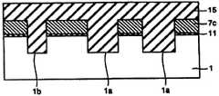
도 11은 본 발명의 제 2 실시예의 반도체 장치의 구성을 개략적으로 도시한 도면이다. 도 12는 도 11의 B-B 라인을 따라 취해진 개략 단면도이다. 도 11 및 도 12를 참조하면, 이 실시예의 구성은 제 1 실시예의 구성과 비교해 볼 때 특히 게이트 전극층의 구성이 상이하다.FIG. 11 is a diagram schematically showing a configuration of a semiconductor device of a second embodiment of the present invention. FIG. 12 is a schematic cross-sectional view taken along the line B-B in FIG. 11 and 12, the configuration of this embodiment is different from the configuration of the gate electrode layer especially when compared with the configuration of the first embodiment.
이 실시예에서, 게이트 전극층은 제 1 전도층(7a) 및 제 2 전도층(7b)의 제 2 층 구조로 형성된다. 제 1 전도층(7a)은 분리 절연층(15) 및 절연층(13)의 상부 표면과 실질적으로 동일한 높이로 형성된 상부 표면을 갖는다. 제 2 전도층(7b)은 제 1 전도층(7a)의 상부 표면에 접하고, 트렌치 분리 구조상에 연장되도록 형성된다.In this embodiment, the gate electrode layer is formed in the second layer structure of the first
제 1 전도층(7a)과 분리 절연층(15) 사이의 영역은 예를 들어, 실리콘 산화막으로 형성된 절연층(21)에 의해 매립된다. 절연층(21)의 상부 표면은 분리 절연층(15) 및 절연층(13)의 상부 표면과 동일한 높이로 형성된다.The region between the first
이외의 구성은 제 1 실시예의 구성과 동일하므로, 동일한 부재는 동일한 참조 부호를 부여하고, 이에 관한 설명은 생략한다.Since the other configurations are the same as the configurations of the first embodiment, the same members are given the same reference numerals, and description thereof will be omitted.
이하, 본 실시예의 제조 방법에 관해 기술될 것이다.Hereinafter, the manufacturing method of this embodiment will be described.
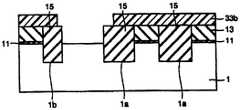
도 13 내지 도 15는 본 발명의 제 2 실시예의 반도체 장치의 제조 방법을 공정 순서에 따라 도시한 개략 단면도이다. 본 실시예의 제조 방법은 도 3 내지 도 10에 도시된 제 1 실시예와 동일한 공정을 거친다. 도 10에 도시된 전도층(7)은 예를 들어 연마법에 의해 분리 절연층(15) 및 절연층(13)의 상부 표면이 노출될 때까지 연마 제거된다.13 to 15 are schematic cross-sectional views showing a method for manufacturing a semiconductor device of a second embodiment of the present invention according to a process sequence. The manufacturing method of this embodiment goes through the same process as the first embodiment shown in Figs. The
도 13을 참조하면, 연마된 전도층(7a)은 분리 절연층(15) 및 절연층(13)의 상부 표면과 실질적으로 동일한 평면을 형성하는 상부 표면을 갖는다. 그후, 전도층(7a)은 포토리쏘그래피 및 에칭 기법에 의해 패터닝된다.Referring to FIG. 13, the polished
도 14를 참조하면, 이러한 패터닝으로 인해 게이트 전극층을 구성하는 제 1 전도층(7a)이 형성된다. 그후, 제 1 전도층(7a)을 마스크로하여 반도체 기판(1)의 주 표면에 불순물을 이온 주입함으로써, 한쌍의 소스/드레인 영역(3)이 형성된다.Referring to FIG. 14, the patterning forms a first
도 15를 참조하면, 예를 들어, CVD 기법에 의해 실리콘 산화막으로 형성되는 절연층(21)은 500nm의 두께로 전체 표면상에 형성된다. 절연층(21)이 에칭백(etchback) 또는 연마법으로 제 1 전도층(7a), 분리 절연층(15) 및 절연층(13)의 상부 표면이 노출될 때까지 연마 제거된다. 그러면, 절연층(21)은 제 1 전도층(7a) 및 분리 절연층(15) 사이에 매립되며, 층 상부 표면과 실질적으로 동일한 높이의 상부 표면을 갖게 된다. 그후, 예를 들어, 금속 실리사이드층(7b)은 CVD등의 기법에 의해 형성되고, 포토리쏘그래피 및 에칭에 의해 패터닝된다. 그러면, 도 11 및 도 12에 도시된 제 2의 전도층(7b)은 제 1 전도층(7a)과 전기적으로 접속되도록, 트렌치 분리 구조상으로 연장되도록 형성된다.Referring to Fig. 15, for example, an insulating
전술한 제조 방법에서는 분리 절연층(15)에 의한 단차부 상에 게이트 전극층이 패터닝될 필요는 없다. 따라서, 게이트 전극층(7a, 7b)이 정확하게 패터닝될 수 있다.In the above-described manufacturing method, the gate electrode layer does not need to be patterned on the stepped portion by the
제 3 실시예Third embodiment
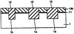
도 16은 본 발명의 제 3 실시예의 반도체 장치의 구성을 개략적으로 도시한 단면도이다. 도 17은 도 16의 C-C의 라인을 따라 취해진 개략 단면도이다.16 is a cross-sectional view schematically showing the configuration of a semiconductor device of a third embodiment of the present invention. 17 is a schematic cross-sectional view taken along the line C-C of FIG. 16.
도 16 및 도 17을 참조하면, 이 실시예의 반도체 장치의 구성은 도 1 및 도 2에 도시된 제 1 실시예의 구성과 비교해 볼 때 절연층(13a)의 재질이 서로 상이하다. 즉, 이 실시예에서, 절연층(13a)은 예를 들어 실리콘 질화막으로 형성된다.16 and 17, the structure of the semiconductor device of this embodiment is different from each other in the material of the insulating
이외의 구성에 대해서는 제 1 실시예의 구성과 동일하므로, 동일한 부재는 동일한 참조 부호를 부여하고, 이에 관한 설명은 생략한다.Since other configurations are the same as those in the first embodiment, the same members are given the same reference numerals and description thereof will be omitted.
이하, 본 실시예의 반도체 장치의 제조 방법에 관해 기술될 것이다.Hereinafter, the manufacturing method of the semiconductor device of this embodiment will be described.
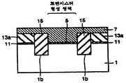
도 18 내지 도 23은 본 발명의 제 3 실시예의 반도체 장치의 제조 방법을 공정 순서에 따라 도시한 개략 단면도이다. 도 18을 참조하면, 반도체 기판(1)의 주 표면상에는 예를 들어, 열 산화법 또는 CVD 기법에 의해 실리콘 산화막으로 이루어진 절연층(11)이 20nm의 두께로 형성된다. 절연층(11)상에는 예를 들어, CVD 기법에 의해 실리콘 질화막으로 이루어진 절연층(13a)이 500nm의 두께로 형성된다. 절연층(13a)상에는 포토리쏘그래피 기법에 의해 레지스트 패턴(33a)이 사전설정된 형태로 형성된다. 그후, 레지스트 패턴(33a)을 마스크로서 사용하여, 절연층(13a, 11)에 순차적으로 에칭하는 드라이 에칭 기법이 수행된다. 그러면, 반도체 기판(1)의 주 표면은 부분적으로 노출된다.18 to 23 are schematic cross-sectional views showing a method for manufacturing a semiconductor device of a third embodiment of the present invention according to a process sequence. Referring to Fig. 18, on the main surface of the
그후, 레지스트 패턴(33a)을 마스크로서 사용한 상태에서, 노출된 반도체 기판(1)의 주 표면에서 에칭이 수행된다. 그후, 레지스트 패턴(33a)이 예를 들어 애싱에 의해 제거된다.Thereafter, in the state where the resist
도 19를 참조하면, 전술한 에칭에 의해 반도체 기판(1)의 주 표면에는 예를 들어, 200∼400nm의 깊이로 트렌치(1a, 1b)가 형성된다.Referring to FIG. 19,
도 20을 참조하면, 예를 들어 CVD 기법에 의해, 실리콘 산화막으로 형성되는 분리 절연층(15)은 트렌치(1a, 1b)를 매립하고, 절연층(13a)을 덮도록 형성된다. 분리 절연층(15)의 두께는 절연층(11, 13a)과 트렌치(1a)의 두께의 합 이상으로 된다.Referring to FIG. 20, for example, by a CVD technique, the
이어서, 분리 절연층(15)은 절연층(13a)의 상부 표면이 적어도 노출될 때까지 연마법 또는 에칭 기법에 의해 연마 또는 에칭된다.Subsequently, the
도 21을 참조하면, 이러한 연마 또는 에칭에 의해 트렌치(1a, 1b)가 매립되고, 절연층(13a)의 상부 표면과 동일한 높이의 상부 표면을 갖는 분리 절연층(15)이 형성된다.Referring to FIG. 21, the
이러한 연마 또는 에칭시 절연층(13a)은 스토퍼로서 작용한다.In such polishing or etching, the insulating
도 22를 참조하면, 포토리쏘그래피에 의해 레지스트 패턴(33b)은 트랜지스터 형성 영역에 위치한 절연층(13a)의 상부 표면이 적어도 노출되는 홀 패턴(33b1)을 갖도록 형성된다. 또한, 홀 패턴(33b1)은 제 1 실시예에서 기술된 것과 동일한 개구 크기를 갖도록 형성된다.Referring to FIG. 22, the resist
레지스트 패턴(33b)을 마스크로서 사용하여 드라이 에칭함으로써, 트랜지스터 형성 영역의 절연층(13a)이 선택적으로 제거된다. 이러한 드라이 에칭에서는 CHF3와 H2의 혼합 가스가 사용된다. 여기서, H2의 분압을 조정함으로써, 실리콘 산화막과 실리콘 질화막의 에칭의 선택비를 임의로 설정할 수 있다. 에칭에 의해 트랜지스터 형성 영역의 절연층(11)이 또한 제거된다. 그후, 레지스트 패턴(33b)이 예를 들어, 애싱(ashing)에 의해 제거된다.By dry etching using the resist
도 23을 참조하면, 절연층(11)의 에칭에 의해 트랜지스터 형성 영역의 반도체 기판(1)의 주 표면이 노출된다. 그후, 도 10에 도시된 제 1 실시예와 마찬가지의 공정을 거쳐, 도 16 및 도 17에 도시된 반도체 장치가 완성된다.Referring to FIG. 23, the main surface of the
전술한 본 실시예의 제조 방법에서는 도 16, 도 17에서 분리 절연층(15)이 실리콘 산화막으로 형성되고 절연층(13a)이 실리콘 질화막으로 형성되는 경우에 대해 설명하였다. 그렇지만, 분리 절연층(15)은 실리콘 질화막으로 형성되어도 좋고, 절연층(13a)은 실리콘 산화막으로 형성되어도 좋다. 이 경우, 도 22 및 도 23에 도시된 절연층(13a)의 에칭에서는 CHF3와 H2의 가스 혼합중 H2의 분압을 조정함으로써, 전술한 경우와는 대조적으로, 실리콘 산화막의 에칭 속도를 실리콘 질화막의 에칭 속도보다 빠르게 할 수 있다. 또한, 혼합 가스대신 HF 수용액을 사용하여 에칭이 수행되는 경우에도, 실리콘 산화막의 에칭 속도가 실리콘 질화막의 에칭 속도보다 빠르게 된다.In the above-described manufacturing method of this embodiment, the
드라이 에칭을 사용하는 경우, 실리콘 산화막을 마스크로서 사용하여 실리콘 산화막을 에칭하는 것은 실리콘 산화막을 마스크로서 사용하여 실리콘 질화막을 에칭하는 경우보다 에칭의 선택비를 크게 설정할 수 있다. 따라서, 드라이 에칭이 사용되는 경우, 분리 절연층(15)은 실리콘 질화막으로 형성되고, 절연층(13a)는 실리콘 산화막으로 형성되는 것이 바람직하다.In the case of using dry etching, etching the silicon oxide film using the silicon oxide film as a mask can set the etching selectivity larger than when etching the silicon nitride film using the silicon oxide film as a mask. Therefore, when dry etching is used, the
한편, 도 20 및 도 21에 도시된 연마 공정에서, 실리콘 질화막의 연마 속도는 실리콘 산화막의 속도보다 늦다. 따라서, 연마를 고려하는 경우, 분리 절연층(15)은 실리콘 산화막으로 형성되고, 절연층(13a)은 실리콘 산화막으로 형성되는 것이 바람직하다.On the other hand, in the polishing process shown in Figs. 20 and 21, the polishing rate of the silicon nitride film is slower than that of the silicon oxide film. Therefore, in consideration of polishing, it is preferable that the
제 4 실시예Fourth embodiment
전술한 제 3 실시예에서, 절연층(13a)은 실리콘 산화막보다 큰 유전 상수(dielectric constant)를 갖는 실리콘 질화막으로 형성된다. 따라서, 제 3 실시예의 게이트 전극층(7)의 기생 용량은 제 1 실시예보다 증대되어 버린다. 이러한 문제점을 해결하는 수단으로서, 실리콘 질화막이 인 또는 붕소들중 적어도 어느 하나가 도핑된 실리콘 산화막으로 대체하여 사용되는 본 실시예가 바람직하다. 이하, 본 실시예의 반도체 장치의 제조 방법에 관해 기술될 것이다.In the third embodiment described above, the insulating
도 24 내지 도 28은 본 발명의 제 4 실시예의 반도체 장치의 제조 방법을 공정 순서에 따라 도시한 개략 단면도이다. 본 실시예의 제조 방법은 도 18 내지 도 21에 도시된 제 3 실시예의 공정과 마찬가지의 공정을 거친다. 그후, 도 21에 도시된 실리콘 질화막으로 형성된 절연층(13a)은 열 인산에 의해 선택적으로 제거된다.24 to 28 are schematic cross-sectional views showing a method for manufacturing a semiconductor device of a fourth embodiment of the present invention according to a process sequence. The manufacturing method of this embodiment goes through the same process as that of the third embodiment shown in Figs. Thereafter, the insulating
이로 인해, 도 24에 도시된 바와 같이 실리콘 산화막으로 형성된 절연층(11)의 표면이 노출된다.As a result, as shown in FIG. 24, the surface of the insulating
도 25를 참조하면, 예를 들어 CVD 기법에 의해 인 또는 붕소 중 적어도 어느 하나가 도핑된 실리콘 산화막이 700nm의 두께로 전체 표면상에 형성된다. 분리 절연층(15)의 상부 표면이 적어도 노출될 때까지, 실리콘 산화막은 예를 들어, 연마법 또는 에칭 기법에 의해 연마 또는 에칭된다. 그러면, 인 또는 붕소 중 적어도 어느 하나가 도핑된 실리콘 산화막으로 형성되는 절연층(13b)의 상부 표면은 분리 절연층(15)의 상부 표면과 실질적으로 동일한 높이를 갖는다.Referring to Fig. 25, a silicon oxide film doped with at least either phosphorus or boron, for example, by CVD is formed on the entire surface at a thickness of 700 nm. The silicon oxide film is polished or etched by, for example, a polishing method or an etching technique until at least the top surface of the
도 26을 참조하면, 포토리쏘그래피에 의해 레지스트 패턴(33b)은 도 8에 도시된 공정과 동일하게 형성된다. 레지스터 패턴(33b)을 마스크로서 사용하여, 트랜지스터 형성 영역의 절연층(13b)에서 에칭이 HF 증기에 의해 수행된다.Referring to FIG. 26, the resist
도 27을 참조하면, 이러한 에칭에 의해 트랜지스터 형성 영역의 절연층(13b)만이 선택적으로 제거되어, 절연층(11)의 표면이 노출된다. 그후, 에칭에 의해 절연층(11)이 제거된다.Referring to FIG. 27, only the insulating
이러한 방식에 의해 트랜지스터 형성 영역의 반도체 기판(1)의 주 표면이 노출된다. 그후, 레지스트 패턴(33b)은 예를 들어, 에싱 기법에 의해 제거되어, 도 28에 도시된 상태로 된다. 이 상태에서 제 1 실시예와 마찬가지로 게이트 절연층과 게이트 전극층이 형성된다.In this manner, the main surface of the
이 실시예에서, 절연층(13b)은 인 또는 붕소 중 적어도 어느 하나가 도핑되는 실리콘 산화막이 이용된다. 따라서, 절연층(13b)이 실리콘 질화막이 이용되는 경우보다 게이트 전극층(7)의 기생 용량을 줄일 수 있다.In this embodiment, a silicon oxide film doped with at least either phosphorus or boron is used for the insulating
제 5 실시예Fifth Embodiment
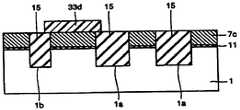
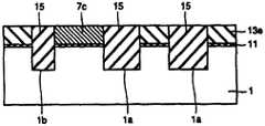
제 3 실시예에서는 도 18에 도시된 절연층(13a)이 실리콘 산화막으로 형성되지만, CVD 기법에 의해 형성된 다결정 실리콘층 또는 비정질 실리콘층(amorphous silicon layer)이 실리콘 질화막대신 사용되어도 좋다. 이하, 다결정 실리콘 또는 비정질 실리콘으로 형성된 절연층(13a)을 포함하는 실시예가 기술될 것이다.In the third embodiment, the insulating
도 29 내지 도 34는 본 발명의 제 5 실시예의 반도체 장치의 제조 방법을 공정 순서에 따라 도시한 개략 단면도이다. 도 29를 참조하면, 반도체 기판(1)의 주 표면상에는 예를 들어, 열 산화법 또는 CVD 기법에 의해 실리콘 산화막으로 이루어진 절연층(11)이 10nm의 두께로 형성된다. 절연층(11)상에는 예를 들어, CVD 기법에 의해 다결정 실리콘막으로 이루어진 전도층(7c)이 400nm 두께로 형성된다. 전도층(7c)은 다결정 실리콘막대신 비정질 실리콘으로 형성되어도 좋다.29 to 34 are schematic cross-sectional views showing the manufacturing method of the semiconductor device of the fifth embodiment of the present invention in the order of steps. Referring to Fig. 29, on the main surface of the
전도층(7c)상에는 포토리쏘그래피에 의해 사전설정된 형태를 갖는 레지스트 패턴(33a)이 형성된다. 레지스트 패턴(33a)을 마스크로서 사용하여, 전도층(7c) 및 절연층(11)은 반도체 기판(1)의 일부 주 표면이 노출되도록 순차적으로 에칭된다. 또한, 노출된 반도체 기판(1)의 주 표면에는 레지스트 패턴(33a)을 마스크로 한 상태에서 에칭이 수행된다. 그후, 레지스트 패턴(33a)은 예를 들어, 애싱 기법에 의해 제거된다.On the
도 30을 참조하면, 이러한 에칭에 의해 반도체 기판(1)의 주 표면에는 200∼400nm 깊이를 갖는 트렌치(1a, 1b)가 형성된다.Referring to FIG. 30,
도 31을 참조하면, 트렌치(1a, 1b)를 매립하고, 전도층(7c)상을 덮도록 실리콘 산화막으로 이루어진 절연층(15)이 예를 들어, 800nm의 두께로 형성된다. 그후, 절연층(15)은 연마법 또는 에칭 기법에 의해 전도층(7c)의 상부 표면이 노출될 때까지 연마 또는 에칭된다.Referring to FIG. 31,
도 32를 참조하면, 전술한 방식에 의해 트렌치(1a, 1b)를 매립하여 전도층(7c)의 상부 표면과 실질적으로 동일한 상부 표면을 갖는 분리 절연층(15)이 형성된다. 그후, 드라이 에칭 기법에 의해 전도층(7c)이 제거된다.Referring to FIG. 32, the
도 33을 참조하면, 전술한 드라이 에칭 기법에 의해 절연층(11)의 표면이 노출된다.Referring to FIG. 33, the surface of the insulating
도 34를 참조하면, 절연층(11) 및 분리 절연층(15)을 덮도록, 예를 들어, 붕소 또는 인 중 적어도 어느 하나를 포함하는 실리콘 산화막(예를 들어, PSG 막, BPSG 막)으로 이루어진 절연층(13d)이 600nm의 두께로 형성된다. 그후, 절연층(13d)는 연마법에 의해 분리 절연층(15)의 상부 표면이 노출될 때까지 연마된다. 그러면, 절연층(13d)의 상부 표면은 분리 절연층(15)의 상부 표면과 실질적으로 동일한 높이로 된다.Referring to FIG. 34, a silicon oxide film (eg, a PSG film or a BPSG film) including at least one of, for example, boron or phosphorus, may be covered to cover the insulating
그후, 도 25 내지 도 28에 도시된 제 4 실시예와 동일한 공정을 수행함으로써 MOS 트랜지스터가 형성되고 반도체 장치가 완성된다.Thereafter, the MOS transistor is formed and the semiconductor device is completed by performing the same process as the fourth embodiment shown in FIGS. 25 to 28.
이 실시예는 전술한 제 4 실시예와 동일한 효과를 갖는다.This embodiment has the same effect as the fourth embodiment described above.
제 6 실시예Sixth embodiment
제 5 실시예서는 도 32 및 도 33에 도시된 다결정 실리콘으로 이루어진 전도층(7c)이 모두 제거된다. 그러나, 전도층(7c)의 일부가 게이트 전극으로서 남겨질 수 있다. 이하, 전도층 일부를 게이트 전극으로서 잔류시키는 방안이 기술될 것이다.In the fifth embodiment, all of the
도 35 내지 도 37은 본 발명의 제 6 실시예의 반도체 장치의 제조 방법을 공정 순서로 도시한 개략 단면도이다. 이 실시예의 제조 방법은 도 29 내지 도 32에 도시된 제 5 실시예와 동일한 공정으로 수행된다. 그후, 도 35를 참조하면, 포토리쏘그래피에 의해 트랜지스터 형성 영역의 전도층(7c)상에만 레지스트 패턴(33d)이 형성된다. 레지스트 패턴(33d)을 마스크로서 사용한 상태에서 전도층(7c)상의 드라이 에칭이 수행된다.35 to 37 are schematic cross-sectional views showing the semiconductor device manufacturing method of the sixth embodiment of the present invention in the order of processes. The manufacturing method of this embodiment is carried out in the same process as the fifth embodiment shown in Figs. Then, referring to FIG. 35, the resist
도 36을 참조하면, 이러한 드라이 에칭에 의해 트랜지스터 형성 영역 이외의 전도층(7c)이 제거되고, 절연층(11)의 표면이 노출된다. 그후, 레지스트 패턴(33d)이 제거된다.Referring to FIG. 36, the
도 37을 참조하면, 붕소 또는 인 중 적어도 어느 하나를 포함하는 실리콘 산화막(예를 들어, PSG 막과 BPSG 막)으로 이루어진 절연층(13e)은 600nm의 두께로 형성된다. 그후, 연마법에 의해 분리 절연층(15)의 상부 표면이 노출될 때까지 절연층(13e)이 연마된다. 그러면, 트랜지스터 형성 영역 이외의 절연층(11)상에는 분리 절연층(15) 및 전도층(7c)의 상부 표면과 실질적으로 동일한 높이를 갖는 절연층(13e)이 남게 된다.Referring to FIG. 37, an insulating layer 13e made of a silicon oxide film (eg, a PSG film and a BPSG film) containing at least one of boron or phosphorus is formed to a thickness of 600 nm. Thereafter, the insulating layer 13e is polished until the upper surface of the
이때, 절연층(13e)은 불순물을 실질적으로 포함하지 않은 실리콘 산화막으로 형성될 수 있다. 그러나, 연마법을 사용하여 매립하는 경우, BPSG 막의 연마 속도는 불순물을 포함하지 않은 실리콘 산화막보다 수배 내지 10배 정도 빠르다. 따라서, BPSG 막 등으로 형성된 절연층(13e)이 사용되면, 분리 절연층(15)의 두께가 감소되는 것이 억제되며, 이로 인해 매립이 더욱 효과적으로 수행될 수 있다.In this case, the insulating layer 13e may be formed of a silicon oxide film substantially free of impurities. However, when buried using the polishing method, the polishing rate of the BPSG film is several times to ten times faster than the silicon oxide film containing no impurities. Therefore, when the insulating layer 13e formed of the BPSG film or the like is used, the thickness of the
그후, 전도층(7c)이 게이트 전극층으로서 사용될 수 있도록 도 14 및 도 15에 도시된 제 2 실시예와 동일한 공정으로 수행된다.Thereafter, the
이 실시예의 제조 방법은 전도층(7c)을 모두 제거한 후에 새로운 전극층을 형성할 필요가 없기 때문에, 제 5 실시예보다 제조 공정을 상당히 줄일 수 있다.Since the manufacturing method of this embodiment does not need to form a new electrode layer after removing all the
이 실시예에서, 전도층(7c)은 비정질 실리콘 또는 TiSi2등과 같은 금속 실리사이드로 형성되거나, 혹은 이들을 조합하여 적층된 막으로 형성될 수 있다. 전도층(7c)은 TiN과 같은 금속 질화막과 금속 실리사이드로 이루어진 적층형 막으로 형성될 수 있다. 이들 막은 도 36의 공정에서 다결정 실리콘과 마찬가지로, 염소(chlorine)에 의해 드라이 에칭될 수 있으므로, 실리콘 산화막으로 이루어진 절연층(15)상에서 에칭이 선택적으로 수행될 수 있다.In this embodiment, the
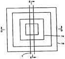
전술한 제 1 내지 제 6 실시예에서, 트랜지스터 형성 영역은 도 38 내지 도 40에 도시된 바와 같이, 2개 이상의 트렌치를 갖는 소자 분리 영역에 둘러싸여 있어도 좋다.In the above-described first to sixth embodiments, the transistor formation region may be surrounded by the device isolation region having two or more trenches, as shown in FIGS. 38 to 40.
도 38은 2개 이상의 트렌치를 갖는 소자 분리 영역에 둘러싸인 트랜지스터 형성 영역을 개략적으로 도시한 도면이다. 도 39 및 도 40은 제각기 도 38의 D-D 라인 및 E-E 라인을 따라 취해진 개략 단면도이다.FIG. 38 schematically illustrates a transistor formation region surrounded by an isolation region having two or more trenches. 39 and 40 are schematic cross sectional views taken along the D-D and E-E lines of FIG. 38, respectively.
지금까지 열거한 실시예는 여러 특징으로 예시한 것으로 이로 한정되지 않음에 유의하여야 한다. 본 발명의 범위는 전술한 설명이 아닌 특허 청구범위에 기술되어 있으며, 특허 청구범위내에서 여러가지 변경이 포함될 수 있음에 유의하여야 한다.It should be noted that the embodiments listed so far are illustrated with various features and not limited thereto. It is noted that the scope of the present invention is set forth in the claims rather than the foregoing description, and various changes may be included within the claims.
본 발명의 반도체 장치에서 소자 분리 영역의 제 2 절연층은 소자 형성 영역의 제 3 절연층보다 두꺼운 두께를 갖는다. 따라서, 전도층과 반도체 기판 사이에 위치되는 절연층의 두께는 소자 형성 영역보다 소자 분리 영역이 더 크게 된다. 따라서, 소자 분리 영역의 전도층과 반도체 기판 사이의 기생 용량이 감소될 수 있다.In the semiconductor device of the present invention, the second insulating layer of the element isolation region has a thickness thicker than the third insulating layer of the element formation region. Therefore, the thickness of the insulating layer located between the conductive layer and the semiconductor substrate is larger in the device isolation region than in the device formation region. Thus, the parasitic capacitance between the conductive layer of the device isolation region and the semiconductor substrate can be reduced.
또한, 소자분리 영역의 트렌치를 매립하는 제 1 절연층은 주 표면에서 윗쪽으로 돌출되고, 돌출된 부분은 트렌치의 측벽면과 실질적으로 연속하는 측벽면을 갖는다. 따라서, 단지 트렌치만을 매립하는 절연층을 포함하는 종래 기술에 비해, 제 1 절연층상에 위치되는 전도층과 반도체 기판 사이에 충분한 공간이 확보된다. 따라서, 전도층이 게이트 전극층인 경우, 채널을 소자 형성 영역의 표면 영역에만 형성하는 것이 가능하다. 이로 인해, 드레인 전류는 급격하게 증가되지 않으며, 상승시 펄스 파형이 왜곡되지 않으므로, 고속 동작이 용이해진다.In addition, the first insulating layer filling the trench of the isolation region protrudes upward from the main surface, and the protruding portion has a sidewall surface substantially continuous with the sidewall surface of the trench. Thus, compared with the prior art including an insulating layer filling only trenches, sufficient space is secured between the conductive layer and the semiconductor substrate located on the first insulating layer. Therefore, when the conductive layer is a gate electrode layer, it is possible to form a channel only in the surface region of the element formation region. As a result, the drain current does not increase rapidly and the pulse waveform is not distorted at the time of rise, thereby facilitating high-speed operation.
또한, 소자 분리 영역내에서 트렌치를 복수개로 분할하였기 때문에, 각각의 트렌치의 폭은 적절한 값으로 설정될 수 있다. 따라서, 예를 들어, 연마시 트렌치의 폭이 너무 넓어지기 때문에 트렌치를 매립하는 절연층의 상부 표면이 오목해지는 것이 방지된다. 따라서, 이러한 오목 상태로 인한 단차가 제거되므로, 트렌치상에서 패터닝이 정확하게 수행된다.In addition, since the trenches are divided into a plurality of elements in the isolation region, the width of each trench can be set to an appropriate value. Thus, for example, because the width of the trench becomes too wide during polishing, the top surface of the insulating layer filling the trench is prevented from being concave. Thus, since the step due to this concave state is eliminated, patterning is accurately performed on the trench.
이러한 본 발명의 반도체 장치의 제조 방법에 따르면, 기생 용량을 줄이고, 고속 동작을 용이하게 하며, 트렌치상에서 패터닝을 정확하게 수행하는 반도체 장치가 제조될 수 있다.According to the method of manufacturing a semiconductor device of the present invention, a semiconductor device which reduces parasitic capacitance, facilitates high speed operation, and accurately performs patterning on a trench can be manufactured.
Claims (3)
Translated fromKoreanApplications Claiming Priority (2)
| Application Number | Priority Date | Filing Date | Title |
|---|---|---|---|
| JP8226356AJPH1070187A (en) | 1996-08-28 | 1996-08-28 | Semiconductor device and manufacturing method thereof |
| JP96-226356 | 1996-08-28 |
Publications (2)
| Publication Number | Publication Date |
|---|---|
| KR19980018004A KR19980018004A (en) | 1998-06-05 |
| KR100214917B1true KR100214917B1 (en) | 1999-08-02 |
Family
ID=16843877
Family Applications (1)
| Application Number | Title | Priority Date | Filing Date |
|---|---|---|---|
| KR1019970000980AExpired - Fee RelatedKR100214917B1 (en) | 1996-08-28 | 1997-01-15 | Semiconductor device and method of manufacturing the same |
Country Status (4)
| Country | Link |
|---|---|
| US (1) | US5789792A (en) |
| JP (1) | JPH1070187A (en) |
| KR (1) | KR100214917B1 (en) |
| DE (1) | DE19706533A1 (en) |
Cited By (1)
| Publication number | Priority date | Publication date | Assignee | Title |
|---|---|---|---|---|
| KR20010061012A (en)* | 1999-12-28 | 2001-07-07 | 박종섭 | Manufacturing method of semiconductor device |
Families Citing this family (18)
| Publication number | Priority date | Publication date | Assignee | Title |
|---|---|---|---|---|
| JPH09312391A (en)* | 1996-05-22 | 1997-12-02 | Toshiba Corp | Semiconductor device and manufacturing method thereof |
| US5777370A (en)* | 1996-06-12 | 1998-07-07 | Advanced Micro Devices, Inc. | Trench isolation of field effect transistors |
| US6248643B1 (en)* | 1999-04-02 | 2001-06-19 | Vanguard International Semiconductor Corporation | Method of fabricating a self-aligned contact |
| US6358841B1 (en) | 1999-08-23 | 2002-03-19 | Taiwan Semiconductor Manufacturing Company | Method of copper CMP on low dielectric constant HSQ material |
| JP2001185721A (en)* | 1999-12-22 | 2001-07-06 | Nec Corp | Semiconductor device |
| US6399450B1 (en)* | 2000-07-05 | 2002-06-04 | Advanced Micro Devices, Inc. | Low thermal budget process for manufacturing MOS transistors having elevated source and drain regions |
| JP3871241B2 (en)* | 2000-07-06 | 2007-01-24 | 沖電気工業株式会社 | Manufacturing method of semiconductor device |
| KR100350810B1 (en)* | 2000-09-21 | 2002-09-05 | 삼성전자 주식회사 | Shallow trench isolation type semiconductor device and method of forming the same |
| US6524920B1 (en) | 2001-02-09 | 2003-02-25 | Advanced Micro Devices, Inc. | Low temperature process for a transistor with elevated source and drain |
| US6551885B1 (en) | 2001-02-09 | 2003-04-22 | Advanced Micro Devices, Inc. | Low temperature process for a thin film transistor |
| US6787424B1 (en) | 2001-02-09 | 2004-09-07 | Advanced Micro Devices, Inc. | Fully depleted SOI transistor with elevated source and drain |
| US6756277B1 (en) | 2001-02-09 | 2004-06-29 | Advanced Micro Devices, Inc. | Replacement gate process for transistors having elevated source and drain regions |
| JP4316186B2 (en)* | 2002-04-05 | 2009-08-19 | シャープ株式会社 | Semiconductor device and manufacturing method thereof |
| KR100467020B1 (en)* | 2002-07-26 | 2005-01-24 | 삼성전자주식회사 | Semiconductor Device With Self-Aligned Junction Contact Hole And Method Of Fabricating The Same |
| US6713335B2 (en)* | 2002-08-22 | 2004-03-30 | Chartered Semiconductor Manufacturing Ltd. | Method of self-aligning a damascene gate structure to isolation regions |
| JP2004265989A (en)* | 2003-02-28 | 2004-09-24 | Matsushita Electric Ind Co Ltd | Method for manufacturing semiconductor device |
| US7312125B1 (en) | 2004-02-05 | 2007-12-25 | Advanced Micro Devices, Inc. | Fully depleted strained semiconductor on insulator transistor and method of making the same |
| JP2012134439A (en)* | 2010-11-30 | 2012-07-12 | Elpida Memory Inc | Semiconductor device and manufacturing method of the same |
Family Cites Families (11)
| Publication number | Priority date | Publication date | Assignee | Title |
|---|---|---|---|---|
| JPS5848936A (en)* | 1981-09-10 | 1983-03-23 | Fujitsu Ltd | Manufacturing method of semiconductor device |
| US4593459A (en)* | 1984-12-28 | 1986-06-10 | Gte Laboratories Incorporated | Monolithic integrated circuit structure and method of fabrication |
| JPS61164256A (en)* | 1985-01-16 | 1986-07-24 | Nec Corp | semiconductor memory |
| US4908688A (en)* | 1986-03-14 | 1990-03-13 | Motorola, Inc. | Means and method for providing contact separation in silicided devices |
| JPH01125971A (en)* | 1987-11-11 | 1989-05-18 | Seiko Instr & Electron Ltd | C-mis semiconductor device and manufacture thereof |
| NL8801981A (en)* | 1988-08-09 | 1990-03-01 | Philips Nv | METHOD FOR MANUFACTURING A SEMICONDUCTOR DEVICE |
| US4945070A (en)* | 1989-01-24 | 1990-07-31 | Harris Corporation | Method of making cmos with shallow source and drain junctions |
| JPH07105458B2 (en)* | 1989-11-21 | 1995-11-13 | 株式会社東芝 | Composite integrated circuit device |
| JPH0794733A (en)* | 1993-09-27 | 1995-04-07 | Toshiba Corp | Semiconductor device and manufacturing method thereof |
| JP3271111B2 (en)* | 1993-12-22 | 2002-04-02 | ソニー株式会社 | Method of forming trench element isolation region |
| US5518950A (en)* | 1994-09-02 | 1996-05-21 | Advanced Micro Devices, Inc. | Spin-on-glass filled trench isolation method for semiconductor circuits |
- 1996
- 1996-08-28JPJP8226356Apatent/JPH1070187A/enactivePending
- 1997
- 1997-01-15KRKR1019970000980Apatent/KR100214917B1/ennot_activeExpired - Fee Related
- 1997-01-23USUS08/788,732patent/US5789792A/ennot_activeExpired - Fee Related
- 1997-02-19DEDE19706533Apatent/DE19706533A1/ennot_activeCeased
Cited By (1)
| Publication number | Priority date | Publication date | Assignee | Title |
|---|---|---|---|---|
| KR20010061012A (en)* | 1999-12-28 | 2001-07-07 | 박종섭 | Manufacturing method of semiconductor device |
Also Published As
| Publication number | Publication date |
|---|---|
| KR19980018004A (en) | 1998-06-05 |
| DE19706533A1 (en) | 1998-03-05 |
| US5789792A (en) | 1998-08-04 |
| JPH1070187A (en) | 1998-03-10 |
Similar Documents
| Publication | Publication Date | Title |
|---|---|---|
| KR100214917B1 (en) | Semiconductor device and method of manufacturing the same | |
| US4849854A (en) | Semiconductor device and method of manufacturing the same | |
| KR101166268B1 (en) | Semiconductor device having dual-stishallow trench isolation and manufacturing method thereof | |
| KR0155835B1 (en) | Method for forming align key pattern of semiconductor device | |
| KR0167877B1 (en) | Semiconductor device and manufacturing method | |
| KR100673673B1 (en) | DRAM cell apparatus and its manufacturing method | |
| KR100441998B1 (en) | Method for forming self-aligned contact hole in semiconductor device | |
| JPH10223854A (en) | Method for manufacturing semiconductor integrated circuit device | |
| KR100280516B1 (en) | Separation structure manufacturing method and semiconductor device manufacturing method of semiconductor device | |
| KR100356776B1 (en) | Method of forming self-aligned contact structure in semiconductor device | |
| KR100590201B1 (en) | Method of manufacturing self-aligned contact pads | |
| KR100289661B1 (en) | Manufacturing method of semiconductor device | |
| CN114864580B (en) | Semiconductor connection structure and manufacturing method thereof | |
| JPH1197529A (en) | Manufacture of semiconductor device | |
| KR100218741B1 (en) | Semiconductor device and method for manufacturing the same | |
| KR100333541B1 (en) | Manufacturing method of semiconductor device | |
| KR0170728B1 (en) | Device isolation structure of semiconductor device, method for forming same, DRAM cell having buried bit line, and method for manufacturing same | |
| KR100506050B1 (en) | Contact formation method of semiconductor device | |
| KR100521511B1 (en) | Semiconductor device and manufacturing method for the same | |
| JP3063203B2 (en) | Semiconductor memory and manufacturing method thereof | |
| KR0168523B1 (en) | Manufacturing method of semiconductor device | |
| KR100258202B1 (en) | Manufacturing Method of Semiconductor Device | |
| KR100372101B1 (en) | Method for forming semiconductor device | |
| JP3353732B2 (en) | Method for manufacturing semiconductor device | |
| KR0168340B1 (en) | Capacitor Manufacturing Method of Semiconductor Device |
Legal Events
| Date | Code | Title | Description |
|---|---|---|---|
| A201 | Request for examination | ||
| PA0109 | Patent application | St.27 status event code:A-0-1-A10-A12-nap-PA0109 | |
| PA0201 | Request for examination | St.27 status event code:A-1-2-D10-D11-exm-PA0201 | |
| R17-X000 | Change to representative recorded | St.27 status event code:A-3-3-R10-R17-oth-X000 | |
| P11-X000 | Amendment of application requested | St.27 status event code:A-2-2-P10-P11-nap-X000 | |
| P13-X000 | Application amended | St.27 status event code:A-2-2-P10-P13-nap-X000 | |
| R17-X000 | Change to representative recorded | St.27 status event code:A-3-3-R10-R17-oth-X000 | |
| PG1501 | Laying open of application | St.27 status event code:A-1-1-Q10-Q12-nap-PG1501 | |
| PN2301 | Change of applicant | St.27 status event code:A-3-3-R10-R13-asn-PN2301 St.27 status event code:A-3-3-R10-R11-asn-PN2301 | |
| PN2301 | Change of applicant | St.27 status event code:A-3-3-R10-R13-asn-PN2301 St.27 status event code:A-3-3-R10-R11-asn-PN2301 | |
| R18-X000 | Changes to party contact information recorded | St.27 status event code:A-3-3-R10-R18-oth-X000 | |
| PN2301 | Change of applicant | St.27 status event code:A-3-3-R10-R13-asn-PN2301 St.27 status event code:A-3-3-R10-R11-asn-PN2301 | |
| E701 | Decision to grant or registration of patent right | ||
| PE0701 | Decision of registration | St.27 status event code:A-1-2-D10-D22-exm-PE0701 | |
| GRNT | Written decision to grant | ||
| PR0701 | Registration of establishment | St.27 status event code:A-2-4-F10-F11-exm-PR0701 | |
| PR1002 | Payment of registration fee | St.27 status event code:A-2-2-U10-U11-oth-PR1002 Fee payment year number:1 | |
| PG1601 | Publication of registration | St.27 status event code:A-4-4-Q10-Q13-nap-PG1601 | |
| PR1001 | Payment of annual fee | St.27 status event code:A-4-4-U10-U11-oth-PR1001 Fee payment year number:4 | |
| PR1001 | Payment of annual fee | St.27 status event code:A-4-4-U10-U11-oth-PR1001 Fee payment year number:5 | |
| PR1001 | Payment of annual fee | St.27 status event code:A-4-4-U10-U11-oth-PR1001 Fee payment year number:6 | |
| FPAY | Annual fee payment | Payment date:20050511 Year of fee payment:7 | |
| PR1001 | Payment of annual fee | St.27 status event code:A-4-4-U10-U11-oth-PR1001 Fee payment year number:7 | |
| R18-X000 | Changes to party contact information recorded | St.27 status event code:A-5-5-R10-R18-oth-X000 | |
| LAPS | Lapse due to unpaid annual fee | ||
| PC1903 | Unpaid annual fee | St.27 status event code:A-4-4-U10-U13-oth-PC1903 Not in force date:20060521 Payment event data comment text:Termination Category : DEFAULT_OF_REGISTRATION_FEE | |
| PN2301 | Change of applicant | St.27 status event code:A-5-5-R10-R13-asn-PN2301 St.27 status event code:A-5-5-R10-R11-asn-PN2301 | |
| PC1903 | Unpaid annual fee | St.27 status event code:N-4-6-H10-H13-oth-PC1903 Ip right cessation event data comment text:Termination Category : DEFAULT_OF_REGISTRATION_FEE Not in force date:20060521 | |
| P22-X000 | Classification modified | St.27 status event code:A-4-4-P10-P22-nap-X000 |