KR0169959B1 - Patterning process and microparticles of substantially the same geometry and shape - Google Patents
Patterning process and microparticles of substantially the same geometry and shapeDownload PDFInfo
- Publication number
- KR0169959B1 KR0169959B1KR1019890018260AKR890018260AKR0169959B1KR 0169959 B1KR0169959 B1KR 0169959B1KR 1019890018260 AKR1019890018260 AKR 1019890018260AKR 890018260 AKR890018260 AKR 890018260AKR 0169959 B1KR0169959 B1KR 0169959B1
- Authority
- KR
- South Korea
- Prior art keywords
- mask
- pattern
- substrate
- deposition
- materials
- Prior art date
- Legal status (The legal status is an assumption and is not a legal conclusion. Google has not performed a legal analysis and makes no representation as to the accuracy of the status listed.)
- Expired - Fee Related
Links
Images


Classifications
- H—ELECTRICITY
- H05—ELECTRIC TECHNIQUES NOT OTHERWISE PROVIDED FOR
- H05K—PRINTED CIRCUITS; CASINGS OR CONSTRUCTIONAL DETAILS OF ELECTRIC APPARATUS; MANUFACTURE OF ASSEMBLAGES OF ELECTRICAL COMPONENTS
- H05K3/00—Apparatus or processes for manufacturing printed circuits
- H05K3/02—Apparatus or processes for manufacturing printed circuits in which the conductive material is applied to the surface of the insulating support and is thereafter removed from such areas of the surface which are not intended for current conducting or shielding
- H05K3/06—Apparatus or processes for manufacturing printed circuits in which the conductive material is applied to the surface of the insulating support and is thereafter removed from such areas of the surface which are not intended for current conducting or shielding the conductive material being removed chemically or electrolytically, e.g. by photo-etch process
- H—ELECTRICITY
- H05—ELECTRIC TECHNIQUES NOT OTHERWISE PROVIDED FOR
- H05K—PRINTED CIRCUITS; CASINGS OR CONSTRUCTIONAL DETAILS OF ELECTRIC APPARATUS; MANUFACTURE OF ASSEMBLAGES OF ELECTRICAL COMPONENTS
- H05K3/00—Apparatus or processes for manufacturing printed circuits
- H05K3/02—Apparatus or processes for manufacturing printed circuits in which the conductive material is applied to the surface of the insulating support and is thereafter removed from such areas of the surface which are not intended for current conducting or shielding
- H05K3/04—Apparatus or processes for manufacturing printed circuits in which the conductive material is applied to the surface of the insulating support and is thereafter removed from such areas of the surface which are not intended for current conducting or shielding the conductive material being removed mechanically, e.g. by punching
- H05K3/046—Apparatus or processes for manufacturing printed circuits in which the conductive material is applied to the surface of the insulating support and is thereafter removed from such areas of the surface which are not intended for current conducting or shielding the conductive material being removed mechanically, e.g. by punching by selective transfer or selective detachment of a conductive layer
- H05K3/048—Apparatus or processes for manufacturing printed circuits in which the conductive material is applied to the surface of the insulating support and is thereafter removed from such areas of the surface which are not intended for current conducting or shielding the conductive material being removed mechanically, e.g. by punching by selective transfer or selective detachment of a conductive layer using a lift-off resist pattern or a release layer pattern
- C—CHEMISTRY; METALLURGY
- C23—COATING METALLIC MATERIAL; COATING MATERIAL WITH METALLIC MATERIAL; CHEMICAL SURFACE TREATMENT; DIFFUSION TREATMENT OF METALLIC MATERIAL; COATING BY VACUUM EVAPORATION, BY SPUTTERING, BY ION IMPLANTATION OR BY CHEMICAL VAPOUR DEPOSITION, IN GENERAL; INHIBITING CORROSION OF METALLIC MATERIAL OR INCRUSTATION IN GENERAL
- C23C—COATING METALLIC MATERIAL; COATING MATERIAL WITH METALLIC MATERIAL; SURFACE TREATMENT OF METALLIC MATERIAL BY DIFFUSION INTO THE SURFACE, BY CHEMICAL CONVERSION OR SUBSTITUTION; COATING BY VACUUM EVAPORATION, BY SPUTTERING, BY ION IMPLANTATION OR BY CHEMICAL VAPOUR DEPOSITION, IN GENERAL
- C23C14/00—Coating by vacuum evaporation, by sputtering or by ion implantation of the coating forming material
- C23C14/04—Coating on selected surface areas, e.g. using masks
- C23C14/042—Coating on selected surface areas, e.g. using masks using masks
- C—CHEMISTRY; METALLURGY
- C23—COATING METALLIC MATERIAL; COATING MATERIAL WITH METALLIC MATERIAL; CHEMICAL SURFACE TREATMENT; DIFFUSION TREATMENT OF METALLIC MATERIAL; COATING BY VACUUM EVAPORATION, BY SPUTTERING, BY ION IMPLANTATION OR BY CHEMICAL VAPOUR DEPOSITION, IN GENERAL; INHIBITING CORROSION OF METALLIC MATERIAL OR INCRUSTATION IN GENERAL
- C23F—NON-MECHANICAL REMOVAL OF METALLIC MATERIAL FROM SURFACE; INHIBITING CORROSION OF METALLIC MATERIAL OR INCRUSTATION IN GENERAL; MULTI-STEP PROCESSES FOR SURFACE TREATMENT OF METALLIC MATERIAL INVOLVING AT LEAST ONE PROCESS PROVIDED FOR IN CLASS C23 AND AT LEAST ONE PROCESS COVERED BY SUBCLASS C21D OR C22F OR CLASS C25
- C23F1/00—Etching metallic material by chemical means
- C23F1/02—Local etching
- Y—GENERAL TAGGING OF NEW TECHNOLOGICAL DEVELOPMENTS; GENERAL TAGGING OF CROSS-SECTIONAL TECHNOLOGIES SPANNING OVER SEVERAL SECTIONS OF THE IPC; TECHNICAL SUBJECTS COVERED BY FORMER USPC CROSS-REFERENCE ART COLLECTIONS [XRACs] AND DIGESTS
- Y10—TECHNICAL SUBJECTS COVERED BY FORMER USPC
- Y10T—TECHNICAL SUBJECTS COVERED BY FORMER US CLASSIFICATION
- Y10T428/00—Stock material or miscellaneous articles
- Y10T428/24—Structurally defined web or sheet [e.g., overall dimension, etc.]
- Y10T428/24802—Discontinuous or differential coating, impregnation or bond [e.g., artwork, printing, retouched photograph, etc.]
- Y—GENERAL TAGGING OF NEW TECHNOLOGICAL DEVELOPMENTS; GENERAL TAGGING OF CROSS-SECTIONAL TECHNOLOGIES SPANNING OVER SEVERAL SECTIONS OF THE IPC; TECHNICAL SUBJECTS COVERED BY FORMER USPC CROSS-REFERENCE ART COLLECTIONS [XRACs] AND DIGESTS
- Y10—TECHNICAL SUBJECTS COVERED BY FORMER USPC
- Y10T—TECHNICAL SUBJECTS COVERED BY FORMER US CLASSIFICATION
- Y10T428/00—Stock material or miscellaneous articles
- Y10T428/29—Coated or structually defined flake, particle, cell, strand, strand portion, rod, filament, macroscopic fiber or mass thereof
- Y10T428/2982—Particulate matter [e.g., sphere, flake, etc.]
- Y10T428/2991—Coated
- Y10T428/2993—Silicic or refractory material containing [e.g., tungsten oxide, glass, cement, etc.]
- Y—GENERAL TAGGING OF NEW TECHNOLOGICAL DEVELOPMENTS; GENERAL TAGGING OF CROSS-SECTIONAL TECHNOLOGIES SPANNING OVER SEVERAL SECTIONS OF THE IPC; TECHNICAL SUBJECTS COVERED BY FORMER USPC CROSS-REFERENCE ART COLLECTIONS [XRACs] AND DIGESTS
- Y10—TECHNICAL SUBJECTS COVERED BY FORMER USPC
- Y10T—TECHNICAL SUBJECTS COVERED BY FORMER US CLASSIFICATION
- Y10T428/00—Stock material or miscellaneous articles
- Y10T428/29—Coated or structually defined flake, particle, cell, strand, strand portion, rod, filament, macroscopic fiber or mass thereof
- Y10T428/2982—Particulate matter [e.g., sphere, flake, etc.]
- Y10T428/2991—Coated
- Y10T428/2998—Coated including synthetic resin or polymer
Landscapes
- Chemical & Material Sciences (AREA)
- Engineering & Computer Science (AREA)
- Mechanical Engineering (AREA)
- Chemical Kinetics & Catalysis (AREA)
- Materials Engineering (AREA)
- Metallurgy (AREA)
- Organic Chemistry (AREA)
- Microelectronics & Electronic Packaging (AREA)
- Manufacturing & Machinery (AREA)
- General Chemical & Material Sciences (AREA)
- Manufacturing Of Printed Circuit Boards (AREA)
- Manufacturing Of Printed Wiring (AREA)
- ing And Chemical Polishing (AREA)
Abstract
Translated fromKoreanDescription
Translated fromKorean제1도는 본원에 기재된 패턴 형성 방법의 흐름도이다.1 is a flowchart of a pattern forming method described herein.
제2도 내지 제8도는 패턴 형성 방법의 여러 단계에서의 시이트 물질의 평면도 및 단면도이다.2-8 are top and cross-sectional views of the sheet material at various stages of the pattern forming method.
제9도는 본 발명에 유용한 패턴 증착 장치의 개략도이다.9 is a schematic diagram of a pattern deposition apparatus useful in the present invention.
본 발명은 일체형 마스크 및 마스크-특이 제거제를 사용하여 기관상에 에칭-저항 물질의 패턴을 제공하는 방법에 관한 것이다.The present invention relates to a method of providing a pattern of etch-resistant materials on an engine using an integrated mask and a mask-specific remover.
강성 또는 가요성 기판상에 입혀진 얇은 필름에 대해서는 많은 용도가 있다. 이러한 용도의 예는 인쇄 회로이며, 이것은 광범위하게 사용된다. 특정 패턴으로 얇은 필름을 증착시킴으로써 다른 특성들을 상기 필름에 부여할 수 있다.There are many uses for thin films coated on rigid or flexible substrates. An example of such a use is a printed circuit, which is widely used. Other properties can be imparted to the film by depositing a thin film in a particular pattern.
통상적으로, 패턴화된 얇은 필름은 한개의 증착 마스크를 사용하여 기판상에 필름을 증착시키거나, 또는 종래의 포토레지스트 및 에칭법을 사용하여 패턴화되지 않은 얇은 필름을 에칭함으로써 제조하였다. 이들 기술들은 많은 결점을 지닌다. 증착 마스크는 낮은 임계 허용도가 수반되는 위치에 정밀하게 배치되고 유지되어야 한다. 마스크와 증착 기판 사이의 상대적 이동을 피하는 것은 어렵다. 기판이 가용성인 경우에 특히 어렵다.Typically, patterned thin films are prepared by depositing a film on a substrate using one deposition mask, or by etching an unpatterned thin film using conventional photoresist and etching methods. These techniques have many drawbacks. The deposition mask must be precisely placed and maintained at the location accompanied by the low critical tolerance. It is difficult to avoid relative movement between the mask and the deposition substrate. This is particularly difficult when the substrate is soluble.
에칭 기술도 단점이 있다. 이 기술은 패턴화되지 않은 비교적 큰 면적의 얇은 필름을 증착시킨 후, 원하는 패턴으로 에칭하는 것이다. 큰 면적의 연속 필름을 증착시키면 필름내에 응력이 생겨 균열 및 부서짐이 촉진된다. 다른 열적 특성 및/또는 화학적 특성을 지닌 다층의 개별 물질이 포함되는 경우, 응력 문제점이 부각된다. 더욱이, 에칭은 작은 칫수의 엄격한 허용 패턴에서 요구되는 정도로 공정을 정밀하게 제어할 수 없다. 또한, 많은 물질들이 통상의 화학 기술로는 에칭하기가 어렵다. 즉, 이들 물질의 에칭 속도는 통상적인 에칭제로는 비실용적일 정도로 느리거나, 주변 물질들이 나쁜 영향이 미치는 극한 에칭 조건이 요구된다.Etching techniques also have drawbacks. This technique deposits a relatively large area of unpatterned thin film, which is then etched into the desired pattern. Deposition of a large area of continuous film creates stress in the film to promote cracking and fracture. Stress problems are highlighted when multiple discrete materials with different thermal and / or chemical properties are included. Moreover, etching cannot precisely control the process to the extent required in the tight tolerance pattern of small dimensions. In addition, many materials are difficult to etch with conventional chemical techniques. That is, the etch rates of these materials are slow enough to be impractical with conventional etchant, or extreme etching conditions are required in which adverse effects on the surrounding materials are adversely affected.
상술한 바와 같이, 무기 필름에서의 패턴 형성법은 공지되어 있으며, 인쇄회로 산업에서 광범위하게 사용되는 것으로 밝혀졌다. 광범위하게 사용되는 공정은 사진 석판술이다. 종래의 사진 석판술에 대한 변형 방법은 음각 부조 마스크를 사용하는 것이다. 또한, 사진 석판술 이외에도 음각 부조 마스크는 전자 성형시에도 사용되나, 이러한 경우에는 마스크의 상부가 코팅되지 않는다. 진공 금속 처리 공정에서 음각 부조 마스크를 사용하면 마스크의 상부가 코팅된다. 용매는 필름중의 핀홀 또는 마스크의 가장자리를 따라 필름중의 불연속부를 통해 부조 마스크에 침투되거나, 마스크와 필름을 모두 절단함으로써 마스크에 용매가 직접 접근할 수 있도록 한다. 몇몇 제한된 경우에, 무기 음각 보조 마스크를 사용하면 진공 금속 처리실에 있어서 온도 범위가 보다 높고 증가압이 보다 낮은 잇점을 얻는다.무기 음각 증착 마스크를 사용하는 경우에는, 통상적으로 산으로 선택적으로 에칭함으로써 마스크를 제거한다. 현재까지는, 가공 처리가 작은 강성 기판에 국한되었으며 약 0.1μm 두께의 단일 필름만이 영상화되었다.As mentioned above, pattern formation methods in inorganic films are known and found to be widely used in the printed circuit industry. A widely used process is photolithography. A variation on conventional photolithography is the use of negative relief masks. In addition to the photolithography, the negative relief mask is also used in electronic molding, in which case the top of the mask is not coated. Using a negative relief mask in a vacuum metallization process coats the top of the mask. The solvent penetrates the relief mask through the pinholes in the film or through the discontinuities in the film along the edges of the mask, or allows the solvent to directly access the mask by cutting both the mask and the film. In some limited cases, the use of inorganic intaglio masks has the advantage of higher temperature ranges and lower incremental pressures in vacuum metal processing chambers. In the case of using inorganic intaglio deposition masks, masks are typically provided by selective etching with acid. Remove it. To date, processing has been confined to small rigid substrates and only a single film about 0.1 μm thick has been imaged.
최근에, 특정 증착 공정의 사출력(throwing power)을 사용하여 종래 기술 공정의 결점을 극복할 수 있다는 것이 밝혀졌다. 좀더 구체적으로, 특정 증착 공정은 거의 기준선에서 물질을 증착시키므로, 소정의 에칭 가능 마스트 물질과 함께 사용할때, 에칭 가능한 일체 마스크가 가요성 기판상에 형성되고, 이로부터 제거 될 수 있다는 것이 밝혀졌다. 에칭하기 어려운 얇은 필름 패턴 물질을 사용할 경우, 유용한 마스킹 크기로 특정의 에칭 가능한 물질을 형성시킬 수 있다는 것이 밝혀졌다. 삭감 및 부가적 사진 석판 기술을 사용하여 마스크를 형성할 수 있다.Recently, it has been found that the throwing power of certain deposition processes can be used to overcome the drawbacks of prior art processes. More specifically, it has been found that certain deposition processes deposit material nearly at baseline, so that when used with certain etchable mast materials, an etchable integral mask can be formed on and removed from the flexible substrate. It has been found that when using thin film pattern materials that are difficult to etch, certain etchable materials can be formed with useful masking sizes. Reduction and additional photolithography techniques can be used to form the mask.
본 발명은 무기 필름중에 패턴을 형성시킬 수 있는 독특한 방법을 제공함으로써 종래 기술의 결점을 극복한다. 이 방법에서는, 1)사용된 기판이 가요성이며, 하나 이상의 증착 위치를 통과하여 연속적으로 이동됨에 따라, 많은 양의 물질이 저렴하게 제조될 수 있고, 2)사용된 무기 필름은 에칭하기 어려우며, 3)무기 필름은, 예를 들어 0.1㎛이상으로 비교적 두꺼울 수 있으며, 4)무기 필름은 뛰어난 해상도를 지닌 패턴으로 형성될 수 있다.The present invention overcomes the drawbacks of the prior art by providing a unique method of forming a pattern in an inorganic film. In this method, 1) as the substrate used is flexible and continuously moved through one or more deposition sites, a large amount of material can be made inexpensively, and 2) the inorganic film used is difficult to etch, 3) The inorganic film may be relatively thick, for example 0.1 μm or more, and 4) the inorganic film may be formed in a pattern with excellent resolution.
보다 구체적으로, 본 발명은 에칭하기 어려운 물질의 일정 패턴을 가요성 기판상에 제공하는 방법에 관한 것으로서, 이 방법은 하기 a) 및 b)단계를 포함한다.More specifically, the present invention relates to a method for providing a pattern of a material that is difficult to etch on a flexible substrate, the method comprising the following steps a) and b).
a)일체의 물리적 돌출부를 포함하는 에칭 가능한 제1 물질의 마스크를 매개체 또는 기판의 제1 표면상에 제공하는 단계.a) providing a mask of an etchable first material comprising an integral physical protrusion on the first surface of the medium or substrate.
돌출부는 통상적으로 표면에 수직이며, 그에 따라 기판상에 상승된 음각 패턴을 제공한다.The protrusions are typically perpendicular to the surface, thus providing a raised intaglio pattern on the substrate.
b)제1 물질과는 다른 에칭하기 어려운 제2 패턴 물질층을 상기 마스크 영역을 통해 증착시키는 단계.b) depositing a second pattern material layer, which is difficult to etch from the first material, through the mask region.
한 실시 태양에서는, 기판을 증착 지점이 지난 연속 이동시킴으로써 증착이 이루어진다. 전자 광선 증발과 같이 낮은 사출력을 가진 증착 기술을 사용하면, 주로 기판 표면에 수평인 표면상에 제2 물질을 증착시킬 수 있고, 돌출한 마스크 물질의 수직벽을 완전히 덮거나 밀폐할 수 없다. 이 수직적 분리 또는 노출시에는 다음의 추가 단계 c)를 수행할 수 있다:In one embodiment, deposition occurs by continuously moving the substrate past the deposition point. Using deposition techniques with low dead power, such as electron beam evaporation, it is possible to deposit a second material primarily on a surface that is horizontal to the substrate surface, and cannot fully cover or seal the vertical wall of the protruding mask material. In this vertical separation or exposure, the following additional step c) can be carried out:
c)마스크 물질을 선택적으로 에칭하여 물질을 제거하고, 기판상에 증착된 제2 물질의 양각 패턴을 남기는 단계.c) selectively etching the mask material to remove the material, leaving an embossed pattern of the deposited second material on the substrate.
바람직한 실시 태양에서는, 제2 패턴 마스크 물질과는 다른 하나 이상의 동일하거나 다른 물질층의 형태로 증착시킨다.In a preferred embodiment, the deposition is in the form of one or more layers of the same or different material than the second pattern mask material.
본원에 사용된 바와 같이, 에칭하기 어려운 또는 에칭 불가능한물질이란, 사용된 마스크 물질에 대해 주어진 에칭제를 사용할 경우 에칭 속도가 비교적 느려 패턴 물질에 나쁜 영향을 주지 않고도 마스크가 성공적으로 제거될 수 있는 물질이다.As used herein, a material that is difficult or non-etchable to be etched is a material that can be successfully removed without causing adverse effects on the pattern material because the etching rate is relatively slow when a given etchant is used for the mask material used. to be.
본 발명의 방법은 강성 또는 가요성 기판상에 다양한 물질의 패턴을 제공하는데 유용하다. 본 발명의 방법은, 매우 엄격한 허용도내에서 정밀하게 제어된 패턴이 증착될 수 있기 때문에 유리하다. 또한, 패턴 물질은 비교적 작은 부분의 물질로서 증착되지 때문에, 후배 패턴화되는 보다 큰 증착물에 비해 응력이 보다 쉽게 분산될 수 있다. 이로써 보다 큰 부분의 물질이 증착됨에 따라 유발되는 분해 및 부서짐의 문제점이 감소된다. 그러나 또 다른 장점은 일체 마스크가 존재함으로 인해 가요성 기판에 부가의 경도 및 강도가 제공된다는 것이다. 이것은 기판의 취급에 도움을 주며, 패턴 형성 공정이 완결된 후 패턴 물질이 벗겨질 가능성을 저하시킨다.The method of the present invention is useful for providing a pattern of various materials on a rigid or flexible substrate. The method of the present invention is advantageous because precisely controlled patterns can be deposited within very strict tolerances. In addition, since the pattern material is deposited as a relatively small portion of the material, the stress can be more easily dissipated compared to the larger deposits that are subsequently patterned. This reduces the degradation and breakdown problems caused by the deposition of larger portions of the material. Yet another advantage is that the presence of an integral mask provides additional hardness and strength to the flexible substrate. This aids in the handling of the substrate and reduces the likelihood of the pattern material peeling off after the pattern forming process is completed.
본 발명의 방법은 도면을 참조함으로써 보다 명확하게 설명할 수 있다. 제1도는 본 발명의 여러가지 바람직한 방법의 다양한 단계의 흐름도이다. 제2도 내지 제8도는 상기 방법의 여러 단계에서 존재할 수 있는 패턴 물질의 일부를 나타낸 것이다.The method of the present invention can be explained more clearly by referring to the drawings. 1 is a flow chart of various steps of various preferred methods of the present invention. 2-8 illustrate some of the pattern materials that may be present at various stages of the method.
이 방법에서 제1도의 제1 단계에 제시된 가요성 필름과 같은 기판(52)을 선택한다. 기판은 충분한 치수 안정성을 지니고 가공 처리 및 사용시 적용될 환경 조건하에서 그러한 특성들을 보유함으로써, 열팽창 계수 사이의 차이가 최소화되고, 기판이 수용 및 지지하는 상기 물질이 기판으로부터 분리되지 않도록 해야 한다. 철강, 유리와 같은 세라믹, 및 두꺼운 중합체 시이트가 강성 기판으로서 흔히 사용된다. 가요성 기판으로는 스텐레스 스틸 또는 중합체 필름이 흔히 사용된다. Kapton(듀퐁사 제공)이라는 상표명으로 시판되는 필름과 같은 폴리이미드 필름이 특히 바람직한데, 이는 비교적 고온, 예를 들어 200-300℃에서 일체성 및 치수 안정성을 보유할 수 있기 때문이다.In this method a
제1도 및 제2도 내지 제5도에 도시된 바와 같이, 프라이머층(54)은 제3 단계에서 필름상에 증착될 수 있다. 이 층은 당해 기술 분야에 잘 공지된 바와 같이 후에 도포되는 금속층의 접착력을 향상시키기 위한 것이다. 예를 들어, 폴리이미드에 대한 구리의 접착력을 향상시키고자 하는 경우에는, 다양한 유기 수지 및 금속 산화물을 사용할 수 있다. 프라이머층이 필요하지 않는 경우에는 생략할 수도 있다. 단순성 및 명료성을 위해, 나머지 도면에는 프라이머층(54)을 도시하지 않았다. 다음 단계는 구리와 같은 에칭 가능한 마스크 물질의 하부층을 가판상에 증착시키는 것이다. 한 방법에서는, 마스크 물질의 얇은 하부층(56)을 제5 단계에 제시된 바와 같이 스퍼터링하거나, 그렇지 않으면 기판상에, 또는 존재한다면 프라이머층(54)에 증착시키는데, 그 두께는 통상적으로 약 1000-1500Å이다. 추가적인 공정이 필요하다고 생각되는 경우, 위치(7)에서 전기 도금함으로써 하부층(56)을 보다 두껍게 할 수 있다.As shown in FIGS. 1 and 2-5,
제4도 및 제5도에 도시된 양호한 패턴의 일체 마스크를 형성하는 한 방법은 이하 기술하는 부가방법을 사용하는 것이다. 포토레지스트 물질(58)은 제9 단계에서 구리 표면상에 적층되거나 코팅되고, 포토레지스트는 스텐실(60)을 통해 광선(64)에 노출된다(제11 단계). 스텐실(60)은 종래의 사진술 또는 다른 잘 공지된 기술로 제조할 수 있으며, 이것은 패턴에 요구되는 치수 및 정밀성에 따라 쉽게 선택할 수 있다. 양성 또는 음성 포토레지스트의 사용 여부에 따라 원하는 마스크의 양가 또는 음각이 결정될 수 있다. 본 발명의 설명에서, 스텐실은 양각 마스크이다. 따라서 스텐실이 스크린 패턴인 경우, 패턴 라이(62)은 불투명하므로 빛의 통과를 방해한다. 포토레지스트(58)는 제2도에 도시된 바와 같이, 어떠한 광선도 층(58)에 닿지 않는 영역내에서 경화되지 않는 상태로 남아 있으며, 스텐실의 투명부의 나머지 영역(58)에서는 가교 결합이 이루어진다. 공정의 단계에 존재하는 물품(50)의 단면은 제2도에 도시된다.One method of forming the integral mask of the preferred pattern shown in FIGS. 4 and 5 is to use the additional method described below.
포토레지스트(58)를 광선에 노출시켜, 특정 영역(58')에서 경화시킨 후에는 제13 단계에서 현상액으로 세척하여 스텐실(60)의 불투명한 라인(62)에 상응하는 미반응 부분을 제거한다. 생성된 물품(66)의 단면은 제3도에 도시한다.After the
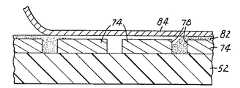
노출된 구리는 종래 기술, 예를 들면 5% 묽은 황산 용액을 사용하여 세척하거나 에칭하여 제15 단계에서 추가로 전기 도금하기 위한 표면을 제조한 뒤, 제17 단계에서 추가로 전기 도금 과정에 적용시켜 노출 영역에서 추가량의 구리를 증착시킴으로써 제4도의 물품(68)에 도시된 바와 같이 일체형 마스크(70)를 형성한다. 구리 마스크(70)는 이후에 도포될 패턴 물질의 예상 높이와 동일하거나 또는 이를 초과하는 높이로 보강된다. 그 높이는, 마스크(70)가 이후에 도포되는 패턴 물질(74)의 경계가 되기에 충분해야 하며, 제5도와 관련하여 설명되는 바와 같이 구리 마스크가 후속 단계의 에칭 처리를 받기에 충분해야 한다. 통상적으로 얇은 필름 물질을 마스킹하기에는 2밀 이하의 높이가 충분하다. 그러나, 상한치는 증착되는 마스크 물질(70)의 일체성, 증착되는 패턴 물질의 특성, 후속적으로 패턴 물질(74)이 증착됨에 따른 마스크(70)의 방해도와 같은 실질적인 사항을 근거로 한다.The exposed copper may be washed or etched using prior art, e.g., 5% dilute sulfuric acid solution to produce a surface for further electroplating in
패턴 물질의 두께는 일반적으로 0.1㎛ 이상이다. 일부 용도의 경우에는, 0.5㎛이상의 비교적 두꺼운 필름이 유용하며 1 또는 2㎛ 또는 그 이상의 두께를 지닐 수 있다. 상술한 바와 같이, 2밀(50㎛) 이상의 두께를 지닐 수 있는 보다 얇은 필름을 필요에 따라 제조할 수 있는데, 이는 마스크의 높이에 의해서만 제한된다.The thickness of the pattern material is generally at least 0.1 μm. For some applications, relatively thick films of 0.5 μm or more are useful and may have a thickness of 1 or 2 μm or more. As mentioned above, thinner films which can have a thickness of at least 2 mils (50 μm) can be produced as required, which is limited only by the height of the mask.
상기 방법은, 마스크 물질(70)로서 구리를 사용하는 것과 관련하여 본문에 기술된 반면, 패턴 물질(74)에 나쁜 영향을 주지 않고 선택적으로 제거될 수 있는 유기 물질과 같이 다른 흔히 사용되는 에칭 가능한 금속을 사용할 수 있다. 따라서, 여러가지 용해성 또는 박리성 중합체는, 유용한 마스크를 형성하기에 충분한 일체성 및 안정성을 지니고, 증착 방법 또는 패턴 물질(74)에 의해서 나쁜 영향을 받지 않으며, 선택적으로 제거될 수 있는 한, 마스크 물질(70)로서 사용될 수 있다. 잠재적인 마스크 물질의 예는 패턴 물질에 나쁜 영향을 끼칠 정도로 용융, 분해 또는 탈기되지 않는 증착 방법의 온도를 지탱할 수 있는 유기 포토레지스트 등이다.The method is described herein in connection with the use of copper as the
일체 마스크(70)의 증착이 완료되면, 제19 단계에서 종래 기술을 통해 나머지 가교 결합된 포토레지스트(58')를 제거하고, 포토레지스트(58')에 의해 미리 보호된 구리 하부층(56)을 위치(21)에서 플래쉬 에칭 방식으로 제거한다. 마스크 물질(70)의 일부 소부분은 제거할 수도 있으나, 그 양은 실질적으로 마스크에 영향을 미치기에는 충분하지 않다. 어떤 경우에 있어서, 증착된 마스크(70)의 높이는, 플래시 에칭 방법을 사용할 경우, 플래시 에칭 단계에서 선택함으로써, 플래쉬 에칭후에 남아 있는 양이 적당한 마스크를 제공하도록 해야 한다.After the deposition of the
본 발명의 또 다른 실시 양태에서는 부가 방법보다는 삭감 방법으로 마스크를 제조한다. 즉, 제1도 내지 제4도와 관련하여 기술된 바와 같은 구리 스크린의 보강 보다는, 두꺼운 호일을 폴리이미드 시이트와 같은 기판에 적층하고 상술한 바와 같이 포토레지스트 기술을 사용하여, 구리의 원치 않는 부분을 에칭 제거하여 제4도에 도시된 바와 같이 구리 스크린 또는 마스크만 남도록 한다.In another embodiment of the present invention, the mask is manufactured by a reduction method rather than an addition method. That is, rather than the reinforcement of copper screens as described in connection with FIGS. 1 through 4, thick foils are laminated to a substrate such as a polyimide sheet and photoresist techniques as described above to remove unwanted portions of copper. The etching is removed to leave only the copper screen or mask as shown in FIG.
이 방법의 실행시에는, 시판되는 폴리이미드/구리 적층 복합체를 출발 물질로 사용하고, 추가량의 구리 전기 도금을 제거하여 제15 단계 및 제17 단계에서 일체 마스크를 형성하는 것이 바람직하다. 또한, 제9 단계 내지 제13 단계와 관련하여, 포토레지스트를 구리 호일에 적층시키고, 스텐실을 통해 광선에 노출시킨다. 삭감 기술의 경우에는 패턴 물질을 증착시키고자 할 때 포토레지스트를 제거/현상시키고, 제4도에 도시한 바와 같이 상기 영역에서 구리를 에칭 제거함으로서 기판(52)(하부층(56) 이하)상에 일체 마스크(70)를 제공한다. 나머지 포토레지스트를 제거한 후, 마스크 형상을 위해 부가 기술을 사용하는 경우와 동일한 방식으로 상기 물질을 처리한다.In the practice of this method, it is preferable to use commercially available polyimide / copper laminate composites as starting materials and to remove additional amounts of copper electroplating to form integral masks in
정밀하게 배치된 일체 마스크(70)는 이제 제4도에 도시된 바와 같이 가요성기판(52)상에 형성되어 있으며, 이때 패턴 물질(74)은 일체 마스크(70)를 지닌 기판상에 증착될 수 있다. 패턴 물질은 원하는 장식 또는 실용 기능을 제공하는 에칭하기 어려운 많은 물질, 예를 들어 금속, 합금, 세라믹, 및 유기 중합체 물질 중 임의의 것일 수 있다.A precisely disposed
은, 텅스텐 또는 탄소와 같은 전도성 금속이 유용할 수 있다. 특정 세라믹, 자기, 절연 및 특정의 순수 장식 재료도, 많은 용도에 유리하게 사용될 수 있다.Conductive metals such as silver, tungsten or carbon may be useful. Certain ceramics, porcelains, insulations and certain purely decorative materials can also be advantageously used in many applications.
종래의 많은 증착 기술은 위치(23)에서 일어나는 단계에 사용할 수 있다. 그러나, 제한된 사출력을 가진 기술을 사용하여 일부 마스크(70)의 수직 표면중 일부가 개방되거나 밀봉하지 않음에 따라 패턴 물질에 역효과를 주지 않는 구리 에칭제와 같은 마스크-특이 제거제에 마스크(70)를 접근시켜 마스크(70)를 연속 제거하는 것이 바람직하다. 또한, 증착 방법은 마스크 물질에 역효과를 주지 않는 온도에서 진행되어야 한다.Many conventional deposition techniques can be used for the steps that occur at location 23. However,
실제로, 각종 증기 증착 방법을 사용하여 패턴 물질을 증착시키는 것이 유용한 것으로 밝혀졌다. 실례로는, 금속 합금 증착에 전자 광선 증발법을 사용할 수 있고,비전도성 물질에는 유도 증발법을 사용할 수 있다. 이들 방법들은 불량한 사출력을 보인다. 즉, 이들은 증착 물질의 스트림이 거의 방해없이 직선 및 평행선상에 있기 때문에, 기판면에 수직인 표면상에 매우 적은 물질을 증착시키는 경향이 있다. 바꿔 말하면, 불량한 사출력은 물질의 방출류에 평행한 면이 거의 코팅 또는 밀봉되지 않는다는 것을 의미한다. 그러므로, 마스크 수직면은 패턴 물질에 의해 덮히거나 또는 밀봉되지 않을 것이다.Indeed, it has been found useful to deposit pattern materials using various vapor deposition methods. For example, electron beam evaporation can be used for metal alloy deposition, and inductive evaporation can be used for non-conductive materials. These methods show poor dead power. That is, they tend to deposit very little material on a surface perpendicular to the substrate plane because the stream of deposition material is straight and parallel with almost no obstruction. In other words, poor dead power means that the plane parallel to the discharge flow of material is hardly coated or sealed. Therefore, the mask vertical plane will not be covered or sealed by the pattern material.
패턴 물질(74)은 마스크(70)의 높이가 과도하게 높지 않는 한, 바람직한 두께로 증착될 수 있다. 마스크(70)가 완전히 덮힌 경우에는 에칭에 의한 때와 같이 연속적인 제거를 위한 접근점이 없다. 패턴 물질(70)의 단일층 또는 다중층은 증착될 수 있다. 패턴 물질(74)의 층은 소정 목적을 수행하는데 충분히 상용성이 있는 한, 예를 들면 서로 접착하여 바람직하지 않게 화학적으로 반응하지 않는 한 동일하거나 다를 수 있다.The
제9도는 패턴 물질을 연속적으로 증착하기 위한 패턴 장치(32)의 개략도를 나타낸다. 장치(32)는 마스크가 덮힌 기판(68)이 감긴 가역적 감김 및 공급 리일(33,34)로 구성되어 있다. 기판(68)은, 인장 롤러(35,36), 및 필요에 따라서 가열 또는 냉각될 수 있는 가역 코팅 로울(37)위를 통과한다. 두개의 별도의 증착지점(39,43)이 나타나 있다. 이들은 동일하거나 다를 수 있다. 두개가 제시되어 있으나, 이들 방법에서는 한 지점만을 사용할 수도 있고, 일부 용도에서는 두개 이상의 지점이 유용할 수도 있다.9 shows a schematic diagram of a
작동시, 기판(68)을 먼저 한개 또는 양 지점(39,43)에서 코팅한후, 로올(37) 주위에 공급 리일(33)로부터 공급하여 로올(34)위에 감는다. 기판(68)의 속도는, 소정량의 패턴 물질이 기판(68)위에 증착되도록 선택된다. 한 방향으로 코팅하는 위치(39)와 다른 방향으로 코팅하는 위치(43)를 사용하여 로올(33,34)의 방향을 바꿈으로써 다른 물질로 이루어진 이루어진 교번층을 증착할 수 있다. 대안적으로 어느 방향으로든 작동시켜 다양한 층 효과를 제공할 때에는 두 코팅 위치를 동시에 작동시킬 수 있다.In operation, the
39,43으로 표시된 증착 지점은, 증착될 패턴 물질에 대해 제한된 사출력을 지닌 각종 공지된 증착 시스템일 수 있다. 고체 금속은 전자 광선 증발법과 같은 증발 기술에 의해 증착될 수 있다. 비금속 고체 물질도 유도 또는 저항 증발법 등과 같은 종래 기술로 증착시킬 수 있다.The deposition points, denoted 39,43, may be various known deposition systems with limited dead power for the pattern material to be deposited. Solid metals may be deposited by evaporation techniques such as electron beam evaporation. Nonmetallic solid materials may also be deposited by conventional techniques such as inductive or resistive evaporation.
패턴 물질 증착이 완결되면, 제품(72)은 제5도에 나타난 것과 유사한 단면을 지니게 되며, 이때 패턴 물질(74)은 증착 스트림에 수직인 구리 마스크(70)의 표면상에 증착된다. 마스크(70)의 수직 벽중 상당 부분이 패턴 물질(74)의 보강부에 의해 차단될 지라도, 마스크의 상부 근처에 있는 일부 구리 마스크(70)는 차단되지 않고 노출된 상태로 남아 있어 마스크-특이 제거제에 의해 후속적 공격을 받을 수 있다.Once the pattern material deposition is complete, the
패턴 증착후, 마스크 물질(70,56)은 제25 단계에 제시된 바와 같이 제거될 수 있다. 통상적으로, 마스크 물질(70,56)은 에칭성 금속이므로 마스크 물질(70)에 특이성인 화학적 에칭제, 예를 들어 구리의 경우 황산에 의해 제거됨에 따라 패턴 물질(74)을 제자리에 남길 수 있다.After pattern deposition, the
기판 프라이머(54)를 사용했다면(제2도 참조) 제27 단계에서 제거한다. 프라이머층을 제거하는데 사용된 화학 물질을 공격하지 않아야 한다. 패턴화된 제품(76)의 단면은 제6도에 나타나 있으며, 여기에서 패턴 물질(74)의 수직 테두리(78)는 마스크 물질(70)의 제거에 의해 남겨진 공극으로 분리된다.If the
패턴화된 제품(80)의 상면도는 제8도에 나타나 있으며, 여기에서 패턴 물질(74)은 그것의 테두리(78)에 의해 형성된 정확하게 조절된 공간으로 분리된 각종 패턴으로 제시되어 있다. 이들 공간의 폭 및 정확성을 스텐실(60)을 제조하는데 유용한 기술, 과도한 마스크 높이에 의해 야기되는 음영 효과의 제어, 에칭 물질의 적당한 선택, 에칭 조건 등에 의해 좌우된다.A top view of the patterned article 80 is shown in FIG. 8, where the
제1도에 도시된 공정의 위치(29)에서, 패턴화된 제품상에 대해 많은 전환 조작을 수행할 수 있다. 예를 들어, 물품은 각종 모양으로 절단, 슬릿화 또는 펀치 처리될 수 있다. 보호성 또는 접착성 물질층(82)을 부가하여 오염을 방지하거나, 여기에 부가적인 물질을 결합시킬 수 있다. 패턴화된 가요성 제품은 의도된 궁극적인 목적에 따라 로울화, 적재 또는 적층화될 수 있다. 접착층은 제7도에 도시된 바와 같이 릴리이스 라이너(84)를 가질 수 있다.At position 29 of the process shown in FIG. 1, many switching operations can be performed on the patterned product phase. For example, the article can be cut, slitted or punched into various shapes. A protective or
본 발명의 패턴화된 제품은 인쇄 회로 기판 등과 같은 각종 장식 또는 전기 용도에 유용성이 있는데, 이때 패턴은 탄소의 전도성 패턴, 에칭이 곤란한 초전도성 물질 등으로 구성된다.The patterned article of the present invention is useful for a variety of decorative or electrical applications such as printed circuit boards, wherein the pattern consists of a conductive pattern of carbon, a superconducting material that is difficult to etch, and the like.
본 발명의 또 다른 실시 태양에서는 제1도에 도시된 방법을 조절하여 패턴 물질 입자의 정확한 성형편을 제공할 수 있다. 보다 구체적으로, 패턴화 공정은 제1도에 도시된 바와 같이 실행하되, 돌출된 마스크 바로 밑이 아닌 일부 마스크 물질(56)(제2도-제5도 참조)을 제거하기 위하여 대개 제21 단계에서 수행된 플래쉬 에칭 단계를 생략한다.In another embodiment of the present invention, the method shown in FIG. 1 can be adjusted to provide accurate shaped pieces of patterned material particles. More specifically, the patterning process is carried out as shown in FIG. 1, but usually takes place in
이러한 단계를 생략함에 따라, 패턴 물질(74)은 마스크 하부층(56)의 상부에 증착된다. 따라서, 마스크 물질(70)의 후속적 에칭이 이루어지면, 제1도의 위치(25)에 지시된 바와 같이 패턴 물질(74)하의 구리 하부층(56)이 또한 부착되고 패턴 물질(74)은 하부층(52)으로부터 분리된다. 패턴 물질(74)이 별도의 섬모양인 경우, 패턴 물질의 소편 또는 입자가 얻어진다. 이들은 장사(長絲)형, 사각형, 원형 또는 다른 바람직한 기하학적 형태일 수 있으며, 상기 공정에서와 같이 하나 이상의 물질 층으로 구성될 수 있다. 입자의 크기 분포는 사용된 패턴에 의해 조절될 수 있다. 입자의 혼합물은, 좁고 거의 균일한 크기 분포로부터 매우 넓은 크기 분포를 가진 입자 크기 분포를 가질 수 있다. 사용되는 입자내의 다중층의 두께도 조절될 수 있다.By omitting this step, the
이렇게 수득된 조각 또는 입자는 단독으로 또는 다른 물질과의 혼합물로 유용할 수 있다. 예를 들어, 이들은 각종 부형제 또는 매트릭스에 배합되어 보강된 플라스틱 조성물, 코팅, 페이트 등을 제공할 수 있다. 대안적으로, 이들은 그 조성에 따라서 연마 또는 광학적 작용 물질로서 유용할 수 있다.The pieces or particles thus obtained may be useful alone or in admixture with other materials. For example, they can be formulated into various excipients or matrices to provide reinforced plastic compositions, coatings, pates, and the like. Alternatively, they may be useful as abrasive or optically acting materials, depending on their composition.
상기 방법은 보다 특이성의 물질에 관하여 기술하였다. 그러나, 본 발명은 당업자에 의해 쉽게 이용될 수 있다는 것이 명백하다.The method has been described with regard to more specific substances. However, it is apparent that the present invention can be easily used by those skilled in the art.
[실시예]EXAMPLE
본 발명의 실행을 검증하기 위하여, 인쇄 회로 장치를 제조한다. 이러한 장치를 제조하기 위하여, 가요성 폴리이미드 필름(캡톤, 듀퐁사)의 한 표면을 스퍼터증착 방식에 의해 구리로 코팅하였다. 0.5밀(13μm) 두께의 양성 작용 포토레지스트 층을 구리 코팅에 적층하고, 포토레지스트층을 노출시킨 다음, 스텐실로서 음각 인쇄 회로를 사용하여 현상하였다.In order to verify the implementation of the present invention, a printed circuit device is manufactured. In order to make such a device, one surface of a flexible polyimide film (Kapton, DuPont) was coated with copper by sputter deposition. A 0.5 mil (13 μm) thick positive acting photoresist layer was laminated to the copper coating, the photoresist layer was exposed and developed using a negative printed circuit as a stencil.
포토레지스트 물질이 현상에 의해 제거되는 영역에서, 구리를 전기 도금하여 높이가 약 0.5밀(13μm) 미만인 마스크를 제공하였다. 이어서, 나머지 포토레지스트를 제거하고, 산/아크롬산 칼륨 에칭제를 사용하여 샘플을 플래쉬 에칭함으로써 비-마스크 영역의 필름을 제거하였다.In areas where the photoresist material is removed by development, copper was electroplated to provide a mask less than about 0.5 mil (13 μm) in height. The remaining photoresist was then removed and the film in the non-mask area was removed by flash etching the sample using an acid / potassium chromite etchant.
이어서 마스크 시이트를 진공실에 넣고, 수백 옹스트롬(Å)의 탄소로 코팅하였다. 이어서, 황산/이크롬산 칼륨 에칭제를 사용하여 구리 마스크 물질을 에칭하여 폴리이미드 기판상에 탄소의 인쇄 회로 패턴을 남겼다.The mask sheet was then placed in a vacuum chamber and coated with several hundred angstroms of carbon. The copper mask material was then etched using a sulfuric acid / potassium dichromate etchant to leave a printed circuit pattern of carbon on the polyimide substrate.
Claims (1)
Translated fromKoreanApplications Claiming Priority (2)
| Application Number | Priority Date | Filing Date | Title |
|---|---|---|---|
| US07/281,655US4964945A (en) | 1988-12-09 | 1988-12-09 | Lift off patterning process on a flexible substrate |
| US281,655 | 1988-12-09 |
Publications (2)
| Publication Number | Publication Date |
|---|---|
| KR900010472A KR900010472A (en) | 1990-07-07 |
| KR0169959B1true KR0169959B1 (en) | 1999-05-01 |
Family
ID=23078237
Family Applications (1)
| Application Number | Title | Priority Date | Filing Date |
|---|---|---|---|
| KR1019890018260AExpired - Fee RelatedKR0169959B1 (en) | 1988-12-09 | 1989-12-08 | Patterning process and microparticles of substantially the same geometry and shape |
Country Status (7)
| Country | Link |
|---|---|
| US (2) | US4964945A (en) |
| JP (1) | JP2744826B2 (en) |
| KR (1) | KR0169959B1 (en) |
| CA (1) | CA2002736A1 (en) |
| DE (1) | DE3940087A1 (en) |
| GB (1) | GB2228372B (en) |
| MY (1) | MY104668A (en) |
Families Citing this family (81)
| Publication number | Priority date | Publication date | Assignee | Title |
|---|---|---|---|---|
| DE69026339T2 (en)* | 1989-11-13 | 1996-08-14 | Fujitsu Ltd | Josephson Transition Apparatus |
| US5196395A (en)* | 1991-03-04 | 1993-03-23 | Superconductor Technologies, Inc. | Method for producing crystallographic boundary junctions in oxide superconducting thin films |
| US5246538A (en)* | 1991-09-16 | 1993-09-21 | Phillips Petroleum Company | Adhesive bonding of poly(arylene sulfide) surfaces |
| JPH05129760A (en)* | 1991-11-06 | 1993-05-25 | Fujitsu Ltd | Method of forming conductor pattern |
| US5362534A (en)* | 1993-08-23 | 1994-11-08 | Parlex Corporation | Multiple layer printed circuit boards and method of manufacture |
| US5376232A (en)* | 1993-08-23 | 1994-12-27 | Parlex Corporation | Method of manufacturing a printed circuit board |
| US5522963A (en)* | 1994-05-31 | 1996-06-04 | International Business Machines Corporation | Method for machining and depositing metallurgy on ceramic layers |
| KR100427708B1 (en)* | 1994-11-18 | 2004-07-16 | 가부시키가이샤 한도오따이 에네루기 켄큐쇼 | Display device board member manufacturing method and manufacturing device |
| US5814567A (en)* | 1996-06-14 | 1998-09-29 | Kimberly-Clark Worldwide, Inc. | Durable hydrophilic coating for a porous hydrophobic substrate |
| JP3217999B2 (en) | 1997-12-03 | 2001-10-15 | セイコーインスツルメンツ株式会社 | Component manufacturing method and component manufacturing device |
| US6873087B1 (en)* | 1999-10-29 | 2005-03-29 | Board Of Regents, The University Of Texas System | High precision orientation alignment and gap control stages for imprint lithography processes |
| AU2001273491A1 (en) | 2000-07-16 | 2002-02-05 | Board Of Regents, The University Of Texas System | High-resolution overlay alignment methods and systems for imprint lithography |
| CN1262883C (en) | 2000-07-17 | 2006-07-05 | 得克萨斯州大学系统董事会 | Method and system of automatic fluid dispensing for imprint lithography processes |
| JP2004505273A (en) | 2000-08-01 | 2004-02-19 | ボード・オブ・リージエンツ,ザ・ユニバーシテイ・オブ・テキサス・システム | Method for highly accurate sensing of gap and orientation between transparent template and substrate for transfer lithography |
| AU2001286573A1 (en) | 2000-08-21 | 2002-03-04 | Board Of Regents, The University Of Texas System | Flexure based macro motion translation stage |
| EP1352295B1 (en)* | 2000-10-12 | 2015-12-23 | Board of Regents, The University of Texas System | Template for room temperature, low pressure micro- and nano-imprint lithography |
| US6964793B2 (en) | 2002-05-16 | 2005-11-15 | Board Of Regents, The University Of Texas System | Method for fabricating nanoscale patterns in light curable compositions using an electric field |
| WO2003048726A2 (en)* | 2001-11-30 | 2003-06-12 | Tracking Technology Inc. | Taggants for products and method of taggant identification |
| DE50310646D1 (en)* | 2002-04-15 | 2008-11-27 | Schott Ag | METHOD OF COATING METAL SURFACES |
| US7037639B2 (en) | 2002-05-01 | 2006-05-02 | Molecular Imprints, Inc. | Methods of manufacturing a lithography template |
| US6926929B2 (en) | 2002-07-09 | 2005-08-09 | Molecular Imprints, Inc. | System and method for dispensing liquids |
| US6932934B2 (en) | 2002-07-11 | 2005-08-23 | Molecular Imprints, Inc. | Formation of discontinuous films during an imprint lithography process |
| US6900881B2 (en) | 2002-07-11 | 2005-05-31 | Molecular Imprints, Inc. | Step and repeat imprint lithography systems |
| US7077992B2 (en) | 2002-07-11 | 2006-07-18 | Molecular Imprints, Inc. | Step and repeat imprint lithography processes |
| US7019819B2 (en) | 2002-11-13 | 2006-03-28 | Molecular Imprints, Inc. | Chucking system for modulating shapes of substrates |
| US6908861B2 (en)* | 2002-07-11 | 2005-06-21 | Molecular Imprints, Inc. | Method for imprint lithography using an electric field |
| US6916584B2 (en) | 2002-08-01 | 2005-07-12 | Molecular Imprints, Inc. | Alignment methods for imprint lithography |
| US7027156B2 (en) | 2002-08-01 | 2006-04-11 | Molecular Imprints, Inc. | Scatterometry alignment for imprint lithography |
| US7070405B2 (en) | 2002-08-01 | 2006-07-04 | Molecular Imprints, Inc. | Alignment systems for imprint lithography |
| US7071088B2 (en) | 2002-08-23 | 2006-07-04 | Molecular Imprints, Inc. | Method for fabricating bulbous-shaped vias |
| US8349241B2 (en) | 2002-10-04 | 2013-01-08 | Molecular Imprints, Inc. | Method to arrange features on a substrate to replicate features having minimal dimensional variability |
| US6980282B2 (en) | 2002-12-11 | 2005-12-27 | Molecular Imprints, Inc. | Method for modulating shapes of substrates |
| US6929762B2 (en) | 2002-11-13 | 2005-08-16 | Molecular Imprints, Inc. | Method of reducing pattern distortions during imprint lithography processes |
| US6871558B2 (en)* | 2002-12-12 | 2005-03-29 | Molecular Imprints, Inc. | Method for determining characteristics of substrate employing fluid geometries |
| US7452574B2 (en) | 2003-02-27 | 2008-11-18 | Molecular Imprints, Inc. | Method to reduce adhesion between a polymerizable layer and a substrate employing a fluorine-containing layer |
| US20040175843A1 (en)* | 2003-03-04 | 2004-09-09 | Roitman Daniel B. | Near-field and far-field encoding and shaping of microbeads for bioassays |
| US20040175842A1 (en)* | 2003-03-04 | 2004-09-09 | Roitman Daniel B. | Near-field and far-field encoding of microbeads for bioassays |
| US7179396B2 (en) | 2003-03-25 | 2007-02-20 | Molecular Imprints, Inc. | Positive tone bi-layer imprint lithography method |
| US7122079B2 (en) | 2004-02-27 | 2006-10-17 | Molecular Imprints, Inc. | Composition for an etching mask comprising a silicon-containing material |
| US7396475B2 (en) | 2003-04-25 | 2008-07-08 | Molecular Imprints, Inc. | Method of forming stepped structures employing imprint lithography |
| US7157036B2 (en) | 2003-06-17 | 2007-01-02 | Molecular Imprints, Inc | Method to reduce adhesion between a conformable region and a pattern of a mold |
| US7136150B2 (en) | 2003-09-25 | 2006-11-14 | Molecular Imprints, Inc. | Imprint lithography template having opaque alignment marks |
| US7090716B2 (en) | 2003-10-02 | 2006-08-15 | Molecular Imprints, Inc. | Single phase fluid imprint lithography method |
| US8211214B2 (en) | 2003-10-02 | 2012-07-03 | Molecular Imprints, Inc. | Single phase fluid imprint lithography method |
| EP3242318A1 (en) | 2003-12-19 | 2017-11-08 | The University of North Carolina at Chapel Hill | Monodisperse micro-structure or nano-structure product |
| US9040090B2 (en) | 2003-12-19 | 2015-05-26 | The University Of North Carolina At Chapel Hill | Isolated and fixed micro and nano structures and methods thereof |
| US8076386B2 (en) | 2004-02-23 | 2011-12-13 | Molecular Imprints, Inc. | Materials for imprint lithography |
| US7906180B2 (en) | 2004-02-27 | 2011-03-15 | Molecular Imprints, Inc. | Composition for an etching mask comprising a silicon-containing material |
| CA2618148A1 (en) | 2005-08-12 | 2007-02-22 | Dunwilco (1198) Limited | Process for producing metal flakes |
| US8178278B2 (en)* | 2005-09-13 | 2012-05-15 | Affymetrix, Inc. | Miniaturized microparticles |
| EP2485052B1 (en)* | 2005-09-13 | 2015-05-06 | Affymetrix, Inc. | Encoded microparticles |
| KR20070047114A (en)* | 2005-11-01 | 2007-05-04 | 주식회사 엘지화학 | Manufacturing method of device with flexible substrate and device with flexible substrate manufactured by the same |
| US7906058B2 (en) | 2005-12-01 | 2011-03-15 | Molecular Imprints, Inc. | Bifurcated contact printing technique |
| US7803308B2 (en) | 2005-12-01 | 2010-09-28 | Molecular Imprints, Inc. | Technique for separating a mold from solidified imprinting material |
| MY144847A (en) | 2005-12-08 | 2011-11-30 | Molecular Imprints Inc | Method and system for double-sided patterning of substrates |
| US7670530B2 (en) | 2006-01-20 | 2010-03-02 | Molecular Imprints, Inc. | Patterning substrates employing multiple chucks |
| KR100650869B1 (en)* | 2005-12-30 | 2006-11-28 | 동부일렉트로닉스 주식회사 | STI Formation Method of Semiconductor Device |
| EP1999873A2 (en)* | 2006-03-13 | 2008-12-10 | SMI Holding, Inc. | Automatic microparticle mark reader |
| US7749396B2 (en)* | 2006-03-24 | 2010-07-06 | Palo Alto Research Center Incorporated | Method of manufacturing fine features for thin film transistors |
| US7524768B2 (en)* | 2006-03-24 | 2009-04-28 | Palo Alto Research Center Incorporated | Method using monolayer etch masks in combination with printed masks |
| US8142850B2 (en) | 2006-04-03 | 2012-03-27 | Molecular Imprints, Inc. | Patterning a plurality of fields on a substrate to compensate for differing evaporation times |
| US7802978B2 (en) | 2006-04-03 | 2010-09-28 | Molecular Imprints, Inc. | Imprinting of partial fields at the edge of the wafer |
| US8850980B2 (en) | 2006-04-03 | 2014-10-07 | Canon Nanotechnologies, Inc. | Tessellated patterns in imprint lithography |
| TW200801794A (en) | 2006-04-03 | 2008-01-01 | Molecular Imprints Inc | Method of concurrently patterning a substrate having a plurality of fields and a plurality of alignment marks |
| US8012395B2 (en) | 2006-04-18 | 2011-09-06 | Molecular Imprints, Inc. | Template having alignment marks formed of contrast material |
| US7547398B2 (en) | 2006-04-18 | 2009-06-16 | Molecular Imprints, Inc. | Self-aligned process for fabricating imprint templates containing variously etched features |
| GB2440140A (en)* | 2006-07-17 | 2008-01-23 | Dunwilco | Method of making flakes |
| WO2008011051A1 (en)* | 2006-07-17 | 2008-01-24 | Liquidia Technologies, Inc. | Nanoparticle fabrication methods, systems, and materials |
| CA2669540A1 (en)* | 2006-11-14 | 2008-07-17 | Contra Vision Ltd. | Improvements to printing superimposed layers |
| US20100151031A1 (en)* | 2007-03-23 | 2010-06-17 | Desimone Joseph M | Discrete size and shape specific organic nanoparticles designed to elicit an immune response |
| US20120281980A1 (en)* | 2010-01-29 | 2012-11-08 | Cho Hans S | Optical sensor networks and methods for fabricating the same |
| US10158061B2 (en)* | 2013-11-12 | 2018-12-18 | Varian Semiconductor Equipment Associates, Inc | Integrated superconductor device and method of fabrication |
| US9947441B2 (en) | 2013-11-12 | 2018-04-17 | Varian Semiconductor Equipment Associates, Inc. | Integrated superconductor device and method of fabrication |
| US10615949B2 (en) | 2014-02-14 | 2020-04-07 | University Of Southern California | Hybrid-based cancellation in presence of antenna mismatch |
| US10581650B2 (en) | 2015-09-08 | 2020-03-03 | Qorvo Us, Inc. | Enhancing isolation in radio frequency multiplexers |
| US9912326B2 (en) | 2015-09-08 | 2018-03-06 | Abtum Inc. | Method for tuning feed-forward canceller |
| US9866201B2 (en) | 2015-09-08 | 2018-01-09 | Abtum Inc. | All-acoustic duplexers using directional couplers |
| US10038458B2 (en) | 2015-10-06 | 2018-07-31 | Abtum Inc. | Reflection-based radio-frequency multiplexers |
| CN108352915B (en) | 2015-10-12 | 2020-06-30 | Qorvo美国公司 | Radio frequency multiplexer based on hybrid coupler |
| WO2018057725A1 (en) | 2016-09-21 | 2018-03-29 | Abtum Inc. | Enhancing isolation in hybrid-based radio frequency duplexers and multiplexers |
| US11124659B2 (en)* | 2018-01-30 | 2021-09-21 | Lam Research Corporation | Method to selectively pattern a surface for plasma resistant coat applications |
Family Cites Families (33)
| Publication number | Priority date | Publication date | Assignee | Title |
|---|---|---|---|---|
| US3192136A (en)* | 1962-09-14 | 1965-06-29 | Sperry Rand Corp | Method of preparing precision screens |
| US3499956A (en)* | 1965-03-22 | 1970-03-10 | Johns Manville | Process for making thermoplastic decorative covering material |
| US3540047A (en)* | 1968-07-15 | 1970-11-10 | Conductron Corp | Thin film magnetodielectric materials |
| FR2029413A1 (en)* | 1969-01-29 | 1970-10-23 | Comp Generale Electricite | Making integrated silicon semiconductors |
| US3526573A (en)* | 1969-06-11 | 1970-09-01 | Westinghouse Electric Corp | Flexible flame retardant foil-clad laminates |
| US3728177A (en)* | 1970-07-30 | 1973-04-17 | Olin Corp | Method of producing a flexible laminate copper circuit |
| US3846118A (en)* | 1971-03-24 | 1974-11-05 | Graham Magnetics Inc | Process for making small particles |
| US3988494A (en)* | 1972-04-10 | 1976-10-26 | Mobil Oil Corporation | Metallizing coating compositions |
| US3799777A (en)* | 1972-06-20 | 1974-03-26 | Westinghouse Electric Corp | Micro-miniature electronic components by double rejection |
| US4053433A (en)* | 1975-02-19 | 1977-10-11 | Minnesota Mining And Manufacturing Company | Method of tagging with color-coded microparticles |
| CA1056653A (en)* | 1975-11-10 | 1979-06-19 | Edward J. Stevens | Color-coded identifier microparticles |
| JPS5358224A (en)* | 1976-11-05 | 1978-05-26 | Matsushita Electric Ind Co Ltd | Composite diaphragm for speakers |
| JPS5496775A (en)* | 1978-01-17 | 1979-07-31 | Hitachi Ltd | Method of forming circuit |
| JPS6019608B2 (en)* | 1978-10-03 | 1985-05-17 | シャープ株式会社 | Electrode pattern formation method |
| US4390452A (en)* | 1979-08-20 | 1983-06-28 | Minnesota Mining & Manufacturing Company | Microparticles with visual identifying means |
| JPS5669835A (en)* | 1979-11-09 | 1981-06-11 | Japan Electronic Ind Dev Assoc<Jeida> | Method for forming thin film pattern |
| DE3204425A1 (en)* | 1982-02-09 | 1983-08-25 | Siemens AG, 1000 Berlin und 8000 München | METHOD FOR PRODUCING SUPPORTING METAL GRID STRUCTURES |
| US4621030A (en)* | 1982-07-19 | 1986-11-04 | Hitachi, Ltd. | Perpendicular magnetic recording medium and manufacturing method thereof |
| US4474845A (en)* | 1982-08-26 | 1984-10-02 | General Motors Corporation | Compacted sheet molding compound |
| JPS59215790A (en)* | 1983-05-23 | 1984-12-05 | マルイ工業株式会社 | Method of producing printed circuit board |
| JPS59229727A (en)* | 1983-06-09 | 1984-12-24 | Matsushita Electric Ind Co Ltd | Fine processing method of thin film |
| US4606788A (en)* | 1984-04-12 | 1986-08-19 | Moran Peter L | Methods of and apparatus for forming conductive patterns on a substrate |
| US4568529A (en)* | 1984-09-21 | 1986-02-04 | Thermo-Formage Mediterraneen | Thermoplastic composite material for the preparation of moulded objects, particularly by injection, and a process for making same |
| US4698021A (en)* | 1985-01-11 | 1987-10-06 | Itzhak Shoher | Metal foil for forming a dental coping and crown |
| JPS61242044A (en)* | 1985-04-19 | 1986-10-28 | Matsushita Electronics Corp | Manufacture of semiconductor device |
| JPS6260662A (en)* | 1985-09-11 | 1987-03-17 | Alps Electric Co Ltd | Manufacture of thermal heads |
| GB8610024D0 (en)* | 1986-04-24 | 1986-05-29 | Unilever Plc | Porous structures |
| US4711814A (en)* | 1986-06-19 | 1987-12-08 | Teichmann Robert J | Nickel particle plating system |
| WO1988005990A1 (en)* | 1987-02-05 | 1988-08-11 | Hughes Aircraft Company | Cladding of substrates with thick metal circuit patterns |
| US4849284A (en)* | 1987-02-17 | 1989-07-18 | Rogers Corporation | Electrical substrate material |
| US4816347A (en)* | 1987-05-29 | 1989-03-28 | Avco Lycoming/Subsidiary Of Textron, Inc. | Hybrid titanium alloy matrix composites |
| ES2040343T3 (en)* | 1987-06-08 | 1993-10-16 | Esselte Meto International Gmbh | MAGNETIC DEVICES. |
| US4877689A (en)* | 1988-09-30 | 1989-10-31 | United States Of America As Represented By The Administrator, National Aeronautics And Space Administration | High temperature insulation barrier composite |
- 1988
- 1988-12-09USUS07/281,655patent/US4964945A/ennot_activeExpired - Fee Related
- 1989
- 1989-11-10CACA002002736Apatent/CA2002736A1/ennot_activeAbandoned
- 1989-11-13MYMYPI89001582Apatent/MY104668A/enunknown
- 1989-11-24GBGB8926659Apatent/GB2228372B/ennot_activeExpired - Fee Related
- 1989-12-04DEDE3940087Apatent/DE3940087A1/ennot_activeWithdrawn
- 1989-12-08JPJP1320408Apatent/JP2744826B2/ennot_activeExpired - Lifetime
- 1989-12-08KRKR1019890018260Apatent/KR0169959B1/ennot_activeExpired - Fee Related
- 1992
- 1992-09-14USUS07/944,716patent/US5294476A/ennot_activeExpired - Fee Related
Also Published As
| Publication number | Publication date |
|---|---|
| DE3940087A1 (en) | 1990-06-13 |
| CA2002736A1 (en) | 1990-06-09 |
| JPH02260492A (en) | 1990-10-23 |
| KR900010472A (en) | 1990-07-07 |
| JP2744826B2 (en) | 1998-04-28 |
| US5294476A (en) | 1994-03-15 |
| US4964945A (en) | 1990-10-23 |
| GB2228372A (en) | 1990-08-22 |
| MY104668A (en) | 1994-05-31 |
| GB2228372B (en) | 1993-06-23 |
| GB8926659D0 (en) | 1990-01-17 |
Similar Documents
| Publication | Publication Date | Title |
|---|---|---|
| KR0169959B1 (en) | Patterning process and microparticles of substantially the same geometry and shape | |
| US4224361A (en) | High temperature lift-off technique | |
| US4352716A (en) | Dry etching of copper patterns | |
| US5891527A (en) | Printed circuit board process using plasma spraying of conductive metal | |
| US4132586A (en) | Selective dry etching of substrates | |
| EP0083397B1 (en) | Methods of forming electronic microcircuits | |
| US4770947A (en) | Multiple density mask and fabrication thereof | |
| US6020261A (en) | Process for forming high aspect ratio circuit features | |
| CA1219835A (en) | Metal/semiconductor deposition | |
| US12289837B2 (en) | Method of producing printed circuit boards | |
| CN105023848A (en) | Substrate structure and manufacturing method thereof | |
| US20190274223A1 (en) | Circuit board and method of forming same | |
| KR20030044046A (en) | Use of metallic treatment on copper foil to produce fine lines and replace oxide process in printed circuit board production | |
| US6686128B1 (en) | Method of fabricating patterned layers of material upon a substrate | |
| US20020130103A1 (en) | Polyimide adhesion enhancement to polyimide film | |
| US6737224B2 (en) | Method of preparing thin supported films by vacuum deposition | |
| WO2006130531A2 (en) | Etchant rinse method | |
| GB2298959A (en) | Fabricating metallised substrates | |
| Darrow et al. | Low-cost patterned metallization technique for high density multilayer interconnect applications | |
| JPS5857908B2 (en) | Method of forming thin film structure | |
| JP3259417B2 (en) | Method for producing thin metal layer pattern, film for pattern formation, and film capacitor | |
| Murphy | An oxide masking technique for use in the fabrication of micro-circuits and allied devices | |
| US20090159565A1 (en) | Method to Pattern Metallized Substrates Using a High Intensity Light Source | |
| KR20240050474A (en) | Printed circuit board manufacturing process and printed circuit boards | |
| JPH03203393A (en) | Manufacture of wiring board |
Legal Events
| Date | Code | Title | Description |
|---|---|---|---|
| PA0109 | Patent application | St.27 status event code:A-0-1-A10-A12-nap-PA0109 | |
| R17-X000 | Change to representative recorded | St.27 status event code:A-3-3-R10-R17-oth-X000 | |
| PG1501 | Laying open of application | St.27 status event code:A-1-1-Q10-Q12-nap-PG1501 | |
| A201 | Request for examination | ||
| P11-X000 | Amendment of application requested | St.27 status event code:A-2-2-P10-P11-nap-X000 | |
| P13-X000 | Application amended | St.27 status event code:A-2-2-P10-P13-nap-X000 | |
| PA0201 | Request for examination | St.27 status event code:A-1-2-D10-D11-exm-PA0201 | |
| E902 | Notification of reason for refusal | ||
| PE0902 | Notice of grounds for rejection | St.27 status event code:A-1-2-D10-D21-exm-PE0902 | |
| T11-X000 | Administrative time limit extension requested | St.27 status event code:U-3-3-T10-T11-oth-X000 | |
| P11-X000 | Amendment of application requested | St.27 status event code:A-2-2-P10-P11-nap-X000 | |
| P13-X000 | Application amended | St.27 status event code:A-2-2-P10-P13-nap-X000 | |
| E701 | Decision to grant or registration of patent right | ||
| PE0701 | Decision of registration | St.27 status event code:A-1-2-D10-D22-exm-PE0701 | |
| GRNT | Written decision to grant | ||
| PR0701 | Registration of establishment | St.27 status event code:A-2-4-F10-F11-exm-PR0701 | |
| PR1002 | Payment of registration fee | St.27 status event code:A-2-2-U10-U11-oth-PR1002 Fee payment year number:1 | |
| R18-X000 | Changes to party contact information recorded | St.27 status event code:A-5-5-R10-R18-oth-X000 | |
| R18-X000 | Changes to party contact information recorded | St.27 status event code:A-5-5-R10-R18-oth-X000 | |
| PG1601 | Publication of registration | St.27 status event code:A-4-4-Q10-Q13-nap-PG1601 | |
| FPAY | Annual fee payment | Payment date:20011010 Year of fee payment:4 | |
| PR1001 | Payment of annual fee | St.27 status event code:A-4-4-U10-U11-oth-PR1001 Fee payment year number:4 | |
| LAPS | Lapse due to unpaid annual fee | ||
| PC1903 | Unpaid annual fee | St.27 status event code:A-4-4-U10-U13-oth-PC1903 Not in force date:20021015 Payment event data comment text:Termination Category : DEFAULT_OF_REGISTRATION_FEE | |
| PC1903 | Unpaid annual fee | St.27 status event code:N-4-6-H10-H13-oth-PC1903 Ip right cessation event data comment text:Termination Category : DEFAULT_OF_REGISTRATION_FEE Not in force date:20021015 | |
| R18-X000 | Changes to party contact information recorded | St.27 status event code:A-5-5-R10-R18-oth-X000 |