KR0125448B1 - Plasma treatment apparatus and operation method thereof - Google Patents
Plasma treatment apparatus and operation method thereofInfo
- Publication number
- KR0125448B1 KR0125448B1KR1019910003821AKR910003821AKR0125448B1KR 0125448 B1KR0125448 B1KR 0125448B1KR 1019910003821 AKR1019910003821 AKR 1019910003821AKR 910003821 AKR910003821 AKR 910003821AKR 0125448 B1KR0125448 B1KR 0125448B1
- Authority
- KR
- South Korea
- Prior art keywords
- plasma
- solenoid
- chamber
- magnetic field
- microwave
- Prior art date
- Legal status (The legal status is an assumption and is not a legal conclusion. Google has not performed a legal analysis and makes no representation as to the accuracy of the status listed.)
- Expired - Fee Related
Links
Images


Classifications
- H—ELECTRICITY
- H01—ELECTRIC ELEMENTS
- H01J—ELECTRIC DISCHARGE TUBES OR DISCHARGE LAMPS
- H01J37/00—Discharge tubes with provision for introducing objects or material to be exposed to the discharge, e.g. for the purpose of examination or processing thereof
- H01J37/32—Gas-filled discharge tubes
- H01J37/32431—Constructional details of the reactor
- H01J37/32623—Mechanical discharge control means
- H—ELECTRICITY
- H01—ELECTRIC ELEMENTS
- H01J—ELECTRIC DISCHARGE TUBES OR DISCHARGE LAMPS
- H01J37/00—Discharge tubes with provision for introducing objects or material to be exposed to the discharge, e.g. for the purpose of examination or processing thereof
- H01J37/32—Gas-filled discharge tubes
- H01J37/32431—Constructional details of the reactor
- H01J37/3266—Magnetic control means
- H01J37/32678—Electron cyclotron resonance
Landscapes
- Physics & Mathematics (AREA)
- Engineering & Computer Science (AREA)
- Plasma & Fusion (AREA)
- Chemical & Material Sciences (AREA)
- Analytical Chemistry (AREA)
- Chemical Vapour Deposition (AREA)
- Plasma Technology (AREA)
- ing And Chemical Polishing (AREA)
- Drying Of Semiconductors (AREA)
Abstract
Translated fromKoreanDescription
Translated fromKorean제1도는 종래의 ECR 플라즈마 처리 장치의 구조를 도시한 개략적 단면도.1 is a schematic cross-sectional view showing the structure of a conventional ECR plasma processing apparatus.
제2도는 마이크로 웨이브의 공간 모드 TE113를 나타낼 수 있는 공진기안의 전체 강도를 보여주는 정재파를 도시한 단면도.FIG. 2 is a cross-sectional view showing a standing wave showing the total intensity in a resonator that can represent the spatial mode TE113 of the microwave.
제3도는 플라즈마 생성실안의 공진 자장 영역을 도시한 도면.3 is a diagram showing a resonant magnetic field region in a plasma generating chamber.
제4도 및 5도는 공진 자장 영역이 제3도에 도시된 바와 같이 영역 A 및 B안에 발생될때 플라즈마 생성실의 복사 방향으로 플라즈마 밀도의 분포를 보여주는 도면.4 and 5 show the distribution of plasma density in the radiation direction of the plasma generation chamber when a resonant magnetic field region is generated in regions A and B as shown in FIG.
제6A도 및 6B도는 각각 복사 방향으로 플라즈마 밀도의 분포 및 성장막의 두께를 도시한 도면.6A and 6B show the distribution of the plasma density and the thickness of the growth film in the radiation direction, respectively.
제7도는 여자 솔레노이드 전류에 대한 플라즈마 밀도의 종속도를 도시한 도면.FIG. 7 shows the dependence of plasma density on excitation solenoid current.
제8도는 본 발명에 따른 플라즈마 처리 장치의 실시예를 도시한 개략적 단면도.8 is a schematic cross-sectional view showing an embodiment of a plasma processing apparatus according to the present invention.
*도면의 주요부분에 대한 부호의 설명** Description of the symbols for the main parts of the drawings *
3 : 플라즈마 생성실4 : 기체 공급 파이프3: plasma generating chamber 4: gas supply pipe
9 : 처리실14 : 여자 솔레노이드9
16 : 구동력 전달 메카니즘16: driving force transmission mechanism
본 발명은 마이크로 웨이브 플라즈마 및 그것의 동작방법을 사용함으로써 CVD(화학 증착법)에 의해 박막을 드라이에칭 또는 형성하는 반도체 장치의 제조에 사용되는 마이크로 웨이브 플라즈마 처리 장치에 관한 것이다.The present invention relates to a microwave plasma processing apparatus used in the manufacture of a semiconductor device for dry etching or forming a thin film by CVD (chemical vapor deposition) by using a microwave plasma and a method of operation thereof.
ECR(Electron Cyclotron Resonance) 플라즈마를 사용함으로써 기판 표면을 처리하는 마이크로 웨이브 플라즈마 처리 장치는 반도체 장치 제조 분야와 연관된다. ECR 플라즈마 처리의 가장 중요한 특징중의 하나는, 가속된 전자의 동역학 에너지가 가스를 이온화시켜 고-밀도 플라즈마를 발생시키도록 자계와 마이크로 웨이브 사이의 공진 효과에 의해 전자를 가속시키는 것이다. 마이크로 웨이브에 의해 여기된 각각의 전자는 자력 라인에 대해 회전운동을 한다. 상기 경우, 구심력과 로렌쯔힘이 평형되는 조건은 ECR 조건으로 한정된다. 상기 조건은 W/B=q/m으로 표시되며, 여기서 구심력과 로렌쯔 힘 각각은 mr·w2및 -qr·wB로 표시된다. 여기서,BACKGROUND OF THE INVENTION Microwave plasma processing apparatus for treating substrate surfaces by using ECR (Electron Cyclotron Resonance) plasma is associated with the field of semiconductor device manufacturing. One of the most important features of an ECR plasma treatment is that the dynamic energy of the accelerated electrons accelerates the electrons by the resonance effect between the magnetic field and the microwaves to ionize the gas to produce a high-density plasma. Each electron excited by the microwaves rotates about a line of magnetic force. In this case, the condition in which the centripetal force and Lorentz force are balanced is limited to the ECR condition. The condition is expressed as W / B = q / m, where the centripetal force and Lorentz force, respectively, are represented by mr · w2 and −qr · wB. here,
W : 마이크로 웨이브의 각 주파수W: each frequency of microwave
B : 자속 밀도B: magnetic flux density
q/m : 특정전자 전하량q / m: specific electron charge
일반적으로 마이크로 웨이브 주파수는 산업상 허용되는 2.45GHz이다. 상기 경우 공진 자속 밀도는 875가우스이다.In general, the microwave frequency is 2.45 GHz, which is acceptable in the industry. In this case, the resonant magnetic flux density is 875 gauss.
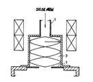
제1도는 종래의 ECR 플라즈마 장치의 구성을 설명하는데 사용되는 단면도이다. 마이크로 웨이브 발생기(도시되지 않음)에 의해 발생된 마이크로 웨이브는 도파관(1)을 통해 플라즈마 생성실(3)내로 인입된다. 플라즈마를 발생하는 N, O2, Ar 등과 같은 가스는 가스 공급 파이프(4)를 통해 플라즈마 생성실(3)내로 인입된다. 배기 시스템(도시되지 않음)에 의해 배기되는 플라즈마 생성실과, 대기압하에 있는 도파관(1)을 분리시키기 위해 석영같은 진공 윈도우(2)를 도파관(1)과 플라즈마 생성실(3) 사이에서 배치한다. 큰 개구(7A)를 갖는 금속판(7)은 플라즈마 생성실(3)의 하부 단부에 배치된다. 상기 금속판(7)과 플라즈마 생성실(3)은 반-개방된 마이크로 웨이브 공진기를 한정한다. ECR 상태를 만족시키기 적합한 자계가 발생되어 플라즈마가 공진실내에서 발생되는 방법으로 여자 솔레노이드(6)가 공진기의 외부 표면을 둘러싼다.1 is a cross-sectional view used to explain the configuration of a conventional ECR plasma apparatus. The microwaves generated by the microwave generator (not shown) are introduced into the
그에 따라 발생된 플라즈마는 자기력의 라인을 따라 처리실로 이동되어 기판 스탠드(10)로 향하게 된다. 예를들면, 모노실탄가스(SiH4)는 밸브(12A) 및 공급 파이프(12)를 포함하는 가스 공급 수단을 통해 처리실(9)로 인입되며, 상기 인입된 가스는 플라즈마에 의해 활성화된다. 활성화된 가스는 처리될 표본인 기판(11)에 반응하여, 박막이 기판 표면에 걸쳐 형성된다. 에칭 가스가 N2또는 그밖의 같은 종류 대신에 가스 공급 파이프(4)를 통해 제공될때, 상기 장치는 기판 표면을 에칭하는데 사용된다.The plasma generated thereby is moved to the process chamber along the line of magnetic force and directed to the
상기 기술된 형태의 ECR 플라즈마 에칭 장치 또는 CVD 장치의 구성과 동작에 기인한 문제점을 기술하기 전에, 플라즈마가 발생되는 방법을 기술하기로 한다. ECR 플라즈마 에칭 장치 또는 CVD 장치의 경우, 플라즈마 밀도를 증가시킴으로써 박막 성장 또는 효율적인 에칭을 수행하기 위해, ECR 상태를 만족시키는 자계 영역은 플라즈마 생성실내에서 설정되야 한다.Before describing the problems due to the construction and operation of an ECR plasma etching apparatus or CVD apparatus of the type described above, a method of generating plasma will be described. In the case of an ECR plasma etching apparatus or a CVD apparatus, in order to perform thin film growth or efficient etching by increasing the plasma density, a magnetic field region satisfying the ECR state must be set in the plasma generation chamber.
그러나, 여자 솔레노이드의 축방향 길이가 제한됨으로 솔레노이드의 길이가 축방향으로 제한받지 않을 경우 상기 자계 영역이 플라즈마 생성실의 전체 공간으로 확대 되는 것은 불가능하다. 상기 언급된 자계 영역은 단지 제한된 공간내에서만 존재하며, 플라즈마 생성실의 축 방향에서 영역의 위치는 외부 및 내부직경, 높이, 솔레노이드의 권선수 및, 여자 솔레노이드를 통해 흐르는 전류의 크기에 응답하여 결정된다.However, since the axial length of the excitation solenoid is limited, it is impossible to extend the magnetic field region to the entire space of the plasma generating chamber unless the length of the solenoid is limited in the axial direction. The above-mentioned magnetic field region exists only in a limited space, and the position of the region in the axial direction of the plasma generating chamber is determined in response to the outer and inner diameter, the height, the number of turns of the solenoid, and the magnitude of the current flowing through the excitation solenoid. do.
더욱이, 플라즈마의 발생량은 전계 강도와 자계 강도의 외적, 즉 E×B에 의존하기 때문에, 마이크로 웨이브 전계 강도 분포에 비례하는 자계영역(이하에서는 공진 자계 영역이라고 칭한다)은 중요한 인수로서, 기판면 처리속도와 처리된 면의 양호도, 예컨대 기판면상의 박막 성장속도, 성장 박막의 두께 분포 및 박막의 밀도에 영향을 준다. 플라즈마 생성실에서 마이크로 웨이브의 전계 강도 분포는 플라즈마 생성실의 형태와 규모 및 마이크로 웨이브와 로드와의 정합상태에 좌우된다. 제2도는 마이크로 웨이브의 전계 강도 분포를 도시한 것으로서, 이 분포도는 TE113공진 모드를 생성하는 공진기가 플라즈마 생성실을 구형할때이다. 이러한 경우, 플라즈마 생성실(3)내에서는 정상 마이크로 웨이브에 대해 세개의 첨두치가 있다. 플라즈마 생성실의 축방향에 대한 전계 강도는 정상파의 진폭과 같지만, 생성실로부터 방사선 방향으로 감에 따라 약해진다. 따라서, 솔레노이드에 흐르는 전류의 크기를 조정함으로서 공진 자계 영역이 생성된 공간이 제어 가능할 경우, 플라즈마 생성실의 ECR 플라즈마 발생 효율과 플라즈마의 밀도 분포를 조정하는 것이 가능하다고 생각된다.Furthermore, since the amount of plasma generated depends on the cross product of the electric field strength and the magnetic field strength, that is, E × B, a magnetic field region (hereinafter referred to as a resonant magnetic field region) proportional to the microwave electric field intensity distribution is an important factor. The speed and goodness of the treated face also affect the rate of thin film growth on the substrate surface, the thickness distribution of the growing thin film and the density of the thin film. The electric field intensity distribution of the microwaves in the plasma generating chamber depends on the shape and size of the plasma generating chamber and the matching state between the microwave and the rod. 2 shows the electric field intensity distribution of the microwaves, which is when the resonator generating the TE113 resonant mode is spherical in the plasma generating chamber. In this case, there are three peaks for the normal microwave in the
이상 설명한 기슐적인 요소만을 감안하면, 솔레노이드 전류만을 최적으로 조정하기만 하면 박막의 양, 박막 성장속도, 성장 박막 두께의 분포 등 전체적인 특성이 최적으로 되어야 하겠지만, 솔레노이드 전류의 제어만으로 해결할 수 없는 문제점이 있다.Considering only the elementary elements described above, if the solenoid current is adjusted only optimally, the overall characteristics such as the amount of the thin film, the growth rate of the thin film, and the distribution of the thickness of the growing thin film should be optimized. have.
이러한 관점에서, 본 발명의 목적은 전체적인 특성이 개량된 플라즈마 장치의 제공에 있다.In view of this, it is an object of the present invention to provide a plasma apparatus with improved overall characteristics.
또 다른 목적은 상기의 장치의 작동을 최상으로 하는 방법을 제공하는데 있다.Another object is to provide a method of optimizing the operation of the device.
본 발명의 장치의 첫번째 특징으로서, 플라즈마 처리 장치는, 마이크로 웨이브 발생 수단과, 상기 발생 수단에서 발생한 마이크로 웨이브를 전송하는 마이크로 웨이브 전송 수단과, 상기 마이크로 웨이브 전송수단과 통신하고, 가스 공급 수단 및 상기 전송 수단과 대향 관계에 있는 종단부에 설치된 개구를 갖는 플라즈마 생성실과, 상기 플라즈마 생성실 주위에 동축적으로 설치되고, 상기 마이크로 웨이브의 공진 효과로 플라즈마 생성실에 유입된 가스의 플라즈마를 발생하기 위해 자계를 제한시키는 여자 솔레노이드와, 상기 개구를 통해 플라즈마 생성실과 통신하고, 상기 플라즈마와 함께 그 내부에 설치된 기판면을 처리하는 처리실과, 상기 여기 솔레노이드의 위치를 플라즈마 생성실에 대해 축방향으로 변동시키는 변위 수단을 구비하고 있다.As a first feature of the apparatus of the present invention, a plasma processing apparatus includes: microwave generating means, microwave transmitting means for transmitting microwaves generated by the generating means, communicating with the microwave transmitting means, gas supply means and the A plasma generating chamber having an opening provided at an end portion opposed to the transmission means, and coaxially disposed around the plasma generating chamber, for generating plasma of a gas introduced into the plasma generating chamber by the resonance effect of the microwaves; An excitation solenoid for limiting a magnetic field, a processing chamber in communication with the plasma generation chamber through the opening, and processing a substrate surface provided therein with the plasma, and for varying the position of the excitation solenoid axially with respect to the plasma generation chamber. Displacement means is provided.
여기서, 영역의 위치, 즉 여자 솔레노이드에서 발생한 자계가 전자 사이클로트론 공진 조건을 충족하는 위치는, 플라즈마 생성실에 대한 여자 솔레노이드를 변위시킴으로서, 플라즈마 생성실내의 마이크로 웨이브 전계 강도에 비례하여 조정할 수 있다.Here, the position of the region, that is, the position where the magnetic field generated in the excitation solenoid satisfies the electron cyclotron resonance condition, can be adjusted in proportion to the intensity of the microwave field in the plasma generating chamber by displacing the excitation solenoid with respect to the plasma generating chamber.
여자 솔레노이드 전류의 크기는 가변 할 수 있다.The magnitude of the excitation solenoid current can vary.
처리실에는 가스 공급 수단이 설치되어 있다.The gas supply means is provided in the process chamber.
본 발명의 제2특징에 있어서는, 마이크로 웨이브와 자계간의 공진 효과로 플라즈마를 발생하기 위해 가스가 유입되는 플라즈마 생성실과, 플라즈마 생성실과 통신하는 처리실과, 상기 플라즈마 생성실 주위에 동축적으로 설치되고, 플라즈마 생성실에 대해 이동가능한 여자 솔레노이드를 구비한 플라즈마 처리 장치의 작동 방법에 있어서, 발생된 플라즈마의 밀도가 전류 크기의 증가에 따라 감소되는 범위로, 상기 여자 솔레노이드에 흐르는 전류의 크기를 정함으로서 플라즈마를 발생시키는 단계와, 상기 처리실 내부에서 놓인 시료를 처리하는 단계를 구비한다.According to a second aspect of the present invention, a plasma generation chamber into which gas is introduced to generate plasma by a resonance effect between microwaves and magnetic fields, a processing chamber communicating with the plasma generation chamber, and coaxially disposed around the plasma generation chamber, A method of operating a plasma processing apparatus having an excitation solenoid movable with respect to a plasma generating chamber, the method comprising: setting a magnitude of a current flowing through the excitation solenoid in a range in which the density of generated plasma decreases with an increase in current magnitude; Generating a; and processing a sample placed in the processing chamber.
이러한 방법에는 추가적으로, 상기 솔레노이드에 흐르는 전류의 크기를 변화시키는 단계와, 솔레노이드의 위치를 동축적으로 변화시키는 단계와, 상기 전류 크기 변화 단계, 솔레노이드 위치 변화 단계 및 시료처리 단계를 반복시키는 단계와, 상기 전류의 크기와 상기 솔레노이드의 위치를 결정하는 단계와, 상기 시료를 처리하는 단계를 구비할 수 있다.The method further includes changing the magnitude of the current flowing through the solenoid, changing the position of the solenoid coaxially, repeating the current magnitude changing step, the solenoid position changing step, and the sample processing step; Determining the magnitude of the current and the position of the solenoid; and processing the sample.
본 발명의 그밖의 목적, 효과 및 특징에 관하여는 첨부도면을 참조한 실시예의 설명을 통해서 분명해질 것이다.Other objects, effects, and features of the present invention will become apparent from the description of the embodiments with reference to the accompanying drawings.
본 발명자는 여자 솔레노이드를 통해 전류를 흘리므로써 플라즈마 생성실 안에서 발생된 자속 밀도의 분포에 대한 광대한 실험 및 상세한 분석을 이루었다. 산정된 결과가 제3도에 도시되는데, 여기서 해치 영역은 2.45GHz로 마이크로 웨이브와 공진하는 자속 밀도 875 가우스에 대한 자속의 에러가 ±1% 이내인 공진 자계 영역을 도시한다. 이 공진 자계 영역은 솔레노이드를 통해 흐르는 전류의 크기에 응답하여 변한다. ECR 상태가, 영역 A로 도시된 바와 같이, 세로 방향으로 솔레노이드의 중심부 근처에서 만족되는 방식으로 전류가 솔레노이드를 통해 흐르게 될때, 상기 공진 자계 영역은 축근처에서 솔레노이드의 축방향으로는 두껍지만 복사 방향으로는 그 두께가 갑자기 감소되어, 상기 플라즈마는 솔레노이드의 측 근처에 접속되는 경향이 있다. 한편, 공진 자계 영역이, 영역 B로 도시된 바와 같이 솔레노이드의 단부 근처에 발생되는 방식으로 전류가 솔레노이드를 통해 흐르게 될때, 공진 자계 영역의 두께는 솔레노이드의 축 근처에서는 얇지만 복사방향으로는 거의 일정하다. 영역 C는, 공진 자계 영역이 솔레노이드의 단부와 그것이 축 중심부 근처의 공간사이에 한정되는 방식으로 전류가 솔레노이드를 통해 흐를때의 공진 자계 영역을 도시해 준다. 이 명세서에 있어서, 영역 A로 한정된 자계에 의한 플라즈마 생성 모드는 모드 Ⅰ로 규정되고 영역 B로 한정된 자계에 의한 플라즈마 생성 모드는 모드 Ⅱ로 규정된다. 플라즈마가 모드 Ⅰ로 발생될때, 플라즈마 생성 능력은 높아져 비교적 고밀도를 가진 플라즈마가 얻어질 수 있다. 모드 Ⅱ의 경우, 플라즈마 생성 능력은 모드 Ⅰ보다 낮아지지만, 복사 방향으로의 플라즈마 밀도의 분포는 일정해진다. 제4도 및 5도는 N의 압력이 1mTorr, 흐름 속도가 30sccm이며 마이크로 웨이브의 파워가 400W인 조건하에서 플라즈마 생성실의 복사 방향으로 각각 모드 Ⅰ 및 Ⅱ에 의해 발생된 플라즈마의 밀도 분포를 나타낸다. 모드 Ⅰ에 있어서, 플라즈마 밀도내에서는 약 30%의 편차가 복사 방향으로 발생하지만, 모드 Ⅱ에 있어서는 약 10% 이내의 편차가 발생한다. 제4도 및 제5도에 있어서, 플라즈마 밀도는 상대적인 값으로 플로트되며, 이때 축에서의 밀도는 일정하지만 절대값은 모드 Ⅱ에서 보다 모드 Ⅰ에서 더 높다.The inventors have made extensive experiments and detailed analysis of the distribution of magnetic flux density generated in the plasma generating chamber by flowing a current through the excitation solenoid. The calculated results are shown in FIG. 3, where the hatch region shows a resonant magnetic field region with an error of magnetic flux within ± 1% for a magnetic flux density of 875 gauss that resonates with microwave at 2.45 GHz. This resonant magnetic field region changes in response to the magnitude of the current flowing through the solenoid. When the current flows through the solenoid in such a way that the ECR state is satisfied near the center of the solenoid in the longitudinal direction, as shown by region A, the resonant magnetic field region is thick in the axial direction of the solenoid near the axle but in the radiant direction. The thickness suddenly decreases so that the plasma tends to be connected near the side of the solenoid. On the other hand, when the resonant magnetic field region flows through the solenoid in a manner generated near the end of the solenoid as shown by region B, the thickness of the resonant magnetic field region is thin near the axis of the solenoid but almost constant in the radiation direction. Do. Region C shows the resonant magnetic field region when current flows through the solenoid in such a way that the resonant magnetic field region is defined between the end of the solenoid and the space near the center of the axis. In this specification, the plasma generation mode by the magnetic field defined by region A is defined as mode I and the plasma generation mode by the magnetic field defined by region B is defined as mode II. When the plasma is generated in mode I, the plasma generating capability is increased so that a plasma having a relatively high density can be obtained. In the mode II, the plasma generating capability is lower than the mode I, but the distribution of the plasma density in the radiation direction is constant. 4 and 5 show the density distribution of the plasma generated by the modes I and II in the radiation direction of the plasma generating chamber, respectively, under the condition that the pressure of N is 1 mTorr, the flow rate is 30 sccm, and the power of the microwave is 400W. In mode I, about 30% of the variation occurs in the radiation direction within the plasma density, while in mode II, about 10% of the variation occurs. In Figures 4 and 5, the plasma density is plotted relative, where the density at the axis is constant but the absolute value is higher in mode I than in mode II.
예를들면, 플라즈마 밀도가 커질때 기판의 표면에 대한 얇은 성장막은 보다 조밀해지지만, 플라즈마 밀도가 점점 작아질때는, 상기 막이 거칠어진다. 더욱이, 상기 박막 두께의 분포는 거의 플라즈마 밀도 분포와 비슷하다.For example, when the plasma density increases, the thin growth film on the surface of the substrate becomes denser, but when the plasma density becomes smaller, the film becomes rough. Moreover, the distribution of the thin film thickness is almost similar to the plasma density distribution.
제6A도 및 제6B도는, 예를들어, 모드(Ⅰ)에 따라 질소의 플라즈마가 발생되고, Si3N4박막이 기판의 표면을 통해 처리실로 실란(S1H4)을 도래시켜 성장될때 방사 방향으로 플라즈마 밀도와 박막 두께를 설명하는 도면이다. 제6A도 및 제6B도에 도시된 것처럼, 플라즈마 밀도의 분포와 박막 성장율의 분포, 즉, 성장된 박막의 두께 분포는 실제 상용 관계로 되어 있다. 따라서, 박막 특성 및 박막 성장율을 개선시키길 원할때는 그 박막을 모드(Ⅰ)에 따라 성장시키는 것이 바람직하며, 박막 두께의 분포를 개선시키길 원할때는 모드(Ⅱ)에 따라 그 박막을 성장시키는 것이 바람직하다. 박막 성장의 경우에, 원하는 박막의 특성과 성장된 박막의 두께 분포를 실제 얻을 수 있도록 장치를 동락시킬 수 있다.6A and 6B show, for example, when a plasma of nitrogen is generated in accordance with mode (I), and a Si3 N4 thin film is grown by bringing silane (S1 H4 ) through the surface of the substrate into the process chamber. It is a figure explaining plasma density and thin film thickness in a radial direction. As shown in Figs. 6A and 6B, the distribution of the plasma density and the distribution of the thin film growth rate, that is, the thickness distribution of the grown thin film, are in actual commercial relations. Therefore, when it is desired to improve thin film properties and thin film growth rate, it is desirable to grow the thin film according to mode (I), and when it is desired to improve the distribution of thin film thickness, it is preferable to grow the thin film according to mode (II). In the case of thin film growth, the device can be enclosed so that the desired thin film properties and the thickness distribution of the grown thin film can be obtained in practice.
제7도는 솔레노이드 전류에 따라 플라즈마 생성실에 발생된 플라즈마 밀도에 관계된 한 실시예를 설명한다.7 illustrates one embodiment related to the plasma density generated in the plasma generation chamber in accordance with the solenoid current.
이 경우에, 플라즈마 밀도는 솔레노이드 전류가 146A까지 상승할때까지 실제 불균일하게 된다. 그 솔레노이드 전류 크기의 범위는 플라즈마 발생기의 모드(Ⅰ)에 일치하고, 그 모드에 있어서, 플라즈마는 여자 솔레노이드의 축 방향으로 중앙 부근까지 발생된 공진 자계에 의해 발생된다. 그 솔레노이드 전류가 증가될때, 그 플라즈마 밀도는 급격히 강하한다.In this case, the plasma density is actually nonuniform until the solenoid current rises to 146A. The range of the solenoid current magnitude corresponds to the mode (I) of the plasma generator, in which the plasma is generated by the resonant magnetic field generated up to the center in the axial direction of the excitation solenoid. When the solenoid current is increased, the plasma density drops sharply.
플라즈마 밀도의 감소는 154A까지 솔레노이드 전류가 증가할때까지 계속되어, 솔레노이드 전류가 154A를 초과할때, 그 플라즈마 밀도는 다시 실제로 일정하게 된다. 그 플라즈마 밀도가 비교적 낮은 레벨에서 실제 유지될 수 있는 솔레노이드 전류 크기의 범위는 플라즈마 발생의 모드(Ⅱ)에 상응하는데, 그 모드에서 플라즈마는 여자 솔레노이드의 단부 근처에 발생된 공진 자계에 의해 발생된다. 모드(Ⅰ)에서 공진 자계 영역의 플라즈마 밀도는 한 숫자에 의해 모드(Ⅱ)에서의 것과 상이하게 된다. 그리고, 전이 영역이 존재하는데, 그 영역에서의 플라즈마 밀도는 솔레노이드 전류의 크기에 응답하여 변화한다.The decrease in plasma density continues until the solenoid current increases up to 154 A, so that when the solenoid current exceeds 154 A, the plasma density again becomes substantially constant again. The range of solenoid current magnitudes that can be actually maintained at a level at which the plasma density is relatively low corresponds to mode II of plasma generation, in which the plasma is generated by a resonant magnetic field generated near the end of the excitation solenoid. In mode (I), the plasma density of the resonant magnetic field region differs from that in mode (II) by one number. There is a transition region, where the plasma density changes in response to the magnitude of the solenoid current.
전이 영역과 모드(Ⅰ) 사이의 경계와, 전이 영역과 모드(Ⅱ) 사이의 경계에서 솔레노이드 전류의 크기는 여자 솔레노이드의 형태 및 크기와 플라즈마 생성실의 형태 및 크기에 따라 변화하지만, 제7도에 도시된 3영역은 장치의 각각의 치수와 관계없이 존재한다.The magnitude of the solenoid current at the boundary between the transition region and the mode (I) and at the boundary between the transition region and the mode (II) varies depending on the shape and size of the excitation solenoid and the shape and size of the plasma generating chamber. The three regions shown in are present irrespective of the respective dimensions of the device.
플라즈마 처리 장치를 동락시키는 종래의 방법에 따라, 공진 자계 영역은 솔레노이드 전류의 크기를 제어하여 전이 영역내의 적당한 위치에 지정되어, 한 박막이 성장된다.In accordance with the conventional method of colliding the plasma processing apparatus, the resonant magnetic field region is controlled at a proper position in the transition region by controlling the magnitude of the solenoid current, so that a thin film is grown.
그러나, 플라즈마 발생의 효과가 마이크로 웨이브 전계 세기의 분포 또는 특정 전계 세기의 위치에 관계된 공진 자계 영역의 위치에 큰 영향을 받기 때문에, 플라즈마 생성실에 관계된 여가 솔레노이드의 위치가 고정적으로 유지될때, 심지어 공진 자계 영역의 위치가 전이 영역내의 바람직한 위치에 있게 되고, 보다 최적 위치로 이동시키길 원할때, 전이 영역내의 공진 자계 영역을 변위시키는 것은 불가능하다. 반면에, 본 발명에 따른 플라즈마 처리 장치는 플라즈마 생성실에 관계되어 여자 솔레노이드의 위치가 이동 가능하게 설계 및 구성되어 있기 때문에, 솔레노이드 전류의 크기를 전이 영역에 상응하는 값으로 결정할 수 있고, 또한, 솔레노이드를 플라즈마 생성실의 축방향으로 이동시킬 수 있으며, 기판의 표면 처리에 대한 전체 특성을 보다 높은 레벨로 증가시킬 수 있다.However, since the effect of plasma generation is greatly influenced by the distribution of microwave field strength or the position of the resonant magnetic field relative to the position of a particular field intensity, even when the position of the leisure solenoid related to the plasma generating chamber is kept fixed, even resonance When the position of the magnetic field region is at the desired position in the transition region and it is desired to move to a more optimal position, it is impossible to displace the resonant magnetic field region in the transition region. On the other hand, since the plasma processing apparatus according to the present invention is designed and configured to move the position of the excitation solenoid in relation to the plasma generating chamber, the magnitude of the solenoid current can be determined as a value corresponding to the transition region. The solenoid can be moved in the axial direction of the plasma generation chamber and the overall properties of the substrate's surface treatment can be increased to a higher level.
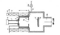
제8도는 본 발명에 따른 플라즈마 처리 장치의 한 실시예를 설명한다. 제1도와 제8도에 지정된 동일한 부분은 동일한 참고 부호를 이용하였다. 플라즈마 생성실(3)과 처리실(9)은 진공 시스템(도시하지 않음)에 의해 처리실(9)의 배기포트(9A)를 통해 높은 진공으로 상태를 유지하게 된다. 다음, Ar과 같은 결정된 기체가 기체 공급 파이프(4)를 통해 플라즈마 생성실(3)에 주입되는데, 그 내부 압력이 이미 결정된 레벨(예를들어, 1 내지 10mTorr)로 유지될 수 있도록 하여 주입된다.8 illustrates one embodiment of a plasma processing apparatus according to the present invention. Like parts designated in FIGS. 1 and 8 used the same reference numerals. The
마이크로 웨이브는 마이크로 웨이브 발진기, 아이소레이터 및 매칭 장치 등을 포함하는 마이크로 웨이브 발생 소스(13)로부터 파형안내(1)와 진공 윈도우(2)를 통해 플라즈마 생성실(3)로 주입되어, 그 전류는 여자 솔레노이드(14)를 통해 흐르게 되므로, ECR 상태를 만족시키는 자계가 공명기를 구성하는 플라즈마 생성실(3)에 발생되므로, 플라즈마를 발생시킨다.Microwaves are injected into the
동축으로 플라즈마 생성실(3)을 에워싸는 여자 솔레노이드(14)는 체인과 같은 구동력 전달 메카니즘(16)과 모터와 같은 구동원(15)에 의해서 수직으로 움직인다.The
솔레노이드(14)를 가이드하는 가이드 부재는 여자 솔레노이드(14) 부근에 배치된다. 체인 대신, 구동력 전달 메카니즘(16)은 기어, 나사 또는 다른 적절한 부재를 이용한다.The guide member for guiding the
가이드 부재 및 구동력 전달 메카니즘은 스테인레스 강철과 같은 비자성 재질로 이루어진다. 전류가 흐름으로서 솔레노이드(14)내에 발생한 공진 자계영역은 전술한 수직 리프팅 메카니즘에 의해서 플라즈마 생성실(3)의 축방향으로 넓은 범위에 걸쳐 놓여지며, 이는 솔레노이드의 축방향의 길이가 종래 여자 솔레노이드와 비교하여 짧아진 정도이며, 이에 의해서, 솔레노이드를 포함하는 장치의 주 몸체는 콤펙트한 크기의다.The guide member and drive force transmission mechanism are made of nonmagnetic material such as stainless steel. As the current flows, the resonant magnetic field generated in the
기판의 표면을 처리하는 경우, 여자 솔레노이드(14)는 소정 위치에 놓인다. 예를들면, 그 위치는 사실상 솔레노이드(14)의 축방향으로의 중심위치가 플라즈마 생성실(3)의 상단에 해당하게 결정된다. 그후, ECR 상태를 만족하는 자계가 발생될 수 있도록 솔레노이드를 통해 전류가 흐르도록 구성된다.When treating the surface of the substrate, the
이 경우, 프로브(probe) 방법과 같은 종래 방법에 의해서 전자 밀도를 검출하는 동안, 전류의 크기는 변화되며, 그 전류의 크기는 한 레벨에서 결정되는데, 이 레벨은 전류의 크기가 증가하는 동안 제7도에 도시한 바와 같이 플라즈마 밀도가 갑자기 감소되는 범위내이다. 이러한 전류의 크기는 모드 Ⅰ에 의해서 플라즈마가 생성되는 공진 자계 영역을 한정하는 전류의 크기가 모드 Ⅱ에 의해서 플라즈마가 생성되는 자계 영역을 한정하는 전류의 공진크기 사이에 존재한다. 한편, 전류의 크기는 전술한 전이 영역이 한정되는 정도의 크기이다. 다음, 여자 솔레노이드는 이 여자 솔레노이드(14)를 흐르는 전류의 크기가 처리시 박막품질, 이와 같이 성장한 막두께의 분포, 막성장을 등과 같은 전반적인 최적 특성을 얻을 수 있는 위치로 수직 이동되어 유지된다. 더 나아가, 전류의 크기는 전술한 전이 영역내에서 가변되며, 전술의 처리 단계는 표면처리가 보다 높은 레벨의 전반적인 특성에 도달하도록 수회 반복된다.In this case, during the detection of the electron density by a conventional method such as the probe method, the magnitude of the current is changed, and the magnitude of the current is determined at one level, which is determined while the magnitude of the current is increased. As shown in FIG. 7, the plasma density is in a range of sudden decrease. The magnitude of this current is between the resonance magnitude of the current defining the magnetic field region in which the plasma is generated by the mode I and the magnitude of the current defining the magnetic field region in which the plasma is generated by the Mode II. On the other hand, the magnitude of the current is such that the above-described transition region is limited. Next, the excitation solenoid is kept vertically moved to a position where the magnitude of the current flowing through the
솔레노이드 전류를 조절함으로써 소망 위치에서의 공진 자계 영역의 한정이 외곽 직경과 축방향의 전이 영역을 넓힌 솔레노이드의 두께를 증가함으로서 보다 안정한 방식으로 이루어짐을 알 수 있다.By adjusting the solenoid current, it can be seen that the limitation of the resonant magnetic field region at the desired position is achieved in a more stable manner by increasing the thickness of the solenoid which has widened the outer diameter and the axial transition region.
전술한 바와 같이, 본 발명에 따르면, 박막 성장율, 박막 품질, 박막 두께의 분포등과 같은 전반적인 특성이 보다 높은 레벨로 개선되며, 또한 에칭 처리의 경우, 전반적인 특성을 보다 높은 레벨로 끌어올릴 수 있는 표면처리를 실행하는 것이 가능하게 된다.As described above, according to the present invention, overall characteristics such as thin film growth rate, thin film quality, thin film thickness distribution, etc. are improved to a higher level, and in the case of etching treatment, the overall characteristics can be raised to a higher level. It is possible to perform the surface treatment.
본 발명이 바람직한 실시예와 관련하여 상세히 기술되었으며, 변화 및 수정은 광범위한 양상에서, 본 발명과 유리됨이 없이 행해질 수 있음은 본 발명이 속하는 분야에서의 통상의 숙련가들에게는 전술로부터 명백하며, 따라서 본 발명은 첨부된 특허청구 범위에서 발명의 진정한 사상과 일치하는 바와 같이 이러한 모든 변화 및 수정을 망라한다.The invention has been described in detail in connection with the preferred embodiments, and it is apparent from the foregoing to those skilled in the art that changes and modifications can be made in a wide variety of aspects without departing from the invention, and thus The invention encompasses all such changes and modifications as is consistent with the true spirit of the invention in the appended claims.
Claims (6)
Translated fromKoreanApplications Claiming Priority (2)
| Application Number | Priority Date | Filing Date | Title |
|---|---|---|---|
| JP60426 | 1990-03-12 | ||
| JP2060426AJP2546405B2 (en) | 1990-03-12 | 1990-03-12 | Plasma processing apparatus and operating method thereof |
Publications (1)
| Publication Number | Publication Date |
|---|---|
| KR0125448B1true KR0125448B1 (en) | 1997-12-26 |
Family
ID=13141886
Family Applications (1)
| Application Number | Title | Priority Date | Filing Date |
|---|---|---|---|
| KR1019910003821AExpired - Fee RelatedKR0125448B1 (en) | 1990-03-12 | 1991-03-11 | Plasma treatment apparatus and operation method thereof |
Country Status (5)
| Country | Link |
|---|---|
| US (1) | US5245157A (en) |
| JP (1) | JP2546405B2 (en) |
| KR (1) | KR0125448B1 (en) |
| DE (1) | DE4107753C2 (en) |
| GB (1) | GB2243944B (en) |
Families Citing this family (13)
| Publication number | Priority date | Publication date | Assignee | Title |
|---|---|---|---|---|
| JP3042127B2 (en)* | 1991-09-02 | 2000-05-15 | 富士電機株式会社 | Method and apparatus for manufacturing silicon oxide film |
| US5444207A (en)* | 1992-03-26 | 1995-08-22 | Kabushiki Kaisha Toshiba | Plasma generating device and surface processing device and method for processing wafers in a uniform magnetic field |
| US5660744A (en)* | 1992-03-26 | 1997-08-26 | Kabushiki Kaisha Toshiba | Plasma generating apparatus and surface processing apparatus |
| US5324388A (en)* | 1992-06-22 | 1994-06-28 | Matsushita Electric Industrial Co., Ltd. | Dry etching method and dry etching apparatus |
| JP3199957B2 (en)* | 1994-06-20 | 2001-08-20 | 株式会社日立製作所 | Microwave plasma processing method |
| US5733820A (en)* | 1995-04-27 | 1998-03-31 | Sharp Kabushiki Kaisha | Dry etching method |
| SG50732A1 (en)* | 1995-05-19 | 1998-07-20 | Hitachi Ltd | Method and apparatus for plasma processing apparatus |
| JPH11162958A (en)* | 1997-09-16 | 1999-06-18 | Tokyo Electron Ltd | Plasma processing apparatus and method |
| JP2000021871A (en)* | 1998-06-30 | 2000-01-21 | Tokyo Electron Ltd | Plasma processing method |
| DE10156615B4 (en)* | 2001-11-17 | 2004-10-07 | Forschungszentrum Karlsruhe Gmbh | Device for generating a locally variable electron cyclotron resonance microwave low pressure plasma |
| DE10341239B4 (en)* | 2003-09-08 | 2006-05-24 | Roth & Rau Ag | ECR plasma source with linear plasma outlet |
| CN106298425B (en)* | 2016-11-04 | 2017-09-29 | 大连理工大学 | Plasma Chambers for Improving Radial Uniformity of Plasma |
| CN111526653B (en)* | 2020-06-03 | 2024-04-26 | 吉林大学 | Microwave coupling plasma generating device with electromagnetic energy dual excitation function |
Family Cites Families (13)
| Publication number | Priority date | Publication date | Assignee | Title |
|---|---|---|---|---|
| CS176690B1 (en)* | 1975-03-04 | 1977-06-30 | ||
| CA1159012A (en)* | 1980-05-02 | 1983-12-20 | Seitaro Matsuo | Plasma deposition apparatus |
| JPS6037129A (en)* | 1983-08-10 | 1985-02-26 | Hitachi Ltd | Equipment for manufacturing semiconductor |
| DD217244A1 (en)* | 1983-08-31 | 1985-01-09 | Mikroelektronik Zt Forsch Tech | METHOD AND DEVICE FOR THE MAGNETIC SCRAPPING OF PLASMS |
| EP0273741B1 (en)* | 1986-12-29 | 1991-10-23 | Sumitomo Metal Industries, Ltd. | Plasma apparatus |
| DE3853890T2 (en)* | 1987-01-19 | 1995-10-19 | Hitachi Ltd | Device working with a plasma. |
| JPH0620048B2 (en)* | 1987-01-30 | 1994-03-16 | 富士電機株式会社 | Dry thin film processing equipment |
| US4778561A (en)* | 1987-10-30 | 1988-10-18 | Veeco Instruments, Inc. | Electron cyclotron resonance plasma source |
| DE3820237C1 (en)* | 1988-06-14 | 1989-09-14 | Max-Planck-Gesellschaft Zur Foerderung Der Wissenschaften Ev, 3400 Goettingen, De | |
| US4952273A (en)* | 1988-09-21 | 1990-08-28 | Microscience, Inc. | Plasma generation in electron cyclotron resonance |
| JP2913671B2 (en)* | 1989-06-29 | 1999-06-28 | ソニー株式会社 | ECR plasma CVD apparatus and method for manufacturing semiconductor device using the same |
| US5032202A (en)* | 1989-10-03 | 1991-07-16 | Martin Marietta Energy Systems, Inc. | Plasma generating apparatus for large area plasma processing |
| KR930004713B1 (en)* | 1990-06-18 | 1993-06-03 | 삼성전자 주식회사 | Plasma Generator and Method Using Modulation |
- 1990
- 1990-03-12JPJP2060426Apatent/JP2546405B2/ennot_activeExpired - Fee Related
- 1991
- 1991-03-11USUS07/666,522patent/US5245157A/ennot_activeExpired - Fee Related
- 1991-03-11KRKR1019910003821Apatent/KR0125448B1/ennot_activeExpired - Fee Related
- 1991-03-11DEDE4107753Apatent/DE4107753C2/ennot_activeExpired - Fee Related
- 1991-03-11GBGB9105063Apatent/GB2243944B/ennot_activeExpired - Fee Related
Also Published As
| Publication number | Publication date |
|---|---|
| JP2546405B2 (en) | 1996-10-23 |
| GB9105063D0 (en) | 1991-04-24 |
| GB2243944A (en) | 1991-11-13 |
| JPH03263799A (en) | 1991-11-25 |
| GB2243944B (en) | 1994-08-31 |
| US5245157A (en) | 1993-09-14 |
| DE4107753C2 (en) | 1998-03-19 |
| DE4107753A1 (en) | 1991-09-19 |
Similar Documents
| Publication | Publication Date | Title |
|---|---|---|
| US5785807A (en) | Microwave plasma processing method and apparatus | |
| KR0125448B1 (en) | Plasma treatment apparatus and operation method thereof | |
| US5556501A (en) | Silicon scavenger in an inductively coupled RF plasma reactor | |
| US6245190B1 (en) | Plasma processing system and plasma processing method | |
| US6068784A (en) | Process used in an RF coupled plasma reactor | |
| US5342472A (en) | Plasma processing apparatus | |
| US6251792B1 (en) | Plasma etch processes | |
| US6518195B1 (en) | Plasma reactor using inductive RF coupling, and processes | |
| US6545420B1 (en) | Plasma reactor using inductive RF coupling, and processes | |
| KR100255703B1 (en) | Plasma processor and method using electromagnetic RF connection | |
| EP0552491B1 (en) | Plasma etch process and plasma processing reactor | |
| US5888414A (en) | Plasma reactor and processes using RF inductive coupling and scavenger temperature control | |
| US6488807B1 (en) | Magnetic confinement in a plasma reactor having an RF bias electrode | |
| US5061838A (en) | Toroidal electron cyclotron resonance reactor | |
| US4970435A (en) | Plasma processing apparatus | |
| US5181986A (en) | Plasma processing apparatus | |
| US20020004309A1 (en) | Processes used in an inductively coupled plasma reactor | |
| EP0644575B1 (en) | Plasma generating method and apparatus and plasma processing method and apparatus | |
| US4915979A (en) | Semiconductor wafer treating device utilizing ECR plasma | |
| EP0228865A2 (en) | Magnetron-enhanced plasma etching process | |
| US6396024B1 (en) | Permanent magnet ECR plasma source with integrated multipolar magnetic confinement | |
| US5804033A (en) | Microwave plasma processing method and apparatus | |
| JP3973283B2 (en) | Plasma processing apparatus and plasma processing method | |
| RU2106716C1 (en) | Plant for microwave vacuum-plasma treatment of condensed media | |
| US5292395A (en) | ECR plasma reaction apparatus having uniform magnetic field gradient |
Legal Events
| Date | Code | Title | Description |
|---|---|---|---|
| PA0109 | Patent application | St.27 status event code:A-0-1-A10-A12-nap-PA0109 | |
| R17-X000 | Change to representative recorded | St.27 status event code:A-3-3-R10-R17-oth-X000 | |
| PG1501 | Laying open of application | St.27 status event code:A-1-1-Q10-Q12-nap-PG1501 | |
| A201 | Request for examination | ||
| P11-X000 | Amendment of application requested | St.27 status event code:A-2-2-P10-P11-nap-X000 | |
| P13-X000 | Application amended | St.27 status event code:A-2-2-P10-P13-nap-X000 | |
| PA0201 | Request for examination | St.27 status event code:A-1-2-D10-D11-exm-PA0201 | |
| G160 | Decision to publish patent application | ||
| E701 | Decision to grant or registration of patent right | ||
| PE0701 | Decision of registration | St.27 status event code:A-1-2-D10-D22-exm-PE0701 | |
| GRNT | Written decision to grant | ||
| PR0701 | Registration of establishment | St.27 status event code:A-2-4-F10-F11-exm-PR0701 | |
| PR1002 | Payment of registration fee | St.27 status event code:A-2-2-U10-U11-oth-PR1002 Fee payment year number:1 | |
| PG1601 | Publication of registration | St.27 status event code:A-4-4-Q10-Q13-nap-PG1601 | |
| R18-X000 | Changes to party contact information recorded | St.27 status event code:A-5-5-R10-R18-oth-X000 | |
| PR1001 | Payment of annual fee | St.27 status event code:A-4-4-U10-U11-oth-PR1001 Fee payment year number:4 | |
| PR1001 | Payment of annual fee | St.27 status event code:A-4-4-U10-U11-oth-PR1001 Fee payment year number:5 | |
| PR1001 | Payment of annual fee | St.27 status event code:A-4-4-U10-U11-oth-PR1001 Fee payment year number:6 | |
| FPAY | Annual fee payment | Payment date:20030924 Year of fee payment:7 | |
| PR1001 | Payment of annual fee | St.27 status event code:A-4-4-U10-U11-oth-PR1001 Fee payment year number:7 | |
| LAPS | Lapse due to unpaid annual fee | ||
| PC1903 | Unpaid annual fee | St.27 status event code:A-4-4-U10-U13-oth-PC1903 Not in force date:20041008 Payment event data comment text:Termination Category : DEFAULT_OF_REGISTRATION_FEE | |
| PC1903 | Unpaid annual fee | St.27 status event code:N-4-6-H10-H13-oth-PC1903 Ip right cessation event data comment text:Termination Category : DEFAULT_OF_REGISTRATION_FEE Not in force date:20041008 | |
| PN2301 | Change of applicant | St.27 status event code:A-5-5-R10-R13-asn-PN2301 St.27 status event code:A-5-5-R10-R11-asn-PN2301 | |
| PN2301 | Change of applicant | St.27 status event code:A-5-5-R10-R13-asn-PN2301 St.27 status event code:A-5-5-R10-R11-asn-PN2301 | |
| P22-X000 | Classification modified | St.27 status event code:A-4-4-P10-P22-nap-X000 |