JPWO2017221768A1 - Amplifier - Google Patents
AmplifierDownload PDFInfo
- Publication number
- JPWO2017221768A1 JPWO2017221768A1JP2018523931AJP2018523931AJPWO2017221768A1JP WO2017221768 A1JPWO2017221768 A1JP WO2017221768A1JP 2018523931 AJP2018523931 AJP 2018523931AJP 2018523931 AJP2018523931 AJP 2018523931AJP WO2017221768 A1JPWO2017221768 A1JP WO2017221768A1
- Authority
- JP
- Japan
- Prior art keywords
- voltage
- amplifier
- amplifiers
- signal
- power supply
- Prior art date
- Legal status (The legal status is an assumption and is not a legal conclusion. Google has not performed a legal analysis and makes no representation as to the accuracy of the status listed.)
- Pending
Links
- 230000003321amplificationEffects0.000claimsdescription23
- 238000003199nucleic acid amplification methodMethods0.000claimsdescription23
- 238000006243chemical reactionMethods0.000claimsdescription12
- 238000010586diagramMethods0.000description2
- 238000000034methodMethods0.000description2
- 238000012986modificationMethods0.000description2
- 230000004048modificationEffects0.000description2
- 238000012544monitoring processMethods0.000description2
- 239000004065semiconductorSubstances0.000description2
- 230000010355oscillationEffects0.000description1
- 239000007787solidSubstances0.000description1
- 238000006467substitution reactionMethods0.000description1
Images


Classifications
- H—ELECTRICITY
- H03—ELECTRONIC CIRCUITRY
- H03F—AMPLIFIERS
- H03F3/00—Amplifiers with only discharge tubes or only semiconductor devices as amplifying elements
- H03F3/20—Power amplifiers, e.g. Class B amplifiers, Class C amplifiers
- H03F3/21—Power amplifiers, e.g. Class B amplifiers, Class C amplifiers with semiconductor devices only
- H03F3/211—Power amplifiers, e.g. Class B amplifiers, Class C amplifiers with semiconductor devices only using a combination of several amplifiers
- H—ELECTRICITY
- H03—ELECTRONIC CIRCUITRY
- H03F—AMPLIFIERS
- H03F3/00—Amplifiers with only discharge tubes or only semiconductor devices as amplifying elements
- H03F3/20—Power amplifiers, e.g. Class B amplifiers, Class C amplifiers
- H03F3/24—Power amplifiers, e.g. Class B amplifiers, Class C amplifiers of transmitter output stages
- H—ELECTRICITY
- H03—ELECTRONIC CIRCUITRY
- H03F—AMPLIFIERS
- H03F1/00—Details of amplifiers with only discharge tubes, only semiconductor devices or only unspecified devices as amplifying elements
- H03F1/02—Modifications of amplifiers to raise the efficiency, e.g. gliding Class A stages, use of an auxiliary oscillation
- H03F1/0205—Modifications of amplifiers to raise the efficiency, e.g. gliding Class A stages, use of an auxiliary oscillation in transistor amplifiers
- H03F1/0211—Modifications of amplifiers to raise the efficiency, e.g. gliding Class A stages, use of an auxiliary oscillation in transistor amplifiers with control of the supply voltage or current
- H03F1/0216—Continuous control
- H03F1/0222—Continuous control by using a signal derived from the input signal
- H03F1/0227—Continuous control by using a signal derived from the input signal using supply converters
- H—ELECTRICITY
- H03—ELECTRONIC CIRCUITRY
- H03F—AMPLIFIERS
- H03F1/00—Details of amplifiers with only discharge tubes, only semiconductor devices or only unspecified devices as amplifying elements
- H03F1/02—Modifications of amplifiers to raise the efficiency, e.g. gliding Class A stages, use of an auxiliary oscillation
- H03F1/0205—Modifications of amplifiers to raise the efficiency, e.g. gliding Class A stages, use of an auxiliary oscillation in transistor amplifiers
- H03F1/0288—Modifications of amplifiers to raise the efficiency, e.g. gliding Class A stages, use of an auxiliary oscillation in transistor amplifiers using a main and one or several auxiliary peaking amplifiers whereby the load is connected to the main amplifier using an impedance inverter, e.g. Doherty amplifiers
- H—ELECTRICITY
- H03—ELECTRONIC CIRCUITRY
- H03F—AMPLIFIERS
- H03F3/00—Amplifiers with only discharge tubes or only semiconductor devices as amplifying elements
- H03F3/189—High-frequency amplifiers, e.g. radio frequency amplifiers
- H03F3/19—High-frequency amplifiers, e.g. radio frequency amplifiers with semiconductor devices only
- H03F3/195—High-frequency amplifiers, e.g. radio frequency amplifiers with semiconductor devices only in integrated circuits
- H—ELECTRICITY
- H03—ELECTRONIC CIRCUITRY
- H03F—AMPLIFIERS
- H03F3/00—Amplifiers with only discharge tubes or only semiconductor devices as amplifying elements
- H03F3/20—Power amplifiers, e.g. Class B amplifiers, Class C amplifiers
- H03F3/24—Power amplifiers, e.g. Class B amplifiers, Class C amplifiers of transmitter output stages
- H03F3/245—Power amplifiers, e.g. Class B amplifiers, Class C amplifiers of transmitter output stages with semiconductor devices only
- H—ELECTRICITY
- H03—ELECTRONIC CIRCUITRY
- H03F—AMPLIFIERS
- H03F3/00—Amplifiers with only discharge tubes or only semiconductor devices as amplifying elements
- H03F3/60—Amplifiers in which coupling networks have distributed constants, e.g. with waveguide resonators
- H03F3/602—Combinations of several amplifiers
- H—ELECTRICITY
- H03—ELECTRONIC CIRCUITRY
- H03F—AMPLIFIERS
- H03F3/00—Amplifiers with only discharge tubes or only semiconductor devices as amplifying elements
- H03F3/68—Combinations of amplifiers, e.g. multi-channel amplifiers for stereophonics
- H—ELECTRICITY
- H03—ELECTRONIC CIRCUITRY
- H03F—AMPLIFIERS
- H03F2200/00—Indexing scheme relating to amplifiers
- H03F2200/451—Indexing scheme relating to amplifiers the amplifier being a radio frequency amplifier
- H—ELECTRICITY
- H03—ELECTRONIC CIRCUITRY
- H03F—AMPLIFIERS
- H03F2203/00—Indexing scheme relating to amplifiers with only discharge tubes or only semiconductor devices as amplifying elements covered by H03F3/00
- H03F2203/20—Indexing scheme relating to power amplifiers, e.g. Class B amplifiers, Class C amplifiers
- H03F2203/21—Indexing scheme relating to power amplifiers, e.g. Class B amplifiers, Class C amplifiers with semiconductor devices only
- H03F2203/211—Indexing scheme relating to power amplifiers, e.g. Class B amplifiers, Class C amplifiers with semiconductor devices only using a combination of several amplifiers
- H03F2203/21106—An input signal being distributed in parallel over the inputs of a plurality of power amplifiers
- H—ELECTRICITY
- H03—ELECTRONIC CIRCUITRY
- H03F—AMPLIFIERS
- H03F2203/00—Indexing scheme relating to amplifiers with only discharge tubes or only semiconductor devices as amplifying elements covered by H03F3/00
- H03F2203/20—Indexing scheme relating to power amplifiers, e.g. Class B amplifiers, Class C amplifiers
- H03F2203/21—Indexing scheme relating to power amplifiers, e.g. Class B amplifiers, Class C amplifiers with semiconductor devices only
- H03F2203/211—Indexing scheme relating to power amplifiers, e.g. Class B amplifiers, Class C amplifiers with semiconductor devices only using a combination of several amplifiers
- H03F2203/21142—Output signals of a plurality of power amplifiers are parallel combined to a common output
Landscapes
- Engineering & Computer Science (AREA)
- Power Engineering (AREA)
- Microelectronics & Electronic Packaging (AREA)
- Amplifiers (AREA)
Abstract
Translated fromJapaneseDescription
Translated fromJapanese本発明は、RF信号を増幅する技術に関する。 The present invention relates to a technique for amplifying an RF signal.
近年、RF信号(Radio Frequency)の発振増幅素子としてのマグネトロン発振器による増幅機能の代替として、固体化電力増幅器(SSPA:Solid State Power Amplifier)を用いた増幅装置の需要が見込まれている。現行のマグネトロン発振器は、発振器と電源装置とが分離されており、これらの間が高い電圧により接続されている。そのため、マグネトロン発振器を上述の増幅装置で代替する場合には、同様に電源装置を分離することが望ましい。 In recent years, a demand for an amplification apparatus using a solid state power amplifier (SSPA) has been expected as an alternative to an amplification function by a magnetron oscillator as an oscillation amplification element of an RF signal (Radio Frequency). In the current magnetron oscillator, the oscillator and the power supply are separated, and they are connected by a high voltage. Therefore, when replacing the magnetron oscillator with the above-described amplification device, it is desirable to similarly separate the power supply device.
また、関連する技術として、電力出力段を含む高周波増幅手段と、電力出力段に給電するためのDC電圧の可変値を与える電力供給手段と、高周波増幅手段の入力電力の信号を制御入力として受信し、制御入力に応答してDC電圧の値を決定する制御信号を電力供給手段に与える制御手段を備える、アンテナの素子に給電するための半導体電力増幅器、が知られている(特許文献1参照)。 Further, as related techniques, high frequency amplification means including a power output stage, power supply means for giving a variable value of DC voltage for feeding power output stage, and a signal of input power of high frequency amplification means are received as control input A semiconductor power amplifier for feeding the elements of the antenna, comprising control means for providing the power supply means with a control signal for determining the value of the DC voltage in response to the control input (see Patent Document 1) ).
しかしながら、マグネトロン発振器の動作電圧が5kV程度であるのに対し、SSPAを用いた増幅装置は動作電圧が30V程度と低く、電力供給を同様とすると、増幅装置と電源装置とを低い電圧かつ大電流で接続することとなり、接続するケーブルを極端に太くしなければならない、ケーブルの長さが限定される、などの実用化を阻む制約が生じ、増幅装置と電源装置とを分離することが困難である、という問題がある。 However, while the operating voltage of the magnetron oscillator is about 5 kV, the amplifying device using SSPA has a low operating voltage of about 30 V, and the same power supply results in a low voltage and a large current between the amplifying device and the power supply device. It is difficult to separate the amplification device from the power supply device because the cables to be connected must be extremely thick and the length of the cable must be limited. There is a problem that there is.
本発明の実施形態は、上述した問題点を解決するためになされたものであり、より容易に電源装置と分離することができる増幅装置を提供することを目的とする。 The embodiments of the present invention are made to solve the above-described problems, and an object of the present invention is to provide an amplification device that can be easily separated from a power supply device.
上述した課題を解決するため、本実施形態の増幅装置は、外部機器から供給される供給電力の電圧をより低い電圧に変換する少なくとも1つ以上の電圧変換部と、前記少なくとも1つ以上の電圧変換部により電圧が変換された供給電力により動作し、高周波信号を増幅する少なくとも1つ以上の増幅器とを備える。 In order to solve the problems described above, the amplification device of the present embodiment includes at least one or more voltage conversion units for converting a voltage of supplied power supplied from an external device into a lower voltage, and the at least one or more voltages. The converter is provided with at least one or more amplifiers that operate with the supply power whose voltage has been converted by the conversion unit and that amplifies a high frequency signal.
本発明の実施形態によれば、より容易に電源部を分離することができる。 According to the embodiment of the present invention, the power supply unit can be more easily separated.
以下、図面を参照しながら、本発明の実施形態について説明する。 Hereinafter, embodiments of the present invention will be described with reference to the drawings.
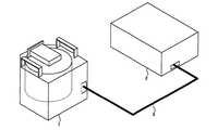
まず、本実施形態に係る増幅装置及び電源装置の概略について説明する。図1は、本実施形態に係る増幅装置及び電源装置を示す概略斜視図である。図2は、増幅装置の構成を示す概略図である。 First, an outline of the amplification device and the power supply device according to the present embodiment will be described. FIG. 1 is a schematic perspective view showing an amplification device and a power supply device according to the present embodiment. FIG. 2 is a schematic view showing the configuration of the amplification device.
図1に示すように、増幅装置1は、電源装置2と電源ケーブル3により接続されており、電源装置2は、電源ケーブル3を介して300V程度の比較的高い電圧で増幅装置1へ電源供給を行う。増幅装置1へ供給された電力の電圧は、増幅装置1内において30V程度に変換される。 As shown in FIG. 1, the amplification device 1 is connected to the power supply device 2 by the power supply cable 3, and the power supply device 2 supplies power to the amplification device 1 at a relatively high voltage of about 300 V via the power supply cable 3. I do. The voltage of the power supplied to the amplification device 1 is converted to about 30 V in the amplification device 1.
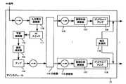
また、増幅装置1は、図2に示すように、入力されたRF信号を分配して出力するゲインモジュール11と、分配されて入力されたRF信号をそれぞれ増幅する複数の増幅器12と、複数の増幅器12それぞれにより増幅された複数のRF信号を合成して出力する合成器13と、合成器13により出力されたRF信号が入力される中空導波管14とを備える。 Further, as shown in FIG. 2, the amplification device 1 has a
次に、ゲインモジュールの構成及び増幅器の構成について説明する。図3は、ゲインモジュールの構成を示す図である。図4は、増幅器の構成を示す図である。 Next, the configuration of the gain module and the configuration of the amplifier will be described. FIG. 3 is a diagram showing the configuration of the gain module. FIG. 4 is a diagram showing the configuration of the amplifier.
図3に示すように、ゲインモジュール11は、入力電力監視部110、RFスイッチ111、可変減衰器112、固定減衰器113、アンプ114、分配器115、調整部116、電圧変換部119を備える。 As shown in FIG. 3, the
入力電力監視部110は、外部から入力されたRF信号の電力が適正かどうかを判定し、適正であればRF信号をRFスイッチ111へ出力する。RFスイッチ111は、外部機器からの制御に基づいてONまたはOFFに設定され、ONに設定された場合にのみ可変減衰器112へRF信号を出力する。可変減衰器112は、減衰量を可変に調整可能な減衰器であり、外部から入力される制御信号に基づいて、入力されたRF信号を減衰させて固定減衰器113へ出力する。固定減衰器113は、減衰量が固定された減衰器であり、入力されたRF信号を減衰させてアンプ114へ出力する。アンプ114は、入力されたRF信号を増幅して分配器115へ出力する。分配器115は、入力されたRF信号を分配して複数の調整部116のそれぞれに出力する。 The input
各調整部116は、振幅位相調整部117とプリドライバアンプ118とを有し、分配器115から出力されたRF信号の振幅及び位相を調整して対応する増幅器12へ出力する。振幅位相調整部117は、例えば、可変減衰器と移相器とにより構成され、入力されたRF信号の振幅と位相とを調整してプリドライバアンプ118へ出力する。プリドライバアンプ118は、入力されたRF信号を増幅して対応する増幅器12へ出力する。なお、各調整部116による振幅の調整量及び位相の調整量は個々に調整可能となっており、これらの調整量は例えば増幅装置1の出荷前に各調整部116から出力されるRF信号の振幅及び位相が互いに同等となるように調整される。 Each adjustment unit 116 includes an amplitude and
電圧変換部119は、電源ケーブル3を介して電源装置2により供給された電力の電圧を300Vから30Vに変換するDC/DCコンバータであり、30Vの直流電圧を各調整部116から各増幅器12への出力のそれぞれに重畳する。 The
図4に示すように、増幅器12は、半導体素子であるドライバアンプ120及びファイナルアンプ121と電圧変換部122とを備える。ドライバアンプ120は、増幅器12に入力されたRF信号を増幅してファイナルアンプ121へ出力する。ファイナルアンプ121は、ドライブアンプ120により出力されたRF信号を増幅して合成器13へ出力する。電圧変換部122は、電圧変換部119と同様に、電源ケーブル3を介して電源装置2により供給された電力の電圧を300Vから30Vに変換するDC/DCコンバータであり、30Vの電力をドライバアンプ120及びファイナルアンプ121へ供給する。増幅器12から出力されたRF信号は、合成器13によって合成されて中空導波管14へ出力される。 As shown in FIG. 4, the
上述したように、電源装置2から300V程度の比較的高い電圧かつ比較的小さい電流で供給される電力を増幅装置1内で30V程度の低い電圧に変換することによって、ケーブル3を太く短くすることなく、増幅装置1と電源装置2とを分離することができる。これによって、マグネトロン発振器が用いられる従来の構成に対する変更を少なくすることができ、延いては、マグネトロンをSSPAにより代替することがより容易とすることができる。 As described above, the cable 3 is made thick and short by converting the power supplied from the power supply device 2 with a relatively high voltage of about 300 V and a relatively small current into a low voltage of about 30 V in the amplification device 1 Instead, the amplification device 1 and the power supply device 2 can be separated. This makes it possible to reduce the changes to the conventional configuration in which the magnetron oscillator is used, which in turn makes it easier to replace the magnetron by SSPA.
本発明の実施形態は、例として提示したものであり、発明の範囲を限定することは意図していない。これら新規な実施形態は、その他の様々な形態で実施されることが可能であり、発明の要旨を逸脱しない範囲で、種々の省略、置き換え、変更を行うことができる。これら実施形態やその変形は、発明の範囲や要旨に含まれるとともに、特許請求の範囲に記載された発明とその均等の範囲に含まれる。 Embodiments of the present invention are presented as examples and are not intended to limit the scope of the invention. These novel embodiments can be implemented in various other forms, and various omissions, substitutions, and modifications can be made without departing from the scope of the invention. These embodiments and modifications thereof are included in the scope and the gist of the invention, and are included in the invention described in the claims and the equivalent scope thereof.
1 増幅装置、12 増幅器、13 合成器、115 分配器、119 電圧変換部、122 電圧変換部。1 amplifier, 12 amplifiers, 13 combiners, 115 dividers, 119 voltage converters, 122 voltage converters.
Claims (4)
Translated fromJapanese前記少なくとも1つ以上の電圧変換部により電圧が変換された供給電力により動作し、高周波信号を増幅する少なくとも1つ以上の増幅器と
を備える増幅装置。At least one or more voltage conversion units for converting the voltage of the supplied power supplied from the external device into a lower voltage;
An amplification device comprising: at least one or more amplifiers that operate with supplied power whose voltage has been converted by the at least one or more voltage conversion units and that amplifies high frequency signals.
入力された高周波信号を分配して前記複数の増幅器へ出力する分配器を更に備え、
前記複数の電圧変換部のうち1つは、前記分配器から前記複数の増幅器への出力に電圧を重畳することを特徴とする請求項1または請求項2に記載の増幅装置。The at least one or more amplifiers and the at least one or more voltage conversion units are plural,
It further comprises a divider for distributing the input high frequency signal and outputting it to the plurality of amplifiers,
The amplification device according to claim 1, wherein one of the plurality of voltage conversion units superposes a voltage on an output from the divider to the plurality of amplifiers.
Applications Claiming Priority (3)
| Application Number | Priority Date | Filing Date | Title |
|---|---|---|---|
| JP2016125238 | 2016-06-24 | ||
| JP2016125238 | 2016-06-24 | ||
| PCT/JP2017/021822WO2017221768A1 (en) | 2016-06-24 | 2017-06-13 | Amplification device |
Publications (1)
| Publication Number | Publication Date |
|---|---|
| JPWO2017221768A1true JPWO2017221768A1 (en) | 2019-04-18 |
Family
ID=60783954
Family Applications (1)
| Application Number | Title | Priority Date | Filing Date |
|---|---|---|---|
| JP2018523931APendingJPWO2017221768A1 (en) | 2016-06-24 | 2017-06-13 | Amplifier |
Country Status (6)
| Country | Link |
|---|---|
| US (1) | US10840859B2 (en) |
| JP (1) | JPWO2017221768A1 (en) |
| KR (1) | KR20190020651A (en) |
| CN (1) | CN109314495A (en) |
| TW (1) | TWI727034B (en) |
| WO (1) | WO2017221768A1 (en) |
Families Citing this family (1)
| Publication number | Priority date | Publication date | Assignee | Title |
|---|---|---|---|---|
| KR102377839B1 (en)* | 2019-10-25 | 2022-03-23 | 큐알티 주식회사 | High frequency enhancing apparatus |
Citations (11)
| Publication number | Priority date | Publication date | Assignee | Title |
|---|---|---|---|---|
| JPS57200937U (en)* | 1981-06-17 | 1982-12-21 | ||
| JPS63131624A (en)* | 1986-11-20 | 1988-06-03 | Nec Corp | Transistor equipment |
| JPH0492833U (en)* | 1990-12-29 | 1992-08-12 | ||
| JPH06164269A (en)* | 1992-11-26 | 1994-06-10 | Mitsubishi Electric Corp | Power amplifier |
| JPH07212255A (en)* | 1994-01-21 | 1995-08-11 | Kokusai Electric Co Ltd | Transmission output control circuit and transmission output control method |
| JPH11340755A (en)* | 1998-05-27 | 1999-12-10 | Mitsubishi Electric Corp | Microwave module |
| JP2001177423A (en)* | 1999-12-16 | 2001-06-29 | Nec Network Sensa Kk | Tdma system digital wireless transmitter |
| JP2001185967A (en)* | 1999-12-27 | 2001-07-06 | Matsushita Electric Ind Co Ltd | High frequency power amplifier |
| JP2003516690A (en)* | 1999-12-10 | 2003-05-13 | モトローラ・インコーポレイテッド | Power amplification core |
| JP2012199746A (en)* | 2011-03-22 | 2012-10-18 | Nec Corp | Doherty amplifier and bias setting method for doherty amplifier |
| WO2014155512A1 (en)* | 2013-03-26 | 2014-10-02 | 日本電気株式会社 | Power amplifier |
Family Cites Families (16)
| Publication number | Priority date | Publication date | Assignee | Title |
|---|---|---|---|---|
| US5491454A (en)* | 1994-10-31 | 1996-02-13 | Motorola, Inc. | Method and apparatus for reducing distortion in an output signal of an amplifier |
| US6603391B1 (en)* | 1999-03-09 | 2003-08-05 | Micron Technology, Inc. | Phase shifters, interrogators, methods of shifting a phase angle of a signal, and methods of operating an interrogator |
| EP1267487A1 (en)* | 2001-06-15 | 2002-12-18 | Contraves Space AG | High frequency amplifier |
| US6985039B2 (en)* | 2003-04-25 | 2006-01-10 | Paragon Communications Ltd. | Method and apparatus for providing a stable power output of power amplifiers, operating under unstable supply voltage conditions |
| JP4440121B2 (en)* | 2005-01-06 | 2010-03-24 | Necエレクトロニクス株式会社 | Voltage supply circuit and microphone unit |
| RU2434317C2 (en) | 2006-05-05 | 2011-11-20 | Астриум Лимитед | Radio-frequency power amplifiers |
| CN100582801C (en)* | 2007-11-29 | 2010-01-20 | 中兴通讯股份有限公司 | Batch detector methods and apparatus of power amplifier |
| WO2009147891A1 (en)* | 2008-06-02 | 2009-12-10 | 株式会社 東芝 | Wireless transmission device using cartesian loop |
| JP2010154460A (en)* | 2008-12-26 | 2010-07-08 | Hitachi Kokusai Electric Inc | High-frequency power amplifying device |
| US8542061B2 (en)* | 2010-04-20 | 2013-09-24 | Rf Micro Devices, Inc. | Charge pump based power amplifier envelope power supply and bias power supply |
| EP2432118B1 (en)* | 2010-09-15 | 2012-12-26 | Agence Spatiale Européenne | Radio-frequency power amplifier with fast envelope tracking |
| US20150244334A1 (en)* | 2012-09-26 | 2015-08-27 | Sharp Kabushiki Kaisha | Amplification device and radio communication apparatus equipped with amplification device |
| US8884696B2 (en)* | 2012-10-15 | 2014-11-11 | Intel Mobile Communications GmbH | Control circuit and method for controlling an operation of a power amplifier |
| JP5933471B2 (en)* | 2013-03-14 | 2016-06-08 | パナソニック株式会社 | Phased array transmitter |
| DE102014104364A1 (en) | 2014-03-28 | 2015-10-01 | Intel IP Corporation | An apparatus and method for providing a supply control signal to a supply unit |
| JP2016119609A (en)* | 2014-12-22 | 2016-06-30 | 富士通株式会社 | Amplification device |
- 2017
- 2017-04-19TWTW106113050Apatent/TWI727034B/enactive
- 2017-06-13USUS16/098,745patent/US10840859B2/enactiveActive
- 2017-06-13KRKR1020187033053Apatent/KR20190020651A/ennot_activeCeased
- 2017-06-13JPJP2018523931Apatent/JPWO2017221768A1/enactivePending
- 2017-06-13CNCN201780038551.9Apatent/CN109314495A/enactivePending
- 2017-06-13WOPCT/JP2017/021822patent/WO2017221768A1/ennot_activeCeased
Patent Citations (11)
| Publication number | Priority date | Publication date | Assignee | Title |
|---|---|---|---|---|
| JPS57200937U (en)* | 1981-06-17 | 1982-12-21 | ||
| JPS63131624A (en)* | 1986-11-20 | 1988-06-03 | Nec Corp | Transistor equipment |
| JPH0492833U (en)* | 1990-12-29 | 1992-08-12 | ||
| JPH06164269A (en)* | 1992-11-26 | 1994-06-10 | Mitsubishi Electric Corp | Power amplifier |
| JPH07212255A (en)* | 1994-01-21 | 1995-08-11 | Kokusai Electric Co Ltd | Transmission output control circuit and transmission output control method |
| JPH11340755A (en)* | 1998-05-27 | 1999-12-10 | Mitsubishi Electric Corp | Microwave module |
| JP2003516690A (en)* | 1999-12-10 | 2003-05-13 | モトローラ・インコーポレイテッド | Power amplification core |
| JP2001177423A (en)* | 1999-12-16 | 2001-06-29 | Nec Network Sensa Kk | Tdma system digital wireless transmitter |
| JP2001185967A (en)* | 1999-12-27 | 2001-07-06 | Matsushita Electric Ind Co Ltd | High frequency power amplifier |
| JP2012199746A (en)* | 2011-03-22 | 2012-10-18 | Nec Corp | Doherty amplifier and bias setting method for doherty amplifier |
| WO2014155512A1 (en)* | 2013-03-26 | 2014-10-02 | 日本電気株式会社 | Power amplifier |
Also Published As
| Publication number | Publication date |
|---|---|
| US20190140604A1 (en) | 2019-05-09 |
| US10840859B2 (en) | 2020-11-17 |
| TWI727034B (en) | 2021-05-11 |
| WO2017221768A1 (en) | 2017-12-28 |
| CN109314495A (en) | 2019-02-05 |
| KR20190020651A (en) | 2019-03-04 |
| TW201801471A (en) | 2018-01-01 |
Similar Documents
| Publication | Publication Date | Title |
|---|---|---|
| US9438187B2 (en) | Amplifying device, transmitting device | |
| EP3089359A1 (en) | Power amplifying apparatus and method for controlling power amplifying apparatus | |
| JPWO2017221768A1 (en) | Amplifier | |
| US20160204743A1 (en) | Power amplification apparatus and control method of power amplification apparatus | |
| JP2020156024A (en) | Amplifier | |
| JP2016171500A (en) | Power amplification device and control method of power amplification device | |
| JP6267765B2 (en) | Power supply stage and method for generating output supply signal | |
| JP2011211655A (en) | High frequency amplifier | |
| JP6183453B2 (en) | Power amplification device and power amplification method | |
| JP2015033083A (en) | Multiband amplifier | |
| CN102545801A (en) | Transmitting device | |
| JP7281932B2 (en) | amplifier | |
| JP3598991B2 (en) | Configuration method of low distortion power amplifier circuit | |
| JP2024101700A (en) | Power amplifier for digital broadcasting and digital broadcasting transmission device | |
| JP5010542B2 (en) | High frequency power amplifier and amplification method | |
| JP2006135528A (en) | Power amplifier and power amplification method | |
| JP2011040956A (en) | Radio transmitter | |
| WO2016130785A1 (en) | Switcher noise reduction | |
| JP2013126081A (en) | Digital amplitude modulation device and method of controlling the same |
Legal Events
| Date | Code | Title | Description |
|---|---|---|---|
| A621 | Written request for application examination | Free format text:JAPANESE INTERMEDIATE CODE: A621 Effective date:20190107 | |
| A131 | Notification of reasons for refusal | Free format text:JAPANESE INTERMEDIATE CODE: A131 Effective date:20191203 | |
| A521 | Request for written amendment filed | Free format text:JAPANESE INTERMEDIATE CODE: A523 Effective date:20200127 | |
| A131 | Notification of reasons for refusal | Free format text:JAPANESE INTERMEDIATE CODE: A131 Effective date:20200512 | |
| A521 | Request for written amendment filed | Free format text:JAPANESE INTERMEDIATE CODE: A523 Effective date:20200612 | |
| A02 | Decision of refusal | Free format text:JAPANESE INTERMEDIATE CODE: A02 Effective date:20200915 |