JPWO2016125261A1 - Laminated molded body and laminated light emitting body - Google Patents
Laminated molded body and laminated light emitting bodyDownload PDFInfo
- Publication number
- JPWO2016125261A1 JPWO2016125261A1JP2016572987AJP2016572987AJPWO2016125261A1JP WO2016125261 A1JPWO2016125261 A1JP WO2016125261A1JP 2016572987 AJP2016572987 AJP 2016572987AJP 2016572987 AJP2016572987 AJP 2016572987AJP WO2016125261 A1JPWO2016125261 A1JP WO2016125261A1
- Authority
- JP
- Japan
- Prior art keywords
- circuit board
- electronic circuit
- carbon fiber
- fiber reinforced
- reinforced plastic
- Prior art date
- Legal status (The legal status is an assumption and is not a legal conclusion. Google has not performed a legal analysis and makes no representation as to the accuracy of the status listed.)
- Granted
Links
Images


Classifications
- H—ELECTRICITY
- H05—ELECTRIC TECHNIQUES NOT OTHERWISE PROVIDED FOR
- H05K—PRINTED CIRCUITS; CASINGS OR CONSTRUCTIONAL DETAILS OF ELECTRIC APPARATUS; MANUFACTURE OF ASSEMBLAGES OF ELECTRICAL COMPONENTS
- H05K1/00—Printed circuits
- H05K1/02—Details
- H—ELECTRICITY
- H05—ELECTRIC TECHNIQUES NOT OTHERWISE PROVIDED FOR
- H05K—PRINTED CIRCUITS; CASINGS OR CONSTRUCTIONAL DETAILS OF ELECTRIC APPARATUS; MANUFACTURE OF ASSEMBLAGES OF ELECTRICAL COMPONENTS
- H05K1/00—Printed circuits
- H05K1/18—Printed circuits structurally associated with non-printed electric components
Landscapes
- Engineering & Computer Science (AREA)
- Microelectronics & Electronic Packaging (AREA)
- Led Device Packages (AREA)
- Fastening Of Light Sources Or Lamp Holders (AREA)
- Structure Of Printed Boards (AREA)
Abstract
Translated fromJapaneseDescription
Translated fromJapanese本願発明は、電子回路基板の表裏面を炭素繊維強化プラスチック(CFRP:Carbon Fiber Reinforced Plastics)で挟み込んで接着し一体化した積層成形体に関するものである。 The present invention relates to a laminated molded body in which the front and back surfaces of an electronic circuit board are sandwiched and bonded by carbon fiber reinforced plastics (CFRP: Carbon Fiber Reinforced Plastics).
電子回路基板と前記電子回路基板を保護する保護筐体からなる電子回路基板内蔵ユニット(電子回路基板部品・製品などともいう。)は、従来から存在する(例えば、特許文献1のプリント板ユニット)。 An electronic circuit board built-in unit (also referred to as an electronic circuit board component / product) that includes an electronic circuit board and a protective housing that protects the electronic circuit board has conventionally existed (for example, a printed board unit of Patent Document 1). .
前述したような電子回路基板内蔵ユニットは、保護筐体の内部へ電子回路基板を組み込むための組立工程が介在し、組立工程が介在することにより、以下の課題が存在してしまう。 An electronic circuit board built-in unit as described above involves an assembly process for assembling an electronic circuit board inside the protective housing, and the following problems exist due to the assembly process.
組立作業や品質管理のためのコストが必要となる。 Costs for assembly work and quality control are required.
生産タクトの安定化が難しく、製品のリードタイムが長くなる。作業者のスキルが技能力に依存するためである。 Stabilization of production tact is difficult and product lead time becomes longer. This is because the skill of the worker depends on the skill.
品質の安定化が難しくなる。作業者のスキルが技能力に依存するためである。 It becomes difficult to stabilize the quality. This is because the skill of the worker depends on the skill.
作業はマニュアル化できても、コアになる製造・生産技術の維持・伝承に負担がかかる。作業者のスキルが技能力に依存するためである。 Even if the work can be manualized, it takes a burden to maintain and pass down core manufacturing and production technologies. This is because the skill of the worker depends on the skill.
個々の電気回路モジュールや電子・電機部品を固定・保持するために必要な追加構造や構造部品が必要となり、製品の構造が複雑になる。 Additional structures and structural parts necessary for fixing and holding individual electric circuit modules and electronic / electrical parts are required, which complicates the structure of the product.
そこで、電子回路基板を内蔵しながら構造物との一体化を図ることで、既存の組立品を置き換えられる積層成形体を提供することを課題とした。 Therefore, an object of the present invention is to provide a laminated molded body that can replace an existing assembly by integrating with a structure while incorporating an electronic circuit board.
本願発明の積層成形体は、上述の課題を解決するために、所定の部品を表面側または裏面側の少なくとも一方に固着実装した所定形状の電子回路基板と、前記電子回路基板の表面側に積層して設ける第一炭素繊維強化プラスチック体と、前記電子回路基板の裏面側に積層して設ける第二炭素繊維強化プラスチック体と、前記電子回路基板のうち前記所定の部品を固着実装した側の面と前記第一炭素繊維強化プラスチック体又は前記第二炭素繊維強化プラスチック体との間に挟設する絶縁層と、からなり、前記電子回路基板、前記絶縁層、前記第一炭素繊維強化プラスチック体及び前記第二炭素繊維強化プラスチック体を接着により一体化した積層成形体を提供する。 In order to solve the above-described problems, the laminated molded body of the present invention is a laminated electronic circuit board having a predetermined shape in which a predetermined part is fixedly mounted on at least one of the front side and the back side, and the front side of the electronic circuit board. A first carbon fiber reinforced plastic body provided, a second carbon fiber reinforced plastic body provided by being laminated on the back side of the electronic circuit board, and a surface of the electronic circuit board on which the predetermined component is fixedly mounted. And an insulating layer interposed between the first carbon fiber reinforced plastic body or the second carbon fiber reinforced plastic body, and the electronic circuit board, the insulating layer, the first carbon fiber reinforced plastic body, and Provided is a laminated molded body in which the second carbon fiber reinforced plastic body is integrated by adhesion.
また、本願発明の積層発光体は、上述の課題を解決するために、所定の部品を表面側または裏面側の少なくとも一方に固着実装した所定形状の電子回路基板と、前記電子回路基板の表面側に積層して設ける第一炭素繊維強化プラスチック体と、前記電子回路基板の裏面側に積層して設け前記第一炭素繊維強化プラスチック体と厚さが同一である第二炭素繊維強化プラスチック体と、前記電子回路基板のうち前記所定の部品を固着実装した側の面と前記第一炭素繊維強化プラスチック体又は前記第二炭素繊維強化プラスチック体との間に挟設する絶縁層と、からなり、前記電子回路基板、前記絶縁層、前記第一炭素繊維強化プラスチック体及び前記第二炭素繊維強化プラスチック体を接着により一体化した積層成形体を提供する。 In addition, in order to solve the above-described problems, the multilayer light emitting device of the present invention includes an electronic circuit board having a predetermined shape in which predetermined components are fixedly mounted on at least one of the front side and the back side, and the front side of the electronic circuit board. A first carbon fiber reinforced plastic body provided by laminating, and a second carbon fiber reinforced plastic body having the same thickness as the first carbon fiber reinforced plastic body provided by laminating on the back side of the electronic circuit board, An insulating layer sandwiched between a surface of the electronic circuit board on which the predetermined component is fixedly mounted and the first carbon fiber reinforced plastic body or the second carbon fiber reinforced plastic body, and Provided is a laminated molded body in which an electronic circuit board, the insulating layer, the first carbon fiber reinforced plastic body, and the second carbon fiber reinforced plastic body are integrated by bonding.
また、本願発明の積層成形体は、上述の課題を解決するために、所定の部品を表面側または裏面側の少なくとも一方に固着実装した断面台形形状又は断面波形状の電子回路基板と、前記電子回路基板の表面側に積層して設ける第一炭素繊維強化プラスチック体と、前記電子回路基板の裏面側に積層して設ける第二炭素繊維強化プラスチック体と、前記電子回路基板のうち前記所定の部品を固着実装した側の面と前記第一炭素繊維強化プラスチック体又は前記第二炭素繊維強化プラスチック体との間に挟設する絶縁層と、からなり、前記電子回路基板、前記絶縁層、前記第一炭素繊維強化プラスチック体及び前記第二炭素繊維強化プラスチック体を接着により一体化した積層成形体を提供する。 In order to solve the above-described problems, the laminated molded body of the present invention includes a cross-sectional trapezoidal or cross-sectional electronic circuit board in which a predetermined component is fixedly mounted on at least one of the front side and the back side, and the electronic A first carbon fiber reinforced plastic body provided by being laminated on the front side of the circuit board; a second carbon fiber reinforced plastic body provided by being laminated on the back side of the electronic circuit board; and the predetermined component of the electronic circuit board And an insulating layer sandwiched between the first carbon fiber reinforced plastic body or the second carbon fiber reinforced plastic body, and the electronic circuit board, the insulating layer, and the first carbon fiber reinforced plastic body. Provided is a laminated molded body in which one carbon fiber reinforced plastic body and the second carbon fiber reinforced plastic body are integrated by adhesion.
また、本願発明の積層発光体は、上述の課題を解決するために、所定の部品(少なくとも発光する部品を包含する)を表面側または裏面側の少なくとも一方に固着実装した所定形状の電子回路基板と、前記電子回路基板の表面側に積層して設ける第一炭素繊維強化プラスチック体と、前記電子回路基板の裏面側に積層して設ける第二炭素繊維強化プラスチック体と、前記電子回路基板のうち前記所定の部品を固着実装した側の面と前記第一炭素繊維強化プラスチック体又は前記第二炭素繊維強化プラスチック体との間に挟設する絶縁層と、からなり、前記電子回路基板、前記絶縁層、前記第一炭素繊維強化プラスチック体及び前記第二炭素繊維強化プラスチック体を接着により一体化しするとともに、前記第一炭素繊維強化プラスチック体又は前記第二炭素繊維強化プラスチック体の表面側から前記発光する部品の先端部が、突出しない積層発光体を提供する。 In addition, in order to solve the above-described problems, the multilayer light emitting device of the present invention is a predetermined-shaped electronic circuit board in which predetermined components (including at least a component that emits light) are fixedly mounted on at least one of the front surface side and the rear surface side. A first carbon fiber reinforced plastic body provided on the front side of the electronic circuit board, a second carbon fiber reinforced plastic body provided on the back side of the electronic circuit board, and the electronic circuit board. The electronic circuit board, the insulation Layer, the first carbon fiber reinforced plastic body and the second carbon fiber reinforced plastic body are integrated by bonding, and the first carbon fiber reinforced plastic body or Tip of the part for the emission from the surface of the second carbon fiber reinforced plastic body, to provide a laminated illuminant does not protrude.
また、本願発明の積層発光体は、上述の課題を解決するために、所定の部品(少なくとも発光する部品を包含する)を表面側または裏面側の少なくとも一方に固着実装した所定形状の電子回路基板と、前記電子回路基板の表面側に積層して設ける第一炭素繊維強化プラスチック体と、前記電子回路基板の裏面側に積層して設ける第二炭素繊維強化プラスチック体と、前記電子回路基板のうち前記所定の部品を固着した側の面と前記第一炭素繊維強化プラスチック体又は前記第二炭素繊維強化プラスチック体との間に挟設する絶縁層と、からなり、前記電子回路基板、前記絶縁層、前記第一炭素繊維強化プラスチック体及び前記第二炭素繊維強化プラスチック体を接着により一体化しするとともに、前記第一炭素繊維強化プラスチック体又は前記第二炭素繊維強化プラスチック体の表面側から前記発光する部品の先端部が、突出する積層発光体を提供する。 In addition, in order to solve the above-described problems, the multilayer light emitting device of the present invention is a predetermined-shaped electronic circuit board in which predetermined components (including at least a component that emits light) are fixedly mounted on at least one of the front surface side and the rear surface side. A first carbon fiber reinforced plastic body provided on the front side of the electronic circuit board, a second carbon fiber reinforced plastic body provided on the back side of the electronic circuit board, and the electronic circuit board. An insulating layer sandwiched between a surface on which the predetermined component is fixed and the first carbon fiber reinforced plastic body or the second carbon fiber reinforced plastic body, and the electronic circuit board and the insulating layer The first carbon fiber reinforced plastic body and the second carbon fiber reinforced plastic body are integrated by bonding, and the first carbon fiber reinforced plastic body or the front Tip of the part for the emission from the surface of the second carbon fiber reinforced plastic body, to provide a laminated illuminant projecting.
本願発明の積層成形体は、電子回路基板と前記電子回路基板の保護部材をあらかじめ一体成形しているため、保護筐体の内部へ電子回路基板を組み込むための組立工程が介在せず、組立作業や品質管理分のコストが低減できる。また、生産タクトも安定し、リードタイム短縮にも貢献できる。品質の安定化が容易となる。コアになる製造・生産技術の維持・伝承に負担が軽減される。構造上の簡素化を図ることができる。軽量かつ高強度になる等の効果も生じる。なお、炭素繊維の熱伝動性はアルミ等の金属よりも優れているので発熱する電子部品の発熱効果も期待できる。 In the laminated molded body of the present invention, since the electronic circuit board and the protective member for the electronic circuit board are integrally formed in advance, an assembly process for assembling the electronic circuit board into the protective housing is not involved, and assembly work is performed. And cost for quality control can be reduced. In addition, production tact is stable and it can contribute to shortening lead time. Quality stabilization is easy. The burden on maintenance and transmission of core manufacturing and production technologies is reduced. It is possible to simplify the structure. Effects such as light weight and high strength are also produced. In addition, since the heat conductivity of carbon fiber is superior to metals such as aluminum, the heat generation effect of the electronic components that generate heat can be expected.
また、本願発明の積層成形体は、炭素繊維強化プラスチック体及び第二炭素繊維強化プラスチック体の厚みが同一であるため、接着時の加圧工程の調整が容易となる。 Moreover, since the thickness of the carbon fiber reinforced plastic body and the second carbon fiber reinforced plastic body is the same in the laminated molded body of the present invention, it is easy to adjust the pressurizing process during bonding.
また、本願発明の積層成形体は、電子回路基板の形状が、電子回路基板の厚さ方向に変位する断面台形形状又は断面波形形状であるため、装置又は設備に当該積層成形体を実装する際に水平板形状の電子回路基板よりも有効な場合が存在する。また、水平板形状の電子回路基板では実装が困難である装置や設備にも実装することも可能である。 In addition, since the shape of the electronic circuit board is a trapezoidal cross-sectional shape or a cross-sectional waveform shape that is displaced in the thickness direction of the electronic circuit board, the laminated molded body of the invention of the present application is mounted when the laminated molded body is mounted on an apparatus or equipment. In some cases, the circuit board is more effective than a horizontal plate-shaped electronic circuit board. Moreover, it is also possible to mount on an apparatus or facility that is difficult to mount with a horizontal plate-shaped electronic circuit board.
また、本願発明の積層発光体は、前記第一炭素繊維強化プラスチック体又は前記第二炭素繊維強化プラスチック体の表面側から前記発光する部品の先端部が突出しないため、前記発光する部品の接触損傷を防止できる。 Further, in the laminated light-emitting body of the present invention, since the tip of the light emitting component does not protrude from the surface side of the first carbon fiber reinforced plastic body or the second carbon fiber reinforced plastic body, contact damage of the light emitting component Can be prevented.
また、本願発明の積層発光体は、前記第一炭素繊維強化プラスチック体又は前記第二炭素繊維強化プラスチック体の表面側から前記発光する部品の先端部が突出するため、放射光の遮光を抑制できる。 Moreover, since the front-end | tip part of the said light emission component protrudes from the surface side of the said 1st carbon fiber reinforced plastic body or the said 2nd carbon fiber reinforced plastic body, the lamination | stacking light-emitting body of this invention can suppress shielding of a radiated light. .
本願発明の積層発光体を様々な装置又は設備に実装して使用する。 The laminated light emitter of the present invention is used by being mounted on various apparatuses or facilities.
まずは、実施例1の積層発光体の構成について、図1から図3に従い説明する。 First, the structure of the laminated light emitter of Example 1 will be described with reference to FIGS.
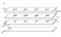
積層発光体(1)は、水平板形状の電子回路基板(11)と、前記電子回路基板の表面側(図1で示す上面側)に半田付けで固着実装した複数のLED(12)と、前記電子回路基板へ電気を供給する接続コネクタ(13)と、前記電子回路基板の表面側に積層して設ける第一炭素繊維強化プラスチック体(31)と、前記電子回路基板の裏面側(図1で示す下面側)に積層して設ける第二炭素繊維強化プラスチック体(32)と、前記電子回路基板と前記第一炭素繊維強化プラスチック体との間に挟設する絶縁層(20)と、で構成する(図1)。 The laminated light emitter (1) includes a horizontal plate-shaped electronic circuit board (11), and a plurality of LEDs (12) fixedly mounted by soldering on the surface side (the upper surface side shown in FIG. 1) of the electronic circuit board, A connector (13) for supplying electricity to the electronic circuit board, a first carbon fiber reinforced plastic body (31) provided by being laminated on the front surface side of the electronic circuit board, and a back surface side of the electronic circuit board (FIG. 1). A second carbon fiber reinforced plastic body (32) provided by being laminated on the lower surface side, and an insulating layer (20) sandwiched between the electronic circuit board and the first carbon fiber reinforced plastic body. Configure (FIG. 1).
前記LED(12)に替えて、その他の発光する部品を固着実装してもよいものとする。 Instead of the LED (12), other light emitting components may be fixedly mounted.
前記LED(12)実装後の先端部状態について、接触による損傷防止の観点からは図2のように前記第一炭素繊維強化プラスチック体(31)の表面から突出しない方が好ましいが、LEDから放射される光の遮光の観点からは図3のように前記第一炭素繊維強化プラスチック体(31)の表面から突出する方が好ましい(図2及び図3)。 From the viewpoint of preventing damage due to contact, it is preferable that the state of the tip after mounting the LED (12) does not protrude from the surface of the first carbon fiber reinforced plastic body (31) as shown in FIG. From the viewpoint of shielding light, it is preferable to project from the surface of the first carbon fiber reinforced plastic body (31) as shown in FIG. 3 (FIGS. 2 and 3).
前記絶縁層(20)について、前記電子回路基板(11)のうち前記LED(12)実装側の面と前記第一炭素繊維強化プラスチック体(31)又は前記第二炭素繊維強化プラスチック体(32)との間あるいは前記電子回路基板のうちLED非実装側の面と前記第一炭素繊維強化プラスチック体又は前記第二炭素繊維強化プラスチック体との間に挟設され、電気等の伝導を絶つ機能を有する層の総称を示すものとし、少なくとも、電子回路基板のLED実装側(電子部品半田付け側)の面と第一炭素繊維強化プラスチック体との間に挟設する必要がある(図1)。 About the said insulating layer (20), the said LED (12) mounting side surface and said 1st carbon fiber reinforced plastic body (31) or said 2nd carbon fiber reinforced plastic body (32) among the said electronic circuit boards (11). Or between the surface of the electronic circuit board on the LED non-mounting side and the first carbon fiber reinforced plastic body or the second carbon fiber reinforced plastic body, and has a function of cutting off the conduction of electricity, etc. It is necessary to indicate a generic name of the layers to be included, and at least between the LED mounting side (electronic component soldering side) surface of the electronic circuit board and the first carbon fiber reinforced plastic body (FIG. 1).
本実施例においては、図1で示すように前記電子回路基板(11)のうち前記LED(12)実装側である表面側に設ける第一絶縁体(21)のみで構成するが、前記LED非実装側である裏面側に第二絶縁体を挟設しても良い。仮に、第二絶縁体を挟設した場合、積層成形体全体としての構造バランスがよくなる、接着時の加圧工程の調整が容易となる等の効果も生じ得る。 In this embodiment, as shown in FIG. 1, the electronic circuit board (11) is composed of only the first insulator (21) provided on the surface side which is the LED (12) mounting side. A second insulator may be sandwiched on the back side that is the mounting side. If the second insulator is sandwiched, effects such as improved structural balance as a whole laminated molded body and easy adjustment of the pressurizing process during bonding may occur.
前記絶縁層(20)を構成する前記第一絶縁体(21)の孔部の大きさ及び形状について、当該LED(12)の固着実装を行うため及び当該LEDによる放射光の遮光防止のため、当該LEDに対応する部分に、当該LEDが通過する程度の大きさの矩形の孔部を設けている(図1)。 For the size and shape of the hole of the first insulator (21) constituting the insulating layer (20), in order to fix and mount the LED (12) and to prevent the emitted light from being blocked by the LED, A rectangular hole having a size that allows the LED to pass therethrough is provided in a portion corresponding to the LED (FIG. 1).
また、前記第一絶縁体(21)の場合と同様に、前記第一炭素繊維強化プラスチック体(31)の当該LED(12)に対応する部分にも、当該LEDが通過する程度の大きさの矩形の孔部を設けている(図1)。 Similarly to the case of the first insulator (21), the portion of the first carbon fiber reinforced plastic body (31) corresponding to the LED (12) is large enough to pass the LED. A rectangular hole is provided (FIG. 1).
前記第一炭素繊維強化プラスチック体(31)の大きさについて、積層成形体としての強度が確保されていれば前記電子回路基板(11)の表面側よりも小さくても許容し得るが、好ましくは前記電子回路基板の表面側及び前記第一絶縁体(21)の表面側全体を覆う大きさである(図1)。 Regarding the size of the first carbon fiber reinforced plastic body (31), if the strength as a laminated molded body is ensured, it is acceptable even if it is smaller than the surface side of the electronic circuit board (11), preferably The size covers the entire surface side of the electronic circuit board and the surface side of the first insulator (21) (FIG. 1).
前記第二炭素繊維強化プラスチック体(32)の厚み、形状及び大きさについて、前記第一炭素繊維強化プラスチック体(31)と同様、積層成形体としての強度が確保されていればいかなる厚み、形状及び大きさでも許容し得るが、接着時の加圧工程の調整が容易性、積層成形体全体としての構造バランスを考慮すると、前記第一炭素繊維強化プラスチック体と厚みが同一である方が好ましい。また、前記第一炭素繊維強化プラスチック体と形状及び大きさも同一であればさらに好ましい(図1)。 Regarding the thickness, shape and size of the second carbon fiber reinforced plastic body (32), as with the first carbon fiber reinforced plastic body (31), any thickness and shape can be used as long as the strength as a laminated molded body is secured. However, it is preferable that the thickness is the same as that of the first carbon fiber reinforced plastic body in consideration of the ease of adjustment of the pressurizing process at the time of bonding and the structural balance of the entire laminated molded body. . Further, it is more preferable if the shape and size are the same as those of the first carbon fiber reinforced plastic body (FIG. 1).
次に、積層発光体から光が放射される作動について、図1に従い、説明する。 Next, the operation of emitting light from the laminated illuminant will be described with reference to FIG.
接続コネクタ(13)を介して電気の供給を受け、電子回路基板(11)に固着実装したLED(12)が発光することにより、当該積層発光体(1)から光が放射される。 Light is emitted from the laminated light emitting body (1) when the LED (12) fixedly mounted on the electronic circuit board (11) emits light by being supplied with electricity through the connection connector (13).
次に、積層発光体の製造方法について、図1に従い、説明する。 Next, the manufacturing method of a laminated light-emitting body is demonstrated according to FIG.
電子回路基板(11)の表面側に絶縁層(20)を載置する。 An insulating layer (20) is placed on the surface side of the electronic circuit board (11).
前記絶縁層(20)の上部方向から第一炭素繊維強化プラスチック体(31)で、前記電子回路基板(11)の下部方向から第二炭素繊維強化プラスチック体(32)で両側から挟み、加圧及び加熱しながら接着し一体的に成形する。 The first carbon fiber reinforced plastic body (31) from the upper direction of the insulating layer (20) and the second carbon fiber reinforced plastic body (32) from the lower direction of the electronic circuit board (11) are sandwiched from both sides and pressed. Then, it is bonded and integrally molded while heating.
実施例2は、電子回路基板が電子回路基板の厚さ方向に変位する断面台形形状である積層発光体であり、例えば、車両のヘッドライトとしての利用を想定(提案)する。その構成について、実施例1と異なる部分について図4に従い、説明する。 Example 2 is a laminated light-emitting body having a trapezoidal cross section in which an electronic circuit board is displaced in the thickness direction of the electronic circuit board. For example, it is assumed (suggested) to be used as a vehicle headlight. The configuration will be described with reference to FIG.
積層発光体(1)は、断面台形形状の電子回路基板(11)と、前記電子回路基板の表面側に半田付けで固着実装した複数のLED(12)と、前記電子回路基板へ電気を供給する接続コネクタ(図示せず)と、前記電子回路基板の表面側に積層して設ける第一炭素繊維強化プラスチック体(31)と、前記電子回路基板の裏面側に積層して設ける第二炭素繊維強化プラスチック体(32)と、前記電子回路基板と前記第一炭素繊維強化プラスチック体との間及び前記電子回路基板と前記第二炭素繊維強化プラスチック体との間に挟設する絶縁層(20)と、で構成する。 The multilayer light emitter (1) supplies electricity to the electronic circuit board (11) having a trapezoidal cross section, a plurality of LEDs (12) fixedly mounted by soldering on the surface side of the electronic circuit board, and the electronic circuit board. Connecting connector (not shown), a first carbon fiber reinforced plastic body (31) provided by being laminated on the front side of the electronic circuit board, and a second carbon fiber provided by being laminated on the back side of the electronic circuit board An insulating layer (20) sandwiched between a reinforced plastic body (32) and the electronic circuit board and the first carbon fiber reinforced plastic body and between the electronic circuit board and the second carbon fiber reinforced plastic body. And consist of:
前記電子回路基板(11)について断面台形形状とは、実施例1のような水平板形状の電子回路基板に比べ、電子回路基板の厚さ方向に形状が変位する形状を指すものとし、その断面が台形形状となるものをいう。 The trapezoidal shape of the cross section of the electronic circuit board (11) refers to a shape whose shape is displaced in the thickness direction of the electronic circuit board as compared to the horizontal board-shaped electronic circuit board as in the first embodiment. Means a trapezoidal shape.
前記絶縁層(20)は、前記電子回路基板(11)と前記第一炭素繊維強化プラスチック体(31)との間に挟設する第一絶縁体(21)と、前記電子回路基板と前記第二炭素繊維強化プラスチック体(32)との間に挟設する第二絶縁体(22)と、で構成する。 The insulating layer (20) includes a first insulator (21) sandwiched between the electronic circuit board (11) and the first carbon fiber reinforced plastic body (31), the electronic circuit board, and the first And a second insulator (22) sandwiched between the two-carbon fiber reinforced plastic body (32).
その他の構成については、実施例1と同様であるため、省略する。また、積層発光体から光が放射される作動については、実施例1と同様であるため、省略する。 Other configurations are the same as those in the first embodiment, and are omitted. The operation of emitting light from the laminated illuminator is the same as that of the first embodiment, and is therefore omitted.
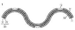
実施例3は、電子回路基板が電子回路基板の厚さ方向に変位する断面波形状である積層発光体であり、例えば、照明設備としての利用を想定(提案)する。その構成について、実施例2と異なる部分について図5に従い説明する。 Example 3 is a laminated light-emitting body having a cross-sectional wave shape in which an electronic circuit board is displaced in the thickness direction of the electronic circuit board. For example, it is assumed (suggested) for use as lighting equipment. With respect to the configuration, portions different from the second embodiment will be described with reference to FIG.
積層発光体(1)は、断面波形状の電子回路基板(11)と、前記電子回路基板の表面側及び裏面側に半田付けで固着実装した複数のLED(12)と、前記電子回路基板へ電気を供給する接続コネクタ(図示せず)と、前記電子回路基板の表面側に積層して設ける第一炭素繊維強化プラスチック体(31)と、前記電子回路基板の裏面側に積層して設ける第二炭素繊維強化プラスチック体(32)と、前記電子回路基板と前記第一炭素繊維強化プラスチック体との間及び前記電子回路基板と前記第二炭素繊維強化プラスチック体との間に挟設する絶縁層(20)と、で構成する。 The multilayer illuminator (1) includes an electronic circuit board (11) having a cross-sectional wave shape, a plurality of LEDs (12) fixedly mounted by soldering on the front and back sides of the electronic circuit board, and the electronic circuit board. A connector (not shown) for supplying electricity, a first carbon fiber reinforced plastic body (31) provided by being laminated on the surface side of the electronic circuit board, and a first layer provided by being laminated on the back side of the electronic circuit board An insulating layer sandwiched between a two-carbon fiber reinforced plastic body (32), the electronic circuit board and the first carbon fiber reinforced plastic body, and between the electronic circuit board and the second carbon fiber reinforced plastic body. (20).
前記電子回路基板(11)について断面波形形状とは、実施例1のような水平板形状の電子回路基板に比べ、電子回路基板の厚さ方向に形状が変位する形状を指すものとし、その断面が波形形状となるものをいう。 The cross-sectional corrugated shape of the electronic circuit board (11) refers to a shape whose shape is displaced in the thickness direction of the electronic circuit board as compared to the horizontal-plate-shaped electronic circuit board as in the first embodiment. Is a waveform.
前記絶縁層(20)は、前記電子回路基板(11)と前記第一炭素繊維強化プラスチック体(31)との間に挟設する第一絶縁体(21)と、前記電子回路基板と前記第二炭素繊維強化プラスチック体(32)との間に挟設する第二絶縁体(22)と、で構成する。 The insulating layer (20) includes a first insulator (21) sandwiched between the electronic circuit board (11) and the first carbon fiber reinforced plastic body (31), the electronic circuit board, and the first And a second insulator (22) sandwiched between the two-carbon fiber reinforced plastic body (32).
その他の構成については、実施例2と同様であるため、省略する。 Other configurations are the same as those in the second embodiment, and thus are omitted.
次に、積層発光体から光が放射される作動について、図5に従い、説明する。 Next, the operation of emitting light from the laminated illuminant will be described with reference to FIG.
図示しない接続コネクタを介して電気の供給を受け、電子回路基板(11)の表面側及び裏面側に固着実装したLED(12)が発光することにより、当該積層発光体(1)から光が放射される。 Light is emitted from the laminated light emitter (1) by receiving electricity from a connection connector (not shown) and emitting light from the LED (12) fixedly mounted on the front side and the back side of the electronic circuit board (11). Is done.
本願発明の積層成形体及び積層発光体は、電子回路基板を内蔵しながら構造物との一体化を図ることで、組立工程が介在せず、既存の組立品を置き換えられる積層成形体及び積層発光体であるので、産業上の利用可能性を有する。 The laminated molded body and the laminated light emitting body of the present invention can be integrated with a structure while incorporating an electronic circuit board, so that an existing assembly can be replaced without an assembly process and a laminated light emitting body. Because it is a body, it has industrial applicability.
1 積層発光体(積層成形体)
11 電子回路基板
12 LED(発光する部品)
13 接続コネクタ(電気供給部)
20 絶縁層
21 第一絶縁体
22 第二絶縁体
31 第一炭素繊維強化プラスチック体
32 第二炭素繊維強化プラスチック体1 Laminated light emitter (laminated molded body)
11
13 Connector (Electric power supply)
20 Insulating
Claims (5)
Translated fromJapanese前記電子回路基板の表面側に積層して設ける第一炭素繊維強化プラスチック体(31)と、
前記電子回路基板の裏面側に積層して設ける第二炭素繊維強化プラスチック体(32)と、
前記電子回路基板のうち前記所定の部品を固着実装した側の面と前記第一炭素繊維強化プラスチック体又は前記第二炭素繊維強化プラスチック体との間に挟設する絶縁層(20)と、
からなり、
前記電子回路基板、前記絶縁層、前記第一炭素繊維強化プラスチック体及び前記第二炭素繊維強化プラスチック体を接着により一体化した積層成形体。A predetermined-shaped electronic circuit board (11) in which a predetermined component is fixedly mounted on at least one of the front surface side or the back surface side;
A first carbon fiber reinforced plastic body (31) provided on the surface side of the electronic circuit board;
A second carbon fiber reinforced plastic body (32) provided by being laminated on the back side of the electronic circuit board;
An insulating layer (20) sandwiched between a surface of the electronic circuit board on which the predetermined component is fixedly mounted and the first carbon fiber reinforced plastic body or the second carbon fiber reinforced plastic body;
Consists of
A laminated molded body in which the electronic circuit board, the insulating layer, the first carbon fiber reinforced plastic body, and the second carbon fiber reinforced plastic body are integrated by bonding.
Applications Claiming Priority (1)
| Application Number | Priority Date | Filing Date | Title |
|---|---|---|---|
| PCT/JP2015/053045WO2016125261A1 (en) | 2015-02-04 | 2015-02-04 | Laminated molded body and laminated light-emitting body |
Publications (2)
| Publication Number | Publication Date |
|---|---|
| JPWO2016125261A1true JPWO2016125261A1 (en) | 2017-10-19 |
| JP6454737B2 JP6454737B2 (en) | 2019-01-16 |
Family
ID=56563626
Family Applications (1)
| Application Number | Title | Priority Date | Filing Date |
|---|---|---|---|
| JP2016572987AExpired - Fee RelatedJP6454737B2 (en) | 2015-02-04 | 2015-02-04 | Laminated molded body and laminated light emitting body |
Country Status (2)
| Country | Link |
|---|---|
| JP (1) | JP6454737B2 (en) |
| WO (1) | WO2016125261A1 (en) |
Families Citing this family (2)
| Publication number | Priority date | Publication date | Assignee | Title |
|---|---|---|---|---|
| WO2021217418A1 (en)* | 2020-04-28 | 2021-11-04 | 南昌欧菲显示科技有限公司 | Light-emitting module and ar glasses |
| US12385619B1 (en) | 2024-05-13 | 2025-08-12 | GM Global Technology Operations LLC | Lighting device for a vehicle |
Citations (6)
| Publication number | Priority date | Publication date | Assignee | Title |
|---|---|---|---|---|
| JP2005129734A (en)* | 2003-10-23 | 2005-05-19 | Sony Corp | Electronic device |
| JP2011249535A (en)* | 2010-05-26 | 2011-12-08 | Daisho Denshi Co Ltd | Flexible wiring board, light-emitting module, manufacturing method of light-emitting module and manufacturing method of flexible wiring board |
| US20120120651A1 (en)* | 2010-11-16 | 2012-05-17 | John Patrick Peck | Led luminaire utilizing an extended and non-metallic enclosure |
| JP2012160430A (en)* | 2011-01-14 | 2012-08-23 | Koito Mfg Co Ltd | Lighting system |
| WO2013021987A1 (en)* | 2011-08-10 | 2013-02-14 | 日本電気株式会社 | Light guiding module and electronic device equipped with same |
| JP2015008163A (en)* | 2014-10-15 | 2015-01-15 | 岩崎電気株式会社 | LED lamp |
- 2015
- 2015-02-04WOPCT/JP2015/053045patent/WO2016125261A1/ennot_activeCeased
- 2015-02-04JPJP2016572987Apatent/JP6454737B2/ennot_activeExpired - Fee Related
Patent Citations (6)
| Publication number | Priority date | Publication date | Assignee | Title |
|---|---|---|---|---|
| JP2005129734A (en)* | 2003-10-23 | 2005-05-19 | Sony Corp | Electronic device |
| JP2011249535A (en)* | 2010-05-26 | 2011-12-08 | Daisho Denshi Co Ltd | Flexible wiring board, light-emitting module, manufacturing method of light-emitting module and manufacturing method of flexible wiring board |
| US20120120651A1 (en)* | 2010-11-16 | 2012-05-17 | John Patrick Peck | Led luminaire utilizing an extended and non-metallic enclosure |
| JP2012160430A (en)* | 2011-01-14 | 2012-08-23 | Koito Mfg Co Ltd | Lighting system |
| WO2013021987A1 (en)* | 2011-08-10 | 2013-02-14 | 日本電気株式会社 | Light guiding module and electronic device equipped with same |
| JP2015008163A (en)* | 2014-10-15 | 2015-01-15 | 岩崎電気株式会社 | LED lamp |
Also Published As
| Publication number | Publication date |
|---|---|
| WO2016125261A1 (en) | 2016-08-11 |
| JP6454737B2 (en) | 2019-01-16 |
Similar Documents
| Publication | Publication Date | Title |
|---|---|---|
| CN107112735B (en) | The manufacturing method of electric circuit structure, connection box and electric circuit structure | |
| CN110431664B (en) | Mounting LED elements on a flat carrier | |
| JP6945187B2 (en) | Manufacturing method of power supply, lighting equipment, mobile body and power supply | |
| KR101398701B1 (en) | Led device, manufacturing method thereof, and light-emitting device | |
| US20110299292A1 (en) | Flexirigid support plate | |
| JP2012253213A (en) | Connection structure of wiring bodies, wiring body, electronic apparatus, and manufacturing method of electronic apparatus | |
| WO2009067556A3 (en) | Apparatus and methods for thermal management of light emitting diodes | |
| JP6477373B2 (en) | Circuit assembly and electrical junction box | |
| US20180375307A1 (en) | Electrical junction box | |
| JP6454737B2 (en) | Laminated molded body and laminated light emitting body | |
| WO2012026058A1 (en) | Light-emitting device | |
| KR20120097802A (en) | Flexible Board Structure | |
| CN105493279B (en) | System for attaching devices to flexible substrates | |
| JP2013247168A (en) | Power supply device | |
| JP2016225255A (en) | Illumination fixture | |
| JP6089713B2 (en) | Electronics | |
| KR200473652Y1 (en) | Led cooling structure | |
| JP6458696B2 (en) | Printed wiring board connection structure and light emitting module having the connection structure | |
| JP2017055077A (en) | Electric equipment and power converter | |
| WO2021117489A1 (en) | Lamp unit and vehicle lamp provided therewith | |
| JP2017037707A (en) | Lighting fixture optical semiconductor unit and lighting fixture optical semiconductor unit manufacturing method | |
| JP2012119509A (en) | Circuit module and lighting device equipped with the circuit module | |
| WO2016104609A1 (en) | Led element substrate, led-mounted module and led display device using these | |
| ITUB20155335A1 (en) | MOUNTING STRUCTURE FOR LIGHTING DEVICES, LIGHTING DEVICE AND CORRESPONDENT PROCEDURE | |
| JP2008016657A (en) | Structure of electronic equipment |
Legal Events
| Date | Code | Title | Description |
|---|---|---|---|
| A621 | Written request for application examination | Free format text:JAPANESE INTERMEDIATE CODE: A621 Effective date:20170710 | |
| A131 | Notification of reasons for refusal | Free format text:JAPANESE INTERMEDIATE CODE: A131 Effective date:20180710 | |
| A521 | Request for written amendment filed | Free format text:JAPANESE INTERMEDIATE CODE: A523 Effective date:20180831 | |
| TRDD | Decision of grant or rejection written | ||
| A01 | Written decision to grant a patent or to grant a registration (utility model) | Free format text:JAPANESE INTERMEDIATE CODE: A01 Effective date:20181211 | |
| A61 | First payment of annual fees (during grant procedure) | Free format text:JAPANESE INTERMEDIATE CODE: A61 Effective date:20181217 | |
| R150 | Certificate of patent or registration of utility model | Ref document number:6454737 Country of ref document:JP Free format text:JAPANESE INTERMEDIATE CODE: R150 | |
| S531 | Written request for registration of change of domicile | Free format text:JAPANESE INTERMEDIATE CODE: R313531 | |
| R350 | Written notification of registration of transfer | Free format text:JAPANESE INTERMEDIATE CODE: R350 | |
| R250 | Receipt of annual fees | Free format text:JAPANESE INTERMEDIATE CODE: R250 | |
| LAPS | Cancellation because of no payment of annual fees |