JPWO2016084256A1 - Light emitting device - Google Patents
Light emitting deviceDownload PDFInfo
- Publication number
- JPWO2016084256A1 JPWO2016084256A1JP2016561204AJP2016561204AJPWO2016084256A1JP WO2016084256 A1JPWO2016084256 A1JP WO2016084256A1JP 2016561204 AJP2016561204 AJP 2016561204AJP 2016561204 AJP2016561204 AJP 2016561204AJP WO2016084256 A1JPWO2016084256 A1JP WO2016084256A1
- Authority
- JP
- Japan
- Prior art keywords
- layer
- terminal
- light emitting
- electrode
- emitting device
- Prior art date
- Legal status (The legal status is an assumption and is not a legal conclusion. Google has not performed a legal analysis and makes no representation as to the accuracy of the status listed.)
- Granted
Links
Images


Classifications
- H—ELECTRICITY
- H05—ELECTRIC TECHNIQUES NOT OTHERWISE PROVIDED FOR
- H05B—ELECTRIC HEATING; ELECTRIC LIGHT SOURCES NOT OTHERWISE PROVIDED FOR; CIRCUIT ARRANGEMENTS FOR ELECTRIC LIGHT SOURCES, IN GENERAL
- H05B33/00—Electroluminescent light sources
- H05B33/02—Details
- H05B33/04—Sealing arrangements, e.g. against humidity
- H—ELECTRICITY
- H10—SEMICONDUCTOR DEVICES; ELECTRIC SOLID-STATE DEVICES NOT OTHERWISE PROVIDED FOR
- H10K—ORGANIC ELECTRIC SOLID-STATE DEVICES
- H10K50/00—Organic light-emitting devices
- H10K50/80—Constructional details
- H10K50/805—Electrodes
- H—ELECTRICITY
- H10—SEMICONDUCTOR DEVICES; ELECTRIC SOLID-STATE DEVICES NOT OTHERWISE PROVIDED FOR
- H10K—ORGANIC ELECTRIC SOLID-STATE DEVICES
- H10K50/00—Organic light-emitting devices
- H10K50/80—Constructional details
- H10K50/84—Passivation; Containers; Encapsulations
- H10K50/841—Self-supporting sealing arrangements
- H—ELECTRICITY
- H10—SEMICONDUCTOR DEVICES; ELECTRIC SOLID-STATE DEVICES NOT OTHERWISE PROVIDED FOR
- H10K—ORGANIC ELECTRIC SOLID-STATE DEVICES
- H10K50/00—Organic light-emitting devices
- H10K50/80—Constructional details
- H10K50/84—Passivation; Containers; Encapsulations
- H10K50/842—Containers
- H10K50/8426—Peripheral sealing arrangements, e.g. adhesives, sealants
- H—ELECTRICITY
- H10—SEMICONDUCTOR DEVICES; ELECTRIC SOLID-STATE DEVICES NOT OTHERWISE PROVIDED FOR
- H10K—ORGANIC ELECTRIC SOLID-STATE DEVICES
- H10K50/00—Organic light-emitting devices
- H10K50/80—Constructional details
- H10K50/88—Terminals, e.g. bond pads
- H—ELECTRICITY
- H10—SEMICONDUCTOR DEVICES; ELECTRIC SOLID-STATE DEVICES NOT OTHERWISE PROVIDED FOR
- H10K—ORGANIC ELECTRIC SOLID-STATE DEVICES
- H10K77/00—Constructional details of devices covered by this subclass and not covered by groups H10K10/80, H10K30/80, H10K50/80 or H10K59/80
- H10K77/10—Substrates, e.g. flexible substrates
- H10K77/111—Flexible substrates
- H—ELECTRICITY
- H10—SEMICONDUCTOR DEVICES; ELECTRIC SOLID-STATE DEVICES NOT OTHERWISE PROVIDED FOR
- H10K—ORGANIC ELECTRIC SOLID-STATE DEVICES
- H10K71/00—Manufacture or treatment specially adapted for the organic devices covered by this subclass
- H10K71/20—Changing the shape of the active layer in the devices, e.g. patterning
- H10K71/221—Changing the shape of the active layer in the devices, e.g. patterning by lift-off techniques
- Y—GENERAL TAGGING OF NEW TECHNOLOGICAL DEVELOPMENTS; GENERAL TAGGING OF CROSS-SECTIONAL TECHNOLOGIES SPANNING OVER SEVERAL SECTIONS OF THE IPC; TECHNICAL SUBJECTS COVERED BY FORMER USPC CROSS-REFERENCE ART COLLECTIONS [XRACs] AND DIGESTS
- Y02—TECHNOLOGIES OR APPLICATIONS FOR MITIGATION OR ADAPTATION AGAINST CLIMATE CHANGE
- Y02E—REDUCTION OF GREENHOUSE GAS [GHG] EMISSIONS, RELATED TO ENERGY GENERATION, TRANSMISSION OR DISTRIBUTION
- Y02E10/00—Energy generation through renewable energy sources
- Y02E10/50—Photovoltaic [PV] energy
- Y02E10/549—Organic PV cells
Landscapes
- Physics & Mathematics (AREA)
- Optics & Photonics (AREA)
- Electroluminescent Light Sources (AREA)
Abstract
Translated fromJapaneseDescription
Translated fromJapanese本発明は、発光装置に関する。 The present invention relates to a light emitting device.
近年は、発光部に有機EL(Organic Electroluminescence)素子を有する発光装置の開発が進んでいる。有機EL素子は、有機層を、第1電極及び第2電極で挟んだ構成を有している。有機層は水分や酸素に弱いため、発光部は封止される必要がある。発光部を封止する方法の一つに、封止層を用いる方法がある。封止層を形成する方法としては、ALD(Atomic Layer Deposition)法、CVD法、又はスパッタリング法などの気相成膜法がある。 In recent years, a light emitting device having an organic EL (Organic Electroluminescence) element in a light emitting portion has been developed. The organic EL element has a configuration in which an organic layer is sandwiched between a first electrode and a second electrode. Since the organic layer is vulnerable to moisture and oxygen, the light emitting portion needs to be sealed. One method for sealing the light emitting part is to use a sealing layer. As a method for forming the sealing layer, there is a vapor deposition method such as an ALD (Atomic Layer Deposition) method, a CVD method, or a sputtering method.
なお、特許文献1には、磁気記録媒体において、磁気記録層の上に凸パターンを形成する際に、リフトオフ法を用いることが記載されている。 Japanese Patent Application Laid-Open No. H10-228561 describes that a lift-off method is used when a convex pattern is formed on a magnetic recording layer in a magnetic recording medium.
発光装置の基板には、上記した発光部の他に、発光部に接続する端子も形成されている。一方、封止層は一般的に気相法で形成されているため、端子の上にも形成されてしまう。このため、封止層を端子の上から除去する必要がある。 In addition to the light emitting portion described above, a terminal connected to the light emitting portion is also formed on the substrate of the light emitting device. On the other hand, since the sealing layer is generally formed by a vapor phase method, it is also formed on the terminal. For this reason, it is necessary to remove the sealing layer from above the terminals.
本発明が解決しようとする課題としては、封止層を端子の上から容易に除去できるようにすることが一例として挙げられる。 An example of a problem to be solved by the present invention is that the sealing layer can be easily removed from above the terminal.
請求項1に記載の発明は、基板と、
前記基板に形成された発光部と、
前記基板に形成され、前記発光部に電気的に接続する端子と、
前記基板に形成され、前記発光部を封止し、かつ前記端子を覆っていない封止層と、
前記封止層の上に形成され、前記封止層とは異なる材料によって形成されている被覆層と、
を備え、
前記端子の隣に位置する領域の少なくとも一部において、前記被覆層の端部は前記封止層の端部より外側にある発光装置である。The invention according to
A light emitting part formed on the substrate;
A terminal formed on the substrate and electrically connected to the light emitting unit;
A sealing layer that is formed on the substrate, seals the light emitting portion, and does not cover the terminals;
A coating layer formed on the sealing layer and formed of a material different from the sealing layer;
With
In at least a part of a region located next to the terminal, the end portion of the covering layer is a light emitting device located outside the end portion of the sealing layer.
上述した目的、およびその他の目的、特徴および利点は、以下に述べる好適な実施の形態、およびそれに付随する以下の図面によってさらに明らかになる。 The above-described object and other objects, features, and advantages will become more apparent from the preferred embodiments described below and the accompanying drawings.
以下、本発明の実施の形態について、図面を用いて説明する。尚、すべての図面において、同様な構成要素には同様の符号を付し、適宜説明を省略する。 Hereinafter, embodiments of the present invention will be described with reference to the drawings. In all the drawings, the same reference numerals are given to the same components, and the description will be omitted as appropriate.
(第1の実施形態)
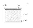
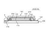
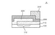
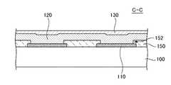
図1は、第1の実施形態に係る発光装置10の構成を示す平面図である。図2は、図1から被覆層210、封止層200、及び第2電極130を取り除いた図である。図3は図2から絶縁層150及び有機層120を取り除いた図である。図4は、図1のA−A断面図である。図5は、図4の点線αで囲んだ領域を拡大した図である。(First embodiment)
FIG. 1 is a plan view showing a configuration of a
実施形態に係る発光装置10は、図1及び図4に示すように、基板100、発光部140、第1端子112、第2端子132、封止層200、及び被覆層210を備えている。発光部140は基板100の第1面102に形成されている。第1端子112及び第2端子132は基板100の第1面102に形成されており、発光部140に電気的に接続している。封止層200は基板100の第1面102に形成されており、発光部140を封止している。また、封止層200は第1端子112及び第2端子132を覆っていない。被覆層210は封止層200の上に形成されており、被覆層210とは異なる材料によって形成されている。そして、図1、図4、及び図5に示すように、第1端子112の隣に位置する領域及び第2端子132の隣に位置する領域の少なくとも一部において、被覆層210の端部の一部は封止層200から食み出しており、突出部212となっている。言い換えると、被覆層210の端部の少なくとも一部は封止層200の端部より外側にある。発光装置10は、照明装置又はディスプレイであるが、図1〜図4は、発光装置10が照明装置の場合を示している。以下、詳細に説明する。 As shown in FIGS. 1 and 4, the
まず、図1〜図4を用いて発光装置10について説明する。 First, the
発光装置10がボトムエミッション型の発光装置である場合、基板100は、例えばガラス基板や樹脂基板などの透光性を有する基板である。一方、発光装置10がトップエミッション型の発光装置である場合、基板100は透光性を有していなくてもよい。また、基板100は可撓性を有していてもよい。可撓性を有している場合、基板100の厚さは、例えば10μm以上1000μm以下である。基板100は、例えば矩形などの多角形である。基板100が樹脂基板である場合、基板100は、例えばPEN(ポリエチレンナフタレート)、PES(ポリエーテルサルホン)、PET(ポリエチレンテレフタラート)、又はポリイミドを用いて形成されている。また、基板100が樹脂基板である場合、水分が基板100を透過することを抑制するために、基板100の少なくとも一面(好ましくは両面)に、SiNxやSiONなどの無機バリア膜が形成されている。なお、この無機バリア膜と基板100の間に、平坦化層(例えば有機層)が設けられていてもよい。When the
基板100の第1面102には、発光部140が形成されている。発光部140は、第1電極110、有機層120、及び第2電極130をこの順に積層させた構成を有している。 A
第1電極110は、光透過性を有する透明電極である。透明電極の材料は、金属を含む材料、例えば、ITO(Indium Tin Oxide)、IZO(Indium Zinc Oxide)、IWZO(Indium Tungsten Zinc Oxide)、ZnO(Zinc Oxide)等の金属酸化物である。第1電極110の厚さは、例えば10nm以上500nm以下である。第1電極110は、例えばスパッタリング法又は蒸着法を用いて形成される。なお、第1電極110は、カーボンナノチューブ、PEDOT/PSSなどの導電性有機材料を用いて形成されていてもよい。 The
有機層120は発光層を有している。有機層120は、例えば、正孔注入層、発光層、及び電子注入層をこの順に積層させた構成を有している。正孔注入層と発光層との間には正孔輸送層が形成されていてもよい。また、発光層と電子注入層との間には電子輸送層が形成されていてもよい。有機層120は蒸着法で形成されてもよい。また、有機層120のうち少なくとも一つの層、例えば第1電極110と接触する層は、インクジェット法、印刷法、又はスプレー法などの塗布法によって形成されてもよい。なお、この場合、有機層120の残りの層は、蒸着法によって形成されている。また、有機層120のすべての層が、塗布法を用いて形成されていてもよい。 The
第2電極130は、例えば、Al、Au、Ag(AgインクやAgナノワイヤの場合もある)、Pt、Mg、Sn、Zn、及びInからなる第1群の中から選択される金属、又はこの第1群から選択される金属の合金からなる金属層を含んでいる。この場合、第2電極130は遮光性を有している。第2電極130の厚さは、例えば10nm以上500nm以下である。ただし、第2電極130は、第1電極110の材料として例示した材料を用いて形成されていてもよい。第2電極130は、例えばスパッタリング法又は蒸着法を用いて形成される。 The
なお、上記した第1電極110及び第2電極130の材料は、発光装置10がボトムエミッション型の場合である。発光装置10がトップエミッション型の場合、第1電極110の材料と第2電極130の材料は逆になる。すなわち第1電極110の材料には上記した第2電極130の材料が用いられ、第2電極130の材料には上記した第1電極110の材料が用いられる。 Note that the materials of the
第1電極110の縁は、絶縁層150によって覆われている。絶縁層150は例えばポリイミドなどの感光性の樹脂材料によって形成されており、第1電極110のうち発光部140の発光領域となる部分を囲んでいる。絶縁層150を設けることにより、第1電極110の縁において第1電極110と第2電極130が短絡することを抑制できる。 The edge of the
また、発光装置10は、第1端子112及び第2端子132を有している。第1端子112は第1電極110に接続しており、第2端子132は第2電極130に接続している。第1端子112及び第2端子132は、例えば、第1電極110と同一の材料で形成された層を有している。なお、第1端子112と第1電極110の間には引出配線が設けられていてもよい。また、第2端子132と第2電極130の間にも引出配線が設けられていてもよい。 In addition, the
第1端子112には、ボンディングワイヤ、又はリード端子などの導電部材(電子部品の一例)を介して制御回路の正極端子が接続され、第2端子132には、ボンディングワイヤ又はリード端子などの導電部材を介して制御回路の負極端子が接続される。ただし第1端子112及び第2端子132の少なくとも一方には、半導体パッケージなどの回路素子が直接接続されてもよい。また第1端子112及び第2端子132は、フレキシブルプリント基板(FPC)を介して制御回路に接続されていてもよい。この場合、第1端子112及び第2端子132は、例えば異方性導電性樹脂を介してFPCと接続する。 The
基板100には、さらに封止層200及び被覆層210が設けられている。 The
封止層200は、基板100のうち発光部140が形成されている面に形成されており、発光部140を覆っている。ただし、第1端子112及び第2端子132は封止層200で覆われていない。封止層200は、例えば絶縁材料、さらに具体的には無機材料によって形成されている。また、封止層200の厚さは、好ましくは300nm以下である。また封止層200の厚さは、例えば50nm以上である。封止層200は、ALD(Atomic Layer Deposition)法を用いて形成されている。ALD法を用いることにより、封止層200の段差被覆性は高くなる。ただし封止層200は、他の成膜法、例えばCVD法やスパッタリング法を用いて形成されていてもよい。 The
封止層200は、複数の層を積層した多層構造を有していてもよい。この場合、第1の材料からなる第1封止層と、第2の材料からなる第2封止層とを繰り返し積層した構造を有していてもよい。最下層は第1封止層及び第2封止層のいずれであってもよい。また、最上層も第1封止層及び第2封止層のいずれであってもよい。また、封止膜200は第1の材料と第2の材料の混在する単層であってもよい。 The
被覆層210は、封止層200を保護している。具体的には、被覆層210は、少なくとも発光部140と重なる領域に形成されているが、第1端子112の大部分及び第2端子132の大部分とは重なっていない。被覆層210は、エポキシ樹脂などの熱硬化型の樹脂を用いて形成されている。ただし被覆層210は、光硬化型の樹脂であってもよいし、粘着層を有するフィルム又は金属箔であってもよい。また被覆層210はガラス板であってもよい。被覆層210は封止層200よりも厚い。例えば被覆層210を樹脂で形成した場合、被覆層210の厚さは、例えば25μm以上300μm以下である。 The
第1端子112の近く及び第2端子132の近くを除いて、被覆層210の縁は封止層200の内側に位置している。ただし、これらの領域においても、被覆層210の縁は封止層200の縁の外側に位置していてもよい。 Except for the vicinity of the
次に、図5を用いて、第1端子112の近くの断面構造について説明する。なお、第2端子132の近くの断面構造も、図5と同様になっている。 Next, a cross-sectional structure near the
上記したように、第1端子112の隣に位置する領域において、被覆層210の端部は封止層200から発光装置10の外側方向に飛び出しており、突出部212となっている。言い換えると、被覆層210の端部の下方の少なくとも一部の領域において、封止層200は存在していない。突出部212の下面は第1電極110及び基板100のいずれにも接していない場合もある。本図に示す例において、突出部212の少なくとも端の下面は、被覆層210の下面のうち封止層200に接している部分と比較して上に位置している。これは、後述するように、封止層200と第1端子112の間にリフトオフ層220が形成されていたためである。ただし、この段差部に熱圧着処理を行うことにより、この段差部を無くすこともできる。 As described above, in the region located next to the
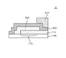
次に、発光装置10の製造方法について、図6を用いて説明する。まず、基板100上に第1電極110を形成する。この工程において、第1端子112及び第2端子132も形成される。次いで、絶縁層150、有機層120、及び第2電極130をこの順に形成する。 Next, a method for manufacturing the
次いで、図6に示すように、第1端子112及び第2端子132の上に、リフトオフ層220を形成する。リフトオフ層220は、例えば薬液や水によって除去される層であり、例えば可溶化したアクリル系樹脂である。リフトオフ層220の厚さは、例えば1μm以上5μm以下である。 Next, as shown in FIG. 6, a lift-
次いで、封止層200を、例えば、CVD法、スパッタリング法、ALD法などの成膜法を用いて形成する。このとき、封止層200は発光部140と重なる領域を含めて、基板100の第1面102のほぼ全面に形成される。このため、第1端子112及び第2端子132も封止層200で覆われる。 Next, the
次いで、封止層200の上に、被覆層210となる層を、例えば塗布法を用いて形成する。このとき、被覆層210となる層を、リフトオフ層220の少なくとも一部(例えばリフトオフ層220の縁のうち発光部140の近くに位置する領域)と重ねる。次いで、被覆層210を硬化させる。このとき、封止層200と被覆層210の間には応力が発生する。このため、封止層200のうちリフトオフ層220と重なる領域にはクラックが発生する。このクラックの一部は、封止層200のうちリフトオフ層220と重なっているが被覆層210で覆われていない部分にも生じる。特に、被覆層210が熱硬化型の樹脂で形成されている場合、この硬化工程において、封止層200と被覆層210の間には、これらを形成する材料の熱膨張率の差に起因して、熱応力が発生する。このため、封止層200のうちリフトオフ層220と重なる領域には、多くのクラックが発生する。 Next, a layer that becomes the
次いで、封止層200のうち第1端子112と重なる部分及び第2端子132と重なる部分を、リフトオフ層220を溶解させる液体(薬液又は水)で洗浄する。この液体は、封止層200に形成されたクラックを経由してリフトオフ層220に到達し、リフトオフ層220を溶解させる。これにより封止層200のうち第1端子112と重なる部分及び第2端子132と重なる部分は除去される。この際、被覆層210には突出部212が形成される。 Next, the portion of the
以上、本実施形態によれば、被覆層210となる層はリフトオフ層220の少なくとも一部と重なっている。このため、被覆層210を硬化させるときに、リフトオフ層220と被覆層210の間には応力が発生し、その結果、封止層200のうちリフトオフ層220の上に位置する部分にはクラックが発生する。従って、封止層200のうちリフトオフ層220の上に位置する部分、すなわち封止層200のうち第1端子112と重なる部分及び第2端子132と重なる部分を、容易に除去することができる。そしてこの結果、被覆層210には突出部212が形成される。 As described above, according to the present embodiment, the layer that becomes the
(変形例1)
図7は、変形例1に係る発光装置10の構成を示す断面図であり、第1の実施形態における図5に対応している。図8は、図7に示した発光装置10の製造方法を示す断面図であり、第1の実施形態における図6に対応している。(Modification 1)
FIG. 7 is a cross-sectional view illustrating a configuration of the
本変形例に係る発光装置10は、基板100のうち第1端子112の周囲に位置する領域の上に、封止層200が形成されている点を除いて、第1の実施形態に係る発光装置10と同様の構成である。言い換えると、封止層200のうち第1端子112と重なる領域及び第2端子132と重なる領域のそれぞれには、開口が形成されている。このようにするためには、例えば図8に示すように、リフトオフ層220の縁を基板100の縁から離せばよい。なお、第2端子132の近くも、図7と同様の構造を有していてもよい。 The
本変形例によっても、第1の実施形態と同様に、被覆層210を硬化させるときに、封止層200にはクラックが生じる。このため、リフトオフ層220の上に位置する封止層200を、容易にリフトオフさせることができる。 Also according to this modification, cracks are generated in the
(変形例2)
図9は、変形例2に係る発光装置10の構成を示す断面図であり、第1の実施形態における図5に対応している。本変形例に係る発光装置10は、第1端子112の端部の上に封止層200が形成されている点を除いて、変形例1に係る発光装置10と同様の構成である。このようにするためには、リフトオフ層220の縁を第1端子112の先端から離せばよい。なお、第2端子132の近くも、図9と同様の構造を有していてもよい。(Modification 2)
FIG. 9 is a cross-sectional view illustrating a configuration of the
本変形例によっても、第1の実施形態と同様に、被覆層210を硬化させるときに、封止層200にはクラックが生じる。このため、リフトオフ層220の上に位置する封止層200を、容易にリフトオフさせることができる。 Also according to this modification, cracks are generated in the
(変形例3)
図10は、変形例3に係る発光装置10の構成を示す断面図であり、第1の実施形態における図5に対応している。本変形例に係る発光装置10は、第1端子112が導体層160を備えている点を除いて、第1の実施形態、変形例1、又は変形例2に係る発光装置10と同様の構成である。なお、図10は、第1の実施形態と同様の場合を示している。(Modification 3)
FIG. 10 is a cross-sectional view illustrating a configuration of the
導体層160は、第1電極110から続く層の上に形成されており、第1電極110よりも抵抗が低い材料、例えば金属又は合金によって形成されている。導体層160が形成されることにより、第1端子112の抵抗は低くなる。なお、導体層160は、第1電極110の上にも形成されていてもよい。この場合、第1電極110の上には、複数の線状の導体層160が形成される。これらの導体層160は、第1電極110の補助電極として機能する。これにより、第1電極110の見かけ上の抵抗は低くなる。なお、導体層160は、多層構造を有していてもよい。例えば導体層160は、Mo又はMo合金からなる第1層、Al又はAl合金からなる第2層、及びMo又はMo合金からなる第3層をこの順に重ねた構成を有していてもよい。この場合、第1層及び第3層の厚さは、例えば40nm以上200nm以下である。また第2層の厚さは、例えば50nm以上1000nm以下である。 The
なお、第2端子132も本図に示した構成を有している。 The
本変形例によっても、第1の実施形態と同様に、被覆層210を硬化させるときに、封止層200にはクラックが生じる。このため、リフトオフ層220の上に位置する封止層200を、容易にリフトオフさせることができる。また、第1端子112の抵抗及び第2端子132の抵抗を低くすることができる。 Also according to this modification, cracks are generated in the
(第2の実施形態)
図11は、第2の実施形態に係る発光装置10の平面図である。図12は、図11から隔壁170、第2電極130、有機層120、及び絶縁層150を取り除いた図である。図13は図11のB−B断面図であり、図14は図11のC−C断面図であり、図15は図11のD−D断面図である。(Second Embodiment)
FIG. 11 is a plan view of the
本実施形態に係る発光装置10はディスプレイであり、基板100、第1電極110、発光部140、絶縁層150、複数の開口152、複数の開口154、複数の引出配線114、有機層120、第2電極130、複数の引出配線134、及び複数の隔壁170を有している。 The
第1電極110は、第1方向(図11におけるY方向)にライン状に延在している。そして第1電極110の端部は、引出配線114に接続している。 The
引出配線114は、第1電極110を第1端子112に接続する配線である。本図に示す例では、引出配線114の一端側は第1電極110に接続しており、引出配線114の他端側は第1端子112となっている。本図に示す例において、第1電極110及び引出配線114は一体になっている。そして引出配線114の上には、導体層160が形成されている。導体層160の構成は、変形例3と同様である。なお、引出配線114の一部は絶縁層150によって覆われている。 The
絶縁層150は、図11、及び図13〜図15に示すように、複数の第1電極110上及びその間の領域に形成されている。絶縁層150には、複数の開口152及び複数の開口154が形成されている。複数の第2電極130は、第1電極110と交差する方向(例えば直交する方向:図11におけるX方向)に互いに平行に延在している。そして、複数の第2電極130の間には、詳細を後述する隔壁170が延在している。開口152は、平面視で第1電極110と第2電極130の交点に位置している。具体的には、複数の開口152は、第1電極110が延在する方向(図11におけるY方向)に並んでいる。また、複数の開口152は、第2電極130の延在方向(図11におけるX方向)にも並んでいる。このため、複数の開口152はマトリクスを構成するように配置されていることになる。 As shown in FIGS. 11 and 13 to 15, the insulating
開口154は、平面視で複数の第2電極130のそれぞれの一端側と重なる領域に位置している。また開口154は、開口152が構成するマトリクスの一辺に沿って配置されている。そしてこの一辺に沿う方向(例えば図11におけるY方向、すなわち第1電極110に沿う方向)で見た場合、開口154は、所定の間隔で配置されている。開口154からは、引出配線134の一部分が露出している。そして、引出配線134は、開口154を介して第2電極130に接続している。 The
引出配線134は、第2電極130を第2端子132に接続する配線であり、第1電極110と同一の材料からなる層を有している。引出配線134の一端側は開口154の下に位置しており、引出配線134の他端側は、絶縁層150の外部に引き出されている。そして本図に示す例では、引出配線134の他端側が第2端子132となっている。そして引出配線134の上には、導体層160が形成されている。導体層160の構成は、変形例3と同様である。なお、引出配線134の一部は絶縁層150によって覆われている。 The
開口152と重なる領域には、有機層120が形成されている。有機層120の正孔注入層は第1電極110に接しており、有機層120の電子注入層は第2電極130に接している。このため、発光部140は、開口152と重なる領域それぞれに位置していることになる。 In the region overlapping with the
なお、図13及び図14に示す例では、有機層120を構成する各層は、いずれも開口152の外側まではみ出している場合を示している。そして図11に示すように、有機層120は、隔壁170が延在する方向において、隣り合う開口152の間にも連続して形成されていてもよいし、連続して形成していなくてもよい。ただし、図15に示すように、有機層120は、開口154には形成されていない。 In the example shown in FIGS. 13 and 14, the layers constituting the
第2電極130は、図11、図13〜図15に示すように、第1方向と交わる第2方向(図11におけるX方向)に延在している。そして隣り合う第2電極130の間には、隔壁170が形成されている。隔壁170は、第2電極130と平行すなわち第2方向に延在している。隔壁170の下地は、例えば絶縁層150である。隔壁170は、例えばポリイミド系樹脂などの感光性の樹脂であり、露光及び現像されることによって、所望のパターンに形成されている。なお、隔壁170はポリイミド系樹脂以外の樹脂、例えばエポキシ系樹脂やアクリル系樹脂、二酸化珪素等の無機材料で構成されていても良い。 As shown in FIGS. 11 and 13 to 15, the
隔壁170は、断面が台形の上下を逆にした形状(逆台形)になっている。すなわち隔壁170の上面の幅は、隔壁170の下面の幅よりも大きい。このため、隔壁170を第2電極130より前に形成しておくと、蒸着法やスパッタリング法を用いて、第2電極130を基板100の一面側に形成することで、複数の第2電極130を一括で形成することができる。また、隔壁170は、有機層120を分断する機能も有している。 The
そして本実施形態においても、発光装置10は封止層200および被覆層210を有している。封止層200および被覆層210の構成及びレイアウトは、第1の実施形態又はその変形例に示した通りである。ただし本実施形態では、第1端子112及び第2端子132は、基板100のうち同一の辺に沿って配置されている。このため、封止層200のうち第1端子112を露出するための開口と、第2端子132を露出するための開口は互いに繋がっている。 Also in this embodiment, the
次に、本実施形態における発光装置10の製造方法を説明する。まず、基板100上に第1電極110、引出配線114,134を形成する。これらの形成方法は、第1の実施形態と同様である。 Next, a method for manufacturing the
次いで、引出配線114上及び引出配線134上に、導体層160を形成する。次いで、絶縁層150を形成し、さらに隔壁170を形成する。次いで有機層120及び第2電極130を形成する。これらの形成方法は、第1の実施形態と同様である。 Next, the
そして、リフトオフ層220、封止層200、及び被覆層210をこの順に形成する。次いで、封止層200のうち第1端子112と重なる部分及び第2端子132と重なる部分を除去する。これらの工程は、第1の実施形態と同様である。 Then, the lift-
本実施形態によれば、発光部140を用いたディスプレイにおいて、第1の実施形態と同様に、封止層200のうち第1端子112の上に位置する部分及び第2端子132の上に位置する部分を容易に除去することができる。 According to the present embodiment, in the display using the
以上、図面を参照して実施形態について述べたが、これらは本発明の例示であり、上記以外の様々な構成を採用することもできる。 As mentioned above, although embodiment was described with reference to drawings, these are illustrations of this invention and various structures other than the above are also employable.
Claims (6)
Translated fromJapanese前記基板に形成された発光部と、
前記基板に形成され、前記発光部に電気的に接続する端子と、
前記基板に形成され、前記発光部を封止し、かつ前記端子を覆っていない封止層と、
前記封止層の上に形成され、前記封止層とは異なる材料によって形成されている被覆層と、
を備え、
前記端子の隣に位置する領域の少なくとも一部において、前記被覆層の端部は前記封止層の端部より外側にある発光装置。A substrate,
A light emitting part formed on the substrate;
A terminal formed on the substrate and electrically connected to the light emitting unit;
A sealing layer that is formed on the substrate, seals the light emitting portion, and does not cover the terminals;
A coating layer formed on the sealing layer and formed of a material different from the sealing layer;
With
The light emitting device in which an end portion of the covering layer is outside an end portion of the sealing layer in at least a part of a region located next to the terminal.
前記封止層は無機層であり、かつ前記封止層の厚さは300nm以下である発光装置。The light-emitting device according to claim 1.
The light-emitting device, wherein the sealing layer is an inorganic layer, and the thickness of the sealing layer is 300 nm or less.
前記被覆層は熱硬化型の樹脂層である発光装置。The light-emitting device according to claim 2.
The light emitting device, wherein the coating layer is a thermosetting resin layer.
前記被覆層は前記封止層よりも厚い発光装置。In the light-emitting device as described in any one of Claims 1-3,
The light-emitting device in which the coating layer is thicker than the sealing layer.
前記被覆層のうち前記封止層の外側に位置する部分は、前記封止層の下地に接していない発光装置。In the light-emitting device as described in any one of Claims 1-4,
A portion of the coating layer located outside the sealing layer is a light emitting device that is not in contact with the base of the sealing layer.
前記発光部は、第1電極、第2電極、及び前記第1電極と前記第2電極の間に位置する有機層と、
を備え、
前記端子は前記第1電極又は前記第2電極に接続している発光装置。In the light-emitting device as described in any one of Claims 1-5,
The light emitting unit includes a first electrode, a second electrode, and an organic layer positioned between the first electrode and the second electrode,
With
The light emitting device, wherein the terminal is connected to the first electrode or the second electrode.
Applications Claiming Priority (1)
| Application Number | Priority Date | Filing Date | Title |
|---|---|---|---|
| PCT/JP2014/081637WO2016084256A1 (en) | 2014-11-28 | 2014-11-28 | Light emitting device |
Related Child Applications (1)
| Application Number | Title | Priority Date | Filing Date |
|---|---|---|---|
| JP2018170748ADivisionJP6595066B2 (en) | 2018-09-12 | 2018-09-12 | Light emitting device manufacturing method and light emitting device |
Publications (2)
| Publication Number | Publication Date |
|---|---|
| JPWO2016084256A1true JPWO2016084256A1 (en) | 2017-08-03 |
| JP6404361B2 JP6404361B2 (en) | 2018-10-10 |
Family
ID=56073859
Family Applications (1)
| Application Number | Title | Priority Date | Filing Date |
|---|---|---|---|
| JP2016561204AActiveJP6404361B2 (en) | 2014-11-28 | 2014-11-28 | Light emitting device |
Country Status (3)
| Country | Link |
|---|---|
| US (4) | US10243165B2 (en) |
| JP (1) | JP6404361B2 (en) |
| WO (1) | WO2016084256A1 (en) |
Families Citing this family (3)
| Publication number | Priority date | Publication date | Assignee | Title |
|---|---|---|---|---|
| JP6404361B2 (en) | 2014-11-28 | 2018-10-10 | パイオニア株式会社 | Light emitting device |
| JP6595066B2 (en)* | 2018-09-12 | 2019-10-23 | パイオニア株式会社 | Light emitting device manufacturing method and light emitting device |
| KR20210018591A (en)* | 2019-08-06 | 2021-02-18 | 삼성디스플레이 주식회사 | Display device |
Citations (7)
| Publication number | Priority date | Publication date | Assignee | Title |
|---|---|---|---|---|
| JPH1140344A (en)* | 1997-07-16 | 1999-02-12 | Casio Comput Co Ltd | Electroluminescent element |
| JP2004079291A (en)* | 2002-08-13 | 2004-03-11 | Matsushita Electric Works Ltd | Organic electroluminescent element |
| JP2007080569A (en)* | 2005-09-12 | 2007-03-29 | Toyota Industries Corp | Method for manufacturing organic electroluminescence element |
| JP2012042662A (en)* | 2010-08-18 | 2012-03-01 | Denso Corp | Organic el display device |
| WO2014141463A1 (en)* | 2013-03-15 | 2014-09-18 | パイオニア株式会社 | Light emitting device and method for inspecting light emitting device |
| JP2014186169A (en)* | 2013-03-22 | 2014-10-02 | Toshiba Corp | Manufacturing method of display device and display device |
| JP2014197522A (en)* | 2012-05-09 | 2014-10-16 | 株式会社半導体エネルギー研究所 | Light-emitting device and electronic apparatus |
Family Cites Families (53)
| Publication number | Priority date | Publication date | Assignee | Title |
|---|---|---|---|---|
| JPS63105493A (en)* | 1986-10-22 | 1988-05-10 | アルプス電気株式会社 | Thin film el panel |
| US5189405A (en)* | 1989-01-26 | 1993-02-23 | Sharp Kabushiki Kaisha | Thin film electroluminescent panel |
| US5652067A (en)* | 1992-09-10 | 1997-07-29 | Toppan Printing Co., Ltd. | Organic electroluminescent device |
| US5811177A (en)* | 1995-11-30 | 1998-09-22 | Motorola, Inc. | Passivation of electroluminescent organic devices |
| US6195142B1 (en)* | 1995-12-28 | 2001-02-27 | Matsushita Electrical Industrial Company, Ltd. | Organic electroluminescence element, its manufacturing method, and display device using organic electroluminescence element |
| US5693956A (en)* | 1996-07-29 | 1997-12-02 | Motorola | Inverted oleds on hard plastic substrate |
| US6700692B2 (en)* | 1997-04-02 | 2004-03-02 | Gentex Corporation | Electrochromic rearview mirror assembly incorporating a display/signal light |
| KR100249784B1 (en)* | 1997-11-20 | 2000-04-01 | 정선종 | Packaging method of organic or polymer electroluminescent device using polymer composite membrane |
| CN1287636C (en)* | 1998-08-03 | 2006-11-29 | 杜邦显示器股份有限公司 | Light-emitting device with protective inorganic material encapsulation layer and method for protecting the device |
| US7126161B2 (en)* | 1998-10-13 | 2006-10-24 | Semiconductor Energy Laboratory Co., Ltd. | Semiconductor device having El layer and sealing material |
| JP4112779B2 (en)* | 2000-05-31 | 2008-07-02 | 三星エスディアイ株式会社 | Manufacturing method of organic EL element |
| US6924594B2 (en)* | 2000-10-03 | 2005-08-02 | Semiconductor Energy Laboratory Co., Ltd. | Light emitting device |
| KR100413450B1 (en)* | 2001-07-20 | 2003-12-31 | 엘지전자 주식회사 | protecting film structure for display device |
| JP4010394B2 (en)* | 2001-12-14 | 2007-11-21 | 大日本印刷株式会社 | Electroluminescent element |
| JP2004022291A (en)* | 2002-06-14 | 2004-01-22 | Nippon Sheet Glass Co Ltd | EL element sealing plate, mother glass substrate for multiple sealing plate sealing, and EL element |
| JP2004319530A (en)* | 2003-02-28 | 2004-11-11 | Sanyo Electric Co Ltd | Optical semiconductor device and method of manufacturing the same |
| JP2005116497A (en)* | 2003-03-10 | 2005-04-28 | Nippon Sheet Glass Co Ltd | Display panel and manufacturing method thereof |
| ATE476757T1 (en)* | 2004-10-21 | 2010-08-15 | Lg Display Co Ltd | ORGANIC ELECTROLUMINESCENT DEVICE AND METHOD OF PRODUCTION |
| US20060093795A1 (en)* | 2004-11-04 | 2006-05-04 | Eastman Kodak Company | Polymeric substrate having a desiccant layer |
| JP4696796B2 (en)* | 2005-09-07 | 2011-06-08 | 株式会社豊田自動織機 | Method for manufacturing organic electroluminescence device |
| JP4702009B2 (en)* | 2005-11-22 | 2011-06-15 | セイコーエプソン株式会社 | LIGHT EMITTING DEVICE AND ELECTRONIC DEVICE |
| KR100671647B1 (en)* | 2006-01-26 | 2007-01-19 | 삼성에스디아이 주식회사 | Organic light emitting display device |
| JP4776393B2 (en)* | 2006-02-20 | 2011-09-21 | 株式会社 日立ディスプレイズ | Organic EL display device |
| US8830695B2 (en)* | 2007-01-25 | 2014-09-09 | Osram Opto Semiconductors Gmbh | Encapsulated electronic device |
| JP2008192426A (en)* | 2007-02-02 | 2008-08-21 | Fujifilm Corp | Light emitting device |
| JP2008210788A (en)* | 2007-02-02 | 2008-09-11 | Toppan Printing Co Ltd | Organic EL device |
| US8415879B2 (en)* | 2007-05-31 | 2013-04-09 | Nthdegree Technologies Worldwide Inc | Diode for a printable composition |
| US7936122B2 (en)* | 2007-12-14 | 2011-05-03 | Canon Kabushiki Kaisha | Organic EL display apparatus |
| US20090289349A1 (en)* | 2008-05-21 | 2009-11-26 | Spatial Photonics, Inc. | Hermetic sealing of micro devices |
| KR20120024658A (en)* | 2009-06-11 | 2012-03-14 | 샤프 가부시키가이샤 | Organic el display device and method for producing the same |
| PL2513998T3 (en)* | 2009-12-18 | 2018-02-28 | Arcelormittal | Large area light emitting device comprising organic light emitting diodes |
| TWI432320B (en)* | 2010-08-09 | 2014-04-01 | Ind Tech Res Inst | Packaging film, package structure and forming method thereof |
| US8735874B2 (en)* | 2011-02-14 | 2014-05-27 | Semiconductor Energy Laboratory Co., Ltd. | Light-emitting device, display device, and method for manufacturing the same |
| JP4918633B1 (en)* | 2011-07-28 | 2012-04-18 | パイオニア株式会社 | ORGANIC ELECTROLUMINESCENT DEVICE AND METHOD FOR PRODUCING ORGANIC ELECTROLUMINESCENT DEVICE |
| KR101809659B1 (en)* | 2011-10-14 | 2017-12-18 | 삼성디스플레이 주식회사 | Organic light emitting diode display and method for manufacturing the same |
| US9853245B2 (en)* | 2011-10-14 | 2017-12-26 | Samsung Display Co., Ltd. | Organic light emitting diode display and method for manufacturing the same |
| JP2014086114A (en) | 2012-10-25 | 2014-05-12 | Toshiba Corp | Method of manufacturing magnetic recording medium and method of manufacturing micro pattern |
| KR102000043B1 (en)* | 2012-10-31 | 2019-07-15 | 엘지디스플레이 주식회사 | Organic light emitting display device and method of fabricating thereof |
| KR102082407B1 (en)* | 2013-04-03 | 2020-02-28 | 삼성디스플레이 주식회사 | Flexible substrate, flexible display device, and method for manufacturing flexible display device |
| JP6201411B2 (en)* | 2013-05-14 | 2017-09-27 | セイコーエプソン株式会社 | Electro-optical device, method of manufacturing electro-optical device, and electronic apparatus |
| CA2920820A1 (en)* | 2013-08-14 | 2015-02-19 | Jx Nippon Oil & Energy Corporation | Light emitting element and method for manufacturing light emitting element |
| KR102096054B1 (en)* | 2013-08-14 | 2020-04-02 | 삼성디스플레이 주식회사 | Display device and method of fabricating the same |
| EP2983223B1 (en)* | 2013-08-21 | 2018-11-14 | LG Display Co., Ltd. | Organic light-emitting device and method for manufacturing same |
| JP6282832B2 (en)* | 2013-10-01 | 2018-02-21 | 株式会社ジャパンディスプレイ | Organic EL display device |
| DE102013113190A1 (en)* | 2013-11-28 | 2015-05-28 | Osram Oled Gmbh | Electronic component |
| US9461214B2 (en)* | 2013-11-29 | 2016-10-04 | Nichia Corporation | Light emitting device with phosphor layer |
| KR20150083684A (en)* | 2014-01-10 | 2015-07-20 | 삼성디스플레이 주식회사 | Display device and fabrication method thereof |
| JP2015173078A (en)* | 2014-03-12 | 2015-10-01 | 株式会社ジャパンディスプレイ | Organic EL display device and organic EL display device manufacturing method |
| JP6515537B2 (en)* | 2014-04-08 | 2019-05-22 | セイコーエプソン株式会社 | Method of manufacturing organic EL device, organic EL device, electronic device |
| JP6404361B2 (en) | 2014-11-28 | 2018-10-10 | パイオニア株式会社 | Light emitting device |
| JP2016143606A (en)* | 2015-02-04 | 2016-08-08 | セイコーエプソン株式会社 | Organic EL device and electronic device |
| KR102511413B1 (en)* | 2015-12-15 | 2023-03-16 | 엘지디스플레이 주식회사 | Organic light emitting display device |
| JP6595066B2 (en) | 2018-09-12 | 2019-10-23 | パイオニア株式会社 | Light emitting device manufacturing method and light emitting device |
- 2014
- 2014-11-28JPJP2016561204Apatent/JP6404361B2/enactiveActive
- 2014-11-28WOPCT/JP2014/081637patent/WO2016084256A1/enactiveApplication Filing
- 2014-11-28USUS15/531,393patent/US10243165B2/enactiveActive
- 2019
- 2019-02-22USUS16/283,686patent/US11075355B2/enactiveActive
- 2021
- 2021-06-23USUS17/356,418patent/US11864409B2/enactiveActive
- 2023
- 2023-11-22USUS18/518,260patent/US20240099050A1/ennot_activeAbandoned
Patent Citations (7)
| Publication number | Priority date | Publication date | Assignee | Title |
|---|---|---|---|---|
| JPH1140344A (en)* | 1997-07-16 | 1999-02-12 | Casio Comput Co Ltd | Electroluminescent element |
| JP2004079291A (en)* | 2002-08-13 | 2004-03-11 | Matsushita Electric Works Ltd | Organic electroluminescent element |
| JP2007080569A (en)* | 2005-09-12 | 2007-03-29 | Toyota Industries Corp | Method for manufacturing organic electroluminescence element |
| JP2012042662A (en)* | 2010-08-18 | 2012-03-01 | Denso Corp | Organic el display device |
| JP2014197522A (en)* | 2012-05-09 | 2014-10-16 | 株式会社半導体エネルギー研究所 | Light-emitting device and electronic apparatus |
| WO2014141463A1 (en)* | 2013-03-15 | 2014-09-18 | パイオニア株式会社 | Light emitting device and method for inspecting light emitting device |
| JP2014186169A (en)* | 2013-03-22 | 2014-10-02 | Toshiba Corp | Manufacturing method of display device and display device |
Also Published As
| Publication number | Publication date |
|---|---|
| US10243165B2 (en) | 2019-03-26 |
| US20210328170A1 (en) | 2021-10-21 |
| JP6404361B2 (en) | 2018-10-10 |
| US11075355B2 (en) | 2021-07-27 |
| US11864409B2 (en) | 2024-01-02 |
| WO2016084256A1 (en) | 2016-06-02 |
| US20190207142A1 (en) | 2019-07-04 |
| US20240099050A1 (en) | 2024-03-21 |
| US20170346034A1 (en) | 2017-11-30 |
Similar Documents
| Publication | Publication Date | Title |
|---|---|---|
| CN110462565B (en) | Display device with built-in touch sensor | |
| US20240099050A1 (en) | Light-emitting device | |
| JP6595066B2 (en) | Light emitting device manufacturing method and light emitting device | |
| JP2016095990A (en) | Light emitting device | |
| JP2022164806A (en) | Light-emitting device | |
| JP2016119201A (en) | Light-emitting device | |
| JP2017123238A (en) | Light-emitting device | |
| JP2020013797A (en) | Light emitting device manufacturing method | |
| JP7390508B2 (en) | Light-emitting device and method for manufacturing the light-emitting device | |
| JP6499876B2 (en) | Light emitting device | |
| JPWO2017163331A1 (en) | LIGHT EMITTING DEVICE, ELECTRONIC DEVICE, AND METHOD FOR MANUFACTURING LIGHT EMITTING DEVICE | |
| JP6580336B2 (en) | Light emitting device | |
| JP2016095991A (en) | Light emission device | |
| JPWO2017119068A1 (en) | Light emitting device | |
| JP2019201004A (en) | Light-emitting device | |
| JP2023171394A (en) | Light emission device | |
| JP2016178061A (en) | Light emitting device manufacturing method | |
| JP6496138B2 (en) | Light emitting device | |
| JP2016149315A (en) | Manufacturing method for light-emitting device | |
| JP2016181426A (en) | Light-emitting device | |
| JP2019192662A (en) | Light-emitting device | |
| JP2016100172A (en) | Light-emitting device and method for manufacturing light-emitting device | |
| JP2016184545A (en) | Light emission device and light emission system | |
| JP2016143529A (en) | Light emission device | |
| JP2016149226A (en) | Light-emitting device |
Legal Events
| Date | Code | Title | Description |
|---|---|---|---|
| A521 | Request for written amendment filed | Free format text:JAPANESE INTERMEDIATE CODE: A523 Effective date:20170329 | |
| A621 | Written request for application examination | Free format text:JAPANESE INTERMEDIATE CODE: A621 Effective date:20170329 | |
| A131 | Notification of reasons for refusal | Free format text:JAPANESE INTERMEDIATE CODE: A131 Effective date:20180123 | |
| A521 | Request for written amendment filed | Free format text:JAPANESE INTERMEDIATE CODE: A523 Effective date:20180322 | |
| TRDD | Decision of grant or rejection written | ||
| A01 | Written decision to grant a patent or to grant a registration (utility model) | Free format text:JAPANESE INTERMEDIATE CODE: A01 Effective date:20180814 | |
| A61 | First payment of annual fees (during grant procedure) | Free format text:JAPANESE INTERMEDIATE CODE: A61 Effective date:20180912 | |
| R150 | Certificate of patent or registration of utility model | Ref document number:6404361 Country of ref document:JP Free format text:JAPANESE INTERMEDIATE CODE: R150 |