JPWO2016056434A1 - Transparent conductor, method for producing transparent conductor, and touch panel - Google Patents
Transparent conductor, method for producing transparent conductor, and touch panelDownload PDFInfo
- Publication number
- JPWO2016056434A1 JPWO2016056434A1JP2016553056AJP2016553056AJPWO2016056434A1JP WO2016056434 A1JPWO2016056434 A1JP WO2016056434A1JP 2016553056 AJP2016553056 AJP 2016553056AJP 2016553056 AJP2016553056 AJP 2016553056AJP WO2016056434 A1JPWO2016056434 A1JP WO2016056434A1
- Authority
- JP
- Japan
- Prior art keywords
- transparent conductor
- fine particles
- metal fine
- convex portions
- ionic liquid
- Prior art date
- Legal status (The legal status is an assumption and is not a legal conclusion. Google has not performed a legal analysis and makes no representation as to the accuracy of the status listed.)
- Pending
Links
Images


Classifications
- H—ELECTRICITY
- H01—ELECTRIC ELEMENTS
- H01B—CABLES; CONDUCTORS; INSULATORS; SELECTION OF MATERIALS FOR THEIR CONDUCTIVE, INSULATING OR DIELECTRIC PROPERTIES
- H01B1/00—Conductors or conductive bodies characterised by the conductive materials; Selection of materials as conductors
- H01B1/20—Conductive material dispersed in non-conductive organic material
- H01B1/22—Conductive material dispersed in non-conductive organic material the conductive material comprising metals or alloys
- G—PHYSICS
- G02—OPTICS
- G02B—OPTICAL ELEMENTS, SYSTEMS OR APPARATUS
- G02B1/00—Optical elements characterised by the material of which they are made; Optical coatings for optical elements
- G02B1/10—Optical coatings produced by application to, or surface treatment of, optical elements
- G02B1/11—Anti-reflection coatings
- G02B1/118—Anti-reflection coatings having sub-optical wavelength surface structures designed to provide an enhanced transmittance, e.g. moth-eye structures
- G—PHYSICS
- G06—COMPUTING OR CALCULATING; COUNTING
- G06F—ELECTRIC DIGITAL DATA PROCESSING
- G06F3/00—Input arrangements for transferring data to be processed into a form capable of being handled by the computer; Output arrangements for transferring data from processing unit to output unit, e.g. interface arrangements
- G06F3/01—Input arrangements or combined input and output arrangements for interaction between user and computer
- G06F3/03—Arrangements for converting the position or the displacement of a member into a coded form
- G06F3/041—Digitisers, e.g. for touch screens or touch pads, characterised by the transducing means
- G06F3/044—Digitisers, e.g. for touch screens or touch pads, characterised by the transducing means by capacitive means
- G06F3/0446—Digitisers, e.g. for touch screens or touch pads, characterised by the transducing means by capacitive means using a grid-like structure of electrodes in at least two directions, e.g. using row and column electrodes
- H—ELECTRICITY
- H01—ELECTRIC ELEMENTS
- H01B—CABLES; CONDUCTORS; INSULATORS; SELECTION OF MATERIALS FOR THEIR CONDUCTIVE, INSULATING OR DIELECTRIC PROPERTIES
- H01B13/00—Apparatus or processes specially adapted for manufacturing conductors or cables
- H01B13/30—Drying; Impregnating
- G—PHYSICS
- G06—COMPUTING OR CALCULATING; COUNTING
- G06F—ELECTRIC DIGITAL DATA PROCESSING
- G06F2203/00—Indexing scheme relating to G06F3/00 - G06F3/048
- G06F2203/041—Indexing scheme relating to G06F3/041 - G06F3/045
- G06F2203/04103—Manufacturing, i.e. details related to manufacturing processes specially suited for touch sensitive devices
- G—PHYSICS
- G06—COMPUTING OR CALCULATING; COUNTING
- G06F—ELECTRIC DIGITAL DATA PROCESSING
- G06F2203/00—Indexing scheme relating to G06F3/00 - G06F3/048
- G06F2203/041—Indexing scheme relating to G06F3/041 - G06F3/045
- G06F2203/04112—Electrode mesh in capacitive digitiser: electrode for touch sensing is formed of a mesh of very fine, normally metallic, interconnected lines that are almost invisible to see. This provides a quite large but transparent electrode surface, without need for ITO or similar transparent conductive material
- G—PHYSICS
- G06—COMPUTING OR CALCULATING; COUNTING
- G06F—ELECTRIC DIGITAL DATA PROCESSING
- G06F3/00—Input arrangements for transferring data to be processed into a form capable of being handled by the computer; Output arrangements for transferring data from processing unit to output unit, e.g. interface arrangements
- G06F3/01—Input arrangements or combined input and output arrangements for interaction between user and computer
- G06F3/03—Arrangements for converting the position or the displacement of a member into a coded form
- G06F3/041—Digitisers, e.g. for touch screens or touch pads, characterised by the transducing means
- G06F3/0412—Digitisers structurally integrated in a display
Landscapes
- Engineering & Computer Science (AREA)
- Physics & Mathematics (AREA)
- General Engineering & Computer Science (AREA)
- Theoretical Computer Science (AREA)
- General Physics & Mathematics (AREA)
- Human Computer Interaction (AREA)
- Chemical & Material Sciences (AREA)
- Dispersion Chemistry (AREA)
- Spectroscopy & Molecular Physics (AREA)
- Optics & Photonics (AREA)
- Manufacturing & Machinery (AREA)
- Non-Insulated Conductors (AREA)
- Laminated Bodies (AREA)
- Surface Treatment Of Optical Elements (AREA)
- Shielding Devices Or Components To Electric Or Magnetic Fields (AREA)
Abstract
Translated fromJapaneseDescription
Translated fromJapanese本発明は、透明導電体、透明導電体の製造方法、及び、タッチパネルに関する。より詳しくは、ディスプレイ分野のタッチパネル等で好適に用いられる透明導電体、上記透明導電体の製造方法、及び、上記透明導電体を備えるタッチパネルに関するものである。The present invention relates to a transparent conductor, a method for producing a transparent conductor, and a touch panel. More specifically, the present invention relates to a transparent conductor suitably used in a touch panel or the like in the display field, a method for producing the transparent conductor, and a touch panel including the transparent conductor.
透明導電体は、例えば、ディスプレイ分野のタッチパネル等において、主に透明電極として用いられている。一般的な透明導電体としては、インジウムスズ酸化物(ITO:Indium Tin Oxide)等の透明膜が広く用いられている。しかしながら、例えば、ITO膜には、下記(1)〜(4)のような問題があった。
(1)ITO膜の膜厚にバラツキがあると、ITO膜の表面及び裏面での反射光が干渉することによって、色付きが発生してしまう。
(2)ITO膜は、屈折率が1.9〜2.0程度であり、空気層との間の屈折率差が大きいため反射率が高い。
(3)タッチパネル等において複数のITO膜を用いる場合、その透過率(透明性)が低下してしまう。
(4)ITO膜の主原料であるインジウムが希少な金属であるため、その枯渇が危惧されている。The transparent conductor is mainly used as a transparent electrode in, for example, a touch panel in the display field. As a general transparent conductor, a transparent film such as indium tin oxide (ITO) is widely used. However, for example, the ITO film has the following problems (1) to (4).
(1) If there is variation in the film thickness of the ITO film, the reflected light on the front and back surfaces of the ITO film interferes and coloration occurs.
(2) The ITO film has a refractive index of about 1.9 to 2.0, and has a high refractive index because of a large refractive index difference from the air layer.
(3) When a plurality of ITO films are used in a touch panel or the like, the transmittance (transparency) is lowered.
(4) Since indium, which is the main raw material of the ITO film, is a rare metal, its depletion is a concern.
そこで、ITO膜に代えて、金属微粒子をパターン化して配置した透明導電体や、金属薄膜をパターニングした透明導電体等を利用することが提案されている(例えば、特許文献1〜16参照)。このような構成は、透明導電体による導電性に加えて、透明導電体の開口領域による透明性(光透過性)を有する、とされている。Therefore, it has been proposed to use a transparent conductor in which metal fine particles are arranged in a pattern, a transparent conductor in which a metal thin film is patterned, or the like instead of the ITO film (see, for example, Patent Documents 1 to 16). Such a configuration is supposed to have transparency (light transmittance) due to the opening region of the transparent conductor in addition to the conductivity by the transparent conductor.
更に、ナノメートルサイズの凹凸構造(ナノ構造)の一種である、モスアイ構造(蛾の目状の構造)を有する反射防止フィルム上に、ITO等の透明膜が形成された構成が提案されている(例えば、特許文献17参照)。このような構成は、ITO膜による導電性に加えて、モスアイ構造による低反射性を有する、とされている。また、透明導電体を形成する目的ではないが、モスアイ構造による低反射性に加えて、防汚性を有する構成(例えば、特許文献18参照)や、撥水性を有する構成(例えば、特許文献19参照)も提案されている。Furthermore, a configuration is proposed in which a transparent film such as ITO is formed on an antireflection film having a moth-eye structure (an eye-like structure), which is a kind of a nanometer-sized uneven structure (nanostructure). (For example, refer to Patent Document 17). Such a configuration is said to have low reflectivity due to the moth-eye structure in addition to the conductivity due to the ITO film. Moreover, although it is not the objective of forming a transparent conductor, in addition to the low reflectivity by a moth eye structure, the structure which has antifouling property (for example, refer patent document 18), and the structure which has water repellency (for example, patent document 19) See also).
しかしながら、従来の透明導電体では、導電性、透明性、及び、低反射性が充分ではなく、更に、モアレ等の発生によって品位が低下してしまうことがあった。However, conventional transparent conductors do not have sufficient conductivity, transparency, and low reflectivity, and the quality may deteriorate due to the occurrence of moire or the like.
上記特許文献1は、金属微粒子をパターン化して配置した透明導電体を開示している。しかしながら、上記特許文献1に記載の発明では、下記(A)〜(D)のような問題があり、改善の余地があった。上記特許文献2〜5についても同様であった。
(A)導電部として、マイクロメートルサイズのピッチを有する網目状構造を形成することが限界であり、表示装置と組み合わせて用いる場合は、このような網目状構造と表示素子の画素のパターン(マイクロメートルサイズの格子状構造)とが干渉し、モアレが発生してしまう。
(B)リング状のパターンに金属微粒子が凝集しやすいため、リング状のパターンを連結する部分において、金属微粒子の量が少なくなり、断線が発生しやすくなる。よって、導電部全体の抵抗率が高くなり、導電性が低下してしまう。
(C)導電部が基板上で凸部となっているため、外力によって取れやすく、耐久性が低い。
(D)透明基板上に網目状の導電部が形成された構成であるため、低反射性を有しない。Patent Document 1 discloses a transparent conductor in which metal fine particles are arranged in a pattern. However, the invention described in Patent Document 1 has the following problems (A) to (D), and there is room for improvement. The same applies to
(A) As a conductive portion, it is a limit to form a mesh structure having a pitch of micrometer size, and when used in combination with a display device, such a mesh structure and a pixel pattern of a display element (micrometer Moire occurs due to interference with the metric size lattice structure).
(B) Since the metal fine particles easily aggregate in the ring-shaped pattern, the amount of the metal fine particles is reduced at the portion where the ring-shaped pattern is connected, and disconnection is likely to occur. Therefore, the resistivity of the entire conductive portion is increased, and the conductivity is reduced.
(C) Since the conductive portion is a convex portion on the substrate, it can be easily removed by an external force and has low durability.
(D) Since it is the structure by which the mesh-shaped electroconductive part was formed on the transparent substrate, it does not have low reflectivity.
上記特許文献6は、透明基板上の金属薄膜をパターニングして導電部を形成する方法を開示している。しかしながら、上記特許文献6に記載の発明では、下記(E)〜(H)のような問題があり、改善の余地があった。上記特許文献7についても同様であった。
(E)導電部のパターンのピッチがマイクロメートルサイズであるため、表示装置と組み合わせて用いる場合は、このような導電部のパターンと表示素子の画素のパターン(マイクロメートルサイズの格子状構造)とが干渉し、モアレが発生してしまう。
(F)パターニングする際に、所定の大きさのフォトマスクを繋ぎ合わせて用いるため、その継ぎ目の境界がムラとして見えやすくなり、品位が低下してしまう。
(G)導電部が透明基板上で凸部となっているため、外力によって取れやすく、耐久性が低い。
(H)透明基板上で金属薄膜がパターニングされた構成であるため、低反射性を有しない。
(E) Since the pitch of the pattern of the conductive portion is a micrometer size, when used in combination with a display device, such a pattern of the conductive portion and a pixel pattern of the display element (micrometer-size lattice structure) Interfere with each other and moire occurs.
(F) When patterning, since photomasks of a predetermined size are connected and used, the boundary between the joints is easily seen as unevenness, and the quality is lowered.
(G) Since the conductive part is a convex part on the transparent substrate, it can be easily removed by an external force and has low durability.
(H) Since the metal thin film is patterned on the transparent substrate, it does not have low reflectivity.
上記特許文献8は、金属微粒子をパターン化して配置した透明導電体を開示している。しかしながら、上記特許文献8に記載の発明では、下記(I)〜(K)のような問題があり、改善の余地があった。上記特許文献9〜16についても同様であった。
(I)基板上での相分離を利用して導電部を形成するため、基板の表面状態を均一に保つ必要があり、工程管理が難しい。基板の表面状態が、汚れ、傷、異物等によって変化すると、金属微粒子の分布が不均一となり、網目のピッチ(マイクロメートルサイズ)が部分的に大きくなるため、ざらつきとして視認されてしまう。
(J)導電部が基板上で凸部となっているため、外力によって取れやすく、耐久性が低い。また、金属微粒子、バインダー、及び、溶媒を混合した溶液を基板に塗布し、乾燥工程で相分離させて導電部を形成する方法では、金属微粒子がわずかな量のバインダーによって基板に密着されているだけであるため、外力に弱い。
(K)基板上に網目状の導電部が形成された構成であるため、低反射性を有しない。
(I) Since the conductive portion is formed by utilizing phase separation on the substrate, it is necessary to keep the surface state of the substrate uniform, and process management is difficult. When the surface state of the substrate changes due to dirt, scratches, foreign matter, etc., the distribution of the metal fine particles becomes non-uniform and the mesh pitch (micrometer size) is partially increased, so that it is visually recognized as rough.
(J) Since the conductive part is a convex part on the substrate, it can be easily removed by an external force and has low durability. In the method of forming a conductive part by applying a mixed solution of metal fine particles, a binder, and a solvent to a substrate and performing phase separation in a drying process, the metal fine particles are adhered to the substrate with a slight amount of binder. Because it is only weak to external force.
(K) Since the structure has a mesh-like conductive portion formed on the substrate, it does not have low reflectivity.
上記特許文献17は、モスアイ構造を有する反射防止フィルム上に、ITO等の透明膜が形成された透明導電体を開示している。しかしながら、上記特許文献17に記載の発明では、ITO等の透明膜を用いているため、上記(1)〜(4)で既に説明した問題があり、改善の余地があった。Patent Document 17 discloses a transparent conductor in which a transparent film such as ITO is formed on an antireflection film having a moth-eye structure. However, in the invention described in Patent Document 17, since a transparent film such as ITO is used, there are problems already described in (1) to (4) above, and there is room for improvement.
上記特許文献18は、モスアイ構造を構成する凸部の間隙に、所定の屈折率を有するナノ粒子が充填された構成を開示している。しかしながら、上記特許文献18に記載の発明は、透明導電体を形成するためのものではなく、更に、下記(L)及び(M)のような問題があり、改善の余地があった。
(L)モスアイ構造を構成する凸部の間隙の屈折率が、空気に対して大きくなるため、反射率が大きくなってしまう。
(M)ナノ粒子はシリカ等の透明粒子であり、金属微粒子ではないため、導電性が充分ではない。
上記特許文献19に記載の発明も、透明導電体を形成するためのものではなく、導電性が充分ではなかった。Patent Document 18 discloses a configuration in which nanoparticles having a predetermined refractive index are filled in the gaps between convex portions constituting the moth-eye structure. However, the invention described in Patent Document 18 is not for forming a transparent conductor, and has the following problems (L) and (M), and there is room for improvement.
(L) Since the refractive index of the gap between the convex portions constituting the moth-eye structure is increased with respect to air, the reflectance is increased.
(M) Nanoparticles are transparent particles such as silica, and are not metal fine particles, and therefore have insufficient conductivity.
The invention described in Patent Document 19 is not for forming a transparent conductor, and the conductivity is not sufficient.
本発明は、上記現状に鑑みてなされたものであり、導電性、透明性、及び、低反射性に優れ、かつ、モアレ等の発生がない透明導電体と、上記透明導電体の製造方法と、上記透明導電体を備えるタッチパネルとを提供することを目的とするものである。The present invention has been made in view of the above situation, and is excellent in conductivity, transparency, and low reflectivity, and has no generation of moire, etc., and a method for producing the transparent conductor, It aims at providing a touch panel provided with the above-mentioned transparent conductor.
本発明者らは、導電性、透明性、及び、低反射性に優れ、かつ、モアレ等の発生がない透明導電体について種々検討したところ、モスアイ構造を有する反射防止フィルムと金属微粒子とを組み合わせた構成とすることに着目した。そして、モスアイ構造を構成する凸部の間隙の底部に金属微粒子を充填し、網目状の導電部を構成することを見出した。これにより、金属微粒子が構成する網目状の導電部で優れた導電性を示し、金属微粒子が充填されていない領域で優れた透明性(光透過性)を示し、モスアイ構造を有する反射防止フィルムで優れた低反射性を示すことができることを見出した。更に、このような構成とすることで、モアレ等の発生による品位低下を防止することができることを見出した。これにより、上記課題をみごとに解決することができることに想到し、本発明に到達したものである。The inventors of the present invention have conducted various studies on transparent conductors that are excellent in conductivity, transparency, and low reflectivity, and that do not generate moiré or the like. As a result, the antireflection film having a moth-eye structure and metal fine particles are combined. We focused on the configuration. Then, the inventors have found that the bottom of the gap between the convex portions constituting the moth-eye structure is filled with metal fine particles to constitute a network-like conductive portion. This is an antireflection film having a moth-eye structure that exhibits excellent conductivity in a mesh-like conductive portion composed of metal fine particles, and exhibits excellent transparency (light transmission) in a region not filled with metal fine particles. It was found that excellent low reflectivity can be exhibited. Furthermore, it has been found that such a configuration can prevent deterioration in quality due to the occurrence of moire or the like. Thus, the inventors have conceived that the above problems can be solved brilliantly and have reached the present invention.
すなわち、本発明の一態様は、複数の凸部が可視光の波長以下のピッチで、表面に設けられた反射防止フィルムと、上記複数の凸部の上記ピッチ以下の粒径を有し、かつ、上記複数の凸部の間隙の底部に充填された金属微粒子とを備え、上記複数の凸部の間隙に配置された上記金属微粒子は、網目状の導電部を構成するものである透明導電体であってもよい。That is, according to one embodiment of the present invention, the plurality of convex portions have a pitch equal to or smaller than the wavelength of visible light, the antireflection film provided on the surface, and the plurality of convex portions have a particle size equal to or smaller than the pitch, and A transparent conductor comprising: metal fine particles filled in the bottoms of the gaps of the plurality of convex parts, wherein the metal fine particles arranged in the gaps of the plurality of convex parts constitute a network-like conductive part It may be.
本発明の別の一態様は、上記透明導電体の製造方法であって、溶媒中に上記金属微粒子が分散された分散液を、上記反射防止フィルム上に塗布する工程(1)、塗布された上記分散液に対して上記溶媒を蒸発させる乾燥を行う工程(2)、及び、乾燥された上記分散液に対して加熱を行う工程(3)を含む透明導電体の製造方法であってもよい。Another aspect of the present invention is a method for producing the transparent conductor, the step (1) of applying a dispersion liquid in which the metal fine particles are dispersed in a solvent on the antireflection film. The transparent conductor manufacturing method may include a step (2) of drying the solvent to evaporate the solvent and a step (3) of heating the dried dispersion. .
本発明の更に別の一態様は、上記透明導電体を備えるタッチパネルであってもよい。Yet another embodiment of the present invention may be a touch panel including the transparent conductor.
本発明によれば、導電性、透明性、及び、低反射性に優れ、かつ、モアレ等の発生がない透明導電体と、上記透明導電体の製造方法と、上記透明導電体を備えるタッチパネルとを提供することができる。According to the present invention, a transparent conductor that is excellent in conductivity, transparency, and low reflectivity and does not generate moire, a method for producing the transparent conductor, and a touch panel that includes the transparent conductor; Can be provided.
以下に実施形態(実施例)を掲げ、本発明について図面を参照して更に詳細に説明するが、本発明はこれらの実施形態(実施例)のみに限定されるものではない。また、各実施形態(各実施例)の構成は、本発明の要旨を逸脱しない範囲において適宜組み合わされてもよいし、変更されてもよい。Embodiments (Examples) are listed below, and the present invention will be described in more detail with reference to the drawings. However, the present invention is not limited only to these embodiments (Examples). The configurations of the respective embodiments (each example) may be appropriately combined or changed within a range not departing from the gist of the present invention.
[実施形態1]
実施形態1は、反射防止フィルムと、金属微粒子とを備える透明導電体に関する。[Embodiment 1]
Embodiment 1 relates to a transparent conductor comprising an antireflection film and metal fine particles.
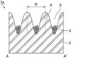
(1)透明導電体の構造
実施形態1の透明導電体の構造について、図1及び図2を参照して説明する。図1は、実施形態1の透明導電体を示す平面模式図である。図2は、図1中の線分A−A’に対応する部分の断面を示す断面模式図である。図1及び図2に示すように、透明導電体1aは、反射防止フィルム2、及び、金属微粒子3を備えている。反射防止フィルム2は、複数の凸部(突起)4が可視光の波長以下のピッチ(隣接する凸部4の頂点間の距離)Pで、表面に設けられた反射防止フィルム、すなわち、モスアイ構造(蛾の目状の構造)を有する反射防止フィルムに相当する。金属微粒子3は、モスアイ構造を構成する凸部4のピッチP以下の粒径を有し、かつ、凸部4の間隙5の底部に充填されており、網目状の導電部を構成している。本明細書中、凸部4の間隙5の底部は、凸部4の間隙5の深さの0%以上、50%以下の範囲を示す。なお、図1及び図2では、モスアイ構造や網目状の導電部(金属微粒子3)を拡大して明示している。実際の透明導電体1aでは、透明導電体1aの面積に対して、凸部4、及び、金属微粒子3の大きさが極めて小さい(可視光の波長に比べて小さい)ため、図1及び図2に示したように、モスアイ構造や網目状の導電部(金属微粒子3)を肉眼や光学顕微鏡等の光学的手段で識別することはできない。(1) Structure of transparent conductor The structure of the transparent conductor of Embodiment 1 will be described with reference to FIGS. FIG. 1 is a schematic plan view showing a transparent conductor of Embodiment 1. FIG. FIG. 2 is a schematic cross-sectional view showing a cross section of a portion corresponding to a line segment AA ′ in FIG. As shown in FIGS. 1 and 2, the
凸部4の形状は、先端に向かって細くなる形状であれば特に限定されず、例えば、柱状の下部と半球状の上部とによって構成される形状(以下、「釣鐘状」とも言う。)や、錐体状(コーン状、円錐状)等が挙げられる。また、凸部4は、枝突起を有する形状であってもよい。枝突起とは、モスアイ構造を形成するための陽極酸化及びエッチングを行う過程で、他の部分よりも特に不規則な間隔で形成されてしまった、図1に示すような凸部(枝突起13)を示す。金属微粒子3が充填されていない領域をより広くし、透明性をより高める観点からは、凸部4の形状として、図2に示すような、凸部4が下方に向かって太くなり、凸部4の間隙5の底部が狭い釣鐘状が好ましい。図2中、凸部4の間隙5の底辺は傾斜した形状となっているが、傾斜せずに水平な形状であってもよい。また、金属微粒子3が充填される領域をより広くし、導電性をより高める観点からは、凸部4の形状として、凸部4の間隙5の底部が広い形状が好ましい。The shape of the
凸部4のピッチPとしては、可視光の波長(780nm)以下であれば特に限定されないが、モアレ等の光学現象を充分に防止する観点からは、100nm以上、400nm以下であることが好ましく、100nm以上、200nm以下であることがより好ましい。本明細書中、凸部4のピッチPは、測定機として日立製作所社製の走査型電子顕微鏡(SEM:Scanning Electron Microscope、商品名:S−4700)を用い、SEM写真(平面写真)から読み取った、1μm□(角)の領域内における、枝突起を除くすべての隣接する凸部間の距離の平均値を示す。The pitch P of the
凸部4の高さは、金属微粒子3が凸部4の間隙5の外に出ないように設定されれば特に限定されず、50nm以上であることが好ましい。更に、凸部4の高さとしては、後述する凸部4の好適なアスペクト比と両立させる観点から、50nm以上、600nm以下であることが好ましく、100nm以上、300nm以下であることがより好ましい。本明細書中、凸部4の高さは、測定機として日立製作所社製のSEM(商品名:S−4700)を用い、SEM写真(断面写真)から読み取った、枝突起を除く連続して並んだ10個の凸部の高さの平均値を示す。ただし、10個の凸部を選択する際は、欠損や変形した部分(SEM写真用の試料を準備する際に変形させてしまった部分等)がある凸部を除くものとする。SEM写真用の試料としては、反射防止フィルムの特異的な欠陥がない領域でサンプリングされたものが用いられ、例えば、連続的に製造されるロール状の反射防止フィルムでは、その中央付近でサンプリングされたものを用いる。The height of the
凸部4のアスペクト比は特に限定されないが、モスアイ構造の加工性の観点からは、1.5以下であることが好ましい。凸部4のアスペクト比が大き過ぎる(凸部4が細長い)と、スティッキングが発生したり、モスアイ構造を形成する際の転写具合が悪化したりする(モスアイ構造の雌型が詰まったり、巻き付いてしまう、等)懸念がある。更に、凸部4のアスペクト比としては、モアレ等の光学現象を充分に防止し、良好な反射率特性を実現する観点からは、0.8以上、1.5以下であることが好ましい。本明細書中、凸部4のアスペクト比は、測定機として日立製作所社製のSEM(商品名:S−4700)を用い、上述したような方法で測定された凸部4のピッチPと高さとの比(高さ/ピッチP)で示す。Although the aspect ratio of the
凸部4の配置は特に限定されず、ランダムに配置されていても、規則的に配置されていてもよいが、モアレの発生を充分に防止する観点からは、図1に示すように、ランダムに配置されていることが好ましい。The arrangement of the
以上のような凸部4を形成する観点から、凸部4の材質としては、樹脂が好ましい。また、実施形態1の透明導電体を製造する際に反射防止フィルム2上に塗布する、金属微粒子3が分散された分散液の溶媒としては、一般的に、水、エタノール、アルコール系、エステル系等の極性溶媒が用いられるため、凸部4の材質としては、濡れ性が良好な親水性の樹脂がより好ましい。凸部4の材質として疎水性の樹脂を用いる場合、モスアイ構造によるロータス効果も合わさって、凸部4の間隙5に分散液を上手く塗布することができない懸念がある。From the viewpoint of forming the
金属微粒子3としては、導電性をより高める観点からは、低抵抗率を有する金属群の中から適宜選択することが好ましく、例えば、金、銀、銅、白金、アルミニウム等が挙げられる。中でも、抵抗率が非常に低い、金、銀、及び、銅の中から選択して用いることが好ましい。金属微粒子3としては、これらの金属群の中から1種類のみを用いてもよいし、複数種類を組み合わせて用いてもよい。また、これらの金属の合金を用いてもよい。The
金属微粒子3の形状は特に限定されず、例えば、球状、柱状(ファイバー状)、楕円球体状等が挙げられる。金属微粒子3が効率的に充填される観点からは、金属微粒子3の形状として、図2に示すような球状であることが好ましい。The shape of the
金属微粒子3の粒径は、凸部4のピッチP以下であれば特に限定されないが、金属微粒子3が効率的に充填される観点からは、50nm以下であることが好ましく、20nm以下であることがより好ましい。また、金属微粒子3がより効率的に充填される観点からは、粒径と同じ大きさの分布(金属微粒子3間の距離)を有するものを用いることが好ましい。本明細書中、金属微粒子3の粒径は、測定機として日立製作所社製のSEM(商品名:S−4700)を用い、SEM写真(平面写真及び断面写真)から読み取った、20個の金属微粒子の粒径の平均値を示す。ただし、20個の金属微粒子を選択する際は、欠損や変形した部分がある金属微粒子を除くものとする。本明細書中、粒径とは、金属微粒子3の全方向の長さの中で最大の長さを示す。例えば、金属微粒子3の形状が球状である場合は、その直径に相当する長さを示し、金属微粒子3の形状が楕円球体状である場合は、主軸、及び、主軸に垂直な方向の直径のうちでより長い方の長さを示す。導電性を充分に高め、透明性(透過率)の低下を充分に抑制する観点からは、金属微粒子3は、凸部4の間隙5の深さの50%以下の範囲まで充填されていることが好ましく、凸部4の間隙5の深さの30%以上、50%以下の範囲まで充填されていることがより好ましい。The particle size of the
実施形態1の透明導電体によれば、金属微粒子3が構成する網目状の導電部で優れた導電性を示し、金属微粒子3が充填されていない領域で優れた透明性を示し、モスアイ構造を有する反射防止フィルム2で優れた低反射性を示すことができる。更に、下記(i)〜(v)のような効果も奏することができる。
(i)導電性を担うものとして金属微粒子3を利用するため、反射光が干渉することによる色付きが発生しない。
(ii)網目状の導電部における網目のピッチがナノメートルサイズであるため、表示装置と組み合わせて用いる場合であっても、モアレが発生しない。
(iii)凸部4の間隙5の深さが略一定であり、金属微粒子3の充填量が場所によらず均一化されているため、断線が発生しにくい。また、網目のピッチがナノメートルサイズと小さく、網目の数も多いため、一部で断線が発生した場合であっても、代替部分が多く存在し、面抵抗が低下しにくい構造になっている。
(iv)金属微粒子3が凸部4の間隙5の底部に存在しているため、導電部の耐久性が高い。例えば、透明導電体1aをクロスで拭くことを想定すると、凸部4のピッチPが200nmで、高さが200nmである場合、クロスの繊維径の最小値が400nmであるため、クロスの繊維が凸部4の間隙5に入り込まず、金属微粒子3は除去されない。また、透明導電体1aに外力を加える場合、その外力は主に反射防止フィルム2に加わるため、導電部への影響を抑制することができる。
(v)導電性を担う金属微粒子3が、モスアイ構造を利用して充填されるため、フォトマスクを用いたパターニングが不要であり、その継ぎ目の境界で発生するムラによる品位低下を心配しなくてもよい。According to the transparent conductor of Embodiment 1, excellent conductivity is exhibited in the network-like conductive portion formed by the
(I) Since the
(Ii) Since the mesh pitch in the mesh-like conductive portion is nanometer size, moire does not occur even when used in combination with a display device.
(Iii) Since the depth of the
(Iv) Since the
(V) Since the
実施形態1の透明導電体を、ディスプレイ分野の透明電極として用いれば、透明性が優れている(透過率が高い)ため、消費電力を低減することができる。また、例えば、静電容量方式のタッチパネルに適用すれば、界面反射間での干渉縞の発生や、タッチパネルの電極(ITO膜を用いた場合)の色付きを抑制することができ、高品位なタッチパネルを実現することができる。タッチパネルにおいては、電極がパターニングして用いられる場合があった。このようなタッチパネルにおいて、電極としてITO膜を用いた場合は、その屈折率が1.9〜2.0程度と高く、反射率が高くなるため、ITO膜が存在する領域と存在しない領域との境界が見えてしまい、映像が見えにくくなることがあった。これに対して、実施形態1の透明導電体をタッチパネルの電極として用いた場合は、モスアイ構造の低反射性のために、金属微粒子3が存在する領域で2〜3%程度の反射率を示し、金属微粒子3が存在しない領域で0.3%以下の反射率を示すため、金属微粒子3が存在する領域と存在しない領域との境界が見えにくくなる。If the transparent conductor of Embodiment 1 is used as a transparent electrode in the display field, the transparency is excellent (the transmittance is high), and thus power consumption can be reduced. In addition, for example, when applied to a capacitive touch panel, interference fringes between interface reflections and coloring of touch panel electrodes (when using an ITO film) can be suppressed. Can be realized. In a touch panel, an electrode may be used by patterning. In such a touch panel, when an ITO film is used as an electrode, the refractive index is as high as about 1.9 to 2.0, and the reflectance is high. The boundary could be seen, making it difficult to see the video. On the other hand, when the transparent conductor of Embodiment 1 is used as the electrode of the touch panel, the reflectance of about 2 to 3% is exhibited in the region where the
(2)透明導電体の製造プロセス
実施形態1の透明導電体の製造プロセスについて、図3を参照して例示する。図3は、実施形態1の透明導電体の製造プロセスを説明する断面模式図である(工程a〜d)。(2) Manufacturing process of transparent conductor The manufacturing process of the transparent conductor of Embodiment 1 is illustrated with reference to FIG. FIG. 3 is a schematic cross-sectional view illustrating a manufacturing process of the transparent conductor according to the first embodiment (steps a to d).
(a)反射防止フィルムの作製
まず、アルミニウム製の基材上に、絶縁層としての二酸化ケイ素(SiO2)、及び、純アルミニウムを順に成膜した基板を作製する。この際、例えば、アルミニウム製の基材をロール状にすることで、絶縁層、及び、純アルミニウムの層を連続的に形成することができる。次に、この基板の表面に形成された純アルミニウムの層に対して、陽極酸化及びエッチングを交互に繰り返し、モスアイ構造の雌型を作製する。そして、光ナノインプリント法を用いて、この雌型を光硬化性樹脂に転写することによって、図3の(a)に示すような、モスアイ構造を有する反射防止フィルム2を作製する。(A) Production of antireflection film First, a substrate in which silicon dioxide (SiO 2) as an insulating layer and pure aluminum are sequentially formed on an aluminum base material is produced. At this time, for example, the insulating layer and the pure aluminum layer can be continuously formed by forming the aluminum base material into a roll shape. Next, anodization and etching are alternately repeated on the pure aluminum layer formed on the surface of the substrate to produce a female mold having a moth-eye structure. Then, the female mold is transferred to a photocurable resin by using a photo nanoimprint method, thereby producing an
(b)分散液の塗布(工程(1))
図3の(b)に示すように、溶媒6中に金属微粒子3が分散された分散液7を、反射防止フィルム2上に塗布する。分散液7としては、例えば、和光純薬工業社製の分散液(商品名:ナノ金分散液、ナノ銀分散液)等を用いることができる。溶媒6としては、例えば、水、エタノール、メチルアルコール等のアルコール系の溶媒、酢酸エチル、酢酸ブチル等のエステル系の溶媒等を用いることができる。分散液7中の金属微粒子3の濃度は特に限定されず、適宜設定することができる。金属微粒子3の形状は特に限定されず、例えば、球状、柱状(ファイバー状)、楕円球体状等が挙げられる。金属微粒子3が効率的に充填される観点からは、金属微粒子3の形状として、球状であることが好ましい。金属微粒子3の粒径は、凸部4のピッチP以下であれば特に限定されないが、金属微粒子3が効率的に充填される観点からは、50nm以下であることが好ましく、20nm以下であることがより好ましい。また、金属微粒子3がより効率的に充填される観点からは、粒径と同じ大きさの分布(金属微粒子3間の距離)を有するものを用いることが好ましい。分散液7の塗布方法は特に限定されず、例えば、反射防止フィルム2の所定の領域上に、所定量を滴下する方法等が挙げられる。分散液7の塗布領域や塗布量は、反射防止フィルム2の仕様(凸部4の形状、凸部4の間隙5の深さ等)に合わせて適宜調整すればよい。(B) Application of dispersion (step (1))
As shown in FIG. 3B, a
(c)乾燥(工程(2))
図3の(c)に示すように、塗布された分散液7に対して、溶媒6を蒸発させる乾燥を行う。分散液7の乾燥方法は特に限定されず、例えば、クリーンベンチ内で放置する方法等が挙げられる。溶媒6が蒸発する過程において、金属微粒子3は、凸部4の側面にほとんど付着しない。これは、金属微粒子3が、凸部4の側面に付着して外気に曝されるよりも、分散液7中で分散している方が、エネルギー的に有利であるためと考えられる。その結果、金属微粒子3は、凸部4の間隙5の底部に凝集して集まる。このような乾燥を行うことによって、溶媒6は部分的に蒸発してもよいし、実質的に完全に蒸発してもよい。また、実施形態1の透明導電体の導電性は、モスアイ構造を利用して充填された金属微粒子3が担うため、乾燥の具合によって影響を受けることはない。(C) Drying (step (2))
As shown in FIG. 3C, the applied
(d)加熱(工程(3))
乾燥された分散液7に対して加熱(焼成)を行う。その結果、図3の(d)に示すように、残存した溶媒6が揮発し、金属微粒子3が凸部4の間隙5の底面に固着して、透明導電体1aが完成する。分散液7の加熱方法は特に限定されず、例えば、一般的な加熱炉内で行う方法等が挙げられる。また、このような加熱を行う前に、上記(b)及び(c)のプロセスを交互に複数回繰り返してもよい。これにより、金属微粒子3の充填量を増やすことができるため、導電性をより高めることができる。(D) Heating (step (3))
The dried
以下に、実施形態1の透明導電体を実際に作製した実施例を示す。Below, the Example which actually produced the transparent conductor of Embodiment 1 is shown.
(実施例1)
実施例1は、金属微粒子3として金を用いた場合である。実施例1の透明導電体の製造プロセスは、以下のようにした。Example 1
Example 1 is a case where gold is used as the
(a)反射防止フィルムの作製
まず、アルミニウム製の基材上に、絶縁層としての二酸化ケイ素(SiO2)、及び、純アルミニウムを順に成膜した基板を作製した。次に、この基板の表面に形成された純アルミニウムの層に対して、陽極酸化及びエッチングを交互に繰り返し、モスアイ構造の雌型を作製した。そして、光ナノインプリント法を用いて、この雌型を光硬化性樹脂に転写することによって、モスアイ構造を有する反射防止フィルム2を作製した。反射防止フィルム2の仕様は、以下の通りであった。
凸部4の形状:釣鐘状
凸部4のピッチP:200nm
凸部4の高さ(凸部4の間隙5の深さ):180nm
凸部4のアスペクト比:0.9
反射防止フィルム2の総厚(凸部4の高さを含む):6μm(A) Production of antireflection film First, a substrate in which silicon dioxide (SiO2) as an insulating layer and pure aluminum were sequentially formed on an aluminum base material was produced. Next, anodic oxidation and etching were alternately repeated on the pure aluminum layer formed on the surface of the substrate to produce a female mold having a moth-eye structure. And the
Shape of convex portion 4: Pitch P of bell-shaped convex portion 4: 200 nm
Height of convex part 4 (depth of
Total thickness of the antireflection film 2 (including the height of the protrusions 4): 6 μm
(b)分散液の塗布(工程(1))
分散液7として、和光純薬工業社製の分散液(商品名:ナノ金分散液)を用い、反射防止フィルム2上に塗布した。溶媒6は水であった。金属微粒子3(金)の濃度は10mM、粒径は20nm(平均値)、形状は球状であった。分散液7の塗布は、反射防止フィルム2の30mm□(角)の領域上に、0.5g滴下する方法で行った。(B) Application of dispersion (step (1))
A dispersion (trade name: nano gold dispersion) manufactured by Wako Pure Chemical Industries, Ltd. was used as the
(c)乾燥(工程(2))
分散液7の乾燥は、クリーンベンチ内で放置する方法で行った。(C) Drying (step (2))
The
(d)加熱(工程(3))
上記(b)及び(c)のプロセスを交互に3回繰り返した後、分散液7に対して、120℃で10分間加熱(焼成)を行った。分散液7の加熱は、ナガノサイエンス社製の循環式クリーンオーブンを用いて行った。その結果、実施例1の透明導電体が完成した。金属微粒子3(金)は、凸部4の間隙5の深さの32%以下の範囲まで充填された。(D) Heating (step (3))
After repeating the processes (b) and (c) three times alternately, the
(実施例2)
実施例2の透明導電体は、金属微粒子3として銀を用いたこと以外、実施例1の透明導電体と同様である。実施例2の透明導電体の製造プロセスは、分散液7として、和光純薬工業社製の分散液(商品名:ナノ銀分散液)を用いたこと以外、実施例1の透明導電体の製造プロセスと同様である。溶媒6は水であった。金属微粒子3(銀)の濃度は10mM、粒径は20nm(平均値)、形状は球状であった。金属微粒子3(銀)は、凸部4の間隙5の深さの33%以下の範囲まで充填された。(Example 2)
The transparent conductor of Example 2 is the same as the transparent conductor of Example 1 except that silver is used as the
[実施形態2]
実施形態2は、反射防止フィルムと、金属微粒子とを備える透明導電体に関し、実施形態1との違いは、金属微粒子間にイオン性液体を含むことである。実施形態2の透明導電体は、この構成以外、実施形態1の透明導電体と同様であるため、重複する点については説明を省略する。[Embodiment 2]
The second embodiment relates to a transparent conductor including an antireflection film and metal fine particles. The difference from the first embodiment is that an ionic liquid is included between the metal fine particles. Since the transparent conductor of
(1)透明導電体の構造
実施形態2の透明導電体の構造について、図4を参照して説明する。図4は、実施形態2の透明導電体を示す断面模式図である。図4に示すように、透明導電体1bは、反射防止フィルム2、金属微粒子3、及び、イオン性液体8を備えている。イオン性液体8は、金属微粒子3の間に配置されている。実施形態2の透明導電体を示す平面模式図は、イオン性液体8が配置されていること以外、図1と同様である。(1) Structure of transparent conductor The structure of the transparent conductor of
イオン性液体8としては特に限定されず、例えば、親水性、又は、疎水性の材料等を用いることができる。親水性の材料としては、例えば、N、N−ジエチル−N−メチル−N−(2−メトキシエチル)アンモニウムテトラフルオロボレート、1−エチル−3−メチルイミダゾリウムトリフルオロメタンスルホネート([EMIM][CF3SO3])、1−ブチル−3−メチルイミダゾリウムトリフルオロメタンスルホネート([BMIM][CF3SO3])、1−ブチル−3−メチルイミダゾリウムクロリド([BMIM][Cl])等が挙げられる。これらの化合物は、和光純薬工業社、関東化学社、シグマアルドリッチ社等のメーカーで幅広く製造されている。本明細書中、親水性とは、水に可溶であることを示す。疎水性の材料としては、例えば、N、N−ジエチル−N−メチル−N−(2−メトキシエチル)アンモニウムビス(トリフルオロメタンスルホニル)イミド、1−ブチル−3−メチルイミダゾリウムヘキサフルオロホスファート([BMIM][PF6])、1−ブチル−3−メチルイミダゾリウムビス(トリフルオロエタンスルホニル)イミド([BMIM][NTf2])等が挙げられる。これらの化合物は、和光純薬工業社、関東化学社、シグマアルドリッチ社等のメーカーで幅広く製造されている。本明細書中、疎水性とは、水に不溶であることを示す。イオン性液体8は、蒸気圧がほぼ0であるため、放置しても無くなることはない。The
実施形態2の透明導電体によれば、実施形態1の透明導電体と同様の効果を奏することができることは明らかである。また、実施形態2の透明導電体によれば、金属微粒子3の間にイオン性液体8を含んでいるため、金属微粒子3の間の接触抵抗が小さくなり、導電部全体の抵抗率を低下させることができる。その結果、透明導電体の導電性をより高めることができる。更に、イオン性液体8が凸部4の間隙5の底部まで入り込んでいるため、汚れが底部まで入りにくく、イオン性液体8の表面で汚れを拡散することができる。According to the transparent conductor of
(2)透明導電体の製造プロセス
実施形態2の透明導電体の製造プロセスは、図3の(d)で示された実施形態1の透明導電体が完成した後に、イオン性液体8を金属微粒子3に含浸させたこと以外、実施形態1の透明導電体の製造プロセスと同様である。(2) Production process of transparent conductor The production process of the transparent conductor of the second embodiment is performed after the transparent conductor of the first embodiment shown in FIG. 3 is the same as the manufacturing process of the transparent conductor of the first embodiment except that 3 is impregnated.
以下に、実施形態2の透明導電体を実際に作製した実施例を示す。Below, the Example which actually produced the transparent conductor of
(実施例3)
実施例3の透明導電体は、金属微粒子3間にイオン性液体8を含むこと以外、実施例1の透明導電体と同様である。また、実施例3の透明導電体の製造プロセスは、実施例1の透明導電体が完成した後に、イオン性液体8を金属微粒子3に含浸させたこと以外、実施例1の透明導電体の製造プロセスと同様である。イオン性液体8としては、関東化学社製の親水性のイオン性液体(製品名:N、N−ジエチル−N−メチル−N−(2−メトキシエチル)アンモニウムテトラフルオロボレート)を用いた。(Example 3)
The transparent conductor of Example 3 is the same as the transparent conductor of Example 1 except that the
[実施形態3]
実施形態3は、反射防止フィルムと、金属微粒子とを備える透明導電体に関し、実施形態1との違いは、反射防止フィルムの凸部の間隙の上部までイオン性液体が充填されていることである。実施形態3の透明導電体は、この構成以外、実施形態1の透明導電体と同様であるため、重複する点については説明を省略する。[Embodiment 3]
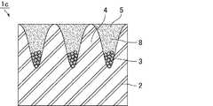
(1)透明導電体の構造
実施形態3の透明導電体の構造について、図5を参照して説明する。図5は、実施形態3の透明導電体を示す断面模式図である。図5に示すように、透明導電体1cは、反射防止フィルム2、金属微粒子3、及び、イオン性液体8を備えている。イオン性液体8は、凸部4の間隙5の上部まで充填されている。本明細書中、凸部4の間隙5の上部は、凸部4の間隙5の深さの50%より高く、100%以下の範囲を示す。実施形態3の透明導電体を示す平面模式図は、イオン性液体8が配置されていること以外、図1と同様である。(1) Structure of transparent conductor The structure of the transparent conductor of
イオン性液体8としては特に限定されず、実施形態2と同様のものを用いることができる。実施形態3の透明導電体においては、イオン性液体8の充填量が多いため、重力等の作用によって、イオン性液体8が流れ出す可能性がある。イオン性液体8が流れ出ることを防止するためには、凸部4やイオン性液体8の材料の組み合わせにより異なるが、凸部4のピッチPを100nm以下に設定することが好ましい。It does not specifically limit as the
実施形態3の透明導電体によれば、実施形態1の透明導電体と同様の効果を奏することができることは明らかである。また、実施形態3の透明導電体によれば、金属微粒子3の間にイオン性液体8を含んでいるため、金属微粒子3の間の接触抵抗が小さくなり、導電部全体の抵抗率を低下させることができる。その結果、透明導電体の導電性をより高めることができる。また、イオン性液体8は透明な物質であるため、その充填量を増加させても、透明導電体の透明性(透過率)の低下を最小限に抑制することができる。更に、イオン性液体8が親水性の材料である場合は、疎水性の汚れに対する防汚性に優れた透明導電体を実現することができる。また、イオン性液体8が疎水性の材料である場合は、親水性の汚れに対する防汚性に優れた透明導電体を実現することができる。According to the transparent conductor of
(2)透明導電体の製造プロセス
実施形態3の透明導電体の製造プロセスは、図3の(d)で示された実施形態1の透明導電体が完成した後に、イオン性液体8を凸部4の間隙5の上部まで充填したこと以外、実施形態1の透明導電体の製造プロセスと同様である。(2) Production process of transparent conductor The production process of the transparent conductor of
以下に、実施形態3の透明導電体を実際に作製した実施例を示す。The Example which actually produced the transparent conductor of
(実施例4)
実施例4の透明導電体は、反射防止フィルム2の凸部4の間隙5の上部までイオン性液体8が充填されていること以外、実施例1の透明導電体と同様である。また、実施例4の透明導電体の製造プロセスは、実施例1の透明導電体が完成した後に、イオン性液体8を凸部4の間隙5の上部まで充填したこと以外、実施例1の透明導電体の製造プロセスと同様である。イオン性液体8としては、関東化学社製の疎水性のイオン性液体(製品名:N、N−ジエチル−N−メチル−N−(2−メトキシエチル)アンモニウムビス(トリフルオロメタンスルホニル)イミド)を用いた。イオン性液体8は、凸部4の間隙5の深さの100%以下の範囲まで充填された。Example 4
The transparent conductor of Example 4 is the same as the transparent conductor of Example 1 except that the
[実施形態4]
実施形態4は、反射防止フィルムと、金属微粒子とを備える透明導電体に関し、実施形態1との違いは、金属微粒子が金属の薄膜で覆われていることである。実施形態4の透明導電体は、この構成以外、実施形態1の透明導電体と同様であるため、重複する点については説明を省略する。[Embodiment 4]
The fourth embodiment relates to a transparent conductor including an antireflection film and metal fine particles, and the difference from the first embodiment is that the metal fine particles are covered with a metal thin film. Since the transparent conductor of
(1)透明導電体の構造
実施形態4の透明導電体の構造について、図6を参照して説明する。図6は、実施形態4の透明導電体を示す断面模式図である。図6に示すように、透明導電体1dは、反射防止フィルム2、及び、金属微粒子3を備えている。金属微粒子3は、金属薄膜9で覆われており、いわゆる金属メッキが施されている。実施形態4の透明導電体を示す平面模式図は、金属薄膜9が配置されていること以外、図1と同様である。(1) Structure of transparent conductor The structure of the transparent conductor of
金属薄膜(金属メッキ)9は、金属微粒子3よりもイオン化傾向が小さい金属であれば特に限定されない。例えば、金属微粒子3としてアルミニウム、亜鉛、鉄、又は、ニッケルを用いた場合は、金属薄膜9として銀、又は、金を用いることができる。また、例えば、金属微粒子3として銀を用いた場合は、金属薄膜9として金を用いることができる。The metal thin film (metal plating) 9 is not particularly limited as long as it has a lower ionization tendency than the
実施形態4の透明導電体によれば、実施形態1の透明導電体と同様の効果を奏することができることは明らかである。また、実施形態4の透明導電体によれば、金属微粒子3が金属薄膜9で覆われているため、導電性をより高め、金属微粒子3をより効率的に凝集させて固定化することができる。このような構成とすることによって、金属微粒子3として金、銀等の高価な材料を用いなくても、導電性を高めることができ、コストを削減することができる。According to the transparent conductor of
(2)透明導電体の製造プロセス
実施形態4の透明導電体の製造プロセスは、図3の(d)で示された実施形態1の透明導電体が完成した後に、金属微粒子3を、金属微粒子3よりもイオン化傾向が小さい金属の薄膜(金属薄膜9)で覆うこと以外、実施形態1の透明導電体の製造プロセスと同様である。金属微粒子3を金属薄膜9で覆う方法としては特に限定されず、例えば、金属微粒子3を無電解メッキ浴に浸漬し、置換型の化学メッキ方法を用いて、金属微粒子3を金属薄膜9で覆う方法等が挙げられる。置換型の化学メッキ方法によれば、金属微粒子3が溶解する際に放出する電子を、無電解メッキ浴中の金属イオンが受け取ることで、金属に還元して析出し、金属微粒子3の表面を覆うことになる。無電解メッキとしては、材料の選択性が大きく、薄いメッキを施すことが可能な置換型の化学メッキ方法を用いることが好ましい。(2) Production process of transparent conductor The production process of the transparent conductor of
(評価結果)
実施例1〜3の透明導電体について、シート抵抗、透過率、反射率、反射色、及び、モアレの有無の評価結果を表1に示す。なお、比較例1として、上記特許文献8の実施例12に記載の方法で製造した透明導電体についても評価を行った。また、比較例2として、厚みが80μmのポリエチレンテレフタレート(PET)フィルム上に、厚みが120nmのITO膜を全面に成膜した構成についても評価を行った。(Evaluation results)
Table 1 shows the evaluation results of sheet resistance, transmittance, reflectance, reflected color, and the presence or absence of moire for the transparent conductors of Examples 1 to 3. As Comparative Example 1, the transparent conductor manufactured by the method described in Example 12 of
シート抵抗の測定は、三菱化学アナリテック社製の抵抗率計(商品名:ロレスタGP MCP−T610型)を用いて行った。The sheet resistance was measured using a resistivity meter (trade name: Loresta GP MCP-T610 type) manufactured by Mitsubishi Chemical Analytech.
透過率の測定は、トプコンテクノハウス社製の輝度計(商品名:BM−9A)を用いて行った。本明細書中、透過率は、入射する可視光に対する可視光透過率を示す。The transmittance was measured using a luminance meter (trade name: BM-9A) manufactured by Topcon Technohouse. In this specification, the transmittance indicates a visible light transmittance with respect to incident visible light.
反射率の測定は、日本分光社製の分光光度計(商品名:V−560)を用いて行った。本明細書中、反射率は、入射する可視光に対する可視光反射率を示す。The reflectance was measured using a spectrophotometer (trade name: V-560) manufactured by JASCO Corporation. In this specification, the reflectance indicates the visible light reflectance with respect to incident visible light.
反射色の評価方法としては、観察者(3名)に、各例のサンプルで蛍光灯の光を反射させた状態を観察してもらい、どのような色に見えるかを評価してもらった。As an evaluation method of the reflected color, observers (three persons) were asked to observe the state in which the light of the fluorescent lamp was reflected by the sample of each example, and evaluated what kind of color it looks.
モアレの評価方法としては、観察者(3名)に、各例のサンプルをシャープ社製の60型の液晶表示装置(商品名:アクオスLX9 FHD)の前面に配置し、かつ、液晶表示装置に全面が緑色の画面を表示させた状態を観察してもらい、モアレが見えるかどうかを評価してもらった。As a method for evaluating moire, an observer (3 persons) placed samples of each example on the front of a 60-inch liquid crystal display device (trade name: Aquos LX9 FHD) manufactured by Sharp Corporation, and the liquid crystal display device We had you observe the state that the whole surface displayed a green screen, and had you evaluate whether you could see moire.

表1に示すように、実施例1〜3はいずれも、比較例2と同程度か、それ以下のシート抵抗を示した。特に、実施例3は、実施例1、2よりも低いシート抵抗を示し、導電性がより優れていると評価された。As shown in Table 1, each of Examples 1 to 3 exhibited a sheet resistance comparable to or lower than that of Comparative Example 2. In particular, Example 3 showed a lower sheet resistance than Examples 1 and 2, and was evaluated to be more conductive.
表1に示すように、実施例1〜3はいずれも、比較例2よりも高い透過率を示した。特に、実施例1は、実施例2、3よりも高い透過率を示し、透明性がより優れていると評価された。As shown in Table 1, all of Examples 1 to 3 showed higher transmittance than Comparative Example 2. In particular, Example 1 showed higher transmittance than Examples 2 and 3, and was evaluated as having better transparency.
表1に示すように、実施例1〜3はいずれも、比較例1、2よりも低い反射率を示した。特に、実施例2は、実施例1、3よりも低い反射率を示し、低反射性がより優れていると評価された。実施例3については、実施例1、2と比べて反射率が高いが、これは、イオン性液体による影響であると考えられる。As shown in Table 1, each of Examples 1 to 3 showed a lower reflectance than Comparative Examples 1 and 2. In particular, Example 2 showed a lower reflectance than Examples 1 and 3, and was evaluated to be more excellent in low reflectivity. The reflectivity of Example 3 is higher than that of Examples 1 and 2, but this is considered to be the effect of the ionic liquid.
表1に示すように、実施例1〜3はいずれも、反射色に色付きがない(無彩色:ニュートラル)と評価された。また、実施例1〜3はいずれも、モアレが観察されなかった。As shown in Table 1, in Examples 1 to 3, it was evaluated that the reflected color was not colored (achromatic color: neutral). In all of Examples 1 to 3, moire was not observed.
[実施形態5]
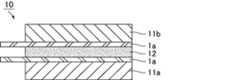
実施形態5は、実施形態1〜4の透明導電体を備えるタッチパネルに関する。以下では、実施形態1の透明導電体を投影型の静電容量方式のタッチパネルに適用する場合について、図7及び図8を参照して説明する。図7は、実施形態5のタッチパネルを示す断面模式図である。図8は、図7中の2つの透明導電体を示す平面模式図である。図7に示すように、タッチパネル10は、対向して配置されたガラス基板11a、11bが接着剤12を介して貼り合わされた構成を有している。ガラス基板11a、11bの接着剤12側の表面には、実施形態1の透明導電体1aが配置されている。ここで、2つの透明導電体1aは、互いの凸部が対向するように配置されている。接着剤12としては、例えば、光学透明粘着シート(OCA:Optical Clear Adhesive)が挙げられる。タッチパネル10は、ガラス基板11bの接着剤12側とは反対側に、接着剤を介してカバーレンズを有していてもよい。このようなタッチパネル10は、液晶表示装置の観察面側に配置されて利用することができる。以下では、ガラス基板11a側に配置された透明導電体1aをX電極とも言い、ガラス基板11b側に配置された透明導電体1aをY電極とも言う。[Embodiment 5]
図8は、図7中のX電極、及び、Y電極に着目した平面模式図である。図8に示すように、X電極は、X方向(横方向)にパターン化されて並んだ導電部を有しており、Y電極は、Y方向(縦方向)にパターン化されて並んだ導電部を有している。このような構成を有するタッチパネル10に対して、例えば、指が触れると、その付近の電極間の静電容量の変化を、X方向の電極列(例えば、X1列、X2列、X3列、X4列)及びY方向の電極列(Y1列、Y2列、Y3列、Y4列)から検知することで、指が触れた位置を判別することができる。ここで、各電極列のパターンは、微視的には、網目状の導電部が一方向(X方向又はY方向)に並んだ形状となっている。このような電極列から構成される、X電極、及び、Y電極を実現する方法としては、例えば、網目状の導電部が間隔を空けて列状に配置された透明導電体を用いる方法、全面に網目状の導電部を有する透明導電体を、間隔を空けて列状に複数並べる方法等が挙げられる。FIG. 8 is a schematic plan view focusing on the X electrode and the Y electrode in FIG. As shown in FIG. 8, the X electrode has a conductive portion patterned and arranged in the X direction (lateral direction), and the Y electrode has a conductive property patterned and arranged in the Y direction (vertical direction). Has a part. For example, when a finger touches the
従来のタッチパネルにおいては、図7中の透明導電体1a(X電極及びY電極)の代わりにITO等の透明電極が用いられ、図8に示したようにパターニングされていた。ITO膜の屈折率は1.9〜2.0程度と高く、接着剤の屈折率(約1.5)と大きく異なるため、これらの界面での反射光が強くなり、ITO膜のパターンが見えてしまうことがあった。これに対して、実施形態5のタッチパネルにおいては、X電極及びY電極の光透過領域(導電部が配置されていない領域)が主に樹脂で形成されており、その領域の屈折率が約1.5となるような材料を選択することができる。よって、X電極及びY電極と接着剤12との界面での不要な反射光が抑制され、導電部のパターンが見えにくくなる。In the conventional touch panel, a transparent electrode such as ITO is used instead of the
以上では、実施形態1の透明導電体をタッチパネルに適用した場合について説明したが、実施形態2〜4の透明導電体をタッチパネルに適用した場合についても同様である。取り扱いの観点からは、実施形態1の透明導電体(乾式)を適用することが好ましい。また、他の方式のタッチパネルに適用されてもよい。Although the case where the transparent conductor of Embodiment 1 is applied to the touch panel has been described above, the same applies to the case where the transparent conductor of
[付記]
以下に、本発明の透明導電体の好ましい態様の例を挙げる。各例は、本発明の要旨を逸脱しない範囲において適宜組み合わされてもよい。[Appendix]
The example of the preferable aspect of the transparent conductor of this invention is given to the following. Each example may be appropriately combined without departing from the scope of the present invention.
上記透明導電体は、更に、上記金属微粒子間にイオン性液体を含むものであってもよい。これにより、上記金属微粒子間の接触抵抗が小さくなり、上記導電部全体の抵抗率を低下させることができる。その結果、上記透明導電体の導電性をより高めることができる。更に、上記イオン性液体が上記複数の凸部の間隙の底部まで入り込む効果によって、上記イオン性液体の表面で汚れを拡散することができる。上記イオン性液体は、親水性の材料であってもよい。また、上記イオン性液体は、疎水性の材料であってもよい。The transparent conductor may further contain an ionic liquid between the metal fine particles. Thereby, the contact resistance between the said metal microparticles becomes small, and the resistivity of the said whole electroconductive part can be reduced. As a result, the conductivity of the transparent conductor can be further increased. Furthermore, dirt can be diffused on the surface of the ionic liquid due to the effect of the ionic liquid entering the bottom of the gap between the plurality of convex portions. The ionic liquid may be a hydrophilic material. The ionic liquid may be a hydrophobic material.
上記イオン性液体は、上記複数の凸部の間隙の上部まで充填されているものであってもよい。上記イオン性液体は、親水性の材料であってもよい。これにより、上記透明導電体の導電性をより高めるとともに、疎水性の汚れに対する防汚性を優れたものとすることができる。また、上記イオン性液体は、疎水性の材料であってもよい。これにより、上記透明導電体の導電性をより高めるとともに、親水性の汚れに対する防汚性を優れたものとすることができる。The ionic liquid may be filled up to the top of the gap between the plurality of convex portions. The ionic liquid may be a hydrophilic material. Thereby, while improving the electroconductivity of the said transparent conductor, it can be made excellent in the antifouling property with respect to hydrophobic dirt. The ionic liquid may be a hydrophobic material. Thereby, while improving the electroconductivity of the said transparent conductor, it can be made excellent in the antifouling property with respect to a hydrophilic stain | pollution | contamination.
上記複数の凸部の上記ピッチは、100nm以下であってもよい。これにより、上記イオン性液体の充填量が多い場合であっても、上記イオン性液体が上記複数の凸部の間隙から流れ出ることを効果的に防止することができる。The pitch of the plurality of convex portions may be 100 nm or less. Thereby, even when the filling amount of the ionic liquid is large, the ionic liquid can be effectively prevented from flowing out from the gaps between the plurality of convex portions.
上記金属微粒子は、上記金属微粒子よりもイオン化傾向が小さい金属の薄膜で覆われているものであってもよい。これにより、上記透明導電体の導電性をより高め、上記金属微粒子をより効率的に凝集させて固定化することができる。更に、上記金属微粒子として金、銀等の高価な材料を用いなくても、上記透明導電体の導電性を高めることができ、コストを削減することができる。The metal fine particles may be covered with a metal thin film having a smaller ionization tendency than the metal fine particles. Thereby, the electroconductivity of the said transparent conductor can be improved more and the said metal fine particle can be more efficiently aggregated and fixed. Further, even if an expensive material such as gold or silver is not used as the metal fine particles, the conductivity of the transparent conductor can be increased and the cost can be reduced.
上記金属微粒子の上記粒径は、50nm以下であってもよい。これにより、上記金属微粒子が、上記複数の凸部の間隙の底部に効率よく充填される。The metal fine particles may have a particle size of 50 nm or less. Thereby, the metal fine particles are efficiently filled into the bottoms of the gaps between the plurality of convex portions.
上記複数の凸部のアスペクト比は、0.8以上、1.5以下であってもよい。これにより、モアレ等の光学現象を充分に防止し、良好な反射率特性を実現することができる。The aspect ratio of the plurality of convex portions may be 0.8 or more and 1.5 or less. As a result, optical phenomena such as moire can be sufficiently prevented, and good reflectance characteristics can be realized.
以下に、本発明の透明導電体の製造方法の好ましい態様の例を挙げる。各例は、本発明の要旨を逸脱しない範囲において適宜組み合わされてもよい。The example of the preferable aspect of the manufacturing method of the transparent conductor of this invention is given to the following. Each example may be appropriately combined without departing from the scope of the present invention.
上記透明導電体の製造方法は、上記工程(3)の前に、上記工程(1)、及び、上記工程(2)を交互に複数回繰り返すものであってもよい。これにより、上記金属微粒子の充填量を効率よく増やすことができるため、上記透明導電体の導電性をより高めることができる。The method for producing the transparent conductor may be such that the step (1) and the step (2) are alternately repeated a plurality of times before the step (3). Thereby, since the filling amount of the metal fine particles can be increased efficiently, the conductivity of the transparent conductor can be further increased.
上記透明導電体の製造方法は、更に、上記工程(3)の後に、上記金属微粒子を、上記金属微粒子よりもイオン化傾向が小さい金属の薄膜で覆う工程(4)を含むものであってもよい。これにより、上記透明導電体の導電性をより高め、上記金属微粒子をより効率的に凝集させて固定化することができる。更に、上記金属微粒子として金、銀等の高価な材料を用いなくても、上記透明導電体の導電性を高めることができ、コストが削減された効率的な上記透明導電体の製造を行うことができる。The method for producing the transparent conductor may further include a step (4) of covering the metal fine particles with a metal thin film having a smaller ionization tendency than the metal fine particles after the step (3). . Thereby, the electroconductivity of the said transparent conductor can be improved more and the said metal fine particle can be more efficiently aggregated and fixed. Furthermore, without using an expensive material such as gold or silver as the metal fine particles, the conductivity of the transparent conductor can be increased, and the transparent conductor can be efficiently manufactured with reduced costs. Can do.
1a、1b、1c、1d:透明導電体
2:反射防止フィルム
3:金属微粒子
4:凸部
5:凸部の間隙
6:溶媒
7:分散液
8:イオン性液体
9:金属薄膜(金属メッキ)
10:タッチパネル
11a、11b:ガラス基板
12:接着剤
13:枝突起
P:ピッチ
DESCRIPTION OF
10:
Claims (11)
Translated fromJapanese前記複数の凸部の前記ピッチ以下の粒径を有し、かつ、前記複数の凸部の間隙の底部に充填された金属微粒子とを備え、
前記複数の凸部の間隙に配置された前記金属微粒子は、網目状の導電部を構成することを特徴とする透明導電体。An antireflection film provided on the surface with a plurality of convex portions at a pitch below the wavelength of visible light, and
A metal fine particle having a particle size equal to or less than the pitch of the plurality of convex portions and filled in a bottom portion of a gap between the plurality of convex portions,
The transparent conductive material, wherein the metal fine particles arranged in the gaps between the plurality of convex portions constitute a network-like conductive portion.
溶媒中に前記金属微粒子が分散された分散液を、前記反射防止フィルム上に塗布する工程(1)、
塗布された前記分散液に対して前記溶媒を蒸発させる乾燥を行う工程(2)、及び、
乾燥された前記分散液に対して加熱を行う工程(3)
を含むことを特徴とする透明導電体の製造方法。A method for producing a transparent conductor according to any one of claims 1 to 8,
Applying the dispersion liquid in which the metal fine particles are dispersed in a solvent on the antireflection film (1),
A step (2) of drying the applied dispersion to evaporate the solvent; and
Heating the dried dispersion (3)
The manufacturing method of the transparent conductor characterized by including.
A touch panel comprising the transparent conductor according to claim 1.
Applications Claiming Priority (3)
| Application Number | Priority Date | Filing Date | Title |
|---|---|---|---|
| JP2014206551 | 2014-10-07 | ||
| JP2014206551 | 2014-10-07 | ||
| PCT/JP2015/077645WO2016056434A1 (en) | 2014-10-07 | 2015-09-30 | Transparent conductor, transparent-conductor production method, and touch panel |
Publications (1)
| Publication Number | Publication Date |
|---|---|
| JPWO2016056434A1true JPWO2016056434A1 (en) | 2017-08-17 |
Family
ID=55653049
Family Applications (1)
| Application Number | Title | Priority Date | Filing Date |
|---|---|---|---|
| JP2016553056APendingJPWO2016056434A1 (en) | 2014-10-07 | 2015-09-30 | Transparent conductor, method for producing transparent conductor, and touch panel |
Country Status (3)
| Country | Link |
|---|---|
| US (1) | US10224126B2 (en) |
| JP (1) | JPWO2016056434A1 (en) |
| WO (1) | WO2016056434A1 (en) |
Cited By (2)
| Publication number | Priority date | Publication date | Assignee | Title |
|---|---|---|---|---|
| CN107977013A (en)* | 2016-10-21 | 2018-05-01 | 三星电子株式会社 | Unmanned vehicle |
| JP2020149014A (en)* | 2019-03-15 | 2020-09-17 | シャープ株式会社 | Super water repellent film |
Families Citing this family (10)
| Publication number | Priority date | Publication date | Assignee | Title |
|---|---|---|---|---|
| US11207478B2 (en) | 2016-03-25 | 2021-12-28 | Rai Strategic Holdings, Inc. | Aerosol production assembly including surface with micro-pattern |
| CN109844572A (en)* | 2016-09-13 | 2019-06-04 | 皇家飞利浦有限公司 | Laminate comprising a wear resistant layer, apparatus comprising said laminate and method of manufacturing said laminate |
| WO2018116136A1 (en)* | 2016-12-20 | 2018-06-28 | 3M Innovative Properties Company | Electrode pattern for capacitive touch sensor |
| CN106814953B (en)* | 2016-12-30 | 2020-05-05 | 青岛海信移动通信技术股份有限公司 | Mobile terminal |
| JP6832527B2 (en)* | 2017-03-17 | 2021-02-24 | パナソニックIpマネジメント株式会社 | Film structure |
| US11297876B2 (en)* | 2017-05-17 | 2022-04-12 | Rai Strategic Holdings, Inc. | Aerosol delivery device |
| CN107678588B (en)* | 2017-09-27 | 2021-01-26 | 京东方科技集团股份有限公司 | Touch screen and touch display device |
| WO2022087727A1 (en)* | 2020-10-26 | 2022-05-05 | Edgehog Advanced Technologies Inc. | Anti-reflection with interconnected structures |
| CN113031356B (en)* | 2021-02-26 | 2023-01-24 | Tcl华星光电技术有限公司 | Display panel and preparation method thereof |
| JP2023148222A (en)* | 2022-03-30 | 2023-10-13 | キヤノン株式会社 | Member |
Citations (7)
| Publication number | Priority date | Publication date | Assignee | Title |
|---|---|---|---|---|
| JP2004259640A (en)* | 2003-02-27 | 2004-09-16 | Tatsuta Electric Wire & Cable Co Ltd | Method of manufacturing anisotropic conductive film connector, anisotropic conductive film connector, and touch panel input device using the same |
| JP2008041445A (en)* | 2006-08-07 | 2008-02-21 | Asahi Glass Co Ltd | Method for producing transparent conductive film and transparent conductive film |
| JP2011526844A (en)* | 2008-06-30 | 2011-10-20 | スリーエム イノベイティブ プロパティズ カンパニー | Method for forming a microstructure |
| WO2013129092A1 (en)* | 2012-03-02 | 2013-09-06 | 東海ゴム工業株式会社 | Hybrid sensor |
| JP2013178550A (en)* | 2013-04-23 | 2013-09-09 | Oji Holdings Corp | Metal thin line sheet having rugged shape |
| JP2013211108A (en)* | 2012-03-30 | 2013-10-10 | Toppan Printing Co Ltd | Conductive complex |
| JP2014092584A (en)* | 2012-10-31 | 2014-05-19 | Dainippon Printing Co Ltd | Transparent conductive film with anti-reflective properties, touch panel, and image display device |
Family Cites Families (20)
| Publication number | Priority date | Publication date | Assignee | Title |
|---|---|---|---|---|
| JPH088080B2 (en) | 1986-12-24 | 1996-01-29 | 株式会社東芝 | Cathode ray tube and method of manufacturing cathode ray tube |
| JP3288557B2 (en) | 1995-08-11 | 2002-06-04 | 住友大阪セメント株式会社 | Cathode ray tube with transparent electromagnetic wave shielding film |
| JPH1126980A (en) | 1997-07-04 | 1999-01-29 | Dainippon Printing Co Ltd | Electromagnetic wave shielding plate and manufacturing method thereof |
| JP2003046293A (en) | 2001-08-02 | 2003-02-14 | Hitachi Chem Co Ltd | Method for producing electromagnetic wave shielding material, magnetic wave shielding material obtained by the method, electromagnetic wave shielding structure and electromagnetic wave shielding display using the same |
| JP3895229B2 (en) | 2002-08-05 | 2007-03-22 | 住友大阪セメント株式会社 | Method for producing transparent conductive film and transparent conductive film produced by this method |
| JP4332610B2 (en) | 2003-07-15 | 2009-09-16 | 三菱マテリアル株式会社 | Composition containing metal nanorod and metal oxide powder and use thereof |
| CN101411255A (en)* | 2006-04-05 | 2009-04-15 | 东丽株式会社 | Conductive substrate and manufacturing method thereof |
| JP2007322767A (en) | 2006-06-01 | 2007-12-13 | Nissan Motor Co Ltd | Anti-reflection structure, anti-reflection structure and manufacturing method thereof |
| JP5082357B2 (en) | 2006-09-22 | 2012-11-28 | 東レ株式会社 | Manufacturing method of reticulated metal fine particle laminated substrate |
| JP2008122435A (en) | 2006-11-08 | 2008-05-29 | Nissan Motor Co Ltd | Water-repellent antireflection structure and manufacturing method thereof |
| JP2008218860A (en) | 2007-03-07 | 2008-09-18 | Toray Ind Inc | Method for manufacturing mesh-like metal particle multi-layer substrate and transparent conductive substrate |
| JP2008283100A (en) | 2007-05-14 | 2008-11-20 | Toray Ind Inc | Methods of manufacturing mesh-like micro-particle-metal laminated substrate and transparent electrically conductive substrate |
| JP5332186B2 (en) | 2007-11-26 | 2013-11-06 | コニカミノルタ株式会社 | Method for producing transparent conductive film using metal nanowire and transparent conductive film produced using the same |
| JP2009224078A (en) | 2008-03-14 | 2009-10-01 | Kyoto Univ | Transparent conductive film and its manufacturing method |
| JP2009263700A (en) | 2008-04-23 | 2009-11-12 | Bridgestone Corp | Electroless plating preprocessing agent, manufacturing method of light-transmissive electromagnetic wave shielding material, and light-transmissive electromagnetic wave shielding material |
| JP2010093239A (en) | 2008-09-09 | 2010-04-22 | Toray Ind Inc | Method for manufacturing board with metal particle laminated thereon like mesh and transparent conductive board |
| JP2010093040A (en) | 2008-10-08 | 2010-04-22 | Bridgestone Corp | Light permeable electromagnetic shield material and method for manufacturing it |
| JP5469849B2 (en) | 2008-10-31 | 2014-04-16 | 富士フイルム株式会社 | Conductive film for touch panel, photosensitive material for forming conductive film, conductive material, and conductive film |
| JP4626721B1 (en) | 2009-09-02 | 2011-02-09 | ソニー株式会社 | Transparent conductive electrode, touch panel, information input device, and display device |
| TWI467214B (en) | 2009-09-02 | 2015-01-01 | Dexerials Corp | A conductive optical element, a touch panel, an information input device, a display device, a solar cell, and a conductive optical element |
- 2015
- 2015-09-30JPJP2016553056Apatent/JPWO2016056434A1/enactivePending
- 2015-09-30USUS15/516,137patent/US10224126B2/enactiveActive
- 2015-09-30WOPCT/JP2015/077645patent/WO2016056434A1/enactiveApplication Filing
Patent Citations (7)
| Publication number | Priority date | Publication date | Assignee | Title |
|---|---|---|---|---|
| JP2004259640A (en)* | 2003-02-27 | 2004-09-16 | Tatsuta Electric Wire & Cable Co Ltd | Method of manufacturing anisotropic conductive film connector, anisotropic conductive film connector, and touch panel input device using the same |
| JP2008041445A (en)* | 2006-08-07 | 2008-02-21 | Asahi Glass Co Ltd | Method for producing transparent conductive film and transparent conductive film |
| JP2011526844A (en)* | 2008-06-30 | 2011-10-20 | スリーエム イノベイティブ プロパティズ カンパニー | Method for forming a microstructure |
| WO2013129092A1 (en)* | 2012-03-02 | 2013-09-06 | 東海ゴム工業株式会社 | Hybrid sensor |
| JP2013211108A (en)* | 2012-03-30 | 2013-10-10 | Toppan Printing Co Ltd | Conductive complex |
| JP2014092584A (en)* | 2012-10-31 | 2014-05-19 | Dainippon Printing Co Ltd | Transparent conductive film with anti-reflective properties, touch panel, and image display device |
| JP2013178550A (en)* | 2013-04-23 | 2013-09-09 | Oji Holdings Corp | Metal thin line sheet having rugged shape |
Cited By (3)
| Publication number | Priority date | Publication date | Assignee | Title |
|---|---|---|---|---|
| CN107977013A (en)* | 2016-10-21 | 2018-05-01 | 三星电子株式会社 | Unmanned vehicle |
| CN107977013B (en)* | 2016-10-21 | 2022-06-03 | 三星电子株式会社 | Unmanned aerial vehicle |
| JP2020149014A (en)* | 2019-03-15 | 2020-09-17 | シャープ株式会社 | Super water repellent film |
Also Published As
| Publication number | Publication date |
|---|---|
| US20170309364A1 (en) | 2017-10-26 |
| US10224126B2 (en) | 2019-03-05 |
| WO2016056434A1 (en) | 2016-04-14 |
Similar Documents
| Publication | Publication Date | Title |
|---|---|---|
| WO2016056434A1 (en) | Transparent conductor, transparent-conductor production method, and touch panel | |
| JP6073683B2 (en) | Glass substrate coated with high refractive index layer under electrode coating and organic light emitting device comprising the substrate | |
| Schneider et al. | Electrohydrodynamic nanodrip printing of high aspect ratio metal grid transparent electrodes | |
| JP5977260B2 (en) | Patterned substrate with dark multilayer conductor traces | |
| CN104090673B (en) | Touch screen sensor with low visibility conductor | |
| TWI479382B (en) | Conducting substrate comprising conducting pattern and touch panel comprising the same | |
| WO2013051548A1 (en) | Conductive sheet, touch panel, display device, and method and program for producing conductive sheet | |
| WO2013051527A1 (en) | Conductive sheet, touch panel, and display device | |
| KR20140002044A (en) | Patterned transparent conductive film based on random grid | |
| KR20230038505A (en) | Display article having diffractive, anti-glare surface and manufacturing method thereof | |
| US20160009928A1 (en) | Composition, substrates and methods thereof | |
| TWI479386B (en) | Conductive substrate and electronic device therewith | |
| JP6843215B2 (en) | Transparent conductors and the process of manufacturing transparent conductors | |
| KR101990841B1 (en) | Pattern formation method | |
| KR20140141469A (en) | Touch-screen conductive film and manufacturing method thereof | |
| US20140283698A1 (en) | Embossing stamp for optically diffuse micro-channel | |
| KR101550481B1 (en) | Touch panel having a improved visibility, method for manufacturing the same and display device comprising the same | |
| TWI587200B (en) | Optically transparent conductive material | |
| WO2016056436A1 (en) | Transparent film, and transparent-film production method | |
| TW201628022A (en) | A light-transparent and conductive material | |
| JP2013054619A (en) | Conductive sheet, touch panel, and display device | |
| JP6175545B2 (en) | Conductive sheet, touch panel, display device | |
| US9865223B2 (en) | Optoelectronic modulation stack | |
| CN104637573A (en) | Conductive film structure | |
| TWM553870U (en) | Conductive film substrate, touch screen sensor and module |
Legal Events
| Date | Code | Title | Description |
|---|---|---|---|
| A621 | Written request for application examination | Free format text:JAPANESE INTERMEDIATE CODE: A621 Effective date:20170403 | |
| A131 | Notification of reasons for refusal | Free format text:JAPANESE INTERMEDIATE CODE: A131 Effective date:20180227 | |
| A521 | Request for written amendment filed | Free format text:JAPANESE INTERMEDIATE CODE: A523 Effective date:20180418 | |
| A02 | Decision of refusal | Free format text:JAPANESE INTERMEDIATE CODE: A02 Effective date:20180703 |