JPWO2016039419A1 - Method for forming surface structure of zirconia ceramics and zirconia ceramics - Google Patents
Method for forming surface structure of zirconia ceramics and zirconia ceramicsDownload PDFInfo
- Publication number
- JPWO2016039419A1 JPWO2016039419A1JP2016547502AJP2016547502AJPWO2016039419A1JP WO2016039419 A1JPWO2016039419 A1JP WO2016039419A1JP 2016547502 AJP2016547502 AJP 2016547502AJP 2016547502 AJP2016547502 AJP 2016547502AJP WO2016039419 A1JPWO2016039419 A1JP WO2016039419A1
- Authority
- JP
- Japan
- Prior art keywords
- periodic structure
- zirconia
- laser
- laser beam
- laser light
- Prior art date
- Legal status (The legal status is an assumption and is not a legal conclusion. Google has not performed a legal analysis and makes no representation as to the accuracy of the status listed.)
- Granted
Links
Images


Classifications
- A—HUMAN NECESSITIES
- A61—MEDICAL OR VETERINARY SCIENCE; HYGIENE
- A61C—DENTISTRY; APPARATUS OR METHODS FOR ORAL OR DENTAL HYGIENE
- A61C8/00—Means to be fixed to the jaw-bone for consolidating natural teeth or for fixing dental prostheses thereon; Dental implants; Implanting tools
- A61C8/0012—Means to be fixed to the jaw-bone for consolidating natural teeth or for fixing dental prostheses thereon; Dental implants; Implanting tools characterised by the material or composition, e.g. ceramics, surface layer, metal alloy
- C—CHEMISTRY; METALLURGY
- C04—CEMENTS; CONCRETE; ARTIFICIAL STONE; CERAMICS; REFRACTORIES
- C04B—LIME, MAGNESIA; SLAG; CEMENTS; COMPOSITIONS THEREOF, e.g. MORTARS, CONCRETE OR LIKE BUILDING MATERIALS; ARTIFICIAL STONE; CERAMICS; REFRACTORIES; TREATMENT OF NATURAL STONE
- C04B35/00—Shaped ceramic products characterised by their composition; Ceramics compositions; Processing powders of inorganic compounds preparatory to the manufacturing of ceramic products
- C04B35/01—Shaped ceramic products characterised by their composition; Ceramics compositions; Processing powders of inorganic compounds preparatory to the manufacturing of ceramic products based on oxide ceramics
- C04B35/48—Shaped ceramic products characterised by their composition; Ceramics compositions; Processing powders of inorganic compounds preparatory to the manufacturing of ceramic products based on oxide ceramics based on zirconium or hafnium oxides, zirconates, zircon or hafnates
- A—HUMAN NECESSITIES
- A61—MEDICAL OR VETERINARY SCIENCE; HYGIENE
- A61C—DENTISTRY; APPARATUS OR METHODS FOR ORAL OR DENTAL HYGIENE
- A61C13/00—Dental prostheses; Making same
- A61C13/0003—Making bridge-work, inlays, implants or the like
- A61C13/0006—Production methods
- A61C13/0018—Production methods using laser
- A—HUMAN NECESSITIES
- A61—MEDICAL OR VETERINARY SCIENCE; HYGIENE
- A61C—DENTISTRY; APPARATUS OR METHODS FOR ORAL OR DENTAL HYGIENE
- A61C8/00—Means to be fixed to the jaw-bone for consolidating natural teeth or for fixing dental prostheses thereon; Dental implants; Implanting tools
- A—HUMAN NECESSITIES
- A61—MEDICAL OR VETERINARY SCIENCE; HYGIENE
- A61F—FILTERS IMPLANTABLE INTO BLOOD VESSELS; PROSTHESES; DEVICES PROVIDING PATENCY TO, OR PREVENTING COLLAPSING OF, TUBULAR STRUCTURES OF THE BODY, e.g. STENTS; ORTHOPAEDIC, NURSING OR CONTRACEPTIVE DEVICES; FOMENTATION; TREATMENT OR PROTECTION OF EYES OR EARS; BANDAGES, DRESSINGS OR ABSORBENT PADS; FIRST-AID KITS
- A61F2/00—Filters implantable into blood vessels; Prostheses, i.e. artificial substitutes or replacements for parts of the body; Appliances for connecting them with the body; Devices providing patency to, or preventing collapsing of, tubular structures of the body, e.g. stents
- A61F2/02—Prostheses implantable into the body
- A61F2/30—Joints
- B—PERFORMING OPERATIONS; TRANSPORTING
- B23—MACHINE TOOLS; METAL-WORKING NOT OTHERWISE PROVIDED FOR
- B23K—SOLDERING OR UNSOLDERING; WELDING; CLADDING OR PLATING BY SOLDERING OR WELDING; CUTTING BY APPLYING HEAT LOCALLY, e.g. FLAME CUTTING; WORKING BY LASER BEAM
- B23K26/00—Working by laser beam, e.g. welding, cutting or boring
- B23K26/352—Working by laser beam, e.g. welding, cutting or boring for surface treatment
- C—CHEMISTRY; METALLURGY
- C04—CEMENTS; CONCRETE; ARTIFICIAL STONE; CERAMICS; REFRACTORIES
- C04B—LIME, MAGNESIA; SLAG; CEMENTS; COMPOSITIONS THEREOF, e.g. MORTARS, CONCRETE OR LIKE BUILDING MATERIALS; ARTIFICIAL STONE; CERAMICS; REFRACTORIES; TREATMENT OF NATURAL STONE
- C04B41/00—After-treatment of mortars, concrete, artificial stone or ceramics; Treatment of natural stone
- C04B41/0036—Laser treatment
- C—CHEMISTRY; METALLURGY
- C04—CEMENTS; CONCRETE; ARTIFICIAL STONE; CERAMICS; REFRACTORIES
- C04B—LIME, MAGNESIA; SLAG; CEMENTS; COMPOSITIONS THEREOF, e.g. MORTARS, CONCRETE OR LIKE BUILDING MATERIALS; ARTIFICIAL STONE; CERAMICS; REFRACTORIES; TREATMENT OF NATURAL STONE
- C04B41/00—After-treatment of mortars, concrete, artificial stone or ceramics; Treatment of natural stone
- C04B41/009—After-treatment of mortars, concrete, artificial stone or ceramics; Treatment of natural stone characterised by the material treated
- C—CHEMISTRY; METALLURGY
- C04—CEMENTS; CONCRETE; ARTIFICIAL STONE; CERAMICS; REFRACTORIES
- C04B—LIME, MAGNESIA; SLAG; CEMENTS; COMPOSITIONS THEREOF, e.g. MORTARS, CONCRETE OR LIKE BUILDING MATERIALS; ARTIFICIAL STONE; CERAMICS; REFRACTORIES; TREATMENT OF NATURAL STONE
- C04B41/00—After-treatment of mortars, concrete, artificial stone or ceramics; Treatment of natural stone
- C04B41/80—After-treatment of mortars, concrete, artificial stone or ceramics; Treatment of natural stone of only ceramics
- C04B41/91—After-treatment of mortars, concrete, artificial stone or ceramics; Treatment of natural stone of only ceramics involving the removal of part of the materials of the treated articles, e.g. etching
- A—HUMAN NECESSITIES
- A61—MEDICAL OR VETERINARY SCIENCE; HYGIENE
- A61C—DENTISTRY; APPARATUS OR METHODS FOR ORAL OR DENTAL HYGIENE
- A61C8/00—Means to be fixed to the jaw-bone for consolidating natural teeth or for fixing dental prostheses thereon; Dental implants; Implanting tools
- A61C8/0018—Means to be fixed to the jaw-bone for consolidating natural teeth or for fixing dental prostheses thereon; Dental implants; Implanting tools characterised by the shape
- A61C8/0037—Details of the shape
- A61C2008/0046—Textured surface, e.g. roughness, microstructure
- C—CHEMISTRY; METALLURGY
- C04—CEMENTS; CONCRETE; ARTIFICIAL STONE; CERAMICS; REFRACTORIES
- C04B—LIME, MAGNESIA; SLAG; CEMENTS; COMPOSITIONS THEREOF, e.g. MORTARS, CONCRETE OR LIKE BUILDING MATERIALS; ARTIFICIAL STONE; CERAMICS; REFRACTORIES; TREATMENT OF NATURAL STONE
- C04B2235/00—Aspects relating to ceramic starting mixtures or sintered ceramic products
- C04B2235/02—Composition of constituents of the starting material or of secondary phases of the final product
- C04B2235/30—Constituents and secondary phases not being of a fibrous nature
- C04B2235/32—Metal oxides, mixed metal oxides, or oxide-forming salts thereof, e.g. carbonates, nitrates, (oxy)hydroxides, chlorides
- C04B2235/3231—Refractory metal oxides, their mixed metal oxides, or oxide-forming salts thereof
- C04B2235/3244—Zirconium oxides, zirconates, hafnium oxides, hafnates, or oxide-forming salts thereof
- C—CHEMISTRY; METALLURGY
- C04—CEMENTS; CONCRETE; ARTIFICIAL STONE; CERAMICS; REFRACTORIES
- C04B—LIME, MAGNESIA; SLAG; CEMENTS; COMPOSITIONS THEREOF, e.g. MORTARS, CONCRETE OR LIKE BUILDING MATERIALS; ARTIFICIAL STONE; CERAMICS; REFRACTORIES; TREATMENT OF NATURAL STONE
- C04B2235/00—Aspects relating to ceramic starting mixtures or sintered ceramic products
- C04B2235/70—Aspects relating to sintered or melt-casted ceramic products
- C04B2235/96—Properties of ceramic products, e.g. mechanical properties such as strength, toughness, wear resistance
- C04B2235/963—Surface properties, e.g. surface roughness
Landscapes
- Health & Medical Sciences (AREA)
- Engineering & Computer Science (AREA)
- Chemical & Material Sciences (AREA)
- Ceramic Engineering (AREA)
- Animal Behavior & Ethology (AREA)
- Oral & Maxillofacial Surgery (AREA)
- Veterinary Medicine (AREA)
- Public Health (AREA)
- General Health & Medical Sciences (AREA)
- Life Sciences & Earth Sciences (AREA)
- Dentistry (AREA)
- Epidemiology (AREA)
- Orthopedic Medicine & Surgery (AREA)
- Materials Engineering (AREA)
- Structural Engineering (AREA)
- Organic Chemistry (AREA)
- Physics & Mathematics (AREA)
- Optics & Photonics (AREA)
- Manufacturing & Machinery (AREA)
- Plasma & Fusion (AREA)
- Mechanical Engineering (AREA)
- Biomedical Technology (AREA)
- Cardiology (AREA)
- Transplantation (AREA)
- Heart & Thoracic Surgery (AREA)
- Vascular Medicine (AREA)
- Composite Materials (AREA)
- Laser Beam Processing (AREA)
- Dental Preparations (AREA)
- Prostheses (AREA)
- Dental Prosthetics (AREA)
Abstract
Translated fromJapaneseDescription
Translated fromJapanese本発明は、ジルコニア系セラミックスの表面に周期的な微細構造を作製する表面構造形成方法及び、表面に周期構造を備えたジルコニア系セラミックスに関する。 The present invention relates to a surface structure forming method for producing a periodic fine structure on the surface of a zirconia ceramic, and a zirconia ceramic having a periodic structure on the surface.
近年、材料表面に微細な凹凸の構造を形成する技術の研究開発が行われている。表面に微細構造を設けることにより、上に形成される膜との固着力、液体の凝着力等を向上させたり、また表面の光学特性を変化させたりすることが可能である。 In recent years, research and development of a technique for forming a fine uneven structure on a material surface has been performed. By providing a fine structure on the surface, it is possible to improve the adhesion with the film formed thereon, the adhesion of liquid, and the like, and to change the optical properties of the surface.
本願が加工対象とするジルコニア系セラミックスは、高強度をもち添加物の濃度や種類により異なる特性を示すことが知られている。イットリア(酸化イットリウム)を所定の濃度ドープした材料は耐靱性をもち、生体材料への応用や機械材料への応用が期待されている。また、素材の持つ性質として酸素イオン伝導性を有することで酸素センサーへの応用なども行われている。 It is known that zirconia ceramics to be processed by the present application have high strength and exhibit different characteristics depending on the concentration and type of additives. A material doped with a predetermined concentration of yttria (yttrium oxide) has toughness and is expected to be applied to biomaterials and mechanical materials. In addition, as a property of the material, it has oxygen ion conductivity, so that it is applied to an oxygen sensor.
ジルコニア系セラミックスは、靱性、硬度、耐摩耗性能などの機械的特性が高いため、機械加工が困難である。難加工材料であるが優れた機械的特性から、ジルコニア系セラミックスの応用として、歯科用のインプラントや代替骨などの生体材料への応用がある。しかし、そのままでは生体との親和性が小さいため、生体親和性を高めるためには表面に生体親和性の高いアパタイトなどの材料をコーティングする技術が望まれる。近年、正方晶ジルコニアを含有する材料は、無毒性であり優れた機械的特性を有することから、医療機器材料として使用が拡大しており、既に、人工関節、歯冠等の歯科修復物、人工歯根に臨床応用されている。しかし、正方晶ジルコニアは、埋入部位の本来の正常組織を材料表面に伝導する組織伝導性がリン酸カルシウムに比較して乏しいことから、骨に埋入する場合も軟組織に埋入する場合も、正方晶ジルコニア表面に薄い(厚さ1−10μm)線維性結合組織が生じて骨や軟組織と直接は結合しない。また、正方晶ジルコニアについては、リン酸カルシウムのような血液適合性が報告されていない。そのため、ジルコニア等のセラミックス材料の表面に組織伝導性のある材料をコーティングすることにより、手術後体内で生体骨と直接結合させる方法が、期待されている。その最適材料として、水酸アパタイト(骨の成分)などのリン酸カルシウムを金属材料やジルコニア等のセラミックス材料の表面にコーティングすることにより骨と結合させることが考えられている。 Zirconia ceramics are difficult to machine because of their high mechanical properties such as toughness, hardness and wear resistance. Although it is a difficult-to-process material, due to its excellent mechanical properties, zirconia ceramics can be applied to biomaterials such as dental implants and alternative bones. However, since the affinity with the living body is small as it is, a technique for coating the surface with a material such as apatite having a high biological affinity is desired in order to increase the biocompatibility. In recent years, tetragonal zirconia-containing materials are non-toxic and have excellent mechanical properties, so that their use as medical device materials has been expanded. Already, dental restorations such as artificial joints and crowns, artificial It is clinically applied to tooth roots. However, since tetragonal zirconia has poor tissue conductivity that conducts the original normal tissue of the implantation site to the material surface compared to calcium phosphate, it is square regardless of whether it is implanted in bone or soft tissue. A thin (thickness 1-10 μm) fibrous connective tissue is formed on the surface of the crystal zirconia and does not directly bond to bone or soft tissue. In addition, tetragonal zirconia has not been reported to have blood compatibility like calcium phosphate. Therefore, a method of directly bonding to a living bone in a body after surgery by coating a surface of a ceramic material such as zirconia with a tissue conductive material is expected. As the optimum material, it is considered that calcium phosphate such as hydroxyapatite (bone component) is coated on the surface of a metal material or a ceramic material such as zirconia to be bonded to bone.
ジルコニアに限らず表面に微細構造を形成することで膜との密着性を高める方法について先行文献調査をしたところ、次のような技術が報告されている。
特許文献1では、ナノレベルの微細加工を行うために、超短パルスレーザー(フェムト秒レーザー)を偏光制御して照射することにより、照射したレーザーの波長より小さいサイズの微細構造を形成する加工法が、報告されている。適切なフルエンスの範囲はアブレーション閾値からアブレーション閾値の10倍であると記載されている。この文献では、「フルエンス」(fluence)とは、レーザー光の1パルス当たりの出力エネルギーを照射断面積で割って求めた単位面積当たりのエネルギー(J/cm2)であると記載され、アブレーション閾値は、レーザーを材料表面に照射することで材料表面が蒸散する現象が生じるエネルギー密度の最小値であると記載されている。特許文献1では、超短パルスレーザーを直線偏光させて固体材料表面に照射することにより、偏光方向とは直交する方向に沿って細長い突起部からなる微細構造を形成でき、また、円偏光させて照射することにより、粒状の突起部からなる微細構造を形成できることが報告されている。微細構造のサイズは、照射するレーザーの波長と正の相関関係があり、波長より著しく小さいサイズ(1/10〜3/5)の微細構造であると報告されている。加工対象として、窒化物セラミックス(TiN)膜、アモルファスカーボン膜及びステンレス鋼の材料を試料として、表面に微細加工を行った例が記載されている。A prior art search was conducted on a method for improving the adhesion to a film by forming a fine structure on the surface, not limited to zirconia, and the following techniques have been reported.
In
特許文献2では、材料表面に一軸のレーザー光を照射して、微細な凹凸を周期的に形成する表面処理方法が報告されている。レーザー光の照射部をオーバーラップさせながら走査して、入射光のp偏光成分と材料表面に沿ったp偏光成分の散乱光の干渉部分のアブレーションによって、自己組織的に入射光の偏光方向に直交した、入射光成分λ/2以上入射光λ以下の間隔を持つ周期構造を作製することが記載されている。同一部分におけるレーザー照射回数が10〜300ショットになるように設定することが記載されている。特許文献2によれば、入射光の偏光方向と直交する方向に周期構造が形成されることを利用して、入射光の偏光方向を変更させることによって、周期構造の方向を変更させることができる、と記載されている。適切なフルエンスの範囲はアブレーション閾値近傍と記載されている。加工対象として、Si基材、Cuテープ、Alテープ表面の試料の例が示されている。
特許文献3では、Siやステンレスの母材表面に周期構造の凹凸を超短パルスレーザーで作製し、水酸アパタイトを蒸着することにより、母材上に骨結合性の高い水酸アパタイト膜を作製する方法が提案されている。 According to
特許文献1乃至3は、いずれも入射光の偏光方向に対して直交する方向に、周期的溝が形成される技術である。また、ジルコニア系セラミックスに対して実験例の報告はない。
フェムト秒レーザー光によるジルコニア系セラミックスの加工について、先行技術調査をしたところ、アブレーション加工による歯科用インプラントジルコニアの数十マイクロメートルの直接的な加工と表面状態の評価に関して、結晶相への影響が小さいことが報告されている程度であり(非特許文献1)、サブミクロンサイズの周期構造等の報告例はない。 A prior art study on the processing of zirconia-based ceramics by femtosecond laser light showed that the effect on the crystal phase was small with regard to the direct processing of dental implant zirconia of several tens of micrometers by ablation and the evaluation of the surface condition. (Non-patent Document 1), there are no reports of submicron-sized periodic structures.
入射光の偏光方向と微細構造の関係について、先行文献調査をしたところ、SiO2材料において入射光の偏光方向に平行な周期的な溝が形成されたことが報告されている(非特許文献2参照)。As a result of prior literature investigation on the relationship between the polarization direction of incident light and the fine structure, it was reported that periodic grooves parallel to the polarization direction of incident light were formed in the SiO2 material (Non-patent Document 2). reference).
従来、母材表面の上の膜の密着性向上の手段として、母材の表面に微細な構造を作成する研究開発が進められている。ジルコニア系セラミックスに対して微細な構造を形成する手段として、機械的な加工やサンドブラストのような物質を介した加工や化学的な反応を利用したエッチング等が考えられるが、素材表面に与える熱的な悪影響や不純物のドーピングの影響などが懸念され、また形成される構造にサブミクロンの周期構造を持たせることは容易ではない。このような悪影響を与えずに、ジルコニア系セラミックスの表面に、サブミクロンサイズの周期の微細構造を実現することが望まれる。 Conventionally, as a means for improving the adhesion of a film on the surface of a base material, research and development for creating a fine structure on the surface of the base material has been advanced. As a means to form a fine structure for zirconia ceramics, mechanical processing, processing through materials such as sandblasting, etching using chemical reaction, etc. can be considered, but the thermal effect given to the material surface There are concerns about such adverse effects and the effects of impurity doping, and it is not easy to give the formed structure a submicron periodic structure. It is desired to realize a submicron-sized fine structure on the surface of zirconia ceramics without causing such an adverse effect.
従来、金属表面に微細構造を形成する方法として、レーザー照射による干渉による光強度の増大を利用したエッチングの例や、表面からの散乱波と入射波の干渉による波長より小さな周期構造の形成例の報告がある(特許文献1乃至3参照)。特許文献2や3の手法は、金属表面やシリコン表面にアブレーションやダメージが生じるフルエンスでレーザー光を照射した際に、固体表面に波長から波長の半分程度の(入射角や屈折率に依存して)凹凸が形成されることに基づくものである。また、材料や照射条件によって波長より著しく小さいサイズ(1/10〜3/5)の微細構造が形成されている。特許文献1乃至の技術は、いずれも入射光の偏光方向に対して直交する方向に、周期的溝が形成される技術である。また、特許文献2では、アブレーション閾値近傍の弱い照射フルエンスから高いフルエンスまで同じ現象が発生するので、空間的なガウス強度分布を有するビームを固体表面に連続的にずらしながら照射して、大きな面積にわたり周期構造が形成されることが示されている。 Conventionally, as a method for forming a fine structure on a metal surface, there are an example of etching utilizing an increase in light intensity due to interference by laser irradiation, and an example of forming a periodic structure smaller than a wavelength due to interference between a scattered wave and incident wave from the surface. There are reports (see
レーザー照射による微細構造の形成方法は、特許文献1乃至3のように、Si、金属、TiN等では報告がなされているが、ジルコニア系セラミックスで周期微細構造形成例はない。 A method for forming a fine structure by laser irradiation has been reported for Si, metal, TiN and the like as in
例えば、特許文献3に示された方法によって、固体表面の凹凸の構造を作製できる可能性はあるとも考えられる。しかし、母材がセラミックス、中でもジルコニアの場合は、加熱による悪影響が問題である。部分安定化ジルコニアでは、加熱により相転移を生じ体積変化が生じてしまう問題がある。体積変化のために、亀裂や破断等の微細構造から甚大な損傷を生じる危険性が高い。したがって、周期構造形成と同時に相転移を生じさせないレーザーの照射条件が重要である。また、従来の文献の技術では、周期構造の凹凸は短パルスレーザーの波長以下で形成されるため、レーザー波長にも依存するが、用いるレーザーの波長がミクロンオーダーであるために多くの構造はサブμmのスケール以下となる。このため、表面加工後の母材上に成膜する工程において、微細構造の周期と同等かこれ以上の固形の微粒子が飛来し付着した際に、凹凸に関係なく接触面積は平坦面より小さくなってしまい、密着性が高い構造とはなりえないという問題もある。 For example, it is considered that there is a possibility that an uneven structure on the solid surface can be produced by the method disclosed in
本発明は、これらの問題を解決しようとするものである。本発明は、ジルコニア系セラミックスの表面に、微細な凹凸の周期構造を形成する表面構造形成方法を提供することを目的とする。本発明は、周期的な凹凸の微細構造を有するジルコニア系セラミックスを提供することを目的とする。周期はサブミクロンからミクロンのサイズ(0.1μm〜10μm程度)が望ましい。 The present invention seeks to solve these problems. An object of this invention is to provide the surface structure formation method which forms the periodic structure of a fine unevenness | corrugation on the surface of a zirconia ceramic. An object of this invention is to provide the zirconia-type ceramics which have a periodic uneven | corrugated microstructure. The period is preferably a submicron to micron size (about 0.1 μm to 10 μm).
本発明は、前記目的を達成するために、以下の特徴を有する。 In order to achieve the above object, the present invention has the following features.
本発明の方法は、ジルコニア系セラミックスの表面構造形成方法であり、ジルコニア系セラミックス表面に、レーザー光を照射して、レーザー光のスポット内に凹凸の周期構造を形成することを特徴とする。
本発明の方法は、ジルコニア系セラミックスの表面構造形成方法であって、直線偏光の超短パルスレーザー光を前記セラミックス表面に照射することにより、前記直線偏光の偏光方向に平行な縞状の凹凸を、レーザー光のスポット内に形成することを特徴とする。
本発明の方法は、ジルコニア系セラミックスの表面構造形成方法であって、円偏光の超短パルスレーザー光を前記セラミックス表面に照射することにより、網目状凸部及び点状凹部を周期的に形成することを特徴とする。
本発明の方法は、ジルコニア系セラミックスの表面構造形成方法において、レーザー光を、周期構造生成部分のみを照射可能な形状の空間制限マスクに集光し、前記形状の像を光学系に転送し、ジルコニア系セラミックス表面に照射して、前記形状の周期構造生成部分を複数個敷き詰めることを特徴とする。The method of the present invention is a method for forming a surface structure of zirconia-based ceramics, and is characterized by irradiating the surface of the zirconia-based ceramics with laser light to form an irregular periodic structure in the laser light spot.
The method of the present invention is a method for forming a surface structure of zirconia ceramics, and by irradiating the ceramic surface with linearly polarized ultrashort pulse laser light, striped irregularities parallel to the polarization direction of the linearly polarized light are formed. The laser beam is formed in a spot of laser light.
The method of the present invention is a method for forming a surface structure of a zirconia ceramic, and periodically forms a mesh-like convex portion and a dot-like concave portion by irradiating the ceramic surface with a circularly polarized ultrashort pulse laser beam. It is characterized by that.
The method of the present invention is a method of forming a surface structure of zirconia-based ceramics, condensing laser light on a space-limiting mask having a shape capable of irradiating only the periodic structure generation portion, and transferring the image of the shape to an optical system. Irradiating the surface of the zirconia-based ceramic, a plurality of periodic structure generation portions having the above-described shape are spread.
本発明のジルコニア系セラミックスは、ジルコニア系セラミックス表面の、レーザー光照射スポット内に凹凸の周期構造が形成されていることを特徴とする。
本発明のジルコニア系セラミックスは、ジルコニア系セラミックス表面の、レーザー光照射スポット内に平行な縞状の凹凸の周期構造が形成されていることを特徴とする。
本発明のジルコニア系セラミックスは、ジルコニア系セラミックス表面の、レーザー光照射スポット内に網目状凸部及び点状凹部の周期構造が形成されていることを特徴とする。The zirconia ceramic of the present invention is characterized in that an irregular periodic structure is formed in a laser light irradiation spot on the surface of the zirconia ceramic.
The zirconia ceramic of the present invention is characterized in that a periodic structure of striped irregularities on the surface of a zirconia ceramic is formed in a laser beam irradiation spot.
The zirconia ceramic of the present invention is characterized in that a periodic structure of mesh-like convex portions and dot-like concave portions is formed in a laser light irradiation spot on the surface of the zirconia ceramic.
本発明により、周期的な、凹凸からなる縞状、又は網目状の凸の微細構造を表面に備えるジルコニア系セラミックスを初めて実現したものである。超短パルスレーザー光の照射により形成するので、凹凸の周期は、用いるレーザーの波長程度の微細構造を形成することができる。 The present invention is the first to realize a zirconia-based ceramic having a periodic, striped or concavo-convex fine structure having irregularities on its surface. Since it is formed by irradiation with ultrashort pulse laser light, it is possible to form a fine structure having a concave / convex period of about the wavelength of the laser used.
本発明の微細構造を表面に有するジルコニア系セラミックスは、超短パルスレーザー光により適切な条件により作製できるので、その表面が熱的な悪影響や不純物のドーピングの影響を受けることがない。 Since the zirconia-based ceramics having the microstructure of the present invention on the surface can be produced by an ultrashort pulse laser beam under appropriate conditions, the surface is not affected by thermal adverse effects or impurity doping.
微細な凹凸の周期構造を実現できたことにより、ジルコニア系セラミックス表面に付着させる膜の密着性が向上し、ジルコニア系セラミックス本来の機械的特性に加えてこれをコーティングした部材全体の、機械的強度や耐熱性を向上させることができる。 By realizing a periodic structure with fine irregularities, the adhesion of the film attached to the surface of the zirconia ceramics is improved, and in addition to the mechanical properties inherent to zirconia ceramics, the mechanical strength of the entire component coated with this And heat resistance can be improved.
レーザー光を連続照射又はスタンプ方式等で照射することにより、微細な凹凸の周期構造を大面積化することができ、周期構造領域の全体に占める面積割合が高いセラミックスを実現できる。 By irradiating the laser beam continuously or by a stamp method, it is possible to increase the area of the periodic structure of fine irregularities, and it is possible to realize a ceramic having a high area ratio in the entire periodic structure region.
本発明の方法により形成された周期微細構造を備えるジルコニア系セラミックは、微細な凹凸によりリン酸カルシウムコーティングの密着性が高められる。 In the zirconia-based ceramic having a periodic microstructure formed by the method of the present invention, the adhesion of the calcium phosphate coating is enhanced by the fine irregularities.
本発明の実施の形態について以下説明する。 Embodiments of the present invention will be described below.
本発明の実施の形態は、表面に、周期的な凹凸からなる縞状、又は周期的な網目状凸部及び点状凹部の微細構造を備えるジルコニア系セラミックスに関する。本発明は、レーザー光をジルコニア系セラミックス部材の表面に照射したところ、レーザー照射スポット内に、凹凸の周期微細構造が形成される、という新規な知見に基づく。より具体的には、直線偏光のレーザー光を照射した場合は、偏光方向に対して平行の方向に凹凸の縞状の周期微細構造が形成され、円偏光のレーザー光を照射した場合は、網目状凸部及び点状凹部の周期微細構造が形成される、という新規な知見に基づく。 Embodiments of the present invention relate to a zirconia-based ceramic provided with a fine structure of stripes or periodic mesh-like convex portions and dot-like concave portions consisting of periodic irregularities on the surface. The present invention is based on the novel finding that when a laser beam is irradiated on the surface of a zirconia ceramic member, an irregular periodic fine structure is formed in the laser irradiation spot. More specifically, when irradiated with linearly polarized laser light, a striped periodic fine structure is formed in a direction parallel to the polarization direction, and when irradiated with circularly polarized laser light, a mesh This is based on a novel finding that a periodic fine structure of a ridge-shaped convex portion and a point-shaped concave portion is formed.
本発明の実施の形態において、レーザー光は、ジルコニア表面の凹凸加工に際しては熱的な影響を与えにくい超短パルスレーザー(フェムト秒レーザー(フェムト秒レベルの間だけ発光することのできるレーザーのこと、なお本発明の実施の形態では、10ps以下のパルス幅を含む。)を用いる。超短パルスレーザーにより照射された部分は形状変化を生じるが、ピークパワーが高いためパルス全体としてのエネルギーは極めて抑えられ、パルスが短いため、吸収した熱が照射表面から内部や表面周囲に拡散することなく照射された部分のみアブレーションで吹き飛ぶ。 In the embodiment of the present invention, the laser beam is an ultrashort pulse laser (a femtosecond laser (a laser that can emit light only during the femtosecond level), which is less likely to be thermally affected during the concavo-convex processing of the zirconia surface. Note that in the embodiment of the present invention, a pulse width of 10 ps or less is used.) The portion irradiated with the ultrashort pulse laser undergoes a shape change, but the energy of the entire pulse is extremely suppressed because of the high peak power. Since the pulse is short, the absorbed heat is blown off by ablation without diffusing the absorbed heat from the irradiated surface to the inside or around the surface.
本発明の実施の形態で用いるレーザー光として、フェムト秒レーザーとして知られるチタンサファイアレーザーやイットリビウム系のレーザー(フェムト秒(fs)レベルに加えて1ps―10psも含む。)を使うことができる。また、非線形波長変換過程に基づくパラメトリック増幅装置による波長可変フェムト秒パルス光源を使うことができる。 As a laser beam used in the embodiment of the present invention, a titanium sapphire laser known as a femtosecond laser or an yttrium laser (including 1 ps-10 ps in addition to the femtosecond (fs) level) can be used. In addition, a tunable femtosecond pulsed light source using a parametric amplifier based on a nonlinear wavelength conversion process can be used.
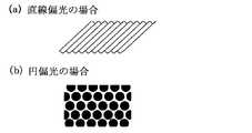
偏光には、直線偏光、円偏光、またはより一般的な表現である楕円偏光がある。本実施の形態では、直線偏光の入射レーザー光を使用した場合は、偏光方向に対して平行の方向に、凹凸の縞状の周期微細構造が形成される。また、本実施の形態では、円偏光の入射レーザー光を使用した場合は、凹凸の縞状周期微細構造は形成されず、網目状凸部及び点状凹部の周期微細構造が形成される。 Polarized light includes linearly polarized light, circularly polarized light, or elliptical polarized light, which is a more general expression. In the present embodiment, when linearly polarized incident laser light is used, a striped periodic fine structure with irregularities is formed in a direction parallel to the polarization direction. Further, in this embodiment, when circularly polarized incident laser light is used, the uneven periodic striped fine structure is not formed, but the periodic fine structure of the mesh-like convex portions and the dotted concave portions is formed.
直線偏光のレーザー光を基材に入射する場合、入射面(反射面に垂直でかつ入射光を含む面をいう)に垂直であるs偏光の場合も、入射面に平行であるp偏光の場合も、いずれも、偏光方向に平行に縞状の周期構造が形成される。 When linearly polarized laser light is incident on a substrate, in the case of s-polarized light that is perpendicular to the incident surface (which means a surface that is perpendicular to the reflecting surface and includes incident light), and p-polarized light that is parallel to the incident surface In both cases, a striped periodic structure is formed parallel to the polarization direction.
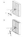
図1は、本発明の概要を説明するための図であり、被加工物に入射するレーザー光の偏光方向と形成される被加工物表面の周期構造とを説明する図である。被加工物に入射するレーザー光の偏光方向がs偏光の場合、ジルコニア系セラミックスの表面の凹凸の周期構造は偏光方向に平行な縞状となる((a)図参照)。被加工物に入射するレーザー光の偏光方向がp偏光の場合、ジルコニア系セラミックスの表面の凹凸の周期構造は偏光方向に平行な縞状となる((b)図参照)。なお、θは入射光の入射角度を示す。 FIG. 1 is a diagram for explaining the outline of the present invention, and is a diagram for explaining the polarization direction of laser light incident on a workpiece and the periodic structure of the workpiece surface to be formed. When the polarization direction of the laser light incident on the workpiece is s-polarized light, the periodic structure of the irregularities on the surface of the zirconia ceramic becomes a stripe shape parallel to the polarization direction (see FIG. 5A). When the polarization direction of the laser light incident on the workpiece is p-polarized light, the periodic structure of the irregularities on the surface of the zirconia ceramic becomes a stripe shape parallel to the polarization direction (see FIG. 5B). Note that θ represents the incident angle of incident light.
図2は、本発明の実施の形態における、レーザー光照射の空間分布(上段)と、レーザー光によりアブレーションされたスポット跡の表面の構造分布(中段)と、穴の深さの分布(下段)の関係を説明する図である。上段の縦軸は、フルエンス(Fluence)である。 FIG. 2 shows the spatial distribution (upper stage) of laser light irradiation, the structure distribution of the surface of the spot trace ablated by the laser light (middle stage), and the distribution of the depth of the hole (lower stage) in the embodiment of the present invention. It is a figure explaining the relationship. The vertical axis in the upper stage is fluence.
フルエンスは、ある場所に照射されたレーザー光の一パルスあたりの単位面積当たりのエネルギーであり、均一なビームの場合にはレーザー光の1パルス当たりの出力エネルギーを照射断面積で割って求めたエネルギー(J/cm2)で与えられる。空間的にガウシアンビームの場合にはパルスエネルギーがE、1/e2強度でのビーム半径をrとすると、ビーム中央での最大値であるピークフルエンスFpeakは次式で与えられる。
Fpeak = 2・E/(πr2)The fluence is the energy per unit area per pulse of the laser light irradiated to a certain location. In the case of a uniform beam, the energy obtained by dividing the output energy per pulse of the laser light by the irradiation cross section (J / cm2 ). In the case of a Gaussian beam spatially, if the pulse energy is E and the beam radius is r with 1 / e2 intensity, the peak fluence Fpeak at the center of the beam is given by the following equation.
Fpeak = 2 · E / (πr2 )
図2の下段の下向き縦軸は、穴の深さの分布(Depth)を示す。あるショット数だけレーザーパルスを照射した後の形状を示している。横軸は、スポットの半径方向の距離を示す。(a)(b)図の、中段の表面の構造分布において、縦縞模様は、凹凸の周期構造が形成されている領域を示し、その外側の点状環状部は、アブレーション跡はあるが周期構造が明確に形成されていない領域を示す。(b)図の中段の表面の構造分布において、円中央部分のまだら模様は、周期構造が崩れている領域を示す。 The downward vertical axis in FIG. 2 indicates the hole depth distribution (Depth). The shape after irradiation with a laser pulse for a certain number of shots is shown. The horizontal axis indicates the radial distance of the spot. (A) In the structure distribution on the surface of the middle stage in FIGS. (A) and (b), the vertical stripe pattern indicates the region where the irregular periodic structure is formed, and the outer dotted dotted portion has the ablation mark but the periodic structure. Indicates a region that is not clearly formed. (B) In the structure distribution of the surface in the middle of the figure, the mottled pattern at the center of the circle indicates a region where the periodic structure is broken.
図中、FLLは、周期構造が形成されるフルエンスの有効範囲の下限値を示す。Fthは、アブレーション跡が形成されるフルエンスのアブレーション閾値を示す。FULは、周期構造が形成されるフルエンスの上限値、DLLは、周期構造が形成される穴の深さの有効範囲の下限値を示す。DULは、周期構造が形成される穴の深さの有効範囲の上限値を示す。In the figure, FLL indicates the lower limit value of the effective range of the fluence in which the periodic structure is formed. Fth indicates the fluence ablation threshold at which an ablation mark is formed. FUL indicates the upper limit value of the fluence at which the periodic structure is formed, and DLL indicates the lower limit value of the effective range of the depth of the hole in which the periodic structure is formed.DUL indicates the upper limit value of the effective range of the depth of the hole in which the periodic structure is formed.
(a)図は、FpeakがFULより小の場合を示す。穴の深さは、Dbottom(穴の底面の深さ)<DULの場合である。(a)図では、穴の深さDが、0<D<DLLの領域は、周期構造が不明瞭で、DLL<D<Dbottomの領域(図の縦縞の部分)には周期構造が形成されていることを、模式的に表している。(A) The figure shows the case where Fpeak is smaller than FUL . The depth of the hole is Dbottom (the depth of the bottom of the hole) <DUL . (A) In the figure, the region where the hole depth D is 0 <D <DLL has an unclear periodic structure, and the region where DLL <D <Dbottom (the vertical stripes in the figure) has a periodic structure. Is schematically formed.
(a)図よりフルエンスが上がると、(b)図のようになる。(b)図は、Fpeak(フルエンスのピーク強度)がFULより大の場合を示す。穴の深さは、穴の底面の深さDbottom>DULである。(b)図のように、フルエンスが上がると、レーザースポットによる穴の中央部分は周期構造が崩れて、周期構造が形成される領域はドーナッツ状(環状)になる。穴の深さDが、0<D<DLLの領域は周期構造が不明瞭で、DLL<D<DULの領域(図中、縦縞の部分)は周期構造が形成されている領域であり、DUL<D<Dbottomの領域は、フルエンスが高すぎて周期構造が崩れた領域である。(A) When the fluence increases from the figure, it becomes as shown in (b). (B) The figure shows the case where Fpeak (peak intensity of fluence) is greater than FUL . The depth of the hole is such that the bottom depth Dbottom > DUL of the hole. (B) As shown in the figure, when the fluence rises, the periodic structure is broken in the center portion of the hole due to the laser spot, and the region where the periodic structure is formed becomes donut-shaped (annular). The region where the hole depth D is 0 <D <DLL has an unclear periodic structure, and the region where DLL <D <DUL (the vertical stripes in the figure) is a region where the periodic structure is formed. In otherwords , the region of DUL <D <Dbottom is a region in which the periodic structure is broken because the fluence is too high.
図2に表示した2つの場合の他に、フルエンスピーク強度が、Fth<Fpeak<FLLの場合、Fpeak<FLLの場合があるが、周期構造形成領域がない場合であり省略する。In addition to the two cases shown in FIG. 2, when the fluence peak intensity is Fth <Fpeak <FLL , there may be a case where Fpeak <FLL , but this is a case where there is no periodic structure formation region and is omitted. .
図3は、直線偏光と円偏光の場合の、周期構造とその周期及び深さの関係等を模式的に説明する図である。(a)図は、入射光が直線偏光の場合を示す。(b)図は、入射光が円偏光の場合を示す。円偏光の場合には黒で表した凹部分が周期的に形成され、凸部分が網目状になる。入射光が直線偏光の場合は、縞の周期は、照射するレーザー波長と同程度(約0.9倍から1.3倍の範囲)である。縞の深さは縞の周期の半分程度よりも小さい。入射光が円偏光の場合は、小さな穴が周期的に並び該穴を囲む凸部分が網目状の構造で、即ち、縞が網目状に変化した形状となっており、直径が波長程度であり、周期が同様に、照射するレーザー波長と同程度(約0.9倍から1.3倍の範囲)である。 FIG. 3 is a diagram schematically illustrating the periodic structure and the relationship between the period and the depth in the case of linearly polarized light and circularly polarized light. (A) The figure shows the case where incident light is linearly polarized light. (B) A figure shows the case where incident light is circularly polarized light. In the case of circularly polarized light, the concave portions represented by black are periodically formed, and the convex portions have a mesh shape. When the incident light is linearly polarized light, the period of the fringes is about the same as the laser wavelength to be irradiated (a range of about 0.9 times to 1.3 times). The fringe depth is smaller than about half of the fringe period. When the incident light is circularly polarized light, the small holes are arranged periodically and the convex part surrounding the holes has a network structure, that is, the stripes are changed into a network shape, and the diameter is about the wavelength. Similarly, the period is about the same as the laser wavelength to be irradiated (in the range of about 0.9 to 1.3 times).
周期凹凸を持つ微細構造を生成するために、同一位置において超短パルスレーザーが数10回ないし数百回照射される様に設定を行う。この回数をショット数という。 In order to generate a fine structure having periodic irregularities, setting is performed so that an ultrashort pulse laser is irradiated several tens to several hundreds of times at the same position. This number is called the number of shots.
レーザー光を被加工物に照射して、微細な周期構造を形成するための条件については後述する実施の形態で詳しく述べるが、レーザー光の種類(波長)、レーザー光のフルエンス、ショット数、エッチレート(単位ショット当たりのエッチング深さ)、パルス幅等を適宜設定することにより、形成目的とする周期構造の状態(周期、形成面積、周期構造部分の割合等)を調整することが可能である。なお、各実施の形態では、入射光が直線偏光の場合について詳細に記載するが、円偏光の場合は、縞(1次元の周期構造)が網目状(二次元の周期構造)に変化した形状となっていることから、その周期構造を調整するためのレーザー光の条件は、直線偏光の場合と同様になる。 The conditions for irradiating a workpiece with laser light to form a fine periodic structure will be described in detail in the embodiments described later. The type (wavelength) of laser light, the fluence of laser light, the number of shots, and etching By appropriately setting the rate (etching depth per unit shot), pulse width, etc., it is possible to adjust the state of the periodic structure to be formed (period, formation area, ratio of periodic structure portion, etc.). . In each embodiment, the case where the incident light is linearly polarized light will be described in detail. However, in the case of circularly polarized light, the shape in which the stripes (one-dimensional periodic structure) are changed to a mesh shape (two-dimensional periodic structure). Therefore, the conditions of the laser beam for adjusting the periodic structure are the same as in the case of linearly polarized light.
レーザー光の種類(波長)は、上述したように、チタンサファイアレーザー(約0.8μm)やイットリビウム系のレーザー(約1μm)が好ましい。その他、非線形光学過程のパラメトリック波長変換を利用した増幅装置や、これらを基本として波長変換を覆なった光源でもよい、波長は特に限定されない。 As described above, the type (wavelength) of the laser light is preferably a titanium sapphire laser (about 0.8 μm) or an yttrium-based laser (about 1 μm). In addition, the wavelength is not particularly limited, and may be an amplifying apparatus using parametric wavelength conversion in a nonlinear optical process or a light source that covers wavelength conversion based on these.
パルス幅は、フェムト秒レベルであれば縞状周期構造が形成されることがわかり、10fsから10ps程度まで可能である。500fs以下であればガウシアンビームでも周期構造が形成される面積の割合を50%以上に高くできる点から好ましい。また、100fs以下であれば、面積の割合を65%よりも大きくでき、より好ましい。 If the pulse width is a femtosecond level, it can be seen that a striped periodic structure is formed, and can be about 10 fs to 10 ps. If it is 500 fs or less, it is preferable because the ratio of the area where the periodic structure is formed can be increased to 50% or more even with a Gaussian beam. Moreover, if it is 100 fs or less, the ratio of an area can be larger than 65%, and it is more preferable.
ショット数は12ショット以上400ショット未満程度であれば周期構造が形成可能である。最適な範囲は20−70ショット程度である。 If the number of shots is about 12 shots or more and less than 400 shots, a periodic structure can be formed. The optimum range is about 20-70 shots.
エッチレートは、[エッチレート/波長]が、0.16−0.34の範囲である場合に、縞状の周期構造が確実に形成できる。 When the etch rate [etch rate / wavelength] is in the range of 0.16-0.34, a striped periodic structure can be reliably formed.
周期構造の形成される面積の割合を増加させるためには、強度分布を均一化したビームを使用することが好ましい。また、照射フルエンスの均一化の方法として、ピンホール等に集光し周期構造形成に寄与しない部分のレーザー光を除去し、このピンホール等を像転送でジルコニア上に照射することで照射面積中の周期構造生成の面積割合を高くできる In order to increase the ratio of the area where the periodic structure is formed, it is preferable to use a beam having a uniform intensity distribution. In addition, as a method of making the irradiation fluence uniform, the laser light that is focused on pinholes and other parts that do not contribute to the formation of the periodic structure is removed, and this pinhole is irradiated onto zirconia by image transfer to reduce the irradiation area. The area ratio of periodic structure generation can be increased
また、ジルコニア系セラミックス表面に形成する周期構造を大面積化するには、同一カ所に所定回数照射して照射部分全体に構造を作成したのち、いくらかの重なりを持つように、又は隣り合う位置、又はそれ以上間隔をあけて、ビームをずらして、同様の照射をして構造を作成することを繰り返すことにより、多数のスポット跡の集合により大面積化をすることができる。 In addition, in order to increase the area of the periodic structure formed on the surface of the zirconia-based ceramics, after creating a structure over the entire irradiated portion by irradiating the same spot a predetermined number of times, there is some overlap, or adjacent positions, Alternatively, it is possible to increase the area by gathering a large number of spot traces by repeating the creation of the structure by shifting the beam and performing the same irradiation with a further interval.
本発明の実施の形態において、ジルコニア系セラミックスとして、ジルコニア系セラミックス基板や板状体に限定されないジルコニア系セラミックス基材等が例示できる。また、ジルコニア系セラミックスには、基材の表面がジルコニア膜やジルコニア系セラミックスで被覆されているものも含まれる。 In the embodiment of the present invention, examples of zirconia ceramics include zirconia ceramic substrates and zirconia ceramic substrates that are not limited to plate-like bodies. Further, the zirconia ceramic includes those in which the surface of the substrate is coated with a zirconia film or a zirconia ceramic.
本発明の実施の形態において、ジルコニア系セラミックスの例として、正方晶ジルコニアが挙げられる。また、正方晶ジルコニアを含有する医療機器材料が挙げられる。正方晶ジルコニアを含有する医療機器材料は、正方晶ジルコニアを含有し、生体内に直接埋植、若しくは非埋植でも生体組織や体液に直接接触して使用する医療機器材料である。ジルコニア系セラミックスには、正方晶ジルコニアの含有率が100%である正方晶ジルコニア多結晶体(TZP)、正方晶ジルコニアと単斜晶ジルコニアから成る部分安定化ジルコニア(PSZ)、正方晶ジルコニアを含む非安定化ジルコニアで母材セラミック(Al2O3、SiC等)を高靱性化したジルコニア高靱性化セラミックス(ZTC)、及び正方晶ジルコニアの表面被覆や分散による金属ジルコニウムやその他金属との複合体等がある。また、正方晶ジルコニアの安定化に使用される安定化剤(CaO、MgO、Y2O3、CeO2等)とその含有量については、正方晶が安定化できれば特に制限はない。In the embodiment of the present invention, tetragonal zirconia is an example of the zirconia ceramic. Moreover, the medical device material containing a tetragonal zirconia is mentioned. The medical device material containing tetragonal zirconia is a medical device material which contains tetragonal zirconia and is used by being directly implanted into a living body or in direct contact with a living tissue or body fluid. Zirconia ceramics include tetragonal zirconia polycrystal (TZP) having a tetragonal zirconia content of 100%, partially stabilized zirconia (PSZ) composed of tetragonal zirconia and monoclinic zirconia, and tetragonal zirconia. Zirconia toughened ceramics (ZTC) made of non-stabilized zirconia with a base ceramic (Al2 O3 , SiC, etc.) toughened, and composites of metal zirconium and other metals by surface coating and dispersion of tetragonal zirconia Etc. Further, the stabilizer (CaO, MgO, Y2 O3 , CeO2 and the like) used for stabilizing tetragonal zirconia and the content thereof are not particularly limited as long as the tetragonal crystal can be stabilized.
本発明の実施の形態のように表面周期構造を備えるジルコニア系セラミックス、例えば正方晶ジルコニアを含有する医療機器材料の特定部位の表面に、形成された凹凸の周期に比べて小さいリン酸カルシウム微粒子の付着層を形成すると、リン酸カルシウムコーティングの密着性を高めることができる。 Adhesion layer of calcium phosphate fine particles that is smaller than the period of irregularities formed on the surface of a specific part of a medical device material containing a surface periodic structure as in the embodiment of the present invention, for example, tetragonal zirconia Can improve the adhesion of the calcium phosphate coating.
(第1の実施の形態)
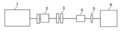
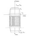
本実施の形態を図4及び5を参照して以下説明する。図4は、本実施の形態において使用するレーザー光による表面加工装置の概略図である。図4の装置は、レーザー発生装置1、パワー制御装置2、偏光状態制御装置3、ビーム整形装置4、集光レンズ5、及び照射用ステージ6を備える。パワー制御装置2は、レーザー光のパワー(単位W)、あるいはレーザー光の一パルスあたりのエネルギー(単位J))を制御する。偏光状態制御装置3は、レーザー光の、偏光方向や直線偏光か楕円偏光か円偏光という偏光状態を制御する。ビーム整形装置4は、ビーム形状とビーム内での強度分布と、ビームの進行方向を制御する。照射用ステージ6は、加工対象物を載置して、レーザー光との相対的位置(x、y、z、θ、φ)を自在に移動可能とする台である。レーザー発生装置1から出射されるレーザー光を、パワー制御装置2、偏光状態制御装置3、ビーム整形装置4、集光レンズ5等を順に介して、照射用ステージ6上の被加工物に照射する。(First embodiment)
This embodiment will be described below with reference to FIGS. FIG. 4 is a schematic view of a surface processing apparatus using laser light used in the present embodiment. The apparatus of FIG. 4 includes a
ジルコニア系セラミックスの表面に、直線偏光のレーザー光(チタンサファイア(「TiS」と略す。)(波長約0.8ミクロン)、パルス幅80fs)を照射すると、表面に、平行な縞状の凹凸からなる微細な周期構造が形成された。レーザー光の直線偏光の偏光方向と縞とは平行であった。周期構造は、周期が平均およそ948nm/cycleであった。照射したレーザー光の波長と同程度で波長より長めの周期構造が観測された。レーザー顕微鏡により観測したところ、形成された構造の深さ(凹凸の谷の底から山の頂上まで)が350−400nmであることがわかった。深さは周期の1/3−1/2程度であった。 When the surface of zirconia ceramics is irradiated with linearly polarized laser light (titanium sapphire (abbreviated as “TiS”) (wavelength: about 0.8 micron), pulse width: 80 fs), the surface is exposed to parallel striped irregularities. A fine periodic structure was formed. The polarization direction of the linearly polarized light of the laser beam and the stripes were parallel. The periodic structure had an average period of about 948 nm / cycle. A periodic structure was observed that was almost the same as the wavelength of the irradiated laser beam and longer than the wavelength. When observed with a laser microscope, it was found that the depth of the formed structure (from the bottom of the uneven valley to the top of the peak) was 350-400 nm. The depth was about 1 / 3-1 / 2 of the period.
図5は、直線偏光のレーザー光を照射した照射跡を示すレーザー顕微鏡写真及び直線偏光の偏光方向を示す矢印である。レーザー照射跡は、直線偏光の偏光方向と平行な縦縞の縞状の凹凸の構造と、周期構造を囲んで縞が不明瞭な環状のアブレーション跡からなることがわかる。図5は図2の中段のアブレーションされた表面の分布模式図の(a)図に対応している。 FIG. 5 is a laser micrograph showing an irradiation trace irradiated with linearly polarized laser light and an arrow indicating the polarization direction of linearly polarized light. It can be seen that the laser irradiation trace is composed of a striped uneven structure of vertical stripes parallel to the polarization direction of linearly polarized light, and an annular ablation trace surrounding the periodic structure with unclear stripes. FIG. 5 corresponds to (a) of the distribution schematic diagram of the ablated surface in the middle of FIG.
ジルコニア系セラミックスの表面に、円偏光のレーザー光(TiS(波長約0.8ミクロン)、パルス幅80fs)を照射すると、レーザー照射跡に、縞ではなく、凸部が網状になった、即ち、縞が網目状に変化した形状となった周期構造が現れ、周期構造を囲んで網目状が不明瞭な環状のアブレーション跡からなることを確認した。 When the surface of the zirconia-based ceramics was irradiated with circularly polarized laser light (TiS (wavelength: about 0.8 micron), pulse width: 80 fs), the laser irradiation traces were not striped, but the projections were reticulated. It was confirmed that a periodic structure in which the stripes changed into a mesh shape appeared, and the periodic structure surrounded the annular structure with an unclear mesh shape.
微細構造を表面に有するジルコニア系セラミックスの表面における、結晶相の加工前後の変化について観測した。ラマン顕微鏡およびX線回折により観測した結果は、結晶相の変化(正方晶から単斜晶への変化)は2%以下であった。このことから、表面が熱的あるいは機械的な悪影響をほとんど受けていないことを確認した。 Changes in the crystal phase before and after processing were observed on the surface of zirconia ceramics with a fine structure. As a result of observation by a Raman microscope and X-ray diffraction, the change of crystal phase (change from tetragonal to monoclinic) was 2% or less. From this, it was confirmed that the surface was hardly affected by thermal or mechanical effects.
直線偏光のレーザー光(TiS(波長約0.8ミクロン)、パルス幅80fs)を連続的に走査、即ちずらしながら照射して、走査を停止(終了)した場合、最終の照射スポット跡には、偏光方向に対して平行な縞状の周期構造が得られた。縞状の方向は走査方向には依存せずに、偏光方向に依存していることを確認した。照射スポット跡の中央部の周期構造を囲む周辺部には、周期構造を示さない環状のアブレーション跡が形成され、走査跡では周期構造が崩れていた。 When a linearly polarized laser beam (TiS (wavelength: about 0.8 micron),
強度分布がガウシアンビームであるレーザー光を連続的にずらしながら照射すると、ジルコニア系セラミックスでは、ある閾値以上のフルエンスで周期構造が形成されるが、当該閾値以下のフルエンスでかつアブレーション閾値以上のフルエンス領域がビーム内に存在するため、低いフルエンス部分が通過することにより、形成された周期構造が破壊されてしまうことを確認した。 When irradiating laser light whose intensity distribution is a Gaussian beam while continuously shifting, in zirconia ceramics, a periodic structure is formed with a fluence above a certain threshold, but a fluence region below the threshold and above the ablation threshold Was present in the beam, it was confirmed that the formed periodic structure would be destroyed by passing a low fluence portion.
(第2の実施の形態)
本実施の形態では、第1の実施の形態とは異なるレーザー光を使用した。
ジルコニア系セラミックスの表面に、直線偏光のレーザー光(Yb系KGW(KGd(WO4)2)(波長1.03ミクロン)、パルス幅200fs)を照射すると、表面に、平行な縞状の凹凸からなる微細な周期構造が形成された。レーザー光は50ショット照射した。レーザー光の直線偏光の偏光方向と縞とは平行であった。周期構造は、周期が平均およそ1.05μm/cycleであった。照射したレーザー光の波長と同程度で波長より長めの周期が観測された。使用するレーザー光が異なっても、第1の実施の形態と同様の表面構造が得られた。(Second Embodiment)
In the present embodiment, a laser beam different from that in the first embodiment is used.
When the surface of zirconia ceramics is irradiated with linearly polarized laser light (Yb-based KGW (KGd (WO4 )2 ) (wavelength 1.03 microns),
(第3の実施の形態)
本実施の形態を、図6、7、8を参照して説明する。本実施の形態では、周期構造を形成することができる最適条件などについて説明する。(Third embodiment)
The present embodiment will be described with reference to FIGS. In the present embodiment, optimum conditions for forming a periodic structure will be described.
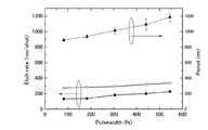
エッチレートとは、レーザー光1ショットあたりのエッチングされた穴の深さDをいい、本実施例においては例えば40ショットで形成された穴の深さをショット数40で割った値として平均値として求めており、単位はnm/shot、である。ここで分母の「shot」は単位ショットあたりの平均的値であることを意味する。 The etch rate refers to the depth D of etched holes per one shot of laser light. In this embodiment, for example, the depth of holes formed by 40 shots is divided by 40 shots as an average value. The unit is nm / shot. Here, “shot” in the denominator means an average value per unit shot.
図6は、直線偏光のレーザー光(TiS(波長810nm)、80fs)の照射を40ショット行った場合の、エッチレートと、表面の縞状の周期構造の有無などの表面状態との関係を示す図である。図の横軸はエッチレート(単位nm/shot)、縦軸は、レーザースポット跡の状態を「跡なし」「(跡があるが)周期構造なし」「周期構造形成」「周期構造崩れ」の4段階で示す。Zは集光レンズとジルコニアの間隔と関係した値であり、Z=4mmのほうがZ=0mmの場合よりもジルコニアがレーザーの焦点に近くフルエンスが高い。Z=0mmの場合(集光直径124ミクロン)を黒四角印で、Z=4mm(集光直径95ミクロン)の場合を黒丸印で、Z=4mm内部観測の場合を白丸印で示す。なお、内部観測とは、構造形成の境界を推定するために、ビーム内部の構造の形成領域を観測し、構造形成された穴の深さの上限と下限から、構造形成されるエッチレートを分類したものである。 FIG. 6 shows the relationship between the etching rate and the surface state such as the presence or absence of a striped periodic structure on the surface when 40 shots of linearly polarized laser light (TiS (wavelength: 810 nm), 80 fs) are performed. FIG. In the figure, the horizontal axis represents the etch rate (unit: nm / shot), and the vertical axis represents the state of the laser spot trace “no trace”, “(no trace) but no periodic structure”, “periodic structure formation”, “periodic structure collapse”. Shown in 4 stages. Z is a value related to the distance between the condenser lens and zirconia. Z = 4 mm is closer to the focal point of the laser and has a higher fluence than Z = 0 mm. The case of Z = 0 mm (condensing diameter of 124 microns) is indicated by black square marks, the case of Z = 4 mm (condensing diameter of 95 microns) is indicated by black circles, and the case of Z = 4 mm internal observation is indicated by white circles. The internal observation refers to the formation area of the structure inside the beam in order to estimate the boundary of the structure formation, and classifies the etch rate at which the structure is formed from the upper and lower limits of the depth of the hole in which the structure is formed. It is a thing.
「周期構造崩れ」とは、周期構造がフルエンスの高い領域(ガウシアンであればビーム中央)から崩れる場合を示し、周期構造は環状領域に存在している。図から、エッチレートが132−280(nm/shot)の範囲である場合に、縞状の周期構造が確実に形成されることがわかる。図中の各点は、ピークフルエンスの異なる条件(state)で実験したもので、照射するレーザーのパルスエネルギーを変化させることにより、エッチレートを変えた。 The “periodic structure collapse” indicates a case where the periodic structure collapses from a high fluence region (in the case of Gaussian, the center of the beam), and the periodic structure exists in the annular region. From the figure, it can be seen that when the etch rate is in the range of 132-280 (nm / shot), the striped periodic structure is formed reliably. Each point in the figure was an experiment conducted under different peak fluence conditions, and the etching rate was changed by changing the pulse energy of the laser to be irradiated.
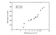
図7は、レーザー光(TiS(波長810nm)、80fs、40ショット)を入射した場合の、レーザー光のピークフルエンスとエッチレートとの関係を示す図である。Z=0mm(集光直径124ミクロン)の場合を丸印で、Z=4mm(集光直径95ミクロン)の場合を三角印で示す。図のように、エッチレートとピークフルエンスFpeak(対数)とはある関係がある。図7のような、レーザー光のピークフルエンスとエッチレートとの関係を計測すればある照射条件(レーザーの波長、パルス幅、繰り返し速度)において、エッチレートから対応するピークフルエンスを求めることができ、また逆にピークフルエンスから対応するエッチレートを決定できる。FIG. 7 is a diagram showing the relationship between the peak fluence of the laser beam and the etch rate when a laser beam (TiS (wavelength: 810 nm), 80 fs, 40 shots) is incident. The case of Z = 0 mm (condensing diameter of 124 microns) is indicated by a circle, and the case of Z = 4 mm (condensing diameter of 95 microns) is indicated by a triangle. As shown in the figure, there is a relationship between the etch rate and the peak fluence Fpeak (logarithm). As shown in FIG. 7, if the relationship between the peak fluence of the laser beam and the etch rate is measured, the corresponding peak fluence can be obtained from the etch rate under a certain irradiation condition (laser wavelength, pulse width, repetition rate). Conversely, the corresponding etch rate can be determined from the peak fluence.
図8は、直線偏光のレーザー光(TiS(波長810nm)、80fs)の照射を40ショット行った場合の、レーザー光のピークフルエンスと、表面の縞状の周期構造の有無などの表面状態との関係を示す図である。図の横軸はピークフルエンス(単位J/cm2)、縦軸は、レーザースポット跡の状態を「跡なし」「(跡があるが)周期構造なし」「周期構造形成」「周期構造崩れ(周期構造が中央から崩れる)」の4段階で示す。Z=0mmの場合を黒四角印で、Z=4mmの場合を白丸印で示す。図から、ピークフルエンスが2.7−7.7(J/cm2)の範囲である場合に、縞状の周期構造が確実に形成されることがわかる。「跡なし」と「(跡はあるが)周期構造なし」との境界となるピークフルエンスは、アブレーション閾値に相当する。図によれば、アブレーション閾値は、およそ2(J/cm2)である。FIG. 8 shows the peak fluence of the laser beam and the surface state such as the presence or absence of the periodic striped structure on the surface when 40 shots of linearly polarized laser beam (TiS (wavelength: 810 nm), 80 fs) are performed. It is a figure which shows a relationship. In the figure, the horizontal axis shows the peak fluence (unit: J / cm2 ), and the vertical axis shows the state of the laser spot trace “no trace” “(no trace) but no periodic structure” “periodic structure formation” “periodic structure collapse ( The periodic structure collapses from the center) ”. The case of Z = 0 mm is indicated by a black square mark, and the case of Z = 4 mm is indicated by a white circle mark. From the figure, it can be seen that when the peak fluence is in the range of 2.7 to 7.7 (J / cm2 ), the striped periodic structure is surely formed. The peak fluence that is the boundary between “no trace” and “no periodic structure (although there is a trace)” corresponds to the ablation threshold. According to the figure, the ablation threshold is approximately 2 (J / cm2 ).
(第4の実施の形態)
本実施の形態を、図9を参照して説明する。本実施の形態では、第3の実施の形態とは波長が異なるレーザー光を使用した場合に関して、第3の実施の形態と同様に、縞状の周期構造を形成することができる最適条件について説明する。(Fourth embodiment)
This embodiment will be described with reference to FIG. In the present embodiment, as to the case where laser light having a wavelength different from that of the third embodiment is used, the optimum condition for forming a striped periodic structure is described as in the third embodiment. To do.
図9は、直線偏光のレーザー光(Yb系KGW(波長1.03ミクロン)、200fs)の入射した場合の、レーザー光のエッチレートと、表面の縞状の周期構造の有無などの表面状態との関係を示す図である。図の横軸はエッチレート(単位nm/shot)、縦軸は、レーザースポット跡の状態を「跡なし」「(跡があるが)周期構造なし」「周期構造形成」「周期構造崩れ」の4段階で示す。「周期構造崩れ」とは周期構造が中央から崩れる場合を示し、周期構造は環状領域に存在する。図中、右下枠内に示したように、レーザーのパルスエネルギーと照射面積を変えることでフルエンスを変化させて作製した。パルスエネルギーが、28μJの場合を四角印で、60μJの場合を丸印で、110μJの場合を上向き三角印で、144μJの場合を下向き三角印で、186μJの場合を菱形印で、222μJの場合を左向き三角印で、272μJの場合を右向き三角印で示す。図に示されるように、エッチレートが約158−355(nm/shot)の範囲である場合に、縞状の周期構造が確実に形成されることがわかった。ピークフルエンスが1.5−5.0(J/cm2)である場合に、周期構造が確実に形成されることがわかった。また、アブレーション閾値は、およそ1.2(J/cm2)であった。FIG. 9 shows the state of the surface such as the etching rate of the laser beam and the presence or absence of a periodic structure of stripes on the surface when linearly polarized laser light (Yb-based KGW (wavelength 1.03 microns), 200 fs) is incident. It is a figure which shows the relationship. In the figure, the horizontal axis represents the etch rate (unit: nm / shot), and the vertical axis represents the state of the laser spot trace “no trace”, “(no trace) but no periodic structure”, “periodic structure formation”, “periodic structure collapse”. Shown in 4 stages. The “periodic structure collapse” means a case where the periodic structure collapses from the center, and the periodic structure exists in the annular region. As shown in the lower right frame in the figure, the fluence was changed by changing the pulse energy of the laser and the irradiation area. When the pulse energy is 28 μJ, it is a square mark, when it is 60 μJ, it is a circle mark, when it is 110 μJ, it is an upward triangle mark, when it is 144 μJ, it is a downward triangle mark, when it is 186 μJ, it is a diamond mark, and when it is 222 μJ The triangle pointing to the left indicates the case of 272 μJ by the triangle pointing to the right. As shown in the figure, it was found that when the etching rate is in the range of about 158 to 355 (nm / shot), the striped periodic structure is surely formed. It was found that the periodic structure was reliably formed when the peak fluence was 1.5 to 5.0 (J / cm2 ). The ablation threshold was approximately 1.2 (J / cm2 ).
数ショット以上の照射で周期構造が形成されていることから、周期構造が形成される条件として、エッチレートが縞の深さを超えないことが上限となる。エッチレートの下限は、実施の形態から判断して、縞の深さの1/5以上である。縞の周期から考えるとエッチレートは縞の周期の1/10から1/2の範囲にある。周期構造を明瞭に形成するには、エッチレートが縞の深さの1/5から1/2.5の範囲にあることが望ましい。 Since the periodic structure is formed by irradiation of several shots or more, the upper limit as a condition for forming the periodic structure is that the etch rate does not exceed the stripe depth. The lower limit of the etch rate is 1/5 or more of the stripe depth as judged from the embodiment. Considering the period of the stripes, the etching rate is in the range of 1/10 to 1/2 of the period of the stripes. In order to clearly form the periodic structure, it is desirable that the etch rate be in the range of 1/5 to 1 / 2.5 of the stripe depth.
また、第3及び第4の実施の形態から、[エッチレート/波長]は、第3実施例では132−280(nm/shot)/810nmは、0.16−0.34となり、第4の実施の形態では158−355(nm/shot)/1030nmは、0.15−0.34となる。このことから、フェムトレーザー光の波長が異なっていても、[エッチレート/波長]が、0.16−0.34の範囲である場合に、縞状の周期構造が確実に形成できる、といえる。 Further, from the third and fourth embodiments, the [etch rate / wavelength] of the third example is 132-280 (nm / shot) / 810 nm is 0.16-0.34. In the embodiment, 158 to 355 (nm / shot) / 1030 nm is 0.15 to 0.34. From this, it can be said that even if the wavelength of the femto laser beam is different, a striped periodic structure can be reliably formed when the [etch rate / wavelength] is in the range of 0.16-0.34. .
(第5の実施の形態)
本実施の形態を、図10及び11を参照して説明する。本実施の形態では、レーザー光の入射角度と縞状の周期構造との関係について調べた。(Fifth embodiment)
This embodiment will be described with reference to FIGS. In this embodiment mode, the relationship between the incident angle of laser light and the striped periodic structure was examined.
図10は、s偏光のレーザー光(中心波長810nm、パルス幅約80fs)をジルコニア系セラミックス基板に対して入射角θで入射した場合の、周期構造の状態と入射角との関係を示す図である。横軸は入射角θ(deg)、縦軸は形成された縞状の周期構造の周期(単位nm)である。縞状の周期の値は840−900nm程度であり、入射角θに対する周期の変化は、データのばらつきの範囲内であるので、周期は入射角に依存しないことがわかる。 FIG. 10 is a diagram showing the relationship between the state of the periodic structure and the incident angle when s-polarized laser light (center wavelength: 810 nm, pulse width: about 80 fs) is incident on the zirconia ceramic substrate at an incident angle θ. is there. The horizontal axis represents the incident angle θ (deg), and the vertical axis represents the period (unit: nm) of the formed striped periodic structure. The value of the striped period is about 840-900 nm, and the change in the period with respect to the incident angle θ is within the range of data variation, so that it can be seen that the period does not depend on the incident angle.
図11は、p偏光のレーザー光(中心波長810nm、パルス幅約80fs)をジルコニア系セラミックス基板に対して入射角θで入射した場合の、周期構造の状態と入射角との関係を示す図である。横軸は入射角θ(deg)、縦軸は形成された縞状の周期構造の周期(単位nm)である。縞状の周期の値は900−1040nm程度であり、入射角θに対する周期の変化は、p偏光の場合は、入射角が大きくなるにつれて周期が大きくなる傾向があることがわかる。ただし、p偏光の場合でも、角度に対する依存性は大きくないことがわかる。 FIG. 11 is a diagram showing the relationship between the state of the periodic structure and the incident angle when p-polarized laser light (center wavelength: 810 nm, pulse width: about 80 fs) is incident on the zirconia ceramic substrate at an incident angle θ. is there. The horizontal axis represents the incident angle θ (deg), and the vertical axis represents the period (unit: nm) of the formed striped periodic structure. The value of the striped period is about 900-1040 nm, and it can be seen that the change in the period with respect to the incident angle θ tends to increase as the incident angle increases in the case of p-polarized light. However, even in the case of p-polarized light, the dependence on the angle is not large.
本発明の場合は、従来報告されている偏光に直交する周期構造の角度依存性(例:特許文献2)とは、p偏光、s偏光ともに、異なる傾向を示している。 In the case of the present invention, both the p-polarized light and the s-polarized light have different tendencies from the conventionally reported angular dependence of the periodic structure orthogonal to the polarized light (eg, Patent Document 2).
(第6の実施の形態)
本実施の形態を、図12及び13を参照して説明する。本実施の形態では、レーザー光のパルス幅と縞状の周期構造との関係について調べた。本実施の形態では、レーザー光としてTiS(中心波長810nm、)を使用し、40ショット数で調べた。(Sixth embodiment)
This embodiment will be described with reference to FIGS. In this embodiment, the relationship between the pulse width of the laser beam and the striped periodic structure was examined. In this embodiment, TiS (center wavelength: 810 nm) is used as the laser beam, and the number of shots is 40.
図12は、レーザー光のパルス幅と、アブレーション加工された部分の面積や周期構造形成部分の面積との関係を示す図である。横軸はパルス幅(単位fs)、縦軸は、左は形成面積(単位μm2)を示し、右はレーザー照射跡の穴全体の面積に対する周期構造形成領域の面積の比(単位%)を示す。レーザー光のパルス幅を80から600fs程度までの条件で形成して測定した。測定したパルス幅の範囲600fsまでは、縞状の周期構造が形成されていることを確認した。パルス幅80fsで最適なフルエンス6.4J/cm2でレーザー光を入射した場合、縞状の周期構造が形成される面積は、パルス幅が長くなると、形成される穴の面積及び周期構造部分の面積が小さくなる傾向を示した。図中、実線の白丸印はレーザー光による穴の面積を示し、太線の黒丸印は縞状の周期構造が形成されている領域の面積を示す。図中、一点鎖線は、レーザー照射跡の穴全体の面積に対する周期構造形成領域の面積の比(単位%)を示す。比は、パルス幅が長くなるにつれて、小さくなる傾向を示した。図から、パルス幅が短い方が好ましいことがわかる。なお、図では、フルエンスを一定にして調べたが、パルス幅に対応して最適なフルエンスを適宜選択することにより、パルス幅の上限は、1ピコ秒に限定されない。FIG. 12 is a diagram showing the relationship between the pulse width of the laser beam and the area of the ablated portion or the area of the periodic structure forming portion. The horizontal axis shows the pulse width (unit: fs), the vertical axis shows the formation area (unit: μm2 ), and the right shows the ratio (unit:%) of the area of the periodic structure formation region to the area of the entire hole of the laser irradiation trace. Show. The pulse width of the laser beam was measured under the condition of about 80 to 600 fs. It was confirmed that a striped periodic structure was formed up to the measured pulse width range of 600 fs. When laser light is incident at an optimum fluence of 6.4 J / cm2 at a pulse width of 80 fs, the area where the striped periodic structure is formed is the area of the hole to be formed and the area of the periodic structure portion when the pulse width is increased. The area tended to decrease. In the drawing, solid white circles indicate the area of the hole by the laser beam, and thick black dots indicate the area of the region where the striped periodic structure is formed. In the figure, the alternate long and short dash line indicates the ratio (unit%) of the area of the periodic structure forming region to the area of the entire hole of the laser irradiation trace. The ratio tended to decrease as the pulse width increased. It can be seen from the figure that a shorter pulse width is preferable. In the figure, the fluence was checked to be constant, but the upper limit of the pulse width is not limited to 1 picosecond by appropriately selecting the optimum fluence corresponding to the pulse width.
図13は、レーザー光TiS(中心波長810nm、40ショット数)のパルス幅とエッチレートと周期構造形成状態との関係を示す図である。横軸はパルス幅(単位fs)、左の縦軸は、エッチレート(単位nm/shot)を示し、右は縞状の周期構造の周期(単位nm)を示す。レーザー光のパルス幅を80から600fs程度までの条件で測定した。測定した範囲600fsまでは周期構造が形成されているのを確認した。パルス幅80fsで最適なフルエンス6.4J/cm2のもとで形成した場合、パルス幅が長くなると、エッチレートが大きくなる傾向を示し、また、周期構造の周期が長くなる傾向を示した。実線の白丸印は、「レーザー光のビーム中央でのエッチレート」を示し、実線黒四角印は、「レーザー光のビーム内の縞状の周期構造が形成された領域のエッチレートの下限」を示す。ピークフルエンスでのエッチレートは、エッチレート(ピークフルエンス)=Dbottom/ショットと表すことができる。また、「ビーム内の縞状の周期構造が形成された領域のエッチレートの下限」は、エッチレート(下限)=DLL/ショットと表すことができる。実線黒三角印は縞状の周期を示す。パルス幅が80−550fsの場合、周期は900−1200nm程度であった。パルス幅を大きくすると、エッチレート(ピークフルエンス)とエッチレート(下限)が近づいている。これは、周期構造形成領域が狭くなっていることを意味する。FIG. 13 is a diagram showing the relationship between the pulse width of laser light TiS (center wavelength: 810 nm, number of 40 shots), etch rate, and periodic structure formation state. The horizontal axis represents the pulse width (unit: fs), the left vertical axis represents the etch rate (unit: nm / shot), and the right represents the period (unit: nm) of the striped periodic structure. The pulse width of the laser beam was measured under conditions of about 80 to 600 fs. It was confirmed that the periodic structure was formed up to the measured range of 600 fs. When the film was formed at an optimum fluence of 6.4 J / cm2 with a pulse width of 80 fs, the etch rate tended to increase as the pulse width increased, and the period of the periodic structure tended to increase. The solid white circle indicates the “etch rate at the center of the laser beam” and the solid black square indicates “the lower limit of the etch rate in the region where the striped periodic structure is formed in the laser beam”. Show. The etch rate at peak fluence can be expressed as etch rate (peak fluence) = Dbottom / shot. Further, “the lower limit of the etching rate of the region where the striped periodic structure in the beam is formed” can be expressed as etching rate (lower limit) = DLL / shot. Solid black triangle marks indicate a striped period. When the pulse width was 80-550 fs, the period was about 900-1200 nm. When the pulse width is increased, the etch rate (peak fluence) and the etch rate (lower limit) are approaching. This means that the periodic structure formation region is narrowed.
パルス幅は、フェムト秒レベルであれば縞状周期構造が形成されることがわかり、10fsから10ps程度まで可能である。500fs以下であればガウシアンビームでも周期構造が形成される面積の割合を50%以上に高くできる点から好ましい。また、100fs以下であれば、面積の割合を65%よりも大きくでき、より好ましい。 If the pulse width is a femtosecond level, it can be seen that a striped periodic structure is formed, and can be about 10 fs to 10 ps. If it is 500 fs or less, it is preferable because the ratio of the area where the periodic structure is formed can be increased to 50% or more even with a Gaussian beam. Moreover, if it is 100 fs or less, the ratio of an area can be larger than 65%, and it is more preferable.
(第7の実施の形態)
本実施の形態を、図14を参照して説明する。本実施の形態では、レーザー光のパルス幅と縞状の周期構造との関係について、レーザー光としてYb系(中心波長1.03μm)を使用して調べた。
Ybの1.03μmのレーザーを、ピークフルエンス4J/cm2、一か所に20ショット、繰り返し15kHzでジルコニア系セラミックスに照射した。パルス幅200fs、500fs、1ps、2ps、5psで実施し、底面に周期構造が形成されることを確認した。(Seventh embodiment)
This embodiment will be described with reference to FIG. In the present embodiment, the relationship between the pulse width of the laser beam and the striped periodic structure was examined using a Yb system (center wavelength: 1.03 μm) as the laser beam.
A Yb 1.03 μm laser was irradiated to zirconia ceramics at a peak fluence of 4 J / cm2 , 20 shots at one location, and repeatedly at 15 kHz. The pulse width was 200 fs, 500 fs, 1 ps, 2 ps, and 5 ps, and it was confirmed that a periodic structure was formed on the bottom surface.
図14は、レーザー光のパルス幅と、アブレーション加工された部分の面積や周期構造形成部分の面積との関係を示す図である。横軸はパルス幅(単位fs)、縦軸は、左は形成面積(単位μm2)を示し、右はレーザー照射跡の穴全体の面積に対する周期構造形成領域の面積の比「構造面積割合」を示す。レーザー光のパルス幅を200fsから5ps程度までの条件で形成して測定した。測定したパルス幅の範囲5psまでは、縞状の周期構造が形成されていることを確認した。縞状の周期構造が形成される面積は、パルス幅が長くなると、形成される穴の面積及び周期構造部分の面積が小さくなる傾向を示した。図中、実線の黒四角印はレーザー光による穴の面積「エッチ面積」を示し、実線の白丸印は縞状の周期構造が形成されている領域の面積を示す。図中、一点鎖線の三角印は、レーザー照射跡の穴全体の面積に対する周期構造形成領域の面積の比を示す。比は、パルス幅が長くなるにつれて、小さくなる傾向を示した。図から、パルス幅が短い方が周期構造の効率的な形成にとって有利であることがわかる。FIG. 14 is a diagram showing the relationship between the pulse width of the laser beam and the area of the ablated part or the area of the periodic structure forming part. The horizontal axis indicates the pulse width (unit: fs), the vertical axis indicates the formation area (unit: μm2 ), and the right indicates the ratio of the area of the periodic structure formation region to the area of the entire hole of the laser irradiation trace “structure area ratio” Indicates. The pulse width of the laser beam was measured under the condition of 200 fs to 5 ps. It was confirmed that a striped periodic structure was formed up to the measured pulse width range of 5 ps. As for the area where the striped periodic structure is formed, the area of the hole to be formed and the area of the periodic structure portion tend to decrease as the pulse width increases. In the figure, the solid black square mark indicates the area “etched area” of the hole by the laser beam, and the solid white circle mark indicates the area of the region where the striped periodic structure is formed. In the figure, a dot-and-dash triangle indicates the ratio of the area of the periodic structure forming region to the area of the entire hole of the laser irradiation trace. The ratio tended to decrease as the pulse width increased. From the figure, it can be seen that a shorter pulse width is advantageous for efficient formation of the periodic structure.
同様にパルス幅とエッチレートと周期構造形成状態との関係を調べた。レーザー光のパルス幅を200fsから5ps程度までの条件で測定した。パルス幅が長くなると、エッチレートが大きくなる傾向を示し、また、周期構造の周期が長くなる傾向を示した。パルス幅が200fsから5ps程度の場合、周期は1000−1400nm程度であった。パルス幅を大きくすると、エッチレート(ピークフルエンス)とエッチレート(下限)が近づいている。これは、周期構造形成領域が狭くなっていることを意味する。 Similarly, the relationship between the pulse width, the etch rate, and the periodic structure formation state was investigated. The pulse width of the laser beam was measured under conditions from 200 fs to about 5 ps. The longer the pulse width, the higher the etch rate, and the longer the period of the periodic structure. When the pulse width was about 200 fs to about 5 ps, the period was about 1000 to 1400 nm. When the pulse width is increased, the etch rate (peak fluence) and the etch rate (lower limit) are approaching. This means that the periodic structure formation region is narrowed.
(第8の実施の形態)
本実施の形態を、図15及び16を参照して説明する。本実施の形態では、レーザー光のショット数と縞状の周期構造との関係について調べた。本実施の形態では、レーザー光としてTiS(中心波長810nm、パルス幅80fs)を使用して調べた。フルエンスは6.6J/cm2とした。(Eighth embodiment)
This embodiment will be described with reference to FIGS. In this embodiment mode, the relationship between the number of shots of laser light and the striped periodic structure was examined. In the present embodiment, investigation was performed using TiS (center wavelength: 810 nm, pulse width: 80 fs) as laser light. The fluence was 6.6 J / cm2 .
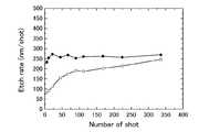
図15は、レーザー光のショット数と周期構造形成部分の面積と穴の深さの関係を示す図である。横軸はショット数、左の縦軸は、周期構造の形成面積(単位μm2)を示し、右の縦軸は穴の深さ(単位ミクロン)を示す。ショット数を6から340程度まで変化させて測定した。6から11ショットまでは、周期構造が不明瞭であったので「pre−structured」と呼び、図中×印で示す。図中22ショットのデータでは周期構造は明瞭であった。図中、実線白丸印はエッチングされた面積を示し、実線黒丸印は縞状周期構造形成部分の面積を示し、実線黒三角印は穴の深さを示す。ショット数の増加とともに、加工された面積が大きくなり、穴も深くなるが、縞状の周期構造の部分の面積は小さくなる傾向を示した。ショット数が340ショットまで周期構造が形成されていることを確認した。図では、外掃すると、400ショット以上にすると穴が深くなり底面には周期構造ができないか、底面に平らな面がなくなると考えられる。図から、12ショット以上400ショット未満であれば、いずれのショット数でも、縞状の周期構造が得られる。図から、最適なショット数は、周期構造が明瞭に形成されるショット数であれば、少ない方が望ましいことがわかる。最適な範囲は、20ショットから70ショット程度が好ましい。FIG. 15 is a diagram showing the relationship between the number of shots of laser light, the area of the periodic structure forming portion, and the hole depth. The horizontal axis represents the number of shots, the left vertical axis represents the formation area (unit μm2 ) of the periodic structure, and the right vertical axis represents the hole depth (unit micron). Measurement was performed by changing the number of shots from about 6 to about 340. From 6 to 11 shots, since the periodic structure was unclear, it is called “pre-structured” and is indicated by a cross in the figure. In the figure, the periodic structure was clear in the data of 22 shots. In the figure, solid white circles indicate the etched area, solid black circles indicate the area of the striped periodic structure forming portion, and solid black triangles indicate the depth of the holes. As the number of shots increased, the processed area increased and the hole deepened, but the area of the striped periodic structure tended to decrease. It was confirmed that the periodic structure was formed up to 340 shots. In the figure, when sweeping out, if the number of shots is increased to 400 shots or more, the hole becomes deep and a periodic structure is not formed on the bottom surface, or it is considered that there is no flat surface on the bottom surface. From the figure, a striped periodic structure can be obtained with any number of shots as long as it is 12 shots or more and less than 400 shots. From the figure, it can be seen that the optimum number of shots is desirable if it is the number of shots in which the periodic structure is clearly formed. The optimal range is preferably about 20 to 70 shots.
図16は、レーザー光のショット数とエッチレート(単位nm/shot)の関係を示す図である。横軸はショット数、縦軸は、エッチレートを示す。ショット数を6から340程度まで変化させて測定した。実線の黒丸印は、「レーザー光のビーム中央でのエッチレート」を示し、実線白四角印は、「レーザー光のビーム内の縞状の周期構造が形成された領域のエッチレートの下限」を示す。図中、エッチレートが、実線白四角印の線より大で、実線黒丸印の線より小である領域は、周期構造が形成されるエッチレートの有効な数値範囲を表している。ショット数が増加するにつれて、周期構造が形成されるエッチレート数値範囲が狭くなっていることがわかる。 FIG. 16 is a diagram showing the relationship between the number of shots of laser light and the etch rate (unit: nm / shot). The horizontal axis represents the number of shots, and the vertical axis represents the etch rate. Measurement was performed by changing the number of shots from about 6 to about 340. The solid black circle mark indicates “the etch rate at the center of the laser beam”, and the solid white square mark indicates “the lower limit of the etch rate in the region where the striped periodic structure is formed in the laser beam”. Show. In the drawing, the region where the etch rate is larger than the solid white square line and smaller than the solid black circle line represents an effective numerical range of the etch rate at which the periodic structure is formed. It can be seen that as the number of shots increases, the numerical range of the etch rate at which the periodic structure is formed becomes narrower.
(第9の実施の形態)
本実施の形態を、図17を参照して説明する。本実施の形態では、第8の実施の形態とは異なる波長のレーザー光を使用して、ショット数と縞状の周期構造との関係について調べた。本実施の形態では、レーザー光としてYb系KGW(中心波長約1ミクロン、パルス幅200fs)を使用して調べた。(Ninth embodiment)
This embodiment will be described with reference to FIG. In the present embodiment, the relationship between the number of shots and the striped periodic structure was examined using laser light having a wavelength different from that of the eighth embodiment. In this embodiment, Yb-based KGW (center wavelength: about 1 micron, pulse width: 200 fs) is used as the laser beam.
図17は、レーザー光のショット数と、周期構造形成部分の面積と、加工領域全体に対する周期構造形成領域の割合(Ratio of area)の関係を示す図である。横軸はショット数、左の縦軸は、周期構造の形成面積(単位μm2)を示し、右は加工領域全体に対する周期構造形成領域の割合(単位%)を示す。ショット数を10から90程度まで変化させて測定した。実線黒丸印は縞状の周期構造形成領域の面積であり、実線白丸印はアブレーションされた領域の全面積であり、点線三角印は、加工領域全体に対する周期構造形成領域の割合である。10ショットでは、縞状周期構造を確認できた。縞状の周期構造が形成された面積は50ショットで最大値となった。さらにショット数を増加させていくと、周期構造が形成されずにアブレーションのみ生じる周辺の領域が増大する。加工領域全体に対する周期構造形成領域の割合は、ショット数の増加につれて低下する。図から、周期構造が明瞭に形成され、かつ構造部分の面積も大きいという条件からは50ショットが最適である。また、面積が大きいのは、50、70、90ショットの順で、周期が明瞭な領域の割合が大きいのは、30、50、70ショットの順であることがわかる。図から、10から90ショットまで、いずれでも縞状の周期構造が得られるが、30ショットから70ショット程度の範囲が最適なショット数の範囲である。FIG. 17 is a diagram illustrating the relationship between the number of shots of laser light, the area of the periodic structure forming portion, and the ratio (Ratio of area) of the periodic structure forming region to the entire processing region. The horizontal axis represents the number of shots, the left vertical axis represents the formation area (unit μm2 ) of the periodic structure, and the right represents the ratio (unit%) of the periodic structure formation region to the entire processing region. Measurement was performed by changing the number of shots from about 10 to about 90. Solid black circles indicate the area of the striped periodic structure formation region, solid white circles indicate the total area of the ablated region, and dotted triangles indicate the ratio of the periodic structure formation region to the entire processing region. In 10 shots, a striped periodic structure was confirmed. The area where the striped periodic structure was formed reached the maximum value at 50 shots. As the number of shots is further increased, the peripheral area where only ablation occurs without forming the periodic structure increases. The ratio of the periodic structure formation region to the entire processing region decreases as the number of shots increases. From the figure, 50 shots are optimal from the condition that the periodic structure is clearly formed and the area of the structure portion is large. Further, it can be seen that the area is large in the order of 50, 70, and 90 shots, and the ratio of the region having a clear cycle is large in the order of 30, 50, and 70 shots. From the figure, it is possible to obtain a striped periodic structure in any of 10 to 90 shots, but the range of about 30 to 70 shots is the optimum number of shots.
(第10の実施の形態)
これまでの実施の形態では、ジルコニア系セラミックスとして、具体的には3mol%Y2O3ジルコニアを使用して形成加工の計測を行ったものを示したが、他の組成でも、同様の結果を示すことを確認した。4mol%、8mol%、10mol%のY2O3を含むジルコニア(それぞれ、4Y、8Y、10Yと呼ぶ)、3mol%のY2O3と20%のAl2O3を含むジルコニア(3Y20Aと呼ぶ)に対し、直線偏光のレーザー光(中心波長810nm、パルス幅100fs、繰り返し560Hz)を、ピークフルエンス6.9J/cm2で40ショット照射した。いずれの場合にも直線偏光の偏光方向に平行な縞状の周期構造が観測された。観測された構造の周期は、4Y、8Y、10Yに対して、900nm−910nm程度であった。また、3Y20Aに対して、約940nmであった。3Y、4Y、8Y、10Y、3Y20Aの順にエッチレートが大きくなる傾向が見られた。(Tenth embodiment)
In the embodiments so far, as the zirconia-based ceramics, specifically, 3 mol% Y2 O3 zirconia was used to measure the forming process. However, similar results were obtained with other compositions. Confirmed to show. Zirconia containing 4 mol%, 8 mol%, 10 mol% Y2 O3 (referred to as 4Y, 8Y, 10Y, respectively), zirconia containing 3 mol% Y2 O3 and 20% Al2 O3 (referred to as 3Y20A) ) Was irradiated with 40 shots of linearly polarized laser light (center wavelength 810 nm,
なお、表面加工の加工対象の材料として、金属の場合について調べた。ジルコニア表面に一部金属(Al)を被覆して、本実施の形態と同様の直線偏光のレーザー光を照射したところ、金属面では、偏光方向に垂直に縞が形成され、ジルコニア表面では、偏光に平行に縞が形成された。このことから、本実施の形態は、ジルコニア系セラミックスにおいて有効な加工方法であることがわかる。 In addition, it investigated about the case of a metal as a material of the surface processing object. When the surface of the zirconia is partially coated with metal (Al) and irradiated with the linearly polarized laser beam similar to the present embodiment, stripes are formed perpendicular to the polarization direction on the metal surface, and polarized light is formed on the zirconia surface. A stripe was formed in parallel with each other. From this, it can be seen that the present embodiment is an effective processing method in zirconia ceramics.
(第11の実施の形態)
本実施の形態では、レーザー光による表面加工装置において、ビームの強度分布を均一化する光学素子を設けてレーザー光を照射した場合について説明する。
レーザー光照射の空間分布は、図2に示したように、ガウス分布であるが、ビームの強度分布を均一化する光学素子を設けて、ビームの強度分布が均一化されたレーザー光を照射した場合、穴の深さが照射部分でほぼ均一となり、アブレーションされた底面の90%以上の領域に周期構造が形成された。(Eleventh embodiment)
In the present embodiment, a case where a laser beam is irradiated with an optical element that makes the beam intensity distribution uniform in a surface processing apparatus using laser light will be described.
As shown in FIG. 2, the spatial distribution of the laser beam irradiation is a Gaussian distribution. However, an optical element for uniformizing the beam intensity distribution is provided, and the laser beam with the uniform beam intensity distribution is irradiated. In this case, the depth of the hole was almost uniform at the irradiated portion, and a periodic structure was formed in a region of 90% or more of the ablated bottom surface.
(第12の実施の形態)
本実施の形態では、縞状の周期構造を大面積化する方法について説明する。(Twelfth embodiment)
In this embodiment, a method for increasing the area of a striped periodic structure will be described.
レーザー光を連続的にスキャンした場合について観測すると、周期構造がビームの裾で破壊された。従来技術のようにレーザー光を連続走査(スキャン)すると、ビームを連続的に移動した部分では周期構造が観測されない。一方、ビームを停止した場所では、スポットの中央部分に周期構造が観測された。レーザー光の走査方向を、レーザー光の直線偏光方向と同じ方向とした場合も、直線偏光方向に直交する方向とした場合も、いずれも、同じ結果であった。これは一か所あたりの照射数を40ショット程度の場合には照射位置のずれの量が、ビームの裾で構造が壊される長さに比較して小さいためにおこる。 When the laser beam was scanned continuously, the periodic structure was destroyed at the bottom of the beam. When the laser beam is continuously scanned (scanned) as in the prior art, the periodic structure is not observed in the portion where the beam is continuously moved. On the other hand, at the place where the beam was stopped, a periodic structure was observed at the center of the spot. Both the scanning direction of the laser light was the same as the linear polarization direction of the laser light and the direction orthogonal to the linear polarization direction was the same result. This is because when the number of irradiations per place is about 40 shots, the amount of displacement of the irradiation position is small compared to the length at which the structure is broken at the bottom of the beam.
レーザー光を、フラットトップな強度プロファイルを有するレーザービームに、光学系により整形して用いる場合は、スキャン方式でも周期構造を作製することができる。フラットトップの場合で、必要なショット数が少ない場合あるいはビームサイズが大きい場合に適している。 When laser light is shaped into a laser beam having a flat-top intensity profile by using an optical system, a periodic structure can be produced even by a scanning method. In the case of a flat top, it is suitable when the number of shots required is small or the beam size is large.
理想的なフラットトップビームであればスキャン方式での大面積化が可能であるが、実際のビームでは有限の幅を持った弱い強度部分を有するため、複数ショットの照射が必要な周期構造形成においては、スキャン方式による周期構造の形成は周期構造が形成された部分の面積比率の低下をもたらす。図18に、簡略化のために四角いレーザービームの形状のフラットトップビームを示し、図19に、フラットトップビームを使用してスキャンして周期構造の大面積化をする方法を示す。図19に示すように、ビームを左から右に1ショットずつずらしながら照射する場合(スキャン照射)を考える。図中縦縞が周期構造が形成される領域であり、周囲の部分が周期構造が形成されずにアブレーションされる領域である。例えば一か所にNショットの照射が必要であり、走査方向のアブレーションされる長さをL1、端の部分で構造が形成されない片側の端の長さをL2とし、二つの比をC1=L2/L1とおく。照射位置を連続的にスキャンしながら、一か所に等価的にNショット照射するときには1ショットあたりのビームのずれはL1/Nであり、周期構造が形成される横方向の長さは、L3=(L1/N)−L2 で与えられる。L3が正の場合には、構造が残り、L3が負の場合には、構造はスキャンされたビームの肩で崩される。An ideal flat-top beam can increase the area by scanning, but the actual beam has a weak intensity part with a finite width, so in the formation of a periodic structure that requires multiple shot irradiation The formation of the periodic structure by the scanning method brings about a reduction in the area ratio of the portion where the periodic structure is formed. FIG. 18 shows a flat top beam in the form of a square laser beam for simplification, and FIG. 19 shows a method of increasing the area of the periodic structure by scanning using the flat top beam. As shown in FIG. 19, consider a case where a beam is irradiated while being shifted from left to right by one shot (scan irradiation). In the figure, vertical stripes are regions in which the periodic structure is formed, and surrounding portions are regions that are ablated without forming the periodic structure. For example, it is necessary to irradiate N shots at one place, the length to be ablated in the scanning direction is L1 , the length ofone end where the structure is not formed at the end is L2, and the ratio of the two is C1 = L2 / L1 When N shots are equivalently irradiated to one place while continuously scanning the irradiation position, the beam shift per shot is L1 / N, and the lateral length in which the periodic structure is formed is L3 = (L1 / N) −L2 If L3 is positive, the structure remains, and if L3 is negative, the structure is collapsed at the shoulder of the scanned beam.
構造が形成される部分の横方向の割合は、図19の点線で囲った部分(ショット1の上にショット2、3、4が重なっている部分)で考えると、Rarea=1−N*C1 で与えられる。例えば、C1=0.1の場合、一か所に4ショット照射するようにスキャンすると(N=4)、Rarea=0.6となり、60%の横方向の割合に構造が残る。縦方向の肩の効果を考慮すると全体の面積に対する形成される割合は48%となる。The ratio in the horizontal direction of the portion where the structure is formed is Rarea = 1−N * when considering the portion surrounded by the dotted line in FIG. 19 (the portion where
L3>0の条件を満たすには、L1が大きいこと、L2が小さいこと、Nが小さいことが望ましい。レーザーのパワーでL1の大きさは決まり、ビームの均一性や形状でL2が決まり、Nはレーザーのフルエンスやパルス幅に依存する。In order to satisfy the condition of L3 > 0, it is desirable that L1 is large, L2 is small, and N is small. The size of L1 is determined by the power of the laser, L2 is determined by the uniformity and shape of the beam, and N depends on the fluence and pulse width of the laser.
本実施の形態では、周期構造をジルコニア基材表面に広く形成するために、連続的ではなく、又は連続的に、レーザースポットごとにレーザー光を走査する。レーザースポットごとにレーザー光を移動させて走査するとは、例えば、ガウシアンビームや均一な硬度分布を持つビームあるいは強度分布を均一化したビームを、同一カ所に1回以上所定の回数照射することで照射部分全体に構造を作成したのち、いくらかの重なりを持つようにビームをずらして、あるいは隣り合う位置又はそれ以上間隔をあけてビームをずらして、同様の照射により構造を作成すること、を繰り返すことをいう。隣り合う位置又はそれ以上間隔をあけてビームをずらす方式は、スタンプ方式とはステップ方式などと呼ぶことができる。また、いくらかの重なりを持つようにビームをずらす方式は、ほぼ連続的な走査方式である。 In the present embodiment, in order to widely form the periodic structure on the surface of the zirconia substrate, the laser beam is scanned for each laser spot instead of continuously or continuously. Scanning by moving the laser beam for each laser spot is, for example, irradiating a Gaussian beam, a beam with a uniform hardness distribution, or a beam with a uniform intensity distribution by irradiating the same spot at least once a predetermined number of times. After creating the structure for the entire part, repeat the process of shifting the beam so that there is some overlap, or shifting the beam at adjacent positions or more apart and creating the structure by similar irradiation. Say. The method of shifting the beam at an interval between adjacent positions or more can be called a step method or the like as a stamp method. Further, the method of shifting the beam so as to have some overlap is a substantially continuous scanning method.
直線偏光のレーザービームを、均一な分布が広くなるように調整し、一カ所に40ショットごと照射し、次にスポット径以上の距離を移動させて、既に形成したスポットと重ならない位置で、次のレーザー光照射をした。レンズ系で構成されるビーム均一化素子と縦横の開口サイズが可変なスリットにより均一な空間強度分布を抜き出し、照射部分に結像光学系を用いて像転送した。50ミクロンステップでXY方向にタイル状に照射し、10mm×10mmの面積を加工した。周期構造が形成されている部分の面積の割合が全体の面積の50%のものが得られた。 Adjust the linearly polarized laser beam so that the uniform distribution is wide, irradiate 40 shots at one spot, then move the distance more than the spot diameter, and at the position where it does not overlap the already formed spot The laser beam was irradiated. A uniform spatial intensity distribution was extracted by a beam uniformizing element composed of a lens system and slits with variable vertical and horizontal aperture sizes, and an image was transferred to the irradiated portion using an imaging optical system. Irradiation was tiled in the XY direction at 50 micron steps to process an area of 10 mm × 10 mm. The ratio of the area of the portion where the periodic structure was formed was 50% of the total area.
レーザー光の結像による空間強度分布の整形について説明する。レーザー光を、レンズ系や回折光学素子で構成される空間強度分布整形光学素子を介して、スリットやピンホールで構成される空間制限マスクに集光し、空間制限マスクにより形状(三角、四角、五角形、六角形、楕円形等)が調整されたレーザー光を、結像用光学系により、照射サンプルであるジルコニア形セラミックスに倍率を調整して照射する。空間分布の制御には、回折効果と干渉を利用するビーム整形光学素子や液晶空間変調器等を利用するビーム整形器を用いてもよい。スリット等で空間的な形状を制御しその形状を像転送する方式において、空間的な形状は長方形以外にも三角形、五角形、六角形、などの多角形を用いることで平面のみならず球面などの3次元平面への隙間のない加工が実現できる。このように、レーザー光照射スポットの周期構造生成部分のみを照射可能な様に三角、四角、六角等の形状のピンホールやスリットに集光し、ピンホールの像を転送できる光学系でジルコニア系セラミックスに連続照射し、各々生成した周期構造のスポットを効率良く敷き詰めることができる。ビームの照射位置を変化するには、照射ビームと被照射サンプルの相対的な位置を変化させればよく、ビームの進行方向を変化させるガルバノミラーなどのビーム偏向装置を用いる方法、あるいは被照射サンプルの空間位置を移動するステージを用いる方法、またはこれらを組み合わせる方法がある。被照射サンプルをステージで移動する方法は高精度な制御が可能であり、ガルバノミラーなどのビーム偏向装置を用いる方法はステージを用いる方法に比較しより高速な位置決めが可能である。大面積を加工する場合にはガルバノミラーなどのビーム偏向装置を用いることが望ましい。 The shaping of the spatial intensity distribution by laser light imaging will be described. The laser light is condensed on a space limiting mask composed of slits and pinholes via a spatial intensity distribution shaping optical element composed of a lens system and a diffractive optical element, and the shape (triangle, square, A laser beam with an adjusted pentagonal shape, hexagonal shape, elliptical shape, etc. is irradiated onto the zirconia-shaped ceramics, which is an irradiation sample, by adjusting the magnification by an imaging optical system. For the control of the spatial distribution, a beam shaper using a beam shaping optical element using a diffraction effect and interference, a liquid crystal spatial modulator, or the like may be used. In the method of controlling the spatial shape with slits etc. and transferring the image, the spatial shape is not only a rectangle but also a polygon such as a triangle, pentagon, hexagon, etc. Processing without gaps on a three-dimensional plane can be realized. In this way, it is an optical system that can focus on a pinhole or slit in the shape of triangle, square, hexagon, etc. so that only the periodic structure generation part of the laser light irradiation spot can be irradiated, and transfer the pinhole image to the zirconia system By continuously irradiating ceramics, it is possible to efficiently spread the spots of the generated periodic structures. To change the irradiation position of the beam, the relative position between the irradiation beam and the sample to be irradiated may be changed. A method using a beam deflecting device such as a galvanometer mirror that changes the traveling direction of the beam, or the sample to be irradiated There are a method of using a stage that moves the spatial position of these, or a method of combining them. A method of moving the sample to be irradiated on the stage can be controlled with high accuracy, and a method using a beam deflecting device such as a galvanometer mirror can be positioned faster than a method using a stage. When processing a large area, it is desirable to use a beam deflecting device such as a galvanometer mirror.
Yb系の1.03μm、200fsのレーザーを用いて、ガウシアンビームでほぼ円形にビームを照射したときに形成される穴の直径が30ミクロンの時に20μmステップで縦横にビームをずらしながら、各位置に10ショット照射して1mm角の面積にわたり周期構造を形成した。加工部面積に対し周期構造が形成されている部分の面積割合が50%を超えるものが得られた。また、ビーム形状を整形することによりさらに高い面積割合を実現できる。 Using a Yb-based 1.03 μm, 200 fs laser, when the diameter of the hole formed when irradiating a Gaussian beam in a substantially circular shape is 30 microns, the beam is shifted vertically and horizontally in steps of 20 μm to each position. A periodic structure was formed over an area of 1 mm square by irradiation with 10 shots. The thing in which the area ratio of the part in which the periodic structure is formed with respect to the processed part area exceeds 50% was obtained. Further, a higher area ratio can be realized by shaping the beam shape.
上記実施形態等で示した例は、発明を理解しやすくするために記載したものであり、この形態に限定されるものではない。 The example shown by the said embodiment etc. was described in order to make invention easy to understand, and is not limited to this form.
本発明は、ジルコニア系セラミックスの表面に微細な周期構造を実現するものであり、生体親和性を持って骨等と結合させる必要がある生体材料への適用、ジェットエンジン内壁等の耐熱構造材料への適用、酸素センサー等への適用が可能であるので、産業上有用である。 The present invention realizes a fine periodic structure on the surface of zirconia-based ceramics, and is applied to biomaterials that need to be combined with bone or the like with biocompatibility, to heat-resistant structural materials such as jet engine inner walls. Therefore, the present invention is industrially useful.
1 レーザー発生装置
2 パワー制御装置
3 偏光状態制御装置
4 ビーム整形装置
5 集光レンズ
6 照射用ステージDESCRIPTION OF
Claims (7)
Translated fromJapanese直線偏光の超短パルスレーザー光を前記セラミックス表面に照射することにより、前記直線偏光の偏光方向に平行な縞状の凹凸を、レーザー光のスポット内に形成することを特徴とするジルコニア系セラミックスの表面構造形成方法。A method for forming a surface structure of a zirconia ceramic surface,
By irradiating the surface of the ceramic with linearly polarized ultrashort pulse laser light, striped irregularities parallel to the polarization direction of the linearly polarized light are formed in the laser light spot. Surface structure forming method.
円偏光の超短パルスレーザー光を前記セラミックス表面に照射することにより、網目状凸部及び点状凹部を周期的に形成することを特徴とするジルコニア系セラミックスの表面構造形成方法。A method for forming a surface structure of a zirconia ceramic surface,
A method for forming a surface structure of a zirconia-based ceramic, characterized in that a net-like convex portion and a dot-like concave portion are periodically formed by irradiating the ceramic surface with circularly polarized ultrashort pulse laser light.
Applications Claiming Priority (3)
| Application Number | Priority Date | Filing Date | Title |
|---|---|---|---|
| JP2014185472 | 2014-09-11 | ||
| JP2014185472 | 2014-09-11 | ||
| PCT/JP2015/075732WO2016039419A1 (en) | 2014-09-11 | 2015-09-10 | Method for forming surface structure of zirconia-based ceramic, and zirconia-based ceramic |
Related Child Applications (1)
| Application Number | Title | Priority Date | Filing Date |
|---|---|---|---|
| JP2019118665ADivisionJP6858987B2 (en) | 2014-09-11 | 2019-06-26 | Zirconia ceramics |
Publications (2)
| Publication Number | Publication Date |
|---|---|
| JPWO2016039419A1true JPWO2016039419A1 (en) | 2017-08-31 |
| JP6590343B2 JP6590343B2 (en) | 2019-10-16 |
Family
ID=55459163
Family Applications (3)
| Application Number | Title | Priority Date | Filing Date |
|---|---|---|---|
| JP2016547502AActiveJP6590343B2 (en) | 2014-09-11 | 2015-09-10 | Method for forming surface structure of zirconia ceramics and zirconia ceramics |
| JP2019118665AActiveJP6858987B2 (en) | 2014-09-11 | 2019-06-26 | Zirconia ceramics |
| JP2021044691AActiveJP7111392B2 (en) | 2014-09-11 | 2021-03-18 | zirconia ceramics |
Family Applications After (2)
| Application Number | Title | Priority Date | Filing Date |
|---|---|---|---|
| JP2019118665AActiveJP6858987B2 (en) | 2014-09-11 | 2019-06-26 | Zirconia ceramics |
| JP2021044691AActiveJP7111392B2 (en) | 2014-09-11 | 2021-03-18 | zirconia ceramics |
Country Status (4)
| Country | Link |
|---|---|
| US (1) | US10774003B2 (en) |
| EP (1) | EP3202752B1 (en) |
| JP (3) | JP6590343B2 (en) |
| WO (1) | WO2016039419A1 (en) |
Families Citing this family (12)
| Publication number | Priority date | Publication date | Assignee | Title |
|---|---|---|---|---|
| JP2822502B2 (en) | 1989-10-31 | 1998-11-11 | 株式会社島津製作所 | Material testing machine |
| CN105935837A (en)* | 2016-05-30 | 2016-09-14 | 湖北工业大学 | Laser texturing method for improving adhesive force of surface of weathering resistant steel |
| AU2017356025B2 (en)* | 2016-11-10 | 2020-05-14 | Nantoh. Co., Ltd | Biological tissue rootage face, implant, method for forming biological tissue rootage face, and method for producing implant |
| TWI828768B (en)* | 2018-09-27 | 2024-01-11 | 日商大賽璐塑膠股份有限公司 | Non-magnetic ceramic shaped body with roughened surface and manufacturing method thereof |
| JP6928741B2 (en)* | 2018-09-27 | 2021-09-01 | ダイセルミライズ株式会社 | Carbide-based non-magnetic ceramic molded body having a roughened structure on the surface and its manufacturing method |
| EP3811896B1 (en)* | 2019-10-22 | 2024-05-01 | Nadja Rohr | Dental implant |
| CN111168232B (en)* | 2020-02-07 | 2021-04-20 | 吉林大学 | A method for nanometer precision fabrication using femtosecond laser |
| EP4110547B1 (en)* | 2020-02-28 | 2025-01-15 | Katholieke Universiteit Leuven KU Leuven Research & Development | Method of selective phase removal in nanocomposite comprising at least first and second phases |
| JP7698840B2 (en)* | 2021-09-03 | 2025-06-26 | 東ソー株式会社 | Zirconia sintered body and its manufacturing method |
| EP4457049A4 (en) | 2021-12-29 | 2025-10-01 | Plasmatex Llc | PULSED LASER PROCESSING OF MEDICAL DEVICES |
| US12319625B1 (en)* | 2023-05-18 | 2025-06-03 | Honeywell Federal Manufacturing & Technologies, Llc | Ultrashort pulse laser surface treatment of ceramics |
| CN117550922A (en)* | 2023-11-10 | 2024-02-13 | 天津医科大学口腔医院 | Method for increasing surface adhesiveness of zirconia by femtosecond laser |
Citations (7)
| Publication number | Priority date | Publication date | Assignee | Title |
|---|---|---|---|---|
| JPH0845114A (en)* | 1994-08-03 | 1996-02-16 | Ricoh Co Ltd | Optical disc master exposure device |
| JPH0948684A (en)* | 1995-08-03 | 1997-02-18 | Denso Corp | Improved processing of ceramic and device therefor |
| JP2003057422A (en)* | 2001-08-17 | 2003-02-26 | Japan Science & Technology Corp | Fabrication method of periodic fine structure by femtosecond laser irradiation |
| JP2003211400A (en)* | 2002-01-22 | 2003-07-29 | Japan Science & Technology Corp | Fine processing method using ultra-short pulse laser and processed product |
| JP2008170679A (en)* | 2007-01-11 | 2008-07-24 | Ricoh Co Ltd | Beam splitting element, beam interference optical system, and beam interference exposure apparatus |
| JP2008216911A (en)* | 2007-03-07 | 2008-09-18 | Ricoh Co Ltd | Optical scanning device and image forming device |
| US20090035723A1 (en)* | 2007-08-03 | 2009-02-05 | Claus Daniel | Material with a repetitive pattern of micro-features for application in a living organism and method of fabrication |
Family Cites Families (8)
| Publication number | Priority date | Publication date | Assignee | Title |
|---|---|---|---|---|
| JPH0763950A (en)* | 1992-09-29 | 1995-03-10 | Tosoh Corp | Zirconia optical fiber connector parts |
| US6057525A (en)* | 1995-09-05 | 2000-05-02 | United States Enrichment Corporation | Method and apparatus for precision laser micromachining |
| WO2004035255A1 (en)* | 2002-09-27 | 2004-04-29 | Nec Machinery Corporation | Cyclic structure formation method and surface treatment method |
| JP4440270B2 (en) | 2004-09-06 | 2010-03-24 | キヤノンマシナリー株式会社 | Method for improving adhesion of thin film |
| JP5097354B2 (en)* | 2006-03-20 | 2012-12-12 | 京セラメディカル株式会社 | Biological member and method for producing the same |
| CN100581708C (en)* | 2008-04-25 | 2010-01-20 | 河北工业大学 | Application of femtosecond laser in titanium or titanium alloy implantation material surface treatment |
| US9993895B2 (en)* | 2009-03-30 | 2018-06-12 | Boegli-Gravures Sa | Method and device for structuring the surface of a hard material coated solid body by means of a laser |
| JP2014048526A (en)* | 2012-08-31 | 2014-03-17 | Dexerials Corp | Optical body, display device, input device, and electronic apparatus |
- 2015
- 2015-09-10USUS15/510,198patent/US10774003B2/enactiveActive
- 2015-09-10WOPCT/JP2015/075732patent/WO2016039419A1/enactiveApplication Filing
- 2015-09-10EPEP15839233.2Apatent/EP3202752B1/enactiveActive
- 2015-09-10JPJP2016547502Apatent/JP6590343B2/enactiveActive
- 2019
- 2019-06-26JPJP2019118665Apatent/JP6858987B2/enactiveActive
- 2021
- 2021-03-18JPJP2021044691Apatent/JP7111392B2/enactiveActive
Patent Citations (7)
| Publication number | Priority date | Publication date | Assignee | Title |
|---|---|---|---|---|
| JPH0845114A (en)* | 1994-08-03 | 1996-02-16 | Ricoh Co Ltd | Optical disc master exposure device |
| JPH0948684A (en)* | 1995-08-03 | 1997-02-18 | Denso Corp | Improved processing of ceramic and device therefor |
| JP2003057422A (en)* | 2001-08-17 | 2003-02-26 | Japan Science & Technology Corp | Fabrication method of periodic fine structure by femtosecond laser irradiation |
| JP2003211400A (en)* | 2002-01-22 | 2003-07-29 | Japan Science & Technology Corp | Fine processing method using ultra-short pulse laser and processed product |
| JP2008170679A (en)* | 2007-01-11 | 2008-07-24 | Ricoh Co Ltd | Beam splitting element, beam interference optical system, and beam interference exposure apparatus |
| JP2008216911A (en)* | 2007-03-07 | 2008-09-18 | Ricoh Co Ltd | Optical scanning device and image forming device |
| US20090035723A1 (en)* | 2007-08-03 | 2009-02-05 | Claus Daniel | Material with a repetitive pattern of micro-features for application in a living organism and method of fabrication |
Non-Patent Citations (5)
| Title |
|---|
| FUMIYA WATANABE ET AL.: "Ablation of crystalline oxides by infrared femtosecond laser pulses", J. APPL. PHYS., vol. 100, JPN6015043537, 2006, pages 083519 - 1, ISSN: 0003916169* |
| J. IHLEMANN ET AL.: "Nanosecond and femtosecond excimer-laser ablation of oxide ceramics", APPL. PHYS. A, vol. 60, JPN6015043543, 1995, pages 411 - 417, ISSN: 0003916172* |
| K. KAWAMURA ET AL.: "Fabrication of surface relief gratings on transparent dielectric materials by two-beam holographic m", APPLIED PHYSICS B, vol. Volume 71, Issue 1, JPN6015043539, July 2000 (2000-07-01), pages 119 - 121, ISSN: 0003916170* |
| S. HEIROTH ET AL.: "Laser ablation characteristics of yttria-doped zirconia in the nanosecond and femtosecond regimes", J. APPL. PHYS., vol. 107, JPN7015002984, 2010, pages 014908 - 1, ISSN: 0003916171* |
| 川原公介 ほか: "フェムト秒レーザによる表面微細突起構造の形成", 2006年度 精密工学会秋季大会 学術講演会講演論文集, JPN6015043544, 4 September 2006 (2006-09-04), pages 881 - 882, ISSN: 0003916173* |
Also Published As
| Publication number | Publication date |
|---|---|
| US20170260100A1 (en) | 2017-09-14 |
| EP3202752A4 (en) | 2018-06-13 |
| EP3202752B1 (en) | 2023-08-23 |
| JP6590343B2 (en) | 2019-10-16 |
| JP6858987B2 (en) | 2021-04-14 |
| US10774003B2 (en) | 2020-09-15 |
| JP2019206471A (en) | 2019-12-05 |
| EP3202752A1 (en) | 2017-08-09 |
| JP2021104927A (en) | 2021-07-26 |
| JP7111392B2 (en) | 2022-08-02 |
| WO2016039419A1 (en) | 2016-03-17 |
Similar Documents
| Publication | Publication Date | Title |
|---|---|---|
| JP6590343B2 (en) | Method for forming surface structure of zirconia ceramics and zirconia ceramics | |
| Vorobyev et al. | Femtosecond laser structuring of titanium implants | |
| Carvalho et al. | Femtosecond laser microstructuring of alumina toughened zirconia for surface functionalization of dental implants | |
| Zwahr et al. | Fabrication of multifunctional titanium surfaces by producing hierarchical surface patterns using laser based ablation methods | |
| Tiainen et al. | Novel laser surface texturing for improved primary stability of titanium implants | |
| CN104591549B (en) | A kind of method that use femto-second laser pulse sequence processes microarray in glass surface | |
| US20050211680A1 (en) | Systems and methods for laser texturing of surfaces of a substrate | |
| Roitero et al. | A parametric study of laser interference surface patterning of dental zirconia: Effects of laser parameters on topography and surface quality | |
| US20040000540A1 (en) | Laser texturing of surfaces for biomedical implants | |
| Li et al. | Precise micromachining of yttria-tetragonal zirconia polycrystal ceramic using 532 nm nanosecond laser | |
| US20130138103A1 (en) | Electrosurgical unit with micro/nano structure and the manufacturing method thereof | |
| US20090035723A1 (en) | Material with a repetitive pattern of micro-features for application in a living organism and method of fabrication | |
| JP7120576B2 (en) | Method for controlling wettability of metal surface | |
| Schelle et al. | Ultrashort pulsed laser (USPL) application in dentistry: basic investigations of ablation rates and thresholds on oral hard tissue and restorative materials | |
| Oyane et al. | Biomimetic apatite coating on yttria-stabilized tetragonal zirconia utilizing femtosecond laser surface processing | |
| Ferraris et al. | Laser surface texturing of Ti-cp and Ti6Al4V alloy for the improvement of fibroblast adhesion and alignment and the reduction of bacterial adhesion | |
| TWI548391B (en) | Bone implant and manufacturing method thereof | |
| Li et al. | Fatigue behavior of zirconia with microgrooved surfaces produced using femtosecond laser | |
| KR20110091257A (en) | Dental implants with increased surface friction coefficient Laser surface treatment method and dental implants treated by the method | |
| CN109574706B (en) | A kind of silicon nitride ceramic with surface-modifiable micro-nano structure and processing method thereof | |
| Vorobyev et al. | Femtosecond laser surface structuring of biocompatible metals | |
| Garcia-de-Albeniz et al. | Tailoring cell behavior and antibacterial properties on zirconia biomaterials through femtosecond laser-induced micropatterns and nanotopography | |
| Colpitts et al. | Laser Processing of Silicon for Synthesis of Better | |
| Berger et al. | Multiple-beam laser patterning on aluminum oxide, zirconium oxide, and hydroxyapatite ceramic materials using a microlens array | |
| Götze et al. | Processing of polyamide electrospun nanofibers with picosecond UV-laser irradiation |
Legal Events
| Date | Code | Title | Description |
|---|---|---|---|
| A521 | Request for written amendment filed | Free format text:JAPANESE INTERMEDIATE CODE: A523 Effective date:20170301 | |
| A521 | Request for written amendment filed | Free format text:JAPANESE INTERMEDIATE CODE: A523 Effective date:20170301 | |
| A621 | Written request for application examination | Free format text:JAPANESE INTERMEDIATE CODE: A621 Effective date:20170321 | |
| A131 | Notification of reasons for refusal | Free format text:JAPANESE INTERMEDIATE CODE: A131 Effective date:20180509 | |
| A521 | Request for written amendment filed | Free format text:JAPANESE INTERMEDIATE CODE: A523 Effective date:20180620 | |
| A131 | Notification of reasons for refusal | Free format text:JAPANESE INTERMEDIATE CODE: A131 Effective date:20181114 | |
| A521 | Request for written amendment filed | Free format text:JAPANESE INTERMEDIATE CODE: A523 Effective date:20181211 | |
| A02 | Decision of refusal | Free format text:JAPANESE INTERMEDIATE CODE: A02 Effective date:20190403 | |
| A521 | Request for written amendment filed | Free format text:JAPANESE INTERMEDIATE CODE: A523 Effective date:20190626 | |
| C60 | Trial request (containing other claim documents, opposition documents) | Free format text:JAPANESE INTERMEDIATE CODE: C60 Effective date:20190626 | |
| C11 | Written invitation by the commissioner to file amendments | Free format text:JAPANESE INTERMEDIATE CODE: C11 Effective date:20190710 | |
| A521 | Request for written amendment filed | Free format text:JAPANESE INTERMEDIATE CODE: A523 Effective date:20190704 | |
| A911 | Transfer to examiner for re-examination before appeal (zenchi) | Free format text:JAPANESE INTERMEDIATE CODE: A911 Effective date:20190725 | |
| C21 | Notice of transfer of a case for reconsideration by examiners before appeal proceedings | Free format text:JAPANESE INTERMEDIATE CODE: C21 Effective date:20190731 | |
| TRDD | Decision of grant or rejection written | ||
| A01 | Written decision to grant a patent or to grant a registration (utility model) | Free format text:JAPANESE INTERMEDIATE CODE: A01 Effective date:20190828 | |
| A61 | First payment of annual fees (during grant procedure) | Free format text:JAPANESE INTERMEDIATE CODE: A61 Effective date:20190910 | |
| R150 | Certificate of patent or registration of utility model | Ref document number:6590343 Country of ref document:JP Free format text:JAPANESE INTERMEDIATE CODE: R150 | |
| R250 | Receipt of annual fees | Free format text:JAPANESE INTERMEDIATE CODE: R250 | |
| R250 | Receipt of annual fees | Free format text:JAPANESE INTERMEDIATE CODE: R250 | |
| R250 | Receipt of annual fees | Free format text:JAPANESE INTERMEDIATE CODE: R250 | |
| R250 | Receipt of annual fees | Free format text:JAPANESE INTERMEDIATE CODE: R250 |