JPWO2014192801A1 - Display input device, information processing device, touch panel device - Google Patents
Display input device, information processing device, touch panel deviceDownload PDFInfo
- Publication number
- JPWO2014192801A1 JPWO2014192801A1JP2015519898AJP2015519898AJPWO2014192801A1JP WO2014192801 A1JPWO2014192801 A1JP WO2014192801A1JP 2015519898 AJP2015519898 AJP 2015519898AJP 2015519898 AJP2015519898 AJP 2015519898AJP WO2014192801 A1JPWO2014192801 A1JP WO2014192801A1
- Authority
- JP
- Japan
- Prior art keywords
- touch panel
- piezoelectric elements
- unit
- display
- input device
- Prior art date
- Legal status (The legal status is an assumption and is not a legal conclusion. Google has not performed a legal analysis and makes no representation as to the accuracy of the status listed.)
- Granted
Links
Images


Classifications
- G—PHYSICS
- G06—COMPUTING OR CALCULATING; COUNTING
- G06F—ELECTRIC DIGITAL DATA PROCESSING
- G06F3/00—Input arrangements for transferring data to be processed into a form capable of being handled by the computer; Output arrangements for transferring data from processing unit to output unit, e.g. interface arrangements
- G06F3/01—Input arrangements or combined input and output arrangements for interaction between user and computer
- G06F3/016—Input arrangements with force or tactile feedback as computer generated output to the user
- G—PHYSICS
- G06—COMPUTING OR CALCULATING; COUNTING
- G06F—ELECTRIC DIGITAL DATA PROCESSING
- G06F2203/00—Indexing scheme relating to G06F3/00 - G06F3/048
- G06F2203/01—Indexing scheme relating to G06F3/01
- G06F2203/014—Force feedback applied to GUI
- G—PHYSICS
- G06—COMPUTING OR CALCULATING; COUNTING
- G06F—ELECTRIC DIGITAL DATA PROCESSING
- G06F3/00—Input arrangements for transferring data to be processed into a form capable of being handled by the computer; Output arrangements for transferring data from processing unit to output unit, e.g. interface arrangements
- G06F3/01—Input arrangements or combined input and output arrangements for interaction between user and computer
- G06F3/03—Arrangements for converting the position or the displacement of a member into a coded form
- G06F3/041—Digitisers, e.g. for touch screens or touch pads, characterised by the transducing means
- H—ELECTRICITY
- H04—ELECTRIC COMMUNICATION TECHNIQUE
- H04N—PICTORIAL COMMUNICATION, e.g. TELEVISION
- H04N1/00—Scanning, transmission or reproduction of documents or the like, e.g. facsimile transmission; Details thereof
- H04N1/0035—User-machine interface; Control console
- H04N1/00405—Output means
- H04N1/00408—Display of information to the user, e.g. menus
- H04N1/00411—Display of information to the user, e.g. menus the display also being used for user input, e.g. touch screen
Landscapes
- Engineering & Computer Science (AREA)
- General Engineering & Computer Science (AREA)
- Theoretical Computer Science (AREA)
- Human Computer Interaction (AREA)
- Physics & Mathematics (AREA)
- General Physics & Mathematics (AREA)
- User Interface Of Digital Computer (AREA)
- Facsimiles In General (AREA)
- Position Input By Displaying (AREA)
Abstract
Translated fromJapaneseDescription
Translated fromJapanese本発明は、タッチパネルを有する表示入力装置、タッチパネル装置、情報処理装置に関する。 The present invention relates to a display input device having a touch panel, a touch panel device, and an information processing device.
従来から、各種の操作内容に対応するタッチキーが表示される表示部とその表示部上に設けられてユーザーによるタッチ操作の位置を検出するタッチパネルとを有する表示入力装置が知られている。この種の表示入力装置は、例えば複写機、ファクシミリー装置、スキャナー装置、複合機、パーソナルコンピューター、及びタブレット型端末のような情報処理装置のユーザーインターフェースとして用いられる。 2. Description of the Related Art Conventionally, there has been known a display input device having a display unit on which touch keys corresponding to various operation contents are displayed and a touch panel provided on the display unit for detecting the position of a touch operation by a user. This type of display input device is used as a user interface of an information processing device such as a copying machine, a facsimile device, a scanner device, a multifunction device, a personal computer, and a tablet terminal.
但し、ユーザーは、タッチパネルの操作時に、ハードキーを押下したときのような操作の感覚(クリック感)を得ることができない。これに対し、タッチパネルの操作時にタッチパネルを振動させることによりユーザーに操作の感覚を伝える技術が知られている(例えば特許文献1、2参照)。 However, the user cannot obtain an operation feeling (click feeling) as when pressing a hard key when operating the touch panel. On the other hand, there is known a technique for transmitting a sense of operation to a user by vibrating the touch panel during operation of the touch panel (see, for example,
ところで、タッチパネルを振動させる手法としてタッチパネルに複数の圧電素子を設けることが考えられる。この場合、圧電素子の各々がタッチパネルの一方の面に配置されると、複数の圧電素子からタッチパネルに伝達する振動が相互に干渉して振動が小さくなる箇所が生じることがある。例えば、並設された3つの圧電素子が同じ電圧波形で同時に駆動する場合には、中央の圧電素子の振動が他の二つの圧電素子の振動により打ち消される。これに対し、例えば圧電素子の各々に異なる電圧波形の駆動信号を入力することにより振動の干渉を抑制することも考えられるが、この場合には回路構成又は処理が複雑になることが問題となる。 By the way, as a method of vibrating the touch panel, it is conceivable to provide a plurality of piezoelectric elements on the touch panel. In this case, when each of the piezoelectric elements is arranged on one surface of the touch panel, there may be a place where vibrations transmitted from the plurality of piezoelectric elements to the touch panel interfere with each other to reduce the vibration. For example, when three piezoelectric elements arranged in parallel are simultaneously driven with the same voltage waveform, the vibration of the central piezoelectric element is canceled by the vibration of the other two piezoelectric elements. On the other hand, for example, it is conceivable to suppress vibration interference by inputting drive signals having different voltage waveforms to each of the piezoelectric elements. In this case, however, the circuit configuration or processing becomes a problem. .
本発明の目的は、複数の圧電素子を用いてタッチパネルを振動させる構成において、簡単な構成で干渉による振動の低減を抑制することのできる表示入力装置及びこれを備えた情報処理装置、並びにタッチパネル装置を提供することにある。 An object of the present invention is to provide a display input device capable of suppressing reduction of vibration due to interference with a simple configuration in a configuration in which a touch panel is vibrated using a plurality of piezoelectric elements, an information processing apparatus including the same, and a touch panel device Is to provide.
本発明の一の局面に係る表示入力装置は、表示部と、タッチパネルと、複数の圧電素子と、駆動部とを備える。前記タッチパネルは、前記表示部の上面に設けられ、タッチ操作の位置を検出する。複数の前記圧電素子は、前記タッチパネルの表面及び裏面に分けて配置されている。前記駆動部は、前記タッチパネルのタッチ操作に応じて前記圧電素子を駆動して前記タッチパネルを振動させる。 A display input device according to one aspect of the present invention includes a display unit, a touch panel, a plurality of piezoelectric elements, and a drive unit. The touch panel is provided on the upper surface of the display unit and detects a position of a touch operation. The plurality of piezoelectric elements are arranged separately on the front surface and the back surface of the touch panel. The driving unit drives the piezoelectric element according to a touch operation on the touch panel to vibrate the touch panel.
本発明の他の局面に係る情報処理装置は前記表示入力装置を備える。 An information processing apparatus according to another aspect of the present invention includes the display input device.
本発明の他の局面に係るタッチパネル装置は、表示部と、複数の弾性部材と、タッチパネルと、複数の圧電素子を備える。前記表示部は、画面を表示する。前記弾性部材の各々は、前記表示部の上面に設けられている。前記タッチパネルは、複数の前記弾性部材の上面に固定されている。前記圧電素子は、前記タッチパネルを振動させる。そして、複数の前記弾性部材の上面は、2段階以上の複数の高さに設定され、前記タッチパネルは、湾曲された状態で固定されている。 A touch panel device according to another aspect of the present invention includes a display unit, a plurality of elastic members, a touch panel, and a plurality of piezoelectric elements. The display unit displays a screen. Each of the elastic members is provided on the upper surface of the display unit. The touch panel is fixed to the upper surfaces of the plurality of elastic members. The piezoelectric element vibrates the touch panel. The upper surfaces of the plurality of elastic members are set to a plurality of heights of two or more stages, and the touch panel is fixed in a curved state.
本発明によれば、複数の圧電素子を用いてタッチパネルを振動させる構成において、簡単な構成で干渉による振動の低減を抑制することのできる表示入力装置及びこれを備えた情報処理装置、並びにタッチパネル装置が実現される。 According to the present invention, in a configuration in which a touch panel is vibrated using a plurality of piezoelectric elements, a display input device that can suppress reduction of vibration due to interference with a simple configuration, an information processing apparatus including the display input device, and a touch panel device Is realized.
[第1実施形態]
[複合機10の概略構成]
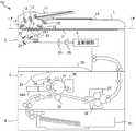
まず、図1及び図2を参照しつつ、本発明の実施の形態に係る複合機10の概略構成について説明する。なお、図1Aは前記複合機10の構成を示す正面模式図、図1Bは図1AにおけるB−B矢視図である。[First Embodiment]
[Schematic configuration of MFP 10]
First, a schematic configuration of a
図1及び図2に示すように、前記複合機10は、ADF1、画像読取部2、画像形成部3、給紙部4、主制御部5、表示入力装置6、及び通信I/F7などを備える画像形成装置である。なお、前記複合機10は、本発明に係る情報処理装置の一例である。本発明は、プリンター、ファクシミリー、コピー機、パーソナルコンピューター、タブレット端末、スマートフォン、及び携帯電話のような情報処理装置にも適用可能である。 As shown in FIGS. 1 and 2, the
前記ADF1は、図1に示すように、原稿セット部11、複数の搬送ローラー12、原稿押さえ13、及び排紙部14を備える自動原稿搬送装置である。そして、前記ADF1では、前記搬送ローラー12の各々が不図示のモーターで駆動されることにより、前記原稿セット部11に載置された原稿が前記画像読取部2による画像データの読取位置である前記原稿押さえ13の下面を通過して前記排紙部14まで搬送される。これにより、前記画像読取部2は、前記ADF1により搬送される原稿から画像データを読み取ることが可能である。 As shown in FIG. 1, the ADF 1 is an automatic document feeder that includes a
前記画像読取部2は、原稿台21、読取ユニット22、ミラー23、24、光学レンズ25、及びCCD(Charge Coupled Device)26を備える。前記原稿台21は、前記画像読取部2の上面に設けられた原稿の載置部である。前記読取ユニット22は、LED光源221及びミラー222を備え、不図示のモーターによって副走査方向(図1における左右方向)へ移動可能である。前記LED光源221は、主走査方向(図1における奥行方向)に沿って配列された多数の白色LEDを備える。前記ミラー222は、前記LED光源221から照射されて前記原稿台21上の読取位置にある原稿の表面で反射した後の光を前記ミラー23に向けて反射させる。そして、前記ミラー222で反射した光は、前記ミラー23、24によって前記光学レンズ25に導かれる。前記光学レンズ25は、入射した光を集光して前記CCD26に入射させる。前記CCD26は、前記光学レンズ25から入射される光の受光量に応じた電気信号を原稿の画像データとして前記主制御部5に入力する光電変換素子などを有する。 The
前記画像形成部3は、前記画像読取部2で読み取られた画像データ又は外部のパーソナルコンピューター等の情報処理装置から入力された画像データに基づいて画像形成処理(印刷処理)を実行する電子写真方式の画像形成部である。具体的に、前記画像形成部3は、図1に示すように、感光体ドラム31、帯電装置32、露光装置(LSU)33、現像装置34、転写ローラー35、クリーニング装置36、定着ローラー37、加圧ローラー38、及び排紙トレイ39を備える。そして、前記画像形成部3では、前記給紙部4に着脱可能な給紙カセット41から供給される用紙に以下の手順で画像が形成され、画像形成後の用紙が前記排紙トレイ39に排出される。 The
まず、前記帯電装置32によって前記感光体ドラム31が所定の電位に一様に帯電される。次に、前記露光装置33により前記感光体ドラム31の表面に画像データに基づく光が照射される。これにより、前記感光体ドラム31の表面に画像データに対応する静電潜像が形成される。そして、前記感光体ドラム31上の静電潜像は前記現像装置34によってトナー像として現像(可視像化)される。なお、前記現像装置34には、前記画像形成部3に着脱可能なトナーコンテナ34Aからトナー(現像剤)が補給される。続いて、前記感光体ドラム31に形成されたトナー像は前記転写ローラー35によって用紙に転写される。その後、用紙に転写されたトナー像は、その用紙が前記定着ローラー37及び前記加圧ローラー38の間を通過する際に前記定着ローラー37で加熱されて溶融定着する。なお、前記感光体ドラム31の表面に残存したトナーは前記クリーニング装置36で除去される。 First, the
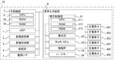
前記主制御部5は、図2に示すように、CPU51、ROM52、及びRAM53を有する。前記CPU51は、各種の演算処理を実行するプロセッサーである。前記ROM52は、前記CPU51に各種の処理を実行させるための制御プログラムなどの情報が予め記憶される不揮発性の記憶部である。前記RAM53は揮発性の記憶部であり、前記CPU51が実行する各種の処理の一時記憶メモリー(作業領域)として使用される。 The
前記通信I/F7は、前記複合機10にインターネット又はLANのような通信ネットワークを介して接続された外部装置との間でデータ通信を実行するインターフェースである。 The communication I /
[表示入力装置の構成]
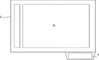
次に、図2〜図4を参照しつつ、前記表示入力装置6について説明する。なお、図4Aは、前記表示入力装置6のタッチパネル63の平面図、図4Bは、前記表示入力装置6のタッチパネル63の左側面図である。[Configuration of display input device]
Next, the
前記表示入力装置6は、図2〜図4に示すように、表示制御部61、表示部62、タッチパネル63、駆動部64、複数の圧電素子651〜656、及びハードキー66を備える。図3に示すように、前記ハードキー66は、テンキー及びスタートキーなどの各種の操作ボタンを含み、前記操作ボタンの操作信号を前記表示制御部61に入力する。 As shown in FIGS. 2 to 4, the
図2に示すように、前記表示制御部61は、CPU611、ROM612、及びRAM613を有し、前記ROM612に記憶された所定の制御プログラムを前記CPU611で実行することにより前記表示入力装置6の動作を制御する。前記RAM613は、揮発性の記憶部であって、前記CPU611が実行する各種の処理の一時記憶メモリーとして使用される。なお、前記表示制御部61は、ASIC又はDSPのような電気回路であってもよい。また、前記主制御部5が前記表示制御部61の機能を兼ねることも他の実施形態として考えられる。 As shown in FIG. 2, the
前記表示制御部61は、前記主制御部5からの制御指示に従って各種の情報を前記表示部62に表示させる。前記表示部62は、例えば液晶表示パネル又は有機ELディスプレイであり、前記表示制御部61によって制御されることにより各種の情報を表示する。前記表示部62には、各種の操作内容に対応するタッチキー及び設定画面などの各種の情報が表示される。 The
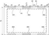
また、前記表示制御部61は、ユーザーによる前記タッチパネル63のタッチ操作及び前記ハードキー66の操作に応じて前記主制御部5に各種の情報を入力する。前記タッチパネル63は、図4Bに示すように、前記表示部62の上面に重ねて設けられている。また、前記タッチパネル63は、前記表示部62よりも外径が大きい。具体的に、前記タッチパネル63の外径は横寸法d1が240mm、縦寸法d2が149mmである。なお、図4Aに示す領域R1は、前記表示入力装置6において、前記タッチパネル63が露出している領域である。前記領域R1の外部領域は、前記表示入力装置6を操作するユーザーから見えないように前記表示入力装置6の筐体により覆われている。 The
そして、前記タッチパネル63は、ユーザーによるタッチ操作の位置を検出し、その検出した位置を前記表示制御部61に入力する。これにより、前記表示制御部61は、前記表示部62の現在の表示画面における前記タッチ操作の位置に対応する操作内容として予め設定された情報を前記主制御部5に入力することが可能である。なお、前記タッチパネル63は、例えば静電容量の変化により操作位置を検出する静電容量方式のタッチパネル、又は抵抗の変化により操作位置を検出する抵抗膜方式のタッチパネルである。 The
前記駆動部64は、前記タッチパネル63に対するユーザーのタッチ操作を検出した場合に、前記圧電素子651〜656の各々に予め定められた電圧波形の駆動信号を印加することにより前記圧電素子651〜656を振動させる。より具体的に、前記駆動部64は、同一の電圧波形の前記駆動信号を同時に前記圧電素子651〜656の各々に入力可能である。前記圧電素子651〜656の各々は、例えばPZT(チタン酸ジルコン酸鉛)のような圧電セラミックスの圧電体が一対の電極で挟まれることにより構成される。そして、前記圧電素子651〜656の各々は、前記駆動部64から印加される前記駆動信号に応じて変位することにより振動を発生させる。なお、前記駆動信号の電圧波形は、例えば正弦波、矩形波、三角波、又は鋸波などである。 When the driving
このように、前記表示入力装置6では、前記圧電素子651〜656の各々が駆動して振動することにより、前記圧電素子651〜656の各々から前記タッチパネル63に振動が伝達され、前記タッチパネル63の振動がユーザーに伝達される。従って、ユーザーは、前記タッチパネル63の操作時に前記タッチパネル63の振動により操作の感覚を得ることができる。 As described above, in the
また、図4Aに示すように、3つの前記圧電素子651〜653は、前記タッチパネル63の上端部(短手方向の一端部)において前記タッチパネル63の長手方向に予め定められた間隔で配置されている。具体的に、前記圧電素子651〜653の各々の長手方向の寸法d3は40mmである。また、前記圧電素子651の前記タッチパネル63の左端部からの離間距離d4及び前記圧電素子653の前記タッチパネル63の右端部からの離間距離d4が20mmである。さらに、前記圧電素子651〜653の配置間隔d5は40mmである。同じく、3つの前記圧電素子654〜656は、前記タッチパネル63の下端部(短手方向の一端部)において前記タッチパネル63の長手方向に予め定められた間隔で配置されている。なお、前記圧電素子651〜656の各々は、ユーザーから見えないように前記領域R1の外部領域に配置されている。また、前記圧電素子651〜653と前記圧電素子654〜656とは、それぞれが前記タッチパネル63の短手方向に対向するように配置されている。 Further, as shown in FIG. 4A, the three
なお、前記表示入力装置6では、前記タッチパネル63の長手方向に3つの前記圧電素子651〜653及び3つの前記圧電素子654〜656が配置されているが圧電素子の数はこれに限らない。即ち、前記表示入力装置6に複数の圧電素子が設けられる場合に、その圧電素子の各々に同一の駆動信号を印加させた場合でも前記タッチパネル63における振動が低減しないように前記タッチパネル63の表面及び裏面に配置すればよい。もちろん、前記圧電素子651〜656を前記タッチパネル63の表面及び裏面に配置すると共に、前記圧電素子651〜656に異なる駆動信号を印加する構成も他の実施形態として考えられる。 In the
そして、前記表示入力装置6において、前記圧電素子651〜653は、前記タッチパネル63の表面及び裏面に分けて配置されている。具体的に、前記圧電素子651〜653のうち両端の前記圧電素子651及び前記圧電素子653は前記タッチパネル63の裏面に接触して配置されている。一方、前記表示入力装置6において、前記圧電素子651〜653のうち中央の前記圧電素子652は前記タッチパネル63の表面に接触して配置されている。 In the
同じく、前記圧電素子654〜656のうち両端の前記圧電素子654及び前記圧電素子656は前記タッチパネル63の裏面に接触して配置されている。一方、前記表示入力装置6において、前記圧電素子654〜656のうち中央の前記圧電素子655は前記タッチパネル63の表面に接触して配置されている。 Similarly, the
なお、前記表示入力装置6において、前記圧電素子651、653、654、及び656が前記タッチパネル63の表面に接触して配置され、前記圧電素子652及び655が前記タッチパネル63の裏面に接触して配置されていることも考えられる。即ち、前記タッチパネル63に接触して配置される前記圧電素子651〜656のうち中央の圧電素子と左右の圧電素子とが表面及び裏面に分けて配置されていればよい。 In the
このように構成された前記表示入力装置6では、前記駆動部64により前記圧電素子651〜656に前記駆動信号が同時に入力されると、前記圧電素子651〜656の振動により前記タッチパネル63が振動する。このとき、前記圧電素子652及び前記圧電素子655により前記タッチパネル63の表面に振動が伝達され、前記圧電素子651、653、654、及び656により前記タッチパネル63の裏面に振動が伝達される。従って、前記圧電素子651、653と前記圧電素子652とにより前記タッチパネル63には逆位相の振動が与えられる。同じく、前記圧電素子654、656と前記圧電素子655とにより前記タッチパネル63には逆位相の振動が与えられる。 In the
従って、前記タッチパネル63では、前記圧電素子651〜653の振動の干渉が抑制され、特に前記タッチパネル63の中央部における振動の低減が抑制される。これにより、前記表示入力装置6は、前記タッチパネル63の前記タッチパネル63の操作時にユーザーに操作の感覚を与えることができる。また、前記表示入力装置6では、前記駆動部64が前記圧電素子651〜656の各々に同一の駆動信号を同時に印加すればよい。従って、前記表示入力装置6は、前記圧電素子651〜656の各々に位相又は周波数が異なる駆動信号を印加する必要がないため簡単な構成で実現可能である。 Therefore, in the
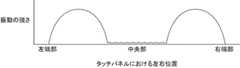
ここに、図5は、前記表示入力装置6において、前記圧電素子651〜656に同じ駆動信号が同時に印加された場合の前記タッチパネル63上の長手方向における位置と振動の強さとの関係を示す図である。図5に示すように、前記タッチパネル63では、左右両端部だけでなく中央部が振動しており、前記タッチパネル63全体においてユーザーに操作の感覚が与えられることがわかる。 FIG. 5 is a diagram showing a relationship between the position in the longitudinal direction on the
一方、図6は、前記圧電素子651〜656の全てが前記タッチパネル63の同一面(表面又は裏面)に配置されている場合に、前記圧電素子651〜656に前記駆動信号が同時に印加された場合の前記タッチパネル63上の長手方向における位置と振動の強さとの関係を示す図である。図6に示すように、前記タッチパネル63では、前記圧電素子651(654)及び前記圧電素子653(656)と前記圧電素子652(655)とにより生じる振動の干渉により中央部の振動が低減しておりユーザーに与える操作の感覚が小さいことがわかる。 On the other hand, FIG. 6 shows a case where the drive signals are simultaneously applied to the
[第2実施形態]
近年、表示部上にタッチパネルを設置したタッチパネル装置において、操作キーを押した感覚を操作者へ触感でフィードバックするフォースフィードバックと呼ばれる技術が提案されている。例えば、タッチパネルに圧電素子を設け、操作者がタッチパネルの操作面をタッチ入力した際に、圧電素子に電圧印加することで圧電素子を収縮変形させてタッチパネルを振動させ、操作者に触感をフィードバックするように構成されることがある。[Second Embodiment]
2. Description of the Related Art In recent years, a technique called force feedback has been proposed in which a touch panel device having a touch panel on a display unit feeds back a feeling of pressing an operation key to an operator with a tactile sensation. For example, when a touch panel is provided with a piezoelectric element and an operator performs touch input on the operation surface of the touch panel, voltage is applied to the piezoelectric element to cause the piezoelectric element to contract and deform to vibrate the touch panel and feed back the tactile sensation to the operator. May be configured as follows.
しかしながら、8.5inch、10.1inch等の大型タッチパネルで画面全体を振動させるには、複数個の振動デバイスを配置させて同時に駆動させる必要がある。このように、複数の振動デバイスを同時に駆動させた場合には、一つの振動デバイスの影響範囲に、隣接した振動デバイスからの影響範囲が振動干渉を起こし、タッチ入力の位置によって触感にばらつきが生じるという問題点がある。これに対し、本実施形態に係るタッチパネル装置300では、複数の振動デバイスを同時に駆動させても、触感の均一化を図ることができる。 However, in order to vibrate the entire screen with a large touch panel such as 8.5 inches or 10.1 inches, it is necessary to arrange a plurality of vibration devices and drive them simultaneously. In this way, when a plurality of vibration devices are driven simultaneously, the influence range from the adjacent vibration device causes vibration interference in the influence range of one vibration device, and the tactile sensation varies depending on the position of the touch input. There is a problem. On the other hand, in the
本実施の形態のタッチパネル装置300が搭載された画像形成装置100は、複写機であり、図7を参照すると、原稿読取部120と、原稿給送部130と、記録部140とを備えている。原稿読取部120は、記録部140の上部に配設され、原稿給送部130は、原稿読取部120の上部に配設されている。なお、本件の画像形成装置100は、複写機で説明するが、スキャナー、複合機等が含まれる。 The
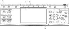
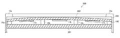
画像形成装置100の前面側には、画像形成装置100の設定や動作指示を行うタッチパネル装置300が配設されている。タッチパネル装置300は、図8及び図9を参照すると、操作入力を受け付ける各種操作キーを表示する表示部301と、表示部301の表示面に設けられ、操作者の指先やスタイラス等の押圧によるタッチ入力を検知し、タッチ入力が検知された位置に対応する信号を出力することで、表示部301に表示された操作キーへの操作を受け付けるタッチパネル302とを備えている。表示部301及びタッチパネル302は、略同一の形状を有する、短辺が縦方向に、長辺が横方向に配置された長方形である。表示部301としては、例えば液晶表示パネルが用いることができる。また、タッチパネル302としては、例えば抵抗膜方式や静電容量方式等を用いることができる。 On the front side of the
表示部301は、図9を参照すると、筐体303内に収納保持され、筐体303には、表示部301及びタッチパネル302の周辺領域を覆うアッパカバー13aが設けられている。表示部301上には、アッパカバー13aで覆われた箇所に設けられた複数の弾性部材14a〜14hを介して、タッチパネル302が保持されている。弾性部材14a〜14hは、ゴム等の樹脂で構成され、弾性部材14a〜14hの上面は、タッチパネル302を固定する固定面となる。弾性部材14a〜14hの上面に塗布された粘着材によってタッチパネル302が固定される。本実施の形態では、弾性部材14a〜14dと、弾性部材14e〜14hとが短辺方向にそれぞれ対向してアッパカバー13aで覆われた箇所に配置されている。 Referring to FIG. 9, the
弾性部材14a〜14hの高さ、すなわち表示部301から弾性部材14a〜14hの固定面までの高さは、2段階以上の異なる高さに設定されている。本実施の形態では、2段階の異なる高さに設定されており、弾性部材14a、14d、14e、14hよりも弾性部材14b、14c、14f、14gが高く設定されている。これにより、タッチパネル302は、長辺方向の中央部分が上方に湾曲して固定されている。 The heights of the
また、アッパカバー13aで覆われた箇所のタッチパネル302の裏面には、圧電素子17a〜17fが貼着されている。圧電素子17は、タッチパネル302を振動させる振動部として機能する。本実施の形態では、圧電素子17a〜17cと、圧電素子17d〜17fとが短辺方向にそれぞれ対向してアッパカバー13aで覆われた箇所に配置されている。 In addition,
タッチパネル装置300には、図8を参照すると、印刷枚数等の数値を入力するためのテンキー、設定情報を初期化させる指示を入力するためのリセットキー、複写動作を停止させたり、入力された数値を消去させたりするためのストップキー、印刷動作を開始させる出力指示を入力するためのスタートキー等の常設操作キーと共に、画像形成装置100の状態や各種操作画面が表示される表示領域19とが設けられている。 Referring to FIG. 8, the
原稿読取部120は、図7を参照すると、スキャナー121と、プラテンガラス122と、原稿読取スリット123とを備える。スキャナー121は、露光ランプ及びCCD(Charge Coupled Device)センサー等から構成され、原稿給送部130による原稿MSの搬送方向に移動可能に構成されている。プラテンガラス122は、ガラス等の透明部材により構成された原稿台である。原稿読取スリット123は、原稿給送部130による原稿MSの搬送方向と直交方向に形成されたスリットを有する。 As shown in FIG. 7, the
プラテンガラス122に載置された原稿MSを読み取る場合には、スキャナー121は、プラテンガラス122に対向する位置に移動され、プラテンガラス122に載置された原稿MSを走査しながら原稿MSを読み取って画像データを取得し、取得した画像データを記録部140に出力する。また、原稿給送部130により搬送された原稿MSを読み取る場合には、スキャナー121は、原稿読取スリット123と対向する位置に移動され、原稿読取スリット123を介し、原稿給送部130による原稿MSの搬送動作と同期して原稿MSを読み取って画像データを取得し、取得した画像データを記録部140に出力する。 When reading the document MS placed on the
原稿給送部130は、原稿載置部131と、原稿排出部132と、原稿搬送機構133とを備えている。原稿載置部131に載置された原稿MSは、原稿搬送機構133によって、1枚ずつ順に繰り出されて、原稿読取部120の原稿読取スリット123に対向する位置へ搬送され、その後、原稿排出部132に排出される。なお、原稿給送部130は、可倒式に構成され、原稿給送部130を上方に持ち上げることで、プラテンガラス122の上面を開放させることができる。 The
記録部140は、画像形成部150を備えると共に、給紙部160と、搬送路170と、搬送ローラー181と、排出ローラー182と、排出トレイ190とを備えている。 The
給紙部160は、記録紙Pを収納する複数の給紙カセット161a〜161dと、給紙カセット161a〜161dから記録紙Pを1枚ずつ搬送路170に繰り出す給紙ローラー162とを備えている。給紙ローラー162、搬送ローラー181及び排出ローラー182が搬送部として機能し、記録紙Pが搬送される。給紙ローラー162によって搬送路170に繰り出された記録紙Pは、搬送ローラー181によって画像形成部150に搬送される。そして、画像形成部150によって記録が施された記録紙Pは、排出ローラー182によって機外に出力される。記録が施された記録紙Pは、排出ローラー182に導かれ、排出トレイ190に出力される。 The
画像形成部150は、感光体ドラム151と、帯電部152、露光部153と、現像部154と、転写部155と、クリーニング部156と、定着部157とを備えている。露光部153は、レーザー装置やミラー等を備えた光学ユニットであり、画像データに基づいてレーザー光を出力して、帯電部152によって帯電された感光体ドラム151を露光し、感光体ドラム151の表面に静電潜像を形成する。現像部154は、トナーを用いて感光体ドラム151に形成された静電潜像を現像する現像ユニットであり、静電潜像に基づいたトナー像を感光体ドラム151上に形成させる。転写部155は、現像部154によって感光体ドラム151上に形成されたトナー像を記録紙Pに転写させる。定着部157は、転写部155によってトナー像が転写された記録紙Pを加熱してトナー像を記録紙Pに定着させる。 The
次に、画像形成装置100のハードウェア構成例について図10を参照して説明する。 Next, a hardware configuration example of the
画像形成装置100のタッチパネル装置300、原稿読取部120、原稿給送部130、画像形成部150及び搬送部(給紙ローラー162、搬送ローラー181、排出ローラー182)は、制御部200に接続され、制御部200によって動作制御される。また、制御部200には、記憶部171と、画像処理部172とが接続されている。 The
制御部200は、ROM(Read Only Memory)、RAM(Random Access Memory)等を備えたマイクロコンピュータ等の情報処理部である。ROMには画像形成装置100の動作制御を行うための制御プログラムが記憶されている。制御部200は、ROMに記憶されている制御プログラムを読み出し、制御プログラムをRAMに展開させることで、タッチパネル装置300から入力された所定の指示情報等に応じて装置全体の制御を行う。 The
記憶部171は、半導体メモリやHDD(Hard Disk Drive)等の記憶部であり、原稿読取部120によって原稿を読み取ることで取得された画像データが記憶される。 The
画像処理部172は、画像データに対して所定の画像処理を行う。例えば、画像処理部172は、拡大縮小処理、濃度調整、又は階調調整等の画像改善処理を行う。 The
タッチパネル装置300には、図10を参照すると、圧電素子に予め定められた電圧波形の駆動信号を1又は複数回入力して前記圧電素子の短辺方向に対向配置された圧電素子17aと圧電素子17dとからなる圧電素子対を駆動する第1振動駆動部21aと、短辺方向に対向配置された圧電素子17bと圧電素子17eとからなる圧電素子対を駆動する第2振動駆動部21b、短辺方向に対向配置された圧電素子17cと圧電素子17fとからなる圧電素子対を駆動する第3振動駆動部21cとが設けられている。振動駆動部21a〜21cは、タッチパネル302へのタッチ入力に対して、制御部200の制御に基づいて圧電素子17a〜17fに予め定められた同一の電圧波形の駆動信号を1又は複数回入力してタッチパネル302を振動させる。 Referring to FIG. 10, the
タッチパネル302がフラットである場合には、振動駆動部21a〜21cによって圧電素子17a〜17fに全て同一の振動を発生させると、振動が均一に伝わってくるため、中央部等では振動波同士が干渉により打ち消しあい、振動が相殺されてしまう。これに対し、本実施の形態のタッチパネル302は、弾性部材14a〜14hの高さを2段階に変えて、タッチパネル302を長辺方向の中央部分が上方に湾曲するように構成されている。これにより、振動波の伝搬に変化が発生するため、干渉による打ち消しを低減することができ、触感の均一化を図ることができるという効果を奏する。 In the case where the
なお、本実施の形態では、弾性部材14a〜14hの高さを2段階に変えて、タッチパネル302を長辺方向の中央部分が上方に湾曲するように構成したが、弾性部材、すなわち固定面の数や、高さの段階数は適宜設定することができる。例えば、凹凸をつけて波打つようにタッチパネル302を湾曲させたり、弾性部材14a〜hの高さを不規則に変えてさらに複雑にタッチパネル302を湾曲させたりしても良い。 In the present embodiment, the height of the
なお、本発明が上記各実施の形態に限定されず、本発明の技術思想の範囲内において、各実施の形態は適宜変更され得ることは明らかである。また、上記構成部材の数、位置、形状等は上記実施の形態に限定されず、本発明を実施する上で好適な数、位置、形状等にすることができる。 Note that the present invention is not limited to the above-described embodiments, and it is obvious that the embodiments can be appropriately changed within the scope of the technical idea of the present invention. In addition, the number, position, shape, and the like of the constituent members are not limited to the above-described embodiment, and can be set to a number, position, shape, and the like that are suitable for implementing the present invention.
Claims (7)
Translated fromJapanese前記表示部の上面に設けられ、タッチ操作の位置を検出するタッチパネルと、
前記タッチパネルの表面及び裏面に分けて配置された複数の圧電素子と、
前記タッチパネルのタッチ操作に応じて前記圧電素子を駆動して前記タッチパネルを振動させる駆動部と、
を備える表示入力装置。A display unit;
A touch panel provided on an upper surface of the display unit and detecting a position of a touch operation;
A plurality of piezoelectric elements arranged separately on the front and back surfaces of the touch panel;
A drive unit that vibrates the touch panel by driving the piezoelectric element in response to a touch operation of the touch panel;
A display input device comprising:
3つの前記圧電素子のうち中央の前記圧電素子と両端の前記圧電素子とが前記タッチパネルの表面及び裏面に分けて配置された請求項1に記載の表示入力装置。A plurality of the piezoelectric elements includes three piezoelectric elements arranged at predetermined intervals in the longitudinal direction of the touch panel,
The display input device according to claim 1, wherein among the three piezoelectric elements, the central piezoelectric element and the piezoelectric elements at both ends are arranged separately on a front surface and a back surface of the touch panel.
該表示部の上面に設けられた複数の弾性部材と、
複数の前記弾性部材の上面に固定されたタッチパネルと、
前記タッチパネルを振動させる複数の圧電素子とを備え、
複数の前記弾性部材の上面は、2段階以上の複数の高さに設定され、前記タッチパネルは、湾曲された状態で固定されているタッチパネル装置。A display for displaying a screen;
A plurality of elastic members provided on the upper surface of the display unit;
A touch panel fixed to the upper surfaces of the plurality of elastic members;
A plurality of piezoelectric elements that vibrate the touch panel;
The upper surfaces of the plurality of elastic members are set to a plurality of heights of two or more stages, and the touch panel is fixed in a curved state.
Applications Claiming Priority (5)
| Application Number | Priority Date | Filing Date | Title |
|---|---|---|---|
| JP2013114477 | 2013-05-30 | ||
| JP2013114477 | 2013-05-30 | ||
| JP2013115148 | 2013-05-31 | ||
| JP2013115148 | 2013-05-31 | ||
| PCT/JP2014/064096WO2014192801A1 (en) | 2013-05-30 | 2014-05-28 | Display/input apparatus, information processing apparatus, and touch panel apparatus |
Publications (2)
| Publication Number | Publication Date |
|---|---|
| JP5976212B2 JP5976212B2 (en) | 2016-08-23 |
| JPWO2014192801A1true JPWO2014192801A1 (en) | 2017-02-23 |
Family
ID=51988826
Family Applications (1)
| Application Number | Title | Priority Date | Filing Date |
|---|---|---|---|
| JP2015519898AExpired - Fee RelatedJP5976212B2 (en) | 2013-05-30 | 2014-05-28 | Display input device, information processing device, touch panel device |
Country Status (4)
| Country | Link |
|---|---|
| US (1) | US10088904B2 (en) |
| JP (1) | JP5976212B2 (en) |
| CN (1) | CN105393195B (en) |
| WO (1) | WO2014192801A1 (en) |
Families Citing this family (2)
| Publication number | Priority date | Publication date | Assignee | Title |
|---|---|---|---|---|
| JP6222186B2 (en)* | 2015-08-11 | 2017-11-01 | コニカミノルタ株式会社 | Operation panel and image forming apparatus having the same |
| JP7649108B2 (en)* | 2020-03-11 | 2025-03-19 | Tdk株式会社 | Vibration Device |
Citations (6)
| Publication number | Priority date | Publication date | Assignee | Title |
|---|---|---|---|---|
| JP2002149312A (en)* | 2000-08-08 | 2002-05-24 | Ntt Docomo Inc | Portable electronic device, electronic device, vibration generator, notification method by vibration, and notification control method |
| US20060022952A1 (en)* | 2004-07-07 | 2006-02-02 | Matti Ryynanen | Electrostrictive polymer as a combined haptic-seal actuator |
| JP2008516348A (en)* | 2004-10-08 | 2008-05-15 | イマージョン コーポレーション | Haptic feedback for simulating buttons and scrolling motion on touch input devices |
| JP2011043925A (en)* | 2009-08-19 | 2011-03-03 | Nissha Printing Co Ltd | Flexurally vibrating actuator and touch panel with tactile sensation feedback function using the same |
| WO2012053202A1 (en)* | 2010-10-21 | 2012-04-26 | 京セラ株式会社 | Touch panel device |
| JP2013033458A (en)* | 2011-07-06 | 2013-02-14 | Panasonic Corp | Electronic device |
Family Cites Families (11)
| Publication number | Priority date | Publication date | Assignee | Title |
|---|---|---|---|---|
| JP5208362B2 (en)* | 2005-10-28 | 2013-06-12 | ソニー株式会社 | Electronics |
| US20100117809A1 (en)* | 2008-11-11 | 2010-05-13 | Motorola Inc. | Display module with piezoelectric haptics |
| TW201101137A (en)* | 2009-06-29 | 2011-01-01 | J Touch Corp | Touch panel with matrix type tactile feedback |
| US8310457B2 (en)* | 2009-06-30 | 2012-11-13 | Research In Motion Limited | Portable electronic device including tactile touch-sensitive input device and method of protecting same |
| US20100328229A1 (en)* | 2009-06-30 | 2010-12-30 | Research In Motion Limited | Method and apparatus for providing tactile feedback |
| US8378797B2 (en)* | 2009-07-17 | 2013-02-19 | Apple Inc. | Method and apparatus for localization of haptic feedback |
| EP2472365B1 (en)* | 2009-08-27 | 2016-10-12 | Kyocera Corporation | Tactile sensation imparting device and control method of tactile sensation imparting device |
| JP2011175364A (en) | 2010-02-23 | 2011-09-08 | Kyocera Corp | Method for driving touch panel device |
| JP5588016B2 (en)* | 2010-11-11 | 2014-09-10 | 京セラ株式会社 | Input device and control method of input device |
| CN202582565U (en)* | 2012-01-21 | 2012-12-05 | 汉王科技股份有限公司 | A piezoelectric sensor, and a touch-controlled assembly and a mobile terminal which utilize the piezoelectric sensor |
| KR20140043198A (en)* | 2012-09-28 | 2014-04-08 | 삼성디스플레이 주식회사 | Curved display apparatus |
- 2014
- 2014-05-28USUS14/894,948patent/US10088904B2/enactiveActive
- 2014-05-28WOPCT/JP2014/064096patent/WO2014192801A1/enactiveApplication Filing
- 2014-05-28JPJP2015519898Apatent/JP5976212B2/ennot_activeExpired - Fee Related
- 2014-05-28CNCN201480030608.7Apatent/CN105393195B/ennot_activeExpired - Fee Related
Patent Citations (6)
| Publication number | Priority date | Publication date | Assignee | Title |
|---|---|---|---|---|
| JP2002149312A (en)* | 2000-08-08 | 2002-05-24 | Ntt Docomo Inc | Portable electronic device, electronic device, vibration generator, notification method by vibration, and notification control method |
| US20060022952A1 (en)* | 2004-07-07 | 2006-02-02 | Matti Ryynanen | Electrostrictive polymer as a combined haptic-seal actuator |
| JP2008516348A (en)* | 2004-10-08 | 2008-05-15 | イマージョン コーポレーション | Haptic feedback for simulating buttons and scrolling motion on touch input devices |
| JP2011043925A (en)* | 2009-08-19 | 2011-03-03 | Nissha Printing Co Ltd | Flexurally vibrating actuator and touch panel with tactile sensation feedback function using the same |
| WO2012053202A1 (en)* | 2010-10-21 | 2012-04-26 | 京セラ株式会社 | Touch panel device |
| JP2013033458A (en)* | 2011-07-06 | 2013-02-14 | Panasonic Corp | Electronic device |
Also Published As
| Publication number | Publication date |
|---|---|
| US10088904B2 (en) | 2018-10-02 |
| JP5976212B2 (en) | 2016-08-23 |
| US20160103490A1 (en) | 2016-04-14 |
| CN105393195B (en) | 2018-09-25 |
| WO2014192801A1 (en) | 2014-12-04 |
| CN105393195A (en) | 2016-03-09 |
Similar Documents
| Publication | Publication Date | Title |
|---|---|---|
| JP5972253B2 (en) | Display input device, information processing device | |
| KR101678287B1 (en) | Touch panel apparatus and electronic apparatus provided with same | |
| JP6062573B2 (en) | Touch panel device and touch panel control method | |
| JP5849061B2 (en) | Display input device and image forming apparatus having the same | |
| CN103685807B (en) | Display input device and image processing system | |
| CN103914137A (en) | Operation input device, and information processing apparatus provided with the same | |
| US9329687B2 (en) | Touch panel device having vibration function | |
| JP2015162152A (en) | Touch panel device and image forming apparatus | |
| JP5976212B2 (en) | Display input device, information processing device, touch panel device | |
| JP2012178103A (en) | Input device and image forming apparatus | |
| JP5934277B2 (en) | Operating device and positional deviation adjusting method | |
| JP2015162153A (en) | Touch panel device and image forming apparatus | |
| JP2015125720A (en) | Operating device and operating method | |
| JP5996515B2 (en) | Operation panel device and image forming apparatus | |
| JP2015104835A (en) | Operation panel device and image forming apparatus | |
| JP2015106231A (en) | Operation panel device and image forming apparatus | |
| JP2016033727A (en) | Touch panel device and image forming apparatus including touch panel device |
Legal Events
| Date | Code | Title | Description |
|---|---|---|---|
| TRDD | Decision of grant or rejection written | ||
| A01 | Written decision to grant a patent or to grant a registration (utility model) | Free format text:JAPANESE INTERMEDIATE CODE: A01 Effective date:20160621 | |
| A61 | First payment of annual fees (during grant procedure) | Free format text:JAPANESE INTERMEDIATE CODE: A61 Effective date:20160719 | |
| R150 | Certificate of patent or registration of utility model | Ref document number:5976212 Country of ref document:JP Free format text:JAPANESE INTERMEDIATE CODE: R150 | |
| LAPS | Cancellation because of no payment of annual fees |