JPWO2013128565A1 - Lighting correction device - Google Patents
Lighting correction deviceDownload PDFInfo
- Publication number
- JPWO2013128565A1 JPWO2013128565A1JP2014501869AJP2014501869AJPWO2013128565A1JP WO2013128565 A1JPWO2013128565 A1JP WO2013128565A1JP 2014501869 AJP2014501869 AJP 2014501869AJP 2014501869 AJP2014501869 AJP 2014501869AJP WO2013128565 A1JPWO2013128565 A1JP WO2013128565A1
- Authority
- JP
- Japan
- Prior art keywords
- luminance
- organic
- panel
- light
- correction
- Prior art date
- Legal status (The legal status is an assumption and is not a legal conclusion. Google has not performed a legal analysis and makes no representation as to the accuracy of the status listed.)
- Pending
Links
Images


Landscapes
- Electroluminescent Light Sources (AREA)
- Circuit Arrangement For Electric Light Sources In General (AREA)
- Devices For Indicating Variable Information By Combining Individual Elements (AREA)
Abstract
Translated fromJapaneseDescription
Translated fromJapanese本発明は、面発光する照明装置に対して、照明の均一性を得るために照明装置への出力値を補正する照明補正装置に関する。 The present invention relates to an illumination correction device that corrects an output value to an illumination device in order to obtain illumination uniformity for an illumination device that emits light from a surface.
近年、一部の携帯型機器などのフラットパネルディスプレイ(FPD)では、面発光する発光素子として、有機EL(electroluminescence)素子が用いられることが多くなっている。 In recent years, in some flat panel displays (FPD) such as portable devices, organic EL (electroluminescence) elements are often used as light emitting elements that emit light.
この有機EL素子は直流の低電圧により駆動されることで高い発光効率を有し、軽量かつ薄型化が可能であると共に、ほとんど発熱がないという特質を有している。 This organic EL element has high light emission efficiency when driven by a DC low voltage, and can be reduced in weight and thickness, and has the property that it hardly generates heat.
また、有機EL素子はEL発光層に用いる素材の選択により、R(赤)、G(緑)、B(青)やその他の発光色を得ることができ、この各発光色を単独で、または二種以上の発光色を組み合わせることにより、白色もしくはこれに近い発光色を得ることも可能となる。そこで、有機EL素子を面発光源として有機EL照明装置として構成することで、例えば装飾用の光源や、室内等を照明する高効率な光源としての普及が期待されている。 In addition, the organic EL element can obtain R (red), G (green), B (blue) and other emission colors by selecting a material used for the EL emission layer, and each of these emission colors can be used alone or By combining two or more kinds of emission colors, it becomes possible to obtain white or an emission color close to this. Accordingly, by configuring the organic EL element as an organic EL lighting device using the organic EL element as a surface light source, it is expected to spread as, for example, a decorative light source or a highly efficient light source for illuminating a room or the like.
例えば、特許文献1には、透明の基板上に透明電極、面発光源である有機EL素子を有する有機発光層、背面電極が順次積層された有機EL照明装置が提案されている。 For example,
また、特許文献2には、製造の不均一により発生する液晶パネルの補正データを生成する画像補正データ生成方法が提案されている。 Patent Document 2 proposes an image correction data generation method for generating correction data for a liquid crystal panel generated due to non-uniform manufacturing.
特許文献1に記載の有機EL照明装置では、面発光源である有機EL素子が均一な輝度を持つことを前提に、有機ELパネル全体に対して背面電極を正極、透明電極を負極として駆動電圧が印加されるようになっている。 In the organic EL lighting device described in
しかしながら、有機ELパネル全体で制御するので、有機ELパネルの中央部と端部とでは、送電する際の抵抗等の影響により、輝度が不均一となる場合がある。 However, since the control is performed for the entire organic EL panel, the luminance may be nonuniform at the center and the end of the organic EL panel due to the influence of resistance or the like when transmitting power.
特許文献2に記載の画像補正データ生成方法では、画素単位で制御する液晶パネルを対象に、各画素の製造の不均一により発生する表示むらを抑制するため、出力画像データに対してバンドパスフィルタリングを行うものである。しかしながら、画素単位で制御する液晶パネルを前提とした技術を、有機ELパネル全体で制御する有機EL照明装置には適用することができなかった。 In the image correction data generation method described in Patent Literature 2, bandpass filtering is performed on output image data for a liquid crystal panel controlled in units of pixels in order to suppress display unevenness caused by non-uniform manufacturing of each pixel. Is to do. However, the technology based on the liquid crystal panel that is controlled in pixel units cannot be applied to the organic EL lighting device that controls the entire organic EL panel.
本発明は、このような課題に鑑みてなされたものであり、有機EL照明装置において、輝度が均一になるように発光させる照明補正装置を提案することを目的とする。 The present invention has been made in view of such problems, and an object of the present invention is to propose an illumination correction apparatus that emits light so that the luminance is uniform in an organic EL lighting apparatus.
前記目的を達成するため、本発明に係る照明補正装置の第1の特徴は、面発光する複数のブロックで配列された発光層を有する発光パネルと、カメラにより前記発光パネルが撮像された撮像データに基づいて生成された補正データを記憶する記憶部と、前記補正データに基づいて、前記複数のブロック間の輝度が均一になるように、前記ブロックごとに前記発光パネルを発光させる制御設定値を決定する決定部と、を備えたことにある。 In order to achieve the above object, a first feature of the illumination correction apparatus according to the present invention is a light emitting panel having a light emitting layer arranged in a plurality of blocks that emit surface light, and imaging data in which the light emitting panel is imaged by a camera. And a control setting value for causing the light-emitting panel to emit light for each block so that the luminance between the plurality of blocks is uniform based on the correction data. And a determination unit for determining.
また、本発明に係る照明補正装置の第2の特徴は、輝度の基準となる複数のブロックで配列された発光層を有する基準発光パネルを前記カメラで撮像した撮像データに基づいて、前記基準発光パネルが有する発光層のブロックごとの輝度を基準輝度として算出する基準輝度算出部と、前記発光パネルを前記カメラで撮像した撮像データに基づいて、前記発光パネルが有する発光層のブロックごとの輝度を補正対象輝度として算出する輝度算出部と、前記基準輝度に基づいて、前記補正対象輝度を補正するための前記補正データを生成し、前記記憶部に記憶させる補正データ生成部と、を備えたことにある。 A second feature of the illumination correction apparatus according to the present invention is that the reference light emission is based on image data obtained by imaging a reference light-emitting panel having a light-emitting layer arranged in a plurality of blocks serving as a reference for luminance with the camera. Based on imaging data obtained by imaging the light emitting panel with the camera, the luminance for each block of the light emitting layer of the light emitting panel is calculated based on the reference luminance calculating unit that calculates the luminance of each block of the light emitting layer of the panel as the reference luminance. A luminance calculation unit that calculates the correction target luminance; and a correction data generation unit that generates the correction data for correcting the correction target luminance based on the reference luminance and stores the correction data in the storage unit. It is in.
また、本発明に係る照明補正装置の第3の特徴は、前記発光層は、自発光素子を用いて成形されていることにある。 A third feature of the illumination correction apparatus according to the present invention is that the light emitting layer is formed using a self light emitting element.
また、本発明に係る照明補正装置の第4の特徴は、前記発光層は、有機EL素子を用いて成形されていることにある。 Moreover, the 4th characteristic of the illumination correction apparatus which concerns on this invention exists in the said light emitting layer being shape | molded using the organic EL element.
また、本発明に係る照明補正装置の第5の特徴は、前記発光パネルと前記基準発光パネルとは、同一の立体形状を有することにある。 A fifth feature of the illumination correction apparatus according to the present invention is that the light emitting panel and the reference light emitting panel have the same three-dimensional shape.
本発明の照明補正装置によれば、有機EL照明装置において、輝度が均一になるように発光させることができる。 According to the illumination correction apparatus of the present invention, the organic EL illumination apparatus can emit light with uniform luminance.
(実施形態1)
以下、本発明に係る照明補正装置の実施形態1について説明する。(Embodiment 1)
<構成の説明>
図1は、本発明の実施形態1に係る照明補正装置を含む照明補正システムの全体構成図を示す図である。<Description of configuration>
FIG. 1 is a diagram showing an overall configuration diagram of an illumination correction system including an illumination correction apparatus according to
図1に示すように、この照明補正システム100は、照明補正装置1と、演算処理装置2と、カメラ3とを備えている。 As shown in FIG. 1, the
照明補正装置1は、制御部10と、有機ELパネル20を有し、制御部10からの制御信号により有機ELパネル20を発光させる装置である。 The
有機ELパネル20は、透明電極31、有機発光層32と、背面電極33とが順次積層させている。有機発光層32は、面発光する有機EL(electroluminescence)素子を用いて、9つの領域に分割して、ブロック21〜29で配列されている。後述するが、このブロック21〜29間の輝度が均一になるように補正されて、有機発光層32が発光される。 In the
カメラ3は、所定位置に固定された固定式の撮像装置であり、照明補正装置1を撮像し、撮像した画像データを演算処理装置2へ供給する。 The
演算処理装置2は、カメラ3により撮像された画像データに基づいて、ブロック21〜29間の輝度を均一にするための補正データを生成する。 The arithmetic processing device 2 generates correction data for making the luminance between the
図2は、本発明の実施形態1に係る照明補正装置1を含む照明補正システム100の機能構成を示す図である。 FIG. 2 is a diagram illustrating a functional configuration of the
図2に示すように、照明補正システム100は、照明補正装置1と、演算処理装置2と、カメラ3とを備えている。そのうち、演算処理装置2と、カメラ3との構成については、上述したので、説明を省略する。 As shown in FIG. 2, the
照明補正装置1は、制御部10と、有機ELパネル20と、電源回路41と、調光入力部42とを備えている。 The
有機ELパネル20は、上述したように、面発光する9つのブロック21〜29で配列された有機発光層32を有している。この有機発光層32を表裏から挟むように、透明電極31及び背面電極33とが設けられており、有機発光層32のブロック21〜29それぞれに対応する透明電極31及び背面電極33が印加されることにより、有機発光層32のブロック21〜29それぞれが発光する。 As described above, the
電源回路41は、制御部10や、制御部10を介して有機ELパネル20へ電圧を印加する。 The
調光入力部42は、ユーザ操作により、有機ELパネル20の調光ボリュームの設定を行う。例えば、調光入力部42は、スライド式のスイッチを有し、このスイッチのスライド量の応じた調光ボリュームを制御部10へ供給する。 The
制御部10は、記憶制御部11と、メモリ12と、調光回路13とを備える。 The
記憶制御部11は、カメラ3により有機ELパネル20が撮像された撮像データに基づいて演算処理装置2により生成された補正データをメモリ12に記憶させる。この補正データは、9つのブロック21〜29間の輝度が均一になるように演算処理装置2により生成され、照明補正装置1へ供給されたものである。 The
メモリ12は、例えば、不揮発性半導体等で構成され、記憶制御部11の指示により、演算処理装置2により生成された補正データを記憶する。具体的には、メモリ12は、ブロック21〜29毎に、電流値及び電圧値それぞれの補正データを記憶している。 The
調光回路13は、補正データに基づいて、9つのブロック21〜29間の輝度が均一になるように、9つのブロック21〜29毎に有機ELパネル20を発光させる制御設定値を決定する。例えば、調光回路13は、メモリ12に記憶された補正データに基づいて、9つのブロック21〜29間の輝度が均一になるように、9つのブロック21〜29毎に、制御設定値として、有機ELパネル20へ印加させる電圧値及び電流値を決定する。 Based on the correction data, the
そして、調光回路13は、決定された制御設定値に基づいて、有機発光層32のブロック21〜29それぞれに対応する透明電極31及び背面電極33に、電流及び電圧を印加する。 And the
<動作の説明>
次に、本発明の実施形態1に係る照明補正装置1の動作について説明する。<Description of operation>
Next, operation | movement of the
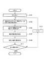
図3は、本発明の実施形態1に係る照明補正装置1において、電源のスイッチが押下操作された際の処理手順を示したフローチャートである。 FIG. 3 is a flowchart showing a processing procedure when the power switch is pressed in the
図3に示すように、照明補正装置1の制御部10の調光回路13は、カウンタの値に初期値として、“1”を代入する(ステップS101)。 As illustrated in FIG. 3, the dimming
次に、調光回路13は、n番目のブロックについて、調光ボリュームに比例した電流値及び電圧値を算出する(ステップS103)。具体的には、調光回路13は、調光入力部42から、ユーザ操作に基づいて供給された調光ボリュームに比例した電流値及び電圧値を算出する。なお、ここでは、9つのブロックは、ブロック21〜29の順に割り付けられているとする。 Next, the dimming
そして、調光回路13は、メモリ12からn番目のブロックの補正データを読み込む(ステップS105)。 Then, the dimming
次に、調光回路13は、最終の電流値及び電圧値を決定する(ステップS107)。具体的には、ステップS103において算出されたn番目のブロックの電流値及び電圧値に、それぞれステップS105において読み込んだn番目のブロックの補正データを加算することにより最終の電流値及び電圧値を制御設定値として決定する。 Next, the dimming
そして、決定された最終の電流値及び電圧値に基づいて、n番目のブロック目に電流・電圧を印加する(ステップS109)。具体的には、調光回路13は、有機発光層32のn番目のブロック目に対応する透明電極31及び背面電極33に、電流・電圧を印加する。 Then, based on the determined final current value and voltage value, a current / voltage is applied to the nth block (step S109). Specifically, the
次に、調光回路13は、全ての調光が終了したか否かを判定する(ステップS111)。具体的には、調光回路13は、9つのブロック21〜29に対して調光が完了したか否かを判定する。 Next, the dimming
ステップS111において、全ての調光が終了していないと判定された場合(NOの場合)、調光回路13は、カウンタnの値に、“1”だけ加算する(ステップS113)。 If it is determined in step S111 that all dimming has not been completed (NO), the dimming
このように、調光回路13は、ブロック21〜29に応じて電流・電圧を印加することができる。 Thus, the dimming
以上のように、本発明の実施形態1に係る照明補正装置1によれば、面発光する複数のブロックで配列された有機発光層32を有する有機ELパネル20と、カメラ3により有機ELパネル20が撮像された撮像データに基づいて生成された補正データを記憶するメモリ12と、補正データに基づいて、複数のブロック間の輝度が均一になるように、ブロックごとに有機パネルを発光させるための制御設定値を決定する調光回路13とを備えるので、有機ELパネル20のブロック21〜29間において輝度が均一になるように発光させることができる。 As described above, according to the
(実施形態2)
以下、本発明に係る照明補正装置の実施形態2について説明する。(Embodiment 2)
Hereinafter, a second embodiment of the illumination correction apparatus according to the present invention will be described.
<構成の説明>
図4は、本発明の実施形態2に係る照明補正装置を含む照明補正システムの全体構成図を示す図である。<Description of configuration>
FIG. 4 is a diagram showing an overall configuration diagram of an illumination correction system including an illumination correction apparatus according to Embodiment 2 of the present invention.
図4に示すように、この照明補正システム100は、照明補正装置1Aと、演算処理装置2と、カメラ3とを備えている。このうち、演算処理装置2と、カメラ3とについては、本発明の実施形態1に係る照明補正装置1が備える同一符号が付された構成と同一であるので、説明を省略する。 As shown in FIG. 4, the
照明補正装置1Aは、制御部10Aと、有機ELパネル20Aを有し、制御部10Aからの制御信号により有機ELパネル20Aを発光させる装置である。 The
有機ELパネル20Aは、透明電極31、有機発光層32と、背面電極33とを順次積層させている。有機発光層32は、面発光する有機EL(electroluminescence)素子を用いて、9つの領域に分割して、ブロック21〜29で配列されている。後述するが、このブロック21〜29間の輝度が均一になるように補正されて、有機発光層32が発光される。 In the
また、有機ELパネル20Aは、立体形状を有している。具体的には、上下方向の中央部からカメラ3までの距離が相対的に短く、上下端部からカメラ3までの距離が相対的に長くなるように湾曲している。 The
この有機ELパネル20Aのように、立体形状を有している場合、観測者からの距離や観測者の見る角度などによって、ブロック毎に輝度が異なる場合がある。 In the case where the
そこで、本発明の実施形態2に係る照明補正装置1Aでは、有機ELパネル20Aと同一形状を有する、予め均一な輝度となるように調整された有機ELパネル20B(図示しない)をカメラ3で撮像した撮像データに基づいて、有機ELパネル20Aを調光する。 Therefore, in the
図5は、本発明の実施形態4に係る照明補正装置1Aを含む照明補正システム100の機能構成を示す図である。 FIG. 5 is a diagram showing a functional configuration of an
図5に示すように、照明補正システム100は、照明補正装置1Aと、演算処理装置2と、カメラ3とを備えている。そのうち、演算処理装置2と、カメラ3とについては、上述したので、説明を省略する。 As shown in FIG. 5, the
照明補正装置1Aは、制御部10Aと、有機ELパネル20Aと、電源回路41と、調光入力部42とを備える。これらの構成のうち、電源回路41と、調光入力部42とについては、本発明の実施形態1に係る照明補正装置1が備える同一符号が付された構成と同一であるので、説明を省略する。 The
有機ELパネル20Aは、上述したように、面発光する9つのブロック21〜29で配列された有機発光層32を有している。有機発光層32は、上下方向の中央部からカメラ3までの距離が相対的に短く、上下端部からカメラ3までの距離が相対的に長くなるように湾曲している。 As described above, the
制御部10Aは、基準輝度算出部15と、輝度算出部16と、補正データ生成部17と、メモリ12と、調光回路13とを備える。 The
基準輝度算出部15は、面発光する9つのブロック21〜29で配列された有機発光層32を有する有機ELパネル20Bをカメラ3で撮像した撮像データに基づいて、有機ELパネル20Bが有する有機発光層32の9つのブロック21〜29ごとの輝度を基準輝度として算出する。 The reference
輝度算出部16は、有機ELパネル20Aをカメラ3で撮像した撮像データに基づいて、有機ELパネル20Aが有する有機発光層32の9つのブロック21〜29ごとの輝度を補正対象輝度として算出する。 The
補正データ生成部17は、基準輝度算出部15により算出された基準輝度に基づいて、輝度算出部16により算出された補正対象輝度を補正するための補正データを生成し、メモリ12に記憶させる。 The correction
メモリ12は、例えば、不揮発性半導体等で構成され、補正データ生成部17により生成された補正データを記憶する。具体的には、メモリ12は、補正データとして、ブロック21〜29毎に、電流値及び電圧値それぞれの補正データを記憶している。 The
調光回路13は、メモリ12に記憶された補正データに基づいて、9つのブロック21〜29間の輝度が均一になるように、9つのブロック21〜29毎に有機ELパネル20へ印加させる電圧値及び電流値を制御設定値として決定する。 Based on the correction data stored in the
<動作の説明>
次に、本発明の実施形態2に係る照明補正装置1Aを含む照明補正システム100の動作について説明する。<Description of operation>
Next, the operation of the
本発明の実施形態2に係る照明補正装置1Aを含む照明補正システム100は、主に、基準輝度算出処理及び補正データ生成処理とを行う。そのため、各々の処理について以下に詳細に説明する。 The
≪基準輝度算出処理≫
本発明の実施形態2に係る照明補正装置1Aを含む照明補正システム100における基準輝度算出処理の詳細について説明する。≪Reference brightness calculation processing≫
Details of the reference luminance calculation processing in the
図6は、本発明の実施形態2に係る照明補正装置1Aを含む照明補正システム100における基準輝度算出処理を示したフローチャートである。ここでは、基準有機ELパネル20Bが、カメラ3により撮像される位置に設置されているとする。 FIG. 6 is a flowchart showing a reference luminance calculation process in the
図6に示すように、照明補正システム100のカメラ3が、基準有機ELパネル20Bを撮像する(ステップS201)。 As shown in FIG. 6, the
次に、制御部10Aの基準輝度算出部15は、ブロック毎の基準輝度を算出する(ステップS203)。具体的には、基準輝度算出部15は、面発光する9つのブロック21〜29で配列された有機発光層32を有する有機ELパネル20Bをカメラ3で撮像した撮像データに基づいて、基準有機ELパネル20Bが有する有機発光層32の9つのブロック21〜29ごとの輝度を基準輝度として算出する。 Next, the reference
次に、補正データ生成部17は、ステップS205において算出された基準輝度をメモリ12に記憶させる(ステップS205)。 Next, the correction
以上により、本発明の実施形態2に係る照明補正装置1Aを含む照明補正システム100は、有機ELパネル20Aを補正する上でのリファレンスとなる基準有機ELパネル20Bが有する有機発光層32の9つのブロック21〜29ごとの輝度を基準輝度として、記憶することができる。 As described above, the
≪補正データ生成処理≫
本発明の実施形態2に係る照明補正装置1Aを含む照明補正システム100における補正データ生成処理の詳細について説明する。≪Correction data generation process≫
Details of the correction data generation processing in the
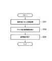
図7は、本発明の実施形態2に係る照明補正装置1Aを含む照明補正システム100における補正データ生成処理を示したフローチャートである。ここでは、有機ELパネル20Aが、基準有機ELパネル20Bが撮像された際の位置と同じ位置に設置されているとする。 FIG. 7 is a flowchart showing a correction data generation process in the
図7に示すように、照明補正システム100のカメラ3が、有機ELパネル20Aを撮像する(ステップS301)。 As shown in FIG. 7, the
次に、制御部10Aの輝度算出部16は、ブロック毎の対象輝度を算出する(ステップS303)。具体的には、輝度算出部16は、面発光する9つのブロック21〜29で配列された有機発光層32を有する有機ELパネル20Aをカメラ3で撮像した撮像データに基づいて、有機ELパネル20Aが有する有機発光層32の9つのブロック21〜29ごとの輝度を対象輝度として算出する。 Next, the
そして、補正データ生成部17は、メモリ12から基準輝度を読み込み(ステップS305)、カウンタkの値に初期値として、“1”を代入する(ステップS307)。 Then, the correction
次に、補正データ生成部17は、基準輝度算出部15により算出されたk番目のブロックの基準輝度が輝度算出部16により算出されたk番目のブロックの補正対象輝度より大きいか否かを判定する(ステップS309)。 Next, the correction
ステップS309において、基準輝度が補正対象輝度より大きいと判定された場合(YESの場合)、補正データ生成部17は、k番目のブロックの基準輝度からk番目のブロックの補正対象輝度を減算し、この減算した値(差分)に相当する電流値及び電圧値の補正データを算出する(ステップS311)。 When it is determined in step S309 that the reference luminance is greater than the correction target luminance (in the case of YES), the correction
例えば、補正データ生成部17は、図8に示す電流値又は電圧値に対する輝度の特性を示したグラフに基づいて、基準輝度から補正対象輝度を減算した値(差分)に相当する電流値及び電圧値の補正データを算出する。 For example, the correction
一方、ステップS309において、基準輝度が補正対象輝度以下であると判定された場合(NOの場合)、補正データ生成部17は、基準輝度算出部15により算出されたk番目のブロックの基準輝度が輝度算出部16により算出されたk番目のブロックの補正対象輝度より小さいか否かを判定する(ステップS313)。 On the other hand, when it is determined in step S309 that the reference luminance is equal to or lower than the correction target luminance (in the case of NO), the correction
ステップS313において、基準輝度が補正対象輝度より小さいと判定された場合(YESの場合)、補正データ生成部17は、k番目のブロックの補正対象輝度からk番目のブロックの基準輝度を減算し、この減算した値(差分)に相当する電流値及び電圧値の補正データを算出する(ステップS315)。 When it is determined in step S313 that the reference luminance is smaller than the correction target luminance (in the case of YES), the correction
具体的には、ステップS311における処理と同様に、補正データ生成部17は、図8に示す電流値又は電圧値に対する輝度の特性を示したグラフに基づいて、補正対象輝度から基準輝度を減算した値(差分)に相当する電流値及び電圧値の補正データを算出する。 Specifically, similarly to the processing in step S311, the correction
一方、ステップS313において、基準輝度が補正対象輝度より小さくないと判定された場合(NOの場合)、即ち、基準輝度と補正対象輝度とが同一であると判定された場合、補正データ生成部17は、9つのブロック21〜29分の補正データを算出したか否かを判定する(ステップS317)。 On the other hand, if it is determined in step S313 that the reference luminance is not smaller than the correction target luminance (in the case of NO), that is, if it is determined that the reference luminance and the correction target luminance are the same, the correction
ステップS317において、9つのブロック21〜29分の補正データを算出していないと判定された場合(NOの場合)、補正データ生成部17は、カウンタkの値に、“1”だけ加算する(ステップS319)。 When it is determined in step S317 that correction data for nine
一方、ステップS317において、9つのブロック21〜29分の補正データを算出したと判定された場合(YESの場合)、補正データ生成部17は、算出した補正データをメモリ12に書き込む(ステップS321)。具体的には、補正データ生成部17は、ブロック21〜29毎に、電流値及び電圧値それぞれの補正データを記憶させる。 On the other hand, if it is determined in step S317 that correction data for nine
以上のように、本発明の実施形態2に係る照明補正装置1Aによれば、輝度の基準となる複数のブロックで配列された有機発光層32を有する基準有機ELパネル20Bをカメラで撮像した撮像データに基づいて、基準有機ELパネル20Bが有する発光層32のブロックごとの輝度を基準輝度として算出する基準輝度算出部15と、有機ELパネル20Aをカメラ3で撮像した撮像データに基づいて、有機ELパネル20Aが有する発光層32のブロックごとの輝度を補正対象輝度として算出する輝度算出部16と、基準輝度に基づいて、補正対象輝度を補正するための補正データを生成し、メモリ12に記憶させる補正データ生成部17とを備えるので、有機ELパネル20Aが立体形状を有している場合においても、適切に輝度の均一化を行うことができる。 As described above, according to the
なお、本発明の実施形態2では、上下方向の中央部からカメラ3までの距離が相対的に短く、上下端部からカメラ3までの距離が相対的に長くなるように湾曲した有機ELパネル20Aを備えた照明補正装置1Aを例に挙げて説明したが、有機ELパネル20Aの形状は、この形状に限らず、どのような立体形状でもよい。 In Embodiment 2 of the present invention, the
また、本発明の実施形態2では、基準輝度算出部15と、輝度算出部16と、補正データ生成部17とを有する制御部10Aを備えた照明補正装置1Aを例に挙げて説明したが、これに限らない。基準輝度算出部15と、輝度算出部16と、補正データ生成部17とは、演算処理装置2が備える構成としてもよい。この場合、演算処理装置2が備える補正データ生成部17により生成されて供給された補正データをメモリ12に記憶する。これにより、照明補正装置1Aは、メモリ12に記憶された補正データに基づいて、複数のブロック間の輝度が均一になるように、ブロックごとに有機ELパネル20Aを発光させる制御設定値を決定することができるので、適切に輝度の均一化を行うことができる。 In the second embodiment of the present invention, the
さらに、本発明の実施形態1,2では、面発光する有機EL素子を用いて、ブロック21〜29で配列された有機発光層32を有する有機ELパネルを備えた照明補正装置1,1Aを例に挙げて説明したが、発光素子は、有機EL素子に限らず、他の自発光素子でもよい。即ち、面発光する素子であればよい。 Furthermore, in
1,1A…照明補正装置
2…演算処理装置
3…カメラ
10,10A…制御部
11…記憶制御部
12…メモリ
13…調光回路(決定部)
15…基準輝度算出部
16…輝度算出部
17…補正データ生成部
20,20A…有機ELパネル
20B…基準有機ELパネル
31…透明電極
32…有機発光層
33…背面電極
41…電源回路
42…調光入力部
100…照明補正システム
100…照明補正装置DESCRIPTION OF
DESCRIPTION OF
本発明は、面発光する照明装置に対して、照明の均一性を得るために照明装置への出力値を補正する照明補正装置に適用することができる。 INDUSTRIAL APPLICABILITY The present invention can be applied to an illumination correction apparatus that corrects an output value to an illumination apparatus in order to obtain illumination uniformity for an illumination apparatus that emits surface light.
Claims (5)
Translated fromJapaneseカメラにより前記発光パネルが撮像された撮像データに基づいて生成された補正データを記憶する記憶部と、
前記補正データに基づいて、前記複数のブロック間の輝度が均一になるように、前記ブロックごとに前記発光パネルを発光させる制御設定値を決定する決定部と、
を備えたことを特徴とする照明補正装置。A light-emitting panel having a light-emitting layer arranged in a plurality of blocks emitting surface light;
A storage unit for storing correction data generated based on imaging data obtained by imaging the light emitting panel by a camera;
A determining unit that determines a control setting value for causing the light-emitting panel to emit light for each block based on the correction data so that the luminance between the plurality of blocks is uniform;
An illumination correction apparatus comprising:
前記発光パネルを前記カメラで撮像した撮像データに基づいて、前記発光パネルが有する発光層のブロックごとの輝度を補正対象輝度として算出する輝度算出部と、
前記基準輝度に基づいて、前記補正対象輝度を補正するための前記補正データを生成し、前記記憶部に記憶させる補正データ生成部と、
を備えたことを特徴とする請求項1記載の照明補正装置。Based on imaging data obtained by imaging a reference light-emitting panel having a light-emitting layer arranged in a plurality of blocks serving as a reference for luminance with the camera, the luminance for each block of the light-emitting layer included in the reference light-emitting panel is calculated as the reference luminance. A reference luminance calculation unit;
Based on imaging data obtained by imaging the light emitting panel with the camera, a luminance calculating unit that calculates the luminance for each block of the light emitting layer of the light emitting panel as a correction target luminance;
A correction data generation unit that generates the correction data for correcting the correction target luminance based on the reference luminance and stores the correction data in the storage unit;
The illumination correction apparatus according to claim 1, further comprising:
ことを特徴とする請求項1又は2記載の照明補正装置。The illumination correction apparatus according to claim 1, wherein the light emitting layer is formed using a self-luminous element.
ことを特徴とする請求項1又は2記載の照明補正装置。The illumination correction apparatus according to claim 1, wherein the light emitting layer is formed using an organic EL element.
ことを特徴とする請求項2記載の照明補正装置。The illumination correction apparatus according to claim 2, wherein the light emitting panel and the reference light emitting panel have the same three-dimensional shape.
Priority Applications (1)
| Application Number | Priority Date | Filing Date | Title |
|---|---|---|---|
| JP2014501869AJPWO2013128565A1 (en) | 2012-02-28 | 2012-02-28 | Lighting correction device |
Applications Claiming Priority (1)
| Application Number | Priority Date | Filing Date | Title |
|---|---|---|---|
| JP2014501869AJPWO2013128565A1 (en) | 2012-02-28 | 2012-02-28 | Lighting correction device |
Publications (1)
| Publication Number | Publication Date |
|---|---|
| JPWO2013128565A1true JPWO2013128565A1 (en) | 2015-07-30 |
Family
ID=53770056
Family Applications (1)
| Application Number | Title | Priority Date | Filing Date |
|---|---|---|---|
| JP2014501869APendingJPWO2013128565A1 (en) | 2012-02-28 | 2012-02-28 | Lighting correction device |
Country Status (1)
| Country | Link |
|---|---|
| JP (1) | JPWO2013128565A1 (en) |
Citations (4)
| Publication number | Priority date | Publication date | Assignee | Title |
|---|---|---|---|---|
| JP2002169511A (en)* | 2000-09-19 | 2002-06-14 | Semiconductor Energy Lab Co Ltd | Luminous device and driving method therefor |
| JP2005316408A (en)* | 2004-03-30 | 2005-11-10 | Sanyo Electric Co Ltd | Device for generating correction value for display uneveness |
| JP2006091462A (en)* | 2004-09-24 | 2006-04-06 | Semiconductor Energy Lab Co Ltd | Display device |
| WO2008018500A1 (en)* | 2006-08-09 | 2008-02-14 | Tokyo Electron Limited | Film forming device, film forming system, and film forming method |
- 2012
- 2012-02-28JPJP2014501869Apatent/JPWO2013128565A1/enactivePending
Patent Citations (4)
| Publication number | Priority date | Publication date | Assignee | Title |
|---|---|---|---|---|
| JP2002169511A (en)* | 2000-09-19 | 2002-06-14 | Semiconductor Energy Lab Co Ltd | Luminous device and driving method therefor |
| JP2005316408A (en)* | 2004-03-30 | 2005-11-10 | Sanyo Electric Co Ltd | Device for generating correction value for display uneveness |
| JP2006091462A (en)* | 2004-09-24 | 2006-04-06 | Semiconductor Energy Lab Co Ltd | Display device |
| WO2008018500A1 (en)* | 2006-08-09 | 2008-02-14 | Tokyo Electron Limited | Film forming device, film forming system, and film forming method |
Similar Documents
| Publication | Publication Date | Title |
|---|---|---|
| US10297649B2 (en) | Light-emitting device, information processing device, and imaging device | |
| US9961726B2 (en) | Light-emitting device and camera | |
| RU2009149423A (en) | DISPLAY, METHOD AND COMPUTER SOFTWARE CORRECTION CORRECTION | |
| US20160171931A1 (en) | Reduced Image Sticking OLED Display | |
| CN106935196B (en) | Display device, optical compensation system and optical compensation method thereof | |
| CN103715369B (en) | One kind mixing escope and its control method | |
| JP2019061777A5 (en) | ||
| CN116229894A (en) | Display device and driving method thereof | |
| US20150070377A1 (en) | Image signal processing circuit, image signal processing method and display apparatus | |
| US9692955B1 (en) | Flash optimized using OLED display | |
| US9939262B2 (en) | Light-emitting device and camera | |
| WO2013128565A1 (en) | Illumination correction device | |
| JP4976605B1 (en) | Lighting device | |
| JPWO2013128565A1 (en) | Lighting correction device | |
| JP5642133B2 (en) | Image display device, image display method, and device for controlling image display device | |
| JP2013210510A5 (en) | ||
| WO2013175973A1 (en) | Evaluation method, evaluation device and evaluation program for color unevenness of surface light-emitting body | |
| JP4976604B1 (en) | Lighting device | |
| CN104318913B (en) | For the display control method and device of terminal | |
| CN109949727B (en) | Aging method and aging device for display panel | |
| CN112599096B (en) | Pixel driving structure, pixel driving method and display device | |
| JP2012129478A (en) | El module and lighting device | |
| CN109449191A (en) | A kind of OLED display panel and its control method, display device | |
| JP2016018149A5 (en) | ||
| CN105446536B (en) | Man-machine interactive system and its method |
Legal Events
| Date | Code | Title | Description |
|---|---|---|---|
| A02 | Decision of refusal | Free format text:JAPANESE INTERMEDIATE CODE: A02 Effective date:20150310 |