JPWO2013005655A1 - Light emitting device failure detector and light emitting device failure detection method - Google Patents
Light emitting device failure detector and light emitting device failure detection methodDownload PDFInfo
- Publication number
- JPWO2013005655A1 JPWO2013005655A1JP2013522965AJP2013522965AJPWO2013005655A1JP WO2013005655 A1JPWO2013005655 A1JP WO2013005655A1JP 2013522965 AJP2013522965 AJP 2013522965AJP 2013522965 AJP2013522965 AJP 2013522965AJP WO2013005655 A1JPWO2013005655 A1JP WO2013005655A1
- Authority
- JP
- Japan
- Prior art keywords
- emitting element
- current
- light emitting
- circuit
- light
- Prior art date
- Legal status (The legal status is an assumption and is not a legal conclusion. Google has not performed a legal analysis and makes no representation as to the accuracy of the status listed.)
- Granted
Links
- 238000001514detection methodMethods0.000titleclaimsabstractdescription53
- 238000007599dischargingMethods0.000claimsabstractdescription7
- 230000007274generation of a signal involved in cell-cell signalingEffects0.000claimsdescription17
- 239000003990capacitorSubstances0.000description7
- 230000007423decreaseEffects0.000description7
- 238000000034methodMethods0.000description7
- 230000032683agingEffects0.000description2
- 238000010586diagramMethods0.000description2
- 238000012986modificationMethods0.000description2
- 230000004048modificationEffects0.000description2
- 230000002123temporal effectEffects0.000description2
- 230000010485copingEffects0.000description1
- 230000000694effectsEffects0.000description1
- 238000005401electroluminescenceMethods0.000description1
- 230000007613environmental effectEffects0.000description1
- 230000005669field effectEffects0.000description1
- 238000005286illuminationMethods0.000description1
- 230000003287optical effectEffects0.000description1
- 230000035945sensitivityEffects0.000description1
Images


Classifications
- H—ELECTRICITY
- H05—ELECTRIC TECHNIQUES NOT OTHERWISE PROVIDED FOR
- H05B—ELECTRIC HEATING; ELECTRIC LIGHT SOURCES NOT OTHERWISE PROVIDED FOR; CIRCUIT ARRANGEMENTS FOR ELECTRIC LIGHT SOURCES, IN GENERAL
- H05B45/00—Circuit arrangements for operating light-emitting diodes [LED]
- H05B45/30—Driver circuits
- H05B45/37—Converter circuits
- H05B45/3725—Switched mode power supply [SMPS]
- G—PHYSICS
- G01—MEASURING; TESTING
- G01R—MEASURING ELECTRIC VARIABLES; MEASURING MAGNETIC VARIABLES
- G01R31/00—Arrangements for testing electric properties; Arrangements for locating electric faults; Arrangements for electrical testing characterised by what is being tested not provided for elsewhere
- G01R31/26—Testing of individual semiconductor devices
- G01R31/2601—Apparatus or methods therefor
- G—PHYSICS
- G01—MEASURING; TESTING
- G01R—MEASURING ELECTRIC VARIABLES; MEASURING MAGNETIC VARIABLES
- G01R31/00—Arrangements for testing electric properties; Arrangements for locating electric faults; Arrangements for electrical testing characterised by what is being tested not provided for elsewhere
- G01R31/26—Testing of individual semiconductor devices
- G01R31/2607—Circuits therefor
- G01R31/2632—Circuits therefor for testing diodes
- G01R31/2635—Testing light-emitting diodes, laser diodes or photodiodes
- H—ELECTRICITY
- H10—SEMICONDUCTOR DEVICES; ELECTRIC SOLID-STATE DEVICES NOT OTHERWISE PROVIDED FOR
- H10K—ORGANIC ELECTRIC SOLID-STATE DEVICES
- H10K71/00—Manufacture or treatment specially adapted for the organic devices covered by this subclass
- H10K71/861—Repairing
Landscapes
- Physics & Mathematics (AREA)
- General Physics & Mathematics (AREA)
- Optics & Photonics (AREA)
- Circuit Arrangement For Electric Light Sources In General (AREA)
- Testing Of Short-Circuits, Discontinuities, Leakage, Or Incorrect Line Connections (AREA)
- Electroluminescent Light Sources (AREA)
- Led Devices (AREA)
Abstract
Translated fromJapaneseDescription
Translated fromJapanese本発明は、発光素子の故障を検出する発光素子故障検出器及び発光素子故障検出方法に関する。 The present invention relates to a light emitting element failure detector and a light emitting element failure detecting method for detecting a failure of a light emitting element.
有機エレクトロルミネッセンス素子(以下有機EL素子)を照明装置の光源として使用することが提案されている。 It has been proposed to use an organic electroluminescence element (hereinafter referred to as an organic EL element) as a light source of an illumination device.
有機EL素子が短絡した場合、有機EL素子のアノード/カソード間のインピーダンスに応じた電圧Vfが、アノード/カソード間にかかる。この電圧Vfは正常な状態の有機EL素子のアノード/カソード間の電圧よりも低い。 When the organic EL element is short-circuited, a voltage Vf corresponding to the impedance between the anode and cathode of the organic EL element is applied between the anode and cathode. This voltage Vf is lower than the voltage between the anode and the cathode of the organic EL element in a normal state.
特許文献1に記載されている故障検出手段は、有機EL素子のアノード電極の電位Vfを測定する。アノード電極の電位Vfが基準電圧より低い場合、特許文献1の故障検出手段は、有機EL素子の短絡故障を検出する。 The failure detection means described in
また、有機EL素子が短絡した場合、有機EL素子のアノード/カソード間のインピーダンスが低下するため、有機EL素子に流れる電流が増加する。 Further, when the organic EL element is short-circuited, the impedance between the anode and the cathode of the organic EL element is lowered, and thus the current flowing through the organic EL element is increased.
特許文献2に記載されている故障検出手段は、有機EL素子に直列に接続した抵抗の電圧を測定する。電流の増加は、測定した電圧から検出できる。したがって、特許文献2の故障検出手段は、測定した電圧が所定の閾値を超えた場合、短絡故障を検出する。 The failure detection means described in
発光素子の短絡故障は、発光素子のアノード/カソード間の電圧Vf(出力電圧)の測定により、検出できる。 The short circuit failure of the light emitting element can be detected by measuring the voltage Vf (output voltage) between the anode and the cathode of the light emitting element.
特許文献3に記載されている回路保護部(故障検出手段)は、第1比較部と第2比較部とを備える。第1比較部は、LED(LIGHT EMITTING DIODE)の出力電圧が第1基準電圧より大きい場合、ハイレベルの電圧を出力する。また、第1比較部は、LEDの出力電圧が第1基準電圧より小さい場合、ローレベルの電圧を出力する。第2比較部は、第1比較部の出力電圧と第2基準電圧とを比較する。第2比較部は、その結果に応じてローレベル又はハイレベルの電圧を出力する。回路保護部は第1比較部、第2比較部の出力電圧から短絡故障を検出する。 The circuit protection unit (failure detection means) described in Patent Document 3 includes a first comparison unit and a second comparison unit. A 1st comparison part outputs a high level voltage, when the output voltage of LED (LIGHT MITTING DIODE) is larger than a 1st reference voltage. In addition, the first comparison unit outputs a low level voltage when the output voltage of the LED is smaller than the first reference voltage. The second comparison unit compares the output voltage of the first comparison unit with the second reference voltage. The second comparison unit outputs a low level or high level voltage according to the result. The circuit protection unit detects a short-circuit failure from the output voltages of the first comparison unit and the second comparison unit.
上記の故障検出手段は、発光素子のアノード/カソード間電圧Vf、又はVfに関連する電圧を測定する。そして、これらの故障検出手段は、測定した電圧と基準電圧から、発光素子の短絡故障を検出する。 The failure detection means measures the anode / cathode voltage Vf of the light emitting element or a voltage related to Vf. These failure detection means detect a short-circuit failure of the light emitting element from the measured voltage and the reference voltage.
発光素子のアノード/カソード間電圧Vfは、素子のV−I特性、経時変化、環境温度等により異なる。また、発光素子の電圧Vfは、短絡した発光素子のアノード/カソード間のインピーダンスによっても変化する。 The anode / cathode voltage Vf of the light emitting element varies depending on the VI characteristics of the element, change with time, environmental temperature, and the like. The voltage Vf of the light emitting element also varies depending on the impedance between the anode and the cathode of the shorted light emitting element.
本発明は、上記の事情に鑑みてなされたものであり、発光素子のアノード/カソード間電圧Vfのばらつき、変化、変動に影響されずに、短絡故障を検出できる発光素子故障検出器及び発光素子故障検出方法を提供することを目的とする。 The present invention has been made in view of the above circumstances, and a light-emitting element failure detector and a light-emitting element capable of detecting a short-circuit failure without being affected by variations, changes, and fluctuations in the anode-cathode voltage Vf of the light-emitting element. An object is to provide a failure detection method.
前記の目的を達成するために、本願発明の第1の観点に係る発光素子故障検出器は、
発光素子と、該発光素子への電流供給路と、該電流供給路を介して前記発光素子に電流を供給する定電流回路と、前記定電流回路が前記発光素子への電流供給を停止した場合に前記発光素子及びその両電極間に接続する部位に蓄積する電荷を放電する放電路と、を備える発光素子回路中の前記発光素子の短絡を検出する発光素子故障検出器において、
前記放電路とは異なる前記電流供給路に配置され、前記定電流回路が前記発光素子に供給する電流を瞬断する電流瞬断回路と、
前記発光素子の前記アノードと前記カソードとの間に、発光素子と並列に接続される並列電路を備え、
前記並列電路は、
ダイオードと、
前記発光素子が正常な状態でのアノード/カソード間の電圧よりも小さい正値の直流の基準電圧を発生する直流電源と、
電流検出部と、を備え、
前記ダイオードと、前記直流電源と、前記電流検出部とが直列に接続されるとともに、前記ダイオードのカソードと前記直流電源の陽極とが、それぞれ前記発光素子の前記アノードの側に配置されるように前記ダイオードと前記直流電源とが接続され、
前記電流検出部は、前記電流瞬断回路で電流を瞬断した期間の前記並列電路の電流の有無を検出する、
ことを特徴とする。In order to achieve the above object, a light-emitting element failure detector according to the first aspect of the present invention comprises:
A light-emitting element, a current supply path to the light-emitting element, a constant-current circuit that supplies current to the light-emitting element through the current supply path, and the constant-current circuit stops supplying current to the light-emitting element In the light emitting element failure detector for detecting a short circuit of the light emitting element in the light emitting element circuit, comprising: a discharge path for discharging the charge accumulated in the light emitting element and a portion connected between the electrodes.
A current interruption circuit that is arranged in the current supply path different from the discharge path, and that instantaneously interrupts the current that the constant current circuit supplies to the light emitting element;
A parallel electric circuit connected in parallel with the light emitting element is provided between the anode and the cathode of the light emitting element,
The parallel circuit is
A diode,
A direct-current power source that generates a positive direct-current reference voltage that is smaller than the voltage between the anode and the cathode when the light-emitting element is in a normal state;
A current detection unit,
The diode, the DC power supply, and the current detection unit are connected in series, and the cathode of the diode and the anode of the DC power supply are respectively disposed on the anode side of the light emitting element. The diode and the DC power supply are connected;
The current detection unit detects the presence or absence of current in the parallel circuit during a period in which the current is instantaneously interrupted by the current instantaneous interruption circuit.
It is characterized by that.
本願発明の第2の観点に係る発光素子故障検出方法は、
発光素子と、該発光素子への電流供給路と、該電流供給路を介して前記発光素子に電流を供給する定電流回路と、前記定電流回路が前記発光素子への電流供給を停止した場合に前記発光素子及びその両電極間に接続する部分に蓄積する電荷を放電する放電路と、を備える発光素子回路中の前記発光素子の短絡を検出する発光素子故障検出方法において、
前記放電路とは異なる前記電流供給路で、前記定電流回路が前記発光素子に供給する電流を瞬断する電流瞬断ステップと、
前記発光素子が正常な状態でのアノード/カソード間の電圧よりも小さい正値の直流の基準電圧を発生する直流電源とダイオードが直列に接続されるとともに、前記発光素子の前記アノードと前記カソードとの間に、前記発光素子と並列に接続されて構成される並列電路で、前記ダイオードのカソードと前記直流電源の陽極が、それぞれ前記発光素子の前記アノード側に配置されるように前記ダイオードと前記直流電源が接続された状態で、前記電流瞬断ステップで電流を瞬断した期間の前記並列電路での電流の有無を検出する電流検出ステップと、
を備えることを特徴とする。The light emitting element failure detection method according to the second aspect of the present invention is:
A light-emitting element, a current supply path to the light-emitting element, a constant-current circuit that supplies current to the light-emitting element through the current supply path, and the constant-current circuit stops supplying current to the light-emitting element In the light emitting element failure detection method for detecting a short circuit of the light emitting element in the light emitting element circuit, comprising: a discharge path for discharging charges accumulated in the light emitting element and a portion connected between the light emitting element and the electrode;
In the current supply path different from the discharge path, a current instantaneous interruption step of instantaneously interrupting the current supplied to the light emitting element by the constant current circuit;
A direct current power source for generating a positive DC reference voltage smaller than the voltage between the anode and the cathode in a normal state of the light emitting element and a diode are connected in series, and the anode and the cathode of the light emitting element Between the diode and the diode such that the cathode of the diode and the anode of the DC power source are arranged on the anode side of the light emitting element, respectively, in a parallel circuit configured to be connected in parallel with the light emitting element. In a state where a DC power source is connected, a current detection step for detecting the presence or absence of current in the parallel circuit during a period in which current is instantaneously interrupted in the current instantaneous interruption step;
It is characterized by providing.
本発明によれば、発光素子のアノード/カソード間電圧Vfのばらつき、変化、変動等に影響されずに、短絡故障を検出できる発光素子故障検出器及び発光素子故障検出方法を提供できる。 According to the present invention, it is possible to provide a light emitting element failure detector and a light emitting element failure detecting method capable of detecting a short circuit failure without being affected by variations, changes, fluctuations, etc., of the anode / cathode voltage Vf of the light emitting element.
(実施形態1)
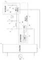
図1は、本発明の実施形態1に係る発光素子故障検出器を含む発光素子回路の構成を示す。発光素子回路は、発光素子1と、発光素子1に所定の電流を供給する定電流回路2と、定電流回路2に電力を供給する交流電源3と、発光素子1の短絡を検出する発光素子故障検出器4とを備える。また、発光素子故障検出器4は、電流瞬断回路5と、故障検出部6とを備える。(Embodiment 1)
FIG. 1 shows a configuration of a light emitting element circuit including a light emitting element failure detector according to
発光素子回路では、静電容量が発光素子1に並列に接続されると見なされる。コンデンサ7は、この静電容量を示す(図1)。また、ダイオード8が、コンデンサ7及び発光素子1に並列に接続される。さらに、コイル9が、コンデンサ7及び発光素子1と、ダイオード8とを接続する電路の少なくとも一方に接続される。ダイオード8は、並列に接続された発光素子1の極性とは逆向きの極性で配置される。コンデンサ7と、発光素子1と、コイル9と、ダイオード8は、放電路を形成する。この放電路は、発光素子1への電流供給が停止した場合に、発光素子1とコンデンサ7が蓄積する電荷を放電する。なお、コイル9は抵抗でもよい。 In the light emitting element circuit, the capacitance is considered to be connected to the
抵抗10は発光素子1に直列に接続される。定電流回路3は、抵抗10を介して発光素子1に電流を供給する。 The
電流瞬断回路5は、スイッチ部50とスイッチ制御部51とを備える。スイッチ部50は、電流の供給と停止の切り換えにより、電流を瞬断する。スイッチ制御部51は、スイッチ部50の切り換えを制御することにより、電流の瞬断を制御する。 The instantaneous
スイッチ部50は、例えば、FET(Field Effect Transistor)で構成される。スイッチ部50は、定電流回路2から発光素子1への電流供給路上であって、放電路とは異なる位置に配置される。 The
スイッチ制御部51は、所定のタイミングでスイッチ部50にON/OFF切り換え信号を出力する。スイッチ部50がFETの場合、スイッチ制御部51は切り換え信号をFETのゲート電極に出力する。 The
故障検出部6は、ダイオード60、直流電源61、電流検出部62を備える。また、ダイオード60、直流電源61、電流検出部62は、互いに直列に接続される。故障検出部6は発光素子1のアノードとカソードとの間に接続される。従って、ダイオード60、直流電源61、電流検出部62は、発光素子1に並列に接続された並列電路を形成する。この並列電路の中で、ダイオード60のカソード、直流電源61の陽極は、それぞれ発光素子1のアノード側に配置される。 The failure detection unit 6 includes a
直流電源61は、直流の基準電圧Vcを発生する。基準電圧Vcは、正常な状態での発光素子1のアノード/カソード間の電圧Vfよりも小さい正値に設定される。基準電圧Vcの詳細については後述する。なお、正常な状態は、短絡が生じていない状態を指す。 The
電流検出部62は、並列電路に流れる電流を検出する。電流検出部62は、例えば、電流計で構成される。電流検出部62の出力信号は、例えば、定電流回路2の電流供給を停止する信号の入力端子(制御入力端子)に入力される。 The
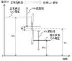
図2Aは、正常な状態の発光素子1(有機EL素子)に対して電流が瞬断した場合の、発光素子1に流れる電流と発光素子1のアノード/カソード間の電圧Vfの時間変化を示す。図2Bは、短絡した発光素子1に対して電流が瞬断した場合の、発光素子1に流れる電流と発光素子1のアノード/カソード間の電圧Vfの時間変化を示す。 FIG. 2A shows temporal changes in the current flowing through the light-emitting
正常な状態の発光素子1のアノード/カソード間電圧VfをVfnと仮定する。電流が瞬断した場合、図2Aに示すように、電圧VfはVfnからVfn0へわずかに低下する。すなわち、電圧Vfは急速に0Vに低下しない。これは、コンデンサ7と発光素子1が蓄積する電荷が放電路を介して放電される時定数が大きいためである。It is assumed that the anode / cathode voltage Vf of the
一方、発光素子1が短絡した場合、発光素子1は等価回路として、小さな抵抗値を有する抵抗に置き換えできる。したがって、発光素子1の電圧VfはVfnよりも小さいVfaに低下する。また、短絡した発光素子1においては、放電時定数が小さいため、発光素子1の電圧Vfは電流の瞬断により0Vに急減する(図2B)。 On the other hand, when the
瞬断の期間は、短絡した発光素子1において電圧Vfが0Vに低下する時間以上、且つ、瞬断による発光素子1の発光停止が観察者に認識されない時間に設定する。この瞬断の期間はあらかじめ計算又は試行により求められる。なお、発光素子1の発光停止が観察者に認識されない瞬断では、正常な状態の発光素子1の電圧Vfは0Vにまで低下しない。 The momentary interruption period is set to a time longer than the time when the voltage Vf decreases to 0 V in the short-circuited
従って、短絡故障検出の閾値はVfn0よりも小さく、0Vよりも大きく設定される。電流の瞬断により電圧Vfが閾値以下に低下した場合、発光素子故障検出器4は短絡を検出する。Therefore, the threshold for short circuit failure detection is set to be smaller than Vfn0 and larger than 0V. When the voltage Vf drops below the threshold due to the instantaneous interruption of the current, the light emitting element failure detector 4 detects a short circuit.
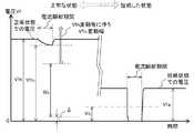
閾値の設定について従来例と比較して説明する(図3A、図3B)。従来は、図3Aに示すように、閾値は、VfnとVfaの間に設定される。そして、従来の発光素子故障検出器はVfが閾値以下であるかどうかにより短絡を検出する。Vfnは、発光素子1のV−I特性のばらつき、温度変化、経年変化により大きく変動する。また、Vfaは短絡した発光素子1の抵抗成分に依存するので、Vfaは、短絡の状態により、大きく変動する。したがって、閾値は、VfnとVfaの変動を予測した後、どちらの変動範囲にも属さない範囲W内に設定される。この範囲Wは狭いため、閾値の設定は難しい。 The setting of the threshold will be described in comparison with the conventional example (FIGS. 3A and 3B). Conventionally, as shown in FIG. 3A, the threshold value is set between Vfn and Vfa. The conventional light emitting element failure detector detects a short circuit depending on whether Vf is equal to or less than a threshold value. Vfn largely fluctuates due to variations in the VI characteristics of the
一方、本実施形態において電流が瞬断した場合、正常な状態の発光素子1の電圧VfはVfn0にわずかに低下する。本実施形態において電流が瞬断した場合、短絡した発光素子1の電圧Vfは0Vに急激に低下する。図3Bに示すように、Vfn0は、発光素子1のV−I特性のばらつき、温度変化、経年変化により変動するので、閾値は、Vfn0の変動の下限よりも小さく、且つ、0Vよりも大きく設定される(図3B)。この範囲W0は、従来例の範囲Wに比べ、非常に広い。なお、0Vよりも大きいとは、実用的には、0Vに裕度Δを加えた値よりも大きいことを指す。裕度Δは、正値であればよい。例えば、裕度Δは、電圧Vfが0V近傍で有する揺らぎ幅の1/2に設定される。On the other hand, if the current in the present embodiment is instantaneously interrupted, the voltage Vf of the light-emitting
閾値とfa(図3B)との大小関係については考慮する必要はない。閾値がVfaより大きい場合、電流の瞬断なしに、電流が短絡した発光素子1に接続する並列電路に流れる。また、閾値がVfaより小さい場合、電流の瞬断により、電流が短絡した発光素子1に接続する並列電路に流れる。したがって、発光素子故障検出器4は、閾値とVfa(図3B)との大小関係に関係なく、発光素子1の短絡を検出できる。 There is no need to consider the magnitude relationship between the threshold and fa (FIG. 3B). When the threshold value is larger than Vfa, the current flows through the parallel circuit connected to the light-emitting
上述のような閾値の設定により、発光素子故障検出器4は、電流瞬断により発光素子1のアノード/カソード間の電圧Vfが閾値よりも小さい場合を短絡故障として検出できる。 By setting the threshold value as described above, the light emitting element failure detector 4 can detect a case where the voltage Vf between the anode and the cathode of the
図1に示す発光素子故障検出器4の動作を具体的に説明する。発光素子故障検出器4における直流電源61の基準電圧Vcは、上述した閾値に等しく設定される。 The operation of the light emitting element failure detector 4 shown in FIG. 1 will be specifically described. The reference voltage Vc of the
図1において、ダイオード60のカソード電位は、発光素子1のアノードと同電位である。発光素子1が正常な状態の場合、ダイオード60のカソード電位は、発光素子1のカソード電位よりもVf高い。また、ダイオード60のアノード電位は、電流が並列電路に流れていない場合、発光素子1のカソード電位よりもVc高い。基準電圧Vcは閾値と等しいので、直流電源61のVcは、正常な状態の発光素子1のアノード/カソード間電圧Vfより小さい。したがって、Vf−Vcの逆方向の電圧が、ダイオード60のアノード/カソード間にかかる。そのため、発光素子1が正常な状態の場合、電流は故障検出部6の並列電路に流れない。よって、電流検出部62は電流を検出しない。 In FIG. 1, the cathode potential of the
電流瞬断回路5が、正常な状態の発光素子1への電流供給を瞬断した場合、Vfn0−Vcの電圧がダイオード60のカソード/アノード間にかかる。基準電圧Vcは閾値に等しいので、VcはVfn0の最小値よりも小さい。従って、逆方向の電圧がダイオード60にかかる。よって、電流は並列電路に流れない。When the instantaneous
一方、短絡した発光素子1への電流が瞬断した場合、発光素子1のアノード/カソード間電圧Vfは急速に0Vに低下する。基準電圧Vcは0Vより大きいので、順方向の電圧Vcがダイオード60にかかる。そして、電流が故障検出部6の並列電路に流れる。電流検出部62が、この電流を検出することにより、発光素子故障検出器4は発光素子1の短絡を検出する。 On the other hand, when the current to the short-circuited
並列電路の電流値は、電流検出部62で検出できる値あればよい。ダイオード60の電流は順方向の電圧に依存する。従って、基準電圧Vcは、電流検出部62の感度、ダイオード60のV−I特性を考慮して、設定される。 The current value of the parallel circuit may be a value that can be detected by the
電流検出部62の出力端子と定電流回路2の制御入力端子との接続により、発光素子故障検出器4は、定電流回路2から発光素子1への電流供給を停止できる。 By connecting the output terminal of the
図4は発光素子故障検出処理フローチャートを示す。 FIG. 4 shows a light emitting element failure detection processing flowchart.
交流電源3がON状態にされる。これにより、定電流回路2は発光素子1へ電流を供給する。電流が供給された発光素子1は発光する(ステップS1)。 The AC power supply 3 is turned on. Thereby, the constant
次に、電流瞬断回路5は、所定のタイミングで発光素子1への電流供給を瞬断する(ステップS2)。電流検出部62は、並列電路に電流が流れたかどうかを検出する(ステップS3)。電流が検出された場合(ステップS3;YES)、電流検出部62の出力により、定められた短絡に対処する処置が実行される(ステップS4)。これにより、発光素子故障検出処理は終了する。電流が検出されない場合(ステップS3;NO)、発光素子故障検出処理は、ステップS2に戻る。電流検出部62は、電流検出を継続する。なお、電流が検知された場合とは、実用的には電流値が所定の閾値を超えたかどうかにより判別できる。定められた短絡に対処する処置とは、例えば、定電流回路2が発光素子1への電流供給を停止する処置である。 Next, the instantaneous
本実施形態1によれば、基準電圧Vcは、発光素子1のアノード/カソード間電圧Vfのばらつき、変化、変動等に影響されずに、設定される。したがって、本実施形態によれば、発光素子1のアノード/カソード間電圧Vfのばらつき、変化、変動に影響されずに短絡故障を検出できる発光素子故障検出器4及び発光素子故障検出方法を提供できる。 According to the first embodiment, the reference voltage Vc is set without being affected by variations, changes, fluctuations, and the like of the anode / cathode voltage Vf of the
なお、発光素子1のアノード/カソードの配置の向きに対するダイオード60のアノード/カソードの配置の向き、直流電源61の陽極/陰極の配置の向きは、図1に示すとおりであればよい。すなわち、ダイオード60、直流電源61、電流検出部62の配列順序は特に制限されない。 The orientation of the anode / cathode arrangement of the
複数の発光素子1を直列に接続した場合、故障検出部6は、各発光素子1のアノード/カソード間にそれぞれ設置される。これにより、発光素子故障検出器4は、直列に接続した複数の発光素子1の短絡を検出できる。この電流の供給の停止により、複数の発光素子1における短絡の連鎖が防げる。 When a plurality of
(実施形態2)
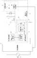
図5は、実施形態2に係る発光素子故障検出器4を備える発光素子回路の構成を示す。本実施形態においては、発光素子回路は、発光素子1の調光制御にPWM(Pulse Width Modulation)制御を使用する。(Embodiment 2)
FIG. 5 shows a configuration of a light emitting element circuit including the light emitting element failure detector 4 according to the second embodiment. In the present embodiment, the light emitting element circuit uses PWM (Pulse Width Modulation) control for dimming control of the
PWM制御においては、所定周波数のパルス列が発光素子1に供給される。発光素子1の調光は、供給されるパルスのパルス幅により制御される。 In the PWM control, a pulse train having a predetermined frequency is supplied to the
本実施形態の光素子回路は、PWM調光回路11を備える。PWM調光回路11は、電流制御スイッチ110と調光レベル設定部111とPWM信号生成部112と駆動回路113とを備える。電流制御スイッチ110は、放電路とは異なる発光素子1への電流供給路に設置される。また、電流制御スイッチ110は、発光素子1への電流供給のON/OFF制御を行う。電流制御スイッチ110は、例えば、FETで構成される(図5)。調光レベル設定部111は、発光素子1の調光レベルを設定する。PWM信号生成部112は、設定された調光レベルからパルス幅を選択する。PWM信号生成部112は、選択されたパルス幅を有する所定周波数のパルス列(PWM信号)を生成する。駆動回路113は、PWM信号に従って、電流制御スイッチ110による電流供給のON/OFFを制御する。その他の構成は実施形態1と同じである。 The optical element circuit of this embodiment includes a PWM dimming circuit 11. The PWM dimming circuit 11 includes a
実施形態2では、実施形態1における電流瞬断回路5はPWM調光回路11の一部で構成される。具体的には、電流制御スイッチ111は、実施形態1におけるスイッチ部50を兼用する。また、PWM信号生成部112と駆動回路113が、実施形態1におけるスイッチ制御部51を兼用する。 In the second embodiment, the instantaneous
実施形態2は、PWM信号生成部112が、所定の周期でパルス列の一部を連続して間引いてパルス列を生成することを特徴とする。例えば、Nパルス当たり1パルス又は複数のパルスがパルス列から連続して間引かれる。この間引きにより生じるパルスの存在しない期間が、実施形態1における電流の瞬断の期間に相当する。 The second embodiment is characterized in that the PWM
実施形態2では、電流が発光素子1にパルス列で供給されるため、電流の瞬断が絶えず起こる。従って、パルス列に応じて電圧の低下も絶えず生じる。しかし、パルス列が連続している場合、瞬断の期間は非常に短いので、電圧Vfが0Vまで急激に低下しない。PWM信号生成部112は、発光素子1が短絡した状態において、電圧Vfが0Vまで低下する時間とパルス幅から、連続して間引くパルス数を選択する。瞬断の期間の設定は実施形態1と同様である。パルス幅は、PWM信号生成部112により、調光レベルに応じて選択される。 In
本実施形態の動作は、瞬断の方法を除き、実施形態1と同様である。 The operation of this embodiment is the same as that of
実施形態2によれば、PWM信号生成部112は所定の周期でパルスを間引いたパルス列を生成する。この間引かれたパルス列を発光素子1に供給することにより、PWM信号生成部112と駆動回路113が、実施形態1におけるスイッチ制御部51の機能を兼ね備える。また、電流制御スイッチ110は実施形態1におけるスイッチ部50の機能を兼ね備える。実施形態2によれば、新たなハードウェアの追加なしに、電流瞬断回路5を実現できる。本実施形態における発光素子故障検出器4は実施形態1に記載の効果と同様の効果を奏する。 According to the second embodiment, the PWM
上記の実施形態の一部又は全部は、以下の付記のようにも記載されうるが、以下には限られない。 A part or all of the above-described embodiment can be described as in the following supplementary notes, but is not limited thereto.
(付記1)
発光素子と、該発光素子への電流供給路と、該電流供給路を介して前記発光素子に電流を供給する定電流回路と、前記定電流回路が前記発光素子への電流供給を停止した場合に前記発光素子及びその両電極間に接続する部位に蓄積する電荷を放電する放電路と、を備える発光素子回路中の前記発光素子の短絡を検出する発光素子故障検出器において、
前記放電路とは異なる前記電流供給路に配置され、前記定電流回路が前記発光素子に供給する電流を瞬断する電流瞬断回路と、
前記発光素子の前記アノードと前記カソードとの間に、発光素子と並列に接続される並列電路を備え、
前記並列電路は、
ダイオードと、
前記発光素子が正常状態でのアノード/カソード間の電圧よりも小さい正値の直流の基準電圧を発生する直流電源と、
電流検出部と、を備え、
前記ダイオードと、前記直流電源と、前記電流検出部とが直列に接続されるとともに、前記ダイオードのカソードと前記直流電源の陽極とが、それぞれ前記発光素子の前記アノードの側に配置されるように前記ダイオードと前記直流電源とが接続され、
前記電流検出部は、前記電流瞬断回路で電流を瞬断した期間の前記並列電路の電流の有無を検出する、
ことを特徴とする発光素子故障検出器。(Appendix 1)
A light-emitting element, a current supply path to the light-emitting element, a constant-current circuit that supplies current to the light-emitting element through the current supply path, and the constant-current circuit stops supplying current to the light-emitting element In the light emitting element failure detector for detecting a short circuit of the light emitting element in the light emitting element circuit, comprising: a discharge path for discharging the charge accumulated in the light emitting element and a portion connected between the electrodes.
A current interruption circuit that is arranged in the current supply path different from the discharge path, and that instantaneously interrupts the current that the constant current circuit supplies to the light emitting element;
A parallel electric circuit connected in parallel with the light emitting element is provided between the anode and the cathode of the light emitting element,
The parallel circuit is
A diode,
A direct current power source for generating a positive direct current reference voltage smaller than the voltage between the anode and the cathode when the light emitting element is in a normal state;
A current detection unit,
The diode, the DC power supply, and the current detection unit are connected in series, and the cathode of the diode and the anode of the DC power supply are respectively disposed on the anode side of the light emitting element. The diode and the DC power supply are connected;
The current detection unit detects the presence or absence of current in the parallel circuit during a period in which the current is instantaneously interrupted by the current instantaneous interruption circuit.
A light emitting device failure detector.
(付記2)
前記電流瞬断回路は、
前記定電流回路から前記発光素子への電流の供給と停止を切り換えるスイッチ部と、
該スイッチ部の前記切り換えを制御するスイッチ制御部と、を備える、
ことを特徴とする付記1に記載の発光素子故障検出器。(Appendix 2)
The current interruption circuit is
A switch unit for switching supply and stop of current from the constant current circuit to the light emitting element;
A switch control unit that controls the switching of the switch unit,
The light emitting element failure detector according to
(付記3)
前記発光素子回路は、設定された調光レベルに基づきパルス幅を設定し、該設定したパルス幅のパルス列からなるPWM信号を生成するPWM信号生成部と、該PWM信号生成部で生成された前記PWM信号を受け、該PWM信号と同じパターンのパルス列からなるPWM制御信号を出力する駆動回路と、前記電流供給路に設置され、前記PWM制御信号を入力し、該PWM制御信号により、前記発光素子への電流の供給と停止を切り換える電流制御スイッチと、を更に備え、
前記PWM信号生成部は、前記パルス列から所定の周期で少なくとも1パルス以上のパルスを連続して除いて前記PWM信号を生成し、該生成されたPWM信号を前記駆動回路に供給し、
前記放電路と異なる前記電流供給路に設置された前記電流制御スイッチは、前記スイッチ部を兼用し、
前記パルスが連続して除かれたことによるパルスの存在しない期間を、前記電流を瞬断した期間とすることにより、前記PWM信号生成部と前記駆動回路が前記スイッチ制御部を兼用する
ことを特徴とする付記2に記載の発光素子故障検出器。(Appendix 3)
The light emitting element circuit sets a pulse width based on the set dimming level, generates a PWM signal composed of a pulse train of the set pulse width, and the PWM signal generation unit generates the PWM signal. A drive circuit that receives a PWM signal and outputs a PWM control signal composed of a pulse train of the same pattern as the PWM signal, and is installed in the current supply path, receives the PWM control signal, and the light emitting element is input by the PWM control signal A current control switch that switches between supply and stop of current to
The PWM signal generation unit generates the PWM signal by continuously removing at least one pulse or more from the pulse train at a predetermined cycle, and supplies the generated PWM signal to the drive circuit,
The current control switch installed in the current supply path different from the discharge path also serves as the switch section,
The PWM signal generation unit and the drive circuit also serve as the switch control unit by setting a period in which there is no pulse due to continuous removal of the pulse as a period in which the current is momentarily interrupted. The light emitting element failure detector according to
(付記4)
前記PWM信号生成部は、前記設定されたパルス幅と、あらかじめ設定された前記瞬断の期間とから前記連続して除くパルスの数を選択する、
ことを特徴とする付記3に記載の発光素子故障検出器。(Appendix 4)
The PWM signal generation unit selects the number of pulses to be continuously removed from the set pulse width and the preset interruption period.
The light emitting element failure detector according to appendix 3, wherein
(付記5)
前記発光素子は、有機EL素子である、
ことを特徴とする付記1乃至4のいずれか1に記載の発光素子故障検出器。(Appendix 5)
The light emitting element is an organic EL element.
The light emitting element failure detector according to any one of
(付記6)
前記発光素子は、LED素子である、
ことを特徴とする付記1乃至4のいずれか1に記載の発光素子故障検出器。(Appendix 6)
The light emitting element is an LED element.
The light emitting element failure detector according to any one of
(付記7)
発光素子と、該発光素子への電流供給路と、該電流供給路を介して前記発光素子に電流を供給する定電流回路と、前記定電流回路が前記発光素子への電流供給を停止した場合に前記発光素子及びその両電極間に接続する部分に蓄積する電荷を放電する放電路と、を備える発光素子回路中の前記発光素子の短絡を検出する発光素子故障検出方法において、
前記放電路とは異なる前記電流供給路で、前記定電流回路が前記発光素子に供給する電流を瞬断する電流瞬断ステップと、
前記発光素子が正常な状態でのアノード/カソード間の電圧よりも小さい正値の直流の基準電圧を発生する直流電源とダイオードが直列に接続されるとともに、前記発光素子の前記アノードと前記カソードとの間に、前記発光素子と並列に接続されて構成される並列電路で、前記ダイオードのカソードと前記直流電源の陽極が、それぞれ前記発光素子の前記アノード側に配置されるように前記ダイオードと前記直流電源が接続された状態で、前記電流瞬断ステップで電流を瞬断した期間の前記並列電路での電流の有無を検出する電流検出ステップと、
を備えることを特徴とする発光素子故障検出方法。(Appendix 7)
A light-emitting element, a current supply path to the light-emitting element, a constant-current circuit that supplies current to the light-emitting element through the current supply path, and the constant-current circuit stops supplying current to the light-emitting element In the light emitting element failure detection method for detecting a short circuit of the light emitting element in the light emitting element circuit, comprising: a discharge path for discharging charges accumulated in the light emitting element and a portion connected between the light emitting element and the electrode;
In the current supply path different from the discharge path, a current instantaneous interruption step of instantaneously interrupting the current supplied to the light emitting element by the constant current circuit;
A direct current power source for generating a positive DC reference voltage smaller than the voltage between the anode and the cathode in a normal state of the light emitting element and a diode are connected in series, and the anode and the cathode of the light emitting element Between the diode and the diode such that the cathode of the diode and the anode of the DC power source are arranged on the anode side of the light emitting element, respectively, in a parallel circuit configured to be connected in parallel with the light emitting element. In a state where a DC power source is connected, a current detection step for detecting the presence or absence of current in the parallel circuit during a period in which current is instantaneously interrupted in the current instantaneous interruption step;
A light emitting element failure detection method comprising:
本発明は、本発明の広義の精神と範囲を逸脱することなく、様々な実施の形態及び変形が可能とされるものである。また、上述した実施の形態は、本発明を説明するためのものであり、本発明の範囲を限定するものではない。すなわち、本発明の範囲は、実施の形態ではなく、請求の範囲によって示される。そして、請求の範囲内及びそれと同等の発明の意義の範囲内で施される様々な変形が、本発明の範囲内とみなされる。 Various embodiments and modifications can be made to the present invention without departing from the broad spirit and scope of the present invention. The above-described embodiments are for explaining the present invention and do not limit the scope of the present invention. In other words, the scope of the present invention is shown not by the embodiments but by the claims. Various modifications within the scope of the claims and within the scope of the equivalent invention are considered to be within the scope of the present invention.
本発明は、2011年7月5日に出願された日本国特許出願2011−148785号に基づく。本明細書中に日本国特許出願2011−148785号の明細書、特許請求の範囲、図面全体を参照として取り込むものとする。 The present invention is based on Japanese Patent Application No. 2011-148785 filed on July 5, 2011. In this specification, the specification of Japanese Patent Application No. 2011-148785, the claims, and the entire drawing are incorporated as references.
本発明は、発光素子、発光素子を使用する各分野に利用することができる。 The present invention can be used in light emitting elements and various fields using light emitting elements.
1 発光素子
2 定電流回路
3 交流電源
4 発光素子故障検出器
5 電流瞬断回路
6 故障検出部
7 コンデンサ
8 ダイオード
9 コイル
10 抵抗
11 PWM調光回路
50 スイッチ部
51 スイッチ制御部
60 ダイオード
61 直流電源
62 電流検出部
110 電流制御スイッチ
111 調光レベル設定部
112 PWM信号生成部
113 駆動回路1 Light emitting element
2 Constant current circuit
3 AC power supply
4 Light emitting device failure detector
5 Current interruption circuit
6 Failure detection unit
7 capacitors
8 Diode
DESCRIPTION OF
Claims (7)
Translated fromJapanese前記放電路とは異なる前記電流供給路に配置され、前記定電流回路が前記発光素子に供給する電流を瞬断する電流瞬断回路と、
前記発光素子の前記アノードと前記カソードとの間に、発光素子と並列に接続される並列電路を備え、
前記並列電路は、
ダイオードと、
前記発光素子が正常状態でのアノード/カソード間の電圧よりも小さい正値の直流の基準電圧を発生する直流電源と、
電流検出部と、を備え、
前記ダイオードと、前記直流電源と、前記電流検出部とが直列に接続されるとともに、前記ダイオードのカソードと前記直流電源の陽極とが、それぞれ前記発光素子の前記アノードの側に配置されるように前記ダイオードと前記直流電源とが接続され、
前記電流検出部は、前記電流瞬断回路で電流を瞬断した期間の前記並列電路の電流の有無を検出する、
ことを特徴とする発光素子故障検出器。A light-emitting element, a current supply path to the light-emitting element, a constant-current circuit that supplies current to the light-emitting element through the current supply path, and the constant-current circuit stops supplying current to the light-emitting element In the light emitting element failure detector for detecting a short circuit of the light emitting element in the light emitting element circuit, comprising: a discharge path for discharging the charge accumulated in the light emitting element and a portion connected between the electrodes.
A current interruption circuit that is arranged in the current supply path different from the discharge path, and that instantaneously interrupts the current that the constant current circuit supplies to the light emitting element;
A parallel electric circuit connected in parallel with the light emitting element is provided between the anode and the cathode of the light emitting element,
The parallel circuit is
A diode,
A direct current power source for generating a positive direct current reference voltage smaller than the voltage between the anode and the cathode when the light emitting element is in a normal state;
A current detection unit,
The diode, the DC power supply, and the current detection unit are connected in series, and the cathode of the diode and the anode of the DC power supply are respectively disposed on the anode side of the light emitting element. The diode and the DC power supply are connected;
The current detection unit detects the presence or absence of current in the parallel circuit during a period in which the current is instantaneously interrupted by the current instantaneous interruption circuit.
A light emitting device failure detector.
前記定電流回路から前記発光素子への電流の供給と停止を切り換えるスイッチ部と、
該スイッチ部の前記切り換えを制御するスイッチ制御部と、を備える、
ことを特徴とする請求項1に記載の発光素子故障検出器。The current interruption circuit is
A switch unit for switching supply and stop of current from the constant current circuit to the light emitting element;
A switch control unit that controls the switching of the switch unit,
The light emitting element failure detector according to claim 1.
前記PWM信号生成部は、前記パルス列から所定の周期で少なくとも1パルス以上のパルスを連続して除いて前記PWM信号を生成し、該生成されたPWM信号を前記駆動回路に供給し、
前記放電路と異なる前記電流供給路に設置された前記電流制御スイッチは、前記スイッチ部を兼用し、
前記パルスが連続して除かれたことによるパルスの存在しない期間を、前記電流を瞬断した期間とすることにより、前記PWM信号生成部と前記駆動回路が前記スイッチ制御部を兼用する
ことを特徴とする請求項2に記載の発光素子故障検出器。The light emitting element circuit sets a pulse width based on the set dimming level, generates a PWM signal composed of a pulse train of the set pulse width, and the PWM signal generation unit generates the PWM signal. A drive circuit that receives a PWM signal and outputs a PWM control signal composed of a pulse train of the same pattern as the PWM signal, and is installed in the current supply path, receives the PWM control signal, and the light emitting element is input by the PWM control signal A current control switch that switches between supply and stop of current to
The PWM signal generation unit generates the PWM signal by continuously removing at least one pulse or more from the pulse train at a predetermined cycle, and supplies the generated PWM signal to the drive circuit,
The current control switch installed in the current supply path different from the discharge path also serves as the switch section,
The PWM signal generation unit and the drive circuit also serve as the switch control unit by setting a period in which there is no pulse due to continuous removal of the pulse as a period in which the current is momentarily interrupted. The light emitting element failure detector according to claim 2.
ことを特徴とする請求項3に記載の発光素子故障検出器。The PWM signal generation unit selects the number of pulses to be continuously removed from the set pulse width and the preset interruption period.
The light-emitting element failure detector according to claim 3.
ことを特徴とする請求項1乃至4のいずれか1項に記載の発光素子故障検出器。The light emitting element is an organic EL element.
The light emitting element failure detector according to any one of claims 1 to 4.
ことを特徴とする請求項1乃至4のいずれか1項に記載の発光素子故障検出器。The light emitting element is an LED element.
The light emitting element failure detector according to any one of claims 1 to 4.
前記放電路とは異なる前記電流供給路で、前記定電流回路が前記発光素子に供給する電流を瞬断する電流瞬断ステップと、
前記発光素子が正常な状態でのアノード/カソード間の電圧よりも小さい正値の直流の基準電圧を発生する直流電源とダイオードが直列に接続されるとともに、前記発光素子の前記アノードと前記カソードとの間に、前記発光素子と並列に接続されて構成される並列電路で、前記ダイオードのカソードと前記直流電源の陽極が、それぞれ前記発光素子の前記アノード側に配置されるように前記ダイオードと前記直流電源が接続された状態で、前記電流瞬断ステップで電流を瞬断した期間の前記並列電路での電流の有無を検出する電流検出ステップと、
を備えることを特徴とする発光素子故障検出方法。A light-emitting element, a current supply path to the light-emitting element, a constant-current circuit that supplies current to the light-emitting element through the current supply path, and the constant-current circuit stops supplying current to the light-emitting element In the light emitting element failure detection method for detecting a short circuit of the light emitting element in the light emitting element circuit, comprising: a discharge path for discharging charges accumulated in the light emitting element and a portion connected between the light emitting element and the electrode;
In the current supply path different from the discharge path, a current instantaneous interruption step of instantaneously interrupting the current supplied to the light emitting element by the constant current circuit;
A direct current power source for generating a positive DC reference voltage smaller than the voltage between the anode and the cathode in a normal state of the light emitting element and a diode are connected in series, and the anode and the cathode of the light emitting element Between the diode and the diode such that the cathode of the diode and the anode of the DC power source are arranged on the anode side of the light emitting element, respectively, in a parallel circuit configured to be connected in parallel with the light emitting element. In a state where a DC power source is connected, a current detection step for detecting the presence or absence of current in the parallel circuit during a period in which current is instantaneously interrupted in the current instantaneous interruption step;
A light emitting element failure detection method comprising:
Priority Applications (1)
| Application Number | Priority Date | Filing Date | Title |
|---|---|---|---|
| JP2013522965AJP5692827B2 (en) | 2011-07-05 | 2012-06-28 | Light emitting device failure detector and light emitting device failure detection method |
Applications Claiming Priority (4)
| Application Number | Priority Date | Filing Date | Title |
|---|---|---|---|
| JP2011148785 | 2011-07-05 | ||
| JP2011148785 | 2011-07-05 | ||
| JP2013522965AJP5692827B2 (en) | 2011-07-05 | 2012-06-28 | Light emitting device failure detector and light emitting device failure detection method |
| PCT/JP2012/066620WO2013005655A1 (en) | 2011-07-05 | 2012-06-28 | Light-emitting element breakdown detector and method for detecting light-emitting element breakdown |
Publications (2)
| Publication Number | Publication Date |
|---|---|
| JPWO2013005655A1true JPWO2013005655A1 (en) | 2015-02-23 |
| JP5692827B2 JP5692827B2 (en) | 2015-04-01 |
Family
ID=47437010
Family Applications (1)
| Application Number | Title | Priority Date | Filing Date |
|---|---|---|---|
| JP2013522965AActiveJP5692827B2 (en) | 2011-07-05 | 2012-06-28 | Light emitting device failure detector and light emitting device failure detection method |
Country Status (3)
| Country | Link |
|---|---|
| US (1) | US9658274B2 (en) |
| JP (1) | JP5692827B2 (en) |
| WO (1) | WO2013005655A1 (en) |
Cited By (1)
| Publication number | Priority date | Publication date | Assignee | Title |
|---|---|---|---|---|
| CN112331578A (en)* | 2020-11-06 | 2021-02-05 | 业成科技(成都)有限公司 | Method and device for detecting light-emitting element, and substrate |
Families Citing this family (5)
| Publication number | Priority date | Publication date | Assignee | Title |
|---|---|---|---|---|
| EP3418756B1 (en) | 2013-11-19 | 2025-04-23 | Hyun Chang Lee | Mobile electric leakage detection device and method |
| DE102014112175B4 (en)* | 2014-08-26 | 2018-01-25 | Osram Oled Gmbh | Method for detecting a short circuit in an optoelectronic module and optoelectronic module with short circuit detection |
| DE102014112176B4 (en)* | 2014-08-26 | 2022-10-06 | Pictiva Displays International Limited | Method for operating an optoelectronic assembly and optoelectronic assembly |
| US10103074B2 (en)* | 2015-09-15 | 2018-10-16 | Semiconductor Components Industries, Llc | Method to improve analog fault coverage using test diodes |
| JP7304748B2 (en)* | 2019-06-21 | 2023-07-07 | スタンレー電気株式会社 | Current detection device, current detection method |
Family Cites Families (10)
| Publication number | Priority date | Publication date | Assignee | Title |
|---|---|---|---|---|
| US6570505B1 (en)* | 1997-12-30 | 2003-05-27 | Gelcore Llc | LED lamp with a fault-indicating impedance-changing circuit |
| DE19950135A1 (en)* | 1999-10-18 | 2001-04-19 | Patent Treuhand Ges Fuer Elektrische Gluehlampen Mbh | Control circuit for LED array has master string with given number of LEDs in string and control circuit also controls semiconducting switch of slave string |
| JP4123183B2 (en)* | 2004-04-20 | 2008-07-23 | ソニー株式会社 | Constant current drive device, backlight light source device, and color liquid crystal display device |
| JP2007142055A (en)* | 2005-11-16 | 2007-06-07 | Rohm Co Ltd | Light-emitting device |
| JP2007227094A (en) | 2006-02-22 | 2007-09-06 | Matsushita Electric Works Ltd | Panel for lighting using organic el element, and lighting device |
| JP2009111035A (en) | 2007-10-26 | 2009-05-21 | Panasonic Electric Works Co Ltd | Light emitting diode driving device, lighting device using light emitting diode driving device, vehicle interior lighting device, vehicle lighting device |
| JP5047850B2 (en) | 2008-03-18 | 2012-10-10 | パイオニア株式会社 | Color display panel and display device |
| KR100948098B1 (en) | 2009-09-29 | 2010-03-16 | 선광에이앤씨 주식회사 | Lighting circuit and protection device of led lighting apparatus and method for the same |
| EP2513657B1 (en)* | 2009-12-16 | 2014-02-19 | ST-Ericsson SA | Circuit for controlling current to light-emitting diode (led) |
| JP5056921B2 (en) | 2010-08-24 | 2012-10-24 | カシオ計算機株式会社 | Semiconductor light source device, semiconductor light source control method, and projection device |
- 2012
- 2012-06-28JPJP2013522965Apatent/JP5692827B2/enactiveActive
- 2012-06-28WOPCT/JP2012/066620patent/WO2013005655A1/enactiveApplication Filing
- 2012-06-28USUS14/130,125patent/US9658274B2/ennot_activeExpired - Fee Related
Cited By (1)
| Publication number | Priority date | Publication date | Assignee | Title |
|---|---|---|---|---|
| CN112331578A (en)* | 2020-11-06 | 2021-02-05 | 业成科技(成都)有限公司 | Method and device for detecting light-emitting element, and substrate |
Also Published As
| Publication number | Publication date |
|---|---|
| US9658274B2 (en) | 2017-05-23 |
| JP5692827B2 (en) | 2015-04-01 |
| US20140132273A1 (en) | 2014-05-15 |
| WO2013005655A1 (en) | 2013-01-10 |
Similar Documents
| Publication | Publication Date | Title |
|---|---|---|
| JP5900980B2 (en) | Light emitting device failure detector and light emitting device failure detection method | |
| JP5692827B2 (en) | Light emitting device failure detector and light emitting device failure detection method | |
| KR101517207B1 (en) | Control device and led light emitting device using the control device | |
| TWI403080B (en) | A charge pump circuit with current detecting and method thereof | |
| EP1973385B1 (en) | An oled driver and lighting apparatus equipped with the driver | |
| US8421360B2 (en) | Load determination device and illumination apparatus using same | |
| JP4818350B2 (en) | Light emitting diode drive circuit | |
| CN101505558B (en) | Light-emitting element drive circuit with compensation mechanism | |
| KR102051694B1 (en) | Leakage currrent detection circuit, light apparatus comprising the same and leakage currrent detection method | |
| US20150028774A1 (en) | Light-emitting element lighting device, light-emitting module, illuminating apparatus, and light-emitting element lighting method | |
| JP2007194478A5 (en) | ||
| CN103428959A (en) | Components and methods for driving LED lamps | |
| US9445478B2 (en) | Light-emitting element lighting device, light-emitting module, illuminating apparatus, and light-emitting element lighting method | |
| US20170150568A1 (en) | Light-dimming device | |
| CN103889104B (en) | Light emitting diode driving circuit and protection method thereof | |
| JP2011171547A (en) | Fault detection circuit of light emitting diode | |
| JP5666173B2 (en) | LIGHT EMITTING DIODE DRIVING CIRCUIT, DRIVE METHOD, LIGHT EMITTING DEVICE USING THE SAME, ELECTRONIC DEVICE, AND LIGHTING DEVICE | |
| CN112449466A (en) | Linear LED drive circuit, power switch detection method and dimming control method | |
| JP6061365B2 (en) | Light emitting device | |
| JP5676587B2 (en) | Method and device for driving an OLED device | |
| CN101958533A (en) | Current sensing resistor short circuit protection device and method for isolated power supply | |
| JP6489347B2 (en) | Light emitting element lighting device, light emitting module, and lighting device | |
| JP2010521766A (en) | Lamp drive circuit and detection circuit for detecting the end of life state | |
| KR101984927B1 (en) | Led driving circuit and luminescence apparatus comprising the same | |
| JP5882085B2 (en) | Light emitting device, short failure determination method, and program. |
Legal Events
| Date | Code | Title | Description |
|---|---|---|---|
| TRDD | Decision of grant or rejection written | ||
| A01 | Written decision to grant a patent or to grant a registration (utility model) | Free format text:JAPANESE INTERMEDIATE CODE: A01 Effective date:20150106 | |
| A61 | First payment of annual fees (during grant procedure) | Free format text:JAPANESE INTERMEDIATE CODE: A61 Effective date:20150129 | |
| R150 | Certificate of patent or registration of utility model | Ref document number:5692827 Country of ref document:JP Free format text:JAPANESE INTERMEDIATE CODE: R150 | |
| S111 | Request for change of ownership or part of ownership | Free format text:JAPANESE INTERMEDIATE CODE: R313111 | |
| R350 | Written notification of registration of transfer | Free format text:JAPANESE INTERMEDIATE CODE: R350 | |
| R250 | Receipt of annual fees | Free format text:JAPANESE INTERMEDIATE CODE: R250 | |
| R250 | Receipt of annual fees | Free format text:JAPANESE INTERMEDIATE CODE: R250 | |
| R250 | Receipt of annual fees | Free format text:JAPANESE INTERMEDIATE CODE: R250 | |
| R250 | Receipt of annual fees | Free format text:JAPANESE INTERMEDIATE CODE: R250 | |
| S531 | Written request for registration of change of domicile | Free format text:JAPANESE INTERMEDIATE CODE: R313531 | |
| R350 | Written notification of registration of transfer | Free format text:JAPANESE INTERMEDIATE CODE: R350 | |
| R250 | Receipt of annual fees | Free format text:JAPANESE INTERMEDIATE CODE: R250 | |
| R250 | Receipt of annual fees | Free format text:JAPANESE INTERMEDIATE CODE: R250 |