JPWO2012017857A1 - Electronic circuit chip and method for manufacturing electronic circuit chip - Google Patents
Electronic circuit chip and method for manufacturing electronic circuit chipDownload PDFInfo
- Publication number
- JPWO2012017857A1 JPWO2012017857A1JP2012527667AJP2012527667AJPWO2012017857A1JP WO2012017857 A1JPWO2012017857 A1JP WO2012017857A1JP 2012527667 AJP2012527667 AJP 2012527667AJP 2012527667 AJP2012527667 AJP 2012527667AJP WO2012017857 A1JPWO2012017857 A1JP WO2012017857A1
- Authority
- JP
- Japan
- Prior art keywords
- circuit chip
- electronic circuit
- inductor
- base
- substrate
- Prior art date
- Legal status (The legal status is an assumption and is not a legal conclusion. Google has not performed a legal analysis and makes no representation as to the accuracy of the status listed.)
- Pending
Links
Images


Classifications
- H—ELECTRICITY
- H01—ELECTRIC ELEMENTS
- H01F—MAGNETS; INDUCTANCES; TRANSFORMERS; SELECTION OF MATERIALS FOR THEIR MAGNETIC PROPERTIES
- H01F17/00—Fixed inductances of the signal type
- H01F17/0006—Printed inductances
- H—ELECTRICITY
- H01—ELECTRIC ELEMENTS
- H01F—MAGNETS; INDUCTANCES; TRANSFORMERS; SELECTION OF MATERIALS FOR THEIR MAGNETIC PROPERTIES
- H01F17/00—Fixed inductances of the signal type
- H01F17/02—Fixed inductances of the signal type without magnetic core
- H—ELECTRICITY
- H01—ELECTRIC ELEMENTS
- H01F—MAGNETS; INDUCTANCES; TRANSFORMERS; SELECTION OF MATERIALS FOR THEIR MAGNETIC PROPERTIES
- H01F17/00—Fixed inductances of the signal type
- H01F17/04—Fixed inductances of the signal type with magnetic core
- H01F17/045—Fixed inductances of the signal type with magnetic core with core of cylindric geometry and coil wound along its longitudinal axis, i.e. rod or drum core
- H—ELECTRICITY
- H01—ELECTRIC ELEMENTS
- H01F—MAGNETS; INDUCTANCES; TRANSFORMERS; SELECTION OF MATERIALS FOR THEIR MAGNETIC PROPERTIES
- H01F41/00—Apparatus or processes specially adapted for manufacturing or assembling magnets, inductances or transformers; Apparatus or processes specially adapted for manufacturing materials characterised by their magnetic properties
- H01F41/02—Apparatus or processes specially adapted for manufacturing or assembling magnets, inductances or transformers; Apparatus or processes specially adapted for manufacturing materials characterised by their magnetic properties for manufacturing cores, coils, or magnets
- H01F41/04—Apparatus or processes specially adapted for manufacturing or assembling magnets, inductances or transformers; Apparatus or processes specially adapted for manufacturing materials characterised by their magnetic properties for manufacturing cores, coils, or magnets for manufacturing coils
- H01F41/041—Printed circuit coils
- H—ELECTRICITY
- H10—SEMICONDUCTOR DEVICES; ELECTRIC SOLID-STATE DEVICES NOT OTHERWISE PROVIDED FOR
- H10D—INORGANIC ELECTRIC SEMICONDUCTOR DEVICES
- H10D1/00—Resistors, capacitors or inductors
- H10D1/20—Inductors
- Y—GENERAL TAGGING OF NEW TECHNOLOGICAL DEVELOPMENTS; GENERAL TAGGING OF CROSS-SECTIONAL TECHNOLOGIES SPANNING OVER SEVERAL SECTIONS OF THE IPC; TECHNICAL SUBJECTS COVERED BY FORMER USPC CROSS-REFERENCE ART COLLECTIONS [XRACs] AND DIGESTS
- Y10—TECHNICAL SUBJECTS COVERED BY FORMER USPC
- Y10T—TECHNICAL SUBJECTS COVERED BY FORMER US CLASSIFICATION
- Y10T29/00—Metal working
- Y10T29/49—Method of mechanical manufacture
- Y10T29/49002—Electrical device making
- Y10T29/4902—Electromagnet, transformer or inductor
Landscapes
- Engineering & Computer Science (AREA)
- Power Engineering (AREA)
- Microelectronics & Electronic Packaging (AREA)
- Manufacturing & Machinery (AREA)
- Coils Or Transformers For Communication (AREA)
- Manufacturing Cores, Coils, And Magnets (AREA)
Abstract
Translated fromJapaneseDescription
Translated fromJapanese 本発明は、インダクタを含む内部回路を備えた電子回路チップ、及び電子回路チップの製造方法に関する。
本願は、2010年8月5日に、日本に出願された特願2010−176472号に基づき優先権を主張し、その内容をここに援用する。The present invention relates to an electronic circuit chip including an internal circuit including an inductor, and a method for manufacturing the electronic circuit chip.
This application claims priority on August 5, 2010 based on Japanese Patent Application No. 2010-176472 for which it applied to Japan, and uses the content for it here.
従来、ソレノイドコイル状の配線を基板内に有する配線基板がある。この配線基板では、基板主面に対して平行に延びる配線を有する層と、基板主面に対して垂直方向に延びる配線を有する層とを積層することでインダクタとして機能する配線を形成する(下記特許文献1参照)。 Conventionally, there is a wiring board having solenoid coil-like wiring in the board. In this wiring board, a wiring functioning as an inductor is formed by laminating a layer having wiring extending in parallel to the main surface of the substrate and a layer having wiring extending in a direction perpendicular to the main surface of the substrate (described below). Patent Document 1).
このように複数の層を積層する複合基板である場合、層と層の間において接合不良や剥れ不良が生じ易い。また、直線状の配線を組み合わせて接続するため、接続部は不連続に屈曲した配線形状となる。前記屈曲部には電流が集中するので、高周波信号等の伝送損失が生じ易い。ゆえに、ソレノイドコイルに電流印加したときの磁界の発生効率が悪いという問題がある。また、基板が変形した場合、前記屈曲部に応力集中するので、配線と基板との間で剥離が生じやすい。 In the case of a composite substrate in which a plurality of layers are stacked in this way, bonding failure or peeling failure is likely to occur between layers. Further, since the linear wiring is connected in combination, the connecting portion has a wiring shape that is discontinuously bent. Since current concentrates on the bent portion, transmission loss of high-frequency signals or the like is likely to occur. Therefore, there is a problem that the generation efficiency of the magnetic field when current is applied to the solenoid coil is poor. Further, when the substrate is deformed, stress concentrates on the bent portion, so that peeling is likely to occur between the wiring and the substrate.
本発明は、上記事情に鑑みてなされたものであり、回路の接合不良および剥れ不良、並びに高周波信号等の伝送損失を低減でき、機械的強度に優れたインダクタを備えた電子回路チップ、及びこの電子回路チップの製造方法の提供を課題とする。 The present invention has been made in view of the above circumstances, an electronic circuit chip provided with an inductor having excellent mechanical strength, which can reduce circuit bonding failure and peeling failure, and transmission loss of high-frequency signals and the like, and An object is to provide a method for manufacturing the electronic circuit chip.
(1)本発明の第一の態様に係る電子回路チップは、ガラス又は半導体からなる基体と;前記基体の内部に配され、第1端部と第2端部がそれぞれ前記基体の特定面に露呈され、螺旋状のインダクタを含む回路と;を備える。
(2)上記(1)に記載の電子回路チップでは、前記第1端部及び前記第2端部に、外部電極端子が設けられていてもよい。
(3)上記(1)または(2)に記載の電子回路チップでは、前記インダクタは、仮想の、円柱、楕円柱、又は円環に沿うような螺旋状であってもよい。
(4)上記(1)〜(3)のいずれかに記載の電子回路チップでは、前記インダクタが、連続的な曲線によって構成されていてもよい。
(5)上記(1)〜(4)のいずれかに記載の電子回路チップでは、前記インダクタによって囲まれた空間に、磁性体からなるコアが備えられていてもよい。
(6)上記(1)〜(5)のいずれかに記載の電子回路チップでは、前記第1端部と前記第2端部とが、前記基体の同一面に設けられていてもよい。
(7)上記(1)〜(5)のいずれかに記載の電子回路チップは、前記基体が、第1面と前記第1面の反対側に位置する第2面とを備え、前記第1端部が、前記第1面に設けられ、前記第2端部が、前記第2面に設けられている構成を採用してもよい。
(8)本発明の第二の態様に係る電子回路チップの製造方法は、ガラス又は半導体からなる基体の内部にレーザー光を照射し、前記レーザー光が集光した焦点を走査して螺旋状の改質部を形成し(工程A);前記改質部が形成された前記基体に対してエッチング処理を行い、前記改質部を除去して螺旋状の微細孔を形成し(工程B);前記微細孔に導体を充填又は成膜する(工程C)。
(9)上記(8)に記載の電子回路チップの製造方法では、前記改質部を形成する際(工程A)に、コアが形成される領域に改質部を形成してもよい。(1) An electronic circuit chip according to a first aspect of the present invention includes a base made of glass or a semiconductor; and is disposed inside the base, and the first end and the second end are respectively on a specific surface of the base A circuit including an exposed and spiral inductor.
(2) In the electronic circuit chip described in (1) above, external electrode terminals may be provided at the first end and the second end.
(3) In the electronic circuit chip described in the above (1) or (2), the inductor may be a virtual cylinder, elliptic cylinder, or a spiral shape along an annulus.
(4) In the electronic circuit chip according to any one of (1) to (3), the inductor may be configured by a continuous curve.
(5) In the electronic circuit chip according to any one of (1) to (4), a space made of a magnetic material may be provided in a space surrounded by the inductor.
(6) In the electronic circuit chip according to any one of (1) to (5), the first end and the second end may be provided on the same surface of the base.
(7) In the electronic circuit chip according to any one of (1) to (5), the base includes a first surface and a second surface located on the opposite side of the first surface, An end portion may be provided on the first surface, and a configuration in which the second end portion is provided on the second surface may be employed.
(8) In the method of manufacturing an electronic circuit chip according to the second aspect of the present invention, a laser beam is irradiated to the inside of a substrate made of glass or semiconductor, and the focal point where the laser beam is condensed is scanned to form a spiral shape. Forming a modified portion (step A); etching the substrate on which the modified portion is formed, and removing the modified portion to form spiral micropores (step B); The fine holes are filled with a conductor or formed into a film (step C).
(9) In the method for manufacturing an electronic circuit chip described in (8) above, when the modified portion is formed (step A), the modified portion may be formed in a region where the core is formed.
上記本発明の第一の態様に係る電子回路チップによれば、ガラス又は半導体からなる単一層の基体に配された微細孔に導体を充填又は成膜することによってインダクタを含む回路を形成している。このため、基体に機械的な応力が加わった場合にも、基体が解体することはなく(多層からなる基体に生じる層間剥離が起きず)、インダクタを含む回路の断線が起きにくい。つまり、上記本発明の第一の態様に係る電子回路チップは、構造的強度に優れる。さらに、基体がガラス又は半導体からなるため、樹脂等からなる基体に比べて、耐熱性が格段に優れる。
また、前記インダクタは、その芯部に、仮想的に設置された円柱、楕円柱、又は円環に沿うような螺旋状で、連続的な曲線によって構成されている場合、インダクタを構成する配線(回路)同士の接合不良や剥離不良による断線を低減できる。さらに、鋭角をなす屈曲部がインダクタに無いため、伝送損失を低減できる。その結果、前記インダクタは、磁界発生効率に優れる。According to the electronic circuit chip according to the first aspect of the present invention, a circuit including an inductor is formed by filling or forming a conductor in a fine hole disposed in a single-layer substrate made of glass or semiconductor. Yes. For this reason, even when mechanical stress is applied to the substrate, the substrate is not disassembled (delamination that occurs in the multilayer substrate does not occur), and disconnection of the circuit including the inductor hardly occurs. That is, the electronic circuit chip according to the first aspect of the present invention is excellent in structural strength. Furthermore, since the base is made of glass or semiconductor, the heat resistance is remarkably superior to that of a base made of resin or the like.
In addition, when the inductor is formed in a spiral shape along a column, an elliptical column, or an annulus that is virtually installed in the core portion, and is configured by a continuous curve, the wiring that forms the inductor ( Circuits) can be reduced by disconnection due to poor bonding or peeling. Furthermore, since the inductor does not have a bent portion having an acute angle, transmission loss can be reduced. As a result, the inductor is excellent in magnetic field generation efficiency.
上記本発明の第二の態様に係る電子回路チップの製造方法によれば、基板(基体)にレーザー照射することによって、回路を形成する改質部を自在に形成することができる。そのため、継ぎ目の無い連続的な曲線を有するインダクタを形成することができる。 According to the method of manufacturing the electronic circuit chip according to the second aspect of the present invention, the modified portion for forming the circuit can be freely formed by irradiating the substrate (substrate) with laser. Therefore, an inductor having a continuous continuous curve can be formed.
以下、本発明の好適な実施の形態を、図面を参照して説明する。
<電子回路チップ>
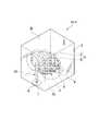
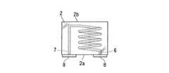
図1は、本発明の第一実施形態にかかる電子回路チップ配線基板の電子回路チップ1A(1)を示す斜視図である。
この電子回路チップ1A(1)は、基体2とこの基体2の内部に配された回路10とを備えた電子回路チップであって、回路10の一方の端部(第1端部)6と他方の端部(第2端部)7はそれぞれ、基体2の特定面(第1面2a)に露呈される。回路10は、螺旋状のインダクタ9を含む。基体2は、ガラス又は半導体からなる。Preferred embodiments of the present invention will be described below with reference to the drawings.
<Electronic circuit chip>
FIG. 1 is a perspective view showing an
The
基体2は、石英ガラス等のガラス又はシリコン等の半導体からなる単一層の基体である。ここで、「単一層の基体」とは、複数の基板を張り合わせた多層構造の基体とは区別される基体を表す。 The
基体2は、ガラス又は半導体からなるため、半導体デバイスに実装される場合、これらの線膨張係数差は小さい。このため、電子回路チップ1A(1)と半導体デバイスとを、半田等を用いて接続する際に、位置ズレが生じず、精度の高い接続が可能となる。
基体2の材料としては、特に、絶縁性を有するガラスが好ましい。この場合、基体内部に形成される微細孔3の内壁面に絶縁層を形成せずに、導体4を充填又は成膜することができる。さらに、回路10において、浮遊容量成分の存在等による高速伝送の阻害要因がない等の利点がある。
基体2の厚さは、適宜設定することができ、例えば約150μm〜1mmの範囲に設定することができる。Since the
As a material for the
The thickness of the
回路10は、基体2内部に形成された微細孔3に、導体4が成膜又は充填されて形成される。
導体4としては、例えばCu(銅)、Ag(銀)、Au(金)、及びAl(アルミ)等の金属や金錫(Au−Sn)等の合金が用いられる。微細孔3に導体4を成膜又は充填する方法としては、溶融金属充填法、めっき法、超臨界流体を利用した成膜法等が適宜用いられる。図9に示すように、溶融金属充填法やめっき法であれば、微細孔3の内部に、隙間なく導体4を充填することができる。一方、図10に示すように、めっき法や超臨界流体を利用した成膜法であれば、薄膜状の導体4を微細孔3の内壁に沿って形成することができる。
また、導体4として、微細孔3に充填又は成膜することができる材料であれば、展性(延性)に乏しいために線材になり難い導電性物質を使用することもできる。The
As the
In addition, as long as the
インダクタ9は、仮想の、円柱(円筒)、楕円柱、又は円環(トーラス)に巻きつけたような滑らかな螺旋状であることが好ましい。ここで、前記円環に巻きつけたような滑らかな螺旋状のインダクタの形状とは、いわゆるトロイダルコイルにおけるコイル形状を意味する。 The
図2に示す電子回路チップ1A−1(1)において、インダクタ9を構成する導体4は、仮想の円柱(円筒)に巻きつけたような滑らかな螺旋状をなしている。
図3に示す電子回路チップ1A−2(1)において、インダクタ9を構成する導体4は、仮想の楕円柱に巻きつけたような滑らかな螺旋状をなしている。
図4に示す電子回路チップ1A−3(1)において、インダクタ9を構成する導体4は、仮想の円環に巻きつけたような滑らかな螺旋状をなしている。In the
In the
In the
インダクタ9を、上記のような滑らかな螺旋状とすることによって、高周波等の伝送損失を低減して、効率よく磁界を発生させることができる。
また、インダクタ9は、継ぎ目(繋ぎ目)の無い、連続的な曲線によって構成されることが好ましい。この場合、インダクタが、複数の配線を繋ぎ合わせた不連続な曲線(一部に直線を有するような曲線)から構成される場合と比べて、高周波の伝送損失が低減され、且つ、継ぎ目に生じる接合不良や剥離不良が防止される。By making the
Moreover, it is preferable that the
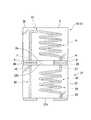
回路10の形状やインダクタ9の形状(巻き数や螺旋径の大きさ)は特に制限されず、用途や基体の形状に合わせて所望の形状に形成される。例えば、図5に示す本発明の第二実施形態に係る電子回路チップ1B(1)における回路15のような形状であってもよい。 The shape of the
回路10の一方の端部6および他方の端部7には、外部電極端子8が設けられていることが好ましい。これにより、電子回路チップ1A(1)を実装基板(不図示)に電気的に接合したり、電子回路チップ1A(1)と他の電子回路チップとを電気的に接合することが容易になる。
外部電極端子8の材質は、導電性材料からなる材質であれば特に制限されず、アルミニウム、銅からなる金属板(金属膜)やはんだバンプ等が適用できる。An
The material of the
回路10の一方の端部6および他方の端部7は、基体2の特定面に露呈している。一方の端部6および他方の端部7が、同一面に露呈されており、回路10を備える電子回路チップ1A(1)を、プリント回路基板等の平坦な面上に装着することができる。 One
図1及び図5では、一方の端部6,16および他方の端部7,17の両方が基体2の一の面2aに露呈されているが、必ずしも両方の端部が同一面に露呈されていなくてもよい。
例えば、図6に示す第二の電子回路チップ21(第三実施形態)のように、回路30の一方の端部(第1端部)26は基体22の一の面(第1面)22aに露呈し、回路30の他方の端部(第2端部)27は基体22の他の面(第2面)22bに露呈していてもよい。一の面22aと他の面22bとは、基体22の互いに反対側に位置する二つの面である。In FIG. 1 and FIG. 5, both one
For example, as in the second electronic circuit chip 21 (third embodiment) shown in FIG. 6, one end (first end) 26 of the
このように、一方の端部26と他方の端部27とが基体22の反対側に位置する二つの面にそれぞれ設けられることによって、第二の電子回路チップ21の上に、別の電子デバイスを積み重ねて電気的に接続することが可能となる。 Thus, by providing the one
図6は、第二の電子回路チップ21の上に第一の電子回路チップ1A(1)を積み重ねて備えた複合型電子回路チップの一例である。
第二の電子回路チップ21における回路30の他方の端部27に設けられた外部電極端子28と、第一の電子回路チップ1における回路10の一方の端部6に設けられた外部電極端子8と、が電気的に接合されている。同様に、第二の電子回路チップ21における回路40の一方の端部46に設けられた外部電極端子48と、第一の電子回路チップ1における回路10の他方の端部7に設けられた外部電極端子8と、が電気的に接合されている。FIG. 6 is an example of a composite electronic circuit chip provided with the first
The external electrode terminal 28 provided at the
第二の電子回路チップ21の回路30には、インダクタ29が形成されている。このインダクタ29は、第一の電子回路チップ1の回路10に形成されたインダクタ9と、同様である。 An
この複合型電子回路チップでは、第二の電子回路チップ21内のインダクタ29と、第一の電子回路チップ1のインダクタ9とが直列に配されて、連動して機能する。すなわち、両方のインダクタが発生する磁場は互いに影響を与え合い、連動して機能するため、単一のインダクタとして見なすことができる。 In this composite electronic circuit chip, the
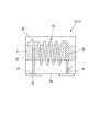
図1,図5,図6で例示した電子回路チップ1A,1B,21に形成されたインダクタ9,19,29は、いずれも空芯インダクタとして描いている。しかし、これらのインダクタは、コアインダクタとすることもできる。基体において、コアとなる領域に設けたキャビティに、フェライト等の磁性体を配することによって、コアインダクタとすることができる。 The
例えば、図7に示す第四実施形態である電子回路チップ1C(1)が挙げられる。この電子回路チップ1C(1)において、電子回路チップ1B(1)と同じ構成には、同じ符号を付した。
電子回路チップ1C(1)は、インダクタ19の芯部に磁性体からなるコア14を備えている。
前記磁性体の材料としては、コアコイルに通常使用される材料であれば特に制限されず、例えば酸化鉄、Mn、Co、Ni、Cu、Zn等が挙げられる。
コア14の形状は、棒状、E字型、鼓型等が挙げられる。このうち、製造が容易である観点から、棒状が好ましい。コアが棒状(円柱形)である場合、その直径は、インダクタの内径(=1)に対して0.2〜0.9とすればよい。For example, an
The
The material of the magnetic body is not particularly limited as long as it is a material usually used for the core coil, and examples thereof include iron oxide, Mn, Co, Ni, Cu, and Zn.
Examples of the shape of the core 14 include a rod shape, an E shape, and a drum shape. Of these, a rod shape is preferable from the viewpoint of easy production. When the core is rod-shaped (cylindrical), the diameter may be 0.2 to 0.9 with respect to the inner diameter (= 1) of the inductor.
<電子回路チップの製造方法>
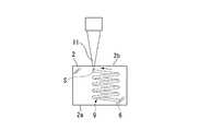
次に、本発明の一実施形態に係る電子回路チップの製造方法として、電子回路チップ1A(1)を製造する方法を図8A〜図8Gに示す。
ここで、図8A〜図8Gは、電子回路チップ1A(1)を製造する基体2の正面図である。<Electronic circuit chip manufacturing method>
Next, as a method for manufacturing an electronic circuit chip according to an embodiment of the present invention, a method for manufacturing the
Here, FIGS. 8A to 8G are front views of the
[工程A]
まず、図8Aに示すように、ガラス又は半導体からなる基体2にレーザー光11を照射して、基体2内にガラス又は半導体が改質されてなる改質部12を形成する。この改質部12は、回路10が配される領域に形成される。[Process A]
First, as shown in FIG. 8A, the
基体2の材料は、ガラス基板又はシリコン等の半導体基板が好ましい。
これらの基板を使用した場合の製造方法としては、例えば300mm径のガラス基板又は半導体基板に、改質部12を複数形成して、複数の回路10を備えたガラス基板又は半導体基板を得る。その後、この基板から個々の電子回路チップをダイシング等によって切り出して製造する方法が、製造効率の観点から好ましい。The material of the
As a manufacturing method when these substrates are used, for example, a plurality of modified
基体2の他の面(第2面)2b側からレーザー光11を照射して、基体2内に焦点Sを結ぶ。焦点Sが結ばれた位置で、基体2の材料が改質される。回路10の一方の端部6となる位置から、インダクタ9となる領域に順に焦点Sを走査して改質部12を形成する(図8A及び図8B)。 The
つづいて、回路10の他方の端部7となる位置から、基体2の他の面2bに向けて焦点Sを走査する。次に、基体2の他の面2bと平行に焦点Sを走査して、先に形成した改質部12と継ぎ目が無いように滑らかに連結した改質部12を形成する(図8C及び図8D)。これによって、回路10となる全領域に改質部12が形成される。 Subsequently, the focal point S is scanned from the position that becomes the
レーザー光11の光源としては、例えばフェムト秒レーザーを挙げることができる。このレーザー光11を照射することによって、例えば、径が数μm〜数十μmである改質部12を形成することができる。また、基体2内部におけるレーザー光11の焦点Sを結ぶ位置を制御することにより、所望の形状を有する改質部12を形成することができる。 Examples of the light source of the
ここでは、レーザー光11を基体2の他の面2b側から照射する場合を示したが、異なる面から照射してもよい。
ただし、一般に、改質された部分のレーザーの透過率は、改質されていない部分のレーザーの透過率とは異なるため、改質された部分を透過させたレーザー光の焦点位置を制御することは通常困難である。したがって、レーザー照射する側の面から見て、奥に位置する領域について先に改質部を形成することが望ましい。Here, the case where the
However, in general, the laser transmittance of the modified part is different from the laser transmittance of the unmodified part, so the focal position of the laser beam that has passed through the modified part should be controlled. Is usually difficult. Therefore, it is desirable to form the modified portion first in the region located behind as viewed from the surface on the laser irradiation side.
[工程B]
改質部12を形成した基体2をエッチング液(薬液)に浸漬して、ウェットエッチングすることによって、改質部12を基体2から除去する。その結果、改質部12が存在した領域に、微細孔3が形成される(図8E)。本実施形態では、基体2の材料としてガラスを用い、エッチング液としてフッ酸(HF)の10質量%溶液を主成分とする溶液を用いた。[Process B]
The modified
このエッチングは、基体2の改質されていない部分に比べて、改質部12が非常に速くエッチングされる現象を利用する。この結果として、改質部12の形状に応じた微細孔3を形成することができる。
前記エッチング液は、特に限定されず、例えばフッ酸(HF)を主成分とする溶液、フッ酸に硝酸等を適量添加したフッ硝酸系の混酸等を用いることができる。また、基体2の材料に応じて、他の薬液を用いることもできる。This etching utilizes the phenomenon that the modified
The etching solution is not particularly limited, and for example, a solution containing hydrofluoric acid (HF) as a main component, or a hydrofluoric acid-based mixed acid obtained by adding an appropriate amount of nitric acid or the like to hydrofluoric acid can be used. Also, other chemicals can be used depending on the material of the
[工程C]
微細孔3が形成された基体2において、この微細孔3に導体(導電性物質)4を充填または成膜して、回路10を形成する。この導体4としては、例えば金錫(Au−Sn)、銅(Cu)等が挙げられる。この導体4の充填または成膜方法としては、溶融金属充填法、めっき法など、適宜用いることができる。図9に示すように、溶融金属充填法やめっき法であれば、微細孔3の内部に、隙間なく導体4を充填することができる。一方、図10に示すように、めっき法や超臨界流体を利用した成膜法であれば、薄膜状の導体4を微細孔3の内壁に沿って形成することができる。[Process C]
In the
以上の工程A〜Cにより、図1に示した電子回路チップ1が得られる。
さらに所望に応じて、一方の端部6および他方の端部7上に外部電極端子8を形成してもよい。外部電極端子8の形成方法は、めっき法、スパッタ法など、適宜用いることができる。Through the above steps A to C, the
Furthermore, an
また、図7に示した電子回路チップ1C(1)のように、コア14を備える電子回路チップを製造する方法としては、次の方法が挙げられる。
例えば、前述の工程Aにおいて基体2のコア14となる領域に改質部を形成し、続く工程Bにおいてこの改質部をエッチングによって除去して、形成された貫通孔に磁性体を導入する方法が挙げられる。この方法によれば、円柱、楕円、又は円環の一部を切り取った形状など、所望の形状でコア14を包含する貫通孔を形成することができる。
また、基体2に前記貫通孔を形成する他の方法としては、微小ドリルを使用する方法、基体2の表面にレジストマスクを設けてエッチングする方法、等が挙げられる。
基体2に形成した貫通孔に磁性体を導入する方法としては、例えば、棒状の磁性体を嵌め込む方法、スパッタリング法やめっき法によって磁性体を成膜又は充填する方法、磁性体を含む樹脂ペーストを印刷法によって充填する方法等が挙げられる。Further, as a method of manufacturing an electronic circuit chip including the core 14 like the
For example, a method of forming a modified portion in a region to be the
Other methods for forming the through hole in the
Examples of methods for introducing a magnetic substance into the through-hole formed in the
基体2にコア14を備える場合、回路10を先に形成しても良いし、コア14を先に形成しても良い。 When the
本発明の電子回路チップ1および電子回路チップ1の製造方法は、ICや電子部品の製造に広く利用することができる。 The
1,1A,1A−1,1A−2,1A−3,1B 電子回路チップ(第一の電子回路チップ)
2 基体
2a 基体の一の面(第1面)
2b 基体の他の面(第2面)
3 微細孔
4 導体
5 回路の配線
6 一方の端部(第1端部)
7 他方の端部(第2端部)
8 外部電極端子
9 インダクタ
10 回路
11 レーザー光
12 改質部
14 コア
15 回路
16 一方の端部(第1端部)
17 他方の端部(第2端部)
18 外部電極端子
19 インダクタ
S 焦点
21 第二の電子回路チップ
22 基体
22a 基体の一の面(第1面)
22b 基体の他の面(第2面)
26 一方の端部(第1端部)
27 他方の端部(第2端部)
28 外部電極端子
29 インダクタ
30 回路
40 回路
46 一方の端部(第1端部)
47 他方の端部(第2端部)
48 外部電極端子1, 1A, 1A-1, 1A-2, 1A-3, 1B Electronic circuit chip (first electronic circuit chip)
2
2b Other side of substrate (second side)
3
7 The other end (second end)
8
17 Other end (second end)
18
22b Other side of substrate (second side)
26 One end (first end)
27 The other end (second end)
28
47 The other end (second end)
48 External electrode terminal
Claims (9)
Translated fromJapanese前記基体の内部に配され、第1端部と第2端部がそれぞれ前記基体の特定面に露呈され、螺旋状のインダクタを含む回路と;
を備えた電子回路チップ。A substrate made of glass or semiconductor;
A circuit that is disposed inside the base, the first end and the second end are exposed to a specific surface of the base, respectively, and includes a spiral inductor;
Electronic circuit chip equipped with.
前記第1端部が、前記第1面に設けられ、
前記第2端部が、前記第2面に設けられている
ことを特徴とする請求項1〜5のいずれか一項に記載の電子回路チップ。The base includes a first surface and a second surface located on the opposite side of the first surface;
The first end is provided on the first surface;
The electronic circuit chip according to claim 1, wherein the second end portion is provided on the second surface.
前記改質部が形成された前記基体に対してエッチング処理を行い、前記改質部を除去して螺旋状の微細孔を形成し;
前記微細孔に導体を充填又は成膜する;
ことを特徴とする電子回路チップの製造方法。Irradiating the inside of a substrate made of glass or semiconductor with laser light, and scanning the focal point where the laser light is condensed to form a helical modified portion;
An etching process is performed on the substrate on which the modified portion is formed, and the modified portion is removed to form a spiral micropore;
Filling the micropores with a conductor or forming a film;
An electronic circuit chip manufacturing method characterized by the above.
Applications Claiming Priority (3)
| Application Number | Priority Date | Filing Date | Title |
|---|---|---|---|
| JP2010176472 | 2010-08-05 | ||
| JP2010176472 | 2010-08-05 | ||
| PCT/JP2011/066914WO2012017857A1 (en) | 2010-08-05 | 2011-07-26 | Electronic circuit chip and method of manufacturing electronic circuit chip |
Publications (1)
| Publication Number | Publication Date |
|---|---|
| JPWO2012017857A1true JPWO2012017857A1 (en) | 2013-10-03 |
Family
ID=45559360
Family Applications (1)
| Application Number | Title | Priority Date | Filing Date |
|---|---|---|---|
| JP2012527667APendingJPWO2012017857A1 (en) | 2010-08-05 | 2011-07-26 | Electronic circuit chip and method for manufacturing electronic circuit chip |
Country Status (5)
| Country | Link |
|---|---|
| US (1) | US20130143381A1 (en) |
| EP (1) | EP2584571A1 (en) |
| JP (1) | JPWO2012017857A1 (en) |
| CN (1) | CN103038839A (en) |
| WO (1) | WO2012017857A1 (en) |
Families Citing this family (42)
| Publication number | Priority date | Publication date | Assignee | Title |
|---|---|---|---|---|
| US9721715B2 (en)* | 2009-01-22 | 2017-08-01 | 2Sentient Inc. | Solid state components having an air core |
| WO2012014723A1 (en)* | 2010-07-26 | 2012-02-02 | 浜松ホトニクス株式会社 | Method for manufacturing light-absorbing substrate and method for manufacturing die for manufacturing light-absorbing substrate |
| JP5693074B2 (en)* | 2010-07-26 | 2015-04-01 | 浜松ホトニクス株式会社 | Laser processing method |
| WO2012014720A1 (en)* | 2010-07-26 | 2012-02-02 | 浜松ホトニクス株式会社 | Laser processing method |
| US8803648B2 (en) | 2012-05-03 | 2014-08-12 | Qualcomm Mems Technologies, Inc. | Three-dimensional multilayer solenoid transformer |
| US20140104284A1 (en)* | 2012-10-16 | 2014-04-17 | Qualcomm Mems Technologies, Inc. | Through substrate via inductors |
| US20140247269A1 (en)* | 2013-03-04 | 2014-09-04 | Qualcomm Mems Technologies, Inc. | High density, low loss 3-d through-glass inductor with magnetic core |
| US9866197B2 (en) | 2013-06-06 | 2018-01-09 | Qorvo Us, Inc. | Tunable RF filter based RF communications system |
| US12224096B2 (en) | 2013-03-15 | 2025-02-11 | Qorvo Us, Inc. | Advanced 3D inductor structures with confined magnetic field |
| US9755671B2 (en) | 2013-08-01 | 2017-09-05 | Qorvo Us, Inc. | VSWR detector for a tunable filter structure |
| US9705478B2 (en) | 2013-08-01 | 2017-07-11 | Qorvo Us, Inc. | Weakly coupled tunable RF receiver architecture |
| US9780756B2 (en) | 2013-08-01 | 2017-10-03 | Qorvo Us, Inc. | Calibration for a tunable RF filter structure |
| US9685928B2 (en) | 2013-08-01 | 2017-06-20 | Qorvo Us, Inc. | Interference rejection RF filters |
| US9391565B2 (en) | 2013-03-15 | 2016-07-12 | TriQuint International PTE, Ltd. | Amplifier phase distortion correction based on amplitude distortion measurement |
| US9628045B2 (en) | 2013-08-01 | 2017-04-18 | Qorvo Us, Inc. | Cooperative tunable RF filters |
| US9899133B2 (en)* | 2013-08-01 | 2018-02-20 | Qorvo Us, Inc. | Advanced 3D inductor structures with confined magnetic field |
| US9774311B2 (en) | 2013-03-15 | 2017-09-26 | Qorvo Us, Inc. | Filtering characteristic adjustments of weakly coupled tunable RF filters |
| US9825656B2 (en) | 2013-08-01 | 2017-11-21 | Qorvo Us, Inc. | Weakly coupled tunable RF transmitter architecture |
| US9871499B2 (en) | 2013-03-15 | 2018-01-16 | Qorvo Us, Inc. | Multi-band impedance tuners using weakly-coupled LC resonators |
| US9859863B2 (en) | 2013-03-15 | 2018-01-02 | Qorvo Us, Inc. | RF filter structure for antenna diversity and beam forming |
| US9800282B2 (en) | 2013-06-06 | 2017-10-24 | Qorvo Us, Inc. | Passive voltage-gain network |
| US9705542B2 (en) | 2013-06-06 | 2017-07-11 | Qorvo Us, Inc. | Reconfigurable RF filter |
| US9966981B2 (en) | 2013-06-06 | 2018-05-08 | Qorvo Us, Inc. | Passive acoustic resonator based RF receiver |
| US9780817B2 (en) | 2013-06-06 | 2017-10-03 | Qorvo Us, Inc. | RX shunt switching element-based RF front-end circuit |
| JP6309735B2 (en)* | 2013-10-07 | 2018-04-11 | 日本特殊陶業株式会社 | Wiring board and manufacturing method thereof |
| CN103915239A (en)* | 2014-04-02 | 2014-07-09 | 湖州科富电子科技有限公司 | Novel magnetic core |
| EP3140838B1 (en)* | 2014-05-05 | 2021-08-25 | 3D Glass Solutions, Inc. | Inductive device in a photo-definable glass structure |
| US9129843B1 (en)* | 2014-06-12 | 2015-09-08 | Globalfoundries Inc. | Integrated inductor |
| CN104347240B (en)* | 2014-10-09 | 2016-12-07 | 东莞建冠塑胶电子有限公司 | Thin induction coil |
| US10796835B2 (en) | 2015-08-24 | 2020-10-06 | Qorvo Us, Inc. | Stacked laminate inductors for high module volume utilization and performance-cost-size-processing-time tradeoff |
| US12165809B2 (en) | 2016-02-25 | 2024-12-10 | 3D Glass Solutions, Inc. | 3D capacitor and capacitor array fabricating photoactive substrates |
| US10692645B2 (en) | 2016-03-23 | 2020-06-23 | Qorvo Us, Inc. | Coupled inductor structures |
| US11139238B2 (en) | 2016-12-07 | 2021-10-05 | Qorvo Us, Inc. | High Q factor inductor structure |
| WO2018162385A1 (en)* | 2017-03-06 | 2018-09-13 | Lpkf Laser & Electronics Ag | Method for producing at least one recess in a material by means of electromagnetic radiation and subsequent etching process |
| JP6895062B2 (en)* | 2017-05-01 | 2021-06-30 | 日本電信電話株式会社 | Inductor |
| US10172237B1 (en)* | 2017-08-28 | 2019-01-01 | Osram Sylvania Inc. | Space-efficient PCB-based inductor |
| JP7008824B2 (en) | 2017-12-15 | 2022-01-25 | スリーディー グラス ソリューションズ,インク | Connection transmission line resonant RF filter |
| WO2020208750A1 (en) | 2019-04-10 | 2020-10-15 | オリンパス株式会社 | Method for manufacturing imaging device, imaging device, and endoscope |
| KR20220164800A (en) | 2020-04-17 | 2022-12-13 | 3디 글래스 솔루션즈 인코포레이티드 | broadband inductor |
| CN111885819B (en)* | 2020-07-31 | 2022-03-29 | 生益电子股份有限公司 | Circuit board inner layer interconnect structure |
| JP2022139125A (en)* | 2021-03-11 | 2022-09-26 | Tdk株式会社 | Coil component |
| JP2022139129A (en)* | 2021-03-11 | 2022-09-26 | Tdk株式会社 | Coil component and method of manufacturing the same |
Citations (8)
| Publication number | Priority date | Publication date | Assignee | Title |
|---|---|---|---|---|
| JPS53120173A (en)* | 1977-03-28 | 1978-10-20 | Mitsubishi Electric Corp | Inductor |
| JPS5818307U (en)* | 1981-07-24 | 1983-02-04 | 東光株式会社 | molded coil |
| JPS5972709U (en)* | 1982-11-05 | 1984-05-17 | 株式会社村田製作所 | chip inductor |
| JPH01266702A (en)* | 1988-04-18 | 1989-10-24 | Fujitsu Ltd | inductor structure |
| JPH09129458A (en)* | 1995-10-30 | 1997-05-16 | Matsushita Electric Ind Co Ltd | Coil parts |
| JP2004309204A (en)* | 2003-04-03 | 2004-11-04 | Cluster Technology Co Ltd | High frequency heating chips and equipment |
| JP2006303360A (en)* | 2005-04-25 | 2006-11-02 | Fujikura Ltd | Through wiring substrate, composite substrate, and electronic device |
| JP2009033152A (en)* | 2007-07-03 | 2009-02-12 | Ngk Insulators Ltd | Ceramic structure, and manufacturing method thereof |
Family Cites Families (7)
| Publication number | Priority date | Publication date | Assignee | Title |
|---|---|---|---|---|
| JPH04373112A (en)* | 1991-06-21 | 1992-12-25 | Tokin Corp | Inductor and manufacturing method thereof |
| JPH04373106A (en)* | 1991-06-21 | 1992-12-25 | Tokin Corp | Inductor and manufacturing method thereof |
| JPH05283238A (en)* | 1992-03-31 | 1993-10-29 | Sony Corp | Transformer |
| US6531945B1 (en)* | 2000-03-10 | 2003-03-11 | Micron Technology, Inc. | Integrated circuit inductor with a magnetic core |
| US6880232B2 (en)* | 2001-09-26 | 2005-04-19 | Intel Corporation | Method of making an electrical inductor using a sacrificial electrode |
| JP2003100517A (en) | 2001-09-27 | 2003-04-04 | Fdk Corp | Multilayer chip inductor and method of manufacturing the same |
| JP5054445B2 (en)* | 2007-06-26 | 2012-10-24 | スミダコーポレーション株式会社 | Coil parts |
- 2011
- 2011-07-26JPJP2012527667Apatent/JPWO2012017857A1/enactivePending
- 2011-07-26CNCN2011800372507Apatent/CN103038839A/enactivePending
- 2011-07-26EPEP11814485.6Apatent/EP2584571A1/ennot_activeWithdrawn
- 2011-07-26WOPCT/JP2011/066914patent/WO2012017857A1/enactiveApplication Filing
- 2013
- 2013-01-30USUS13/754,081patent/US20130143381A1/ennot_activeAbandoned
Patent Citations (8)
| Publication number | Priority date | Publication date | Assignee | Title |
|---|---|---|---|---|
| JPS53120173A (en)* | 1977-03-28 | 1978-10-20 | Mitsubishi Electric Corp | Inductor |
| JPS5818307U (en)* | 1981-07-24 | 1983-02-04 | 東光株式会社 | molded coil |
| JPS5972709U (en)* | 1982-11-05 | 1984-05-17 | 株式会社村田製作所 | chip inductor |
| JPH01266702A (en)* | 1988-04-18 | 1989-10-24 | Fujitsu Ltd | inductor structure |
| JPH09129458A (en)* | 1995-10-30 | 1997-05-16 | Matsushita Electric Ind Co Ltd | Coil parts |
| JP2004309204A (en)* | 2003-04-03 | 2004-11-04 | Cluster Technology Co Ltd | High frequency heating chips and equipment |
| JP2006303360A (en)* | 2005-04-25 | 2006-11-02 | Fujikura Ltd | Through wiring substrate, composite substrate, and electronic device |
| JP2009033152A (en)* | 2007-07-03 | 2009-02-12 | Ngk Insulators Ltd | Ceramic structure, and manufacturing method thereof |
Also Published As
| Publication number | Publication date |
|---|---|
| EP2584571A1 (en) | 2013-04-24 |
| US20130143381A1 (en) | 2013-06-06 |
| CN103038839A (en) | 2013-04-10 |
| WO2012017857A1 (en) | 2012-02-09 |
Similar Documents
| Publication | Publication Date | Title |
|---|---|---|
| JPWO2012017857A1 (en) | Electronic circuit chip and method for manufacturing electronic circuit chip | |
| JP7287185B2 (en) | Electronic component, electronic component mounting substrate, and method for manufacturing electronic component | |
| US12033789B2 (en) | Inductor component and inductor component embedded substrate | |
| JP7243569B2 (en) | Inductor components and substrates with built-in inductor components | |
| CN104011812B (en) | Coil component | |
| JP7306219B2 (en) | Inductor array components and substrates with built-in inductor array components | |
| JP6361082B2 (en) | Coil component and manufacturing method thereof | |
| JP2019134141A (en) | Inductor component and manufacturing method thereof | |
| JP6230972B2 (en) | Chip electronic component and manufacturing method thereof | |
| KR102016490B1 (en) | Coil Component | |
| JP5711572B2 (en) | Circuit board for isolator, isolator and manufacturing method thereof | |
| JP2018113299A (en) | Inductor component | |
| KR20150081802A (en) | Chip electronic component and manufacturing method thereof | |
| CN106205974A (en) | Coil Electronic Assemblies | |
| JP2017034228A (en) | Magnetic powder and coil electronic component containing the same | |
| JP2005327876A (en) | Coil component and its manufacturing method | |
| JP2016051765A (en) | Inductor component | |
| JPWO2017131017A1 (en) | Inductor component and manufacturing method thereof | |
| JP2013135232A (en) | Method of manufacturing inductor | |
| KR102105397B1 (en) | Chip electronic component and board having the same mounted thereon | |
| JP2016195246A (en) | Coil electronic component and method for manufacturing the same | |
| CN119049845A (en) | Inductance component | |
| US20240055176A1 (en) | Inductor and body part for inductor | |
| JP6521104B2 (en) | Inductor component and method of manufacturing the same | |
| JP7092099B2 (en) | Electronic components and their manufacturing methods |
Legal Events
| Date | Code | Title | Description |
|---|---|---|---|
| A131 | Notification of reasons for refusal | Free format text:JAPANESE INTERMEDIATE CODE: A131 Effective date:20130702 | |
| A521 | Request for written amendment filed | Free format text:JAPANESE INTERMEDIATE CODE: A523 Effective date:20130828 | |
| A02 | Decision of refusal | Free format text:JAPANESE INTERMEDIATE CODE: A02 Effective date:20140304 |