JPWO2011001715A1 - Oxide semiconductor, thin film transistor array substrate, manufacturing method thereof, and display device - Google Patents
Oxide semiconductor, thin film transistor array substrate, manufacturing method thereof, and display deviceDownload PDFInfo
- Publication number
- JPWO2011001715A1 JPWO2011001715A1JP2011520808AJP2011520808AJPWO2011001715A1JP WO2011001715 A1JPWO2011001715 A1JP WO2011001715A1JP 2011520808 AJP2011520808 AJP 2011520808AJP 2011520808 AJP2011520808 AJP 2011520808AJP WO2011001715 A1JPWO2011001715 A1JP WO2011001715A1
- Authority
- JP
- Japan
- Prior art keywords
- thin film
- film transistor
- oxide semiconductor
- array substrate
- layer
- Prior art date
- Legal status (The legal status is an assumption and is not a legal conclusion. Google has not performed a legal analysis and makes no representation as to the accuracy of the status listed.)
- Pending
Links
Images


Classifications
- H—ELECTRICITY
- H10—SEMICONDUCTOR DEVICES; ELECTRIC SOLID-STATE DEVICES NOT OTHERWISE PROVIDED FOR
- H10D—INORGANIC ELECTRIC SEMICONDUCTOR DEVICES
- H10D62/00—Semiconductor bodies, or regions thereof, of devices having potential barriers
- H10D62/80—Semiconductor bodies, or regions thereof, of devices having potential barriers characterised by the materials
- H10D62/86—Semiconductor bodies, or regions thereof, of devices having potential barriers characterised by the materials being Group II-VI materials, e.g. ZnO
- H—ELECTRICITY
- H10—SEMICONDUCTOR DEVICES; ELECTRIC SOLID-STATE DEVICES NOT OTHERWISE PROVIDED FOR
- H10D—INORGANIC ELECTRIC SEMICONDUCTOR DEVICES
- H10D30/00—Field-effect transistors [FET]
- H10D30/01—Manufacture or treatment
- H10D30/021—Manufacture or treatment of FETs having insulated gates [IGFET]
- H10D30/031—Manufacture or treatment of FETs having insulated gates [IGFET] of thin-film transistors [TFT]
- H—ELECTRICITY
- H10—SEMICONDUCTOR DEVICES; ELECTRIC SOLID-STATE DEVICES NOT OTHERWISE PROVIDED FOR
- H10D—INORGANIC ELECTRIC SEMICONDUCTOR DEVICES
- H10D30/00—Field-effect transistors [FET]
- H10D30/60—Insulated-gate field-effect transistors [IGFET]
- H10D30/67—Thin-film transistors [TFT]
- H10D30/6729—Thin-film transistors [TFT] characterised by the electrodes
- H10D30/6737—Thin-film transistors [TFT] characterised by the electrodes characterised by the electrode materials
- H10D30/6739—Conductor-insulator-semiconductor electrodes
- H—ELECTRICITY
- H10—SEMICONDUCTOR DEVICES; ELECTRIC SOLID-STATE DEVICES NOT OTHERWISE PROVIDED FOR
- H10D—INORGANIC ELECTRIC SEMICONDUCTOR DEVICES
- H10D30/00—Field-effect transistors [FET]
- H10D30/60—Insulated-gate field-effect transistors [IGFET]
- H10D30/67—Thin-film transistors [TFT]
- H10D30/674—Thin-film transistors [TFT] characterised by the active materials
- H10D30/6755—Oxide semiconductors, e.g. zinc oxide, copper aluminium oxide or cadmium stannate
- H—ELECTRICITY
- H10—SEMICONDUCTOR DEVICES; ELECTRIC SOLID-STATE DEVICES NOT OTHERWISE PROVIDED FOR
- H10D—INORGANIC ELECTRIC SEMICONDUCTOR DEVICES
- H10D64/00—Electrodes of devices having potential barriers
- H10D64/60—Electrodes characterised by their materials
- H10D64/62—Electrodes ohmically coupled to a semiconductor
- H—ELECTRICITY
- H10—SEMICONDUCTOR DEVICES; ELECTRIC SOLID-STATE DEVICES NOT OTHERWISE PROVIDED FOR
- H10D—INORGANIC ELECTRIC SEMICONDUCTOR DEVICES
- H10D99/00—Subject matter not provided for in other groups of this subclass
- G—PHYSICS
- G02—OPTICS
- G02F—OPTICAL DEVICES OR ARRANGEMENTS FOR THE CONTROL OF LIGHT BY MODIFICATION OF THE OPTICAL PROPERTIES OF THE MEDIA OF THE ELEMENTS INVOLVED THEREIN; NON-LINEAR OPTICS; FREQUENCY-CHANGING OF LIGHT; OPTICAL LOGIC ELEMENTS; OPTICAL ANALOGUE/DIGITAL CONVERTERS
- G02F1/00—Devices or arrangements for the control of the intensity, colour, phase, polarisation or direction of light arriving from an independent light source, e.g. switching, gating or modulating; Non-linear optics
- G02F1/01—Devices or arrangements for the control of the intensity, colour, phase, polarisation or direction of light arriving from an independent light source, e.g. switching, gating or modulating; Non-linear optics for the control of the intensity, phase, polarisation or colour
- G02F1/13—Devices or arrangements for the control of the intensity, colour, phase, polarisation or direction of light arriving from an independent light source, e.g. switching, gating or modulating; Non-linear optics for the control of the intensity, phase, polarisation or colour based on liquid crystals, e.g. single liquid crystal display cells
- G02F1/133—Constructional arrangements; Operation of liquid crystal cells; Circuit arrangements
- G02F1/136—Liquid crystal cells structurally associated with a semi-conducting layer or substrate, e.g. cells forming part of an integrated circuit
- G02F1/1362—Active matrix addressed cells
- G02F1/1368—Active matrix addressed cells in which the switching element is a three-electrode device
- G—PHYSICS
- G02—OPTICS
- G02F—OPTICAL DEVICES OR ARRANGEMENTS FOR THE CONTROL OF LIGHT BY MODIFICATION OF THE OPTICAL PROPERTIES OF THE MEDIA OF THE ELEMENTS INVOLVED THEREIN; NON-LINEAR OPTICS; FREQUENCY-CHANGING OF LIGHT; OPTICAL LOGIC ELEMENTS; OPTICAL ANALOGUE/DIGITAL CONVERTERS
- G02F2202/00—Materials and properties
- G02F2202/10—Materials and properties semiconductor
- H—ELECTRICITY
- H01—ELECTRIC ELEMENTS
- H01L—SEMICONDUCTOR DEVICES NOT COVERED BY CLASS H10
- H01L21/00—Processes or apparatus adapted for the manufacture or treatment of semiconductor or solid state devices or of parts thereof
- H01L21/02—Manufacture or treatment of semiconductor devices or of parts thereof
- H01L21/02104—Forming layers
- H01L21/02365—Forming inorganic semiconducting materials on a substrate
- H01L21/02518—Deposited layers
- H01L21/02521—Materials
- H01L21/02551—Group 12/16 materials
- H01L21/02554—Oxides
- H—ELECTRICITY
- H01—ELECTRIC ELEMENTS
- H01L—SEMICONDUCTOR DEVICES NOT COVERED BY CLASS H10
- H01L21/00—Processes or apparatus adapted for the manufacture or treatment of semiconductor or solid state devices or of parts thereof
- H01L21/02—Manufacture or treatment of semiconductor devices or of parts thereof
- H01L21/02104—Forming layers
- H01L21/02365—Forming inorganic semiconducting materials on a substrate
- H01L21/02518—Deposited layers
- H01L21/02521—Materials
- H01L21/02565—Oxide semiconducting materials not being Group 12/16 materials, e.g. ternary compounds
- H—ELECTRICITY
- H01—ELECTRIC ELEMENTS
- H01L—SEMICONDUCTOR DEVICES NOT COVERED BY CLASS H10
- H01L21/00—Processes or apparatus adapted for the manufacture or treatment of semiconductor or solid state devices or of parts thereof
- H01L21/02—Manufacture or treatment of semiconductor devices or of parts thereof
- H01L21/02104—Forming layers
- H01L21/02365—Forming inorganic semiconducting materials on a substrate
- H01L21/02612—Formation types
- H01L21/02617—Deposition types
- H01L21/02631—Physical deposition at reduced pressure, e.g. MBE, sputtering, evaporation
Landscapes
- Thin Film Transistor (AREA)
- Liquid Crystal (AREA)
Abstract
Translated fromJapaneseDescription
Translated fromJapanese本発明は、酸化物半導体、薄膜トランジスタアレイ基板及びその製造方法、並びに、表示装置に関する。より詳しくは、薄膜トランジスタのチャネル層として好適な酸化物半導体、この酸化物半導体を用いてチャネル層を形成した薄膜トランジスタを備える薄膜トランジスタアレイ基板及びその製造方法、並びに、この薄膜トランジスタアレイ基板を備える表示装置に関するものである。The present invention relates to an oxide semiconductor, a thin film transistor array substrate, a method for manufacturing the same, and a display device. More particularly, the present invention relates to an oxide semiconductor suitable as a channel layer of a thin film transistor, a thin film transistor array substrate including a thin film transistor in which a channel layer is formed using the oxide semiconductor, a manufacturing method thereof, and a display device including the thin film transistor array substrate. It is.
酸化物半導体は、アモルファスシリコン(a−Si)等のシリコン系材料よりも高い電子移動度を有する半導体材料である。例えば、酸化物半導体を薄膜トランジスタ(TFT)のチャネル層に用いた場合には、信頼性に優れ、しかも電圧無印加時に流れる漏れ電流の低いTFTが実現できると考えられることから、酸化物半導体を用いたTFTの開発が進められている。An oxide semiconductor is a semiconductor material having higher electron mobility than a silicon-based material such as amorphous silicon (a-Si). For example, when an oxide semiconductor is used for a channel layer of a thin film transistor (TFT), it is considered that a TFT with excellent reliability and low leakage current that flows when no voltage is applied can be realized. Development of TFTs that have been in progress is ongoing.
酸化物半導体の中でもインジウム(In)、ガリウム(Ga)、亜鉛(Zn)、及び、酸素(O)を構成原子として含む4元型の酸化物半導体(以下、IGZO半導体とも称す。)は、移動度が高いだけでなく、以下のような特性を有するため、よりTFTに適していると考えられる。Among oxide semiconductors, a quaternary oxide semiconductor (hereinafter also referred to as an IGZO semiconductor) containing indium (In), gallium (Ga), zinc (Zn), and oxygen (O) as constituent atoms moves. Not only is the degree high but also has the following characteristics, it is considered more suitable for TFT.
まず、IGZO半導体は、室温〜150℃程度の比較的低い温度で成膜が可能である。上記シリコン系材料は、TFTを300℃以上の高温で成膜するため、フィルム基材を用いたフレキシブル基板のように高温雰囲気下に不適な基材には、直接にTFTを形成することができなかったが、酸化物半導体を用いることで、フレキシブル基板に直接にTFTを形成することも可能となる。また、IGZO半導体は、スパッタ装置での成膜が可能であり、簡易な工程で製造できる。First, the IGZO semiconductor can be formed at a relatively low temperature of about room temperature to about 150 ° C. Since the above-mentioned silicon-based material forms TFTs at a high temperature of 300 ° C. or higher, TFTs can be directly formed on a substrate that is not suitable in a high-temperature atmosphere, such as a flexible substrate using a film substrate. However, by using an oxide semiconductor, a TFT can be formed directly on a flexible substrate. Further, the IGZO semiconductor can be formed by a sputtering apparatus and can be manufactured by a simple process.
更に、IGZO半導体にて形成された薄膜は、可視光を透過させることができ、透明性にも優れている。そのため、酸化インジウム錫(Indium Tin Oxide:ITO)等が用いられている透明電極の用途にも適用できる。Furthermore, a thin film formed of an IGZO semiconductor can transmit visible light and has excellent transparency. Therefore, it is applicable also to the use of the transparent electrode in which indium tin oxide (Indium Tin Oxide: ITO) etc. are used.
ここで、IGZO半導体の特性は、構成原子の組成によって変化する。そこで、特許文献1には、TFTのチャネル層として好適な酸化物半導体について構成原子の好ましい組成を示す相図が開示されており、特許文献2には、TFT等の透明電極として好適な酸化物半導体について構成原子の好ましい組成が開示されている。Here, the characteristics of the IGZO semiconductor vary depending on the composition of the constituent atoms. Therefore,
上記特許文献1、2に記載された組成を有するIGZO半導体(酸化物半導体)は、IGZO半導体を用いて形成した半導体層そのものは、移動度や透明性等の点で優れている。しかしながら、IGZO半導体を、例えば、半導体層をTFTのチャネル層として適用したときには、安定して高いトランジスタ特性を維持することができないことがある。In the IGZO semiconductor (oxide semiconductor) having the composition described in
これは、以下のような理由によるものと考えられる。TFTは、信号電極、ドレイン電極、ゲート電極の3端子で構成され、信号電極とドレイン電極との間に設けられたチャネル層と呼ばれる領域に電流を流して、ゲート電極に加えた電圧で電流を制御してオン/オフ動作を行うものである。IGZO半導体はチャネル層を構成するが、チャネル層の形成後には、信号電極、ドレイン電極の形成が行われる。更に、TFTを保護するための保護層や、TFTが形成された基板の表面を平坦化するための層間絶縁膜も形成される。This is considered to be due to the following reasons. A TFT is composed of three terminals: a signal electrode, a drain electrode, and a gate electrode. A current is passed through a region called a channel layer provided between the signal electrode and the drain electrode, and the current is applied by a voltage applied to the gate electrode. It is controlled to perform an on / off operation. The IGZO semiconductor constitutes a channel layer. After the channel layer is formed, a signal electrode and a drain electrode are formed. Further, a protective layer for protecting the TFT and an interlayer insulating film for planarizing the surface of the substrate on which the TFT is formed are also formed.
IGZO半導体は、上記のように比較的低温で成膜できるが、電極、保護層、層間絶縁膜等の形成には、IGZO半導体の成膜温度よりも高い温度がかかり、特に、保護層、層間絶縁膜の形成には200℃以上の高い温度がかかることがある。Although the IGZO semiconductor can be formed at a relatively low temperature as described above, the electrode, the protective layer, the interlayer insulating film, etc. are formed at a temperature higher than the film forming temperature of the IGZO semiconductor. The formation of the insulating film may take a high temperature of 200 ° C. or higher.
IGZO半導体は、In、Ga、Zn、及び、Oを構成原子とするものであるが、成膜温度よりも高い温度がかかると、膜に含まれる酸素が脱離して酸素の含有量が変化する。酸素脱離が生じると、膜の原子組成は、IGZO半導体の組成(ストイキオメトリ)と大きく異なり、これにより、オフ電流の上昇、電子移動度の低下、トランジスタ特性にヒステリシスが生じる等の現象が生じて、安定したTFT特性が得られないことの一因となる。An IGZO semiconductor has In, Ga, Zn, and O as constituent atoms. However, when a temperature higher than the film forming temperature is applied, oxygen contained in the film is desorbed and the oxygen content changes. . When oxygen desorption occurs, the atomic composition of the film is significantly different from that of the IGZO semiconductor (stoichiometry), which causes phenomena such as an increase in off-current, a decrease in electron mobility, and hysteresis in transistor characteristics. As a result, it becomes a cause that a stable TFT characteristic cannot be obtained.
また、上記説明では、IGZO半導体をTFTのチャネル層として用いた場合を例に挙げて説明したが、他の分野に適用した場合においても、実際の製品となった後のIGZO半導体によって形成された膜の酸素含有量は、ストイキオメトリからのズレが大きいことがある。In the above description, the case where the IGZO semiconductor is used as the channel layer of the TFT has been described as an example. However, even when applied to other fields, the IGZO semiconductor is formed by the IGZO semiconductor after becoming an actual product. The oxygen content of the film can be significantly misaligned from stoichiometry.
なお、上記特許文献1では、酸化物半導体の酸素含有量に関する記載があるが、組成の特定は、蛍光X線分析法によって特定している。この分析法は、膜(試料)の表面は測定できるものの、厚み方向に対する分解能がないため、In、Ga、及び、Znの組成は特定できても、膜全体に含まれる酸素の含有量を正確に定量できるものではない。したがって、特許文献1に記載の酸素含有量は、製品となった後の構成原子の組成ではなく、IGZO半導体を用いて形成した膜(半導体層)の組成(ストイキオメトリ)に換算したときの値であると考えられる。In addition, in the said
また、特許文献2には、酸素欠損量についての記載があるが、酸素欠損量は陽イオンとの関連もあり一義的に決まるものでは無く、キャリア電子の量で定義されるものであり、本明細書に記載の酸素含有量のように定量的に特定できるものではない。In addition, Patent Document 2 describes the oxygen deficiency, but the oxygen deficiency is related to the cation and is not uniquely determined, but is defined by the amount of carrier electrons. It cannot be quantitatively specified like the oxygen content described in the specification.
本発明は、上記現状に鑑みてなされたものであり、安定したトランジスタ特性を有する薄膜トランジスタを実現できる酸化物半導体、この酸化物半導体で形成されたチャネル層を有する薄膜トランジスタ及びその製造方法、並びに、この薄膜トランジスタを備える表示装置を提供することを目的とするものである。The present invention has been made in view of the above situation, and an oxide semiconductor capable of realizing a thin film transistor having stable transistor characteristics, a thin film transistor having a channel layer formed of the oxide semiconductor, a manufacturing method thereof, and the An object of the present invention is to provide a display device including a thin film transistor.
本発明者らは、安定したトランジスタ特性を有する薄膜トランジスタを実現可能な酸化物半導体について種々検討したところ、In、Ga、及び、Znを含む酸化物半導体は、高い移動度を有し、信頼性(ストレス耐性)の高いトランジスタ特性が得られる材料であることにまず着目した。また、製品となったときのIGZO半導体膜の組成は、ストイキオメトリからのズレが生じており、このズレは、製造工程においてかかる熱によって生じるIGZO半導体膜からの酸素離脱によるものであることにも着目した。そして、IGZO半導体における酸素含有量を制御することにより、薄膜トランジスタのチャネル層として好適なIGZO半導体が得られ、このIGZO半導体を用いた薄膜トランジスタは、信頼性の高いトランジスタ特性を有することを見いだし、上記課題をみごとに解決することができることに想到し、本発明に到達したものである。The inventors of the present invention have studied various oxide semiconductors that can realize a thin film transistor having stable transistor characteristics. As a result, an oxide semiconductor containing In, Ga, and Zn has high mobility and reliability ( First of all, attention was paid to the fact that it is a material capable of obtaining transistor characteristics with high stress resistance. In addition, the composition of the IGZO semiconductor film when it becomes a product has a deviation from stoichiometry, and this deviation is due to oxygen desorption from the IGZO semiconductor film caused by heat in the manufacturing process. Also focused. Then, by controlling the oxygen content in the IGZO semiconductor, an IGZO semiconductor suitable as a channel layer of the thin film transistor can be obtained, and the thin film transistor using this IGZO semiconductor has been found to have highly reliable transistor characteristics. The present inventors have arrived at the present invention by conceiving that the problem can be solved brilliantly.
すなわち、本発明は、薄膜トランジスタ用の酸化物半導体であって、上記酸化物半導体は、インジウム、ガリウム、亜鉛、及び、酸素を構成原子として含み、上記酸化物半導体の酸素含有量は、ストイキオメトリの状態を原子単位で100%としたときに、87〜95%である酸化物半導体である。That is, the present invention is an oxide semiconductor for a thin film transistor, and the oxide semiconductor contains indium, gallium, zinc, and oxygen as constituent atoms, and the oxygen content of the oxide semiconductor is determined by stoichiometry. The oxide semiconductor is 87 to 95% when the state is 100% in atomic units.
インジウム、ガリウム、亜鉛、及び、酸素を構成原子として含む酸化物半導体は、移動度が高く、比較的低温での成膜が可能であり、しかもこの酸化物半導体を用いて形成した膜は、透明性に優れるものである。An oxide semiconductor containing indium, gallium, zinc, and oxygen as constituent atoms has high mobility and can be formed at a relatively low temperature. In addition, a film formed using this oxide semiconductor is transparent. It has excellent properties.
本発明においては、酸化物半導体の酸素含有量を、ストイキオメトリの状態を原子単位で100%としたときに、87〜95%の範囲とすることで、TFTのチャネル層、透明電極等に好適に使用できる。特に、TFTのチャネル層として用いた場合には、安定したトランジスタ特性を実現できる。酸素含有量が87%未満となると、TFTの電圧−電流特性が低下する傾向にある。酸素含有量が95%を超えると、IGZO膜が高抵抗化されすぎて、TFTのチャネルとして機能しにくくなる。In the present invention, when the oxygen content of the oxide semiconductor is in the range of 87 to 95% when the stoichiometric state is 100% in atomic units, the channel layer of the TFT, the transparent electrode, etc. It can be used suitably. In particular, when used as a channel layer of a TFT, stable transistor characteristics can be realized. When the oxygen content is less than 87%, the voltage-current characteristics of the TFT tend to deteriorate. If the oxygen content exceeds 95%, the resistance of the IGZO film becomes too high and it becomes difficult to function as a TFT channel.
なお、酸化物半導体の酸素含有量は、オージェ電子分光法(AES:Auger Electron Spectroscopy)分析やXPS(X−ray Photoelectron Spectroscopy)分析等の組成分析を行うことにより確認できる。Note that the oxygen content of the oxide semiconductor can be confirmed by performing compositional analysis such as Auger Electron Spectroscopy (AES) analysis or XPS (X-ray Photoelectron Spectroscopy) analysis.
また、本明細書において、「ストイキオメトリの状態」とは、金属イオンの電荷数と、酸素イオンの電荷数とが等しい状態であることを意味する。したがって、ストイキオメトリの状態にある酸化物半導体は、導電性を有するものではない。また、ストイキオメトリとは、理想状態になる膜の組成をいう。In this specification, the “stoichiometric state” means that the number of charges of metal ions is equal to the number of charges of oxygen ions. Therefore, an oxide semiconductor in a stoichiometric state does not have conductivity. Further, stoichiometry refers to the composition of a film that is in an ideal state.
本発明はまた、基板の主面上に薄膜トランジスタを有する薄膜トランジスタアレイ基板であって、上記薄膜トランジスタは、本発明の酸化物半導体で形成されたチャネル層を有する薄膜トランジスタアレイ基板でもある。上述したように、酸素含有量が制御された本発明の酸化物半導体にて形成されたチャネル層を有することで、信頼性の高い薄膜トランジスタが実現できる。The present invention is also a thin film transistor array substrate having a thin film transistor on a main surface of the substrate, and the thin film transistor is also a thin film transistor array substrate having a channel layer formed of the oxide semiconductor of the present invention. As described above, a highly reliable thin film transistor can be realized by including a channel layer formed using the oxide semiconductor of the present invention in which the oxygen content is controlled.
上記薄膜トランジスタにおいて、電子移動度は、特に限定されるものではないが、0.1cm2/Vs以上であることが好ましい。このような電子移動度を有することで、良好なトランジスタ特性が実現できる。In the above thin film transistor, the electron mobility is not particularly limited, but is preferably 0.1 cm2 / Vs or more. By having such electron mobility, good transistor characteristics can be realized.
本発明の薄膜トランジスタアレイ基板においては、上記薄膜トランジスタは、上記チャネル層を覆う保護層を更に有し、上記保護層は、酸素原子を含む材料にて形成されていることが好ましい。これにより、保護層に含まれる酸素原子によって、チャネル層の酸素含有量を上記範囲に調整できる。In the thin film transistor array substrate of the present invention, it is preferable that the thin film transistor further includes a protective layer covering the channel layer, and the protective layer is formed of a material containing oxygen atoms. Thereby, the oxygen content of a channel layer can be adjusted to the said range with the oxygen atom contained in a protective layer.
本発明はまた、本発明の薄膜トランジスタアレイ基板を備える表示装置でもある。表示装置としては、液晶表示装置、有機EL表示装置、プラズマディスプレイ表示装置、電界放出ディスプレイ表示装置等、薄膜トランジスタアレイ基板を備える各種の表示装置に適用できる。The present invention is also a display device including the thin film transistor array substrate of the present invention. The display device can be applied to various display devices including a thin film transistor array substrate, such as a liquid crystal display device, an organic EL display device, a plasma display display device, and a field emission display device.
上述のように本発明に係る薄膜トランジスタアレイ基板は、安定したトランジスタ特性を有することから、この薄膜トランジスタアレイ基板を備えた表示装置は、表示品位の良いものとなる。As described above, since the thin film transistor array substrate according to the present invention has stable transistor characteristics, the display device including the thin film transistor array substrate has good display quality.
本発明は更に、薄膜トランジスタアレイ基板の製造方法にも向けられている。すなわち、本発明は、基板の主面上に薄膜トランジスタを有する薄膜トランジスタアレイ基板の製造方法であって、上記製造方法は、基板の主面上に形成された走査配線を絶縁膜で覆う絶縁膜形成工程と、基板面を法線方向から見たときに、上記走査配線と重なる位置に酸化物半導体層を形成する半導体層形成工程と、上記酸化物半導体層上に信号配線及びドレイン電極を形成する配線及び電極形成工程と、上記信号配線及び上記ドレイン電極を覆う保護層を形成する保護層形成工程と、上記保護層を覆う層間絶縁膜を形成する層間絶縁膜形成工程とを含み、上記保護層形成工程と上記層間絶縁膜形成工程との間に、ベーク処理工程を更に含む薄膜トランジスタアレイ基板の製造方法でもある。The present invention is further directed to a method of manufacturing a thin film transistor array substrate. That is, the present invention is a method of manufacturing a thin film transistor array substrate having a thin film transistor on a main surface of the substrate, and the manufacturing method includes an insulating film forming step of covering a scanning wiring formed on the main surface of the substrate with an insulating film. A semiconductor layer forming step of forming an oxide semiconductor layer at a position overlapping with the scanning wiring when the substrate surface is viewed from the normal direction, and wiring for forming a signal wiring and a drain electrode on the oxide semiconductor layer Forming the protective layer, and a protective layer forming step of forming a protective layer covering the signal wiring and the drain electrode, and an interlayer insulating film forming step of forming an interlayer insulating film covering the protective layer. It is also a method of manufacturing a thin film transistor array substrate further including a baking process between the process and the interlayer insulating film forming process.
上記絶縁膜形成工程において、走査配線は、その一部が、薄膜トランジスタのゲート電極として機能する。走査配線は、低抵抗なチタン(Ti)、アルミニウム(Al)、銅(Cu)等のメタル材料にて形成されることが好ましく、これらの積層膜であってもよい。走査配線は、例えば、スパッタ法によりメタル材料をガラス基板の主面上に堆積させ、積層膜を形成し、ウェットエッチング工程及びレジスト剥離工程を含むフォトリソグラフィ法を用いてパターニングすることにより形成される。In the insulating film forming step, part of the scanning wiring functions as a gate electrode of the thin film transistor. The scanning wiring is preferably formed of a metal material such as low resistance titanium (Ti), aluminum (Al), or copper (Cu), and may be a laminated film thereof. The scanning wiring is formed, for example, by depositing a metal material on the main surface of the glass substrate by sputtering, forming a laminated film, and patterning using a photolithography method including a wet etching step and a resist stripping step. .
絶縁膜は、例えば、酸化シリコン(SiOx)、窒化シリコン(SiNx)等の無機材料を、CVD(Chemical Vapor Deposition)法等で成膜することで形成される。The insulating film is formed, for example, by depositing an inorganic material such as silicon oxide (SiOx) or silicon nitride (SiNx) by a CVD (Chemical Vapor Deposition) method or the like.
上記半導体層形成工程は、本発明に係る酸化物半導体を用いて半導体層を形成する。半導体層の形成方法は、特に限定されるものではないが、例えば、スパッタ法によって酸化物半導体を成膜した後、形成された膜をフォトリソグラフィ法によって所望の形状にパターニングする方法が挙げられる。このような方法を用いた場合、パターニング工程では、エッチング液や、レジストの剥離液などの様々な薬液が使用される。In the semiconductor layer formation step, a semiconductor layer is formed using the oxide semiconductor according to the present invention. A method for forming the semiconductor layer is not particularly limited. For example, after the oxide semiconductor is formed by a sputtering method, the formed film is patterned into a desired shape by a photolithography method. When such a method is used, various chemicals such as an etching solution and a resist stripping solution are used in the patterning step.
上記配線及び電極形成工程は、上記酸化物半導体層上に信号配線及びドレイン電極を形成する。信号配線及びドレイン電極の構成は、上記した走査配線と同様である。In the wiring and electrode formation step, a signal wiring and a drain electrode are formed on the oxide semiconductor layer. The configuration of the signal wiring and the drain electrode is the same as that of the scanning wiring described above.
上記保護層形成工程は、上記信号配線及び上記ドレイン電極を覆う保護層を形成する。保護層は、例えば、酸化シリコン(SiOx)、窒化シリコン(SiNx)等の無機材料を、CVD法等で成膜することで形成される。The protective layer forming step forms a protective layer that covers the signal wiring and the drain electrode. The protective layer is formed, for example, by depositing an inorganic material such as silicon oxide (SiOx) or silicon nitride (SiNx) by a CVD method or the like.
上記層間絶縁膜形成工程は、上記保護層を覆う層間絶縁膜を形成する。層間絶縁膜は、例えば、感光性樹脂を用いて形成される。The interlayer insulating film forming step forms an interlayer insulating film that covers the protective layer. The interlayer insulating film is formed using, for example, a photosensitive resin.
ここで本発明においては、半導体層中の酸素含有量を制御するために、上記保護層形成工程と上記層間絶縁膜形成工程との間においてベーク処理工程を行う。このように、保護層を成膜した後に、ベーク処理を行うことで、保護層を介して酸化物半導体層に酸素を補填することができる、又は、酸化物半導体層の下層に形成された絶縁層と酸化物半導体層の上層に形成された保護層とから酸化物半導体層へ酸素が補填され、これにより酸化物半導体層中の酸素含有量を制御できる。酸素含有量は、特に限定されるものではないが、酸素含有量が90%以上であると、ストイキオメトリからのズレが小さくなって、安定したトランジスタ特性を得られる点から好ましい。Here, in the present invention, in order to control the oxygen content in the semiconductor layer, a baking treatment step is performed between the protective layer forming step and the interlayer insulating film forming step. In this manner, after the protective layer is formed, the baking treatment is performed, so that the oxide semiconductor layer can be supplemented with oxygen through the protective layer, or the insulating layer formed below the oxide semiconductor layer. Oxygen is supplemented to the oxide semiconductor layer from the layer and the protective layer formed on the oxide semiconductor layer, whereby the oxygen content in the oxide semiconductor layer can be controlled. The oxygen content is not particularly limited, but it is preferable that the oxygen content is 90% or more because the deviation from stoichiometry is reduced and stable transistor characteristics can be obtained.
本発明の薄膜トランジスタアレイ基板の製造方法において、上記ベーク処理は、薄膜トランジスタアレイ基板の製造工程における処理温度のうち、最も高い処理温度(220℃以上)で行うことが好ましい。これにより、半導体層中の酸素含有量を容易にかつ確実に制御できる。In the method for manufacturing a thin film transistor array substrate of the present invention, the baking process is preferably performed at the highest processing temperature (220 ° C. or higher) among the processing temperatures in the manufacturing process of the thin film transistor array substrate. Thereby, the oxygen content in the semiconductor layer can be easily and reliably controlled.
上述した各形態は、本発明の要旨を逸脱しない範囲において適宜組み合わされてもよい。Each form mentioned above may be combined suitably in the range which does not deviate from the gist of the present invention.
本発明の酸化物半導体によれば、所定の酸素含有量を有することで、例えば、薄膜トランジスタのチャネル層として用いても、安定したトランジスタ特性を有する信頼性の高い薄膜トランジスタを実現できる。そして、この薄膜トランジスタを備えた薄膜トランジスタアレイ基板を用いた表示装置とすることで、良好な画像表示が実現できる。更に、本発明の薄膜トランジスタアレイ基板の製造方法によれば、半導体層の形成後にベーク処理を行うことで、半導体層中の酸素含有量を容易に制御できる。According to the oxide semiconductor of the present invention, by having a predetermined oxygen content, a highly reliable thin film transistor having stable transistor characteristics can be realized even when used as a channel layer of a thin film transistor, for example. A good image display can be realized by using a thin film transistor array substrate including the thin film transistor. Furthermore, according to the method for manufacturing a thin film transistor array substrate of the present invention, the oxygen content in the semiconductor layer can be easily controlled by performing the baking process after the formation of the semiconductor layer.
以下に実施形態を掲げ、本発明を図面を参照して更に詳細に説明するが、本発明はこれらの実施形態のみに限定されるものではない。Embodiments will be described below, and the present invention will be described in more detail with reference to the drawings. However, the present invention is not limited only to these embodiments.
実施形態1
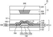
図1は、本実施形態に係る液晶表示装置の画素の構成を示す縦断面模式図である。図1において、液晶表示装置10は、TFTが形成されたTFTアレイ基板11、TFTアレイ基板11と対向して配置された対向基板としてのカラーフィルタ(CF)基板13、及び、両基板の間に挟持された液晶層12を備える。
FIG. 1 is a schematic vertical cross-sectional view showing a configuration of a pixel of the liquid crystal display device according to the present embodiment. In FIG. 1, a liquid
図2は、本実施形態に係る液晶表示装置におけるTFTアレイ基板11の構成を示す平面模式図である。図2において、ガラス基板101の主面上には、走査配線102及び信号配線106が格子状に配置されている。走査配線102及び信号配線106で区画された複数の画素領域には、走査配線102と信号配線106との交点近傍にスイッチング素子としてのTFT15が形成されている。FIG. 2 is a schematic plan view showing the configuration of the
TFT15が形成された領域をより詳細に見ると、図1に示すように、走査配線102が形成されたガラス基板101の主面上は、絶縁層としてのゲート絶縁膜103にて覆われている。ゲート絶縁膜103上には、走査配線102と重畳するようにIGZO半導体層104が形成されている。IGZO半導体層104上には、信号配線106及びドレイン電極107が形成されている。TFT15は、保護層108及び基板面を平坦化するための層間絶縁膜109によって覆われており、層間絶縁膜109の上には、画素電極110が形成されている。When the region where the
TFT15は、走査配線102の一部をゲート電極とし、ゲート絶縁膜103、チャネル層としてのIGZO半導体層104、信号配線106及びドレイン電極107によって構成される。The
走査配線102は、ここでは、走査配線層102a、102b及び102cが積層された構造を有する。走査配線102としては、例えば、走査配線層102a、102cがTiで形成され、走査配線層102bがAlで構成された積層構造であって、走査配線層102a、102cの膜厚が30〜150nmであり、走査配線層102bの膜厚が200〜500nmであるものが適用できる。Here, the
ゲート絶縁膜103としては、酸化シリコン(SiOx)、窒化シリコン(SiNx)等の無機材料が適用でき、ゲート絶縁膜103の膜厚は、例えば、200〜500nm程度とする。As the
IGZO半導体層104は、In、Ga、Zn、及び、Oを構成原子として含み、ストイキオメトリの状態を原子単位で100%としたときに、87〜95%の酸素含有量を有するIGZO半導体にて形成される。このような酸素含有量を有するIGZO半導体にてTFT15のチャネル層を形成することで、安定したトランジスタ特性を有するTFTアレイ基板11が得られる。IGZO半導体層104の膜厚は、特に限定されるものではなく、10〜300nm程度である。The
信号配線106は、その一部が、TFT15のソース電極として機能する。信号配線106としては、例えば、信号配線層106a、106bが積層された構造を有するものが挙げられる。ドレイン電極107は、ドレイン電極層107a、107bが積層された構造を有する。信号配線106及びドレイン電極107を形成する材料は、同一であっても異なっていてもよい。A part of the
信号配線106及びドレイン電極107としては、例えば、信号配線層106a及びドレイン電極層107aがTiにて形成され、信号配線層106b及びドレイン電極層107bがAlにて形成された、積層構造を有するものが挙げられる。信号配線層106a及びドレイン電極層107aの膜厚は、例えば、30〜150nm程度とし、信号配線層106b及びドレイン電極層107bの膜厚は、例えば、50〜400nm程度とする。The
上記保護層としては、例えば、SiOx、SiNx等の無機材料を、CVD法、スパッタ法等で成膜したものが適用でき、SiOx膜、SiNx膜だけでなくSiOx膜とSiNx膜との積層膜であってもよい。上記層間絶縁膜は、例えば、感光性樹脂を用いて形成される。As the protective layer, for example, an inorganic material such as SiOx, SiNx or the like formed by CVD, sputtering, or the like can be applied, and not only the SiOx film and SiNx film but also a laminated film of SiOx film and SiNx film. There may be. The interlayer insulating film is formed using, for example, a photosensitive resin.
画素電極110は、例えば、ITO等の透明電極材料にて形成し、その膜厚を50〜200nm程度とする。The
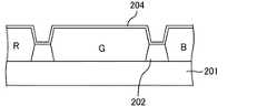
一方、CF基板13は、図1に示すように、ガラス基板201の主面上に、画素領域毎に赤(R)、青(B)、及び、緑(G)のCF層203を有する。各色のCF層203は、ブラックマトリクスと呼ばれる遮光部(図示せず)で仕切られている。基板の表面には、厚み50〜200nm程度の対向電極204が形成されており、遮光部が形成された領域には、フォトスペーサ(図示せず)が設けられている。On the other hand, as shown in FIG. 1, the
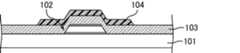
上記のような構成を有する液晶表示装置10の製造方法の一例について、具体例を挙げて、説明する。まず、TFTアレイ基板11の製造方法の一例について、図3〜図7を用いて説明する。図3〜図7は、本実施形態に係るTFTアレイ基板11を製造する各工程における断面模式図である。An example of a method for manufacturing the liquid
図3は、ガラス基板101の主面上に走査配線102が形成された状態を示す。走査配線102は、例えば、スパッタ法により、ガラス基板101の主面上に、膜厚30〜150nmのTi膜、膜厚200〜500nmのAl膜及び膜厚30〜150nmのTi膜をこの順番に成膜して走査配線層102a、102b及び102cを形成し、次いで、得られた積層膜をウェットエッチング処理及びレジスト剥離処理を含むフォトリソグラフィ法(以下、単にフォトリソグラフィ法と称す。)により所望の形状にパターン形成することにより得られる。FIG. 3 shows a state where the
図4は、図3に示す状態の基板の主面上をゲート絶縁膜103で覆い、更にIGZO半導体層104を形成した状態を示す。このような状態の基板は、絶縁膜形成工程を行い、次いで半導体層形成工程を行うことにより得られる。FIG. 4 shows a state where the main surface of the substrate in the state shown in FIG. 3 is covered with a
絶縁膜形成工程では、CVD法により、ガラス基板101及び走査配線102を覆うようにSiO2を厚み200〜500nmとなるように堆積してゲート絶縁膜103を形成する。半導体層形成工程では、基板面を法線方向から見たときに、走査配線102と重なる位置にIGZO半導体層104を形成する。In the insulating film forming step, a
IGZO半導体層104は、スパッタ法により、In−Ga−Zn−Oを含むターゲットを用いて、出力0.1〜2.0kWの条件で厚み10〜300nmとなるように堆積して、フォトリソグラフィ法によって所望の形状にパターン形成することにより得られる。ターゲットの組成比としては、例えば、In:Ga:Zn:O=1:1:1:4であるものや、In:Ga:Zn:O=2:2:1:7であるものが挙げられるが、本発明はこれに限定されるものではなく、成膜条件に応じてターゲットの組成を適宜設定すればよい。The
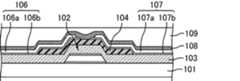
図5は、配線及び電極形成工程後の基板の状態を示す。配線及び電極形成工程では、図4に示す状態の基板に、更に信号配線106及びドレイン電極107を形成する。まず、スパッタ法を用いて、Tiを厚み30〜150nmとなるように堆積して、信号配線層106a及びドレイン電極層107aを形成する。次いで、Alを50〜400nmとなるように堆積して、信号配線層106b及びドレイン電極層107bを形成する。得られたTiとAlとの積層膜を、フォトリソグラフィ法を用いてパターニングすることにより、信号配線106及びドレイン電極107が形成される。FIG. 5 shows the state of the substrate after the wiring and electrode formation process. In the wiring and electrode forming step, a
図6は、保護層形成工程及び層間絶縁膜形成工程が行われた後の基板の状態を示す。保護層形成工程では、CVD法により、SiO2を厚み100〜700nmとなるように堆積して信号配線106及びドレイン電極107を含めて覆う保護層108を形成する。FIG. 6 shows the state of the substrate after the protective layer forming step and the interlayer insulating film forming step. In the protective layer forming step, a
層間絶縁膜形成工程では、感光性樹脂を用いて保護層108を覆うように層間絶縁膜109を形成する。In the interlayer insulating film forming step, the
図7は、画素電極110が形成された後の状態を示す。このような状態の基板は、例えば、スパッタ法によりITOを厚み50〜200nmとなるように層間絶縁膜109上に堆積させて薄膜を形成し、この薄膜をフォトリソグラフィ法によって所望の形状にパターニングして画素電極110を形成することで得られる。FIG. 7 shows a state after the
ここで、本実施形態においては、図6における保護層形成工程と層間絶縁膜形成工程との間に、保護層108をベーク処理するベーク処理工程を更に含む。本発明の液晶表示装置10においてIGZO半導体層104は、保護層108によってカバレッジされており、その後、後述のように層間絶縁膜形成工程を経てCF基板13と貼り合されることで外部と完全に遮断される。このような状態において、IGZO半導体層104に酸素脱離が起こるのは、IGZO半導体層104とゲート絶縁膜103との間、及び/又は、IGZO半導体層104と保護層108との間であると考えられる。Here, the present embodiment further includes a baking process for baking the
そこで、本実施形態においては、保護層108を形成した後に、各製造工程における処理温度のうち、最も高い処理温度にてベーク処理を行う。上記各製造工程であれば、IGZO半導体層104の形成温度が室温程度〜150℃程度であるのに対し、ゲート絶縁膜103、保護層108、及び、後述する層間絶縁膜109の形成時には、約200〜220℃以上の温度がかかる。したがって、ベーク処理は、ゲート絶縁膜103、保護層108、及び、層間絶縁膜109の形成時よりも更に高い温度(220℃以上)で行って、IGZO半導体層104の酸素含有量を制御する。ベーク処理の方法は特に限定されるものではないが、例えば、クリーンオーブンを用いて、大気雰囲気中でベークするという簡易な処理が適用できる。Therefore, in the present embodiment, after the
これにより、保護層108を介してIGZO半導体層104に酸素を補填する、又は、ゲート絶縁膜103及び保護層108からIGZO半導体層104へ酸素が補填され、IGZO半導体層104の酸素濃度が安定するとともにIGZO半導体層104において酸素脱離が生じることがなくなり、所望の酸素含有量を有するIGZO半導体層104が実現できる。酸素含有量は、得ようとするトランジスタ特性によって異なるが、90%以上であるとストイキオメトリからのズレが小さくなって、安定したトランジスタ特性を得ることができる。Accordingly, oxygen is supplied to the
CF基板13の製造方法の一例を、図8〜図10を用いて説明する。図8〜図10は、実施形態1に係る液晶表示装置を構成するCF基板の製造工程を示す平面模式図である。まず、図8に示すように、ガラス基板201の主面上に、黒色顔料を含む感光性樹脂をフォトリソグラフィ法により所望の形状にパターニングして遮光部202を形成する。次いで、遮光部202によって区画された領域に、赤(R)、緑(G)、青(B)の顔料を含む感光性樹脂を塗布して、CF層203R、203G、203Bを形成する。An example of a method for manufacturing the
そして、図9に示すように、基板の表面に、ITO等の透明電極材料をスパッタ法により厚み50〜200nmとなるように堆積させて、フォトリソグラフィ法により所望のパターン形状を有する対向電極204を形成する。更に、図10に示すように、遮光部202が形成された領域にフォトスペーサ205を形成する。フォトスペーサ205は、感光性樹脂を用いてフォトリソグラフィ法により、所望の形状にパターニングすることにより得られる。Then, as shown in FIG. 9, a transparent electrode material such as ITO is deposited on the surface of the substrate so as to have a thickness of 50 to 200 nm by sputtering, and the
上記のように製造されたTFTアレイ基板11及びCF基板13の表面には、ポリイミド樹脂が印刷法により塗布され配向膜(図示せず)が形成される。得られた両基板は、シール材を介して貼り合わされ、滴下法、注入法等の方法により基板間に液晶が封入される。そして、貼り合せた両基板を、ダイシングにより分断して、駆動装置、筐体、光源等の各種部材が必要に応じて設けられることにより、本実施形態に係る液晶表示装置10が得られる。On the surfaces of the
本実施形態においては、上述のように、特定の原子組成を有するIGZO半導体を形成するとともに、保護層108を形成した後に、上記製造工程における処理温度のうち最も高い処理温度にてベーク処理を行っているため、IGZO半導体層104の酸素濃度が安定し、ベーク処理後にIGZO半導体層104に酸素脱離が生じることがなくなり、これにより、信頼性の高い液晶表示装置10が実現できる。
以下に、本実施形態に係る液晶表示装置10の具体例について説明する。In the present embodiment, as described above, an IGZO semiconductor having a specific atomic composition is formed, and after the
Below, the specific example of the liquid
実施例1
実施形態1に係る液晶表示装置10において、In:Ga:Zn:O=1:1:1:4の割合であるスパッタリングターゲットを用いて、膜厚が50nmであるIGZO半導体層を形成した。Example 1
In the liquid
また、IGZO半導体層104の酸素含有量を制御するために、保護層108を成膜した後に、大気中において350℃で1時間のベーク処理を行った。ここでは、クリーンオーブンを用いて、大気中で350℃の温度で1時間のベーク処理を行った。In addition, in order to control the oxygen content of the
そして、IGZO半導体層104の表面から深さ約20nmの位置における構成原子の組成について、AES(Auger Electron Spectroscopy)分析により測定した。AES分析は、AES分析装置(JEOL社製、型番JAMP−9500F)を用いて、電子線照射条件:5kV、5nA、試料:75deg傾斜、中和条件:Arイオン10eV、1μA、検出器エネルギー分解能:dE/E=0.35%、検出エネルギーステップ:1.0eVの測定条件で分析を行い、In、Ga、Zn、O、Siの各構成原子について検出ピークを求めた。Then, the composition of constituent atoms at a position about 20 nm deep from the surface of the
ここで、AES分析の詳細について説明する。AES分析は、試料測定箇所に電子ビームを照射し、表面から放出されるオージェ電子の運動エネルギーと検出強度からスペクトルを得るものである。スペクトルのピーク位置や形状は元素固有のものであるため、ピーク位置や形状から元素を特定し、スペクトルの強度(振幅)から材料中の元素濃度を算出することで元素分析を行う。更に、スペクトルのピーク位置や形状は、原子の結合状態についても固有のものであるため、各元素中の化学結合状態(酸化状態など)の分析も可能である。Here, details of the AES analysis will be described. In AES analysis, a sample measurement site is irradiated with an electron beam, and a spectrum is obtained from the kinetic energy and detected intensity of Auger electrons emitted from the surface. Since the peak position and shape of the spectrum are unique to the element, element analysis is performed by specifying the element from the peak position and shape and calculating the element concentration in the material from the intensity (amplitude) of the spectrum. Furthermore, since the peak position and shape of the spectrum are unique to the bonding state of atoms, it is possible to analyze the chemical bonding state (oxidation state, etc.) in each element.
オージェ電子は、検出される膨大な電子量の中のごく一部分であるために、低周波成分のバックグランド影響を顕著に受ける。本実施例では、より正確な酸素含有量を求めるために、上記したAES分析に加えて、ラザフォード後方散乱分析(RBS:Rutherford Backscattering Spectrometry)及び粒子励起X線分析(PIXE:Particle Induced X−ray Emission)を行い、得られた値を用いて感度係数を補正した。Since Auger electrons are a small part of the enormous amount of electrons detected, the Auger electrons are significantly affected by the background of low-frequency components. In this example, in order to obtain a more accurate oxygen content, in addition to the AES analysis described above, Rutherford Backscattering Spectrometry (RBS) and Particle Excited X-ray Emission (PIXE) are used. The sensitivity coefficient was corrected using the obtained value.
すなわち、一般的に行われるように、スペクトルを微分して低周波成分のバックグランドを除去した上で、各元素のピーク強度から各元素固有の感度係数(装置付属の純元素の値を使用。)を用いて組成比を算出した。この測定結果に基づき、酸素含有量を下記一般式により求めた。In other words, as is commonly done, the spectrum is differentiated to remove the background of low-frequency components, and then the sensitivity coefficient specific to each element (the value of the pure element attached to the device is used from the peak intensity of each element). ) Was used to calculate the composition ratio. Based on this measurement result, the oxygen content was determined by the following general formula.
なお、各元素のピーク強度や形状は、化学結合状態が大きく変わると変化するため、組成比を高い精度で求めるには感度係数も補正する必要がある。そこで組成比算出に際して、下記の感度係数の補正を行った。In addition, since the peak intensity and shape of each element change when the chemical bonding state changes greatly, it is necessary to correct the sensitivity coefficient in order to obtain the composition ratio with high accuracy. Therefore, the following sensitivity coefficient was corrected when calculating the composition ratio.
具体的には、Inの酸化状態、還元状態を確認する為に、次の手法でIn(puremetal)およびIn(In2O3)のそれぞれの状態の存在比を計算した。すなわち、AES分析で得られたInの微分スペクトルを、In(puremetal)およびIn(In2O3)標準測定ピークにて非負拘束最小二乗法でフィッティングして各成分として分離し、ともに上記感度係数(装置付属の純元素の値を使用。)を用いて成分比を計算した。Specifically, in order to confirm the oxidation state and reduction state of In, the abundance ratio of each state of In (puremetal) and In (In2 O3 ) was calculated by the following method. In other words, the differential spectrum of In obtained by AES analysis is separated as each component by fitting with In (puremetal) and In (In2 O3 ) standard measurement peaks by the non-negative constrained least square method, and both of the above sensitivity coefficients The component ratio was calculated using the value of the pure element attached to the apparatus.
酸素含有量は、以下の一般式にて求めた。
{In(atomic%)×3/2+Ga(atomic%)×3/2+Zn(atomic%)}/O(atomic%)
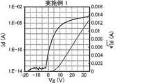
これにより、TFT15のチャネル層を構成するIGZO半導体の組成は、図11のグラフに示すようになった。なお、図11は、実施例1、並びに、後述する実施例2及び比較例1に係るTFTのチャネル層を構成する酸化物半導体の組成及び酸素含有量を示すグラフである。The oxygen content was determined by the following general formula.
{In (atomic%) x 3/2 + Ga (atomic%) x 3/2 + Zn (atomic%)} / O (atomic%)
As a result, the composition of the IGZO semiconductor constituting the channel layer of the
また、得られたTFTアレイ基板11のTFT特性を測定した。TFT特性は、図12に示すグラフの測定結果を基に、閾値(Vth)、移動度(μ)、サブスレッショルド・スイング値(S)の算出を行い、下記の判定基準に基づき判定した。各判定基準は、Vth、μ、及び、Sの全てを満たす必要があり、一つでも条件を満たしていない項目があれば、不適となる。
○:0V<Vth<10V、μ>5、S<1.5
△:−5<Vth<10V、μ≧1、S≦2.5
×:−10<Vth<15V、μ<1、S>2.5、又は、測定不能(−)
なお、図12は、実施例1に係る表示装置のTFTの電気特性を示すグラフである。図12に示すグラフにおいて、太線は、Vg−Id特性を、細線はVg−√Id特性をそれぞれ示す。なお、Vgはゲート電圧であり、Idはドレイン電流である。Further, the TFT characteristics of the obtained
○: 0V <Vth <10V, μ> 5, S <1.5
Δ: −5 <Vth <10V, μ ≧ 1, S ≦ 2.5
×: −10 <Vth <15V, μ <1, S> 2.5, or measurement impossible (−)
FIG. 12 is a graph showing the electrical characteristics of the TFT of the display device according to Example 1. In the graph shown in FIG. 12, the thick line indicates the Vg-Id characteristic, and the thin line indicates the Vg-√Id characteristic. Vg is a gate voltage, and Id is a drain current.
得られた測定結果を図12のグラフ及び下記表1に示す。The obtained measurement results are shown in the graph of FIG.

実施例2
IGZO半導体の組成を図11のグラフに示すようにした。また、ベーク処理は、実施例1と同様にクリーンオーブンを用いて、220℃で1時間の処理とした。そしてそれ以外は上記実施例1と同様にして各種物性値の測定を行った。
得られた測定結果を表1及び図13に示す。図13は、実施例2に係る表示装置のTFTの電気特性を示すグラフである。Example 2
The composition of the IGZO semiconductor was as shown in the graph of FIG. Further, the baking treatment was performed at 220 ° C. for 1 hour using a clean oven in the same manner as in Example 1. Other than that, various physical property values were measured in the same manner as in Example 1 above.
The obtained measurement results are shown in Table 1 and FIG. FIG. 13 is a graph showing the electrical characteristics of the TFT of the display device according to Example 2.
比較例1
IGZO半導体の組成を図11のグラフに示すようにした。また、保護層108の形成後に、ベーク処理を行わなかった。そしてそれ以外は上記実施例1と同様にして各種物性値の測定を行った。得られた測定結果を表1及び図14に示す。図14は、比較例1に係る表示装置のTFTの電気特性を示すグラフである。Comparative Example 1
The composition of the IGZO semiconductor was as shown in the graph of FIG. Further, no baking treatment was performed after the formation of the
表1及び図12〜図14に示すグラフから、実施例1及び2に係るTFTは、優れた電気特性を有することが分かる。また、比較例1に係るTFTは、薄膜トランジスタ特性に劣ることが明らかとなった。It can be seen from the graphs shown in Table 1 and FIGS. 12 to 14 that the TFTs according to Examples 1 and 2 have excellent electrical characteristics. Moreover, it became clear that the TFT according to Comparative Example 1 is inferior in thin film transistor characteristics.
なお、上記実施形態では、遮光部202及びCF層を対向基板の側に設けた例を挙げて説明したが、本発明はこれに限定されるものではなく、これらの部材はTFTアレイ基板11の側に形成することもできる。In the above embodiment, the example in which the
また、上記実施形態では、IGZO半導体をTFTのチャネル層として用いた例を挙げて説明したが、本発明はこれに限定されるものではなく、IGZO半導体は、透明電極等にも適用できる。Moreover, although the said embodiment gave and demonstrated the example which used the IGZO semiconductor as the channel layer of TFT, this invention is not limited to this, An IGZO semiconductor is applicable also to a transparent electrode etc.
更に、上記各実施形態では、液晶表示装置を例に挙げて説明したが、本発明はこれに限定されるものではなく、有機EL表示装置、プラズマディスプレイ表示装置、電界放出ディスプレイ表示装置等にも適用できる。Further, in each of the above embodiments, the liquid crystal display device has been described as an example, but the present invention is not limited to this, and the present invention is also applicable to an organic EL display device, a plasma display display device, a field emission display device, and the like. Applicable.
上述した実施例における各形態は、本発明の要旨を逸脱しない範囲において適宜組み合わされてもよい。Each form in the embodiments described above may be appropriately combined within a range not departing from the gist of the present invention.
なお、本願は、2009年6月29日に出願された日本国特許出願2009−154104号を基礎として、パリ条約ないし移行する国における法規に基づく優先権を主張するものである。該出願の内容は、その全体が本願中に参照として組み込まれている。In addition, this application claims the priority based on the laws and regulations in the Paris Convention or the country to which the transition is based on Japanese Patent Application No. 2009-154104 filed on June 29, 2009. The contents of the application are hereby incorporated by reference in their entirety.
10 液晶表示装置
11 TFTアレイ基板
12 液晶層
13 CF基板
15 TFT
101、201 ガラス基板
102a、102b、102c 走査配線層
102 走査配線
103 ゲート絶縁膜
104 酸化物半導体層
106a、106b 信号配線層
106 信号配線
107a、107b ドレイン電極層
107 ドレイン電極
108 保護層
109 層間絶縁膜
110 画素電極
121 チャネル保護層
202 遮光部
203R、203G、203B CF
204 対向電極
205 フォトスペーサ10 Liquid
101, 201
204
Claims (6)
Translated fromJapanese該酸化物半導体は、インジウム、ガリウム、亜鉛、及び、酸素を構成原子として含み、
該酸化物半導体の酸素含有量は、ストイキオメトリの状態を原子単位で100%としたときに、87〜95%であることを特徴とする酸化物半導体。An oxide semiconductor for a thin film transistor,
The oxide semiconductor contains indium, gallium, zinc, and oxygen as constituent atoms,
The oxygen content of the oxide semiconductor is 87 to 95% when the stoichiometry state is 100% in atomic units.
該薄膜トランジスタは、請求項1記載の酸化物半導体で形成されたチャネル層を有することを特徴とする薄膜トランジスタアレイ基板。A thin film transistor array substrate having thin film transistors on a main surface of the substrate,
2. A thin film transistor array substrate comprising a channel layer formed of the oxide semiconductor according to claim 1.
該保護層は、酸素原子を含む材料にて形成されていることを特徴とする請求項2記載の薄膜トランジスタアレイ基板。The thin film transistor further includes a protective layer covering the channel layer,
3. The thin film transistor array substrate according to claim 2, wherein the protective layer is made of a material containing oxygen atoms.
該製造方法は、
基板の主面上に形成された走査配線を絶縁膜で覆う絶縁膜形成工程と、
基板面を法線方向から見たときに、該走査配線と重なる位置に酸化物半導体層を形成する半導体層形成工程と、
該酸化物半導体層上に信号配線及びドレイン電極を形成する配線及び電極形成工程と、
該信号配線及び該ドレイン電極を覆う保護層を形成する保護層形成工程と、
該保護層を覆う層間絶縁膜を形成する層間絶縁膜形成工程とを含み、
該保護層形成工程と該層間絶縁膜形成工程との間に、ベーク処理工程を更に含むことを特徴とする薄膜トランジスタアレイ基板の製造方法。A method of manufacturing a thin film transistor array substrate having thin film transistors on a main surface of a substrate,
The manufacturing method is as follows:
An insulating film forming step of covering the scanning wiring formed on the main surface of the substrate with an insulating film;
A semiconductor layer forming step of forming an oxide semiconductor layer at a position overlapping with the scanning wiring when the substrate surface is viewed from the normal direction;
A wiring and electrode forming step of forming a signal wiring and a drain electrode on the oxide semiconductor layer;
A protective layer forming step of forming a protective layer covering the signal wiring and the drain electrode;
An interlayer insulating film forming step of forming an interlayer insulating film covering the protective layer,
A method of manufacturing a thin film transistor array substrate, further comprising a baking process between the protective layer forming step and the interlayer insulating film forming step.
Applications Claiming Priority (3)
| Application Number | Priority Date | Filing Date | Title |
|---|---|---|---|
| JP2009154104 | 2009-06-29 | ||
| JP2009154104 | 2009-06-29 | ||
| PCT/JP2010/053987WO2011001715A1 (en) | 2009-06-29 | 2010-03-10 | Oxide semiconductor, thin-film transistor array substrate and manufacturing method therefor, and display device |
Publications (1)
| Publication Number | Publication Date |
|---|---|
| JPWO2011001715A1true JPWO2011001715A1 (en) | 2012-12-13 |
Family
ID=43410799
Family Applications (1)
| Application Number | Title | Priority Date | Filing Date |
|---|---|---|---|
| JP2011520808APendingJPWO2011001715A1 (en) | 2009-06-29 | 2010-03-10 | Oxide semiconductor, thin film transistor array substrate, manufacturing method thereof, and display device |
Country Status (4)
| Country | Link |
|---|---|
| US (2) | US8865516B2 (en) |
| JP (1) | JPWO2011001715A1 (en) |
| CN (1) | CN102473727B (en) |
| WO (1) | WO2011001715A1 (en) |
Families Citing this family (16)
| Publication number | Priority date | Publication date | Assignee | Title |
|---|---|---|---|---|
| KR101812683B1 (en)* | 2009-10-21 | 2017-12-27 | 가부시키가이샤 한도오따이 에네루기 켄큐쇼 | Method for manufacturing semiconductor device |
| CN102906881B (en)* | 2010-05-21 | 2016-02-10 | 株式会社半导体能源研究所 | Semiconductor device |
| US20120032172A1 (en)* | 2010-08-06 | 2012-02-09 | Semiconductor Energy Laboratory Co., Ltd. | Semiconductor device |
| US8633044B2 (en)* | 2011-02-01 | 2014-01-21 | Sharp Kabushiki Kaisha | Display device and method for fabricating same |
| US8679905B2 (en)* | 2011-06-08 | 2014-03-25 | Cbrite Inc. | Metal oxide TFT with improved source/drain contacts |
| JP6013685B2 (en) | 2011-07-22 | 2016-10-25 | 株式会社半導体エネルギー研究所 | Semiconductor device |
| JP4982619B1 (en) | 2011-07-29 | 2012-07-25 | 富士フイルム株式会社 | Manufacturing method of semiconductor element and manufacturing method of field effect transistor |
| US9177872B2 (en)* | 2011-09-16 | 2015-11-03 | Micron Technology, Inc. | Memory cells, semiconductor devices, systems including such cells, and methods of fabrication |
| JP2014032999A (en)* | 2012-08-01 | 2014-02-20 | Panasonic Liquid Crystal Display Co Ltd | Thin film transistor and manufacturing method thereof |
| TWI566413B (en) | 2013-09-09 | 2017-01-11 | 元太科技工業股份有限公司 | Thin film transistor |
| CN104934330A (en)* | 2015-05-08 | 2015-09-23 | 京东方科技集团股份有限公司 | Film transistor and preparation method thereof, array substrate and display panel |
| JP2017123427A (en)* | 2016-01-08 | 2017-07-13 | 株式会社ジャパンディスプレイ | Thin film transistor |
| US10344982B2 (en) | 2016-12-30 | 2019-07-09 | General Electric Company | Compact multi-residence time bundled tube fuel nozzle having transition portions of different lengths |
| CN111900195B (en)* | 2020-09-08 | 2023-12-19 | 京东方科技集团股份有限公司 | Display substrate, preparation method and display device thereof |
| CN115735428A (en) | 2021-06-25 | 2023-03-03 | 京东方科技集团股份有限公司 | Oxide thin film transistor, manufacturing method thereof, and display device |
| CN115732571A (en)* | 2021-08-31 | 2023-03-03 | 福州京东方光电科技有限公司 | Metal oxide thin film transistor, manufacturing method thereof, and display panel |
Citations (4)
| Publication number | Priority date | Publication date | Assignee | Title |
|---|---|---|---|---|
| JP2006165531A (en)* | 2004-11-10 | 2006-06-22 | Canon Inc | Method for manufacturing field effect transistor |
| JP2008281988A (en)* | 2007-04-09 | 2008-11-20 | Canon Inc | Light emitting device and manufacturing method thereof |
| US20080299702A1 (en)* | 2007-05-28 | 2008-12-04 | Samsung Electronics Co., Ltd. | METHOD OF MANUFACTURING ZnO-BASED THIN FILM TRANSISTOR |
| JP2009099944A (en)* | 2007-09-28 | 2009-05-07 | Canon Inc | THIN FILM TRANSISTOR, MANUFACTURING METHOD THEREOF, AND DISPLAY DEVICE USING THE SAME |
Family Cites Families (25)
| Publication number | Priority date | Publication date | Assignee | Title |
|---|---|---|---|---|
| JP4170454B2 (en) | 1998-07-24 | 2008-10-22 | Hoya株式会社 | Article having transparent conductive oxide thin film and method for producing the same |
| WO2003040441A1 (en) | 2001-11-05 | 2003-05-15 | Japan Science And Technology Agency | Natural superlattice homologous single crystal thin film, method for preparation thereof, and device using said single crystal thin film |
| JP4164562B2 (en) | 2002-09-11 | 2008-10-15 | 独立行政法人科学技術振興機構 | Transparent thin film field effect transistor using homologous thin film as active layer |
| US7297977B2 (en) | 2004-03-12 | 2007-11-20 | Hewlett-Packard Development Company, L.P. | Semiconductor device |
| US7382421B2 (en) | 2004-10-12 | 2008-06-03 | Hewlett-Packard Development Company, L.P. | Thin film transistor with a passivation layer |
| AU2005302964B2 (en) | 2004-11-10 | 2010-11-04 | Canon Kabushiki Kaisha | Field effect transistor employing an amorphous oxide |
| US7829444B2 (en) | 2004-11-10 | 2010-11-09 | Canon Kabushiki Kaisha | Field effect transistor manufacturing method |
| US7791072B2 (en) | 2004-11-10 | 2010-09-07 | Canon Kabushiki Kaisha | Display |
| JP4560502B2 (en)* | 2005-09-06 | 2010-10-13 | キヤノン株式会社 | Field effect transistor |
| JP5006598B2 (en) | 2005-09-16 | 2012-08-22 | キヤノン株式会社 | Field effect transistor |
| JP5064747B2 (en) | 2005-09-29 | 2012-10-31 | 株式会社半導体エネルギー研究所 | Semiconductor device, electrophoretic display device, display module, electronic device, and method for manufacturing semiconductor device |
| EP1770788A3 (en) | 2005-09-29 | 2011-09-21 | Semiconductor Energy Laboratory Co., Ltd. | Semiconductor device having oxide semiconductor layer and manufacturing method thereof |
| JP5037808B2 (en)* | 2005-10-20 | 2012-10-03 | キヤノン株式会社 | Field effect transistor using amorphous oxide, and display device using the transistor |
| JP5000290B2 (en) | 2006-01-31 | 2012-08-15 | 出光興産株式会社 | TFT substrate and manufacturing method of TFT substrate |
| CN102244103A (en) | 2006-01-31 | 2011-11-16 | 出光兴产株式会社 | TFT substrate |
| JP2007293072A (en) | 2006-04-26 | 2007-11-08 | Epson Imaging Devices Corp | Electro-optical device manufacturing method, electro-optical device, and electronic apparatus |
| JP4609797B2 (en)* | 2006-08-09 | 2011-01-12 | Nec液晶テクノロジー株式会社 | Thin film device and manufacturing method thereof |
| JP2008140684A (en)* | 2006-12-04 | 2008-06-19 | Toppan Printing Co Ltd | Color EL display and manufacturing method thereof |
| KR101146574B1 (en)* | 2006-12-05 | 2012-05-16 | 캐논 가부시끼가이샤 | Method for manufacturing thin film transistor using oxide semiconductor and display apparatus |
| WO2008126879A1 (en)* | 2007-04-09 | 2008-10-23 | Canon Kabushiki Kaisha | Light-emitting apparatus and production method thereof |
| KR101325053B1 (en)* | 2007-04-18 | 2013-11-05 | 삼성디스플레이 주식회사 | Thin film transistor substrate and manufacturing method thereof |
| KR101334181B1 (en)* | 2007-04-20 | 2013-11-28 | 삼성전자주식회사 | Thin Film Transistor having selectively crystallized channel layer and method of manufacturing the same |
| KR101345376B1 (en)* | 2007-05-29 | 2013-12-24 | 삼성전자주식회사 | Fabrication method of ZnO family Thin film transistor |
| JP4623179B2 (en)* | 2008-09-18 | 2011-02-02 | ソニー株式会社 | Thin film transistor and manufacturing method thereof |
| KR101738996B1 (en)* | 2009-11-13 | 2017-05-23 | 가부시키가이샤 한도오따이 에네루기 켄큐쇼 | Device including nonvolatile memory element |
- 2010
- 2010-03-10JPJP2011520808Apatent/JPWO2011001715A1/enactivePending
- 2010-03-10WOPCT/JP2010/053987patent/WO2011001715A1/enactiveApplication Filing
- 2010-03-10CNCN201080029375.0Apatent/CN102473727B/enactiveActive
- 2010-03-10USUS13/377,824patent/US8865516B2/enactiveActive
- 2014
- 2014-09-05USUS14/478,055patent/US9076718B2/enactiveActive
Patent Citations (4)
| Publication number | Priority date | Publication date | Assignee | Title |
|---|---|---|---|---|
| JP2006165531A (en)* | 2004-11-10 | 2006-06-22 | Canon Inc | Method for manufacturing field effect transistor |
| JP2008281988A (en)* | 2007-04-09 | 2008-11-20 | Canon Inc | Light emitting device and manufacturing method thereof |
| US20080299702A1 (en)* | 2007-05-28 | 2008-12-04 | Samsung Electronics Co., Ltd. | METHOD OF MANUFACTURING ZnO-BASED THIN FILM TRANSISTOR |
| JP2009099944A (en)* | 2007-09-28 | 2009-05-07 | Canon Inc | THIN FILM TRANSISTOR, MANUFACTURING METHOD THEREOF, AND DISPLAY DEVICE USING THE SAME |
Also Published As
| Publication number | Publication date |
|---|---|
| US9076718B2 (en) | 2015-07-07 |
| CN102473727A (en) | 2012-05-23 |
| US20120091452A1 (en) | 2012-04-19 |
| CN102473727B (en) | 2015-04-01 |
| US20140367683A1 (en) | 2014-12-18 |
| WO2011001715A1 (en) | 2011-01-06 |
| US8865516B2 (en) | 2014-10-21 |
Similar Documents
| Publication | Publication Date | Title |
|---|---|---|
| JPWO2011001715A1 (en) | Oxide semiconductor, thin film transistor array substrate, manufacturing method thereof, and display device | |
| US10680117B2 (en) | Thin film transistor, method for manufacturing the same and display device comprising the same | |
| JP6599518B2 (en) | Thin film transistor including oxide semiconductor layer, method for manufacturing the same, and display device | |
| JP2013030682A (en) | Method of manufacturing field-effect transistor, field-effect transistor, display device, image sensor and x-ray sensor | |
| JP5795551B2 (en) | Method for manufacturing field effect transistor | |
| JP5995504B2 (en) | FIELD EFFECT TRANSISTOR AND METHOD FOR MANUFACTURING THE SAME, DISPLAY DEVICE, IMAGE SENSOR, AND X-RAY SENSOR | |
| JP6853421B2 (en) | Crystal oxide thin films, laminates and thin films | |
| US9773918B2 (en) | Metal oxide TFT with improved stability and mobility | |
| US20130099227A1 (en) | Oxide semiconductor, thin film transistor, and display device | |
| US8906739B2 (en) | Thin film transistor substrate and method for manufacturing same | |
| JP2015032655A (en) | Thin film transistor | |
| JP5869110B2 (en) | Thin film transistor, display device, image sensor and X-ray sensor | |
| JP6394518B2 (en) | Semiconductor device and manufacturing method thereof | |
| US20200357924A1 (en) | Oxide semiconductor thin film | |
| US8829513B2 (en) | Oxide semiconductor including Ga, In, Zn, and O and A thin film transistor and a display with the oxide semiconductor including Ga, In, Zn, and O | |
| US11024744B2 (en) | Semiconductor device and method for manufacturing the same | |
| US20130105788A1 (en) | Oxide semiconductor, thin film transistor, and display device |
Legal Events
| Date | Code | Title | Description |
|---|---|---|---|
| A131 | Notification of reasons for refusal | Free format text:JAPANESE INTERMEDIATE CODE: A131 Effective date:20130917 | |
| A131 | Notification of reasons for refusal | Free format text:JAPANESE INTERMEDIATE CODE: A131 Effective date:20140318 | |
| A521 | Request for written amendment filed | Free format text:JAPANESE INTERMEDIATE CODE: A523 Effective date:20140519 | |
| A02 | Decision of refusal | Free format text:JAPANESE INTERMEDIATE CODE: A02 Effective date:20141028 |