JPWO2010110252A1 - MOSFET and MOSFET manufacturing method - Google Patents
MOSFET and MOSFET manufacturing methodDownload PDFInfo
- Publication number
- JPWO2010110252A1 JPWO2010110252A1JP2011506053AJP2011506053AJPWO2010110252A1JP WO2010110252 A1JPWO2010110252 A1JP WO2010110252A1JP 2011506053 AJP2011506053 AJP 2011506053AJP 2011506053 AJP2011506053 AJP 2011506053AJP WO2010110252 A1JPWO2010110252 A1JP WO2010110252A1
- Authority
- JP
- Japan
- Prior art keywords
- mosfet
- semiconductor layer
- insulating film
- main surface
- plane
- Prior art date
- Legal status (The legal status is an assumption and is not a legal conclusion. Google has not performed a legal analysis and makes no representation as to the accuracy of the status listed.)
- Pending
Links
Images


Classifications
- H—ELECTRICITY
- H10—SEMICONDUCTOR DEVICES; ELECTRIC SOLID-STATE DEVICES NOT OTHERWISE PROVIDED FOR
- H10D—INORGANIC ELECTRIC SEMICONDUCTOR DEVICES
- H10D8/00—Diodes
- H10D8/01—Manufacture or treatment
- H10D8/051—Manufacture or treatment of Schottky diodes
- H—ELECTRICITY
- H10—SEMICONDUCTOR DEVICES; ELECTRIC SOLID-STATE DEVICES NOT OTHERWISE PROVIDED FOR
- H10D—INORGANIC ELECTRIC SEMICONDUCTOR DEVICES
- H10D1/00—Resistors, capacitors or inductors
- H10D1/60—Capacitors
- H10D1/62—Capacitors having potential barriers
- H10D1/66—Conductor-insulator-semiconductor capacitors, e.g. MOS capacitors
- H—ELECTRICITY
- H10—SEMICONDUCTOR DEVICES; ELECTRIC SOLID-STATE DEVICES NOT OTHERWISE PROVIDED FOR
- H10D—INORGANIC ELECTRIC SEMICONDUCTOR DEVICES
- H10D12/00—Bipolar devices controlled by the field effect, e.g. insulated-gate bipolar transistors [IGBT]
- H10D12/01—Manufacture or treatment
- H10D12/031—Manufacture or treatment of IGBTs
- H—ELECTRICITY
- H10—SEMICONDUCTOR DEVICES; ELECTRIC SOLID-STATE DEVICES NOT OTHERWISE PROVIDED FOR
- H10D—INORGANIC ELECTRIC SEMICONDUCTOR DEVICES
- H10D30/00—Field-effect transistors [FET]
- H—ELECTRICITY
- H10—SEMICONDUCTOR DEVICES; ELECTRIC SOLID-STATE DEVICES NOT OTHERWISE PROVIDED FOR
- H10D—INORGANIC ELECTRIC SEMICONDUCTOR DEVICES
- H10D30/00—Field-effect transistors [FET]
- H10D30/01—Manufacture or treatment
- H—ELECTRICITY
- H10—SEMICONDUCTOR DEVICES; ELECTRIC SOLID-STATE DEVICES NOT OTHERWISE PROVIDED FOR
- H10D—INORGANIC ELECTRIC SEMICONDUCTOR DEVICES
- H10D30/00—Field-effect transistors [FET]
- H10D30/60—Insulated-gate field-effect transistors [IGFET]
- H—ELECTRICITY
- H10—SEMICONDUCTOR DEVICES; ELECTRIC SOLID-STATE DEVICES NOT OTHERWISE PROVIDED FOR
- H10D—INORGANIC ELECTRIC SEMICONDUCTOR DEVICES
- H10D30/00—Field-effect transistors [FET]
- H10D30/60—Insulated-gate field-effect transistors [IGFET]
- H10D30/64—Double-diffused metal-oxide semiconductor [DMOS] FETs
- H10D30/66—Vertical DMOS [VDMOS] FETs
- H—ELECTRICITY
- H10—SEMICONDUCTOR DEVICES; ELECTRIC SOLID-STATE DEVICES NOT OTHERWISE PROVIDED FOR
- H10D—INORGANIC ELECTRIC SEMICONDUCTOR DEVICES
- H10D62/00—Semiconductor bodies, or regions thereof, of devices having potential barriers
- H10D62/10—Shapes, relative sizes or dispositions of the regions of the semiconductor bodies; Shapes of the semiconductor bodies
- H10D62/13—Semiconductor regions connected to electrodes carrying current to be rectified, amplified or switched, e.g. source or drain regions
- H10D62/149—Source or drain regions of field-effect devices
- H10D62/151—Source or drain regions of field-effect devices of IGFETs
- H10D62/156—Drain regions of DMOS transistors
- H10D62/157—Impurity concentrations or distributions
- H—ELECTRICITY
- H10—SEMICONDUCTOR DEVICES; ELECTRIC SOLID-STATE DEVICES NOT OTHERWISE PROVIDED FOR
- H10D—INORGANIC ELECTRIC SEMICONDUCTOR DEVICES
- H10D62/00—Semiconductor bodies, or regions thereof, of devices having potential barriers
- H10D62/10—Shapes, relative sizes or dispositions of the regions of the semiconductor bodies; Shapes of the semiconductor bodies
- H10D62/17—Semiconductor regions connected to electrodes not carrying current to be rectified, amplified or switched, e.g. channel regions
- H10D62/393—Body regions of DMOS transistors or IGBTs
- H—ELECTRICITY
- H10—SEMICONDUCTOR DEVICES; ELECTRIC SOLID-STATE DEVICES NOT OTHERWISE PROVIDED FOR
- H10D—INORGANIC ELECTRIC SEMICONDUCTOR DEVICES
- H10D62/00—Semiconductor bodies, or regions thereof, of devices having potential barriers
- H10D62/40—Crystalline structures
- H10D62/405—Orientations of crystalline planes
- H—ELECTRICITY
- H10—SEMICONDUCTOR DEVICES; ELECTRIC SOLID-STATE DEVICES NOT OTHERWISE PROVIDED FOR
- H10D—INORGANIC ELECTRIC SEMICONDUCTOR DEVICES
- H10D62/00—Semiconductor bodies, or regions thereof, of devices having potential barriers
- H10D62/80—Semiconductor bodies, or regions thereof, of devices having potential barriers characterised by the materials
- H10D62/83—Semiconductor bodies, or regions thereof, of devices having potential barriers characterised by the materials being Group IV materials, e.g. B-doped Si or undoped Ge
- H10D62/832—Semiconductor bodies, or regions thereof, of devices having potential barriers characterised by the materials being Group IV materials, e.g. B-doped Si or undoped Ge being Group IV materials comprising two or more elements, e.g. SiGe
- H10D62/8325—Silicon carbide
Landscapes
- Insulated Gate Type Field-Effect Transistor (AREA)
- Formation Of Insulating Films (AREA)
Abstract
Translated fromJapaneseDescription
Translated fromJapanese本発明は、MOSFETおよびMOSFETの製造方法に関する。 The present invention relates to a MOSFET and a method for manufacturing the MOSFET.
従来より、炭化ケイ素(SiC)を用いた半導体装置が知られている(たとえば、国際公開WO01/018872号パンフレット(以下、特許文献1と呼ぶ))。特許文献1では、面方位がほぼ{03−38}であり4H(Hexagonal)型ポリタイプのSiC基板を用いてMOS型電界効果トランジスタ(MOSFET:Metal−Oxide−Semiconductor Field−effect Transistor)を形成していることが記載されている。また当該MOSFETでは、ゲート酸化膜をドライ酸化(熱酸化)により形成していることが記載されている。上記特許文献1では、このようなMOSFETにおいて大きなチャネル移動度(約100cm2/Vs)を実現できることが記載されている。Conventionally, a semiconductor device using silicon carbide (SiC) is known (for example, International Publication WO01 / 018872 pamphlet (hereinafter referred to as Patent Document 1)). In
しかしながら、本発明者が検討した結果、上述したMOSFETにおいてチャネル移動度が十分に大きくならない場合があることを見い出した。チャネル移動度が大きくならない場合には、SiCを用いた半導体装置の優れた特性を安定して発揮させることができない。 However, as a result of studies by the present inventors, it has been found that the channel mobility may not be sufficiently increased in the MOSFET described above. If the channel mobility does not increase, the excellent characteristics of the semiconductor device using SiC cannot be stably exhibited.
この発明は、上記のような課題を解決するために成されたものであり、この発明の目的は、チャネル移動度を向上したMOSFETおよびMOSFETの製造方法を提供することである。 The present invention has been made to solve the above-described problems, and an object of the present invention is to provide a MOSFET and a method for manufacturing the MOSFET with improved channel mobility.
本発明者は、上述のようにMOSFETにおいて大きなチャネル移動度を再現性よく実現するために、チャネル移動度が小さくなる原因について鋭意研究した結果、本発明を完成した。つまり、チャネル移動度が小さくなるのは、ゲート酸化膜と当該ゲート酸化膜下に位置するSiC半導体膜との界面に存在するトラップ(以下、界面準位または、界面準位密度とも言う)に起因することを見い出した。これは、上述したMOSFETのしきい値電圧が理論値に比べて大幅に高くなっていることからも推定される。そこで、本発明者は、このような界面準位の影響を低減したMOSFETを実現するように鋭意研究した結果、本発明を見い出した。 The inventor has completed the present invention as a result of diligent research on the cause of the decrease in channel mobility in order to achieve high channel mobility with high reproducibility in the MOSFET as described above. That is, the channel mobility is reduced due to traps (hereinafter also referred to as interface state density or interface state density) present at the interface between the gate oxide film and the SiC semiconductor film located under the gate oxide film. I found something to do. This is also estimated from the fact that the threshold voltage of the MOSFET described above is significantly higher than the theoretical value. Therefore, the present inventor has found the present invention as a result of diligent research to realize a MOSFET in which the influence of the interface state is reduced.
すなわち、本発明のMOSFETは、{0001}面に対しオフ角が50°以上65°以下である主面を有する炭化ケイ素(SiC)基板と、SiC基板の主面上に形成された半導体層と、半導体層の表面に接触するように形成された絶縁膜とを備え、サブスレッショルドスロープが0.4V/Decade以下である。 That is, the MOSFET of the present invention includes a silicon carbide (SiC) substrate having a main surface with an off angle of 50 ° or more and 65 ° or less with respect to the {0001} plane, and a semiconductor layer formed on the main surface of the SiC substrate; And an insulating film formed so as to be in contact with the surface of the semiconductor layer, and a subthreshold slope is 0.4 V / Decade or less.
本発明のMOSFETの製造方法は、{0001}面に対しオフ角が50°以上65°以下である主面を有する炭化ケイ素(SiC)基板を準備する工程と、SiC基板の主面上に半導体層を形成する工程と、半導体層の表面に接触するように絶縁膜を形成する工程とを備え、サブスレッショルドスロープが0.4V/Decade以下である。 The method for manufacturing a MOSFET according to the present invention includes a step of preparing a silicon carbide (SiC) substrate having a main surface with an off angle of 50 ° to 65 ° with respect to the {0001} plane, and a semiconductor on the main surface of the SiC substrate. A step of forming a layer and a step of forming an insulating film so as to be in contact with the surface of the semiconductor layer, and a subthreshold slope is 0.4 V / Decade or less.
本発明者は、界面準位と関係を有するサブスレッショルドスロープに着目し、移動度が向上するサブスレッショルドスロープの範囲を鋭意研究した。その結果、サブスレッショルドスロープを0.4V/Decade以下にすることにより、絶縁膜と半導体層との界面近傍における界面準位密度を再現性よく低減できることを見い出した。これにより、半導体層において絶縁膜と対向する領域において、反転チャネル層となるキャリアの多くが界面準位にトラップされることを抑制することができる。したがって、チャネル移動度を向上することができる。 The inventor paid attention to the subthreshold slope having a relationship with the interface state, and intensively studied the range of the subthreshold slope where the mobility is improved. As a result, it was found that the interface state density in the vicinity of the interface between the insulating film and the semiconductor layer can be reduced with good reproducibility by setting the subthreshold slope to 0.4 V / Decade or less. Thereby, in the region facing the insulating film in the semiconductor layer, it is possible to suppress trapping of many carriers serving as the inversion channel layer at the interface state. Therefore, channel mobility can be improved.
なお、オフ角の下限を50°としたのは、オフ角が43.3°の(01−14)面からオフ角が51.5°の(01−13)面にかけてオフ角の増大とともにキャリア移動度の顕著な増大が見られたこと、また、上記(01−14)面から(01−13)面の間のオフ角の範囲には自然面が無いこと、といった理由による。 The lower limit of the off angle is set to 50 ° because the off angle increases from the (01-14) surface having an off angle of 43.3 ° to the (01-13) surface having an off angle of 51.5 ° as the carrier is increased. This is because a significant increase in mobility was observed, and there was no natural surface in the range of the off angle between the (01-14) surface and the (01-13) surface.
また、オフ角の上限を65°としたのは、オフ角が62.1°の(01−12)面からオフ角が90°の(01−10)面にかけてオフ角の増大とともにキャリア移動度の顕著な減少が見られたこと、また、上記(01−12)面から(01−10)面の間のオフ角の範囲には自然面が無いこと、といった理由による。 Further, the upper limit of the off angle is set to 65 ° because the off-angle increases and the carrier mobility increases from the (01-12) surface having an off angle of 62.1 ° to the (01-10) surface having an off angle of 90 °. For the reason that there is no natural surface in the range of the off angle between the (01-12) surface and the (01-10) surface.
上記MOSFETにおいて好ましくは、半導体層と、絶縁膜との間に、窒素原子を含む領域をさらに備えている。 Preferably, the MOSFET further includes a region containing nitrogen atoms between the semiconductor layer and the insulating film.
上記MOSFETにおいて好ましくは、半導体層と、絶縁膜との界面から10nm以内の領域における窒素濃度の最大値が1×1021cm-3以上である。Preferably, in the MOSFET, the maximum value of the nitrogen concentration in a region within 10 nm from the interface between the semiconductor layer and the insulating film is 1 × 1021 cm−3 or more.
上記MOSFETの製造方法において好ましくは、絶縁膜を形成する工程は、絶縁膜をドライ酸化により形成する工程と、絶縁膜を窒素原子を含有するガスを雰囲気ガスとして用いて熱処理する工程とを含む。 Preferably, in the MOSFET manufacturing method, the step of forming the insulating film includes a step of forming the insulating film by dry oxidation and a step of heat-treating the insulating film using a gas containing nitrogen atoms as an atmospheric gas.
本発明者は、半導体層と絶縁膜との界面近傍の窒素原子濃度を高めることにより、界面準位の影響を低減することを見い出した。このため、チャネル移動度をさらに向上したMOSFETを実現することができる。 The present inventor has found that the influence of the interface state is reduced by increasing the nitrogen atom concentration in the vicinity of the interface between the semiconductor layer and the insulating film. For this reason, a MOSFET with further improved channel mobility can be realized.
上記MOSFETにおいて好ましくは、半導体層はSiCよりなる。SiCは、バンドギャップが大きく、また最大絶縁破壊電界および熱伝導率はシリコン(Si)と比較して大きい一方、キャリアの移動度はシリコンと同程度に大きく、電子の飽和ドリフト速度および耐圧も大きい。このため、高効率化、高電圧化、および大容量化のMOSFETを実現できる。 In the MOSFET, the semiconductor layer is preferably made of SiC. SiC has a large band gap, and a maximum dielectric breakdown electric field and thermal conductivity are larger than those of silicon (Si), while carrier mobility is as large as that of silicon, and an electron saturation drift velocity and breakdown voltage are also large. . For this reason, MOSFET with high efficiency, high voltage, and large capacity can be realized.
上記MOSFETにおいては、上記SiC基板の主面のオフ方位が<11−20>方向±5°以下の範囲であってもよい。 In the MOSFET, the off orientation of the main surface of the SiC substrate may be in the range of <11-20> direction ± 5 ° or less.
<11−20>方向は、SiC基板における代表的なオフ方位である。そして、基板の製造工程におけるスライス加工のばらつき等に起因したオフ方位のばらつきを±5°とすることにより、SiC基板上へのエピタキシャル層の形成などを容易とし、MOSFETの製造を容易に実施することができる。 The <11-20> direction is a typical off orientation in the SiC substrate. Then, by setting the variation in off orientation caused by slicing variations in the substrate manufacturing process to ± 5 °, it is easy to form an epitaxial layer on the SiC substrate, and the MOSFET is easily manufactured. be able to.
上記MOSFETにおいては、上記SiC基板の主面のオフ方位が<01−10>方向±5°以下の範囲であってもよい。 In the MOSFET, the off orientation of the main surface of the SiC substrate may be in the range of <01-10> direction ± 5 ° or less.
<01−10>方向は、上記<11−20>方向と同様に、SiC基板における代表的なオフ方位である。そして、基板の製造工程におけるスライス加工のばらつき等に起因したオフ方位のばらつきを±5°とすることにより、SiC基板上へのエピタキシャル層の形成などを容易とし、MOSFETの製造を容易に実施することができる。 The <01-10> direction is a typical off orientation in the SiC substrate, similarly to the <11-20> direction. Then, by setting the variation in off orientation caused by slicing variations in the substrate manufacturing process to ± 5 °, it is easy to form an epitaxial layer on the SiC substrate, and the MOSFET is easily manufactured. be able to.
上記MOSFETにおいては、上記SiC基板の主面の面方位は、面方位{03−38}に対してオフ角が−3°以上+5°以下とすることができる。 In the MOSFET, the surface orientation of the main surface of the SiC substrate can be set to an off angle of −3 ° to + 5 ° with respect to the surface orientation {03-38}.
これにより、チャネル移動度をより一層向上させることができる。ここで、面方位{03−38}に対するオフ角を−3°以上+5°以下としたのは、チャネル移動度と当該オフ角との関係を調査した結果、この範囲内で特に高いチャネル移動度が得られたことに基づいている。 Thereby, channel mobility can be further improved. Here, the reason why the off angle with respect to the plane orientation {03-38} is set to −3 ° to + 5 ° is that, as a result of investigating the relationship between the channel mobility and the off angle, the channel mobility is particularly high within this range. Is based on the obtained.
ここで、「面方位{03−38}に対してオフ角が−3°以上+5°以下である」状態とは、<0001>方向およびオフ方位の基準としての<01−10>方向の張る平面への上記主面の法線の正射影と、{03−38}面の法線とのなす角度が−3°以上+5°以下である状態を意味し、その符号は、上記正射影が<01−10>方向に対して平行に近づく場合が正であり、上記正射影が<0001>方向に対して平行に近づく場合が負である。 Here, the state that “the off angle is −3 ° or more and + 5 ° or less with respect to the plane orientation {03-38}” means that the <0001> direction and the <01-10> direction as a reference for the off orientation are stretched. It means a state in which the angle between the normal projection of the principal surface to the plane and the normal of the {03-38} surface is -3 ° or more and + 5 ° or less, and the sign is The case where it approaches parallel to the <01-10> direction is positive, and the case where the orthographic projection approaches parallel to the <0001> direction is negative.
なお、上記主面の面方位は、実質的に{03−38}であることがより好ましく、上記主面の面方位は{03−38}であることがさらに好ましい。ここで、主面の面方位が実質的に{03−38}であるとは、基板の加工精度などを考慮して実質的に面方位が{03−38}とみなせるオフ角の範囲に基板の主面の面方位が含まれていることを意味し、この場合のオフ角の範囲としてはたとえば{03−38}に対してオフ角が±2°の範囲である。これにより、上述したチャネル移動度をより一層向上させることができる。 In addition, it is more preferable that the surface orientation of the main surface is substantially {03-38}, and it is further preferable that the surface orientation of the main surface is {03-38}. Here, the surface orientation of the main surface is substantially {03-38}, taking into account the processing accuracy of the substrate, etc., the substrate is within the range of the off angle where the surface orientation can be substantially regarded as {03-38}. In this case, the off angle range is, for example, a range of ± 2 ° with respect to {03-38}. As a result, the above-described channel mobility can be further improved.
上記MOSFETにおいては、基板の上記主面は、<01−10>方向における(0−33−8)面に対するオフ角が−3°以上+5°以下であってもよい。 In the MOSFET, the main surface of the substrate may have an off angle of not less than −3 ° and not more than + 5 ° with respect to the (0-33-8) plane in the <01-10> direction.
{03−38}面の中でも特にC(カーボン)面側の面である(0−33−8)面に近い面上に半導体層および絶縁膜を形成する構造を採用することにより、キャリア移動度が大幅に向上する。 By adopting a structure in which a semiconductor layer and an insulating film are formed on a surface close to the (0-33-8) surface which is the surface on the C (carbon) surface side among the {03-38} surface, carrier mobility is achieved. Is greatly improved.
ここで、本願において、六方晶の単結晶炭化珪素の(0001)面はシリコン面、(000−1)面はカーボン面と定義される。また、「<01−10>方向における(0−33−8)面に対するオフ角」とは、<000−1>方向およびオフ方位の基準としての<01−10>方向の張る平面への上記主面の法線の正射影と、(0−33−8)面の法線とのなす角度であり、その符号は、上記正射影が<01−10>方向に対して平行に近づく場合が正であり、上記正射影が<000−1>方向に対して平行に近づく場合が負である。そして、上記<01−10>方向における(0−33−8)面に対するオフ角が−3°以上+5°以下である主面とは、当該主面が炭化珪素結晶において上記条件を満たすカーボン面側の面であることを意味する。なお、本願において(0−33−8)面は、結晶面を規定するための軸の設定により表現が異なる等価なカーボン面側の面を含むとともに、シリコン面側の面を含まない。 Here, in the present application, the (0001) plane of hexagonal single crystal silicon carbide is defined as the silicon plane, and the (000-1) plane is defined as the carbon plane. The “off angle with respect to the (0-33-8) plane in the <01-10> direction” refers to the above described plane extending in the <01-10> direction as a reference for the <000-1> direction and the off orientation. This is the angle formed between the normal projection of the normal of the principal surface and the normal of the (0-33-8) plane, and the sign may be parallel to the <01-10> direction. It is positive, and the case where the orthogonal projection approaches parallel to the <000-1> direction is negative. And the main surface whose off angle with respect to the (0-33-8) plane in the <01-10> direction is −3 ° or more and + 5 ° or less is a carbon surface that satisfies the above conditions in the silicon carbide crystal. It means the side surface. In the present application, the (0-33-8) plane includes an equivalent carbon plane side plane whose expression differs depending on the setting of an axis for defining a crystal plane, and does not include a silicon plane side plane.
以上より、本発明のMOSFETおよびその製造方法によれば、サブスレッショルドスロープを0.4V/Decade以下にすることにより、チャネル移動度を向上することができる。 As described above, according to the MOSFET and the manufacturing method thereof of the present invention, the channel mobility can be improved by setting the subthreshold slope to 0.4 V / Decade or less.
以下、図面に基づいて本発明の実施の形態を説明する。なお、以下の図面において同一または相当する部分には同一の参照番号を付しその説明は繰返さない。また、本明細書中においては、個別方位を[]、集合方位を<>、個別面を()、集合面を{}でそれぞれ示している。また、負の指数については、結晶学上、”−”(バー)を数字の上に付けることになっているが、本明細書中では、数字の前に負の符号を付けている。 Hereinafter, embodiments of the present invention will be described with reference to the drawings. In the following drawings, the same or corresponding parts are denoted by the same reference numerals, and description thereof will not be repeated. In the present specification, the individual orientation is indicated by [], the collective orientation is indicated by <>, the individual plane is indicated by (), and the collective plane is indicated by {}. As for the negative index, “−” (bar) is attached on the number in crystallography, but in this specification, a negative sign is attached before the number.
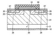
図1を参照して、本発明の一実施の形態におけるMOSFET1を説明する。本実施の形態におけるMOSFET1は、縦型のMOSFETである。 With reference to FIG. 1,
MOSFET1は、基板2と、半導体層21と、ウエル領域23と、ソース領域24と、コンタクト領域25と、絶縁膜26と、ゲート電極10と、ソース電極27と、層間絶縁膜28と、ドレイン電極12とを備えている。
基板2は、たとえばn+SiC基板である。基板2は、{0001}面に対しオフ角が50°以上65°以下、好ましくは{03−38}面である主面を有している。ここで、図2に示すように、{03−38}面とは、{0001}面に対して約55°(54.7°)の傾斜を有する面である。言い換えると、{03−38}面とは、<0001>軸方向に対して約35°(35.3°)の傾斜を有している面である。The
なお、基板2の主面のオフ方位は、<11−20>方向±5°以下の範囲であってもよく、<01−10>方向±5°以下の範囲であってもよい。また、基板2の主面の面方位は、面方位{03−38}に対してオフ角が−3°以上+5°以下であってもよい。また、基板2の主面は、<01−10>方向における(0−33−8)面に対するオフ角が−3°以上+5°以下であってもよい。これらの場合、チャネル移動度を向上することができる。特に、基板2の主面の面方位を(0−33−8)とすることにより、チャネル移動度を一層向上することができる。 The off orientation of the main surface of the
基板2の主面上に、たとえばn型SiCからなる半導体層21が形成されている。ウエル領域23は、半導体層21とpn接合をなすように、半導体層21の主面の一部に位置している。ウエル領域23は、たとえばp型SiCである。ソース領域24は、ウエル領域23とpn接合をなすように、ウエル領域23内の主面の一部に位置している。ソース領域24は、たとえばSiCである。コンタクト領域25は、ソース領域24とpn接合をなすように、ウエル領域23内の主面の一部に位置している。コンタクト領域25は、たとえばSiCである。 A
また半導体層21は、ソース領域24と同じ導電型(n)であり、ソース領域24よりも低い不純物濃度を有している。半導体層21は、たとえば10μmの厚みを有している。なお、半導体層21と、ソース領域24の不純物濃度との高低は特に限定されない。ソース領域24の不純物濃度は半導体層21の不純物濃度よりも高いことが好ましく、たとえば1×1018cm-3〜1×1020cm-3の不純物濃度を有する。n型不純物としては、たとえば窒素(N)、リン(P)などを用いることができる。The
またウエル領域23は、半導体層21と異なる第2の導電型(p)である。p型不純物としては、たとえばアルミニウム(Al)、ボロン(B)などを用いることができる。ウエル領域23は、たとえば5×1015cm-3〜5×1018cm-3の不純物濃度を有する。The
ウエル領域23におけるソース領域24と半導体層21とに挟まれた領域は、MOSFET1のチャネルとなる。本実施の形態では、nチャネルが形成されるように導電型を定めたが、pチャネルが形成されるように第1および第2の導電型を上述した内容と逆に定めてもよい。 A region sandwiched between the
絶縁膜26は、半導体層21とゲート電極10とを絶縁するためのものであり、ソース領域24と半導体層21とに挟まれる少なくともウエル領域23上に接触するように形成されている。 The insulating
ゲート電極10は、絶縁膜26上に形成され、ソース領域24と半導体層21とに挟まれるウエル領域23と少なくとも対向するように形成されている。なお、ゲート電極10は、ソース領域24と半導体層21との間に位置するウエル領域23上に対向するように形成されていれば、その他の領域上にさらに形成されていてもよい。 The
ソース領域24およびコンタクト領域25に電気的に接続するように、ソース領域24およびコンタクト領域25上にはソース電極27が形成されている。このソース電極27は、絶縁膜26によりゲート電極10と電気的に絶縁されている。また、基板2に電気的に接続するように、基板2において半導体層21と接触する面と反対側の面にはドレイン電極12が形成されている。 A
MOSFET1のサブスレッショルドスロープは、0.4V/Decade以下である。これにより、界面準位密度を低減することができるので、移動度を大きくすることができる。 The subthreshold slope of
ここで、上記サブスレッショルドスロープについて説明する。「サブスレッショルドスロープ(サブスレッショルドスイング、S値などとも言う)」とは、しきい値電圧以下において、ソース−ドレイン間に流れる電流を一桁増大させるのに必要なゲート電圧を意味する。サブスレッショルドスロープは、ゲート電圧をVGとし、ドレイン電流をIDとすると、下記の式1で表される。Here, the subthreshold slope will be described. “Sub-threshold slope (also referred to as sub-threshold swing, S value, etc.)” means a gate voltage required to increase the current flowing between the source and the drain by an order of magnitude below the threshold voltage. The subthreshold slope is expressed by the

また半導体層21と、絶縁膜26との界面には、窒素原子を含む領域が形成されていることが好ましい。たとえば、半導体層21と、絶縁膜26との界面から10nm以内の領域における窒素濃度の最大値が1×1021cm-3以上であることが好ましい。この場合、チャネル長を有するチャネル領域(半導体層21におけるウエル領域23の間の領域)での移動度(チャネル移動度)を十分大きな値とすることができる。In addition, a region containing nitrogen atoms is preferably formed at the interface between the
これは以下のような理由によると考えられる。すなわち、絶縁膜26と半導体層21との界面において、絶縁膜26を熱酸化などによって形成した場合に界面準位が多く形成される。そして、そのままではチャネル領域におけるチャネル移動度が極めて小さくなる。この問題に対し、上述のように当該絶縁膜26と半導体層21との界面領域に窒素原子を導入することにより、上述した界面準位の影響を低減してチャネル移動度を向上させることができる。 This is considered to be due to the following reasons. That is, many interface states are formed at the interface between the insulating
続いて、本実施の形態におけるMOSFET1の製造方法について説明する。
まず、図3に示すように、基板準備工程(S10)を実施する。この工程においては、面方位{0001}に対するオフ角が50°以上65°以下、たとえば面方位(03−38)または(0−33−8)である面を主面とする導電型がn型のSiC基板を基板2として準備する。このような基板は、たとえば(0001)面を主面とするインゴットから(03−38)面または(0−33−8)面が主面として露出するように基板2を切り出すといった手法により得ることができる。この工程では、製造するMOSFET1のチャネル移動度を一層向上させる観点から、(0−33−8)面が主面の基板2を準備することが特に好ましい。また、この基板2としては、たとえば基板の比抵抗が0.02Ωcmといった基板を用いてもよい。Then, the manufacturing method of MOSFET1 in this Embodiment is demonstrated.
First, as shown in FIG. 3, a substrate preparation step (S10) is performed. In this step, the conductivity type whose principal surface is a plane whose off-angle with respect to the plane orientation {0001} is 50 ° to 65 °, for example, the plane orientation (03-38) or (0-33-8) is n-type. The SiC substrate is prepared as the
次に、半導体層形成工程(S20)を実施する。具体的には、図4に示すように、基板2の主面上に半導体層21を形成する。半導体層21は、たとえば導電型がn型のSiCからなり、その厚みは10μmである。また、半導体層21におけるn型の不純物の濃度としては、1×1016cm-3という値を用いることができる。Next, a semiconductor layer forming step (S20) is performed. Specifically, as shown in FIG. 4, the
次に、注入工程(S30)を実施する。具体的には、フォトリソグラフィおよびエッチングを用いて形成した酸化膜をマスクとして用いて、導電型がp型の不純物(たとえばAl)を半導体層21に注入することにより、図5に示すようにウエル領域23を形成する。また、用いた酸化膜を除去した後、再度新たなパターンを有する酸化膜を、フォトリソグラフィおよびエッチングを用いて形成する。そして、当該酸化膜をマスクとして、n型の導電性不純物(たとえばP)を所定の領域に注入することにより、ソース領域24を形成する。また、同様の手法により、導電型がp型の導電性不純物を注入することにより、コンタクト領域25を形成する。その結果、図5に示すような構造を得る。 Next, an injection step (S30) is performed. Specifically, by using an oxide film formed by photolithography and etching as a mask, a p-type impurity (for example, Al) is implanted into the
このような注入工程(S30)の後、活性化アニール処理を行なう。この活性化アニール処理としては、たとえばアルゴン(Ar)ガスを雰囲気ガスとして用いて、加熱温度1700〜1800℃、加熱時間30分といった条件を用いることができる。活性化アニールにより、イオン注入領域の不純物を活性化するとともに、結晶性の回復を行なうことができる。 After such an implantation step (S30), an activation annealing process is performed. As this activation annealing treatment, for example, argon (Ar) gas is used as an atmospheric gas, and conditions such as a heating temperature of 1700 to 1800 ° C. and a heating time of 30 minutes can be used. By activation annealing, the impurities in the ion implantation region can be activated and the crystallinity can be recovered.
次に、ゲート絶縁膜形成工程(S40)を実施する。具体的には、図6に示すように、半導体層21、ウエル領域23、ソース領域24およびコンタクト領域25上を覆うように絶縁膜26を形成する。この絶縁膜26を形成するための条件としては、たとえばドライ酸化(熱酸化)を行なってもよい。このドライ酸化の条件としては、たとえば加熱温度を1200℃、加熱時間を30分といった条件を用いることができる。絶縁膜の厚みとしては、たとえば40nmという値を用いることができる。 Next, a gate insulating film formation step (S40) is performed. Specifically, as shown in FIG. 6, an insulating
次に、窒素アニール工程(S50)を実施する。具体的には、雰囲気ガスとしてたとえば一酸化窒素(NO)ガス、一酸化二窒素(N2O)ガスなどの窒素(N)原子を含有するガスを雰囲気ガスとして用いて熱処理する。雰囲気ガスは、窒素酸化物であることが好ましい。Next, a nitrogen annealing step (S50) is performed. Specifically, heat treatment is performed using a gas containing nitrogen (N) atoms such as nitrogen monoxide (NO) gas or dinitrogen monoxide (N2 O) gas as the atmosphere gas. The atmospheric gas is preferably nitrogen oxide.
熱処理の条件としては、たとえば加熱温度を1100℃以上1300℃以下、加熱時間を30分以上120分以下とする条件を用いることができる。この結果、絶縁膜26と下層の半導体層21、ウエル領域23、ソース領域24、コンタクト領域25との間の界面近傍に窒素原子を導入することができる。 As conditions for the heat treatment, for example, a heating temperature of 1100 ° C. to 1300 ° C. and a heating time of 30 minutes to 120 minutes can be used. As a result, nitrogen atoms can be introduced near the interface between the insulating
また、この窒素アニール工程の後、さらに、不活性ガスであるArガスを用いたアニールを行なってもよい。具体的には、Arガスを雰囲気ガスとして用いて、加熱温度を1100℃、加熱時間を60分といった条件を用いてもよい。 Further, after this nitrogen annealing step, annealing using Ar gas which is an inert gas may be further performed. Specifically, Ar gas may be used as the atmosphere gas, and the heating temperature may be 1100 ° C. and the heating time may be 60 minutes.
また、この窒素アニール工程の後、さらに、有機洗浄、酸洗浄、RCA洗浄などの表面洗浄化を行ってもよい。 Further, after this nitrogen annealing step, surface cleaning such as organic cleaning, acid cleaning, and RCA cleaning may be performed.
次に、電極形成工程(S60)を実施する。具体的には、絶縁膜26上に高濃度n型ポリSiなどのゲート電極10となるべき層をCVD(Chemical Vapor Deposition:化学蒸着)法などにより形成する。この層上に、フォトリソグラフィ法を用いて、ゲート電極10となるべき領域以外の領域が開口したパターンを有するレジスト膜を形成する。当該レジスト膜をマスクとして用いて、パターンから露出した層をRIE(Reactive Ion Etching:反応性イオンエッチング)などにより除去する。これにより、図7に示すように、ゲート電極10を形成できる。 Next, an electrode forming step (S60) is performed. Specifically, a layer to be the
次に、ゲート電極10を覆うように、SiO2などよりなる層間絶縁膜28となるべき絶縁膜をCVD法などにより形成する。たとえばCVD法、あるいはプラズマCVD法により酸化珪素(SiO2)、窒化珪素(Si3N4)を堆積しても良い。たとえばプラズマCVD法によるSiO2堆積の条件としては、テトラエトキシシラン(TEOS)と酸素(O2)との原料ガスを用いて、加熱温度350℃で、たとえば1μm堆積しても良い。この絶縁膜上に、フォトリソグラフィ法を用いて、層間絶縁膜28となるべき領域以外の領域が開口したパターンを有するレジスト膜を形成する。当該レジスト膜をマスクとして用いて、パターンから露出した絶縁膜をRIEなどにより除去する。これにより、図7に示すように、開口部を有する層間絶縁膜28を形成できる。Next, an insulating film to be the interlayer insulating
次に、層間絶縁膜28上に、フォトリソグラフィ法を用いて、ソース領域24の一部およびコンタクト領域25が開口したパターンを有するレジスト膜を形成する。パターンおよびレジスト上に、Niなどの導体膜を形成する。その後、レジストを除去(リフトオフ)することにより、絶縁膜26および層間絶縁膜28から開口したソース領域24およびコンタクト領域25と接触するソース電極27の一部を形成することができる。また、基板2の裏面上にドレイン電極12を形成する。ドレイン電極12は、たとえばニッケル(Ni)を用いることができる。ソース電極27およびドレイン電極12を形成した後に、たとえば合金化のための熱処理を行なう。これにより、図7に示すように、ソース電極27の一部およびドレイン電極12を形成することができる。 Next, a resist film having a pattern in which a part of the
次いで、先に形成した一部のソース電極27上に、上部ソース電極27を形成する。上部ソース電極27は、たとえばリフトオフ、エッチングなどを用いて形成することができる。 Next, the
以上説明したように、本実施の形態におけるMOSFET1は、{0001}面に対しオフ角が50°以上65°以下である主面、好ましくは{03−38}面を有するSiC基板2と、SiC基板2上に形成された半導体層21と、半導体層21の表面に接触するように形成された絶縁膜26とを備え、サブスレッショルドスロープが0.4V/Decade以下である。 As described above,
また本実施の形態におけるMOSFET1の製造方法は、{0001}面に対しオフ角が50°以上65°以下である主面、好ましくは{03−38}面を主面として有するSiC基板2を準備する基板準備工程(S10)と、SiC基板2上に半導体層21を形成する半導体層形成工程(S20)と、半導体層21の表面に接触するように絶縁膜26を形成するゲート絶縁膜形成工程(S40)とを備え、サブスレッショルドスロープが0.4V/Decade以下である。 In addition, the manufacturing method of
本発明者は、サブスレッショルドスロープを0.4V/Decade以下にすることにより、絶縁膜26と半導体層21との界面近傍における界面準位密度を効果的に低減できることを見い出した。これにより、半導体層21において絶縁膜26と対向する領域において、反転チャネル層となるキャリアの多くが界面準位にトラップされることを抑制することができる。さらに、トラップされたキャリアが固定電荷として振舞うことを抑制することができる。このため、ゲート電極の印加電圧(しきい値電圧)を小さく維持して、キャリアの多くがソース−ドレイン間の電流に寄与できる。したがって、チャネル移動度を向上することができるMOSFET1が得られる。このように、本実施の形態では、大きなチャネル移動度を再現性良く実現することができるので、MOSFET1の優れた特性を安定して発揮させることができる。 The inventor has found that the interface state density in the vicinity of the interface between the insulating
本実施例では、サブスレッショルドスロープを0.4V/Decade以下にすることによって、MOSFETの移動度を向上できる効果について調べた。 In this example, the effect of improving the mobility of the MOSFET was examined by setting the subthreshold slope to 0.4 V / Decade or less.
(本発明例1、2)
本発明例1、2のMOSFETは、基本的には図8に示す横型のMOSFET3を製造した。(Invention Examples 1 and 2)
As the MOSFETs of Examples 1 and 2 of the present invention, a lateral MOSFET 3 shown in FIG. 8 was basically manufactured.
具体的には、まず、基板準備工程(S10)では、基板2として(03−38)面を主面として有する4H−SiC基板を準備した。 Specifically, first, in the substrate preparation step (S10), a 4H—SiC substrate having a (03-38) plane as a main surface was prepared as the
次に、半導体層形成工程(S20)では、半導体層31として、0.8μm程度の厚みを有し、1×1016cm-3の不純物濃度を有するp型SiC層を形成した。このp型SiC層の主面は(03−38)面であった。Next, in the semiconductor layer forming step (S20), a p-type SiC layer having a thickness of about 0.8 μm and an impurity concentration of 1 × 1016 cm−3 was formed as the
次に、注入工程(S30)では、マスク材料としてSiO2を用いた。また、Pをn型不純物として1×1019cm-3の不純物濃度を有するソース領域24、ドレイン領域29を形成した。また、Alをp型不純物として1×1019cm-3の不純物濃度を有するコンタクト領域25を形成した。Next, in the implantation step (S30), SiO2 was used as a mask material. Further, a
注入工程(S30)の後、活性化アニール処理を行なった。この活性化アニール処理としては、Arガスを雰囲気ガスとして用いて、加熱温度1700〜1800℃、加熱時間30分と条件とした。 After the implantation step (S30), activation annealing treatment was performed. As this activation annealing treatment, Ar gas was used as the atmosphere gas, and the heating temperature was 1700 to 1800 ° C. and the heating time was 30 minutes.
次に、ゲート絶縁膜形成工程(S40)として、加熱温度を1200℃、加熱時間を本発明例1では30分、本発明例2では45分の条件でドライ酸化により、絶縁膜26としてゲート酸化膜を形成した。また、表面洗浄化を行った。 Next, as a gate insulating film forming step (S40), the gate oxide film is formed as the insulating
次に、窒素アニール工程(S50)として、NOを含む雰囲気中で、加熱温度を本発明例1では1100℃、本発明例2では1200℃で、加熱時間を120分とする条件で、熱処理を行なった。 Next, as a nitrogen annealing step (S50), heat treatment is performed in an atmosphere containing NO under the conditions that the heating temperature is 1100 ° C. in Invention Example 1, 1200 ° C. in Invention Example 2, and the heating time is 120 minutes. I did it.
次に、電極形成工程(S60)として、ポリSiよりなるゲート電極10、Niよりなるソース電極27、Niよりなるドレイン電極12を形成した。 Next, as an electrode formation step (S60), a
以上の工程(S10〜S60)を実施することにより、本発明例1、2のMOSFET3をそれぞれ製造した。 By performing the above steps (S10 to S60), MOSFETs 3 of Examples 1 and 2 of the present invention were manufactured.
(比較例1)
比較例1のMOSFETは、本発明例1のMOSFETの製造方法と基本的には同様の構成を備えていたが、基板の主面が(0001)面であった点、窒素アニール工程(S50)を実施しなかった点、ゲート絶縁膜形成工程(S40)において、加熱温度を1300℃、加熱時間を20分の条件とした点において異なっていた。(Comparative Example 1)
The MOSFET of Comparative Example 1 had basically the same configuration as the MOSFET manufacturing method of Inventive Example 1, but the main surface of the substrate was the (0001) plane, and the nitrogen annealing step (S50) In the gate insulating film forming step (S40), the heating temperature was 1300 ° C. and the heating time was 20 minutes.
(比較例2)
比較例2のMOSFETは、本発明例1のMOSFETの製造方法と基本的には同様の構成を備えていたが、基板の主面が(0001)面であった点、ゲート絶縁膜形成工程(S40)において加熱温度を1300℃、加熱時間を30分とした点、窒素アニール工程(S50)において加熱温度を1300℃、加熱時間を60分とした点において異なっていた。(Comparative Example 2)
The MOSFET of Comparative Example 2 had basically the same structure as the MOSFET manufacturing method of Inventive Example 1, but the main surface of the substrate was the (0001) plane, and the gate insulating film forming step ( The difference was that the heating temperature was 1300 ° C. and the heating time was 30 minutes in S40), and the heating temperature was 1300 ° C. and the heating time was 60 minutes in the nitrogen annealing step (S50).
(比較例3)
比較例3のMOSFETは、本発明例1のMOSFETの製造方法と基本的には同様の構成を備えていたが、基板の主面が(0001)面であった点、ゲート絶縁膜形成工程(S40)において加熱温度を1300℃、加熱時間を30分とした点、窒素アニール工程(S50)において加熱温度を1200℃、加熱時間を60分とした点において異なっていた。(Comparative Example 3)
The MOSFET of Comparative Example 3 had basically the same configuration as the MOSFET manufacturing method of Inventive Example 1, except that the main surface of the substrate was the (0001) plane, and the gate insulating film forming step ( The difference was that the heating temperature was 1300 ° C. and the heating time was 30 minutes in S40), and the heating temperature was 1200 ° C. and the heating time was 60 minutes in the nitrogen annealing step (S50).
(測定方法)
本発明例1、2および比較例1〜3のMOSFETについて、移動度およびサブスレッショルドスロープを測定した。(Measuring method)
For the MOSFETs of Invention Examples 1 and 2 and Comparative Examples 1 to 3, mobility and subthreshold slope were measured.
具体的には、移動度は、ソース−ドレイン間電圧VDS=0.1Vとし、ゲート電圧VGを印加して、ソース−ドレイン間電流IDSを測定した(ゲート電圧依存性を測定した)。そして、gm=(δIDS)/(δVG)として、チャネル移動度μ=gm×(L×d)/(W×ε×VDS)
(ここで、L:ゲート長、d:酸化膜厚、W:ゲート幅、ε:酸化膜の誘電率)
という式から、移動度のゲート電圧に対する最大値を求めた。Specifically, the mobility, the source - the drain voltage VDS = 0.1 V, by applying a gate voltage VG, the source - drain current between IDS was measured (the gate voltage dependence was measured) . Then, as gm = (δIDS ) / (δVG ), channel mobility μ = gm × (L × d) / (W × ε × VDS )
(Where L: gate length, d: oxide film thickness, W: gate width, ε: dielectric constant of oxide film)
From this equation, the maximum value of the mobility with respect to the gate voltage was obtained.
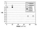
サブスレッショルドスロープは、ソース−ドレイン間電圧VDS=0.1Vとし、ゲート電圧VGを印加して、ゲート電圧VGがしきい値電圧以下の範囲において、ソース−ドレイン間電流IDSのゲート電圧に対する片対数プロットにおける直線領域で上記式1からサブスレッショルドスロープを測定した。その結果を図9に示す。The sub-threshold slope is the gate of the source-drain current IDS when the source-drain voltage VDS = 0.1 V, the gate voltage VG is applied, and the gate voltage VG is below the threshold voltage. The subthreshold slope was measured from the
図9に示すように、サブスレッショルドスロープが0.4の本発明例1および2のMOSFETは、74(cm2/Vs)以上92(cm2/Vs)以下の高い移動度を実現できた。一方、サブスレッショルドスロープが0.9〜1.0の比較例1〜3のMOSFETは、2.5(cm2/Vs)以上20(cm2/Vs)以下の低い移動度であった。As shown in FIG. 9, the MOSFETs of Examples 1 and 2 of the present invention examples 1 and 2 having a subthreshold slope of 0.4 could realize a high mobility of 74 (cm2 / Vs) or more and 92 (cm2 / Vs) or less. On the other hand, the MOSFETs of Comparative Examples 1 to 3 having a subthreshold slope of 0.9 to 1.0 had a low mobility of 2.5 (cm2 / Vs) to 20 (cm2 / Vs).
以上より、本実施例によれば、サブスレッショルドスロープを0.4V/Decade以下にすることにより、移動度を向上できることがわかった。 As described above, according to this example, it was found that the mobility can be improved by setting the subthreshold slope to 0.4 V / Decade or less.
ここで、本実施例では、基板2として(03−38)面を主面として有するSiC基板を用いたが、(0−33−8)面を主面として有するSiC基板を用いることにより、移動度をより向上できるという知見を本発明者は有している。 Here, in this example, an SiC substrate having the (03-38) plane as the main surface was used as the
本実施例では、サブスレッショルドスロープを0.4V/Decade以下にすることによって、界面準位密度を低減できる効果について調べた。 In this example, the effect of reducing the interface state density was examined by setting the subthreshold slope to 0.4 V / Decade or less.
一般的に、サブスレッショルドスロープ(S値)から界面準位密度を求めるためには、下記の式2において、既知の絶縁膜容量Cox、強反転時の空乏層容量Cd(たとえば強反転時の最大空乏層幅から計算できる)を用いて、界面準位密度Dit=0の場合の理論S値を求めることができる。In general, in order to obtain the interface state density from the subthreshold slope (S value), in the
なお、上記式2において、kはボルツマン定数を意味し、Tは絶対温度を意味し、Cdは強反転時の空乏層容量を意味し、Citは界面準位容量(Cit=qDit)を意味し、Coxは酸化膜容量を意味する。In the
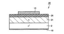
上記式2と実施例1でのS値とを比較することで、界面準位容量Citを算出し、界面準位密度Ditを導出することができる。しかし、上記式2から算出されるDit精度はあまり高くないことがわかった。このため、本実施例では、以下に示すように、図10に示すMOSキャパシタ30を作製し、その容量−電圧特性より、精度を向上して界面準位密度Ditを検討した。By comparing the
(本発明例3)
具体的には、まず、基板2として、本発明例1の基板準備工程(S10)と同様の基板を用いた。(Invention Example 3)
Specifically, first, as the
次に、基板2上に、本発明例1の半導体層形成工程(S20)と同様の半導体層21を形成した。 Next, the
次に、半導体層21上に、本発明例1のゲート絶縁膜形成工程(S40)と同様の絶縁膜26を形成した。 Next, an insulating
次に、加熱温度を1100℃、加熱時間を60分とした点を除き、本発明例1と同様の窒素アニール工程(S50)を実施した。 Next, a nitrogen annealing step (S50) similar to that of Inventive Example 1 was performed except that the heating temperature was 1100 ° C. and the heating time was 60 minutes.
次に、絶縁膜26上に、本発明例1の電極形成工程(S60)と同様のゲート電極10を形成した。また、裏面コンタクト電極18としてNiを形成した。 Next, on the insulating
以上より、本発明例3のMOSキャパシタを製造した。
(比較例4)
比較例4のMOSキャパシタは、本発明例3のMOSキャパシタの製造方法と基本的には同様の構成を備えていたが、ゲート絶縁膜形成工程(S40)において加熱温度を1200℃、加熱時間を30分とした点、窒素アニール工程(S50)を実施しなかった点において異なっていた。From the above, the MOS capacitor of Invention Example 3 was manufactured.
(Comparative Example 4)
The MOS capacitor of Comparative Example 4 had basically the same configuration as the manufacturing method of the MOS capacitor of Inventive Example 3, but the heating temperature was 1200 ° C. and the heating time was set in the gate insulating film forming step (S40). The difference was that the time was 30 minutes and the nitrogen annealing step (S50) was not performed.
(比較例5)
比較例5のMOSキャパシタは、本発明例3のMOSキャパシタの製造方法と基本的には同様の構成を備えていたが、基板の主面が(0001)面であった点、窒素アニール工程(S50)において加熱温度を1300℃、加熱時間を60分とした点において異なっていた。(Comparative Example 5)
The MOS capacitor of Comparative Example 5 had basically the same configuration as the manufacturing method of the MOS capacitor of Inventive Example 3, but the main surface of the substrate was the (0001) plane, and the nitrogen annealing step ( In S50), the heating temperature was 1300 ° C. and the heating time was 60 minutes.
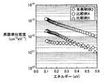
(測定方法)
本発明例3、比較例4および5のMOSキャパシタについて、エネルギーと、界面準位密度とを測定した。なお、エネルギーとは、MOS界面(半導体層21と絶縁膜26との界面)の半導体層側における導電帯の底を基準とした、バンドギャップ内のエネルギーとした。(Measuring method)
For the MOS capacitors of Invention Example 3 and Comparative Examples 4 and 5, energy and interface state density were measured. The energy is energy in the band gap with reference to the bottom of the conductive band on the semiconductor layer side of the MOS interface (interface between the
また界面準位密度は、容量C−電圧V特性よりHigh−Low法により測定した。その結果を図11に示す。 The interface state density was measured by the High-Low method from the capacitance C-voltage V characteristics. The result is shown in FIG.
図11に示すように、本発明例3のMOSキャパシタでは、MOS界面における界面準位が低かった。このことから、絶縁膜26を、窒素原子を含有するガスを雰囲気ガスとして用いて熱処理することにより、界面準位密度を低減できることがわかった。 As shown in FIG. 11, in the MOS capacitor of Invention Example 3, the interface state at the MOS interface was low. This indicates that the interface state density can be reduced by heat-treating the insulating
また、本発明例3のMOSキャパシタの条件でMOSFETを製造すると、サブスレッショルドスロープは0.4以下であった。このことから、サブスレッショルドスロープを0.4以下にすることにより、界面準位密度を低減できることがわかった。 Further, when the MOSFET was manufactured under the conditions of the MOS capacitor of Invention Example 3, the subthreshold slope was 0.4 or less. From this, it was found that the interface state density can be reduced by setting the subthreshold slope to 0.4 or less.
界面準位密度が低減されると、以下の効果を有していると考えられる。すなわち、ソース−ドレイン間の電流に寄与せずに界面準位にトラップされる反転電子を低減できる。このため、ソース−ドレイン間へ十分な電流を流すために必要な反転チャネル電子を形成するために必要なゲート電圧への印加、つまりしきい値電圧を小さくできる。以上より、サブスレッショルドスロープを0.4以下にすることにより、界面準位密度を低減できるので、移動度を向上できると考えられる。 When the interface state density is reduced, it is considered that the following effects are obtained. That is, inversion electrons trapped at the interface state without contributing to the source-drain current can be reduced. For this reason, the application to the gate voltage necessary for forming the inversion channel electrons necessary for flowing a sufficient current between the source and the drain, that is, the threshold voltage can be reduced. From the above, it is considered that the mobility can be improved because the interface state density can be reduced by setting the subthreshold slope to 0.4 or less.
一方、比較例4および5のMOSキャパシタでは、MOS界面における界面準位が高かった。比較例4、5のMOSキャパシタの条件でMOSFETを製造すると、サブスレッショルドスロープは0.4を超えていた。このことから、MOS界面に反転チャネルの電子がトラップされると、MOSFETの移動度が低下し、負の固定電荷として振舞うため、しきい値電圧が大きくなると考えられる。特許文献1では、比較例4のように窒素アニール工程(S50)を行なっていない。このため、上記特許文献1では、比較例4と同程度の界面準位密度となると考えられる。したがって、上記特許文献1のMOSFETでは、高い移動度を再現性よく実現することは困難であることが言える。 On the other hand, in the MOS capacitors of Comparative Examples 4 and 5, the interface state at the MOS interface was high. When a MOSFET was manufactured under the conditions of the MOS capacitors of Comparative Examples 4 and 5, the subthreshold slope exceeded 0.4. From this, it is considered that when the inversion channel electrons are trapped at the MOS interface, the mobility of the MOSFET is lowered and behaves as a negative fixed charge, so that the threshold voltage increases. In
以上より、本実施例によれば、サブスレッショルドスロープを0.4V/Decade以下にすることによって、移動度を向上できる根拠となる界面準位密度を低減できることがわかった。また、大きなチャネル移動度を再現性よく実現できると考えられる。 As described above, according to this example, it was found that the interface state density, which is the basis for improving the mobility, can be reduced by setting the subthreshold slope to 0.4 V / Decade or less. It is also considered that a large channel mobility can be realized with good reproducibility.
以上のように本発明の実施の形態および実施例について説明を行なったが、各実施の形態および実施例の特徴を適宜組み合わせることも当初から予定している。また、今回開示された実施の形態および実施例はすべての点で例示であって制限的なものではないと考えられるべきである。本発明の範囲は上記した説明ではなくて請求の範囲によって示され、請求の範囲と均等の意味および範囲内でのすべての変更が含まれることが意図される。 Although the embodiments and examples of the present invention have been described above, it is also planned from the beginning to appropriately combine the features of the embodiments and examples. The embodiments and examples disclosed this time should be considered as illustrative in all points and not restrictive. The scope of the present invention is defined by the terms of the claims, rather than the description above, and is intended to include any modifications within the scope and meaning equivalent to the terms of the claims.
本発明は、SiCからなる半導体層に絶縁膜が接触して形成されるMOSFETに有利に適用される。 The present invention is advantageously applied to a MOSFET formed by contacting an insulating film with a semiconductor layer made of SiC.
1,3 MOSFET、2 基板、10 ゲート電極、12 ドレイン電極、18 裏面コンタクト電極、21,31 半導体層、23 ウエル領域、24 ソース領域、25 コンタクト領域、26 絶縁膜、27 ソース電極、28 層間絶縁膜、29 ドレイン領域、30 MOSキャパシタ。 1, 3 MOSFET, 2 substrate, 10 gate electrode, 12 drain electrode, 18 back contact electrode, 21, 31 semiconductor layer, 23 well region, 24 source region, 25 contact region, 26 insulating film, 27 source electrode, 28 interlayer insulation Film, 29 drain region, 30 MOS capacitor.
Claims (10)
Translated fromJapanese前記炭化ケイ素基板(2)の前記主面上に形成された半導体層(21、31)と、
前記半導体層(21、31)の表面に接触するように形成された絶縁膜(26)とを備え、
サブスレッショルドスロープが0.4V/Decade以下である、MOSFET(1、3)。A silicon carbide substrate (2) having a main surface with an off-angle of 50 ° or more and 65 ° or less with respect to the {0001} plane;
A semiconductor layer (21, 31) formed on the main surface of the silicon carbide substrate (2);
An insulating film (26) formed so as to be in contact with the surface of the semiconductor layer (21, 31),
MOSFET (1, 3) with a subthreshold slope of 0.4 V / Decade or less.
前記炭化ケイ素基板(2)の前記主面上に半導体層(21、31)を形成する工程と、
前記半導体層(21、31)の表面に接触するように絶縁膜(26)を形成する工程とを備え、
サブスレッショルドスロープが0.4V/Decade以下である、MOSFET(1、3)の製造方法。Preparing a silicon carbide substrate (2) having a main surface with an off angle of 50 ° or more and 65 ° or less with respect to the {0001} plane;
Forming a semiconductor layer (21, 31) on the main surface of the silicon carbide substrate (2);
Forming an insulating film (26) in contact with the surface of the semiconductor layer (21, 31),
The manufacturing method of MOSFET (1, 3) whose subthreshold slope is 0.4 V / Decade or less.
Applications Claiming Priority (3)
| Application Number | Priority Date | Filing Date | Title |
|---|---|---|---|
| JP2009079408 | 2009-03-27 | ||
| JP2009079408 | 2009-03-27 | ||
| PCT/JP2010/054952WO2010110252A1 (en) | 2009-03-27 | 2010-03-23 | Mosfet and method for manufacturing mosfet |
Publications (1)
| Publication Number | Publication Date |
|---|---|
| JPWO2010110252A1true JPWO2010110252A1 (en) | 2012-09-27 |
Family
ID=42780945
Family Applications (1)
| Application Number | Title | Priority Date | Filing Date |
|---|---|---|---|
| JP2011506053APendingJPWO2010110252A1 (en) | 2009-03-27 | 2010-03-23 | MOSFET and MOSFET manufacturing method |
Country Status (8)
| Country | Link |
|---|---|
| US (1) | US8536583B2 (en) |
| EP (1) | EP2413364A4 (en) |
| JP (1) | JPWO2010110252A1 (en) |
| KR (1) | KR20110133541A (en) |
| CN (1) | CN102150271B (en) |
| CA (1) | CA2736950A1 (en) |
| TW (1) | TW201044587A (en) |
| WO (1) | WO2010110252A1 (en) |
Families Citing this family (6)
| Publication number | Priority date | Publication date | Assignee | Title |
|---|---|---|---|---|
| WO2012086257A1 (en)* | 2010-12-22 | 2012-06-28 | 住友電気工業株式会社 | Process for manufacture of silicon carbide semiconductor device |
| JP2012253293A (en)* | 2011-06-07 | 2012-12-20 | Sumitomo Electric Ind Ltd | Semiconductor device |
| JP6119100B2 (en)* | 2012-02-01 | 2017-04-26 | 住友電気工業株式会社 | Silicon carbide semiconductor device |
| JP6206012B2 (en)* | 2013-09-06 | 2017-10-04 | 住友電気工業株式会社 | Silicon carbide semiconductor device |
| JP7106881B2 (en)* | 2018-02-09 | 2022-07-27 | 株式会社デンソー | Silicon carbide substrate and silicon carbide semiconductor device |
| US11239079B2 (en) | 2020-03-19 | 2022-02-01 | Kabushiki Kaisha Toshiba | Semiconductor device, method for manufacturing semiconductor device, inverter circuit, drive device, vehicle, and elevator |
Citations (8)
| Publication number | Priority date | Publication date | Assignee | Title |
|---|---|---|---|---|
| JPH03145761A (en)* | 1989-11-01 | 1991-06-20 | Toshiba Corp | semiconductor equipment |
| JPH0799321A (en)* | 1993-05-27 | 1995-04-11 | Sony Corp | Method and apparatus for manufacturing thin film semiconductor element |
| JPH1027762A (en)* | 1996-03-18 | 1998-01-27 | Hyundai Electron Ind Co Ltd | Inductively coupled plasma CVD method and amorphous silicon thin film, silicon nitride film, and amorphous thin film transistor formed using the same |
| JP2002261275A (en)* | 2001-03-05 | 2002-09-13 | Shikusuon:Kk | MOS device |
| JP2005166930A (en)* | 2003-12-02 | 2005-06-23 | Matsushita Electric Ind Co Ltd | SiC-MISFET and method for manufacturing the same |
| JP2005183943A (en)* | 2003-11-25 | 2005-07-07 | Matsushita Electric Ind Co Ltd | Semiconductor element |
| JP3854508B2 (en)* | 1999-09-07 | 2006-12-06 | 株式会社シクスオン | SiC wafer, SiC semiconductor device, and method of manufacturing SiC wafer |
| JP4064436B2 (en)* | 2004-06-11 | 2008-03-19 | 松下電器産業株式会社 | Power element |
Family Cites Families (10)
| Publication number | Priority date | Publication date | Assignee | Title |
|---|---|---|---|---|
| US5587330A (en)* | 1994-10-20 | 1996-12-24 | Semiconductor Energy Laboratory Co., Ltd. | Method for manufacturing semiconductor device |
| JP4059939B2 (en)* | 1996-08-23 | 2008-03-12 | 株式会社半導体エネルギー研究所 | Power MOS device and manufacturing method thereof |
| JP3987796B2 (en) | 2000-10-03 | 2007-10-10 | クリー インコーポレイテッド | Method for producing oxide layer on silicon carbide layer using N2O |
| US7214984B2 (en) | 2003-11-25 | 2007-05-08 | Matsushita Electric Industrial Co., Ltd. | High-breakdown-voltage insulated gate semiconductor device |
| CN1938820A (en)* | 2004-03-26 | 2007-03-28 | 关西电力株式会社 | Bipolar semiconductor device and process for producing the same |
| JP4775102B2 (en)* | 2005-05-09 | 2011-09-21 | 住友電気工業株式会社 | Manufacturing method of semiconductor device |
| JP5037003B2 (en)* | 2005-11-25 | 2012-09-26 | 一般財団法人電力中央研究所 | Schottky barrier diode and method of using the same |
| US20080001173A1 (en) | 2006-06-23 | 2008-01-03 | International Business Machines Corporation | BURIED CHANNEL MOSFET USING III-V COMPOUND SEMICONDUCTORS AND HIGH k GATE DIELECTRICS |
| US20090032873A1 (en)* | 2007-07-30 | 2009-02-05 | Jeffrey Scott Cites | Ultra thin single crystalline semiconductor TFT and process for making same |
| JP5504597B2 (en)* | 2007-12-11 | 2014-05-28 | 住友電気工業株式会社 | Silicon carbide semiconductor device and manufacturing method thereof |
- 2010
- 2010-03-23TWTW099108547Apatent/TW201044587A/enunknown
- 2010-03-23CNCN201080002563.4Apatent/CN102150271B/ennot_activeExpired - Fee Related
- 2010-03-23KRKR1020117004212Apatent/KR20110133541A/ennot_activeWithdrawn
- 2010-03-23CACA2736950Apatent/CA2736950A1/ennot_activeAbandoned
- 2010-03-23JPJP2011506053Apatent/JPWO2010110252A1/enactivePending
- 2010-03-23EPEP10756048.4Apatent/EP2413364A4/ennot_activeWithdrawn
- 2010-03-23USUS13/063,298patent/US8536583B2/enactiveActive
- 2010-03-23WOPCT/JP2010/054952patent/WO2010110252A1/enactiveApplication Filing
Patent Citations (8)
| Publication number | Priority date | Publication date | Assignee | Title |
|---|---|---|---|---|
| JPH03145761A (en)* | 1989-11-01 | 1991-06-20 | Toshiba Corp | semiconductor equipment |
| JPH0799321A (en)* | 1993-05-27 | 1995-04-11 | Sony Corp | Method and apparatus for manufacturing thin film semiconductor element |
| JPH1027762A (en)* | 1996-03-18 | 1998-01-27 | Hyundai Electron Ind Co Ltd | Inductively coupled plasma CVD method and amorphous silicon thin film, silicon nitride film, and amorphous thin film transistor formed using the same |
| JP3854508B2 (en)* | 1999-09-07 | 2006-12-06 | 株式会社シクスオン | SiC wafer, SiC semiconductor device, and method of manufacturing SiC wafer |
| JP2002261275A (en)* | 2001-03-05 | 2002-09-13 | Shikusuon:Kk | MOS device |
| JP2005183943A (en)* | 2003-11-25 | 2005-07-07 | Matsushita Electric Ind Co Ltd | Semiconductor element |
| JP2005166930A (en)* | 2003-12-02 | 2005-06-23 | Matsushita Electric Ind Co Ltd | SiC-MISFET and method for manufacturing the same |
| JP4064436B2 (en)* | 2004-06-11 | 2008-03-19 | 松下電器産業株式会社 | Power element |
Also Published As
| Publication number | Publication date |
|---|---|
| US8536583B2 (en) | 2013-09-17 |
| TW201044587A (en) | 2010-12-16 |
| CN102150271B (en) | 2014-06-11 |
| CN102150271A (en) | 2011-08-10 |
| US20110169016A1 (en) | 2011-07-14 |
| EP2413364A1 (en) | 2012-02-01 |
| WO2010110252A1 (en) | 2010-09-30 |
| CA2736950A1 (en) | 2010-09-30 |
| KR20110133541A (en) | 2011-12-13 |
| EP2413364A4 (en) | 2013-05-08 |
Similar Documents
| Publication | Publication Date | Title |
|---|---|---|
| JPWO2010110253A1 (en) | MOSFET and MOSFET manufacturing method | |
| TWI440180B (en) | Silicon carbide semiconductor device and manufacturing method thereof | |
| JP5603008B2 (en) | Method for forming SiCMOSFET having large inversion layer mobility | |
| JP4843854B2 (en) | MOS device | |
| US8564017B2 (en) | Silicon carbide semiconductor device and method for manufacturing same | |
| WO2010116886A9 (en) | Insulated gate bipolar transistor | |
| JP2012209422A (en) | Igbt | |
| JPWO2010116887A1 (en) | Insulated gate field effect transistor | |
| US20110062450A1 (en) | Silicon carbide semiconductor device | |
| JPWO2010110252A1 (en) | MOSFET and MOSFET manufacturing method | |
| WO2015015926A1 (en) | Silicon-carbide semiconductor device and manufacturing method therefor | |
| JP2018206872A (en) | Semiconductor device | |
| JP2006156478A (en) | Silicon carbide semiconductor device and manufacturing method thereof | |
| JPWO2011089687A1 (en) | Silicon carbide semiconductor device and manufacturing method thereof | |
| JP4956904B2 (en) | Silicon carbide semiconductor device and manufacturing method thereof | |
| JP5564781B2 (en) | Silicon carbide semiconductor device and manufacturing method thereof | |
| JP3941641B2 (en) | Silicon carbide semiconductor device manufacturing method and silicon carbide semiconductor device manufactured by the manufacturing method | |
| JP5187118B2 (en) | Silicon carbide semiconductor device and method for manufacturing silicon carbide semiconductor device |
Legal Events
| Date | Code | Title | Description |
|---|---|---|---|
| A621 | Written request for application examination | Free format text:JAPANESE INTERMEDIATE CODE: A621 Effective date:20121026 | |
| A521 | Request for written amendment filed | Free format text:JAPANESE INTERMEDIATE CODE: A523 Effective date:20130730 | |
| A131 | Notification of reasons for refusal | Free format text:JAPANESE INTERMEDIATE CODE: A131 Effective date:20140311 | |
| A521 | Request for written amendment filed | Free format text:JAPANESE INTERMEDIATE CODE: A523 Effective date:20140424 | |
| A02 | Decision of refusal | Free format text:JAPANESE INTERMEDIATE CODE: A02 Effective date:20140805 |