JPWO2010073397A1 - Input/Output Unit - Google Patents
Input/Output UnitDownload PDFInfo
- Publication number
- JPWO2010073397A1 JPWO2010073397A1JP2010543729AJP2010543729AJPWO2010073397A1JP WO2010073397 A1JPWO2010073397 A1JP WO2010073397A1JP 2010543729 AJP2010543729 AJP 2010543729AJP 2010543729 AJP2010543729 AJP 2010543729AJP WO2010073397 A1JPWO2010073397 A1JP WO2010073397A1
- Authority
- JP
- Japan
- Prior art keywords
- input
- output
- back unit
- card
- connector
- Prior art date
- Legal status (The legal status is an assumption and is not a legal conclusion. Google has not performed a legal analysis and makes no representation as to the accuracy of the status listed.)
- Granted
Links
Images


Classifications
- H—ELECTRICITY
- H05—ELECTRIC TECHNIQUES NOT OTHERWISE PROVIDED FOR
- H05K—PRINTED CIRCUITS; CASINGS OR CONSTRUCTIONAL DETAILS OF ELECTRIC APPARATUS; MANUFACTURE OF ASSEMBLAGES OF ELECTRICAL COMPONENTS
- H05K7/00—Constructional details common to different types of electric apparatus
- H05K7/14—Mounting supporting structure in casing or on frame or rack
- H05K7/1461—Slidable card holders; Card stiffeners; Control or display means therefor
Landscapes
- Engineering & Computer Science (AREA)
- Microelectronics & Electronic Packaging (AREA)
- Mounting Of Printed Circuit Boards And The Like (AREA)
Abstract
Translated fromJapaneseDescription
Translated fromJapanese本発明は、工作機械の数値制御装置等の制御装置と、センサー、電動バルブ及びランプ等のフィールド機器とを接続し入出力信号の授受を行なう入出力ユニットに関するものである。The present invention relates to an input/output unit that connects a control device, such as a numerical control device for a machine tool, to field devices, such as sensors, electric valves, and lamps, and transmits and receives input/output signals.
従来、工業用制御機器と被制御対象となるフィールド機器との間の信号授受を仲介する入出力ユニットにおいて、前記工業用制御機器とバス接続される入出力ネストと、この入出力ネストに収容されると共に、この工業用制御機器で取り扱う信号形式とフィールド機器で取り扱う信号形式との変換を行う入出力カードと、この入出力ネストに機械的に装着され、フィールド機器と接続された信号線が結線されると共に、この信号線が入出力カードと電気的に接続されるインターフェイス部と、を具備する入出力ユニットがある(例えば、特許文献1参照)。Conventionally, in an input/output unit that mediates the transmission and reception of signals between an industrial control device and a controlled field device, there is an input/output unit that comprises an input/output nest that is bus-connected to the industrial control device, an input/output card that is housed in the input/output nest and converts between the signal format handled by the industrial control device and the signal format handled by the field device, and an interface section that is mechanically attached to the input/output nest and to which a signal line connected to the field device is connected and which electrically connects the signal line to the input/output card (see, for example, Patent Document 1).
この入出力ユニットでは、入出力カードと工業用制御機器のバックユニットとの間に中継基板(バックボード)を介在させており、この中継基板には、バックユニット上のコネクタと接続されるコネクタ(1つ)と、複数(4枚)の入出力カードと接続される複数(4つ)のコネクタが装着されている。In this input/output unit, a relay board (backboard) is interposed between the input/output card and the back unit of the industrial control equipment, and this relay board is equipped with one connector that connects to the connector on the back unit, and multiple (four) connectors that connect to multiple (four) input/output cards.
入出力サブユニットをバックユニットに接続するときは、中継基板を、樹脂成型品である入出力ネスト内に保持し、まず、入出力ネストをバックユニットにネジで取付ける。そのとき同時に、入出力ネスト内の中継基板のコネクタとバックユニット上のコネクタが嵌合する。When connecting the I/O subunit to the back unit, the relay board is held inside the I/O nest, which is a resin molded product, and the I/O nest is first attached to the back unit with screws. At the same time, the connector of the relay board inside the I/O nest fits into the connector on the back unit.
バックユニットに取付けられた入出力ネスト内には、入出力カードと接続される中継基板の複数のコネクタが配置されており、樹脂成型品で形成された入出力ネストのカード挿入スロットに沿って、入出力カードを一枚ずつ挿入してコネクタ接続を行なう。Inside the input/output nest attached to the back unit, multiple connectors of the relay board that are connected to the input/output cards are arranged, and the input/output cards are inserted one by one along the card insertion slots of the input/output nest, which is made from molded resin, to connect the connectors.
しかしながら、上記の従来の入出力サブユニットでは、入出力ネストをバックユニットに取付けた後、さらに、複数(4枚)の入出力カードを一枚ずつ挿入してコネクタ接続を行なう必要があり、組立て工数が多い、という問題がある。また、入出力カードとバックユニットとを接続するための中継基板(バックボード)を必要とし、電気的接続の信頼性が低い上に、コストアップとなる、という問題がある。However, with the above conventional I/O subunits, after the I/O nest is attached to the back unit, multiple (four) I/O cards must be inserted one by one to connect the connectors, which requires a large number of assembly steps. In addition, a relay board (backboard) is required to connect the I/O cards to the back unit, which reduces the reliability of the electrical connection and increases costs.
本発明は、上記に鑑みてなされたものであって、組立工数が少なく、電気的接続の信頼性が高く、低コストな入出力ユニットを得ることを目的とする。The present invention has been made in consideration of the above, and aims to obtain an input/output unit that requires fewer assembly steps, has highly reliable electrical connections, and is low cost.
上述した課題を解決し、目的を達成するために、本発明は、制御装置のバックユニットに並列に配置された複数のバックユニットコネクタに夫々嵌合される前側コネクタを備え、前記制御装置と複数のフィールド機器との間の信号授受を仲介する入出力ユニットにおいて、前記前側コネクタを基板の前縁に装着し、前記フィールド機器のコネクタと嵌合される複数の後側コネクタを前記基板の後縁に装着し、前記信号授受を仲介する電子回路を実装した入出力カードと、前側に前記バックユニットのガイド孔に挿入される複数のガイド軸を有し、前記入出力カードを保持するカードホルダーと、から成る複数の入出力サブユニットと、後面が開放された箱状に形成され、前記入出力サブユニットが内面との間に間隙を有して挿入される複数のスロットが形成され、前板に、前記バックユニットコネクタが内面との間に間隙を有して外側から挿入される長孔及び前記ガイド軸が内面との間に間隙を有して内側から挿通される軸孔が形成され、前記複数の入出力サブユニットを前記夫々のスロット内に保持した状態で前記バックユニットに取付けられるケースと、を備えることを特徴とする。In order to solve the above-mentioned problems and achieve the object, the present invention provides an input/output unit that has a front connector that is fitted to a plurality of back unit connectors arranged in parallel in a back unit of a control device and mediates the transmission and reception of signals between the control device and a plurality of field devices, the front connector being attached to the front edge of a board and a plurality of rear connectors that are fitted to the connectors of the field devices being attached to the rear edge of the board, the input/output subunits being composed of an input/output card having an electronic circuit that mediates the transmission and reception of signals, and a card holder having a plurality of guide shafts on the front side that are inserted into guide holes in the back unit and holding the input/output card, and a case that is formed in a box shape with an open rear face, has a plurality of slots into which the input/output subunits are inserted with a gap between them and the inner surface, and has a front plate formed with an elongated hole through which the back unit connector is inserted from the outside with a gap between it and the inner surface and an axial hole through which the guide shaft is inserted from the inside with a gap between it and the inner surface, and is attached to the back unit with the plurality of input/output subunits held in their respective slots.
本発明にかかる入出力ユニットは、組立工数が少なく、電気的接続の信頼性が高く、低コストである、という効果を奏する。The input/output unit of the present invention has the advantages of requiring fewer assembly steps, providing highly reliable electrical connections, and being low cost.
10 入出力カード
11 基板
11a 基準孔
11b 縦長基準孔
11c 締結孔
12 前側コネクタ
13 後側コネクタ
14 電子回路
20 カードホルダー
20a 後板
20b 長孔
20c 天板
20d 底板
20e スナップフィット
20f 把持部
20g 側板
20h 位置決めピン
20i 前板
20j 切欠き部
20k ガイド軸
20m 係止爪
20n 凸条(突起部)
20p 台座
20r ねじ孔
20s スナップフィット
30 入出力サブユニット
40 ケース
40a 天板
40b 底板
40c 溝
40d スロット
40e ガイド部
40f スナップフィット嵌合部
40g 係止孔
40h 支持溝
40i 前板
40j 長孔
40k 軸孔
40m、40n ねじ通し孔
40p 側板
40s 間隙
40t 間隙
41 ねじ
50 バックユニット
50a ガイド孔
50b ねじ孔
51 バックユニットコネクタ
91 入出力ユニット REFERENCE SIGNS LIST 10 I/
以下に、本発明にかかる入出力ユニットの実施の形態を図面に基づいて詳細に説明する。なお、この実施の形態によりこの発明が限定されるものではない。Below, an embodiment of the input/output unit according to the present invention is explained in detail with reference to the drawings. Note that the present invention is not limited to this embodiment.
実施の形態
図1は、本発明の入出力ユニットの実施の形態の入出力カードを示す斜視図である。図1に示すように、入出力カード10は、矩形の基板11と、基板11の表面の前縁に装着され、後述のバックユニットコネクタ51(図5参照)と嵌合される前側コネクタ12と、基板11の表面の後縁に装着され、図示しない各フィールド機器(センサー、電動バルブ及びランプ等)のコネクタと嵌合される複数の後側コネクタ13と、基板11に実装され前側コネクタ12と後側コネクタ13の間を電気的に接続し、図示しない制御装置で取扱う信号形式とフィールド機器で取扱う信号形式との変換を行う電子回路14と、を備えている。1 is a perspective view showing an input/output card according to an embodiment of the input/output unit of the present invention. As shown in Fig. 1, an input/
基板11の前縁下部には、入出力カード10を後述のカードホルダー20(図2参照)に位置決めする基準孔11aが設けられ、前縁上部には、縦長基準孔11bが設けられている。また、基板11の後部上下部には、締結孔11cが設けられている。The
図2は、実施の形態のカードホルダーを示す斜視図である。図2に示すように、カードホルダー20は、樹脂により、一側面が開放された薄型の直方体箱状に成型されている。後板20aには、入出力カード10の複数の後側コネクタ13が頭を出す長孔20bが形成されている。Figure 2 is a perspective view of a card holder according to an embodiment. As shown in Figure 2, the
天板20c及び底板20dの後部の外側には、略L字形のスナップフィット20eが設けられている。スナップフィット20eには、係止爪20mが設けられている。天板20c及び底板20dの後部の両側部には、突起としての凸条20n(図3参照)が設けられている。天板20c及び底板20dの後端部には、把持部20fが設けられている。A generally L-
側板20gの前縁上下部には、入出力カード10を設置する台座20pが形成され、台座20pには、基板11の基準孔11a及び縦長基準孔11bに嵌合し、入出力カード10をカードホルダー20上で位置決めする位置決めピン20hが設けられている。位置決めピン20hの前方の前板20iの後側には、位置決めピン20hに嵌合された入出力カード10の前縁に係合して入出力カード10を抜け止めするスナップフィット20sが設けられている。また、側板20gの後部上下部には、台座にねじ孔20rが設けられている。A
前板20iの上部及び下部を除く大部分は、入出力カード10の前側コネクタ12が頭を出す切欠き部20jが形成されている。前板20iの上部及び下部には、バックユニットコネクタ51(図5参照)の上下近傍のバックユニット50に設けられたガイド孔50aに挿入される2本の先細のガイド軸20kが設けられている。側板20g、天板20c及び底板20dには、多数の風孔が設けられている。Most of the
図3は、実施の形態の入出力サブユニットをケースに挿入する前の状態を示す斜視図である。図3に示すように、入出力サブユニット30は、一側面が開放された薄型の直方体箱状に形成されたカードホルダー20と、カードホルダー20の側板20g上に位置決め固定された入出力カード10と、を備えて成る。3 is a perspective view showing the state before inserting the input/output subunit of the embodiment into the case. As shown in Fig. 3, the input/
入出力カード10は、カードホルダー20の側板20gに形成された台座20pに設置され、位置決めピン20hに基板11の基準孔11a及び縦長基準孔11bを嵌合させ、スナップフィット20sに前縁を係止され、図示しないねじにより締結孔11cを通してねじ孔20rに締結されている。The input/
入出力カード10は、台座20p上に設置されることによって、カードホルダー20との垂直方向の位置決めがなされ、位置決めピン20hに基準孔11a及び縦長基準孔11bを嵌合させることによって前後方向及び上下方向の位置決めがなされる。縦長基準孔11bは、位置決めピン20h間のピッチと基準孔11a、11b間のピッチの製作誤差を吸収する。The input/
入出力カード10がカードホルダー20に位置決め固定された状態で、入出力カード10の複数の後側コネクタ13は、カードホルダー20の後板20aに形成された長孔20bから頭を出している。前側コネクタ12は、カードホルダー20の前板20iの切欠き部20jから頭を出している。When the I/
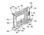
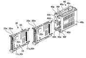
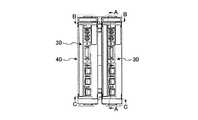
図4は、実施の形態の入出力サブユニットをケースに挿入した状態を示す前方斜視図であり、図5は、実施の形態の入出力ユニットをバックユニットに取付ける前の状態を示す斜視図であり、図6は、実施の形態の入出力ユニットを示す後面図であり、図7は、図6のA−A線に沿う断面図であり、図8は、図7のD部拡大図であり、図9は、図6のB−B線に沿う断面図であり、図10は、図9のE部拡大図であり、図11は、図6のC−C線に沿う断面図である。Figure 4 is a front oblique view showing the input/output subunit of the embodiment inserted into the case, Figure 5 is an oblique view showing the state before the input/output unit of the embodiment is attached to the back unit, Figure 6 is a rear view showing the input/output unit of the embodiment, Figure 7 is a cross-sectional view along line A-A in Figure 6, Figure 8 is an enlarged view of portion D in Figure 7, Figure 9 is a cross-sectional view along line B-B in Figure 6, Figure 10 is an enlarged view of portion E in Figure 9, and Figure 11 is a cross-sectional view along line C-C in Figure 6.
図3及び図4に示すように、ケース40は、樹脂により、後面が開放された直方体箱状に成型されている。天板40a及び底板40bの幅方向中央には、前後方向全長に亘るU字状の溝40cが形成されている。ケース40の内部空間は、溝40cにより、2つのスロット40dに分割されている。3 and 4, the
夫々のスロット40dの上下には、入出力サブユニット30の挿入をガイドするU字状のガイド部40eが形成されている。スロット40dの縦横内面寸法は、カードホルダー20の縦横外形寸法より略2mm大きく形成され、スロット40d(ガイド部40e)の内面とカードホルダー20との間には、全周に亘って略1mmの間隙40s(図8、図10参照)ができるようになっている。Above and below each
ガイド部40eの後端部には、カードホルダー20のスナップフィット20eを嵌合し入出力カード30の後部を弾力的に保持するスナップフィット嵌合部40fが形成されている。スナップフィット嵌合部40fには、スナップフィット20eに設けられた係止爪20mを係止して入出力サブユニット30をスロット40dから抜け止めする係止孔40gが設けられている。A snap-
図3及び図10に示すように、ガイド部40eの後部の両側部には、カードホルダー20の後部に設けられた突起としての複数の凸条20nを嵌合して入出力サブユニット30の後部を点支持する複数の支持溝40hが設けられている。As shown in Figures 3 and 10, a plurality of
図4に示すように、ケース40の前板40iには、2つのスロット40dの夫々に対応して、バックユニットコネクタ51(図5参照)を挿入可能な2つの長孔40jと、入出力サブユニット30のガイド軸20kが挿通される合計4つの軸孔40kが設けられている。軸孔40kは、長孔40jの上下近傍に設けられている。As shown in Fig. 4, the
長孔40jの縦横内面寸法は、バックユニットコネクタ51の外形寸法より縦横略2mm大きく形成され、長孔40jの内面と長孔40jに挿入されるユニットコネクタ51との間には、全周に亘って略1mmの間隙ができるようになっている。また、軸孔40kの内径寸法は、ガイド軸20kの外径寸法より略2mm大きく形成され、軸孔40kの内面とガイド軸との間には、全周に亘って略1mmの間隙40t(図8参照)ができるようになっている。The vertical and horizontal inner dimensions of the
また、溝40cの前方の前板40iには、ケース40をバックユニット50のねじ孔50bに締結するねじ41を挿通するねじ通し孔40m、40nが設けられている。ケース40の天板40a、底板40b及び側板40pには、多数の風穴が設けられている。In addition, the
図6〜図11に示すように、ケース40の2つのスロット40dの夫々に入出力サブユニット30を挿入し、カードホルダー20の前板20iをケース40の前板40iの内面に当接させると、入出力サブユニット30のガイド軸20kが、前板40iの軸孔40kに挿通される。このとき、スロット40d(ガイド部40e)の内面と入出力サブユニット30との間には、略1mmの間隙40s(図8、図10参照)があり、軸孔40kの内面とガイド軸20kとの間には、略1mmの間隙40t(図8参照)がある。6 to 11, when the input/
また、カードホルダー20の天板20c及び底板20dの後部外側に設けられたスナップフィット20eが、ケース40のスロット40d(ガイド部40e)の後端上下に形成されたスナップフィット嵌合部40fに嵌合して弾性的に支持され、スナップフィット20eに設けられた係止爪20mが、スナップフィット嵌合部40fに設けられた係止孔40gに係止され、入出力サブユニット30がケース40から抜け出るのを防止する。In addition, the snap fits 20e provided on the rear outer sides of the
さらに、カードホルダー20の天板20c及び底板20dの後部の両側部に設けられた突起部としての複数の凸条20nが、ガイド部40eの後部両側に設けられた複数の支持溝40hに嵌合し、入出力サブユニット30は、支持溝40hに凸条20nが点支持され、前部が、スロット40dと内面との間の略1mmの間隙内で左右上下に揺動可能である。Furthermore,
凸条20nと支持溝40hの内面との間の間隙は、略0.2mmに設定されている。それ故、凸条20nは、支持溝40hにより上下左右方向とも拘束され、点支持された状態となる。入出力ユニット91は、以上説明したケース40と、ケース40に挿入保持された入出力サブユニット30とを備えて成る。入出力サブユニット30は、後部に設けられた凸条20nが支持溝40hに点支持され、前部が左右上下に揺動するので、揺動角度は小さい。The gap between the
入出力ユニット91のガイド軸20kを、バックユニット50のガイド孔50aに挿入していくと、バックユニットコネクタ51が、入出力サブユニット30の前側コネクタ12に嵌合する。When the
このとき、バックユニット50に並列に配置された2つのバックユニットコネクタ51の配置位置が組立誤差によりずれていても、スロット40d内で、ガイド軸20k及び前側コネクタ12が、ずれたバックユニットコネクタ51に追従して小さな傾斜角度で揺動してずれ、バックユニットコネクタ51と前側コネクタ12とを無理なく嵌合することができる。At this time, even if the positions of the two rear unit connectors 51 arranged in parallel on the rear unit 50 are misaligned due to assembly errors, the
この状態で、ねじ41をケース40のねじ通し孔40m、40nを通してバックユニット50のねじ孔50bにねじ込み、入出力ユニット91を、バックユニット50に取付ける。In this state, screw 41 through the screw holes 40m, 40n of the
本発明の実施の形態では、1つのケース40に2つの入出力サブユニット30を挿入保持する例を説明したが、1つのケースに3つ以上の入出力サブユニット30を挿入保持するようにしてもよい。In the embodiment of the present invention, an example has been described in which two input/
以上説明したように、実施の形態の入出力ユニット91は、入出力カード10とバックユニット50とを接続するための中継基板を必要としないので、組立工数が少なく、電気的接続の信頼性が高く、低コストである。As described above, the input/output unit 91 of the embodiment does not require an intermediate board to connect the input/
以上のように、本発明にかかる入出力ユニットは、工作機械の数値制御装置等の入出力ユニットとして有用である。As described above, the input/output unit of the present invention is useful as an input/output unit for numerical control devices of machine tools, etc.
Claims (4)
Translated fromJapanese前記前側コネクタを基板の前縁に装着し、前記フィールド機器のコネクタと嵌合される複数の後側コネクタを前記基板の後縁に装着し、前記信号授受を仲介する電子回路を実装した入出力カードと、
前側に前記バックユニットのガイド孔に挿入される複数のガイド軸を有し、前記入出力カードを保持するカードホルダーと、
から成る複数の入出力サブユニットと、
後面が開放された箱状に形成され、前記入出力サブユニットが内面との間に間隙を有して挿入される複数のスロットが形成され、前板に、前記バックユニットコネクタが内面との間に間隙を有して外側から挿入される長孔及び前記ガイド軸が内面との間に間隙を有して内側から挿通される軸孔が形成され、前記複数の入出力サブユニットを前記夫々のスロット内に保持した状態で前記バックユニットに取付けられるケースと、
を備えることを特徴とする入出力ユニット。 An input/output unit includes a front connector that is fitted to a plurality of back unit connectors arranged in parallel in a back unit of a control device, and mediates signal transmission between the control device and a plurality of field devices,
an input/output card having the front connector attached to a front edge of a substrate, a plurality of rear connectors attached to a rear edge of the substrate to be mated with connectors of the field devices, and an electronic circuit for mediating the signal transmission and reception;
a card holder having a plurality of guide shafts on a front side thereof that are inserted into guide holes of the back unit and that holds the input/output card;
A plurality of input/output subunits each comprising:
a case formed in a box shape with an open rear face, with a plurality of slots formed therein into which the input/output subunits are inserted with a gap between the slots and the inner surface, and a front plate formed with an elongated hole into which the back unit connector is inserted from the outside with a gap between the slots and the inner surface, and an axial hole into which the guide shaft is inserted from the inside with a gap between the slots and the inner surface, and the case is attached to the back unit with the plurality of input/output subunits held in their respective slots;
An input/output unit comprising:
Applications Claiming Priority (1)
| Application Number | Priority Date | Filing Date | Title |
|---|---|---|---|
| PCT/JP2008/073823WO2010073397A1 (en) | 2008-12-26 | 2008-12-26 | Input/output unit |
Publications (2)
| Publication Number | Publication Date |
|---|---|
| JPWO2010073397A1true JPWO2010073397A1 (en) | 2012-05-31 |
| JP4959002B2 JP4959002B2 (en) | 2012-06-20 |
Family
ID=42287064
Family Applications (1)
| Application Number | Title | Priority Date | Filing Date |
|---|---|---|---|
| JP2010543729AActiveJP4959002B2 (en) | 2008-12-26 | 2008-12-26 | Input/Output Unit |
Country Status (5)
| Country | Link |
|---|---|
| US (1) | US20120002358A1 (en) |
| JP (1) | JP4959002B2 (en) |
| CN (1) | CN102265721B (en) |
| DE (1) | DE112008004202T5 (en) |
| WO (1) | WO2010073397A1 (en) |
Families Citing this family (5)
| Publication number | Priority date | Publication date | Assignee | Title |
|---|---|---|---|---|
| US8861213B2 (en)* | 2012-06-29 | 2014-10-14 | Violin Memory, Inc. | Circuit card and cage arrangement with improved cooling |
| JP2015056541A (en)* | 2013-09-12 | 2015-03-23 | 富士通株式会社 | Electronic equipment and board unit |
| CN104064893B (en)* | 2014-06-06 | 2016-06-29 | 华为技术有限公司 | A kind of backboard and communication apparatus |
| CN105785826B (en)* | 2016-04-13 | 2018-11-06 | 珠海格力电器股份有限公司 | Data communication device and system |
| JP7180870B2 (en)* | 2018-12-07 | 2022-11-30 | 株式会社アイエイアイ | Motor unit and actuator |
Family Cites Families (36)
| Publication number | Priority date | Publication date | Assignee | Title |
|---|---|---|---|---|
| US4337499A (en)* | 1980-11-03 | 1982-06-29 | Lockheed Corp | Electronic enclosure and articulated back panel for use therein |
| JP2537385B2 (en)* | 1988-06-30 | 1996-09-25 | ファナック株式会社 | Electronics unit |
| US4960384A (en)* | 1989-09-18 | 1990-10-02 | Silicon Graphics Inc. | Retaining means for removable computer drive and release means for same |
| US5325263A (en)* | 1991-07-22 | 1994-06-28 | Silicon Graphics, Inc. | Rack and pinion retaining and release device for removable computer components |
| US5339362A (en)* | 1992-01-07 | 1994-08-16 | Rockford Corporation | Automotive audio system |
| US5269698A (en)* | 1993-01-26 | 1993-12-14 | Silicon Graphics, Inc. | Retaining and release mechanism for computer storage devices including a pawl latch assembly |
| JP3139693B2 (en) | 1993-02-18 | 2001-03-05 | 横河電機株式会社 | Input/Output Unit |
| EP0653906B1 (en)* | 1993-11-12 | 1996-09-04 | Siemens Aktiengesellschaft | Device for cabinet for extended electronic components assemblies |
| US5518412A (en)* | 1994-07-07 | 1996-05-21 | Larabell; Henri J. | Geared bracket and slide assembly |
| US5652697A (en)* | 1995-11-13 | 1997-07-29 | Ast Research, Inc. | Computer system backplane having ground tabs for interconnecting the backplane ground to the computer system chassis |
| JP3534972B2 (en)* | 1997-03-19 | 2004-06-07 | 三菱電機株式会社 | Card module case attachment / detachment device |
| US6850415B2 (en)* | 1998-12-31 | 2005-02-01 | Honeywell International Inc. | Methods and apparatus for circuit integration |
| US6195266B1 (en)* | 1999-03-31 | 2001-02-27 | International Business Machines Corporation | Electromechanical emissions grounding device for ultra high speed processors |
| ATE240597T1 (en)* | 1999-04-06 | 2003-05-15 | Adc Telecommunications Inc | DSX MODULE WITH DETACHABLE JACK |
| US6288902B1 (en)* | 1999-05-25 | 2001-09-11 | Hewlett-Packard Company | Modular data storage system for reducing mechanical shock and vibrations |
| US6480391B1 (en)* | 2000-01-12 | 2002-11-12 | International Business Machines Corporation | Modular cage for an electronic component |
| TW592349U (en)* | 2001-09-04 | 2004-06-11 | Cheng-Chun Chang | Removable box with IDE interface and USB interface for computer |
| JP4489318B2 (en)* | 2001-04-06 | 2010-06-23 | 富士通株式会社 | Transmission equipment |
| US6626705B2 (en)* | 2001-07-13 | 2003-09-30 | Adc Telecommunications, Inc. | Jack module |
| US6549415B2 (en)* | 2001-07-24 | 2003-04-15 | Hewlett Packard Development Company, L.P. | Alignment of removable subassembly |
| JP4083445B2 (en)* | 2002-02-28 | 2008-04-30 | 富士通株式会社 | Electronic device and device comprising a plurality of electronic devices |
| US7167380B2 (en)* | 2002-08-13 | 2007-01-23 | Finisar Corporation | Card cage system |
| US7349226B2 (en)* | 2002-08-13 | 2008-03-25 | Finisar Corporation | Functional module with card guide engagement feature |
| US6752665B2 (en)* | 2002-11-18 | 2004-06-22 | Trompeter Electronics, Inc. | Modular cross-connect with removable switch assembly |
| US7304855B1 (en)* | 2003-03-03 | 2007-12-04 | Storage Technology Corporation | Canister-based storage system |
| US7453706B2 (en)* | 2003-11-13 | 2008-11-18 | Adc Telecommunications, Inc. | Module with interchangeable card |
| US7054163B2 (en)* | 2003-11-13 | 2006-05-30 | Adc Telecommunications, Inc. | Multi-interface patch panel system |
| JP4304115B2 (en)* | 2004-04-19 | 2009-07-29 | 住友電装株式会社 | In-vehicle ECU board storage box |
| US7865326B2 (en)* | 2004-04-20 | 2011-01-04 | National Instruments Corporation | Compact input measurement module |
| US7570487B2 (en)* | 2005-03-02 | 2009-08-04 | Adc Telecommunications, Inc. | Patch panel module and chassis |
| US7312999B1 (en)* | 2005-04-29 | 2007-12-25 | Network Appliance, Inc. | High density drive chassis assembly |
| US7898819B2 (en)* | 2006-01-23 | 2011-03-01 | Watlow Electric Manufacturing Company | Compact modular card system and communications protocols for a power controller |
| JP2007280839A (en)* | 2006-04-10 | 2007-10-25 | Hitachi Kokusai Electric Inc | Electronics |
| US7733659B2 (en)* | 2006-08-18 | 2010-06-08 | Delphi Technologies, Inc. | Lightweight audio system for automotive applications and method |
| US7499286B2 (en)* | 2006-08-31 | 2009-03-03 | Hewlett-Packard Development Company, L.P. | Mounting adapter for electronic modules |
| US7848115B2 (en)* | 2006-10-26 | 2010-12-07 | Ici Networks, Llc | Systems for electrically connecting circuit board based electronic devices |
- 2008
- 2008-12-26JPJP2010543729Apatent/JP4959002B2/enactiveActive
- 2008-12-26WOPCT/JP2008/073823patent/WO2010073397A1/enactiveApplication Filing
- 2008-12-26USUS13/142,235patent/US20120002358A1/ennot_activeAbandoned
- 2008-12-26DEDE112008004202Tpatent/DE112008004202T5/ennot_activeWithdrawn
- 2008-12-26CNCN200880132532.3Apatent/CN102265721B/ennot_activeExpired - Fee Related
Also Published As
| Publication number | Publication date |
|---|---|
| CN102265721B (en) | 2014-04-16 |
| JP4959002B2 (en) | 2012-06-20 |
| DE112008004202T5 (en) | 2012-10-25 |
| CN102265721A (en) | 2011-11-30 |
| US20120002358A1 (en) | 2012-01-05 |
| WO2010073397A1 (en) | 2010-07-01 |
Similar Documents
| Publication | Publication Date | Title |
|---|---|---|
| JP5989256B2 (en) | Holding frame to hold the plug-in connector module | |
| CN102185215B (en) | Insertion-coupling guide member of electrical connector and electrical connector device having same | |
| US8727797B2 (en) | Rail adapter with grounding means | |
| JP4959002B2 (en) | Input/Output Unit | |
| US20150333423A1 (en) | Attachment having a module and an electronics atachment | |
| CN104488143B (en) | Connector cover and connector connection equipment | |
| CN102640363B (en) | Plug and socket connector arrangement with first and second plugs and mating plugs | |
| WO2011004650A1 (en) | Electrical junction box and relay module | |
| EP2924815B1 (en) | Electrical device with a mounting interface and an electrical module | |
| US20100209063A1 (en) | Patch panel system | |
| US10274998B2 (en) | Holding component, support component and assembly | |
| EP2418557B1 (en) | Display apparatus with optional input | |
| TW201345064A (en) | Die cast cage for a receptacle assembly | |
| JP5346530B2 (en) | Holding frame for connector module | |
| US20110059630A1 (en) | Card holder and broadcast receiving apparatus having card holder | |
| JP2014106952A (en) | Wiring conversion device for programmable control unit | |
| JP2011124414A (en) | Electronic device | |
| JP2583978Y2 (en) | Structure of storage housing for circuit board | |
| JP4721787B2 (en) | Mounting structure of plug-in equipment to the insulation base | |
| EP4451478A1 (en) | Connector module and electronic device | |
| WO2011018825A1 (en) | Device for positioning and connecting connectors | |
| US20250260199A1 (en) | Configurable interface for modular electronic components | |
| CN117459852A (en) | Network card structure and electric appliance module | |
| JP5524135B2 (en) | Connector housing and method of connecting connector to back wire board using this connector housing | |
| JP2508483Y2 (en) | Programmable controller |
Legal Events
| Date | Code | Title | Description |
|---|---|---|---|
| TRDD | Decision of grant or rejection written | ||
| A01 | Written decision to grant a patent or to grant a registration (utility model) | Free format text:JAPANESE INTERMEDIATE CODE: A01 Effective date:20120221 | |
| A01 | Written decision to grant a patent or to grant a registration (utility model) | Free format text:JAPANESE INTERMEDIATE CODE: A01 | |
| A61 | First payment of annual fees (during grant procedure) | Free format text:JAPANESE INTERMEDIATE CODE: A61 Effective date:20120319 | |
| FPAY | Renewal fee payment (event date is renewal date of database) | Free format text:PAYMENT UNTIL: 20150330 Year of fee payment:3 | |
| R150 | Certificate of patent or registration of utility model | Ref document number:4959002 Country of ref document:JP Free format text:JAPANESE INTERMEDIATE CODE: R150 Free format text:JAPANESE INTERMEDIATE CODE: R150 | |
| R250 | Receipt of annual fees | Free format text:JAPANESE INTERMEDIATE CODE: R250 | |
| R250 | Receipt of annual fees | Free format text:JAPANESE INTERMEDIATE CODE: R250 | |
| R250 | Receipt of annual fees | Free format text:JAPANESE INTERMEDIATE CODE: R250 | |
| R250 | Receipt of annual fees | Free format text:JAPANESE INTERMEDIATE CODE: R250 | |
| R250 | Receipt of annual fees | Free format text:JAPANESE INTERMEDIATE CODE: R250 | |
| R250 | Receipt of annual fees | Free format text:JAPANESE INTERMEDIATE CODE: R250 | |
| R250 | Receipt of annual fees | Free format text:JAPANESE INTERMEDIATE CODE: R250 | |
| R250 | Receipt of annual fees | Free format text:JAPANESE INTERMEDIATE CODE: R250 | |
| R250 | Receipt of annual fees | Free format text:JAPANESE INTERMEDIATE CODE: R250 | |
| R250 | Receipt of annual fees | Free format text:JAPANESE INTERMEDIATE CODE: R250 |