JPWO2009113262A1 - Semiconductor device and manufacturing method of semiconductor device - Google Patents
Semiconductor device and manufacturing method of semiconductor deviceDownload PDFInfo
- Publication number
- JPWO2009113262A1 JPWO2009113262A1JP2010502706AJP2010502706AJPWO2009113262A1JP WO2009113262 A1JPWO2009113262 A1JP WO2009113262A1JP 2010502706 AJP2010502706 AJP 2010502706AJP 2010502706 AJP2010502706 AJP 2010502706AJP WO2009113262 A1JPWO2009113262 A1JP WO2009113262A1
- Authority
- JP
- Japan
- Prior art keywords
- insulator
- light receiving
- semiconductor element
- substrate
- semiconductor device
- Prior art date
- Legal status (The legal status is an assumption and is not a legal conclusion. Google has not performed a legal analysis and makes no representation as to the accuracy of the status listed.)
- Pending
Links
Images


Classifications
- H—ELECTRICITY
- H10—SEMICONDUCTOR DEVICES; ELECTRIC SOLID-STATE DEVICES NOT OTHERWISE PROVIDED FOR
- H10F—INORGANIC SEMICONDUCTOR DEVICES SENSITIVE TO INFRARED RADIATION, LIGHT, ELECTROMAGNETIC RADIATION OF SHORTER WAVELENGTH OR CORPUSCULAR RADIATION
- H10F77/00—Constructional details of devices covered by this subclass
- H10F77/50—Encapsulations or containers
- H—ELECTRICITY
- H01—ELECTRIC ELEMENTS
- H01L—SEMICONDUCTOR DEVICES NOT COVERED BY CLASS H10
- H01L24/00—Arrangements for connecting or disconnecting semiconductor or solid-state bodies; Methods or apparatus related thereto
- H01L24/01—Means for bonding being attached to, or being formed on, the surface to be connected, e.g. chip-to-package, die-attach, "first-level" interconnects; Manufacturing methods related thereto
- H01L24/42—Wire connectors; Manufacturing methods related thereto
- H01L24/47—Structure, shape, material or disposition of the wire connectors after the connecting process
- H01L24/48—Structure, shape, material or disposition of the wire connectors after the connecting process of an individual wire connector
- H—ELECTRICITY
- H01—ELECTRIC ELEMENTS
- H01L—SEMICONDUCTOR DEVICES NOT COVERED BY CLASS H10
- H01L24/00—Arrangements for connecting or disconnecting semiconductor or solid-state bodies; Methods or apparatus related thereto
- H01L24/01—Means for bonding being attached to, or being formed on, the surface to be connected, e.g. chip-to-package, die-attach, "first-level" interconnects; Manufacturing methods related thereto
- H01L24/42—Wire connectors; Manufacturing methods related thereto
- H01L24/47—Structure, shape, material or disposition of the wire connectors after the connecting process
- H01L24/49—Structure, shape, material or disposition of the wire connectors after the connecting process of a plurality of wire connectors
- H—ELECTRICITY
- H01—ELECTRIC ELEMENTS
- H01L—SEMICONDUCTOR DEVICES NOT COVERED BY CLASS H10
- H01L24/00—Arrangements for connecting or disconnecting semiconductor or solid-state bodies; Methods or apparatus related thereto
- H01L24/80—Methods for connecting semiconductor or other solid state bodies using means for bonding being attached to, or being formed on, the surface to be connected
- H01L24/85—Methods for connecting semiconductor or other solid state bodies using means for bonding being attached to, or being formed on, the surface to be connected using a wire connector
- H—ELECTRICITY
- H01—ELECTRIC ELEMENTS
- H01L—SEMICONDUCTOR DEVICES NOT COVERED BY CLASS H10
- H01L2224/00—Indexing scheme for arrangements for connecting or disconnecting semiconductor or solid-state bodies and methods related thereto as covered by H01L24/00
- H01L2224/01—Means for bonding being attached to, or being formed on, the surface to be connected, e.g. chip-to-package, die-attach, "first-level" interconnects; Manufacturing methods related thereto
- H01L2224/02—Bonding areas; Manufacturing methods related thereto
- H01L2224/04—Structure, shape, material or disposition of the bonding areas prior to the connecting process
- H01L2224/05—Structure, shape, material or disposition of the bonding areas prior to the connecting process of an individual bonding area
- H01L2224/0554—External layer
- H01L2224/0555—Shape
- H01L2224/05552—Shape in top view
- H01L2224/05553—Shape in top view being rectangular
- H—ELECTRICITY
- H01—ELECTRIC ELEMENTS
- H01L—SEMICONDUCTOR DEVICES NOT COVERED BY CLASS H10
- H01L2224/00—Indexing scheme for arrangements for connecting or disconnecting semiconductor or solid-state bodies and methods related thereto as covered by H01L24/00
- H01L2224/01—Means for bonding being attached to, or being formed on, the surface to be connected, e.g. chip-to-package, die-attach, "first-level" interconnects; Manufacturing methods related thereto
- H01L2224/42—Wire connectors; Manufacturing methods related thereto
- H01L2224/44—Structure, shape, material or disposition of the wire connectors prior to the connecting process
- H01L2224/45—Structure, shape, material or disposition of the wire connectors prior to the connecting process of an individual wire connector
- H01L2224/45001—Core members of the connector
- H01L2224/45099—Material
- H01L2224/451—Material with a principal constituent of the material being a metal or a metalloid, e.g. boron (B), silicon (Si), germanium (Ge), arsenic (As), antimony (Sb), tellurium (Te) and polonium (Po), and alloys thereof
- H—ELECTRICITY
- H01—ELECTRIC ELEMENTS
- H01L—SEMICONDUCTOR DEVICES NOT COVERED BY CLASS H10
- H01L2224/00—Indexing scheme for arrangements for connecting or disconnecting semiconductor or solid-state bodies and methods related thereto as covered by H01L24/00
- H01L2224/01—Means for bonding being attached to, or being formed on, the surface to be connected, e.g. chip-to-package, die-attach, "first-level" interconnects; Manufacturing methods related thereto
- H01L2224/42—Wire connectors; Manufacturing methods related thereto
- H01L2224/47—Structure, shape, material or disposition of the wire connectors after the connecting process
- H01L2224/48—Structure, shape, material or disposition of the wire connectors after the connecting process of an individual wire connector
- H01L2224/4805—Shape
- H01L2224/4809—Loop shape
- H01L2224/48095—Kinked
- H—ELECTRICITY
- H01—ELECTRIC ELEMENTS
- H01L—SEMICONDUCTOR DEVICES NOT COVERED BY CLASS H10
- H01L2224/00—Indexing scheme for arrangements for connecting or disconnecting semiconductor or solid-state bodies and methods related thereto as covered by H01L24/00
- H01L2224/01—Means for bonding being attached to, or being formed on, the surface to be connected, e.g. chip-to-package, die-attach, "first-level" interconnects; Manufacturing methods related thereto
- H01L2224/42—Wire connectors; Manufacturing methods related thereto
- H01L2224/47—Structure, shape, material or disposition of the wire connectors after the connecting process
- H01L2224/48—Structure, shape, material or disposition of the wire connectors after the connecting process of an individual wire connector
- H01L2224/481—Disposition
- H01L2224/48151—Connecting between a semiconductor or solid-state body and an item not being a semiconductor or solid-state body, e.g. chip-to-substrate, chip-to-passive
- H01L2224/48221—Connecting between a semiconductor or solid-state body and an item not being a semiconductor or solid-state body, e.g. chip-to-substrate, chip-to-passive the body and the item being stacked
- H01L2224/48225—Connecting between a semiconductor or solid-state body and an item not being a semiconductor or solid-state body, e.g. chip-to-substrate, chip-to-passive the body and the item being stacked the item being non-metallic, e.g. insulating substrate with or without metallisation
- H01L2224/48227—Connecting between a semiconductor or solid-state body and an item not being a semiconductor or solid-state body, e.g. chip-to-substrate, chip-to-passive the body and the item being stacked the item being non-metallic, e.g. insulating substrate with or without metallisation connecting the wire to a bond pad of the item
- H—ELECTRICITY
- H01—ELECTRIC ELEMENTS
- H01L—SEMICONDUCTOR DEVICES NOT COVERED BY CLASS H10
- H01L2224/00—Indexing scheme for arrangements for connecting or disconnecting semiconductor or solid-state bodies and methods related thereto as covered by H01L24/00
- H01L2224/01—Means for bonding being attached to, or being formed on, the surface to be connected, e.g. chip-to-package, die-attach, "first-level" interconnects; Manufacturing methods related thereto
- H01L2224/42—Wire connectors; Manufacturing methods related thereto
- H01L2224/47—Structure, shape, material or disposition of the wire connectors after the connecting process
- H01L2224/48—Structure, shape, material or disposition of the wire connectors after the connecting process of an individual wire connector
- H01L2224/484—Connecting portions
- H01L2224/4847—Connecting portions the connecting portion on the bonding area of the semiconductor or solid-state body being a wedge bond
- H01L2224/48471—Connecting portions the connecting portion on the bonding area of the semiconductor or solid-state body being a wedge bond the other connecting portion not on the bonding area being a ball bond, i.e. wedge-to-ball, reverse stitch
- H—ELECTRICITY
- H01—ELECTRIC ELEMENTS
- H01L—SEMICONDUCTOR DEVICES NOT COVERED BY CLASS H10
- H01L2224/00—Indexing scheme for arrangements for connecting or disconnecting semiconductor or solid-state bodies and methods related thereto as covered by H01L24/00
- H01L2224/01—Means for bonding being attached to, or being formed on, the surface to be connected, e.g. chip-to-package, die-attach, "first-level" interconnects; Manufacturing methods related thereto
- H01L2224/42—Wire connectors; Manufacturing methods related thereto
- H01L2224/47—Structure, shape, material or disposition of the wire connectors after the connecting process
- H01L2224/49—Structure, shape, material or disposition of the wire connectors after the connecting process of a plurality of wire connectors
- H01L2224/491—Disposition
- H01L2224/4912—Layout
- H01L2224/49171—Fan-out arrangements
- H—ELECTRICITY
- H01—ELECTRIC ELEMENTS
- H01L—SEMICONDUCTOR DEVICES NOT COVERED BY CLASS H10
- H01L2224/00—Indexing scheme for arrangements for connecting or disconnecting semiconductor or solid-state bodies and methods related thereto as covered by H01L24/00
- H01L2224/74—Apparatus for manufacturing arrangements for connecting or disconnecting semiconductor or solid-state bodies and for methods related thereto
- H01L2224/78—Apparatus for connecting with wire connectors
- H01L2224/7825—Means for applying energy, e.g. heating means
- H01L2224/783—Means for applying energy, e.g. heating means by means of pressure
- H01L2224/78301—Capillary
- H—ELECTRICITY
- H01—ELECTRIC ELEMENTS
- H01L—SEMICONDUCTOR DEVICES NOT COVERED BY CLASS H10
- H01L2224/00—Indexing scheme for arrangements for connecting or disconnecting semiconductor or solid-state bodies and methods related thereto as covered by H01L24/00
- H01L2224/80—Methods for connecting semiconductor or other solid state bodies using means for bonding being attached to, or being formed on, the surface to be connected
- H01L2224/85—Methods for connecting semiconductor or other solid state bodies using means for bonding being attached to, or being formed on, the surface to be connected using a wire connector
- H01L2224/8512—Aligning
- H01L2224/85148—Aligning involving movement of a part of the bonding apparatus
- H01L2224/85169—Aligning involving movement of a part of the bonding apparatus being the upper part of the bonding apparatus, i.e. bonding head, e.g. capillary or wedge
- H01L2224/8518—Translational movements
- H01L2224/85186—Translational movements connecting first outside the semiconductor or solid-state body, i.e. off-chip, reverse stitch
- H—ELECTRICITY
- H01—ELECTRIC ELEMENTS
- H01L—SEMICONDUCTOR DEVICES NOT COVERED BY CLASS H10
- H01L2224/00—Indexing scheme for arrangements for connecting or disconnecting semiconductor or solid-state bodies and methods related thereto as covered by H01L24/00
- H01L2224/80—Methods for connecting semiconductor or other solid state bodies using means for bonding being attached to, or being formed on, the surface to be connected
- H01L2224/85—Methods for connecting semiconductor or other solid state bodies using means for bonding being attached to, or being formed on, the surface to be connected using a wire connector
- H01L2224/852—Applying energy for connecting
- H01L2224/85201—Compression bonding
- H01L2224/85205—Ultrasonic bonding
- H—ELECTRICITY
- H01—ELECTRIC ELEMENTS
- H01L—SEMICONDUCTOR DEVICES NOT COVERED BY CLASS H10
- H01L2224/00—Indexing scheme for arrangements for connecting or disconnecting semiconductor or solid-state bodies and methods related thereto as covered by H01L24/00
- H01L2224/80—Methods for connecting semiconductor or other solid state bodies using means for bonding being attached to, or being formed on, the surface to be connected
- H01L2224/85—Methods for connecting semiconductor or other solid state bodies using means for bonding being attached to, or being formed on, the surface to be connected using a wire connector
- H01L2224/8538—Bonding interfaces outside the semiconductor or solid-state body
- H01L2224/85399—Material
- H01L2224/854—Material with a principal constituent of the material being a metal or a metalloid, e.g. boron (B), silicon (Si), germanium (Ge), arsenic (As), antimony (Sb), tellurium (Te) and polonium (Po), and alloys thereof
- H01L2224/85417—Material with a principal constituent of the material being a metal or a metalloid, e.g. boron (B), silicon (Si), germanium (Ge), arsenic (As), antimony (Sb), tellurium (Te) and polonium (Po), and alloys thereof the principal constituent melting at a temperature of greater than or equal to 400°C and less than 950°C
- H01L2224/85424—Aluminium (Al) as principal constituent
- H—ELECTRICITY
- H01—ELECTRIC ELEMENTS
- H01L—SEMICONDUCTOR DEVICES NOT COVERED BY CLASS H10
- H01L2224/00—Indexing scheme for arrangements for connecting or disconnecting semiconductor or solid-state bodies and methods related thereto as covered by H01L24/00
- H01L2224/80—Methods for connecting semiconductor or other solid state bodies using means for bonding being attached to, or being formed on, the surface to be connected
- H01L2224/85—Methods for connecting semiconductor or other solid state bodies using means for bonding being attached to, or being formed on, the surface to be connected using a wire connector
- H01L2224/8538—Bonding interfaces outside the semiconductor or solid-state body
- H01L2224/85399—Material
- H01L2224/854—Material with a principal constituent of the material being a metal or a metalloid, e.g. boron (B), silicon (Si), germanium (Ge), arsenic (As), antimony (Sb), tellurium (Te) and polonium (Po), and alloys thereof
- H01L2224/85438—Material with a principal constituent of the material being a metal or a metalloid, e.g. boron (B), silicon (Si), germanium (Ge), arsenic (As), antimony (Sb), tellurium (Te) and polonium (Po), and alloys thereof the principal constituent melting at a temperature of greater than or equal to 950°C and less than 1550°C
- H01L2224/85439—Silver (Ag) as principal constituent
- H—ELECTRICITY
- H01—ELECTRIC ELEMENTS
- H01L—SEMICONDUCTOR DEVICES NOT COVERED BY CLASS H10
- H01L2224/00—Indexing scheme for arrangements for connecting or disconnecting semiconductor or solid-state bodies and methods related thereto as covered by H01L24/00
- H01L2224/80—Methods for connecting semiconductor or other solid state bodies using means for bonding being attached to, or being formed on, the surface to be connected
- H01L2224/85—Methods for connecting semiconductor or other solid state bodies using means for bonding being attached to, or being formed on, the surface to be connected using a wire connector
- H01L2224/8538—Bonding interfaces outside the semiconductor or solid-state body
- H01L2224/85399—Material
- H01L2224/854—Material with a principal constituent of the material being a metal or a metalloid, e.g. boron (B), silicon (Si), germanium (Ge), arsenic (As), antimony (Sb), tellurium (Te) and polonium (Po), and alloys thereof
- H01L2224/85438—Material with a principal constituent of the material being a metal or a metalloid, e.g. boron (B), silicon (Si), germanium (Ge), arsenic (As), antimony (Sb), tellurium (Te) and polonium (Po), and alloys thereof the principal constituent melting at a temperature of greater than or equal to 950°C and less than 1550°C
- H01L2224/85444—Gold (Au) as principal constituent
- H—ELECTRICITY
- H01—ELECTRIC ELEMENTS
- H01L—SEMICONDUCTOR DEVICES NOT COVERED BY CLASS H10
- H01L2224/00—Indexing scheme for arrangements for connecting or disconnecting semiconductor or solid-state bodies and methods related thereto as covered by H01L24/00
- H01L2224/80—Methods for connecting semiconductor or other solid state bodies using means for bonding being attached to, or being formed on, the surface to be connected
- H01L2224/85—Methods for connecting semiconductor or other solid state bodies using means for bonding being attached to, or being formed on, the surface to be connected using a wire connector
- H01L2224/8538—Bonding interfaces outside the semiconductor or solid-state body
- H01L2224/85399—Material
- H01L2224/854—Material with a principal constituent of the material being a metal or a metalloid, e.g. boron (B), silicon (Si), germanium (Ge), arsenic (As), antimony (Sb), tellurium (Te) and polonium (Po), and alloys thereof
- H01L2224/85438—Material with a principal constituent of the material being a metal or a metalloid, e.g. boron (B), silicon (Si), germanium (Ge), arsenic (As), antimony (Sb), tellurium (Te) and polonium (Po), and alloys thereof the principal constituent melting at a temperature of greater than or equal to 950°C and less than 1550°C
- H01L2224/85447—Copper (Cu) as principal constituent
- H—ELECTRICITY
- H01—ELECTRIC ELEMENTS
- H01L—SEMICONDUCTOR DEVICES NOT COVERED BY CLASS H10
- H01L24/00—Arrangements for connecting or disconnecting semiconductor or solid-state bodies; Methods or apparatus related thereto
- H01L24/01—Means for bonding being attached to, or being formed on, the surface to be connected, e.g. chip-to-package, die-attach, "first-level" interconnects; Manufacturing methods related thereto
- H01L24/42—Wire connectors; Manufacturing methods related thereto
- H01L24/44—Structure, shape, material or disposition of the wire connectors prior to the connecting process
- H01L24/45—Structure, shape, material or disposition of the wire connectors prior to the connecting process of an individual wire connector
- H—ELECTRICITY
- H01—ELECTRIC ELEMENTS
- H01L—SEMICONDUCTOR DEVICES NOT COVERED BY CLASS H10
- H01L24/00—Arrangements for connecting or disconnecting semiconductor or solid-state bodies; Methods or apparatus related thereto
- H01L24/74—Apparatus for manufacturing arrangements for connecting or disconnecting semiconductor or solid-state bodies
- H01L24/78—Apparatus for connecting with wire connectors
- H—ELECTRICITY
- H01—ELECTRIC ELEMENTS
- H01L—SEMICONDUCTOR DEVICES NOT COVERED BY CLASS H10
- H01L2924/00—Indexing scheme for arrangements or methods for connecting or disconnecting semiconductor or solid-state bodies as covered by H01L24/00
- H01L2924/0001—Technical content checked by a classifier
- H01L2924/00014—Technical content checked by a classifier the subject-matter covered by the group, the symbol of which is combined with the symbol of this group, being disclosed without further technical details
- H—ELECTRICITY
- H01—ELECTRIC ELEMENTS
- H01L—SEMICONDUCTOR DEVICES NOT COVERED BY CLASS H10
- H01L2924/00—Indexing scheme for arrangements or methods for connecting or disconnecting semiconductor or solid-state bodies as covered by H01L24/00
- H01L2924/01—Chemical elements
- H01L2924/01005—Boron [B]
- H—ELECTRICITY
- H01—ELECTRIC ELEMENTS
- H01L—SEMICONDUCTOR DEVICES NOT COVERED BY CLASS H10
- H01L2924/00—Indexing scheme for arrangements or methods for connecting or disconnecting semiconductor or solid-state bodies as covered by H01L24/00
- H01L2924/01—Chemical elements
- H01L2924/01006—Carbon [C]
- H—ELECTRICITY
- H01—ELECTRIC ELEMENTS
- H01L—SEMICONDUCTOR DEVICES NOT COVERED BY CLASS H10
- H01L2924/00—Indexing scheme for arrangements or methods for connecting or disconnecting semiconductor or solid-state bodies as covered by H01L24/00
- H01L2924/01—Chemical elements
- H01L2924/01013—Aluminum [Al]
- H—ELECTRICITY
- H01—ELECTRIC ELEMENTS
- H01L—SEMICONDUCTOR DEVICES NOT COVERED BY CLASS H10
- H01L2924/00—Indexing scheme for arrangements or methods for connecting or disconnecting semiconductor or solid-state bodies as covered by H01L24/00
- H01L2924/01—Chemical elements
- H01L2924/01014—Silicon [Si]
- H—ELECTRICITY
- H01—ELECTRIC ELEMENTS
- H01L—SEMICONDUCTOR DEVICES NOT COVERED BY CLASS H10
- H01L2924/00—Indexing scheme for arrangements or methods for connecting or disconnecting semiconductor or solid-state bodies as covered by H01L24/00
- H01L2924/01—Chemical elements
- H01L2924/01029—Copper [Cu]
- H—ELECTRICITY
- H01—ELECTRIC ELEMENTS
- H01L—SEMICONDUCTOR DEVICES NOT COVERED BY CLASS H10
- H01L2924/00—Indexing scheme for arrangements or methods for connecting or disconnecting semiconductor or solid-state bodies as covered by H01L24/00
- H01L2924/01—Chemical elements
- H01L2924/01033—Arsenic [As]
- H—ELECTRICITY
- H01—ELECTRIC ELEMENTS
- H01L—SEMICONDUCTOR DEVICES NOT COVERED BY CLASS H10
- H01L2924/00—Indexing scheme for arrangements or methods for connecting or disconnecting semiconductor or solid-state bodies as covered by H01L24/00
- H01L2924/01—Chemical elements
- H01L2924/01047—Silver [Ag]
- H—ELECTRICITY
- H01—ELECTRIC ELEMENTS
- H01L—SEMICONDUCTOR DEVICES NOT COVERED BY CLASS H10
- H01L2924/00—Indexing scheme for arrangements or methods for connecting or disconnecting semiconductor or solid-state bodies as covered by H01L24/00
- H01L2924/01—Chemical elements
- H01L2924/01079—Gold [Au]
- H—ELECTRICITY
- H01—ELECTRIC ELEMENTS
- H01L—SEMICONDUCTOR DEVICES NOT COVERED BY CLASS H10
- H01L2924/00—Indexing scheme for arrangements or methods for connecting or disconnecting semiconductor or solid-state bodies as covered by H01L24/00
- H01L2924/01—Chemical elements
- H01L2924/01082—Lead [Pb]
- H—ELECTRICITY
- H01—ELECTRIC ELEMENTS
- H01L—SEMICONDUCTOR DEVICES NOT COVERED BY CLASS H10
- H01L2924/00—Indexing scheme for arrangements or methods for connecting or disconnecting semiconductor or solid-state bodies as covered by H01L24/00
- H01L2924/10—Details of semiconductor or other solid state devices to be connected
- H01L2924/1015—Shape
- H01L2924/1016—Shape being a cuboid
- H01L2924/10161—Shape being a cuboid with a rectangular active surface
- H—ELECTRICITY
- H01—ELECTRIC ELEMENTS
- H01L—SEMICONDUCTOR DEVICES NOT COVERED BY CLASS H10
- H01L2924/00—Indexing scheme for arrangements or methods for connecting or disconnecting semiconductor or solid-state bodies as covered by H01L24/00
- H01L2924/15—Details of package parts other than the semiconductor or other solid state devices to be connected
- H01L2924/181—Encapsulation
- H01L2924/1815—Shape
Landscapes
- Engineering & Computer Science (AREA)
- Computer Hardware Design (AREA)
- Microelectronics & Electronic Packaging (AREA)
- Power Engineering (AREA)
- Light Receiving Elements (AREA)
- Structures Or Materials For Encapsulating Or Coating Semiconductor Devices Or Solid State Devices (AREA)
Abstract
Translated fromJapaneseDescription
Translated fromJapanese本発明は、半導体デバイスおよび半導体デバイスの製造方法に関し、特に受光部を備えた半導体素子を基板に搭載した半導体デバイスおよび半導体デバイスの製造方法に関するものである。 The present invention relates to a semiconductor device and a method for manufacturing the semiconductor device, and more particularly to a semiconductor device in which a semiconductor element having a light receiving portion is mounted on a substrate and a method for manufacturing the semiconductor device.
半導体受光装置は、電極を配設した基板上にフォトセンサチップを配置し、それを透明保護層で覆う構成を有する。これは、電極パッド、ワイヤーや受光部といった部分を、外気に含まれる水分による腐食や、塵埃から保護するためである。 The semiconductor light-receiving device has a configuration in which a photosensor chip is disposed on a substrate on which electrodes are disposed, and is covered with a transparent protective layer. This is for protecting parts such as the electrode pad, the wire, and the light receiving part from corrosion caused by moisture contained in the outside air and dust.
しかし、近年、電子機器の小型化によって、半導体受光装置を含む部品が小型化し、電子機器の部品の一部に組み込まれ、一体化した部品となる場合が多くなってきている。このような一体化部品は、外形部分を樹脂で密封されている場合が多く、水分や塵埃が入り込む隙がほとんどない。 However, in recent years, due to miniaturization of electronic devices, components including a semiconductor light receiving device have been miniaturized and are often incorporated into a part of electronic device components to become integrated components. Such an integrated part often has an outer portion sealed with a resin, and there is almost no space for moisture or dust to enter.
また、ハードディスクドライブ装置においては、ドライブ装置自体が密封状態にあり、内部は、水分や塵埃の非常に少ない清浄な気体で満たされている。 Further, in the hard disk drive device, the drive device itself is in a sealed state, and the inside is filled with a clean gas with very little moisture and dust.
このような密封状態にある半導体受光装置では、上記のように透明保護層で覆う必要はなく、受光部をむき出しにしてもよい。受光部をむき出しにした半導体受光装置は、受光感度が向上するという効果を得ることができる。なお、受光部をむき出しにした半導体チップをベアチップと呼ぶ。 In the semiconductor light-receiving device in such a sealed state, it is not necessary to cover with the transparent protective layer as described above, and the light-receiving portion may be exposed. The semiconductor light receiving device with the light receiving portion exposed can obtain an effect that the light receiving sensitivity is improved. A semiconductor chip with the light receiving portion exposed is called a bare chip.
特許文献1に開示されている半導体受光装置の製造方法は、受光部の上にフォトリソグラフィ法によってレジストを載せて、その後樹脂をモールドしてから、そのレジストを除去することによってベアチップとなす。
受光部上の透明保護層を省いた半導体受光装置は、基板とフォトセンサチップを接続するための端子部分などは封止樹脂でモールドされており、受光部分だけが露出している。すなわち、樹脂体で形成された凹部の底に受光部分が形成されている。 In the semiconductor light receiving device without the transparent protective layer on the light receiving portion, the terminal portion for connecting the substrate and the photo sensor chip is molded with sealing resin, and only the light receiving portion is exposed. That is, the light receiving portion is formed at the bottom of the recess formed of the resin body.
このような半導体受光装置において、樹脂体で形成された凹部の壁面が反射した光が受光部分に入射すると、受光素子面で入射光が反射し、受光素子表面で反射した光が封止樹脂の壁面に当たって、乱反射状態となる。この乱反射光は、受光素子で再び受光され、受光素子の出力を不安定にするという問題があった。 In such a semiconductor light receiving device, when the light reflected by the wall surface of the recess formed of the resin body enters the light receiving portion, the incident light is reflected by the surface of the light receiving element, and the light reflected by the surface of the light receiving element is reflected by the sealing resin. When it hits the wall surface, it becomes a diffuse reflection state. The irregularly reflected light is received again by the light receiving element, and there is a problem that the output of the light receiving element becomes unstable.
上記課題を解決するために、本発明の半導体デバイスは、半導体素子と、該半導体素子を搭載した基板とを備えた半導体デバイスであって、前記半導体素子は、一面に受光部とボンディングパッドとを備え、該一面の裏面側が前記基板に搭載されており、前記半導体素子を搭載する側の面である前記基板の搭載面には引出電極が形成されており、前記ボンディングパッドと前記引出電極とは金属細線によって接続されており、前記半導体素子の前記一面には、前記受光部と前記ボンディングパッドとの間に存するともに該受光部を取り囲む第1の絶縁体が設けられており、前記ボンディングパッドと前記金属細線とは封止樹脂によって封止されており、前記半導体素子の前記一面において前記第1の絶縁体の外周は前記封止樹脂と接触しており、前記受光部に臨み且つ該受光部を取り囲む前記第1の絶縁体の内周壁は、前記半導体素子の前記一面から離れるに従って開口面積が広がるテーパー形状を有している構成とした。 In order to solve the above problems, a semiconductor device of the present invention is a semiconductor device including a semiconductor element and a substrate on which the semiconductor element is mounted, and the semiconductor element has a light receiving portion and a bonding pad on one surface. Provided, the back surface side of the one surface is mounted on the substrate, an extraction electrode is formed on the mounting surface of the substrate, which is a surface on which the semiconductor element is mounted, and the bonding pad and the extraction electrode are The one surface of the semiconductor element is provided with a first insulator that exists between the light receiving portion and the bonding pad and surrounds the light receiving portion, and is connected to the bonding pad, The fine metal wire is sealed with a sealing resin, and an outer periphery of the first insulator is in contact with the sealing resin on the one surface of the semiconductor element. , The inner peripheral wall of said first insulator surrounding a and the light receiving portion faces the light receiving portion, and configured to have a tapered shape that the opening area widens as the distance from the one surface of the semiconductor element.
本発明の半導体デバイスは、受光部の周囲に絶縁体の枠体を形成し、その枠体の外側に封止樹脂を形成させたので、封止樹脂の硬化時に枠体が外側に引っ張られ、枠体の壁面が斜めに形成される。したがって受光部で反射した不要な光が壁面で乱反射しても、半導体デバイスが誤動作をすることがなくなるという効果を得ることができる。 In the semiconductor device of the present invention, an insulating frame is formed around the light receiving portion, and the sealing resin is formed outside the frame, so the frame is pulled outward when the sealing resin is cured, The wall surface of the frame is formed obliquely. Therefore, it is possible to obtain an effect that the semiconductor device does not malfunction even if unnecessary light reflected by the light receiving portion is irregularly reflected by the wall surface.
1 半導体デバイス
3 基板
5 基板表面
7 一面
10 半導体素子
12 受光部
14 ボンディングパッド
16 ボンディングパッド
18 引出電極
20 ボンディングワイヤー(金属細線)
22 搭載面
24 封止樹脂
26,27 貫通電極
28,29 裏面電極
30 第1の絶縁体
31 第2の絶縁体
34 壁面
39 開口部
43 貫通孔
61 第3の絶縁体DESCRIPTION OF
22
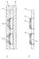
本願と関連する技術において、図17に示すようなベアチップを基板に搭載した半導体受光装置が考えられる。この半導体受光装置は、基板3上にベアチップ10を搭載し、ベアチップ上の電極パッド74と基板の引出電極78の間をワイヤーボンディングによるボンディングワイヤー20で接続する。そして、受光部12を除き、電極パッド74とボンディングワイヤー20、電極接続部を樹脂90でモールドする構造である。このような構造を形成するには、受光部12を予めなんらかのもの(例えばレジスト)で保護してから、樹脂90によるモールド行う必要がある。 In the technology related to the present application, a semiconductor light receiving device in which a bare chip as shown in FIG. 17 is mounted on a substrate can be considered. In this semiconductor light receiving device, a
図18は、受光部12の近傍の断面図である。樹脂90で囲まれた凹部の底に受光部12が配置されている。ここで周囲からの入光92があると、受光部12で反射し、樹脂90の壁面94で反射し、乱反射98を起こす。 FIG. 18 is a cross-sectional view of the vicinity of the
このような半導体受光装置に、光が入射すると、受光素子表面で反射した光が樹脂の壁面に当たって、乱反射状態となる。この乱反射光は、受光素子で再び受光され、受光素子の出力を不安定にするという問題があった。 When light is incident on such a semiconductor light receiving device, the light reflected on the surface of the light receiving element hits the wall surface of the resin and enters the irregular reflection state. The irregularly reflected light is received again by the light receiving element, and there is a problem that the output of the light receiving element becomes unstable.
具体的には、半導体受光装置が連続して併設されている場合にこの問題が生じる場合がある。すなわち、隣接する受光装置用の光が斜め方向から入射され、受光部分で全反射し、樹脂の壁面に当たって乱反射し、あたかも受光部で光を受光したかのように誤認する場合があった。 Specifically, this problem may occur when semiconductor light receiving devices are continuously provided. In other words, the light for the adjacent light receiving device is incident from an oblique direction, totally reflected at the light receiving portion, is diffusely reflected by hitting the resin wall surface, and may be misidentified as if the light is received by the light receiving portion.
また、この樹脂の壁面は、数百μm程度の大きさであり、樹脂を形成したのち機械的な加工をするのは容易でない。また上述の乱反射が生じるのを避けるために壁面94を壁面96のように傾斜させるようとフォトリソグラフィ法を駆使するのは、工程がさらに複雑になりコストが大きくなってしまう。 Moreover, the wall surface of this resin is about several hundred micrometers, and it is not easy to perform mechanical processing after forming the resin. In order to avoid the above-described irregular reflection, using the photolithography method to incline the wall surface 94 like the
これらの課題を解決すべく、本願発明者らは様々な検討を重ねた結果、本願発明にたどり着いた。以下に、実施形態について図を参照して説明する。 In order to solve these problems, the present inventors have made various studies and arrived at the present invention. Hereinafter, embodiments will be described with reference to the drawings.
(実施形態1)
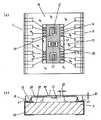
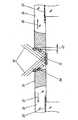
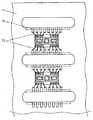
図1に実施形態1の半導体デバイス1の構成を示す。図1(a)は平面図、図1(b)は、断面図である。半導体デバイス1は、引出電極18が配置された基板3の搭載面22上に半導体素子10が搭載された構成を有する。半導体素子10は、シリコンなどの半導体基板の一方の面(一面)7上に受光部12とワイヤーボンディングのためのボンディングパッド14が形成されているものである。なお、図1(a)では説明上わかりやすくするために、断面ではない受光部12と第1の絶縁体30とにハッチングを付している。(Embodiment 1)
FIG. 1 shows the configuration of the
受光部12は一つの半導体素子10上に複数個あってもよい。図1では3つの受光部12が1つの半導体素子10に形成されている例を示す。半導体素子10上の受光部12とボンディングパッド14との位置関係は、ボンディングパッド14が半導体素子10の一面7の外周部分に配置されて、受光部12はボンディングパッド14に比べて一面7の中央部分に配置されている。本実施形態では、ボンディングパット14は左右上下に4つずつ形成されている。 A plurality of light receiving
基板3は、特に限定されるものではなく、ガラスエポキシなどのエポキシ系やフェノール系、テフロン(登録商標)系、ポリエチレン系などが好適に利用できる。基板3の搭載面22には複数の引出電極18が形成されており、その引出電極18の一部として基板側ボンディングパッド16が形成されている。基板側ボンディングパッド16は、半導体素子10側のボンディングパッド14とワイヤーボンディングするためのものである。なお、基板側ボンディングパッド16を省略して、直接引出電極18にワイヤーボンディングしてもよい。 The
引出電極18は、基板3上のみでなく基板3の側面にも形成されていてもよいし、スルーホールを介して、基板3の裏面にも形成されていてもよい。図1では、基板3の側面を回って裏面にまで形成されている場合を示す。 The
基板3と半導体素子10とは互いのボンディングパッド16,14においてボンディングワイヤー(金属細線)20によって接続される。ここで、半導体素子10側のボンディングパッド14は、基板3の表面である搭載面22より高い位置にあり、また半導体素子10の側面の部分には形成されていない。本実施形態では、ボンディングワイヤー20は基板側のボンディングパッド16から一旦上方に立ち上がり、それから半導体素子側のボンディングパッド14に接続される。これは後述する逆ワイヤー法によって作製されるからである。 The
基板3上の半導体素子10の受光部12を除いた部分およびボンディングワイヤー20は封止樹脂24によって封止されている。半導体素子10上のボンディングパッド14も封止樹脂24によって封止されている。基板3と半導体素子10との接着部分やボンディングワイヤー20の保護のためである。ただし、半導体素子10の受光部12の部分だけは、封止樹脂24に覆われていない。封止樹脂24がない方が受光感度を上げることができるからである。 A portion of the
本実施形態の半導体デバイス1では、半導体素子10上に受光部12を取り囲むように第1の絶縁体30を形成し、静電気による障害から半導体素子10を保護すると同時に封止樹脂24との境界となす。また、第1の絶縁体30は受光部12とボンディングパッド14との間に設けられている。 In the
第1の絶縁体30は、封止樹脂24を成型する際の、壁とクッションの役割を担う。すなわち、成型時において受光部12に封止樹脂24が入り込まないようにするため第1の絶縁体30を封止樹脂24の堰き止め壁とすることと、半導体素子10に直接金型の圧力をかけないようにするためである。もし、第1の絶縁体30が無いと、金型を半導体素子(受光素子)10に直接当てなければならなくなり、半導体素子10と金型のスキマから樹脂が漏れてしまう。 The
また、金型を半導体素子10に直接当てると、その圧力により半導体素子10に悪影響を及ぼす。第1の絶縁体30は、そのような悪影響を防止する。 Further, if the mold is directly applied to the
また、第1の絶縁体30はボンディングワイヤー20が十分に封止されるだけの高さ33を有している。そのため第1の絶縁体30は半導体素子10の表面から30乃至300μmの高さ33は必要である。なお、半導体デバイス1の高さを低くするためには50乃至100μmが好適である。 The
また、第1の絶縁体30は、ボンディングパッド14から所定の距離32だけ離れた位置に形成する。これは、ボンディングワイヤー20を逆ワイヤー法を用いて形成する必要があり、その際にキャピラリーと第1の絶縁体30とがぶつからないようにするためである。この距離32は、少なくとも10μmは必要である。また離しすぎると半導体素子10を大きくしなければならず、50μm以下であるのが好適である。 Further, the
また、第1の絶縁体30は受光部12の周りに開口部39を形成しており、光の種類や特性に応じて開口部39の大きさを拡大・縮小させる設計とすることが可能である。 In addition, the
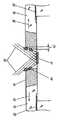
図2は、受光部12付近を拡大した断面図である。受光部12の両脇には第1の絶縁体30が存在する。ここで、半導体デバイス1の製造手順として、第1の絶縁体30を先に形成し、その後に封止樹脂24を射出形成しているため、封止樹脂24は冷却されて収縮し、引張り応力35が発生する。この引張り応力35によって、第1の絶縁体30は外側(接触してる封止樹脂24側)に引き寄せられる。その結果、受光部12から見た第1の絶縁体30の内周壁は、外側に反る。つまり、開口部39において第1の絶縁体30の内周壁は、半導体素子10の一面7から離れるに従って(上方に行くに従って)開口面積が大きくなり、テーパー形状となっている。 FIG. 2 is an enlarged cross-sectional view of the vicinity of the
ここに、入光92があった場合は、受光部12で反射した光は、反り返った第1の絶縁体30の内壁面34で乱反射を生じるため、多くの部分が受光部12の外に放出されることになる。すると、受光部12に戻る乱反射光が少なくなる。従って、半導体素子10の出力が安定する。 Here, when there is incident light 92, the light reflected by the
この第1の絶縁体30の反り40の大きさは、第1の絶縁体30の幅や高さおよび封止樹脂24の長さで変わるが、封止樹脂24の線膨張係数が10-5のオーダーであるので、反り40は数μmから10μm程度となる。なお、「反り40」は、第1の絶縁体30の内周壁が受光部12から見て外側へ傾斜しているとも言える。The size of the
次に図3を参照して、本実施形態の半導体デバイスの製造方法について説明する。 Next, with reference to FIG. 3, the manufacturing method of the semiconductor device of this embodiment is demonstrated.
基板3は、半導体素子を搭載する搭載面である基板表面5を有し、その両側に貫通孔43が形成されている。基板3からは複数の半導体デバイスが切り出されることになる。貫通孔43の内周面には、予め引出電極18が形成され、それに連続して基板表面5および基板裏面にも引出電極18が形成されている。引出電極18は、銅、アルミニウム、金、銀といった導電性の材料を用いて形成される。 The
図4では、半導体素子10を基板表面5に接着剤を用いて接着させていることが示されている。そして、図5では、受光部12の周囲に第2の絶縁体31および第1の絶縁体30を形成していることが示されている。第1の絶縁体30は、レジストを積み上げることによって形成する。第2の絶縁体31は貫通孔43近辺の基板表面5上の引出電極18の上に形成されており、封止樹脂24の成形時において金型からの樹脂漏れ防止(高さ合わせ)および、金型を受けるためのクッションの役割をする。もし、第2の絶縁体31が無い場合は、成形時に金型が引出電極18の上に乗る(接触する)ことになるので、金型と引出電極18の間の基板3にスキマが生じ、樹脂の漏れが生じてしまう。さらに、第2の絶縁体31は、金型が引出電極18に接触してその圧力で変形しないようにするためのクッションの役割も負う。 FIG. 4 shows that the
第1の絶縁体30の形成する工程には、アルカリ溶液などを用いたリンス工程が含まれているため、第2の絶縁体31は、第1の絶縁体30の形成後に印刷などの方法で形成するのが好適である。なお、第2の絶縁体31はこれ以外のタイミングで形成してもよい。例えば図3で示した引出電極18を形成した直後や、第1の絶縁体30の形成の際に同時に形成してもよい。 Since the step of forming the
図6は、第1の絶縁体30の作製方法について示している。図6(a)では、半導体素子10上にレジスト50を塗布していることが示されている。用いるレジスト50は、ポジ型の樹脂レジストを用いるのがよい。複数回の積み上げを行う場合は、感光部分が硬化するポジ型の方が作製の精度が高くなるからである。塗布方法は特に制限されるものではないが、半導体素子10上だけにレジスト50を塗布するので、印刷法が好適に利用できる。 FIG. 6 shows a method for manufacturing the
次に図6(b)を参照する。レジスト50を乾燥させ、低温で焼成することで、塗布膜を固め、ポジ用のマスク51を用いてレジスト50の一部に光52を当てて感光させる。感光用の光52が当たった部分53のレジストが硬化する。 Reference is now made to FIG. The resist 50 is dried and baked at a low temperature to harden the coating film, and a
次に図6(c)、(d)を参照する。マスク51を除去後、再びレジスト50を塗布し、焼成、感光のプロセスを繰り返す。最後に図6(e)で示すように、アルカリ溶液で未感光の部分を除去し、第1の絶縁体30を形成する。 Next, refer to FIGS. 6C and 6D. After removing the
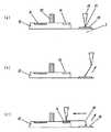
図7では、半導体素子10と基板3の引出電極18とをワイヤーボンディングによって接続していることが示されている。これによって、半導体素子10と基板3の引出電極18とはボンディングワイヤー20によって電気的に接続される。ワイヤーボンディングの方法は、ボールボンディング、ウェッジボンディングといった方法を利用することができる。ただし、ワイヤーボンディングを行う際は、逆ワイヤー方法を用いる。 FIG. 7 shows that the
図8に逆ワイヤー方法の模式図を示す。半導体素子側をファーストボンドし、基板等の接続対象をセカンドボンドするという通常のワイヤーボンディング方法とは反対の順序でワイヤーボンディングを行うのが逆ワイヤー方法である。図8(a)に、基板3の上に搭載された半導体素子10の一部を示す。半導体素子10には、受光部12とボンディングパッド14との間に第1の絶縁体30が形成されている。また、基板3上には基板側のボンディングパッド16が形成されている。ボンディングパッド16は引出電極18自体であってもよい。 FIG. 8 shows a schematic diagram of the reverse wire method. In the reverse wire method, the wire bonding is performed in the opposite order to the normal wire bonding method in which the semiconductor element side is first bonded and the connection target such as the substrate is second bonded. FIG. 8A shows a part of the
図8(a)には、キャピラリー56の先端にワイヤーの先端がボール状に形成されている状態が示されている。まずキャピラリー56をボンディングパッド16の方に移動させ、先端のボールを基板3のボンディングパッド16に接触させる。そして、熱・荷重・超音波をボールに伝えることでファーストボンド57を形成する。 FIG. 8A shows a state where the tip of the wire is formed in a ball shape at the tip of the capillary 56. First, the capillary 56 is moved toward the
図8(b)には、キャピラリー56をセカンドボンドを行う位置と反対方向の一定の高さまで斜めに引き上げていることが示されている。この場合セカンドボンドを行う位置は半導体素子10上のボンディングパット14の位置である。 FIG. 8B shows that the capillary 56 is obliquely pulled up to a certain height in the direction opposite to the position where the second bonding is performed. In this case, the position where the second bonding is performed is the position of the
図8(c)には、その後セカンドボンドを行う半導体素子10のボンディングパット14までキャピラリー56が移動していることが示されている。このように、セカンドボンドの方向と逆方向に引き上げることで、ワイヤーボンディングに必要なボンディングワイヤー20の長さを確保でき、半導体素子10の端辺とボンディングワイヤー20が接触することをさけ、切断といった欠陥の発生を抑えることが出来る。 FIG. 8C shows that the capillary 56 has moved to the
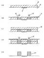
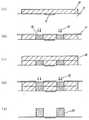
図9には、ワイヤーボンディングを行ったのち、金型45、46を基板3および第1の絶縁体30に押し当て圧力をかけながら(図9(a))、図11に示す樹脂の流れ方向47から封止樹脂24を充填する(図9(b))ことが示されている。封止樹脂24は紙面表方向から裏方向に向かって充填される。金型を基板3および第1の絶縁体30に押し当てるのは、第1の絶縁体30と金型45の隙間から封止樹脂が漏れないようにするためである。従って第1の絶縁体30から受光部12側には樹脂は充填されない。 In FIG. 9, after wire bonding, the
図10には、封止樹脂24が冷えて固まった後に金型を取り去ることが示されている。流し込まれた封止樹脂24は、冷えている第1の絶縁体30の外周部分と接触し接着する。そして、封止樹脂24自体が冷えて固まる際に封止樹脂24が収縮することで、第1の絶縁体30を受光部12から離す方向の応力35が発生する(図10(a))。第1の絶縁体30はこの応力によって、受光部12から離れていくように外側に傾斜する(図10(b))。図11には、この後基板3を切断線60で切断して半導体デバイスを得ることが示されている。なお、図11には、封止樹脂24が充填された部分と充填方向47を示した。 FIG. 10 shows that the mold is removed after the sealing
次に、半導体受光装置のバリエーションについて他の実施形態として説明する。なお、実施形態1と同じ構造部分については説明を省略する。 Next, variations of the semiconductor light receiving device will be described as another embodiment. Note that the description of the same structural portion as that of
(実施形態2)
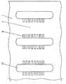
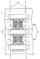
図12には、受光部12をまとめて第1の絶縁体30が一定幅でしかも受光部12を囲む構造を有している実施形態2に係る半導体デバイスが示されている。即ち、実施形態1では3つの受光部12がそれぞれ一つずつ第1の絶縁体30に取り囲まれていたが、実施形態2では、3つの受光部12をまとめて第1の絶縁体30が取り囲んでおり、2つの受光部12の間の部分には第1の絶縁体30は設けられていない。絶縁体を形成する際のマスク形状や封止樹脂の金型を比較的簡単にすることができる。(Embodiment 2)
FIG. 12 shows a semiconductor device according to the second embodiment in which the
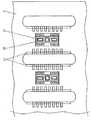
(実施形態3)
図13には、第1の絶縁体30と封止樹脂24の接続境界部分(第1の絶縁体30の外周壁)に凹凸形状を有する実施形態3に係る半導体デバイスが示されている。凹凸形状を形成することで、第1の絶縁体30と封止樹脂24との結合力を強化することができる。(Embodiment 3)
FIG. 13 shows a semiconductor device according to the third embodiment having a concavo-convex shape in a connection boundary portion (an outer peripheral wall of the first insulator 30) between the
(実施形態4)
図14には、基板3にスルーホールを形成して引出電極18の一部をスルーホールに充填した導電体によって形成した実施形態4に係る半導体デバイスが示されている。貫通電極26、27は基板3に穿たれた貫通孔の内部に銅、アルミニウム、金等の導電材料を充填したものである。裏面電極28、29は、貫通電極26、27と電気的に接合しており、銅、銀、金などの導電材料で作製されている。(Embodiment 4)
FIG. 14 shows a semiconductor device according to
(実施形態5)
図15には、基板3の裏面に第3の絶縁体61を配置した実施形態5に係る半導体デバイスが示されている。第3の絶縁体61は封止樹脂24の成形時に基板3をたわませることができるので、第1の絶縁体30によって形成された受光部12上方の開口部39をより上方が開いたテーパ形状に開かせることができる。より具体的には、第3の絶縁体61は、図10で第1の絶縁体30を外側に引っ張る応力35を助ける働きをする。なお、第3の絶縁体61は、第1の絶縁体30と同じ樹脂を用いてよい。(Embodiment 5)
FIG. 15 shows a semiconductor device according to the fifth embodiment in which the
なお、第3の絶縁体61は、裏面全体に塗布するだけでなく、2分割または3分割、若しくは適当な形状に塗布し、絶縁体を塗布しない部分を設けてもよい。絶縁体61の塗布状態を調整することで、基板3のたわみ量を調整することもできるからである。 Note that the
(実施形態6)
図16には、封止樹脂24の外周縁の角部に面取りを行った実施形態6に係る半導体デバイスのバリエーションを示す。プリント基板の集積度が高くなると、封止樹脂24の外周縁の角部が他の部品と接触する場合もあり、できるだけ不要な部分を減らすことで、他部品との干渉防止という効果がある。(Embodiment 6)
FIG. 16 shows a variation of the semiconductor device according to the sixth embodiment in which the corners of the outer peripheral edge of the sealing
図16(a)は角部への面取り加工として段36を施したものである。また図16(b)は角部への面取り加工としてテーパー37を施したものである。また図16(c)は面取り加工として角部をR形状38とした場合を示す。 FIG. 16A shows a
これらの面取りは、封止樹脂用の金型45に面取りの形状を施しておいても良いし、封止樹脂24を形成した後、切削加工や研削加工によって成形してもよい。 These chamfers may be formed by chamfering the sealing
本発明は、受光部分をむき出しにしたベアチップを搭載した半導体デバイス等に利用する事が出来る。 The present invention can be used for a semiconductor device mounted with a bare chip with a light receiving portion exposed.
本発明は、半導体デバイスおよび半導体デバイスの製造方法に関し、特に受光部を備えた半導体素子を基板に搭載した半導体デバイスおよび半導体デバイスの製造方法に関するものである。 The present invention relates to a semiconductor device and a method for manufacturing the semiconductor device, and more particularly to a semiconductor device in which a semiconductor element having a light receiving portion is mounted on a substrate and a method for manufacturing the semiconductor device.
半導体受光装置は、電極を配設した基板上にフォトセンサチップを配置し、それを透明保護層で覆う構成を有する。これは、電極パッド、ワイヤーや受光部といった部分を、外気に含まれる水分による腐食や、塵埃から保護するためである。 The semiconductor light-receiving device has a configuration in which a photosensor chip is disposed on a substrate on which electrodes are disposed, and is covered with a transparent protective layer. This is for protecting parts such as the electrode pad, the wire, and the light receiving part from corrosion caused by moisture contained in the outside air and dust.
しかし、近年、電子機器の小型化によって、半導体受光装置を含む部品が小型化し、電子機器の部品の一部に組み込まれ、一体化した部品となる場合が多くなってきている。このような一体化部品は、外形部分を樹脂で密封されている場合が多く、水分や塵埃が入り込む隙がほとんどない。 However, in recent years, due to miniaturization of electronic devices, components including a semiconductor light receiving device have been miniaturized and are often incorporated into a part of electronic device components to become integrated components. Such an integrated part often has an outer portion sealed with a resin, and there is almost no space for moisture or dust to enter.
また、ハードディスクドライブ装置においては、ドライブ装置自体が密封状態にあり、内部は、水分や塵埃の非常に少ない清浄な気体で満たされている。 Further, in the hard disk drive device, the drive device itself is in a sealed state, and the inside is filled with a clean gas with very little moisture and dust.
このような密封状態にある半導体受光装置では、上記のように透明保護層で覆う必要はなく、受光部をむき出しにしてもよい。受光部をむき出しにした半導体受光装置は、受光感度が向上するという効果を得ることができる。なお、受光部をむき出しにした半導体チップをベアチップと呼ぶ。 In the semiconductor light-receiving device in such a sealed state, it is not necessary to cover with the transparent protective layer as described above, and the light-receiving portion may be exposed. The semiconductor light receiving device with the light receiving portion exposed can obtain an effect that the light receiving sensitivity is improved. A semiconductor chip with the light receiving portion exposed is called a bare chip.
特許文献1に開示されている半導体受光装置の製造方法は、受光部の上にフォトリソグラフィ法によってレジストを載せて、その後樹脂をモールドしてから、そのレジストを除去することによってベアチップとなす。 In the method of manufacturing a semiconductor light receiving device disclosed in
受光部上の透明保護層を省いた半導体受光装置は、基板とフォトセンサチップを接続するための端子部分などは封止樹脂でモールドされており、受光部分だけが露出している。すなわち、樹脂体で形成された凹部の底に受光部分が形成されている。 In the semiconductor light receiving device without the transparent protective layer on the light receiving portion, the terminal portion for connecting the substrate and the photo sensor chip is molded with sealing resin, and only the light receiving portion is exposed. That is, the light receiving portion is formed at the bottom of the recess formed of the resin body.
このような半導体受光装置において、樹脂体で形成された凹部の壁面が反射した光が受光部分に入射すると、受光素子面で入射光が反射し、受光素子表面で反射した光が封止樹脂の壁面に当たって、乱反射状態となる。この乱反射光は、受光素子で再び受光され、受光素子の出力を不安定にするという問題があった。 In such a semiconductor light receiving device, when the light reflected by the wall surface of the recess formed of the resin body enters the light receiving portion, the incident light is reflected by the surface of the light receiving element, and the light reflected by the surface of the light receiving element is reflected by the sealing resin. When it hits the wall surface, it becomes a diffuse reflection state. The irregularly reflected light is received again by the light receiving element, and there is a problem that the output of the light receiving element becomes unstable.
上記課題を解決するために、本発明の半導体デバイスは、半導体素子と、該半導体素子を搭載した基板とを備えた半導体デバイスであって、前記半導体素子は、一面に受光部とボンディングパッドとを備え、該一面の裏面側が前記基板に搭載されており、前記半導体素子を搭載する側の面である前記基板の搭載面には引出電極が形成されており、前記ボンディングパッドと前記引出電極とは金属細線によって接続されており、前記半導体素子の前記一面には、前記受光部と前記ボンディングパッドとの間に存するともに該受光部を取り囲む第1の絶縁体が設けられており、前記ボンディングパッドと前記金属細線とは封止樹脂によって封止されており、前記半導体素子の前記一面において前記第1の絶縁体の外周は前記封止樹脂と接触しており、前記受光部に臨み且つ該受光部を取り囲む前記第1の絶縁体の内周壁は、前記半導体素子の前記一面から離れるに従って開口面積が広がるテーパー形状を有している構成とした。 In order to solve the above problems, a semiconductor device of the present invention is a semiconductor device including a semiconductor element and a substrate on which the semiconductor element is mounted, and the semiconductor element has a light receiving portion and a bonding pad on one surface. Provided, the back surface side of the one surface is mounted on the substrate, an extraction electrode is formed on the mounting surface of the substrate, which is a surface on which the semiconductor element is mounted, and the bonding pad and the extraction electrode are The one surface of the semiconductor element is provided with a first insulator that exists between the light receiving portion and the bonding pad and surrounds the light receiving portion, and is connected to the bonding pad, The fine metal wire is sealed with a sealing resin, and an outer periphery of the first insulator is in contact with the sealing resin on the one surface of the semiconductor element. , The inner peripheral wall of said first insulator surrounding a and the light receiving portion faces the light receiving portion, and configured to have a tapered shape that the opening area widens as the distance from the one surface of the semiconductor element.
本発明の半導体デバイスは、受光部の周囲に絶縁体の枠体を形成し、その枠体の外側に封止樹脂を形成させたので、封止樹脂の硬化時に枠体が外側に引っ張られ、枠体の壁面が斜めに形成される。したがって受光部で反射した不要な光が壁面で乱反射しても、半導体デバイスが誤動作をすることがなくなるという効果を得ることができる。 In the semiconductor device of the present invention, an insulating frame is formed around the light receiving portion, and the sealing resin is formed outside the frame, so the frame is pulled outward when the sealing resin is cured, The wall surface of the frame is formed obliquely. Therefore, it is possible to obtain an effect that the semiconductor device does not malfunction even if unnecessary light reflected by the light receiving portion is irregularly reflected by the wall surface.
本願と関連する技術において、図17に示すようなベアチップを基板に搭載した半導体受光装置が考えられる。この半導体受光装置は、基板3上にベアチップ10を搭載し、ベアチップ上の電極パッド74と基板の引出電極78の間をワイヤーボンディングによるボンディングワイヤー20で接続する。そして、受光部12を除き、電極パッド74とボンディングワイヤー20、電極接続部を樹脂90でモールドする構造である。このような構造を形成するには、受光部12を予めなんらかのもの(例えばレジスト)で保護してから、樹脂90によるモールド行う必要がある。 In the technology related to the present application, a semiconductor light receiving device in which a bare chip as shown in FIG. 17 is mounted on a substrate can be considered. In this semiconductor light receiving device, a
図18は、受光部12の近傍の断面図である。樹脂90で囲まれた凹部の底に受光部12が配置されている。ここで周囲からの入光92があると、受光部12で反射し、樹脂90の壁面94で反射し、乱反射98を起こす。 FIG. 18 is a cross-sectional view of the vicinity of the
このような半導体受光装置に、光が入射すると、受光素子表面で反射した光が樹脂の壁面に当たって、乱反射状態となる。この乱反射光は、受光素子で再び受光され、受光素子の出力を不安定にするという問題があった。 When light is incident on such a semiconductor light receiving device, the light reflected on the surface of the light receiving element hits the wall surface of the resin and enters the irregular reflection state. The irregularly reflected light is received again by the light receiving element, and there is a problem that the output of the light receiving element becomes unstable.
具体的には、半導体受光装置が連続して併設されている場合にこの問題が生じる場合がある。すなわち、隣接する受光装置用の光が斜め方向から入射され、受光部分で全反射し、樹脂の壁面に当たって乱反射し、あたかも受光部で光を受光したかのように誤認する場合があった。 Specifically, this problem may occur when semiconductor light receiving devices are continuously provided. In other words, the light for the adjacent light receiving device is incident from an oblique direction, totally reflected at the light receiving portion, is diffusely reflected by hitting the resin wall surface, and may be misidentified as if the light is received by the light receiving portion.
また、この樹脂の壁面は、数百μm程度の大きさであり、樹脂を形成したのち機械的な加工をするのは容易でない。また上述の乱反射が生じるのを避けるために壁面94を壁面96のように傾斜させるようとフォトリソグラフィ法を駆使するのは、工程がさらに複雑になりコストが大きくなってしまう。 Moreover, the wall surface of this resin is about several hundred micrometers, and it is not easy to perform mechanical processing after forming the resin. In order to avoid the above-described irregular reflection, using the photolithography method to incline the wall surface 94 like the
これらの課題を解決すべく、本願発明者らは様々な検討を重ねた結果、本願発明にたどり着いた。以下に、実施形態について図を参照して説明する。 In order to solve these problems, the present inventors have made various studies and arrived at the present invention. Hereinafter, embodiments will be described with reference to the drawings.
(実施形態1)
図1に実施形態1の半導体デバイス1の構成を示す。図1(a)は平面図、図1(b)は、断面図である。半導体デバイス1は、引出電極18が配置された基板3の搭載面22上に半導体素子10が搭載された構成を有する。半導体素子10は、シリコンなどの半導体基板の一方の面(一面)7上に受光部12とワイヤーボンディングのためのボンディングパッド14が形成されているものである。なお、図1(a)では説明上わかりやすくするために、断面ではない受光部12と第1の絶縁体30とにハッチングを付している。(Embodiment 1)
FIG. 1 shows the configuration of the
受光部12は一つの半導体素子10上に複数個あってもよい。図1では3つの受光部12が1つの半導体素子10に形成されている例を示す。半導体素子10上の受光部12とボンディングパッド14との位置関係は、ボンディングパッド14が半導体素子10の一面7の外周部分に配置されて、受光部12はボンディングパッド14に比べて一面7の中央部分に配置されている。本実施形態では、ボンディングパット14は左右上下に4つずつ形成されている。 A plurality of light receiving
基板3は、特に限定されるものではなく、ガラスエポキシなどのエポキシ系やフェノール系、テフロン(登録商標)系、ポリエチレン系などが好適に利用できる。基板3の搭載面22には複数の引出電極18が形成されており、その引出電極18の一部として基板側ボンディングパッド16が形成されている。基板側ボンディングパッド16は、半導体素子10側のボンディングパッド14とワイヤーボンディングするためのものである。なお、基板側ボンディングパッド16を省略して、直接引出電極18にワイヤーボンディングしてもよい。 The
引出電極18は、基板3上のみでなく基板3の側面にも形成されていてもよいし、スルーホールを介して、基板3の裏面にも形成されていてもよい。図1では、基板3の側面を回って裏面にまで形成されている場合を示す。 The
基板3と半導体素子10とは互いのボンディングパッド16,14においてボンディングワイヤー(金属細線)20によって接続される。ここで、半導体素子10側のボンディングパッド14は、基板3の表面である搭載面22より高い位置にあり、また半導体素子10の側面の部分には形成されていない。本実施形態では、ボンディングワイヤー20は基板側のボンディングパッド16から一旦上方に立ち上がり、それから半導体素子側のボンディングパッド14に接続される。これは後述する逆ワイヤー法によって作製されるからである。 The
基板3上の半導体素子10の受光部12を除いた部分およびボンディングワイヤー20は封止樹脂24によって封止されている。半導体素子10上のボンディングパッド14も封止樹脂24によって封止されている。基板3と半導体素子10との接着部分やボンディングワイヤー20の保護のためである。ただし、半導体素子10の受光部12の部分だけは、封止樹脂24に覆われていない。封止樹脂24がない方が受光感度を上げることができるからである。 A portion of the
本実施形態の半導体デバイス1では、半導体素子10上に受光部12を取り囲むように第1の絶縁体30を形成し、静電気による障害から半導体素子10を保護すると同時に封止樹脂24との境界となす。また、第1の絶縁体30は受光部12とボンディングパッド14との間に設けられている。 In the
第1の絶縁体30は、封止樹脂24を成型する際の、壁とクッションの役割を担う。すなわち、成型時において受光部12に封止樹脂24が入り込まないようにするため第1の絶縁体30を封止樹脂24の堰き止め壁とすることと、半導体素子10に直接金型の圧力をかけないようにするためである。もし、第1の絶縁体30が無いと、金型を半導体素子(受光素子)10に直接当てなければならなくなり、半導体素子10と金型のスキマから樹脂が漏れてしまう。 The
また、金型を半導体素子10に直接当てると、その圧力により半導体素子10に悪影響を及ぼす。第1の絶縁体30は、そのような悪影響を防止する。 Further, if the mold is directly applied to the
また、第1の絶縁体30はボンディングワイヤー20が十分に封止されるだけの高さ33を有している。そのため第1の絶縁体30は半導体素子10の表面から30乃至300μmの高さ33は必要である。なお、半導体デバイス1の高さを低くするためには50乃至100μmが好適である。 The
また、第1の絶縁体30は、ボンディングパッド14から所定の距離32だけ離れた位置に形成する。これは、ボンディングワイヤー20を逆ワイヤー法を用いて形成する必要があり、その際にキャピラリーと第1の絶縁体30とがぶつからないようにするためである。この距離32は、少なくとも10μmは必要である。また離しすぎると半導体素子10を大きくしなければならず、50μm以下であるのが好適である。 Further, the
また、第1の絶縁体30は受光部12の周りに開口部39を形成しており、光の種類や特性に応じて開口部39の大きさを拡大・縮小させる設計とすることが可能である。 In addition, the
図2は、受光部12付近を拡大した断面図である。受光部12の両脇には第1の絶縁体30が存在する。ここで、半導体デバイス1の製造手順として、第1の絶縁体30を先に形成し、その後に封止樹脂24を射出形成しているため、封止樹脂24は冷却されて収縮し、引張り応力35が発生する。この引張り応力35によって、第1の絶縁体30は外側(接触してる封止樹脂24側)に引き寄せられる。その結果、受光部12から見た第1の絶縁体30の内周壁は、外側に反る。つまり、開口部39において第1の絶縁体30の内周壁は、半導体素子10の一面7から離れるに従って(上方に行くに従って)開口面積が大きくなり、テーパー形状となっている。 FIG. 2 is an enlarged cross-sectional view of the vicinity of the
ここに、入光92があった場合は、受光部12で反射した光は、反り返った第1の絶縁体30の内壁面34で乱反射を生じるため、多くの部分が受光部12の外に放出されることになる。すると、受光部12に戻る乱反射光が少なくなる。従って、半導体素子10の出力が安定する。 Here, when there is incident light 92, the light reflected by the
この第1の絶縁体30の反り40の大きさは、第1の絶縁体30の幅や高さおよび封止樹脂24の長さで変わるが、封止樹脂24の線膨張係数が10-5のオーダーであるので、反り40は数μmから10μm程度となる。なお、「反り40」は、第1の絶縁体30の内周壁が受光部12から見て外側へ傾斜しているとも言える。The size of the
次に図3を参照して、本実施形態の半導体デバイスの製造方法について説明する。 Next, with reference to FIG. 3, the manufacturing method of the semiconductor device of this embodiment is demonstrated.
基板3は、半導体素子を搭載する搭載面である基板表面5を有し、その両側に貫通孔43が形成されている。基板3からは複数の半導体デバイスが切り出されることになる。貫通孔43の内周面には、予め引出電極18が形成され、それに連続して基板表面5および基板裏面にも引出電極18が形成されている。引出電極18は、銅、アルミニウム、金、銀といった導電性の材料を用いて形成される。 The
図4では、半導体素子10を基板表面5に接着剤を用いて接着させていることが示されている。そして、図5では、受光部12の周囲に第2の絶縁体31および第1の絶縁体30を形成していることが示されている。第1の絶縁体30は、レジストを積み上げることによって形成する。第2の絶縁体31は貫通孔43近辺の基板表面5上の引出電極18の上に形成されており、封止樹脂24の成形時において金型からの樹脂漏れ防止(高さ合わせ)および、金型を受けるためのクッションの役割をする。もし、第2の絶縁体31が無い場合は、成形時に金型が引出電極18の上に乗る(接触する)ことになるので、金型と引出電極18の間の基板3にスキマが生じ、樹脂の漏れが生じてしまう。さらに、第2の絶縁体31は、金型が引出電極18に接触してその圧力で変形しないようにするためのクッションの役割も負う。 FIG. 4 shows that the
第1の絶縁体30の形成する工程には、アルカリ溶液などを用いたリンス工程が含まれているため、第2の絶縁体31は、第1の絶縁体30の形成後に印刷などの方法で形成するのが好適である。なお、第2の絶縁体31はこれ以外のタイミングで形成してもよい。例えば図3で示した引出電極18を形成した直後や、第1の絶縁体30の形成の際に同時に形成してもよい。 Since the step of forming the
図6は、第1の絶縁体30の作製方法について示している。図6(a)では、半導体素子10上にレジスト50を塗布していることが示されている。用いるレジスト50は、ポジ型の樹脂レジストを用いるのがよい。複数回の積み上げを行う場合は、感光部分が硬化するポジ型の方が作製の精度が高くなるからである。塗布方法は特に制限されるものではないが、半導体素子10上だけにレジスト50を塗布するので、印刷法が好適に利用できる。 FIG. 6 shows a method for manufacturing the
次に図6(b)を参照する。レジスト50を乾燥させ、低温で焼成することで、塗布膜を固め、ポジ用のマスク51を用いてレジスト50の一部に光52を当てて感光させる。感光用の光52が当たった部分53のレジストが硬化する。 Reference is now made to FIG. The resist 50 is dried and baked at a low temperature to harden the coating film, and a
次に図6(c)、(d)を参照する。マスク51を除去後、再びレジスト50を塗布し、焼成、感光のプロセスを繰り返す。最後に図6(e)で示すように、アルカリ溶液で未感光の部分を除去し、第1の絶縁体30を形成する。 Next, refer to FIGS. 6C and 6D. After removing the
図7では、半導体素子10と基板3の引出電極18とをワイヤーボンディングによって接続していることが示されている。これによって、半導体素子10と基板3の引出電極18とはボンディングワイヤー20によって電気的に接続される。ワイヤーボンディングの方法は、ボールボンディング、ウェッジボンディングといった方法を利用することができる。ただし、ワイヤーボンディングを行う際は、逆ワイヤー方法を用いる。 FIG. 7 shows that the
図8に逆ワイヤー方法の模式図を示す。半導体素子側をファーストボンドし、基板等の接続対象をセカンドボンドするという通常のワイヤーボンディング方法とは反対の順序でワイヤーボンディングを行うのが逆ワイヤー方法である。図8(a)に、基板3の上に搭載された半導体素子10の一部を示す。半導体素子10には、受光部12とボンディングパッド14との間に第1の絶縁体30が形成されている。また、基板3上には基板側のボンディングパッド16が形成されている。ボンディングパッド16は引出電極18自体であってもよい。 FIG. 8 shows a schematic diagram of the reverse wire method. In the reverse wire method, the wire bonding is performed in the opposite order to the normal wire bonding method in which the semiconductor element side is first bonded and the connection target such as the substrate is second bonded. FIG. 8A shows a part of the
図8(a)には、キャピラリー56の先端にワイヤーの先端がボール状に形成されている状態が示されている。まずキャピラリー56をボンディングパッド16の方に移動させ、先端のボールを基板3のボンディングパッド16に接触させる。そして、熱・荷重・超音波をボールに伝えることでファーストボンド57を形成する。 FIG. 8A shows a state where the tip of the wire is formed in a ball shape at the tip of the capillary 56. First, the capillary 56 is moved toward the
図8(b)には、キャピラリー56をセカンドボンドを行う位置と反対方向の一定の高さまで斜めに引き上げていることが示されている。この場合セカンドボンドを行う位置は半導体素子10上のボンディングパット14の位置である。 FIG. 8B shows that the capillary 56 is obliquely pulled up to a certain height in the direction opposite to the position where the second bonding is performed. In this case, the position where the second bonding is performed is the position of the
図8(c)には、その後セカンドボンドを行う半導体素子10のボンディングパット14までキャピラリー56が移動していることが示されている。このように、セカンドボンドの方向と逆方向に引き上げることで、ワイヤーボンディングに必要なボンディングワイヤー20の長さを確保でき、半導体素子10の端辺とボンディングワイヤー20が接触することをさけ、切断といった欠陥の発生を抑えることが出来る。 FIG. 8C shows that the capillary 56 has moved to the
図9には、ワイヤーボンディングを行ったのち、金型45、46を基板3および第1の絶縁体30に押し当て圧力をかけながら(図9(a))、図11に示す樹脂の流れ方向47から封止樹脂24を充填する(図9(b))ことが示されている。封止樹脂24は紙面表方向から裏方向に向かって充填される。金型を基板3および第1の絶縁体30に押し当てるのは、第1の絶縁体30と金型45の隙間から封止樹脂が漏れないようにするためである。従って第1の絶縁体30から受光部12側には樹脂は充填されない。 In FIG. 9, after wire bonding, the
図10には、封止樹脂24が冷えて固まった後に金型を取り去ることが示されている。流し込まれた封止樹脂24は、冷えている第1の絶縁体30の外周部分と接触し接着する。そして、封止樹脂24自体が冷えて固まる際に封止樹脂24が収縮することで、第1の絶縁体30を受光部12から離す方向の応力35が発生する(図10(a))。第1の絶縁体30はこの応力によって、受光部12から離れていくように外側に傾斜する(図10(b))。図11には、この後基板3を切断線60で切断して半導体デバイスを得ることが示されている。なお、図11には、封止樹脂24が充填された部分と充填方向47を示した。 FIG. 10 shows that the mold is removed after the sealing
次に、半導体受光装置のバリエーションについて他の実施形態として説明する。なお、実施形態1と同じ構造部分については説明を省略する。 Next, variations of the semiconductor light receiving device will be described as another embodiment. Note that the description of the same structural portion as that of
(実施形態2)
図12には、受光部12をまとめて第1の絶縁体30が一定幅でしかも受光部12を囲む構造を有している実施形態2に係る半導体デバイスが示されている。即ち、実施形態1では3つの受光部12がそれぞれ一つずつ第1の絶縁体30に取り囲まれていたが、実施形態2では、3つの受光部12をまとめて第1の絶縁体30が取り囲んでおり、2つの受光部12の間の部分には第1の絶縁体30は設けられていない。絶縁体を形成する際のマスク形状や封止樹脂の金型を比較的簡単にすることができる。(Embodiment 2)
FIG. 12 shows a semiconductor device according to the second embodiment in which the
(実施形態3)
図13には、第1の絶縁体30と封止樹脂24の接続境界部分(第1の絶縁体30の外周壁)に凹凸形状を有する実施形態3に係る半導体デバイスが示されている。凹凸形状を形成することで、第1の絶縁体30と封止樹脂24との結合力を強化することができる。(Embodiment 3)
FIG. 13 shows a semiconductor device according to the third embodiment having a concavo-convex shape in a connection boundary portion (an outer peripheral wall of the first insulator 30) between the
(実施形態4)
図14には、基板3にスルーホールを形成して引出電極18の一部をスルーホールに充填した導電体によって形成した実施形態4に係る半導体デバイスが示されている。貫通電極26、27は基板3に穿たれた貫通孔の内部に銅、アルミニウム、金等の導電材料を充填したものである。裏面電極28、29は、貫通電極26、27と電気的に接合しており、銅、銀、金などの導電材料で作製されている。(Embodiment 4)
FIG. 14 shows a semiconductor device according to
(実施形態5)
図15には、基板3の裏面に第3の絶縁体61を配置した実施形態5に係る半導体デバイスが示されている。第3の絶縁体61は封止樹脂24の成形時に基板3をたわませることができるので、第1の絶縁体30によって形成された受光部12上方の開口部39をより上方が開いたテーパ形状に開かせることができる。より具体的には、第3の絶縁体61は、図10で第1の絶縁体30を外側に引っ張る応力35を助ける働きをする。なお、第3の絶縁体61は、第1の絶縁体30と同じ樹脂を用いてよい。(Embodiment 5)
FIG. 15 shows a semiconductor device according to the fifth embodiment in which the
なお、第3の絶縁体61は、裏面全体に塗布するだけでなく、2分割または3分割、若しくは適当な形状に塗布し、絶縁体を塗布しない部分を設けてもよい。絶縁体61の塗布状態を調整することで、基板3のたわみ量を調整することもできるからである。 Note that the
(実施形態6)
図16には、封止樹脂24の外周縁の角部に面取りを行った実施形態6に係る半導体デバイスのバリエーションを示す。プリント基板の集積度が高くなると、封止樹脂24の外周縁の角部が他の部品と接触する場合もあり、できるだけ不要な部分を減らすことで、他部品との干渉防止という効果がある。(Embodiment 6)
FIG. 16 shows a variation of the semiconductor device according to the sixth embodiment in which the corners of the outer peripheral edge of the sealing
図16(a)は角部への面取り加工として段36を施したものである。また図16(b)は角部への面取り加工としてテーパー37を施したものである。また図16(c)は面取り加工として角部をR形状38とした場合を示す。 FIG. 16A shows a
これらの面取りは、封止樹脂用の金型45に面取りの形状を施しておいても良いし、封止樹脂24を形成した後、切削加工や研削加工によって成形してもよい。 These chamfers may be formed by chamfering the sealing
本発明は、受光部分をむき出しにしたベアチップを搭載した半導体デバイス等に利用する事が出来る。 The present invention can be used for a semiconductor device mounted with a bare chip with a light receiving portion exposed.
1 半導体デバイス
3 基板
5 基板表面
7 一面
10 半導体素子
12 受光部
14 ボンディングパッド
16 ボンディングパッド
18 引出電極
20 ボンディングワイヤー(金属細線)
22 搭載面
24 封止樹脂
26,27 貫通電極
28,29 裏面電極
30 第1の絶縁体
31 第2の絶縁体
34 壁面
39 開口部
43 貫通孔
61 第3の絶縁体DESCRIPTION OF
22
Claims (9)
Translated fromJapanese前記半導体素子は、一面に受光部とボンディングパッドとを備え、該一面の裏面側が前記基板に搭載されており、
前記半導体素子を搭載する側の面である前記基板の搭載面には引出電極が形成されており、
前記ボンディングパッドと前記引出電極とは金属細線によって接続されており、
前記半導体素子の前記一面には、前記受光部と前記ボンディングパッドとの間に存するともに該受光部を取り囲む第1の絶縁体が設けられており、
前記ボンディングパッドと前記金属細線とは封止樹脂によって封止されており、
前記半導体素子の前記一面において前記第1の絶縁体の外周は前記封止樹脂と接触しており、
前記受光部に臨み且つ該受光部を取り囲む前記第1の絶縁体の内周壁は、前記半導体素子の前記一面から離れるに従って開口面積が広がるテーパー形状を有している、半導体デバイス。A semiconductor device comprising a semiconductor element and a substrate on which the semiconductor element is mounted,
The semiconductor element includes a light receiving portion and a bonding pad on one surface, and the back surface side of the one surface is mounted on the substrate,
An extraction electrode is formed on the mounting surface of the substrate, which is the surface on which the semiconductor element is mounted,
The bonding pad and the extraction electrode are connected by a thin metal wire,
The one surface of the semiconductor element is provided with a first insulator that exists between the light receiving portion and the bonding pad and surrounds the light receiving portion,
The bonding pad and the metal fine wire are sealed with a sealing resin,
An outer periphery of the first insulator is in contact with the sealing resin on the one surface of the semiconductor element;
An inner peripheral wall of the first insulator that faces the light receiving portion and surrounds the light receiving portion has a tapered shape in which an opening area increases as the distance from the one surface of the semiconductor element increases.
前記搭載面の外周において前記引出電極上に第2の絶縁体が形成されていることを特徴とする、請求項1または2のいずれかの請求項に記載された半導体デバイス。The extraction electrode extends to an outer peripheral edge of the mounting surface;
3. The semiconductor device according to claim 1, wherein a second insulator is formed on the extraction electrode at an outer periphery of the mounting surface. 4.
前記半導体素子の受光部を取り囲むように該受光部と前記ボンディングパッドとの間に第1の絶縁体を該半導体素子上に設ける工程と、
前記ボンディングパッドと前記引出電極とを金属細線で接続する工程と、
前記ボンディングパッドと前記金属細線とを封止樹脂で封止するとともに前記第1の絶縁体の外周壁部に該封止樹脂を接触させる工程と、
を含み、
前記封止樹脂の硬化時の応力によって前記絶縁体の内周壁は上部が前記外周壁側に傾斜していることを特徴とする半導体デバイスの製造方法。Mounting a semiconductor element having a light receiving portion and a bonding pad on a substrate having an extraction electrode;
Providing a first insulator on the semiconductor element between the light receiving portion and the bonding pad so as to surround the light receiving portion of the semiconductor element;
Connecting the bonding pad and the extraction electrode with a fine metal wire;
Sealing the bonding pad and the fine metal wire with a sealing resin and bringing the sealing resin into contact with an outer peripheral wall of the first insulator;
Including
The method of manufacturing a semiconductor device, wherein an upper portion of the inner peripheral wall of the insulator is inclined to the outer peripheral wall side due to stress during curing of the sealing resin.
Applications Claiming Priority (3)
| Application Number | Priority Date | Filing Date | Title |
|---|---|---|---|
| JP2008060668 | 2008-03-11 | ||
| JP2008060668 | 2008-03-11 | ||
| PCT/JP2009/000862WO2009113262A1 (en) | 2008-03-11 | 2009-02-26 | Semiconductor device and semiconductor device manufacturing method |
Publications (1)
| Publication Number | Publication Date |
|---|---|
| JPWO2009113262A1true JPWO2009113262A1 (en) | 2011-07-21 |
Family
ID=41064936
Family Applications (1)
| Application Number | Title | Priority Date | Filing Date |
|---|---|---|---|
| JP2010502706APendingJPWO2009113262A1 (en) | 2008-03-11 | 2009-02-26 | Semiconductor device and manufacturing method of semiconductor device |
Country Status (4)
| Country | Link |
|---|---|
| US (1) | US8274125B2 (en) |
| JP (1) | JPWO2009113262A1 (en) |
| CN (1) | CN101960608A (en) |
| WO (1) | WO2009113262A1 (en) |
Families Citing this family (5)
| Publication number | Priority date | Publication date | Assignee | Title |
|---|---|---|---|---|
| JP6227223B2 (en)* | 2012-03-30 | 2017-11-08 | 富士通テン株式会社 | Semiconductor device and manufacturing method of semiconductor device |
| JP6353354B2 (en)* | 2014-12-12 | 2018-07-04 | ルネサスエレクトロニクス株式会社 | Imaging device and manufacturing method thereof |
| EP3672220B1 (en)* | 2017-08-18 | 2024-06-05 | Ningbo Sunny Opotech Co., Ltd. | Photosensitive assembly, imaging module, intelligent terminal, and method and mould for manufacturing photosensitive assembly |
| JP7273297B2 (en)* | 2019-06-28 | 2023-05-15 | 日亜化学工業株式会社 | Light-emitting module and method for manufacturing light-emitting module |
| JP7556080B2 (en)* | 2023-03-03 | 2024-09-25 | セイコーNpc株式会社 | Optical device and method for manufacturing optical device |
Citations (3)
| Publication number | Priority date | Publication date | Assignee | Title |
|---|---|---|---|---|
| JP2002222821A (en)* | 2001-01-29 | 2002-08-09 | Sony Corp | Resin frame forming device and method therefor |
| JP2007189182A (en)* | 2005-03-09 | 2007-07-26 | Pioneer Electronic Corp | Light sensing semiconductor device and its manufacturing method |
| JP2009081346A (en)* | 2007-09-27 | 2009-04-16 | Panasonic Corp | Optical device and manufacturing method thereof |
Family Cites Families (14)
| Publication number | Priority date | Publication date | Assignee | Title |
|---|---|---|---|---|
| US5962810A (en)* | 1997-09-09 | 1999-10-05 | Amkor Technology, Inc. | Integrated circuit package employing a transparent encapsulant |
| JP2002076154A (en)* | 2000-08-23 | 2002-03-15 | Kyocera Corp | Semiconductor device |
| US6653723B2 (en)* | 2002-03-09 | 2003-11-25 | Fujitsu Limited | System for providing an open-cavity low profile encapsulated semiconductor package |
| US7122874B2 (en)* | 2004-04-12 | 2006-10-17 | Optopac, Inc. | Electronic package having a sealing structure on predetermined area, and the method thereof |
| JP3936365B2 (en)* | 2004-09-14 | 2007-06-27 | ソニーケミカル&インフォメーションデバイス株式会社 | Functional element mounting module and manufacturing method thereof |
| TWI251886B (en)* | 2004-11-03 | 2006-03-21 | Advanced Semiconductor Eng | Sensor chip for defining molding exposed region and method for manufacturing the same |
| TWM266539U (en)* | 2004-11-05 | 2005-06-01 | Altus Technology Inc | Integrate circuit chip encapsulation |
| JP4324081B2 (en)* | 2004-11-22 | 2009-09-02 | パナソニック株式会社 | Optical device |
| US7227236B1 (en)* | 2005-04-26 | 2007-06-05 | Amkor Technology, Inc. | Image sensor package and its manufacturing method |
| US7745897B2 (en)* | 2005-05-27 | 2010-06-29 | Aptina Imaging Corporation | Methods for packaging an image sensor and a packaged image sensor |
| JP4382030B2 (en)* | 2005-11-15 | 2009-12-09 | 富士通マイクロエレクトロニクス株式会社 | Semiconductor device and manufacturing method thereof |
| JP2007150038A (en)* | 2005-11-29 | 2007-06-14 | Tdk Corp | Optical semiconductor device and method for fabrication thereof |
| KR101144489B1 (en)* | 2005-12-23 | 2012-05-11 | 엘지이노텍 주식회사 | Pakage of light emitting diode |
| TWI289916B (en)* | 2006-03-24 | 2007-11-11 | Advanced Semiconductor Eng | Chip package and package process thereof |
- 2009
- 2009-02-26WOPCT/JP2009/000862patent/WO2009113262A1/enactiveApplication Filing
- 2009-02-26USUS12/918,023patent/US8274125B2/ennot_activeExpired - Fee Related
- 2009-02-26JPJP2010502706Apatent/JPWO2009113262A1/enactivePending
- 2009-02-26CNCN200980107640XApatent/CN101960608A/enactivePending
Patent Citations (3)
| Publication number | Priority date | Publication date | Assignee | Title |
|---|---|---|---|---|
| JP2002222821A (en)* | 2001-01-29 | 2002-08-09 | Sony Corp | Resin frame forming device and method therefor |
| JP2007189182A (en)* | 2005-03-09 | 2007-07-26 | Pioneer Electronic Corp | Light sensing semiconductor device and its manufacturing method |
| JP2009081346A (en)* | 2007-09-27 | 2009-04-16 | Panasonic Corp | Optical device and manufacturing method thereof |
Also Published As
| Publication number | Publication date |
|---|---|
| CN101960608A (en) | 2011-01-26 |
| WO2009113262A1 (en) | 2009-09-17 |
| US20110001208A1 (en) | 2011-01-06 |
| US8274125B2 (en) | 2012-09-25 |
Similar Documents
| Publication | Publication Date | Title |
|---|---|---|
| JP5746919B2 (en) | Semiconductor package | |
| CN101582435B (en) | Packaging structure for image sensing wafer and camera module applying same | |
| JP4380718B2 (en) | Manufacturing method of semiconductor device | |
| CN100533712C (en) | Photoelectric element chip and manufacturing method thereof | |
| US8120128B2 (en) | Optical device | |
| JP2010016030A (en) | Electronic component | |
| CN100433339C (en) | Solid-state imaging device and method for producing the same | |
| JP2008277325A (en) | Semiconductor device and manufacturing method of semiconductor device | |
| EP3570326B1 (en) | Sensor package structure | |
| CN115810605A (en) | Lead frame, semiconductor device, inspection method, and lead frame manufacturing method | |
| US20080277775A1 (en) | Ultra-thin near-hermetic package based on rainier | |
| CN113519058A (en) | semiconductor device | |
| CN112635505A (en) | Packaging structure and packaging method | |
| JPWO2009113262A1 (en) | Semiconductor device and manufacturing method of semiconductor device | |
| WO2014061204A1 (en) | Semiconductor device and method for manufacturing same | |
| CN101241920A (en) | Optical device and manufacturing method thereof | |
| JP2010252164A (en) | Solid-state imaging device | |
| KR101197189B1 (en) | Chip package and method of manufacturing the same | |
| CN102124549B (en) | Semiconductor device | |
| JP2009135263A (en) | Optical device device | |
| JP5353153B2 (en) | Mounting structure | |
| KR102081612B1 (en) | Semiconductor package and method for manufacturing the same | |
| JP2006013440A (en) | Solid-state imaging device and manufacturing method thereof | |
| JP2006332685A (en) | Solid-state imaging device | |
| CN213936192U (en) | Packaging structure |
Legal Events
| Date | Code | Title | Description |
|---|---|---|---|
| RD02 | Notification of acceptance of power of attorney | Free format text:JAPANESE INTERMEDIATE CODE: A7422 Effective date:20120209 | |
| A131 | Notification of reasons for refusal | Free format text:JAPANESE INTERMEDIATE CODE: A131 Effective date:20120911 | |
| A02 | Decision of refusal | Free format text:JAPANESE INTERMEDIATE CODE: A02 Effective date:20130129 |