JPWO2008023793A1 - Semiconductor integrated circuit, memory system, and electronic imaging device - Google Patents
Semiconductor integrated circuit, memory system, and electronic imaging deviceDownload PDFInfo
- Publication number
- JPWO2008023793A1 JPWO2008023793A1JP2008530967AJP2008530967AJPWO2008023793A1JP WO2008023793 A1JPWO2008023793 A1JP WO2008023793A1JP 2008530967 AJP2008530967 AJP 2008530967AJP 2008530967 AJP2008530967 AJP 2008530967AJP WO2008023793 A1JPWO2008023793 A1JP WO2008023793A1
- Authority
- JP
- Japan
- Prior art keywords
- read
- ddr
- integrated circuit
- semiconductor integrated
- data
- Prior art date
- Legal status (The legal status is an assumption and is not a legal conclusion. Google has not performed a legal analysis and makes no representation as to the accuracy of the status listed.)
- Pending
Links
Images


Classifications
- G—PHYSICS
- G06—COMPUTING OR CALCULATING; COUNTING
- G06F—ELECTRIC DIGITAL DATA PROCESSING
- G06F13/00—Interconnection of, or transfer of information or other signals between, memories, input/output devices or central processing units
- G06F13/14—Handling requests for interconnection or transfer
- G06F13/16—Handling requests for interconnection or transfer for access to memory bus
- G06F13/1668—Details of memory controller
- G06F13/1689—Synchronisation and timing concerns
- G—PHYSICS
- G06—COMPUTING OR CALCULATING; COUNTING
- G06F—ELECTRIC DIGITAL DATA PROCESSING
- G06F13/00—Interconnection of, or transfer of information or other signals between, memories, input/output devices or central processing units
- G06F13/38—Information transfer, e.g. on bus
- G06F13/42—Bus transfer protocol, e.g. handshake; Synchronisation
- G06F13/4204—Bus transfer protocol, e.g. handshake; Synchronisation on a parallel bus
- G06F13/4234—Bus transfer protocol, e.g. handshake; Synchronisation on a parallel bus being a memory bus
- G06F13/4243—Bus transfer protocol, e.g. handshake; Synchronisation on a parallel bus being a memory bus with synchronous protocol
- G—PHYSICS
- G11—INFORMATION STORAGE
- G11C—STATIC STORES
- G11C7/00—Arrangements for writing information into, or reading information out from, a digital store
- G11C7/10—Input/output [I/O] data interface arrangements, e.g. I/O data control circuits, I/O data buffers
- G11C7/1051—Data output circuits, e.g. read-out amplifiers, data output buffers, data output registers, data output level conversion circuits
- G11C7/1066—Output synchronization
Landscapes
- Engineering & Computer Science (AREA)
- Theoretical Computer Science (AREA)
- Physics & Mathematics (AREA)
- General Engineering & Computer Science (AREA)
- General Physics & Mathematics (AREA)
- Dram (AREA)
Abstract
Translated fromJapaneseDescription
Translated fromJapanese本発明は、ダブルデータレート方式のシンクロナスダイナミックランダムアクセスメモリ(DDR−SDRAM)が接続されるメモリコントローラを有する半導体集積回路に関するものである。 The present invention relates to a semiconductor integrated circuit having a memory controller to which a double data rate type synchronous dynamic random access memory (DDR-SDRAM) is connected.
現在、多くのメモリシステムでは、クロックに同期して動作するDRAM(Dynamic Random Access Memory)であるSDRAM(Synchronous DRAM)が用いられている。特に、近年では、高速なデータ転送機能を持ったSDRAMであるDDR−SDRAM(Double Date Rate SDRAM)が注目を集めている。DDR−SDRAMは、クロックの立ち上がりと立ち下がりの両エッジに同期してデータ転送を行うので、従来のSDRAMの2倍の高速データ転送が可能である。 Currently, in many memory systems, an SDRAM (Synchronous DRAM) which is a DRAM (Dynamic Random Access Memory) that operates in synchronization with a clock is used. In particular, in recent years, DDR-SDRAM (Double Date Rate SDRAM), which is an SDRAM having a high-speed data transfer function, has attracted attention. Since the DDR-SDRAM performs data transfer in synchronization with both rising and falling edges of the clock, it can transfer data twice as fast as the conventional SDRAM.
DDR−SDRAMを備えたメモリシステム内のメモリコントローラは、1バイトのデータ毎に出力されるデータストローブ信号(DQS)のタイミングに基づいて、1バイト単位でDDR−SDRAMからリードデータを取り込む。例えば、32ビットのシステムバスを用いる場合には、1バイト単位で取り込んだリードデータを4つまとめて、メモリシステムの外部に出力する。 A memory controller in a memory system including a DDR-SDRAM fetches read data from the DDR-SDRAM in units of one byte based on the timing of a data strobe signal (DQS) output for each byte of data. For example, when a 32-bit system bus is used, four pieces of read data taken in 1-byte units are collected and output to the outside of the memory system.
DDR−SDRAMからリードデータを取り込む際には、DQSとリードデータとの位相を合わせて正常にリードデータをラッチするために、DQSがDDR−SDRAMからメモリコントローラに到達するまでの信号到達時間と、リードデータがDDR−SDRAMからメモリコントローラに到達するまでの信号到達時間とが同等となるように、データストローブ信号線とデータ信号線とを等長に配線してメモリコントローラとDDR−SDRAMとを接続する必要があった。 When fetching the read data from the DDR-SDRAM, in order to properly latch the read data in accordance with the phase of the DQS and the read data, a signal arrival time until the DQS reaches the memory controller from the DDR-SDRAM, Connect the memory controller and the DDR-SDRAM by arranging the data strobe signal line and the data signal line to have the same length so that the signal arrival time until the read data reaches the memory controller from the DDR-SDRAM becomes equal. There was a need to do.
従来、前記のような信号到達時間を同等にする技術として、例えば特許文献1に記載されるように、DDR−SDRAMと、そのDDR−SDRAMのコントロールを行う半導体集積回路との間に遅延回路を設けて、メモリシステムの外部に設けたCPUからのアクセスによって、クロックの遅延時間及びDQSの遅延時間を調整する技術が知られている。 Conventionally, as a technique for equalizing the signal arrival times as described above, for example, as described in
以下に、このような従来のメモリシステムにおける信号到達時間の調整に関する従来技術を説明する。 Hereinafter, a conventional technique relating to the adjustment of the signal arrival time in such a conventional memory system will be described.
図6は、従来のメモリシステムの要部構成のブロック図である。同図において、従来のメモリシステムは、DDR−SDRAMのコントロールを行う半導体集積回路1と、クロック発生回路2と、2つのDDR−SDRAM3、4と、信号を遅延させる遅延回路5、6、7、8とを備える。上記のメモリシステムでは、その外部に備えたCPUからのアクセスによって、DDR−SDRAM3、4に供給されるクロックの遅延時間及び、前記半導体集積回路1と前記DDR−SDRAM3、4との間を伝播するデータストローブ信号DQS[0]、DQS[1]の遅延時間を調整する。前記遅延回路6、8を用いて、データストローブ信号DQS[0]、DQS[1]とリードデータDQ[7:0]、DQ[15:8]との間の遅延時間を調整することで、前記DDR−SDRAM3、4から前記半導体集積回路1に供給されるデータストローブ信号DQS[0]、DQS[1]とリードデータDQ[7:0]、DQ[15:8]との位相を合わせて、円滑にリードデータDQ[7:0]、DQ[15:8]を取り込む。
しかしながら、前記従来のメモリシステムでは、半導体集積回路1の外部に遅延回路5〜8を設けるので、メモリシステムの設計が複雑になる。また、前記遅延回路5〜8における遅延時間を予め設定する必要があるので、当該メモリシステムの動作中の電圧変動や温度変化による遅延に対処するために遅延時間にマージンを持たせる必要がある。 However, in the conventional memory system, since the
本発明は、前記の課題に着目してなされたものであり、その目的はDDR−SDRAMからの高速なリードデータの取り込みが可能な半導体集積回路を単純な構成で実現することにある。 The present invention has been made paying attention to the above-described problems, and an object thereof is to realize a semiconductor integrated circuit capable of taking in high-speed read data from a DDR-SDRAM with a simple configuration.
本発明の第1の実施態様は、クロックに同期して動作するDDR−SDRAMからのリードデータを取り込んで転送する半導体集積回路であって、前記DDR−SDRAMからのリードデータを取り込んで転送するリードバッファと、前記DDR−SDRAMからのデータストローブ信号に基づいて、前記リードバッファが前記DDR−SDRAMからのリードデータを取り込むラッチタイミングを制御するラッチタイミング制御回路と、前記ラッチタイミング制御回路のラッチタイミングに基づいて、前記リードバッファがリードデータを転送するリードタイミングを制御するリードタイミング制御回路とを備えたことを特徴とする。 A first embodiment of the present invention is a semiconductor integrated circuit that takes in and transfers read data from a DDR-SDRAM that operates in synchronization with a clock, and that reads and transfers read data from the DDR-SDRAM. Based on a buffer, a data strobe signal from the DDR-SDRAM, a latch timing control circuit for controlling a latch timing at which the read buffer takes in read data from the DDR-SDRAM, and a latch timing of the latch timing control circuit. The read buffer includes a read timing control circuit for controlling a read timing for transferring read data.
これにより、DDR−SDRAMからのデータストローブ信号が半導体集積回路内のラッチタイミング制御回路に供給され、そのラッチタイミング制御回路によって、リードバッファがリードデータを取り込んでラッチするラッチタイミングが制御されるので、半導体集積回路の外部に遅延回路を設けることが不要となる。 Thereby, the data strobe signal from the DDR-SDRAM is supplied to the latch timing control circuit in the semiconductor integrated circuit, and the latch timing control circuit controls the latch timing at which the read buffer takes in and latches the read data. It is not necessary to provide a delay circuit outside the semiconductor integrated circuit.
また、ラッチタイミング制御回路がラッチタイミングを制御するので、半導体集積回路に、その動作中における電圧変動や温度変化による遅延に対処するための遅延時間のマージンを持たせることが不要となる。 In addition, since the latch timing control circuit controls the latch timing, it is not necessary for the semiconductor integrated circuit to have a delay time margin for coping with delay due to voltage fluctuation or temperature change during the operation.
本発明によれば、半導体集積回路の外部に遅延回路を設ける必要がないので、メモリシステムの基盤実装がより従来よりも単純になると共に、リードデータをリードバッファに取り込んでラッチするラッチタイミングが制御されるので、半導体集積回路の動作中に電圧変動や温度変化が発生した場合であっても円滑に且つ誤りなく確実にリードデータを取り込むことが可能である。 According to the present invention, since there is no need to provide a delay circuit outside the semiconductor integrated circuit, the basic mounting of the memory system becomes simpler than before, and the latch timing for fetching and latching the read data into the read buffer is controlled. Therefore, even when a voltage variation or a temperature change occurs during the operation of the semiconductor integrated circuit, it is possible to capture read data smoothly and surely without error.
100 半導体集積回路
101 クロック発生回路
102、103 ラッチタイミング制御回路
104、105 リードバッファ
106 リードタイミング制御回路
110、120、210 DDR−SDRAM
111、121 データストローブ信号線
112、122 データ信号線
201 ラッチタイミング指示回路
202 ラッチカウント回路
203 比較回路
211、213 データストローブ信号線
212、214 データ信号線
300 電子撮像装置
301 半導体集積回路
302 レンズ
303 イメージセンサ
304 TG
305 CDS・AGC
306 ADC
307 表示装置DESCRIPTION OF SYMBOLS 100 Semiconductor integrated
111, 121 Data
305 CDS / AGC
306 ADC
307 display device
以下、本発明の実施形態の半導体集積回路及びメモリシステムを図面に基づいて説明する。なお、以下の各実施形態において、他の実施形態と同様の機能を有する構成要素については同一の符号を付して説明を省略する。 Hereinafter, a semiconductor integrated circuit and a memory system according to embodiments of the present invention will be described with reference to the drawings. In each of the following embodiments, components having functions similar to those of the other embodiments are denoted by the same reference numerals and description thereof is omitted.
《実施形態1》
図1は、本発明の実施形態1のメモリシステムにおける要部構成のブロック図である。
FIG. 1 is a block diagram of a main configuration of the memory system according to the first embodiment of the present invention.
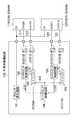
同図では、半導体集積回路100及び2つのDDR−SDRAM110、120によってメモリシステムが構成される。前記半導体集積回路100は、クロック発生回路101によって生成されたクロックに同期して動作する2つのDDR−SDRAM110、120からのリードデータDQ[7:0]、DQ[15:8]を取り込んで転送する。DDR−SDRAM110、120は、互いに同一のクロック系統に接続されている。このクロック系統は、クロック発生回路101によって発生されるクロックの系統である。 In the drawing, a semiconductor integrated circuit 100 and two DDR-
前記半導体集積回路100は、その内部に、ラッチタイミング制御回路102、103、リードバッファ104、105、およびリードタイミング制御回路106を備える。 The semiconductor integrated circuit 100 includes latch
また、前記半導体集積回路100は、DDR−SDRAM110からのデータストローブ信号DQS[0]を伝達するデータストローブ信号線111、およびDDR−SDRAM110からのリードデータDQ[7:0]を伝達するデータ信号線112によってDDR−SDRAM110と接続されている。また、前記半導体集積回路100は、DDR−SDRAM120からのデータストローブ信号DQS[1]を伝達するデータストローブ信号線121、およびDDR−SDRAM120からのリードデータDQ[15:8]を伝達するデータ信号線122によってDDR−SDRAM120と接続されている。 The semiconductor integrated circuit 100 also includes a data
リードバッファ104は、前記DDR−SDRAM110からのリードデータDQ[7:0]を取り込んで転送する。リードバッファ105は、前記DDR−SDRAM120からのリードデータDQ[15:8]を取り込んで転送する。 The
ラッチタイミング制御回路102は、1つのDDR−SDRAM110からのデータストローブ信号DQS[0]に基づいて、前記リードバッファ104が前記DDR−SDRAM110からのリードデータDQ[7:0]を取り込むラッチタイミングLTI1を制御する。リードバッファ104は、前記ラッチタイミング制御回路102のラッチタイミングLTI1に基づいて、前記DDR−SDRAM110からのリードデータDQ[7:0]を取り込む。 Based on the data strobe signal DQS [0] from one DDR-
また、ラッチタイミング制御回路103は、他の1つのDDR−SDRAM120からのデータストローブ信号DQS[1]に基づいて、前記リードバッファ105が前記DDR−SDRAM120からのリードデータDQ[15:8]を取り込むラッチタイミングLTI2を制御する。リードバッファ105は、前記ラッチタイミング制御回路103のラッチタイミングLTI2に基づいて、前記DDR−SDRAM120からのリードデータDQ[15:8]を取り込む。 The latch
リードタイミング制御回路106は、前記ラッチタイミング制御回路102、103からのラッチタイミングLTI1、LTI2に基づいて生成されるラッチ終了信号LES1、LES2によって、前記リードバッファ104、105がリードデータDI[7:0]、DI[15:8]を転送するリードタイミングRTIを制御する。つまり、リードタイミング制御回路106は、各リードバッファ104、105に対して、それぞれ、リードタイミングを制御する。ここで、前記リードデータDQ[7:0]と前記リードデータDI[7:0]とは同一のデータであり、前記リードデータDQ[15:8]と前記リードデータDI[15:8]とは同一のデータである。 The read
前記半導体集積回路100は、データストローブ信号DQS[0]、DQS[1]毎、すなわち本実施形態では、DDR−SDRAM110、120毎に、ラッチタイミング制御回路102、103とリードバッファ104、105とを備えている。つまり、半導体集積回路100は、データストローブ信号DQS[0]に対応して、ラッチタイミング制御回路102とリードバッファ104とを備え、データストローブ信号DQS[1]に対応して、ラッチタイミング制御回路103とリードバッファ105とを備えている。言い換えると、半導体集積回路100は、DDR−SDRAM110に対応して、ラッチタイミング制御回路102とリードバッファ104とを備え、DDR−SDRAM120に対応して、ラッチタイミング制御回路103とリードバッファ105とを備えている。 The semiconductor integrated circuit 100 includes latch
前記リードバッファ104、105は、前記リードタイミング制御回路106からのリードタイミングRTIに基づいて、リードデータDI[7:0]、DI[15:8]を転送する。 The read buffers 104 and 105 transfer read data DI [7: 0] and DI [15: 8] based on the read timing RTI from the read
前記リードタイミング制御回路106は、その内部にリードタイミング指示回路(図示せず)を有し、前記リードタイミング指示回路によって、当該半導体集積回路100に備えた全てのラッチタイミング制御回路102、103がラッチ終了信号LES1、LES2を出力したことを判定し、この判定の後に、当該半導体集積回路100に備えたリードバッファ104、105からリードデータDI[7:0]、DI[15:8]を転送させる。 The read
図2は、ラッチタイミング制御回路102の全体構成のブロック図である。 FIG. 2 is a block diagram of the overall configuration of the latch
同図において、ラッチタイミング制御回路102は、データストローブ信号DQS[0]のエッジ毎にラッチタイミングLTI1を指示するラッチタイミング指示回路201と、図1のリードバッファ104に取り込むリードデータDQ[7:0]のデータ数をカウントするラッチカウント回路202と、前記ラッチカウント回路202のカウント数と所定の基準値とを比較して、前記カウント数が前記所定の基準値に達したとき、ラッチ終了信号LES1を生成する比較回路203とを備える。前記比較回路の所定の基準値は、「1」値以上の固定値であり、例えば「2」値である。 In the figure, the latch
また、ラッチタイミング制御回路103の内部にも、上記のように、ラッチタイミング指示回路、ラッチカウント回路、及び比較回路が設けられる。 The latch
図3は、本実施形態の半導体集積回路100におけるラッチタイミングを示す模式図である。 FIG. 3 is a schematic diagram showing latch timing in the semiconductor integrated circuit 100 of the present embodiment.
同図に示すように、本実施形態のラッチタイミング制御回路102、103に設けられたラッチタイミング指示回路201は、各々に入力されるデータストローブ信号DQS[0]、DQS[1]のエッジ毎にラッチタイミングLTI1、LTI2を指示する。リードバッファ104は、前記ラッチタイミング制御回路102からのラッチタイミングLTI1に基づいて、リードデータDQ[7:0]を1バイト(A1、A2、A3、A4)毎に取り込み、リードバッファ105は、前記ラッチタイミング制御回路103からのラッチタイミングLTI2に基づいて、リードデータDQ[15:8]を1バイト(B1、B2、B3、B4)毎に取り込む。この際、各々のデータストローブ信号DQS[0]、DQS[1]のエッジ毎に前記ラッチタイミングLTI1、LTI2を指示するので、データストローブ信号DQS[0]、DQS[1]のエッジ毎にデータバッファの状態を監視して、各々のリードデータA1〜A4、B1〜B4の1バイトがすべてそろった時点でリードバッファ104、105に前記各々のリードデータA1〜A4、B1〜B4を取り込む。 As shown in the figure, the latch
以上のように、本実施形態では、半導体集積回路100の外部に遅延回路を設ける必要がないので、メモリシステムの基盤実装がより従来よりも単純になると共に、リードデータDQ[7:0]、DQ[15:8]をリードバッファ104、105に取り込んでラッチするラッチタイミングLT1、LT2を制御するので円滑にリードデータDQ[7:0]、DQ[15:8]を取り込むことが可能である。 As described above, in this embodiment, since it is not necessary to provide a delay circuit outside the semiconductor integrated circuit 100, the basic mounting of the memory system becomes simpler than before, and the read data DQ [7: 0], Since the latch timings LT1 and LT2 for fetching and latching DQ [15: 8] into the read buffers 104 and 105 are controlled, it is possible to smoothly fetch the read data DQ [7: 0] and DQ [15: 8]. .
また、ラッチタイミング指示回路201が、各DQSのエッジ毎にラッチタイミングを指示し、各々のリードデータA1〜A4、B1〜B4を構成する1バイトのデータがすべてそろった時点でリードバッファ104、105が取り込みを行うので、メモリアクセス速度の向上を実現することが可能となると共に、同一のクロック系統で複数のDDR−SDRAMを駆動することが可能となる。 Further, the latch
尚、図1では、2つのDDR−SDRAMを備えたメモリシステムを示したが、本実施形態のメモリシステムは、3個以上のDDR−SDRAMが半導体集積回路100に接続される構成によって実現されてもよい。その場合には、各DDR−SDRAMのデータストローブ信号のエッジ毎にリードデータのデータバッファの状態を監視して、リードバッファへの取り込みを開始することが可能である。 1 shows a memory system including two DDR-SDRAMs, the memory system according to the present embodiment is realized by a configuration in which three or more DDR-SDRAMs are connected to the semiconductor integrated circuit 100. Also good. In that case, it is possible to monitor the state of the data buffer of the read data for each edge of the data strobe signal of each DDR-SDRAM and start taking in the read buffer.
また、半導体集積回路100とDDR−SDRAM110、120間の配線については、データストローブ信号線のみを等長配線とすればよく、データ信号線等、その他の配線については、等長配線を考慮する必要がないので、実装における制約事項が減り、従来よりも容易に実装することが可能である。 In addition, as for the wiring between the semiconductor integrated circuit 100 and the DDR-
また、本実施形態において半導体集積回路100に接続されるDDR−SDRAMは1つであってもよい。 In the present embodiment, one DDR-SDRAM may be connected to the semiconductor integrated circuit 100.
さらに、前記比較回路203の所定の基準値を「2」値と設定したが、図1の半導体集積回路100の外部のCPU(図示せず)によって設定可能な構成にして、プログラムの実行時に遅延時間を調整してもよい。 Further, although the predetermined reference value of the
《実施形態2》
図4は、本発明の実施形態2のメモリシステムにおける要部構成のブロック図である。<<
FIG. 4 is a block diagram of a main configuration in the memory system according to the second embodiment of the present invention.
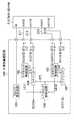
同図に示すように、本実施形態のメモリシステムは、2つのDDR−SDRAM110、120に代えて、1つのDDR−SDRAM210が接続される点において、実施形態1のメモリシステムと異なっている。また、DDR−SDRAM210は、複数のデータストローブ信号線を介して半導体集積回路100に接続される。 As shown in the figure, the memory system of the present embodiment is different from the memory system of the first embodiment in that one DDR-
DDR−SDRAM210は、2つのデータストローブ信号DQS[0]、DQS[1]を出力する。半導体集積回路100は、DDR−SDRAM210からのリードデータDQ[7:0]、DQ[15:8]を取り込んで転送する。リードデータDQ[7:0]、DQ[15:8]は、クロック発生回路101によって生成されたクロックに同期した信号である。 The DDR-
半導体集積回路100は、データストローブ信号DQS[0]を伝達するデータストローブ信号線211、データストローブ信号DQS[0]に対応するリードデータDQ[7:0]を伝達するデータ信号線212、データストローブ信号DQS[1]を伝達するデータストローブ信号線213、およびデータストローブ信号DQS[1]に対応するリードデータDQ[15:8]を伝達するデータ信号線214によって、DDR−SDRAM210と接続されている。 The semiconductor integrated circuit 100 includes a data
半導体集積回路100は、1つのDDR−SDRAM210からのデータストローブ信号DQS[0]、DQS[1]毎に、ラッチタイミング制御回路102、103とリードバッファ104、105とを備えている。つまり、半導体集積回路100は、データストローブ信号DQS[0]に対応して、ラッチタイミング制御回路102とリードバッファ104とを備え、データストローブ信号DQS[1]に対応して、ラッチタイミング制御回路103とリードバッファ105とを備えている。 The semiconductor integrated circuit 100 includes latch
尚、図4では、複数のデータストローブ信号を有するDDR−SDRAMを1つ備えたメモリシステムを示したが、本実施形態のメモリシステムは、複数のデータストローブ信号を有する複数のDDR−SDRAMが半導体集積回路100に接続される構成で実現されてもよい。その場合には、各DDR−SDRAMの各データストローブ信号のエッジ毎にリードデータのデータバッファの状態を監視して、リードバッファへの取り込みを開始することが可能である。 FIG. 4 shows a memory system including one DDR-SDRAM having a plurality of data strobe signals. However, in the memory system according to the present embodiment, a plurality of DDR-SDRAMs having a plurality of data strobe signals is a semiconductor. It may be realized by a configuration connected to the integrated circuit 100. In that case, it is possible to monitor the state of the data buffer of the read data for each edge of each data strobe signal of each DDR-SDRAM and start taking in the read buffer.
また、半導体集積回路100とDDR−SDRAM210間の配線については、データストローブ信号線のみを等長配線とすればよく、データ信号線等、その他の配線については、等長配線を考慮する必要がないので、実装における制約事項が減り、従来よりも容易に実装することが可能である。 In addition, as for the wiring between the semiconductor integrated circuit 100 and the DDR-
《実施形態3》
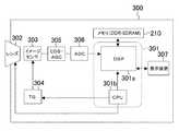
本発明の実施形態3の電子撮像装置300は、半導体集積回路301、クロックに同期して動作するDDR−SDRAM210、レンズ302、イメージセンサ303、TG(Timing Generator)304、CDS・AGC(Correlated Double Sampling、Automatic Gain Control)305、ADC(Analog to Digital Converter)306、および表示装置307を備えている。また、半導体集積回路301は、半導体集積回路100を含んでおり、DSP(Digital Signal Processor)301a、およびCPU(Central Processing Unit)301bを搭載している。<< Embodiment 3 >>
An
なお、電子撮像装置300が、DDR−SDRAM210に代えて、DDR−SDRAM110およびDDR−SDRAM120を備えるようにしてもよい。また、DDR−SDRAM110、120のように1つのデータストローブ信号を出力するDDR−SDRAMを3つ以上備えてもよいし、1つのデータストローブ信号を出力するDDR−SDRAMと2つ以上のデータストローブ信号を出力するDDR−SDRAMとを両方備えてもよい。 The
また、電子撮像装置300が、レンズ302、およびイメージセンサ303をそれぞれ複数備えるようにしてもよい。 Further, the
以上説明したように、本発明は、半導体集積回路の外部に遅延回路を設けることなく、DDR−SDRAMからの高速なリードデータの確実な取り込みを単純な構成で実現するので、特に、クロックに同期して動作するDDR−SDRAMからのリードデータを取り込んで転送する半導体集積回路等として有用である。 As described above, the present invention realizes high-speed read data reliably fetched from the DDR-SDRAM with a simple configuration without providing a delay circuit outside the semiconductor integrated circuit. It is useful as a semiconductor integrated circuit or the like that takes in and transfers read data from a DDR-SDRAM that operates as described above.
本発明は、ダブルデータレート方式のシンクロナスダイナミックランダムアクセスメモリ(DDR−SDRAM)が接続されるメモリコントローラを有する半導体集積回路に関するものである。 The present invention relates to a semiconductor integrated circuit having a memory controller to which a double data rate type synchronous dynamic random access memory (DDR-SDRAM) is connected.
現在、多くのメモリシステムでは、クロックに同期して動作するDRAM(Dynamic Random Access Memory)であるSDRAM(Synchronous DRAM)が用いられている。特に、近年では、高速なデータ転送機能を持ったSDRAMであるDDR−SDRAM(Double Data Rate SDRAM)が注目を集めている。DDR−SDRAMは、クロックの立ち上がりと立ち下がりの両エッジに同期してデータ転送を行うので、従来のSDRAMの2倍の高速データ転送が可能である。Currently, in many memory systems, an SDRAM (Synchronous DRAM) which is a DRAM (Dynamic Random Access Memory) that operates in synchronization with a clock is used. In particular, in recentyears, DDR-SDRAM (Double Dat a Rate SDRAM) has attracted attention as a SDRAM having a high-speed data transfer capabilities. Since the DDR-SDRAM performs data transfer in synchronization with both rising and falling edges of the clock, it can transfer data twice as fast as the conventional SDRAM.
DDR−SDRAMを備えたメモリシステム内のメモリコントローラは、1バイトのデータ毎に出力されるデータストローブ信号(DQS)のタイミングに基づいて、1バイト単位でDDR−SDRAMからリードデータを取り込む。例えば、32ビットのシステムバスを用いる場合には、1バイト単位で取り込んだリードデータを4つまとめて、メモリシステムの外部に出力する。 A memory controller in a memory system including a DDR-SDRAM fetches read data from the DDR-SDRAM in units of one byte based on the timing of a data strobe signal (DQS) output for each byte of data. For example, when a 32-bit system bus is used, four pieces of read data taken in 1-byte units are collected and output to the outside of the memory system.
DDR−SDRAMからリードデータを取り込む際には、DQSとリードデータとの位相を合わせて正常にリードデータをラッチするために、DQSがDDR−SDRAMからメモリコントローラに到達するまでの信号到達時間と、リードデータがDDR−SDRAMからメモリコントローラに到達するまでの信号到達時間とが同等となるように、データストローブ信号線とデータ信号線とを等長に配線してメモリコントローラとDDR−SDRAMとを接続する必要があった。 When fetching the read data from the DDR-SDRAM, in order to properly latch the read data in accordance with the phase of the DQS and the read data, a signal arrival time until the DQS reaches the memory controller from the DDR-SDRAM, Connect the memory controller and the DDR-SDRAM by arranging the data strobe signal line and the data signal line to have the same length so that the signal arrival time until the read data reaches the memory controller from the DDR-SDRAM becomes equal. There was a need to do.
従来、前記のような信号到達時間を同等にする技術として、例えば特許文献1に記載されるように、DDR−SDRAMと、そのDDR−SDRAMのコントロールを行う半導体集積回路との間に遅延回路を設けて、メモリシステムの外部に設けたCPUからのアクセスによって、クロックの遅延時間及びDQSの遅延時間を調整する技術が知られている。 Conventionally, as a technique for equalizing the signal arrival times as described above, for example, as described in
以下に、このような従来のメモリシステムにおける信号到達時間の調整に関する従来技術を説明する。 Hereinafter, a conventional technique relating to the adjustment of the signal arrival time in such a conventional memory system will be described.
図6は、従来のメモリシステムの要部構成のブロック図である。同図において、従来のメモリシステムは、DDR−SDRAMのコントロールを行う半導体集積回路1と、クロック発生回路2と、2つのDDR−SDRAM3、4と、信号を遅延させる遅延回路5、6、7、8とを備える。上記のメモリシステムでは、その外部に備えたCPUからのアクセスによって、DDR−SDRAM3、4に供給されるクロックの遅延時間及び、前記半導体集積回路1と前記DDR−SDRAM3、4との間を伝播するデータストローブ信号DQS[0]、DQS[1]の遅延時間を調整する。前記遅延回路6、8を用いて、データストローブ信号DQS[0]、DQS[1]とリードデータDQ[7:0]、DQ[15:8]との間の遅延時間を調整することで、前記DDR−SDRAM3、4から前記半導体集積回路1に供給されるデータストローブ信号DQS[0]、DQS[1]とリードデータDQ[7:0]、DQ[15:8]との位相を合わせて、円滑にリードデータDQ[7:0]、DQ[15:8]を取り込む。
しかしながら、前記従来のメモリシステムでは、半導体集積回路1の外部に遅延回路5〜8を設けるので、メモリシステムの設計が複雑になる。また、前記遅延回路5〜8における遅延時間を予め設定する必要があるので、当該メモリシステムの動作中の電圧変動や温度変化による遅延に対処するために遅延時間にマージンを持たせる必要がある。 However, in the conventional memory system, since the
本発明は、前記の課題に着目してなされたものであり、その目的はDDR−SDRAMからの高速なリードデータの取り込みが可能な半導体集積回路を単純な構成で実現することにある。 The present invention has been made paying attention to the above-described problems, and an object thereof is to realize a semiconductor integrated circuit capable of taking in high-speed read data from a DDR-SDRAM with a simple configuration.
本発明の第1の実施態様は、クロックに同期して動作するDDR−SDRAMからのリードデータを取り込んで転送する半導体集積回路であって、前記DDR−SDRAMからのリードデータを取り込んで転送するリードバッファと、前記DDR−SDRAMからのデータストローブ信号に基づいて、前記リードバッファが前記DDR−SDRAMからのリードデータを取り込むラッチタイミングを制御するラッチタイミング制御回路と、前記ラッチタイミング制御回路のラッチタイミングに基づいて、前記リードバッファがリードデータを転送するリードタイミングを制御するリードタイミング制御回路とを備えたことを特徴とする。 A first embodiment of the present invention is a semiconductor integrated circuit that takes in and transfers read data from a DDR-SDRAM that operates in synchronization with a clock, and that reads and transfers read data from the DDR-SDRAM. Based on a buffer, a data strobe signal from the DDR-SDRAM, a latch timing control circuit for controlling a latch timing at which the read buffer takes in read data from the DDR-SDRAM, and a latch timing of the latch timing control circuit. The read buffer includes a read timing control circuit for controlling a read timing for transferring read data.
これにより、DDR−SDRAMからのデータストローブ信号が半導体集積回路内のラッチタイミング制御回路に供給され、そのラッチタイミング制御回路によって、リードバッファがリードデータを取り込んでラッチするラッチタイミングが制御されるので、半導体集積回路の外部に遅延回路を設けることが不要となる。 Thereby, the data strobe signal from the DDR-SDRAM is supplied to the latch timing control circuit in the semiconductor integrated circuit, and the latch timing control circuit controls the latch timing at which the read buffer takes in and latches the read data. It is not necessary to provide a delay circuit outside the semiconductor integrated circuit.
また、ラッチタイミング制御回路がラッチタイミングを制御するので、半導体集積回路に、その動作中における電圧変動や温度変化による遅延に対処するための遅延時間のマージンを持たせることが不要となる。 In addition, since the latch timing control circuit controls the latch timing, it is not necessary for the semiconductor integrated circuit to have a delay time margin for coping with delay due to voltage fluctuation or temperature change during the operation.
本発明によれば、半導体集積回路の外部に遅延回路を設ける必要がないので、メモリシステムの基盤実装がより従来よりも単純になると共に、リードデータをリードバッファに取り込んでラッチするラッチタイミングが制御されるので、半導体集積回路の動作中に電圧変動や温度変化が発生した場合であっても円滑に且つ誤りなく確実にリードデータを取り込むことが可能である。 According to the present invention, since there is no need to provide a delay circuit outside the semiconductor integrated circuit, the basic mounting of the memory system becomes simpler than before, and the latch timing for fetching and latching the read data into the read buffer is controlled. Therefore, even when a voltage variation or a temperature change occurs during the operation of the semiconductor integrated circuit, it is possible to capture read data smoothly and surely without error.
以下、本発明の実施形態の半導体集積回路及びメモリシステムを図面に基づいて説明する。なお、以下の各実施形態において、他の実施形態と同様の機能を有する構成要素については同一の符号を付して説明を省略する。 Hereinafter, a semiconductor integrated circuit and a memory system according to embodiments of the present invention will be described with reference to the drawings. In each of the following embodiments, components having functions similar to those of the other embodiments are denoted by the same reference numerals and description thereof is omitted.
《実施形態1》
図1は、本発明の実施形態1のメモリシステムにおける要部構成のブロック図である。
FIG. 1 is a block diagram of a main configuration of the memory system according to the first embodiment of the present invention.
同図では、半導体集積回路100及び2つのDDR−SDRAM110、120によってメモリシステムが構成される。前記半導体集積回路100は、クロック発生回路101によって生成されたクロックに同期して動作する2つのDDR−SDRAM110、120からのリードデータDQ[7:0]、DQ[15:8]を取り込んで転送する。DDR−SDRAM110、120は、互いに同一のクロック系統に接続されている。このクロック系統は、クロック発生回路101によって発生されるクロックの系統である。 In the drawing, a semiconductor integrated circuit 100 and two DDR-
前記半導体集積回路100は、その内部に、ラッチタイミング制御回路102、103、リードバッファ104、105、およびリードタイミング制御回路106を備える。 The semiconductor integrated circuit 100 includes latch
また、前記半導体集積回路100は、DDR−SDRAM110からのデータストローブ信号DQS[0]を伝達するデータストローブ信号線111、およびDDR−SDRAM110からのリードデータDQ[7:0]を伝達するデータ信号線112によってDDR−SDRAM110と接続されている。また、前記半導体集積回路100は、DDR−SDRAM120からのデータストローブ信号DQS[1]を伝達するデータストローブ信号線121、およびDDR−SDRAM120からのリードデータDQ[15:8]を伝達するデータ信号線122によってDDR−SDRAM120と接続されている。 The semiconductor integrated circuit 100 also includes a data
リードバッファ104は、前記DDR−SDRAM110からのリードデータDQ[7:0]を取り込んで転送する。リードバッファ105は、前記DDR−SDRAM120からのリードデータDQ[15:8]を取り込んで転送する。 The read
ラッチタイミング制御回路102は、1つのDDR−SDRAM110からのデータストローブ信号DQS[0]に基づいて、前記リードバッファ104が前記DDR−SDRAM110からのリードデータDQ[7:0]を取り込むラッチタイミングLTI1を制御する。リードバッファ104は、前記ラッチタイミング制御回路102のラッチタイミングLTI1に基づいて、前記DDR−SDRAM110からのリードデータDQ[7:0]を取り込む。 Based on the data strobe signal DQS [0] from one DDR-
また、ラッチタイミング制御回路103は、他の1つのDDR−SDRAM120からのデータストローブ信号DQS[1]に基づいて、前記リードバッファ105が前記DDR−SDRAM120からのリードデータDQ[15:8]を取り込むラッチタイミングLTI2を制御する。リードバッファ105は、前記ラッチタイミング制御回路103のラッチタイミングLTI2に基づいて、前記DDR−SDRAM120からのリードデータDQ[15:8]を取り込む。 The latch
リードタイミング制御回路106は、前記ラッチタイミング制御回路102、103からのラッチタイミングLTI1、LTI2に基づいて生成されるラッチ終了信号LES1、LES2によって、前記リードバッファ104、105がリードデータDI[7:0]、DI[15:8]を転送するリードタイミングRTIを制御する。つまり、リードタイミング制御回路106は、各リードバッファ104、105に対して、それぞれ、リードタイミングを制御する。ここで、前記リードデータDQ[7:0]と前記リードデータDI[7:0]とは同一のデータであり、前記リードデータDQ[15:8]と前記リードデータDI[15:8]とは同一のデータである。 The read
前記半導体集積回路100は、データストローブ信号DQS[0]、DQS[1]毎、すなわち本実施形態では、DDR−SDRAM110、120毎に、ラッチタイミング制御回路102、103とリードバッファ104、105とを備えている。つまり、半導体集積回路100は、データストローブ信号DQS[0]に対応して、ラッチタイミング制御回路102とリードバッファ104とを備え、データストローブ信号DQS[1]に対応して、ラッチタイミング制御回路103とリードバッファ105とを備えている。言い換えると、半導体集積回路100は、DDR−SDRAM110に対応して、ラッチタイミング制御回路102とリードバッファ104とを備え、DDR−SDRAM120に対応して、ラッチタイミング制御回路103とリードバッファ105とを備えている。 The semiconductor integrated circuit 100 includes latch
前記リードバッファ104、105は、前記リードタイミング制御回路106からのリードタイミングRTIに基づいて、リードデータDI[7:0]、DI[15:8]を転送する。 The read buffers 104 and 105 transfer read data DI [7: 0] and DI [15: 8] based on the read timing RTI from the read
前記リードタイミング制御回路106は、その内部にリードタイミング指示回路(図示せず)を有し、前記リードタイミング指示回路によって、当該半導体集積回路100に備えた全てのラッチタイミング制御回路102、103がラッチ終了信号LES1、LES2を出力したことを判定し、この判定の後に、当該半導体集積回路100に備えたリードバッファ104、105からリードデータDI[7:0]、DI[15:8]を転送させる。 The read
図2は、ラッチタイミング制御回路102の全体構成のブロック図である。 FIG. 2 is a block diagram of the overall configuration of the latch
同図において、ラッチタイミング制御回路102は、データストローブ信号DQS[0]のエッジ毎にラッチタイミングLTI1を指示するラッチタイミング指示回路201と、図1のリードバッファ104に取り込むリードデータDQ[7:0]のデータ数をカウントするラッチカウント回路202と、前記ラッチカウント回路202のカウント数と所定の基準値とを比較して、前記カウント数が前記所定の基準値に達したとき、ラッチ終了信号LES1を生成する比較回路203とを備える。前記比較回路の所定の基準値は、「1」値以上の固定値であり、例えば「2」値である。 In the figure, the latch
また、ラッチタイミング制御回路103の内部にも、上記のように、ラッチタイミング指示回路、ラッチカウント回路、及び比較回路が設けられる。 The latch
図3は、本実施形態の半導体集積回路100におけるラッチタイミングを示す模式図である。 FIG. 3 is a schematic diagram showing latch timing in the semiconductor integrated circuit 100 of the present embodiment.
同図に示すように、本実施形態のラッチタイミング制御回路102、103に設けられたラッチタイミング指示回路201は、各々に入力されるデータストローブ信号DQS[0]、DQS[1]のエッジ毎にラッチタイミングLTI1、LTI2を指示する。リードバッファ104は、前記ラッチタイミング制御回路102からのラッチタイミングLTI1に基づいて、リードデータDQ[7:0]を1バイト(A1、A2、A3、A4)毎に取り込み、リードバッファ105は、前記ラッチタイミング制御回路103からのラッチタイミングLTI2に基づいて、リードデータDQ[15:8]を1バイト(B1、B2、B3、B4)毎に取り込む。この際、各々のデータストローブ信号DQS[0]、DQS[1]のエッジ毎に前記ラッチタイミングLTI1、LTI2を指示するので、データストローブ信号DQS[0]、DQS[1]のエッジ毎にデータバッファの状態を監視して、各々のリードデータA1〜A4、B1〜B4の1バイトがすべてそろった時点でリードバッファ104、105に前記各々のリードデータA1〜A4、B1〜B4を取り込む。 As shown in the figure, the latch
以上のように、本実施形態では、半導体集積回路100の外部に遅延回路を設ける必要がないので、メモリシステムの基盤実装がより従来よりも単純になると共に、リードデータDQ[7:0]、DQ[15:8]をリードバッファ104、105に取り込んでラッチするラッチタイミングLT1、LT2を制御するので円滑にリードデータDQ[7:0]、DQ[15:8]を取り込むことが可能である。 As described above, in this embodiment, since it is not necessary to provide a delay circuit outside the semiconductor integrated circuit 100, the basic mounting of the memory system becomes simpler than before, and the read data DQ [7: 0], Since the latch timings LT1 and LT2 for fetching and latching DQ [15: 8] into the read buffers 104 and 105 are controlled, it is possible to smoothly fetch the read data DQ [7: 0] and DQ [15: 8]. .
また、ラッチタイミング指示回路201が、各DQSのエッジ毎にラッチタイミングを指示し、各々のリードデータA1〜A4、B1〜B4を構成する1バイトのデータがすべてそろった時点でリードバッファ104、105が取り込みを行うので、メモリアクセス速度の向上を実現することが可能となると共に、同一のクロック系統で複数のDDR−SDRAMを駆動することが可能となる。 Further, the latch
尚、図1では、2つのDDR−SDRAMを備えたメモリシステムを示したが、本実施形態のメモリシステムは、3個以上のDDR−SDRAMが半導体集積回路100に接続される構成によって実現されてもよい。その場合には、各DDR−SDRAMのデータストローブ信号のエッジ毎にリードデータのデータバッファの状態を監視して、リードバッファへの取り込みを開始することが可能である。 1 shows a memory system including two DDR-SDRAMs, the memory system according to the present embodiment is realized by a configuration in which three or more DDR-SDRAMs are connected to the semiconductor integrated circuit 100. Also good. In that case, it is possible to monitor the state of the data buffer of the read data for each edge of the data strobe signal of each DDR-SDRAM and start taking in the read buffer.
また、半導体集積回路100とDDR−SDRAM110、120間の配線については、データストローブ信号線のみを等長配線とすればよく、データ信号線等、その他の配線については、等長配線を考慮する必要がないので、実装における制約事項が減り、従来よりも容易に実装することが可能である。 In addition, as for the wiring between the semiconductor integrated circuit 100 and the DDR-
また、本実施形態において半導体集積回路100に接続されるDDR−SDRAMは1つであってもよい。 In the present embodiment, one DDR-SDRAM may be connected to the semiconductor integrated circuit 100.
さらに、前記比較回路203の所定の基準値を「2」値と設定したが、図1の半導体集積回路100の外部のCPU(図示せず)によって設定可能な構成にして、プログラムの実行時に遅延時間を調整してもよい。 Further, although the predetermined reference value of the
《実施形態2》
図4は、本発明の実施形態2のメモリシステムにおける要部構成のブロック図である。<<
FIG. 4 is a block diagram of a main configuration in the memory system according to the second embodiment of the present invention.
同図に示すように、本実施形態のメモリシステムは、2つのDDR−SDRAM110、120に代えて、1つのDDR−SDRAM210が接続される点において、実施形態1のメモリシステムと異なっている。また、DDR−SDRAM210は、複数のデータストローブ信号線を介して半導体集積回路100に接続される。 As shown in the figure, the memory system of the present embodiment is different from the memory system of the first embodiment in that one DDR-
DDR−SDRAM210は、2つのデータストローブ信号DQS[0]、DQS[1]を出力する。半導体集積回路100は、DDR−SDRAM210からのリードデータDQ[7:0]、DQ[15:8]を取り込んで転送する。リードデータDQ[7:0]、DQ[15:8]は、クロック発生回路101によって生成されたクロックに同期した信号である。 The DDR-
半導体集積回路100は、データストローブ信号DQS[0]を伝達するデータストローブ信号線211、データストローブ信号DQS[0]に対応するリードデータDQ[7:0]を伝達するデータ信号線212、データストローブ信号DQS[1]を伝達するデータストローブ信号線213、およびデータストローブ信号DQS[1]に対応するリードデータDQ[15:8]を伝達するデータ信号線214によって、DDR−SDRAM210と接続されている。 The semiconductor integrated circuit 100 includes a data
半導体集積回路100は、1つのDDR−SDRAM210からのデータストローブ信号DQS[0]、DQS[1]毎に、ラッチタイミング制御回路102、103とリードバッファ104、105とを備えている。つまり、半導体集積回路100は、データストローブ信号DQS[0]に対応して、ラッチタイミング制御回路102とリードバッファ104とを備え、データストローブ信号DQS[1]に対応して、ラッチタイミング制御回路103とリードバッファ105とを備えている。 The semiconductor integrated circuit 100 includes latch
尚、図4では、複数のデータストローブ信号を有するDDR−SDRAMを1つ備えたメモリシステムを示したが、本実施形態のメモリシステムは、複数のデータストローブ信号を有する複数のDDR−SDRAMが半導体集積回路100に接続される構成で実現されてもよい。その場合には、各DDR−SDRAMの各データストローブ信号のエッジ毎にリードデータのデータバッファの状態を監視して、リードバッファへの取り込みを開始することが可能である。 FIG. 4 shows a memory system including one DDR-SDRAM having a plurality of data strobe signals. However, in the memory system according to the present embodiment, a plurality of DDR-SDRAMs having a plurality of data strobe signals is a semiconductor. It may be realized by a configuration connected to the integrated circuit 100. In that case, it is possible to monitor the state of the data buffer of the read data for each edge of each data strobe signal of each DDR-SDRAM and start taking in the read buffer.
また、半導体集積回路100とDDR−SDRAM210間の配線については、データストローブ信号線のみを等長配線とすればよく、データ信号線等、その他の配線については、等長配線を考慮する必要がないので、実装における制約事項が減り、従来よりも容易に実装することが可能である。 In addition, as for the wiring between the semiconductor integrated circuit 100 and the DDR-
《実施形態3》
本発明の実施形態3の電子撮像装置300は、半導体集積回路301、クロックに同期して動作するDDR−SDRAM210、レンズ302、イメージセンサ303、TG(Timing Generator)304、CDS・AGC(Correlated Double Sampling、Automatic Gain Control)305、ADC(Analog to Digital Converter)306、および表示装置307を備えている。また、半導体集積回路301は、半導体集積回路100を含んでおり、DSP(Digital Signal Processor)301a、およびCPU(Central Processing Unit)301bを搭載している。<< Embodiment 3 >>
An
なお、電子撮像装置300が、DDR−SDRAM210に代えて、DDR−SDRAM110およびDDR−SDRAM120を備えるようにしてもよい。また、DDR−SDRAM110、120のように1つのデータストローブ信号を出力するDDR−SDRAMを3つ以上備えてもよいし、1つのデータストローブ信号を出力するDDR−SDRAMと2つ以上のデータストローブ信号を出力するDDR−SDRAMとを両方備えてもよい。 The
また、電子撮像装置300が、レンズ302、およびイメージセンサ303をそれぞれ複数備えるようにしてもよい。 Further, the
以上説明したように、本発明は、半導体集積回路の外部に遅延回路を設けることなく、DDR−SDRAMからの高速なリードデータの確実な取り込みを単純な構成で実現するので、特に、クロックに同期して動作するDDR−SDRAMからのリードデータを取り込んで転送する半導体集積回路等として有用である。 As described above, the present invention realizes high-speed read data reliably fetched from the DDR-SDRAM with a simple configuration without providing a delay circuit outside the semiconductor integrated circuit. It is useful as a semiconductor integrated circuit or the like that takes in and transfers read data from a DDR-SDRAM that operates as described above.
100 半導体集積回路
101 クロック発生回路
102、103 ラッチタイミング制御回路
104、105 リードバッファ
106 リードタイミング制御回路
110、120、210 DDR−SDRAM
111、121 データストローブ信号線
112、122 データ信号線
201 ラッチタイミング指示回路
202 ラッチカウント回路
203 比較回路
211、213 データストローブ信号線
212、214 データ信号線
300 電子撮像装置
301 半導体集積回路
302 レンズ
303 イメージセンサ
304 TG
305 CDS・AGC
306 ADC
307 表示装置DESCRIPTION OF SYMBOLS 100 Semiconductor integrated
111, 121 Data
305 CDS / AGC
306 ADC
307 display device
Claims (11)
Translated fromJapanese前記DDR−SDRAMからのリードデータを取り込んで転送するリードバッファと、
前記DDR−SDRAMからのデータストローブ信号に基づいて、前記リードバッファが前記DDR−SDRAMからのリードデータを取り込むラッチタイミングを制御するラッチタイミング制御回路と、
前記ラッチタイミング制御回路のラッチタイミングに基づいて、前記リードバッファがリードデータを転送するリードタイミングを制御するリードタイミング制御回路とを備えた
ことを特徴とする半導体集積回路。A semiconductor integrated circuit that takes in and transfers read data from a DDR-SDRAM that operates in synchronization with a clock,
A read buffer for fetching and transferring read data from the DDR-SDRAM;
A latch timing control circuit for controlling a latch timing at which the read buffer takes in read data from the DDR-SDRAM based on a data strobe signal from the DDR-SDRAM;
A semiconductor integrated circuit comprising: a read timing control circuit that controls a read timing at which the read buffer transfers read data based on a latch timing of the latch timing control circuit.
複数の前記DDR−SDRAMからのリードデータを取り込んで転送するものであり、
前記ラッチタイミング制御回路および前記リードバッファを、前記複数のDDR−SDRAMからのデータストローブ信号毎に備え、
前記リードタイミング制御回路は、前記各リードバッファに対して、それぞれ、リードタイミングの制御を行う
ことを特徴とする半導体集積回路。The semiconductor integrated circuit according to claim 1,
Read and transfer read data from a plurality of the DDR-SDRAMs,
The latch timing control circuit and the read buffer are provided for each data strobe signal from the plurality of DDR-SDRAMs,
The semiconductor integrated circuit according to claim 1, wherein the read timing control circuit controls read timing for each of the read buffers.
複数の前記DDR−SDRAMからのリードデータを取り込んで転送するものであり、
前記ラッチタイミング制御回路および前記リードバッファを、前記DDR−SDRAM毎に備え、
前記リードタイミング制御回路は、前記各リードバッファに対して、それぞれ、リードタイミングの制御を行う
ことを特徴とする半導体集積回路。The semiconductor integrated circuit according to claim 1,
Read and transfer read data from a plurality of the DDR-SDRAMs,
The latch timing control circuit and the read buffer are provided for each DDR-SDRAM,
The semiconductor integrated circuit according to claim 1, wherein the read timing control circuit controls read timing for each of the read buffers.
同一のクロック系統に接続された前記複数のDDR−SDRAMからのリードデータを取り込んで転送するものであり、
前記各DDR−SDRAMと、当該DDR−SDRAMからのデータストローブ信号を伝達するデータストローブ信号線、および当該DDR−SDRAMからのリードデータを伝達するデータ信号線によって接続されていることを特徴とする半導体集積回路。In the semiconductor integrated circuit of claim 3,
Read and transfer read data from the plurality of DDR-SDRAMs connected to the same clock system,
Each of the DDR-SDRAMs is connected to a data strobe signal line for transmitting a data strobe signal from the DDR-SDRAM and a data signal line for transmitting read data from the DDR-SDRAM. Integrated circuit.
複数のデータストローブ信号を出力する前記DDR−SDRAMからのリードデータを取り込んで転送するものであり、
前記DDR−SDRAMと、前記各データストローブ信号を伝達するデータストローブ信号線、および各データストローブ信号に対応するリードデータを伝達するデータ信号線によって接続されていることを特徴とする半導体集積回路。In the semiconductor integrated circuit of claim 1,
Read and transfer read data from the DDR-SDRAM that outputs a plurality of data strobe signals;
A semiconductor integrated circuit, wherein the DDR-SDRAM is connected to the data strobe signal line for transmitting each data strobe signal and the data signal line for transmitting read data corresponding to each data strobe signal.
前記ラッチタイミング制御回路は、
データストローブ信号のエッジ毎に前記ラッチタイミングを指示するラッチタイミング指示回路と、
前記リードバッファに取り込むリードデータのデータ数をカウントするラッチカウント回路と、
前記ラッチカウント回路のカウント数と所定の基準値とを比較して、前記カウント数が前記所定の基準値に達したとき、ラッチ終了信号を生成する比較回路とを備えた
ことを特徴とする半導体集積回路。The semiconductor integrated circuit according to claim 1,
The latch timing control circuit includes:
A latch timing instruction circuit for instructing the latch timing for each edge of the data strobe signal;
A latch count circuit that counts the number of read data to be taken into the read buffer;
A comparison circuit that compares a count number of the latch count circuit with a predetermined reference value, and generates a latch end signal when the count number reaches the predetermined reference value. Integrated circuit.
前記所定の基準値は、当該半導体集積回路の外部のCPUによって設定される
ことを特徴とする半導体集積回路。The semiconductor integrated circuit according to claim 6, wherein
The predetermined reference value is set by a CPU external to the semiconductor integrated circuit.
前記所定の基準値は、1以上の固定値である
ことを特徴とする半導体集積回路。The semiconductor integrated circuit according to claim 6, wherein
The predetermined reference value is a fixed value of 1 or more. A semiconductor integrated circuit, wherein:
前記リードタイミング制御回路は、
当該半導体集積回路に備えた全てのラッチタイミング制御回路がラッチ終了信号を出力したことを判定し、この判定の後、当該半導体集積回路に備えたリードバッファからリードデータを転送させる
ことを特徴とする半導体集積回路。The semiconductor integrated circuit according to claim 6, wherein
The read timing control circuit includes:
It is determined that all latch timing control circuits provided in the semiconductor integrated circuit output a latch end signal, and after this determination, read data is transferred from a read buffer provided in the semiconductor integrated circuit. Semiconductor integrated circuit.
クロックに同期して動作する少なくとも1つのDDR−SDRAMとを備えた
ことを特徴とするメモリシステム。A semiconductor integrated circuit according to claim 1;
A memory system comprising: at least one DDR-SDRAM that operates in synchronization with a clock.
クロックに同期して動作する少なくとも1つ以上のDDR−SDRAMと、
少なくとも1つ以上のレンズと、
少なくとも1つ以上のイメージセンサとを備えた
ことを特徴とする電子撮像装置。A semiconductor integrated circuit according to claim 1;
At least one DDR-SDRAM operating in synchronization with a clock;
At least one lens;
An electronic imaging apparatus comprising: at least one image sensor.
Applications Claiming Priority (3)
| Application Number | Priority Date | Filing Date | Title |
|---|---|---|---|
| JP2006227482 | 2006-08-24 | ||
| JP2006227482 | 2006-08-24 | ||
| PCT/JP2007/066452WO2008023793A1 (en) | 2006-08-24 | 2007-08-24 | Semiconductor integrated circuit, memory system and electronic imaging device |
Publications (1)
| Publication Number | Publication Date |
|---|---|
| JPWO2008023793A1true JPWO2008023793A1 (en) | 2010-01-14 |
Family
ID=39106874
Family Applications (1)
| Application Number | Title | Priority Date | Filing Date |
|---|---|---|---|
| JP2008530967APendingJPWO2008023793A1 (en) | 2006-08-24 | 2007-08-24 | Semiconductor integrated circuit, memory system, and electronic imaging device |
Country Status (3)
| Country | Link |
|---|---|
| US (1) | US7907472B2 (en) |
| JP (1) | JPWO2008023793A1 (en) |
| WO (1) | WO2008023793A1 (en) |
Families Citing this family (2)
| Publication number | Priority date | Publication date | Assignee | Title |
|---|---|---|---|---|
| US20230035693A1 (en)* | 2021-07-27 | 2023-02-02 | Synopsys, Inc. | Clock signal realignment for emulation of a circuit design |
| CN114649021B (en)* | 2022-03-14 | 2024-09-13 | 长鑫存储技术有限公司 | Margin adjustment method, margin adjustment circuit and memory |
Citations (7)
| Publication number | Priority date | Publication date | Assignee | Title |
|---|---|---|---|---|
| JPH08221315A (en)* | 1995-02-15 | 1996-08-30 | Hitachi Ltd | Information processing device |
| JPH1125029A (en)* | 1997-07-04 | 1999-01-29 | Fujitsu Ltd | Memory subsystem |
| JP2000207349A (en)* | 1999-01-13 | 2000-07-28 | Fujitsu Ltd | Memory access device |
| JP2004185608A (en)* | 2002-11-21 | 2004-07-02 | Matsushita Electric Ind Co Ltd | Data latch timing adjustment device |
| JP2006048226A (en)* | 2004-08-02 | 2006-02-16 | Fuji Photo Film Co Ltd | Semiconductor integrated circuit and photographing device |
| JP2006065470A (en)* | 2004-08-25 | 2006-03-09 | Fuji Xerox Co Ltd | Memory control method and device |
| JP2006189916A (en)* | 2004-12-28 | 2006-07-20 | Matsushita Electric Ind Co Ltd | Timing adjustment method and apparatus |
Family Cites Families (11)
| Publication number | Priority date | Publication date | Assignee | Title |
|---|---|---|---|---|
| US7044589B2 (en)* | 1997-07-12 | 2006-05-16 | Silverbrook Res Pty Ltd | Printing cartridge with barcode identification |
| US6529424B2 (en) | 2001-05-17 | 2003-03-04 | Koninklijke Philips Electronics N.V. | Propagation delay independent SDRAM data capture device and method |
| JP2003085974A (en) | 2001-09-13 | 2003-03-20 | Toshiba Corp | Semiconductor integrated circuit and memory system |
| JP4159415B2 (en)* | 2002-08-23 | 2008-10-01 | エルピーダメモリ株式会社 | Memory module and memory system |
| US6807125B2 (en)* | 2002-08-22 | 2004-10-19 | International Business Machines Corporation | Circuit and method for reading data transfers that are sent with a source synchronous clock signal |
| US6911851B2 (en) | 2002-11-21 | 2005-06-28 | Matsushita Electric Industrial Co., Ltd. | Data latch timing adjustment apparatus |
| US7089509B2 (en) | 2002-12-23 | 2006-08-08 | Sun Microsystems, Inc. | Controlling the propagation of a control signal by means of variable I/O delay compensation using a programmable delay circuit and detection sequence |
| US7184508B2 (en) | 2002-12-23 | 2007-02-27 | Sun Microsystems, Inc. | Capturing data and crossing clock domains in the absence of a free-running source clock |
| JP4450586B2 (en) | 2003-09-03 | 2010-04-14 | 株式会社ルネサステクノロジ | Semiconductor integrated circuit |
| US7532537B2 (en)* | 2004-03-05 | 2009-05-12 | Netlist, Inc. | Memory module with a circuit providing load isolation and memory domain translation |
| US7688672B2 (en)* | 2005-03-14 | 2010-03-30 | Rambus Inc. | Self-timed interface for strobe-based systems |
- 2007
- 2007-08-24JPJP2008530967Apatent/JPWO2008023793A1/enactivePending
- 2007-08-24WOPCT/JP2007/066452patent/WO2008023793A1/ennot_activeCeased
- 2007-08-24USUS12/302,450patent/US7907472B2/enactiveActive
Patent Citations (7)
| Publication number | Priority date | Publication date | Assignee | Title |
|---|---|---|---|---|
| JPH08221315A (en)* | 1995-02-15 | 1996-08-30 | Hitachi Ltd | Information processing device |
| JPH1125029A (en)* | 1997-07-04 | 1999-01-29 | Fujitsu Ltd | Memory subsystem |
| JP2000207349A (en)* | 1999-01-13 | 2000-07-28 | Fujitsu Ltd | Memory access device |
| JP2004185608A (en)* | 2002-11-21 | 2004-07-02 | Matsushita Electric Ind Co Ltd | Data latch timing adjustment device |
| JP2006048226A (en)* | 2004-08-02 | 2006-02-16 | Fuji Photo Film Co Ltd | Semiconductor integrated circuit and photographing device |
| JP2006065470A (en)* | 2004-08-25 | 2006-03-09 | Fuji Xerox Co Ltd | Memory control method and device |
| JP2006189916A (en)* | 2004-12-28 | 2006-07-20 | Matsushita Electric Ind Co Ltd | Timing adjustment method and apparatus |
Also Published As
| Publication number | Publication date |
|---|---|
| US7907472B2 (en) | 2011-03-15 |
| US20090154266A1 (en) | 2009-06-18 |
| WO2008023793A1 (en) | 2008-02-28 |
Similar Documents
| Publication | Publication Date | Title |
|---|---|---|
| JP5191555B2 (en) | Integrated circuit with bimodal data strobe | |
| JP4070051B2 (en) | Data masking method and circuit for semiconductor memory device, and semiconductor memory device having the circuit | |
| JP2010122842A (en) | Delay adjustment device, semiconductor device and delay adjustment method | |
| KR100942978B1 (en) | Semiconductor memory device | |
| JP2000276877A (en) | Synchronous semiconductor memory device having posted CAS latency function and CAS latency control method | |
| JP3832947B2 (en) | Data transfer memory device | |
| CN100442394C (en) | Semiconductor memory device and control method thereof | |
| JPWO2008023793A1 (en) | Semiconductor integrated circuit, memory system, and electronic imaging device | |
| JP2000100170A (en) | Integrated circuit device with input buffer that can support high-speed clock | |
| JP2003173290A (en) | Memory controller | |
| JP5113433B2 (en) | Memory controller | |
| JP3861650B2 (en) | Interface circuit | |
| CN1856835A (en) | Synchronous RAM memory circuit | |
| EP4127867B1 (en) | Improved clocking scheme to receive data | |
| US7080275B2 (en) | Method and apparatus using parasitic capacitance for synchronizing signals a device | |
| JP2000222877A (en) | Semiconductor memory | |
| JPH06295258A (en) | Semiconductor memory device and memory device | |
| JP2003116044A (en) | Data change method and electronic device using the same | |
| JP5072317B2 (en) | Memory controller | |
| JP2005070930A (en) | Memory control unit | |
| JPH1125030A (en) | Bus extension control circuit | |
| JPH11312116A (en) | Synchronizing device for synchronous dynamic random access memory | |
| JP2007241614A (en) | Skew adjustment circuit | |
| JP2009276914A (en) | Pseudo ddr memory interface circuit | |
| KR19980066738A (en) | Data input buffer of semiconductor memory device |
Legal Events
| Date | Code | Title | Description |
|---|---|---|---|
| A621 | Written request for application examination | Free format text:JAPANESE INTERMEDIATE CODE: A621 Effective date:20100202 | |
| RD02 | Notification of acceptance of power of attorney | Free format text:JAPANESE INTERMEDIATE CODE: A7422 Effective date:20120130 | |
| A131 | Notification of reasons for refusal | Free format text:JAPANESE INTERMEDIATE CODE: A131 Effective date:20120508 | |
| A02 | Decision of refusal | Free format text:JAPANESE INTERMEDIATE CODE: A02 Effective date:20120911 |