JPWO2007043697A1 - LIGHT EMITTING ELEMENT AND DISPLAY DEVICE - Google Patents
LIGHT EMITTING ELEMENT AND DISPLAY DEVICEDownload PDFInfo
- Publication number
- JPWO2007043697A1 JPWO2007043697A1JP2007540228AJP2007540228AJPWO2007043697A1JP WO2007043697 A1JPWO2007043697 A1JP WO2007043697A1JP 2007540228 AJP2007540228 AJP 2007540228AJP 2007540228 AJP2007540228 AJP 2007540228AJP WO2007043697 A1JPWO2007043697 A1JP WO2007043697A1
- Authority
- JP
- Japan
- Prior art keywords
- layer
- electrode
- carrier
- light emitting
- display device
- Prior art date
- Legal status (The legal status is an assumption and is not a legal conclusion. Google has not performed a legal analysis and makes no representation as to the accuracy of the status listed.)
- Pending
Links
- 238000002347injectionMethods0.000claimsabstractdescription90
- 239000007924injectionSubstances0.000claimsabstractdescription90
- 239000000463materialSubstances0.000claimsabstractdescription32
- 239000000758substrateSubstances0.000claimsabstractdescription14
- 239000004065semiconductorSubstances0.000claimsabstractdescription9
- 239000006185dispersionSubstances0.000claimsdescription47
- 239000010408filmSubstances0.000claimsdescription28
- 230000033228biological regulationEffects0.000claimsdescription19
- 239000011159matrix materialSubstances0.000claimsdescription14
- 229910052751metalInorganic materials0.000claimsdescription12
- 239000002184metalSubstances0.000claimsdescription12
- 229910044991metal oxideInorganic materials0.000claimsdescription8
- 150000004706metal oxidesChemical class0.000claimsdescription8
- 239000010409thin filmSubstances0.000claimsdescription5
- 230000001105regulatory effectEffects0.000claims1
- 239000010410layerSubstances0.000description214
- 230000015572biosynthetic processEffects0.000description18
- 238000000034methodMethods0.000description15
- 230000005525hole transportEffects0.000description14
- 238000001771vacuum depositionMethods0.000description11
- 238000000151depositionMethods0.000description9
- 230000008021depositionEffects0.000description9
- 239000003990capacitorSubstances0.000description7
- 229910052737goldInorganic materials0.000description7
- 239000010931goldSubstances0.000description7
- 229910052749magnesiumInorganic materials0.000description7
- 239000011777magnesiumSubstances0.000description7
- BASFCYQUMIYNBI-UHFFFAOYSA-NplatinumSubstances[Pt]BASFCYQUMIYNBI-UHFFFAOYSA-N0.000description7
- 229910052709silverInorganic materials0.000description7
- TVIVIEFSHFOWTE-UHFFFAOYSA-Ktri(quinolin-8-yloxy)alumaneChemical compound[Al+3].C1=CN=C2C([O-])=CC=CC2=C1.C1=CN=C2C([O-])=CC=CC2=C1.C1=CN=C2C([O-])=CC=CC2=C1TVIVIEFSHFOWTE-UHFFFAOYSA-K0.000description7
- 239000000969carrierSubstances0.000description5
- 230000004048modificationEffects0.000description5
- 238000012986modificationMethods0.000description5
- 229910052697platinumInorganic materials0.000description5
- VYPSYNLAJGMNEJ-UHFFFAOYSA-Nsilicon dioxideInorganic materialsO=[Si]=OVYPSYNLAJGMNEJ-UHFFFAOYSA-N0.000description5
- 238000004544sputter depositionMethods0.000description5
- 239000000126substanceSubstances0.000description5
- STTGYIUESPWXOW-UHFFFAOYSA-N2,9-dimethyl-4,7-diphenyl-1,10-phenanthrolineChemical compoundC=12C=CC3=C(C=4C=CC=CC=4)C=C(C)N=C3C2=NC(C)=CC=1C1=CC=CC=C1STTGYIUESPWXOW-UHFFFAOYSA-N0.000description4
- FYYHWMGAXLPEAU-UHFFFAOYSA-NMagnesiumChemical compound[Mg]FYYHWMGAXLPEAU-UHFFFAOYSA-N0.000description4
- 229910052782aluminiumInorganic materials0.000description4
- 150000001875compoundsChemical class0.000description4
- ZYGHJZDHTFUPRJ-UHFFFAOYSA-NcoumarinChemical compoundC1=CC=C2OC(=O)C=CC2=C1ZYGHJZDHTFUPRJ-UHFFFAOYSA-N0.000description4
- 239000002019doping agentSubstances0.000description4
- PCHJSUWPFVWCPO-UHFFFAOYSA-NgoldChemical compound[Au]PCHJSUWPFVWCPO-UHFFFAOYSA-N0.000description4
- 229910003437indium oxideInorganic materials0.000description4
- PJXISJQVUVHSOJ-UHFFFAOYSA-Nindium(iii) oxideChemical compound[O-2].[O-2].[O-2].[In+3].[In+3]PJXISJQVUVHSOJ-UHFFFAOYSA-N0.000description4
- 229920002120photoresistant polymerPolymers0.000description4
- 229920000642polymerPolymers0.000description4
- 230000008569processEffects0.000description4
- 239000004332silverSubstances0.000description4
- XOLBLPGZBRYERU-UHFFFAOYSA-Ntin dioxideChemical compoundO=[Sn]=OXOLBLPGZBRYERU-UHFFFAOYSA-N0.000description4
- IXHWGNYCZPISET-UHFFFAOYSA-N2-[4-(dicyanomethylidene)-2,3,5,6-tetrafluorocyclohexa-2,5-dien-1-ylidene]propanedinitrileChemical compoundFC1=C(F)C(=C(C#N)C#N)C(F)=C(F)C1=C(C#N)C#NIXHWGNYCZPISET-UHFFFAOYSA-N0.000description3
- 229910004298SiO 2Inorganic materials0.000description3
- 230000000903blocking effectEffects0.000description3
- 229910052792caesiumInorganic materials0.000description3
- TVFDJXOCXUVLDH-UHFFFAOYSA-Ncaesium atomChemical compound[Cs]TVFDJXOCXUVLDH-UHFFFAOYSA-N0.000description3
- XCJYREBRNVKWGJ-UHFFFAOYSA-Ncopper(II) phthalocyanineChemical compound[Cu+2].C12=CC=CC=C2C(N=C2[N-]C(C3=CC=CC=C32)=N2)=NC1=NC([C]1C=CC=CC1=1)=NC=1N=C1[C]3C=CC=CC3=C2[N-]1XCJYREBRNVKWGJ-UHFFFAOYSA-N0.000description3
- 239000011521glassSubstances0.000description3
- RBTKNAXYKSUFRK-UHFFFAOYSA-Nheliogen blueChemical compound[Cu].[N-]1C2=C(C=CC=C3)C3=C1N=C([N-]1)C3=CC=CC=C3C1=NC([N-]1)=C(C=CC=C3)C3=C1N=C([N-]1)C3=CC=CC=C3C1=N2RBTKNAXYKSUFRK-UHFFFAOYSA-N0.000description3
- 238000004519manufacturing processMethods0.000description3
- 229910052763palladiumInorganic materials0.000description3
- KDLHZDBZIXYQEI-UHFFFAOYSA-NpalladiumSubstances[Pd]KDLHZDBZIXYQEI-UHFFFAOYSA-N0.000description3
- 229920000767polyanilinePolymers0.000description3
- LLHKCFNBLRBOGN-UHFFFAOYSA-Npropylene glycol methyl ether acetateChemical compoundCOCC(C)OC(C)=OLLHKCFNBLRBOGN-UHFFFAOYSA-N0.000description3
- 239000010944silver (metal)Substances0.000description3
- 229920001665Poly-4-vinylphenolPolymers0.000description2
- GWEVSGVZZGPLCZ-UHFFFAOYSA-NTitan oxideChemical compoundO=[Ti]=OGWEVSGVZZGPLCZ-UHFFFAOYSA-N0.000description2
- RTAQQCXQSZGOHL-UHFFFAOYSA-NTitaniumChemical compound[Ti]RTAQQCXQSZGOHL-UHFFFAOYSA-N0.000description2
- VNSWULZVUKFJHK-UHFFFAOYSA-N[Sr].[Bi]Chemical compound[Sr].[Bi]VNSWULZVUKFJHK-UHFFFAOYSA-N0.000description2
- 150000001412aminesChemical class0.000description2
- 230000004888barrier functionEffects0.000description2
- 229910002115bismuth titanateInorganic materials0.000description2
- 229910052804chromiumInorganic materials0.000description2
- 230000000052comparative effectEffects0.000description2
- 229960000956coumarinDrugs0.000description2
- 235000001671coumarinNutrition0.000description2
- 238000010586diagramMethods0.000description2
- 229910052809inorganic oxideInorganic materials0.000description2
- 229910052741iridiumInorganic materials0.000description2
- IBHBKWKFFTZAHE-UHFFFAOYSA-Nn-[4-[4-(n-naphthalen-1-ylanilino)phenyl]phenyl]-n-phenylnaphthalen-1-amineChemical compoundC1=CC=CC=C1N(C=1C2=CC=CC=C2C=CC=1)C1=CC=C(C=2C=CC(=CC=2)N(C=2C=CC=CC=2)C=2C3=CC=CC=C3C=CC=2)C=C1IBHBKWKFFTZAHE-UHFFFAOYSA-N0.000description2
- 150000002894organic compoundsChemical class0.000description2
- TWNQGVIAIRXVLR-UHFFFAOYSA-Noxo(oxoalumanyloxy)alumaneChemical compoundO=[Al]O[Al]=OTWNQGVIAIRXVLR-UHFFFAOYSA-N0.000description2
- BPUBBGLMJRNUCC-UHFFFAOYSA-Noxygen(2-);tantalum(5+)Chemical compound[O-2].[O-2].[O-2].[O-2].[O-2].[Ta+5].[Ta+5]BPUBBGLMJRNUCC-UHFFFAOYSA-N0.000description2
- SLIUAWYAILUBJU-UHFFFAOYSA-NpentaceneChemical compoundC1=CC=CC2=CC3=CC4=CC5=CC=CC=C5C=C4C=C3C=C21SLIUAWYAILUBJU-UHFFFAOYSA-N0.000description2
- 229920000301poly(3-hexylthiophene-2,5-diyl) polymerPolymers0.000description2
- 229910021420polycrystalline siliconInorganic materials0.000description2
- 239000002861polymer materialSubstances0.000description2
- 229920005591polysiliconPolymers0.000description2
- 229920000123polythiophenePolymers0.000description2
- 229920005989resinPolymers0.000description2
- 239000011347resinSubstances0.000description2
- 235000012239silicon dioxideNutrition0.000description2
- 229910052814silicon oxideInorganic materials0.000description2
- 239000000243solutionSubstances0.000description2
- 238000004528spin coatingMethods0.000description2
- 229910001936tantalum oxideInorganic materials0.000description2
- NLDYACGHTUPAQU-UHFFFAOYSA-NtetracyanoethyleneChemical groupN#CC(C#N)=C(C#N)C#NNLDYACGHTUPAQU-UHFFFAOYSA-N0.000description2
- 229910001887tin oxideInorganic materials0.000description2
- OGIDPMRJRNCKJF-UHFFFAOYSA-Ntitanium oxideInorganic materials[Ti]=OOGIDPMRJRNCKJF-UHFFFAOYSA-N0.000description2
- UWRZIZXBOLBCON-VOTSOKGWSA-N(e)-2-phenylethenamineChemical classN\C=C\C1=CC=CC=C1UWRZIZXBOLBCON-VOTSOKGWSA-N0.000description1
- MVWPVABZQQJTPL-UHFFFAOYSA-N2,3-diphenylcyclohexa-2,5-diene-1,4-dioneChemical classO=C1C=CC(=O)C(C=2C=CC=CC=2)=C1C1=CC=CC=C1MVWPVABZQQJTPL-UHFFFAOYSA-N0.000description1
- 1250000017312-cyanoethyl groupChemical group[H]C([H])(*)C([H])([H])C#N0.000description1
- 229920003026AcenePolymers0.000description1
- NLHHRLWOUZZQLW-UHFFFAOYSA-NAcrylonitrileChemical compoundC=CC#NNLHHRLWOUZZQLW-UHFFFAOYSA-N0.000description1
- XMWRBQBLMFGWIX-UHFFFAOYSA-NC60 fullereneChemical compoundC12=C3C(C4=C56)=C7C8=C5C5=C9C%10=C6C6=C4C1=C1C4=C6C6=C%10C%10=C9C9=C%11C5=C8C5=C8C7=C3C3=C7C2=C1C1=C2C4=C6C4=C%10C6=C9C9=C%11C5=C5C8=C3C3=C7C1=C1C2=C4C6=C2C9=C5C3=C12XMWRBQBLMFGWIX-UHFFFAOYSA-N0.000description1
- OKTJSMMVPCPJKN-UHFFFAOYSA-NCarbonChemical compound[C]OKTJSMMVPCPJKN-UHFFFAOYSA-N0.000description1
- 241000284156Clerodendrum quadriloculareSpecies0.000description1
- 229920000742CottonPolymers0.000description1
- 229920001609Poly(3,4-ethylenedioxythiophene)Polymers0.000description1
- 239000004952PolyamideSubstances0.000description1
- 239000004642PolyimideSubstances0.000description1
- 239000004793PolystyreneSubstances0.000description1
- 239000004372Polyvinyl alcoholSubstances0.000description1
- 229920001218PullulanPolymers0.000description1
- 239000004373PullulanSubstances0.000description1
- NRCMAYZCPIVABH-UHFFFAOYSA-NQuinacridoneChemical compoundN1C2=CC=CC=C2C(=O)C2=C1C=C1C(=O)C3=CC=CC=C3NC1=C2NRCMAYZCPIVABH-UHFFFAOYSA-N0.000description1
- 229910052581Si3N4Inorganic materials0.000description1
- HCHKCACWOHOZIP-UHFFFAOYSA-NZincChemical compound[Zn]HCHKCACWOHOZIP-UHFFFAOYSA-N0.000description1
- XLOMVQKBTHCTTD-UHFFFAOYSA-NZinc monoxideChemical compound[Zn]=OXLOMVQKBTHCTTD-UHFFFAOYSA-N0.000description1
- XHCLAFWTIXFWPH-UHFFFAOYSA-N[O-2].[O-2].[O-2].[O-2].[O-2].[V+5].[V+5]Chemical compound[O-2].[O-2].[O-2].[O-2].[O-2].[V+5].[V+5]XHCLAFWTIXFWPH-UHFFFAOYSA-N0.000description1
- 229910045601alloyInorganic materials0.000description1
- 239000000956alloySubstances0.000description1
- 229940027991antiseptic and disinfectant quinoline derivativeDrugs0.000description1
- 150000004982aromatic aminesChemical class0.000description1
- 125000003118aryl groupChemical group0.000description1
- 229910052454barium strontium titanateInorganic materials0.000description1
- JRPBQTZRNDNNOP-UHFFFAOYSA-Nbarium titanateChemical compound[Ba+2].[Ba+2].[O-][Ti]([O-])([O-])[O-]JRPBQTZRNDNNOP-UHFFFAOYSA-N0.000description1
- 229910002113barium titanateInorganic materials0.000description1
- 229910021523barium zirconateInorganic materials0.000description1
- DQBAOWPVHRWLJC-UHFFFAOYSA-Nbarium(2+);dioxido(oxo)zirconiumChemical compound[Ba+2].[O-][Zr]([O-])=ODQBAOWPVHRWLJC-UHFFFAOYSA-N0.000description1
- 230000005540biological transmissionEffects0.000description1
- 229910052797bismuthInorganic materials0.000description1
- JCXGWMGPZLAOME-UHFFFAOYSA-Nbismuth atomChemical compound[Bi]JCXGWMGPZLAOME-UHFFFAOYSA-N0.000description1
- 125000000609carbazolyl groupChemical classC1(=CC=CC=2C3=CC=CC=C3NC12)*0.000description1
- 229910052799carbonInorganic materials0.000description1
- 238000010538cationic polymerization reactionMethods0.000description1
- 229910052681coesiteInorganic materials0.000description1
- 229920001940conductive polymerPolymers0.000description1
- 229920001577copolymerPolymers0.000description1
- 229910052802copperInorganic materials0.000description1
- 239000010949copperSubstances0.000description1
- PMHQVHHXPFUNSP-UHFFFAOYSA-Mcopper(1+);methylsulfanylmethane;bromideChemical compoundBr[Cu].CSCPMHQVHHXPFUNSP-UHFFFAOYSA-M0.000description1
- 229910052906cristobaliteInorganic materials0.000description1
- 230000007423decreaseEffects0.000description1
- 230000003247decreasing effectEffects0.000description1
- 239000000975dyeSubstances0.000description1
- 230000000694effectsEffects0.000description1
- 229920001971elastomerPolymers0.000description1
- 239000000806elastomerSubstances0.000description1
- 230000005684electric fieldEffects0.000description1
- 238000005401electroluminescenceMethods0.000description1
- 238000010894electron beam technologyMethods0.000description1
- 230000005669field effectEffects0.000description1
- 239000011810insulating materialSubstances0.000description1
- GKOZUEZYRPOHIO-UHFFFAOYSA-Niridium atomChemical compound[Ir]GKOZUEZYRPOHIO-UHFFFAOYSA-N0.000description1
- 229910052746lanthanumInorganic materials0.000description1
- FZLIPJUXYLNCLC-UHFFFAOYSA-Nlanthanum atomChemical compound[La]FZLIPJUXYLNCLC-UHFFFAOYSA-N0.000description1
- 239000002346layers by functionSubstances0.000description1
- 229910052451lead zirconate titanateInorganic materials0.000description1
- HFGPZNIAWCZYJU-UHFFFAOYSA-Nlead zirconate titanateChemical compound[O-2].[O-2].[O-2].[O-2].[O-2].[Ti+4].[Zr+4].[Pb+2]HFGPZNIAWCZYJU-UHFFFAOYSA-N0.000description1
- 229910052744lithiumInorganic materials0.000description1
- COQAIRYMVBNUKQ-UHFFFAOYSA-Jmagnesium;barium(2+);tetrafluorideChemical compound[F-].[F-].[F-].[F-].[Mg+2].[Ba+2]COQAIRYMVBNUKQ-UHFFFAOYSA-J0.000description1
- 150000002739metalsChemical class0.000description1
- 238000003801millingMethods0.000description1
- 239000000203mixtureSubstances0.000description1
- 229910052750molybdenumInorganic materials0.000description1
- DCZNSJVFOQPSRV-UHFFFAOYSA-Nn,n-diphenyl-4-[4-(n-phenylanilino)phenyl]anilineChemical classC1=CC=CC=C1N(C=1C=CC(=CC=1)C=1C=CC(=CC=1)N(C=1C=CC=CC=1)C=1C=CC=CC=1)C1=CC=CC=C1DCZNSJVFOQPSRV-UHFFFAOYSA-N0.000description1
- GKTNLYAAZKKMTQ-UHFFFAOYSA-Nn-[bis(dimethylamino)phosphinimyl]-n-methylmethanamineChemical classCN(C)P(=N)(N(C)C)N(C)CGKTNLYAAZKKMTQ-UHFFFAOYSA-N0.000description1
- 229910052759nickelInorganic materials0.000description1
- PXHVJJICTQNCMI-UHFFFAOYSA-NnickelSubstances[Ni]PXHVJJICTQNCMI-UHFFFAOYSA-N0.000description1
- 150000004767nitridesChemical class0.000description1
- -1nitro-substituted fluoreneChemical class0.000description1
- 229920003986novolacPolymers0.000description1
- 230000003287optical effectEffects0.000description1
- 125000002524organometallic groupChemical group0.000description1
- 150000004866oxadiazolesChemical class0.000description1
- RUDFQVOCFDJEEF-UHFFFAOYSA-Noxygen(2-);yttrium(3+)Chemical compound[O-2].[O-2].[O-2].[Y+3].[Y+3]RUDFQVOCFDJEEF-UHFFFAOYSA-N0.000description1
- 229960003540oxyquinolineDrugs0.000description1
- 125000002080perylenyl groupChemical classC1(=CC=C2C=CC=C3C4=CC=CC5=CC=CC(C1=C23)=C45)*0.000description1
- 239000005011phenolic resinSubstances0.000description1
- IEQIEDJGQAUEQZ-UHFFFAOYSA-NphthalocyanineChemical compoundN1C(N=C2C3=CC=CC=C3C(N=C3C4=CC=CC=C4C(=N4)N3)=N2)=C(C=CC=C2)C2=C1N=C1C2=CC=CC=C2C4=N1IEQIEDJGQAUEQZ-UHFFFAOYSA-N0.000description1
- 229920003023plasticPolymers0.000description1
- 239000004033plasticSubstances0.000description1
- 229920003227poly(N-vinyl carbazole)Polymers0.000description1
- 229920000058polyacrylatePolymers0.000description1
- 229920002647polyamidePolymers0.000description1
- 239000004417polycarbonateSubstances0.000description1
- 229920000515polycarbonatePolymers0.000description1
- 229920000728polyesterPolymers0.000description1
- 229920001721polyimidePolymers0.000description1
- 229920006254polymer filmPolymers0.000description1
- 229920002223polystyrenePolymers0.000description1
- 229920002451polyvinyl alcoholPolymers0.000description1
- 150000004033porphyrin derivativesChemical class0.000description1
- 235000019423pullulanNutrition0.000description1
- 150000003222pyridinesChemical class0.000description1
- 229940083082pyrimidine derivative acting on arteriolar smooth muscleDrugs0.000description1
- 150000003230pyrimidinesChemical class0.000description1
- 239000010453quartzSubstances0.000description1
- MCJGNVYPOGVAJF-UHFFFAOYSA-Nquinolin-8-olChemical compoundC1=CN=C2C(O)=CC=CC2=C1MCJGNVYPOGVAJF-UHFFFAOYSA-N0.000description1
- 150000003248quinolinesChemical class0.000description1
- 150000003252quinoxalinesChemical class0.000description1
- 238000010526radical polymerization reactionMethods0.000description1
- 230000006798recombinationEffects0.000description1
- 238000005215recombinationMethods0.000description1
- 230000009467reductionEffects0.000description1
- YYMBJDOZVAITBP-UHFFFAOYSA-NrubreneChemical compoundC1=CC=CC=C1C(C1=C(C=2C=CC=CC=2)C2=CC=CC=C2C(C=2C=CC=CC=2)=C11)=C(C=CC=C2)C2=C1C1=CC=CC=C1YYMBJDOZVAITBP-UHFFFAOYSA-N0.000description1
- 229910052710siliconInorganic materials0.000description1
- 239000010703siliconSubstances0.000description1
- 239000000377silicon dioxideSubstances0.000description1
- HQVNEWCFYHHQES-UHFFFAOYSA-Nsilicon nitrideChemical compoundN12[Si]34N5[Si]62N3[Si]51N64HQVNEWCFYHHQES-UHFFFAOYSA-N0.000description1
- 230000007480spreadingEffects0.000description1
- 238000003892spreadingMethods0.000description1
- 229910052682stishoviteInorganic materials0.000description1
- VEALVRVVWBQVSL-UHFFFAOYSA-Nstrontium titanateChemical compound[Sr+2].[O-][Ti]([O-])=OVEALVRVVWBQVSL-UHFFFAOYSA-N0.000description1
- 125000005504styryl groupChemical group0.000description1
- 230000001629suppressionEffects0.000description1
- 229910052715tantalumInorganic materials0.000description1
- 229920005992thermoplastic resinPolymers0.000description1
- 229920001187thermosetting polymerPolymers0.000description1
- 229910052719titaniumInorganic materials0.000description1
- 239000010936titaniumSubstances0.000description1
- 229910052905tridymiteInorganic materials0.000description1
- 125000006617triphenylamine groupChemical group0.000description1
- 229910052721tungstenInorganic materials0.000description1
- 229910001935vanadium oxideInorganic materials0.000description1
- 230000000007visual effectEffects0.000description1
- 229910052725zincInorganic materials0.000description1
- 239000011701zincSubstances0.000description1
Images


Classifications
- H—ELECTRICITY
- H10—SEMICONDUCTOR DEVICES; ELECTRIC SOLID-STATE DEVICES NOT OTHERWISE PROVIDED FOR
- H10K—ORGANIC ELECTRIC SOLID-STATE DEVICES
- H10K50/00—Organic light-emitting devices
- H10K50/10—OLEDs or polymer light-emitting diodes [PLED]
- H10K50/17—Carrier injection layers
- H—ELECTRICITY
- H10—SEMICONDUCTOR DEVICES; ELECTRIC SOLID-STATE DEVICES NOT OTHERWISE PROVIDED FOR
- H10K—ORGANIC ELECTRIC SOLID-STATE DEVICES
- H10K50/00—Organic light-emitting devices
- H—ELECTRICITY
- H10—SEMICONDUCTOR DEVICES; ELECTRIC SOLID-STATE DEVICES NOT OTHERWISE PROVIDED FOR
- H10K—ORGANIC ELECTRIC SOLID-STATE DEVICES
- H10K50/00—Organic light-emitting devices
- H10K50/10—OLEDs or polymer light-emitting diodes [PLED]
- H10K50/17—Carrier injection layers
- H10K50/171—Electron injection layers
- H—ELECTRICITY
- H10—SEMICONDUCTOR DEVICES; ELECTRIC SOLID-STATE DEVICES NOT OTHERWISE PROVIDED FOR
- H10K—ORGANIC ELECTRIC SOLID-STATE DEVICES
- H10K50/00—Organic light-emitting devices
- H10K50/30—Organic light-emitting transistors
- H—ELECTRICITY
- H10—SEMICONDUCTOR DEVICES; ELECTRIC SOLID-STATE DEVICES NOT OTHERWISE PROVIDED FOR
- H10K—ORGANIC ELECTRIC SOLID-STATE DEVICES
- H10K50/00—Organic light-emitting devices
- H10K50/80—Constructional details
- H10K50/805—Electrodes
- H—ELECTRICITY
- H10—SEMICONDUCTOR DEVICES; ELECTRIC SOLID-STATE DEVICES NOT OTHERWISE PROVIDED FOR
- H10K—ORGANIC ELECTRIC SOLID-STATE DEVICES
- H10K59/00—Integrated devices, or assemblies of multiple devices, comprising at least one organic light-emitting element covered by group H10K50/00
- H10K59/80—Constructional details
- H10K59/805—Electrodes
- H—ELECTRICITY
- H10—SEMICONDUCTOR DEVICES; ELECTRIC SOLID-STATE DEVICES NOT OTHERWISE PROVIDED FOR
- H10K—ORGANIC ELECTRIC SOLID-STATE DEVICES
- H10K50/00—Organic light-emitting devices
- H10K50/10—OLEDs or polymer light-emitting diodes [PLED]
- H10K50/18—Carrier blocking layers
- H—ELECTRICITY
- H10—SEMICONDUCTOR DEVICES; ELECTRIC SOLID-STATE DEVICES NOT OTHERWISE PROVIDED FOR
- H10K—ORGANIC ELECTRIC SOLID-STATE DEVICES
- H10K59/00—Integrated devices, or assemblies of multiple devices, comprising at least one organic light-emitting element covered by group H10K50/00
- H10K59/10—OLED displays
- H10K59/12—Active-matrix OLED [AMOLED] displays
- H10K59/125—Active-matrix OLED [AMOLED] displays including organic TFTs [OTFT]
Landscapes
- Physics & Mathematics (AREA)
- Optics & Photonics (AREA)
- Electroluminescent Light Sources (AREA)
- Devices For Indicating Variable Information By Combining Individual Elements (AREA)
Abstract
Translated fromJapaneseDescription
Translated fromJapanese本発明は、キャリア(正孔又は電子)分散性の有機薄膜を備えた発光素子およびその表示装置に関する。 The present invention relates to a light emitting element including a carrier (hole or electron) dispersible organic thin film and a display device thereof.
電界を印加して発光させる発光素子、例えば物質におけるキャリア(正孔又は電子)の再結合によるエレクトロルミネセンス(以下、単にELという)を利用している発光素子が知られている。例えば、有機化合物材料を用いた注入型の有機EL素子による表示パネルを搭載したEL表示装置が開発されている。有機EL素子には、赤色で発光する構造を有する赤色EL素子、緑色で発光する構造を有する緑色EL素子、及び青色で発光する構造を有する青色EL素子がある。これら赤、青、緑RGBで発光する3つの有機EL素子を1画素発光ユニットとして、複数画素をパネル部上にマトリクス状に配列すればカラー表示装置を実現することができる。かかるカラー表示装置による表示パネルの駆動方式として、パッシブマトリクス駆動型と、アクティブマトリクス駆動型が知られている。アクティブマトリクス駆動型のEL表示装置は、パッシブマトリクス型のものに比べて、低消費電力であり、また画素間のクロストークが少ないなどの利点を有し、特に大画面表示装置や高精細度表示装置に適している。
アクティブマトリクス駆動型のEL表示装置の表示パネルには、陽極電源ライン、陰極電源ライン、水平走査を担う走査ライン及び各走査ラインに交叉して配列されたデータラインが格子状に形成されている。走査ライン及びデータラインの各RGB交差部にRGBサブピクセルが形成されている。
サブピクセル毎に、走査ライン選択用の電界効果トランジスタ(FET:Field Effect Transistor)のゲートには走査ラインが接続され、そのドレインにはデータラインが接続されて、そのソースには発光駆動用のFETのゲートが接続されている。発光駆動FETのソースには陽極電源ラインを介して駆動電圧が印加され、そのドレインDにはEL素子の陽極端が接続されている。発光駆動FETのゲート及びソース間にはキャパシタが接続されている。更に、EL素子の陰極端には、陰極電源ラインを介して接地電位が印加される。
有機EL素子に代表される従来の有機発光素子は基本的にダイオード特性を示す能動素子であり、製品化されているものはほとんどパッシブマトリクス駆動によるものである。パッシブマトリクス駆動法では、線順次駆動を行うため瞬時的に高い輝度を必要とし、走査線数の限界数が限られてしまうため高精細な表示装置を得ることが難しかった。
ポリシリコンなどを用いたTFTを用いた有機EL表示装置が検討されているが、プロセス温度が高い、単位面積あたりの製造コストが高く大画面化に向かない、1画素内に2つ以上のトランジスタとコンデンサを配置しなければならないため開口率が下がり有機ELを高い輝度で発光させなければならないなどの欠点があった。
そこで基板上に、補助電極、絶縁層、陽極、発光層を含む有機機能層および陰極を順に配置して形成されており、陽極は、陰極に比べて面積が小となっている発光素子が提案されている(特開2002−343578公報参照)。かかる構成の発光素子においては、陽極と陰極との間に印加する電圧方向と同一の方向となるように、補助電極と陰極との間に電圧を印加することによって、陽極から発光層への正孔注入量が向上する。
かかる構成の発光素子は正孔注入を抑制することによって発光輝度を抑制する素子であるが、ON/OFF比が向上するように正孔注入層にはキャリア密度が少なく抵抗率の高い材料を用いている。かかる正孔注入層において、正孔は当該層の広がり方向には移動しにくく、結果として陽極と陰極とが最も近い部分において輝度が高く、陽極からの距離が離れるに従って輝度が減少することがわかった。すなわち、上記構成の発光素子において、正孔は、陽極の周縁において集中して注入されてしまい、発光素子が形成する画素内に発光ムラが生じるという問題があることが判った。また、正孔が集中して注入される領域は、発光層の劣化が早く、素子の寿命が短いという問題も判った。A light-emitting element that emits light by applying an electric field, for example, a light-emitting element that uses electroluminescence (hereinafter simply referred to as EL) due to recombination of carriers (holes or electrons) in a substance is known. For example, an EL display device equipped with a display panel using an injection type organic EL element using an organic compound material has been developed. The organic EL element includes a red EL element having a structure emitting red light, a green EL element having a structure emitting green light, and a blue EL element having a structure emitting blue light. A color display device can be realized by arranging these three organic EL elements that emit light of red, blue, and green RGB as a one-pixel light-emitting unit and arranging a plurality of pixels in a matrix on the panel portion. As a driving method of a display panel using such a color display device, a passive matrix driving type and an active matrix driving type are known. An active matrix driving type EL display device has advantages such as low power consumption and less crosstalk between pixels compared with a passive matrix type display device, and particularly, a large screen display device and a high definition display. Suitable for equipment.
In the display panel of an active matrix drive type EL display device, an anode power supply line, a cathode power supply line, a scanning line for performing horizontal scanning, and a data line arranged so as to cross each scanning line are formed in a grid pattern. An RGB subpixel is formed at each RGB intersection of the scanning line and the data line.
For each subpixel, a scanning line is connected to the gate of a field effect transistor (FET) for selecting a scanning line, a data line is connected to the drain, and a light emission driving FET is connected to the source. The gate is connected. A drive voltage is applied to the source of the light emission drive FET via the anode power supply line, and the anode end of the EL element is connected to the drain D thereof. A capacitor is connected between the gate and source of the light emission drive FET. Furthermore, a ground potential is applied to the cathode end of the EL element via a cathode power supply line.
Conventional organic light-emitting elements, typified by organic EL elements, are basically active elements that exhibit diode characteristics, and most products that are commercialized are driven by passive matrix driving. In the passive matrix driving method, line-sequential driving requires instantaneously high brightness, and the limit number of scanning lines is limited, so that it is difficult to obtain a high-definition display device.
Organic EL display devices using TFTs using polysilicon or the like are being studied, but two or more transistors in one pixel are not suitable for large screens due to high process temperature, high manufacturing cost per unit area Since the capacitor must be disposed, the aperture ratio is lowered and the organic EL must emit light with high luminance.
Therefore, an auxiliary electrode, an insulating layer, an anode, an organic functional layer including a light emitting layer, and a cathode are sequentially arranged on the substrate, and a light emitting device having a smaller area than the cathode is proposed for the anode. (See JP 2002-343578 A). In the light emitting device having such a configuration, a positive voltage from the anode to the light emitting layer is applied by applying a voltage between the auxiliary electrode and the cathode so as to be in the same direction as the voltage applied between the anode and the cathode. The amount of hole injection is improved.
The light-emitting element having such a structure is an element that suppresses light emission luminance by suppressing hole injection. However, a material with low carrier density and high resistivity is used for the hole injection layer so that the ON / OFF ratio is improved. ing. In such a hole injection layer, it is found that the holes do not easily move in the spreading direction of the layer, and as a result, the luminance is high at the portion where the anode and the cathode are closest, and the luminance decreases as the distance from the anode increases. It was. That is, it has been found that in the light emitting device having the above-described structure, holes are concentrated and injected at the periphery of the anode, and there is a problem that uneven light emission occurs in the pixel formed by the light emitting device. In addition, in the region where holes are concentrated and injected, the light emitting layer deteriorates quickly and the lifetime of the device is short.
本発明は、上記した問題が1例として挙げられる諸問題を解決する手段を提供することを目的とする。
請求項1記載の発光素子は、基板上に設けられている補助電極と、該補助電極上に設けられている絶縁層と、該絶縁層に支持されている第1電極と、該第1電極に接していてキャリア注入性の有機半導体材料からなるキャリア注入層と、該キャリア注入層に支持されている発光層と、該発光層に支持されている第2電極と、を含み、該キャリア注入層と該発光層との間に、該キャリア注入層よりも低抵抗のキャリア分散層を有する、ことを特徴とする。
請求項10記載の表示装置は、複数の発光部をマトリクス状に配置した表示装置であって、該発光部の各々は、基板上に設けられている補助電極と、該補助電極上に設けられている絶縁層と、該絶縁層に支持されている第1電極と、該第1電極に接していてキャリア注入性の有機半導体材料からなるキャリア注入層と、該キャリア注入層に支持されている発光層と、該発光層に支持されている第2電極と、を含み、該キャリア注入層と該発光層との間に、該キャリア注入層よりも低抵抗のキャリア分散層を有する、ことを特徴とする。An object of the present invention is to provide a means for solving various problems mentioned above as an example.
The light emitting device according to claim 1, wherein an auxiliary electrode provided on a substrate, an insulating layer provided on the auxiliary electrode, a first electrode supported by the insulating layer, and the first electrode A carrier injection layer made of an organic semiconductor material in contact with the carrier, a light emitting layer supported by the carrier injection layer, and a second electrode supported by the light emitting layer, the carrier injection A carrier dispersion layer having a lower resistance than the carrier injection layer is provided between the layer and the light emitting layer.
The display device according to
図1は本発明による有機EL素子の部分断面図である。
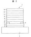
図2は本発明による有機EL素子の変形例の部分断面図である。
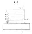
図3は本発明による有機EL素子の変形例の部分断面図である。
図4は本発明による有機EL素子の変形例の部分断面図である。
図5は本発明による有機EL素子の部分平面図である。
図6は本発明による有機EL素子のサブピクセル発光部を示す等価回路図である。
図7は本発明による有機EL素子の変形例の部分断面図である。
図8は本発明による有機EL素子の変形例の部分断面図である。FIG. 1 is a partial cross-sectional view of an organic EL device according to the present invention.
FIG. 2 is a partial sectional view of a modification of the organic EL element according to the present invention.
FIG. 3 is a partial sectional view of a modification of the organic EL device according to the present invention.
FIG. 4 is a partial sectional view of a modification of the organic EL element according to the present invention.
FIG. 5 is a partial plan view of an organic EL device according to the present invention.
FIG. 6 is an equivalent circuit diagram showing a sub-pixel light emitting portion of the organic EL device according to the present invention.
FIG. 7 is a partial cross-sectional view of a modification of the organic EL element according to the present invention.
FIG. 8 is a partial sectional view of a modification of the organic EL device according to the present invention.
以下、本発明による発光素子の一例として、有機EL素子について、添付図面を参照しつつ詳細に説明する。
図1に示す如く、有機EL素子1は、基板2上に設けられている補助電極3を含んでいる。基板2の材料としては、ガラス、石英、ポリスチレンなどのプラスチック材料といった半透明材料に限らず、シリコンやAlなどの不透明な材料、フェノール樹脂などの熱硬化性樹脂、ポリカーボネートなどの熱可塑性樹脂などを用いることができるがこれに限らない。
補助電極3上には絶縁層4が設けられている。絶縁層4は、SiO2、Si3N4に代表される種々の絶縁材料からなることができるものの、特に比誘電率の高い無機酸化物皮膜が好ましい。無機酸化物としては、酸化ケイ素、酸化アルミニウム、酸化タンタル、酸化チタン、酸化スズ、酸化バナジウム、チタン酸バリウムストロンチウム、ジルコニウム酸チタン酸バリウム、ジルコニウム酸チタン酸鉛、チタン酸鉛ランタン、チタン酸ストロンチウム、チタン酸バリウム、フッ化バリウムマグネシウム、チタン酸ビスマス、チタン酸ストロンチウムビスマス、タンタル酸ストロンチウムビスマス、タンタル酸ニオブ酸ビスマス、トリオキサイドイットリウムなどが挙げられる。それらのうち好ましいのは、酸化ケイ素、酸化アルミニウム、酸化タンタル、酸化チタンである。窒化ケイ素、窒化アルミニウムなどの無機窒化物も好適に用いることができる。また有機化合物皮膜としては、ポリイミド、ポリアミド、ポリエステル、ポリアクリレート、光ラジカル重合系、光カチオン重合系の光硬化性樹脂、あるいはアクリロニトリル成分を含有する共重合体、ポリビニルフェノール、ポリビニルアルコール、ノボラック樹脂、及びシアノエチルプルラン、ポリマー体、エラストマー体を含むホスファゼン化合物、などを用いることもできる。
絶縁層4上には陽極5が設けられており、かかる陽極5が第1電極となっている。陽極5は、後述する陰極10に比べて小なる面積を有している。すなわち、陽極5における陰極10と対向している面の面積は陰極10における陽極5と対向している面の面積よりも小となっている。また、陽極5は、櫛状、簾状又は格子状の形状に形成されていても良く、例えば図1に示すように、2本の櫛歯を有する櫛状体であることとしても良い。
陽極5は、キャリア注入性の有機半導体材料からなる正孔注入層6に接している。正孔注入層6は、陽極5からの正孔の注入を容易にする機能を有している。正孔注入層6に用いられる材料として、銅フタロシアニン(CuPc)に代表されるポルフィリン誘導体、ペタセンに代表されるポリアセン、m−TDATAに代表されるスターバーストアミンと呼ばれる高分子アリールアミンを使用することができる。また、ポリ(3−ヘキシルチオフェン)(P3HT)などの高分子材料を用いることができる。さらに、正孔注入層はこれらの材料の混合層若しくは積層したものでも良い。なお、正孔注入層は、真空蒸着法などの成膜方法を用いて形成することができる。
正孔注入層6は上方において、キャリア分散層7を支持している。キャリア分散層7は、正孔注入層6に比べて低抵抗であり、陽極5から注入されたキャリアを当該層が広がっている方向に拡散させる機能を有している。キャリア分散層7は、銅フタロシアニン(CuPc)や亜鉛フタロシアニン(ZnPc)、トリフェニルアミン誘導体などの有機半導体材料に、テトラシアノエチレン(TCNE)や四フッ化テトラシアノキノジメタン(F4−TCNQ)などのキャリア輸送材料(アクセプタ性分子)を混合して導電性を高くした層となっている。ここで、混合比率は重量比率でアクセプタ性分子が5〜50%の割合で混合されていることが好ましい。また、高分子系ではポリアニリン(PANI)、ポリチオフェン誘導体(PEDOT)などの高分子材料を用いることができる。
なお、添加される物質(ドーパント)の濃度は、キャリア分散層内において均一になっている場合に限定されず、キャリア分散層内で変化していることとしても良い。たとえば、キャリア分散層内におけるドーパントの濃度が正孔注入層から離れるに従って高くなることとしても良い。ドーパントの濃度を変化させることによって、キャリア分散層内におけるキャリアの拡散性が向上し、より均一にキャリアを発光層に注入することができる。
また、キャリア分散層7は、金属膜や金属酸化膜からなることとしても良い。金属膜に使用される材料として、Au,Pt,Pd,Ag,Al,Mgなどが選択できる。金属酸化膜としては、V2O5などの金属酸化物が使用できる。なお、金属膜および金属酸化膜の厚さは、当該薄膜を通過する光の透過効率を考慮して、100nm以下の厚さであることが好ましく、1nm〜30nm程度であることがより好ましい。
なお、キャリア分散層7は、補助電極3、陽極5、陰極(後述する)の何れの電極にも直接接する事がないように形成した方が好ましい。
また、キャリア分散層7は、第1電極となっている陽極5によって画定されるキャリア注入領域よりも大なる面積を有することが好ましい。ここでキャリア注入領域とは、陽極が櫛状、簾状又は格子状の形状に形成されている場合に発光素子において陽極に挟まれている領域をいう。例えば図1に示す如く陽極5が2本の櫛歯を有する櫛状体である場合、キャリア注入領域は、該櫛歯によって挟まれている領域となっている。
キャリア分散層7上には、正孔輸送層8が形成されている。正孔輸送層8は、キャリア分散層7からの正孔を安定に輸送する機能を有している。正孔輸送層8に使用される材料としては、トリフェニルジアミン誘導体、スチリルアミン誘導体、芳香族縮合環を有するアミン誘導体、カルバゾール誘導体、高分子材料としてはポリビニルカルバゾール及びその誘導体、ポリチオフェンなどが挙げられる。これらの化合物は2種以上を併用してもよい。さらに、一般的に、正孔輸送層8は正孔注入層6よりもイオン化ポテンシャルIpが大きい有機半導体材料を用いた方が好ましい。
正孔輸送層8上には発光層9が設けられている。すなわち、発光層9は正孔輸送層8を介して正孔注入層6に支持されている。発光層9は、発光機能を有する化合物である蛍光物質もしくは燐光物質を含有している。このような蛍光性物質としては、例えば特開63−264692号公報に開示されているような化合物、例えばキナクリドン、ルブレン、スチリル系色素などの化合物から選択される。燐光性物質としてはAppl.Phys.Lett.,75巻、4項、1999年にあるような有機イリジウム錯体、有機プラチナ錯体などが挙げられる。
発光層9の上には陰極10が設けられており、かかる陰極10が第2電極となっている。
なお、陰極10、陽極5及び補助電極3としては、Ti、Al、Li:Al、Cu、Ni、Ag、Mg:Ag、Au、Pt、Pd、Ir、Cr、Mo、W、Taなどの金属あるいはこれらの合金が挙げられる。あるいは、ポリアニリンやPEDT:PSSなどの導電性高分子を用いることができる。あるいは、酸化物透明導電薄膜、例えば錫ドープ酸化インジウム(ITO)、亜鉛ドープ酸化インジウム(IZO)、酸化インジウム(In2O3)、酸化亜鉛(ZnO)、酸化錫(SnO2)のいずれかを主組成としたものを用いることができるが、これに限定されない。また、各電極の厚さは30〜500nm程度が好ましい。陰極10と補助電極3には特に50〜300nmの範囲が適している。陽極5は10〜200nm程度の範囲が適している。陽極5には、正孔注入層6に正孔を注入することが容易な高仕事関数の金属、例えばAu、Pt、Pd等が好ましい。陰極10は特に30〜200nm程度の範囲が適している。これらの電極は真空蒸着法、スパッタ法で作製されたものが好ましい。
上記の如き構成の有機EL素子1において、陽極5と陰極10との間に印加する電圧方向と同一方向になるように、補助電極3と陰極10との間に電圧が印加されるときに、発光層9が発光する。
すなわち、陽極5と陰極10との間に電圧を印加し、さらに陽極5と陰極10との間に印加する電圧方向と同一方向になるように、補助電極3と陰極10との間に電圧が印加されるときに、正孔が陽極5から正孔注入層6に向けて注入されて発光層9に輸送され、電子が陰極10から発光層9に注入される。
ここで、正孔注入層6に注入された正孔は、当該層において横方向(すなわち当該層が広がっている方向)に分散されずに、陰極に向かって移動する。正孔がキャリア分散層7に到達すると、キャリア分散層7において横方向(すなわちキャリア分散層7が広がっている方向)に分散され、画素の発光領域における正孔の濃度が均一になる。その結果、発光領域における輝度が均一になり、発光ムラが生じにくい。
すなわち、正孔注入層と発光層との間に、正孔注入層に比べて抵抗率が低いキャリア分散層を設けることによって、画素の発光面に対して平行な方向における正孔の移動量を大きくすることができて、結果として発光ムラを低減できる。したがって、1画素が比較的大きい有機EL素子を作製した際においても、発光ムラを感じることのない、良好な視認特性を得ることができる。
また、1画素内において発光ムラが改善されることによって、発光領域における発光層が一様に発光することとなり、有機EL素子の発光寿命が改善される。
さらに、上記の如き構成の有機EL素子1は、受動型素子であり、かつ有機ELの作製プロセスを大きく変更することなく、形成することが可能であるという特徴がある。
さらにまた、当該発光素子を用いることで、アクティブマトリックス駆動をする際に1画素内に配置されるデバイスの数を減らすことが可能であり、ポリシリコン等を用いた有機ELの表示装置と比較して低コスト化、低消費電力化、長寿命化を図ることができる。
なお、電極間の電圧の印加方向は、上記した方向に限定されない。たとえば、陽極を接地し、陰極に負の電圧を加え、補助電極にも負の電圧を加えることとしても良い。この場合、陽極と陰極との間に印加される電圧方向と、補助電極3と陰極10との間に印加される電圧方向とは、逆方向となる。
図1に示して説明した上記実施例の有機EL素子は、補助電極/絶縁層/陽極/正孔注入層/キャリア分散層/正孔輸送層/発光層/陰極という構成をとっているものの、これに限定されず、発光層と陰極との間に電子注入層、電子輸送層またはこれらの組み合わせが任意に用いられても良い。例えば図2に示す如く、発光層9と陰極10との間に電子輸送層11と電子注入層12が設けられていることとしても良い。
電子注入層12及び又は電子輸送層11には、トリス(8−キノリノラト)アルミニウム(Alq3)などの8−キノリノール又はその誘導体を配位子とする有機金属錯体などのキノリン誘導体、オキサジアゾール誘導体、ペリレン誘導体、ピリジン誘導体、ピリミジン誘導体、キノキサリン誘導体、ジフェニルキノン誘導体、ニトロ置換フルオレン誘導体などを用いることができる。電子注入層12及び又は電子輸送層11は発光層9を兼ねたものであってもよく、かかる場合にはトリス(8−キノリノラト)アルミニウムなどを使用することが好ましい。電子注入層12と電子輸送層11を作製するときには、陰極10側に電子親和力の値の大きい化合物が配置されるように成膜することが好ましい。
また、上記実施例において、第1電極を陽極とし、第2電極を陰極として記載しているものの、絶縁層以降の構造を逆転している構成、すなわち第1電極が陰極であり、第2電極が陽極である構成としても良い。例えば、図3に示す如く、補助電極3/絶縁層4/陰極10/電子注入層12/キャリア分散層13/電子輸送層11/発光層9/陽極5という構成が用いられても良い。
ここで、キャリア分散層13は、バソクプロイン(BCP)などの有機半導体材料に、セシウム(Cs)などのキャリア輸送材料(ドナー性物質)をドーパントとして混合して導電性を高くした層となっている。
なお、図示はしないものの、第1電極と第2電極との間には、その他、正孔ブロック層、電子ブロック層が任意に用いられても良い。
有機EL素子には、キャリア注入層と陽極との間にキャリア規制層が設けられていることとしても良い。例えば、図4に示す如く、有機EL素子1は、正孔注入層6と陽極5との間にありかつ陽極5と陰極10とによって狭持されるキャリア規制層BFを有することとしても良い。キャリア規制層BFは陽極5から正孔注入層6へのキャリア移動の障壁としての機能を有しており、キャリア規制層BFを設けることによって、キャリア規制層BFを介した電流が流れ難くなる。
キャリア規制層BFの材料は、そのイオン化ポテンシャルの条件すなわち、接触電極の仕事関数と正孔注入層のイオン化ポテンシャルとの間の仕事関数(又はイオン化ポテンシャル)の値に基づいて選択される。すなわち、キャリア規制層BFは、陽極5に使用される材料に比べて仕事関数が大きく異なる材料、若しくは絶縁層に用いられる材料を用いることが好ましい。キャリアの注入を阻害するにはエネルギー障壁が大であるほうがよいからである。
例えばAl、Mg、Ag、Ta、Cr等の正孔注入層6に正孔を注入し難い低仕事関数の金属がキャリア規制層BFとして好ましい。なお、陽極5とキャリア規制層BFとの合計膜厚は、30〜200nm程度の範囲が適している。
かかるキャリア規制層BFを設けることによって、正孔注入層6に注入されるキャリアの経路が規定される。図4に示す如き構成の場合、すなわちキャリア規制層BFが陽極5と陰極10とによって狭持されるように配置されている場合、キャリア(正孔)はキャリア規制層BFに覆われていない部分(陽極5の側部)から注入されることとなる。ここで、陽極5の側部は正孔注入層6によって完全に覆われているため、キャリアの注入効率が向上する。キャリア抑制層を設けるとON/OFF比などの性能が良い有機EL素子が得られる。
なお、第1電極となっている陽極5は、第2電極となっている陰極10よりも小なる面積を有しており、正孔注入層6を通過するキャリアのためのパターンを画定している。例えば、図5に示す如く、第1電極となっている陽極5及びキャリア規制層BFは櫛状又は簾状の形状を有し、第2電極となっている陰極10よりも小なる面積を有していることとしても良い。なお、陽極5及びキャリア規制層BFの形状は、格子状であることとしても良い。また、陽極5及びキャリア規制層BFの少なくとも一方を格子状、櫛状又は簾状の形状とすれば、陽極5を、陰極10よりも小なる面積を有しかつ正孔注入層6を通過するキャリアのためのパターンを画定することができる。
上記実施例では有機EL素子の実施例を示したが、当該有機EL素子の複数を表示装置の画素に用いることもできる。具体的には、少なくとも有機トランジスタを1つ、コンデンサなど必要な素子、画素電極などを共通の基板上に作製すれば、本発明によるアクティブ駆動型の表示装置を実現できる。例として、以下に表示装置に適用した場合の構造を説明する。
図6は有機EL表示パネルのサブピクセルの発光部を示す等価回路図を示す。基板上に形成された発光部101の各々は、選択用トランジスタのスイッチング有機TFT素子14と、データ電圧の保持用のキャパシタ15と、有機EL素子16と、から構成されている。この構成を走査ラインSL及び電源ラインVccL、並びにデータラインDLの各交点近傍に、配置することで画素の発光部を実現することができる。本実施形態では駆動用トランジスタを省略する効果が得られるが、駆動有機TFT素子を2以上設けた場合にも適用できることはいうまでもない。
スイッチング有機TFT素子14のゲート電極Gは、アドレス信号が供給される走査ラインSLに接続され、スイッチング有機TFT素子14のソース電極Sはデータ信号が供給されるデータラインDLに接続されている。スイッチング有機TFT素子14のドレイン電極Dは有機EL素子16の補助電極3及びキャパシタ15の一方の端子に接続されている。有機EL素子16の陽極5は電源ラインVccLに接続されており、キャパシタ15の他方はキャパシタラインVcapに接続されている。有機EL素子16の陰極10は共通電極17に接続されている。電源ラインVccL及び共通電極17は、それぞれに電力を供給する電圧源(図示せず)にそれぞれ接続されている。
かかる構成の発光部101がマトリクス状に配置されて、アクティブマトリクス表示タイプの有機EL表示パネルが形成できる。なお、上記実施例の有機EL素子は、TFT素子などをパネルの画面周囲に配置したパッシブマトリクス表示タイプのパネルの基板にも応用できる。Hereinafter, an organic EL element will be described in detail with reference to the accompanying drawings as an example of a light-emitting element according to the present invention.
As shown in FIG. 1, the organic EL element 1 includes an
An
An
The
The
Note that the concentration of the substance (dopant) to be added is not limited to the case where the concentration is uniform in the carrier dispersion layer, and may be changed in the carrier dispersion layer. For example, the dopant concentration in the carrier dispersion layer may increase as the distance from the hole injection layer increases. By changing the concentration of the dopant, the carrier diffusibility in the carrier dispersion layer is improved, and the carriers can be more uniformly injected into the light emitting layer.
The
The
The
A
A
A
As the
In the organic EL element 1 configured as described above, when a voltage is applied between the
That is, a voltage is applied between the
Here, the holes injected into the
That is, by providing a carrier dispersion layer having a lower resistivity than the hole injection layer between the hole injection layer and the light emitting layer, the amount of movement of holes in the direction parallel to the light emitting surface of the pixel can be reduced. As a result, unevenness in light emission can be reduced. Therefore, even when an organic EL element having a relatively large one pixel is manufactured, it is possible to obtain good visual characteristics without causing unevenness in light emission.
Further, by improving the light emission unevenness in one pixel, the light emitting layer in the light emitting region emits light uniformly, and the light emission lifetime of the organic EL element is improved.
Furthermore, the organic EL element 1 having the above-described configuration is a passive element and can be formed without greatly changing the manufacturing process of the organic EL.
Furthermore, by using the light emitting element, it is possible to reduce the number of devices arranged in one pixel when active matrix driving is performed, compared with an organic EL display device using polysilicon or the like. Cost reduction, low power consumption, and long life.
In addition, the application direction of the voltage between electrodes is not limited to the above-described direction. For example, the anode may be grounded, a negative voltage may be applied to the cathode, and a negative voltage may be applied to the auxiliary electrode. In this case, the voltage direction applied between the anode and the cathode is opposite to the voltage direction applied between the
Although the organic EL element of the above-described embodiment shown in FIG. 1 has a configuration of auxiliary electrode / insulating layer / anode / hole injection layer / carrier dispersion layer / hole transport layer / light emitting layer / cathode, However, the present invention is not limited thereto, and an electron injection layer, an electron transport layer, or a combination thereof may be arbitrarily used between the light emitting layer and the cathode. For example, as shown in FIG. 2, an
The
In the above embodiment, although the first electrode is described as an anode and the second electrode is described as a cathode, the structure after the insulating layer is reversed, that is, the first electrode is a cathode, and the second electrode It is good also as a structure where is an anode. For example, as shown in FIG. 3, a configuration of
Here, the
Although not shown, a hole blocking layer and an electron blocking layer may be arbitrarily used between the first electrode and the second electrode.
In the organic EL element, a carrier regulation layer may be provided between the carrier injection layer and the anode. For example, as shown in FIG. 4, the organic EL element 1 may have a carrier regulation layer BF between the
The material of the carrier regulation layer BF is selected based on the condition of its ionization potential, that is, the value of the work function (or ionization potential) between the work function of the contact electrode and the ionization potential of the hole injection layer. That is, the carrier regulation layer BF is preferably made of a material whose work function is significantly different from that of the material used for the
For example, a metal having a low work function that hardly injects holes into the
By providing such a carrier regulation layer BF, a path of carriers injected into the
The
Although the example of the organic EL element has been described in the above embodiment, a plurality of the organic EL elements can be used for the pixel of the display device. Specifically, an active drive type display device according to the present invention can be realized if at least one organic transistor, a necessary element such as a capacitor, a pixel electrode, and the like are formed on a common substrate. As an example, a structure when applied to a display device will be described below.
FIG. 6 is an equivalent circuit diagram showing a light emitting portion of a subpixel of the organic EL display panel. Each of the
The gate electrode G of the switching
The
図1に示す如き構成の発光素子を作製した。
(1)補助電極3の形成…無アルカリガラス基板上にITOをスパッタリング法により100nm形成したのち、フォトレジストをスピンコートにより塗布する。光学マスクを用いた露光と現像により先のフォトレジストをパターン化し、その上からミリングによりフォトレジストパターンの無い部分のITO膜を取り除く、最後に剥離液を用いてフォトレジストを溶解させた。
(2)絶縁層4の形成…絶縁層としてポリビニルフェノール系高分子8wt%を含むプロピレングリコールモノメチルエーテルアセテート(PGMEA)溶液を用いてスピンコート法により300nm成膜した。その後、補助電極上の端部に成膜された高分子膜を、PGMEAを含ませたコットンにより拭き取り、ホットプレートを用いて200℃で180分間ベーキングを行った。
(3)陽極5の形成…陽極として、メタルマスクを用いた真空蒸着法により金を50nm成膜した。金の成膜速度は0.1m/sとした。続いて同じマスクを使用して電子ビームを用いた真空蒸着法によりSiO2を100nm成膜した。この時のSiO2の成膜速度は0.4nm/sとした。
(4)正孔注入層6の形成…正孔注入層として、ペンタセンを50nm成膜した。この時のペンタセンの成膜速度は0.1nm/sとした。
(5)キャリア分散層7の形成…キャリア分散層として銅フタロシアニンにF4−TCNQを重量比10%になるようにして共蒸着膜を100nm成膜した。
(6)正孔輸送層8の形成…正孔輸送層として、α−NPDを50nm成膜した。
(7)発光層9の形成…発光層材料として、トリス(8−キノリノラト)アルミニウムを真空蒸着法により60nm成膜した。
(8)陰極10の形成…陰極としてマグネシウムと銀の共蒸着膜を真空蒸着法により100nm蒸着した。この時のマグネシウムの成膜速度は1nm/sとし、銀の成膜速度は0.1nm/sとした。
なお、(3)〜(8)の過程はすべて真空一貫装置で行った。図5に実施例1の発光素子を基板上方から見た平面図を示す。図5に示すように、正孔注入層側の電極この場合は陽極5及びキャリア規制層BFは櫛状又は簾状の形状として形成しているが、格子状でもよく、さらに陽極5及びキャリア規制層BFの少なくとも一方を格子状、櫛状又は簾状の形状とすれば、正孔注入層側の陽極5を、他方の陰極10より小なる面積を有しかつ正孔注入層6を通過するキャリアのためのパターンを画定することができる。A light emitting device having the structure shown in FIG. 1 was manufactured.
(1) Formation of
(2) Formation of insulating
(3) Formation of anode 5: As the anode, gold was deposited to a thickness of 50 nm by a vacuum deposition method using a metal mask. The deposition rate of gold was 0.1 m / s. Subsequently, a
(4) Formation of hole injection layer 6: Pentacene was deposited to a thickness of 50 nm as the hole injection layer. At this time, the film formation rate of pentacene was set to 0.1 nm / s.
(5) Formation of carrier dispersion layer 7: As a carrier dispersion layer, a co-deposited film was formed to a thickness of 10 nm with copper phthalocyanine and F4-TCNQ being 10% by weight.
(6) Formation of hole transport layer 8: As the hole transport layer, α-NPD was deposited to a thickness of 50 nm.
(7) Formation of light-emitting layer 9: Tris (8-quinolinolato) aluminum was deposited to 60 nm as a light-emitting layer material by a vacuum deposition method.
(8) Formation of cathode 10: A co-deposited film of magnesium and silver was deposited as a cathode to a thickness of 100 nm by a vacuum deposition method. At this time, the deposition rate of magnesium was 1 nm / s, and the deposition rate of silver was 0.1 nm / s.
All processes (3) to (8) were performed with a vacuum integrated device. FIG. 5 shows a plan view of the light-emitting element of Example 1 as viewed from above the substrate. As shown in FIG. 5, the electrode on the hole injection layer side, in this case, the
図7に示す如き構成の有機EL素子を、次の工程で作製した。
(1)補助電極3の形成…無アルカリガラス基板上にITOをスパッタリング法により100nm形成したのち、実施例1と同様にITOをパターニングした。
(2)絶縁層4の形成…絶縁層としてスパッタリング法によりSiO2を300nm成膜した。この時、補助電極の一部に絶縁層が成膜されないようにメタルマスクを用いて成膜範囲を限定した。
(3)陰極10の作製…陰極としてマグネシウムと銀を真空蒸着法により10:1の比で20nm共蒸着した。この時マグネシウムの成膜速度は1nm/sとし、銀の成膜速度は0.1nm/sとした。その後、同一のマスクを用いてプラチナを20nm蒸着した。
(4)電子注入層12の形成…電子注入層として、フラーレンC60の炭素膜を真空蒸着法により成膜した。
(5)キャリア分散層13の形成…キャリア分散層としてバソクプロイン(BCP)とセシウム(Cs)を共蒸着した。キャリア分散層におけるセシウムの濃度は5wt%であった。
(6)発光層9の形成…発光層材料として、トリス(8−キノリノラト)アルミニウム(Alq3)とクマリン(C545T)を真空蒸着法により共蒸着し40nm成膜した。発光層におけるクマリンの濃度は3wt%であった。Alq3の成膜速度は0.3nm/sであった。
(7)正孔輸送層8の形成…正孔輸送層としてα−NPDを50nm真空蒸着法により成膜した。
(8)正孔注入層6の形成…正孔注入層としてCuPcを50nm真空蒸着法により成膜した。
(9)陽極5の形成…陽極として金をスパッタ法により30nm蒸着した。この時金の成膜速度は1nm/sとした。
なお、(3)〜(9)の過程はすべて真空一貫装置で行った。
(駆動例)
上記実施例1の手順による有機EL素子(実施例1)と、当該実施例1における手順においてキャリア分散層の形成工程を除いてその他は同様の手順による有機EL素子(比較例1)と、を作製して、発光部の発光状態について比較した。キャリア分散層が形成されている実施例1の有機EL素子における発光部は、発光領域全体にわたって輝度が均一になっており、発光ムラは見られなかった。一方、キャリア分散層が形成されていない比較例1の有機EL素子においては、陽極の縁部の近傍において輝度が高く、陽極から離れるに従って輝度が低くなっており、発光ムラが見られた。
(その他の実施例)
上記実施例1では、補助電極/絶縁層/陽極/正孔注入層/キャリア分散層/正孔輸送層/発光層/陰極という構成(いわゆるボトムコンタクト型)を採用しているもののこれに限定されず、例えば図8に示す如く、陽極5と正孔注入層6の成膜順序を入れ替えて、絶縁層4上に正孔注入層6/陽極5/キャリア分散層7を順に設ける構成、すなわち陽極5が正孔注入層6とキャリア分散層7との間に接触して挿入される構成(いわゆるトップコンタクト型)としても良い(実施例3)。換言すれば、第1電極が絶縁層に支持されていて、キャリア注入層が絶縁層と第1電極との間に挟持されている構成であれば、限定されない。
同様に、上記実施例2では補助電極/絶縁層/陰極/電子注入層/キャリア分散層/発光層/正孔輸送層/正孔注入層/陽極という構成をとっているもののこれに限定されず、かかる構造のうち陰極と電子注入層の成膜順序を入れ替えて、絶縁層上に電子注入層/陰極/キャリア分散層を順に設ける構成、すなわち陰極が電子注入層とキャリア分散層との間に接触して挿入される構成としてもよい(実施例4)。なお、かかる構成において、キャリア分散層と陽極(または陰極)の間にキャリア規制層BFを設けて、キャリア分散層と陽極とが直接接触しないようにすることが好ましい。
また、上記実施例3においては補助電極/絶縁層/正孔注入層/陽極/キャリア分散層/正孔輸送層/発光層/陰極という構成を採用しており、上記実施例4では補助電極/絶縁層/電子注入層/陰極/キャリア分散層/発光層/正孔輸送層/正孔注入層/陽極という構成を採用しているものの、その他に、正孔ブロック層、電子輸送層、電子注入層及び電子輸送層などを任意に挿入しても良い。
本出願は日本国出願第2005−300595号に基いており、本願の開示に組み入れられる。An organic EL element having a structure as shown in FIG. 7 was produced by the following process.
(1) Formation of
(2) Formation of insulating
(3) Production of cathode 10: Magnesium and silver were co-deposited at a ratio of 10: 1 by a vacuum deposition method as a cathode. At this time, the deposition rate of magnesium was 1 nm / s, and the deposition rate of silver was 0.1 nm / s. Thereafter, 20 nm of platinum was deposited using the same mask.
(4) Formation of the
(5) Formation of
(6) Formation of light-emitting layer 9: As a light-emitting layer material, tris (8-quinolinolato) aluminum (Alq3) and coumarin (C545T) were co-deposited by a vacuum evaporation method to form a 40 nm film. The concentration of coumarin in the light emitting layer was 3 wt%. The deposition rate of Alq3 was 0.3 nm / s.
(7) Formation of hole transport layer 8: α-NPD was formed as a hole transport layer by a 50 nm vacuum deposition method.
(8) Formation of hole injection layer 6: CuPc was formed as a hole injection layer by a 50 nm vacuum evaporation method.
(9) Formation of anode 5: Gold was deposited as an anode by 30 nm by sputtering. At this time, the deposition rate of gold was 1 nm / s.
In addition, all the processes of (3)-(9) were performed with the vacuum consistent apparatus.
(Driving example)
An organic EL element (Example 1) according to the procedure of Example 1 above, and an organic EL element (Comparative Example 1) according to the same procedure except for the carrier dispersion layer forming step in the procedure of Example 1. It manufactured and compared about the light emission state of the light emission part. The light emitting part in the organic EL element of Example 1 in which the carrier dispersion layer was formed had uniform luminance over the entire light emitting region, and no light emission unevenness was observed. On the other hand, in the organic EL device of Comparative Example 1 in which the carrier dispersion layer was not formed, the luminance was high in the vicinity of the edge of the anode, and the luminance was decreased as the distance from the anode was increased, and uneven emission was observed.
(Other examples)
In Example 1 described above, the configuration of the auxiliary electrode / insulating layer / anode / hole injection layer / carrier dispersion layer / hole transport layer / light emitting layer / cathode (so-called bottom contact type) is adopted, but this is limited. For example, as shown in FIG. 8, the order of forming the
Similarly, in Example 2 described above, the structure of auxiliary electrode / insulating layer / cathode / electron injection layer / carrier dispersion layer / light emitting layer / hole transport layer / hole injection layer / anode is adopted, but not limited thereto. In such a structure, the order of forming the cathode and the electron injection layer is changed, and the electron injection layer / cathode / carrier dispersion layer is sequentially provided on the insulating layer, that is, the cathode is disposed between the electron injection layer and the carrier dispersion layer. It is good also as a structure inserted in contact (Example 4). In such a configuration, it is preferable to provide a carrier regulation layer BF between the carrier dispersion layer and the anode (or cathode) so that the carrier dispersion layer and the anode do not directly contact each other.
In Example 3, the configuration of auxiliary electrode / insulating layer / hole injection layer / anode / carrier dispersion layer / hole transport layer / light emitting layer / cathode is used. In Example 4, the auxiliary electrode / Insulating layer / electron injecting layer / cathode / carrier dispersion layer / light emitting layer / hole transporting layer / hole injecting layer / anode are adopted. Besides, hole blocking layer, electron transporting layer, electron injecting A layer, an electron transport layer, and the like may be arbitrarily inserted.
This application is based on Japanese application No. 2005-300595, and is incorporated in the disclosure of the present application.
Claims (19)
Translated fromJapanese前記補助電極上に設けられている絶縁層と、
前記絶縁層に支持されている第1電極と、
前記第1電極に接していてキャリア注入性の有機半導体材料からなるキャリア注入層と、
前記キャリア注入層に支持されている発光層と、
前記発光層に支持されている第2電極と、を含み、
前記キャリア注入層と前記発光層との間に、前記キャリア注入層よりも低抵抗のキャリア分散層を有する、ことを特徴とする発光素子。An auxiliary electrode provided on the substrate;
An insulating layer provided on the auxiliary electrode;
A first electrode supported by the insulating layer;
A carrier injection layer made of a carrier-injecting organic semiconductor material in contact with the first electrode;
A light emitting layer supported by the carrier injection layer;
A second electrode supported by the light emitting layer,
A light-emitting element having a carrier dispersion layer having a lower resistance than the carrier injection layer between the carrier injection layer and the light-emitting layer.
前記発光部の各々は、基板上に設けられている補助電極と、前記補助電極上に設けられている絶縁層と、前記絶縁層に支持されている第1電極と、前記第1電極に接していてキャリア注入性の有機半導体材料からなるキャリア注入層と、前記キャリア注入層に支持されている発光層と、前記発光層に支持されている第2電極と、を含み、前記キャリア注入層と前記発光層との間に、前記キャリア注入層よりも低抵抗のキャリア分散層を有する、ことを特徴とする表示装置。A display device in which a plurality of light emitting units are arranged in a matrix,
Each of the light emitting units is in contact with the auxiliary electrode provided on the substrate, the insulating layer provided on the auxiliary electrode, the first electrode supported by the insulating layer, and the first electrode. A carrier injection layer made of a carrier injection organic semiconductor material, a light emitting layer supported by the carrier injection layer, and a second electrode supported by the light emitting layer, the carrier injection layer, A display device comprising a carrier dispersion layer having a lower resistance than the carrier injection layer between the light emitting layer.
前記第1電極および第2電極に電力を供給する配線と、前記スイッチング素子にオンオフの電圧情報を印加する配線と、を有することを特徴とする請求項10記載の表示装置。A switching element electrically connected to the auxiliary electrode for each of the light emitting units;
The display device according to claim 10, further comprising: a wiring that supplies power to the first electrode and the second electrode; and a wiring that applies on / off voltage information to the switching element.
Applications Claiming Priority (3)
| Application Number | Priority Date | Filing Date | Title |
|---|---|---|---|
| JP2005300595 | 2005-10-14 | ||
| JP2005300595 | 2005-10-14 | ||
| PCT/JP2006/320795WO2007043697A1 (en) | 2005-10-14 | 2006-10-12 | Light emitting device and display device |
Publications (1)
| Publication Number | Publication Date |
|---|---|
| JPWO2007043697A1true JPWO2007043697A1 (en) | 2009-04-23 |
Family
ID=37942911
Family Applications (1)
| Application Number | Title | Priority Date | Filing Date |
|---|---|---|---|
| JP2007540228APendingJPWO2007043697A1 (en) | 2005-10-14 | 2006-10-12 | LIGHT EMITTING ELEMENT AND DISPLAY DEVICE |
Country Status (4)
| Country | Link |
|---|---|
| US (1) | US20090135105A1 (en) |
| JP (1) | JPWO2007043697A1 (en) |
| TW (1) | TW200721478A (en) |
| WO (1) | WO2007043697A1 (en) |
Families Citing this family (17)
| Publication number | Priority date | Publication date | Assignee | Title |
|---|---|---|---|---|
| JP5386182B2 (en) | 2008-01-29 | 2014-01-15 | 株式会社半導体エネルギー研究所 | Light emitting device |
| JP5325484B2 (en)* | 2008-02-15 | 2013-10-23 | 出光興産株式会社 | Organic electroluminescence device |
| US20100102706A1 (en)* | 2008-10-28 | 2010-04-29 | Miller Michael E | Electroluminescent device with increased fill factor |
| KR20130054276A (en)* | 2010-04-20 | 2013-05-24 | 스미또모 가가꾸 가부시키가이샤 | Organic light-emitting element |
| CN102185110B (en)* | 2011-04-21 | 2012-10-31 | 福建华映显示科技有限公司 | Organic light emitting diode device |
| CN105098085A (en)* | 2015-06-30 | 2015-11-25 | 京东方科技集团股份有限公司 | Organic light-emitting device and manufacturing method thereof and display device |
| KR101730902B1 (en)* | 2015-10-19 | 2017-04-27 | 서울대학교산학협력단 | Vertical-type organic light-emitting transistors with reduced leakage current and method for fabricating the same |
| JP6844845B2 (en) | 2017-05-31 | 2021-03-17 | 三国電子有限会社 | Display device |
| WO2019139175A1 (en)* | 2018-01-09 | 2019-07-18 | Kyushu University, National University Corporation | Organic light-emitting field-effect transistor |
| JP7190729B2 (en)* | 2018-08-31 | 2022-12-16 | 三国電子有限会社 | ORGANIC ELECTROLUMINESCENT DEVICE HAVING CARRIER INJECTION CONTROL ELECTRODE |
| JP7246681B2 (en) | 2018-09-26 | 2023-03-28 | 三国電子有限会社 | TRANSISTOR, TRANSISTOR MANUFACTURING METHOD, AND DISPLAY DEVICE INCLUDING TRANSISTOR |
| JP7190740B2 (en) | 2019-02-22 | 2022-12-16 | 三国電子有限会社 | Display device having an electroluminescence element |
| JP7444436B2 (en) | 2020-02-05 | 2024-03-06 | 三国電子有限会社 | liquid crystal display device |
| KR20250133442A (en) | 2020-06-23 | 2025-09-05 | 미쿠니 일렉트론 코포레이션 | Reversed-structure electroluminescence element having coated inorganic transparent oxide semiconductor electron transport layer |
| CN114512617A (en)* | 2020-11-17 | 2022-05-17 | 京东方科技集团股份有限公司 | Light-emitting device, display device and manufacturing method of light-emitting device |
| CN115250638B (en)* | 2021-02-26 | 2025-03-28 | 京东方科技集团股份有限公司 | Light-emitting transistor and display substrate |
| JP2022190620A (en)* | 2021-06-14 | 2022-12-26 | 日本放送協会 | Organic electroluminescent element, manufacturing method for organic electroluminescent element, display device, and illumination device |
Citations (7)
| Publication number | Priority date | Publication date | Assignee | Title |
|---|---|---|---|---|
| JP2000196140A (en)* | 1998-12-28 | 2000-07-14 | Sharp Corp | Organic electroluminescent device and manufacturing method thereof |
| JP2002343578A (en)* | 2001-05-10 | 2002-11-29 | Nec Corp | Light-emitting body, light-emitting element, and light-emitting display device |
| WO2004047197A2 (en)* | 2002-11-15 | 2004-06-03 | Universal Display Corporation | Structure and method of fabricating organic devices |
| JP2005032618A (en)* | 2003-07-08 | 2005-02-03 | Denso Corp | Organic el device |
| JP2005056848A (en)* | 2003-08-05 | 2005-03-03 | Lg Electron Inc | Organic electroluminescent element |
| JP2005166641A (en)* | 2003-11-13 | 2005-06-23 | International Manufacturing & Engineering Services Co Ltd | Organic electroluminescent device |
| WO2005096406A2 (en)* | 2004-03-19 | 2005-10-13 | Eastman Kodak Company | Organic light-emitting device having improved stability |
Family Cites Families (7)
| Publication number | Priority date | Publication date | Assignee | Title |
|---|---|---|---|---|
| JP4423701B2 (en)* | 1999-06-07 | 2010-03-03 | Tdk株式会社 | Organic EL display device |
| KR100424090B1 (en)* | 2001-06-25 | 2004-03-22 | 삼성에스디아이 주식회사 | A hole transport layer for electroluminescent device, an electrroluminescent device using the same, and the method thereof |
| JP2004119342A (en)* | 2002-09-30 | 2004-04-15 | Pioneer Electronic Corp | Organic el stack type organic switching element and organic el display |
| DE10262143B4 (en)* | 2002-12-20 | 2011-01-20 | Ksg Leiterplatten Gmbh | Light-emitting arrangement |
| US20040140758A1 (en)* | 2003-01-17 | 2004-07-22 | Eastman Kodak Company | Organic light emitting device (OLED) display with improved light emission using a metallic anode |
| JP2005108696A (en)* | 2003-09-30 | 2005-04-21 | Tdk Corp | Organic el element and manufacturing method of organic el element |
| JP4809670B2 (en)* | 2005-12-02 | 2011-11-09 | 大日本印刷株式会社 | ORGANIC LIGHT EMITTING TRANSISTOR ELEMENT, ITS MANUFACTURING METHOD, AND LIGHT EMITTING DISPLAY DEVICE |
- 2006
- 2006-10-05TWTW095137138Apatent/TW200721478A/enunknown
- 2006-10-12JPJP2007540228Apatent/JPWO2007043697A1/enactivePending
- 2006-10-12WOPCT/JP2006/320795patent/WO2007043697A1/enactiveApplication Filing
- 2006-10-12USUS12/090,013patent/US20090135105A1/ennot_activeAbandoned
Patent Citations (8)
| Publication number | Priority date | Publication date | Assignee | Title |
|---|---|---|---|---|
| JP2000196140A (en)* | 1998-12-28 | 2000-07-14 | Sharp Corp | Organic electroluminescent device and manufacturing method thereof |
| JP2002343578A (en)* | 2001-05-10 | 2002-11-29 | Nec Corp | Light-emitting body, light-emitting element, and light-emitting display device |
| WO2004047197A2 (en)* | 2002-11-15 | 2004-06-03 | Universal Display Corporation | Structure and method of fabricating organic devices |
| JP2005032618A (en)* | 2003-07-08 | 2005-02-03 | Denso Corp | Organic el device |
| JP2005056848A (en)* | 2003-08-05 | 2005-03-03 | Lg Electron Inc | Organic electroluminescent element |
| JP2005166641A (en)* | 2003-11-13 | 2005-06-23 | International Manufacturing & Engineering Services Co Ltd | Organic electroluminescent device |
| WO2005096406A2 (en)* | 2004-03-19 | 2005-10-13 | Eastman Kodak Company | Organic light-emitting device having improved stability |
| JP2007529868A (en)* | 2004-03-19 | 2007-10-25 | イーストマン コダック カンパニー | Organic light-emitting devices with improved stability |
Also Published As
| Publication number | Publication date |
|---|---|
| US20090135105A1 (en) | 2009-05-28 |
| TW200721478A (en) | 2007-06-01 |
| WO2007043697A1 (en) | 2007-04-19 |
| WO2007043697A9 (en) | 2007-06-07 |
Similar Documents
| Publication | Publication Date | Title |
|---|---|---|
| JPWO2007043697A1 (en) | LIGHT EMITTING ELEMENT AND DISPLAY DEVICE | |
| JP4934774B2 (en) | Organic light emitting transistor and display device | |
| US8289242B2 (en) | Organic electroluminescence display device and manufacturing method thereof | |
| JPWO2007043704A1 (en) | Light emitting element and display device | |
| KR100540416B1 (en) | Organic light emitting display | |
| US7629743B2 (en) | Organic light-emitting display device | |
| JP4431088B2 (en) | Active drive type organic electroluminescent display device having organic thin film transistor and method for manufacturing the same | |
| CN1841808A (en) | Organic thin film transistor and flat panel display device including organic thin film transistor | |
| KR100659055B1 (en) | Actively Driven Organic Electroluminescent Display Apparatus With Organic Thin Film Transistor And Manufacturing Method Thereof | |
| US20090218941A1 (en) | Organic semiconductor light-emitting device and display device | |
| JP2008252082A (en) | Organic light-emitting display device and method for manufacturing the same | |
| JP4444111B2 (en) | Manufacturing method of display device | |
| US7897270B2 (en) | Organic light emitting diode display and manufacturing method thereof | |
| KR102695219B1 (en) | Organic Light Emitting Diode Display Device | |
| WO2007043696A9 (en) | Thin film semiconductor device and display | |
| WO2006098420A1 (en) | Light-emitting device and display | |
| CN1731904A (en) | Thin film transistor and flat panel display device comprising same | |
| JP2004311182A (en) | Organic electroluminescence element using conductive liquid crystal material, thin film transistor and method of manufacturing the same | |
| KR100625994B1 (en) | Organic electroluminescent display and manufacturing method thereof | |
| JP2007109564A (en) | Light emitting element and display device | |
| US7626332B2 (en) | Luminance uniformity enhancement methods for an OLED light source | |
| WO2007026586A1 (en) | Organic thin-film semiconductor device and method for manufacturing same | |
| JP2004152595A (en) | Display device | |
| KR102756323B1 (en) | Electroluminescent Display Device | |
| JP4444267B2 (en) | Manufacturing method of display device |
Legal Events
| Date | Code | Title | Description |
|---|---|---|---|
| A131 | Notification of reasons for refusal | Free format text:JAPANESE INTERMEDIATE CODE: A131 Effective date:20110726 | |
| A521 | Request for written amendment filed | Free format text:JAPANESE INTERMEDIATE CODE: A523 Effective date:20110922 | |
| A131 | Notification of reasons for refusal | Free format text:JAPANESE INTERMEDIATE CODE: A131 Effective date:20120321 | |
| A02 | Decision of refusal | Free format text:JAPANESE INTERMEDIATE CODE: A02 Effective date:20120925 |