JPWO2007000808A1 - Semiconductor device and manufacturing method thereof - Google Patents
Semiconductor device and manufacturing method thereofDownload PDFInfo
- Publication number
- JPWO2007000808A1 JPWO2007000808A1JP2007523257AJP2007523257AJPWO2007000808A1JP WO2007000808 A1JPWO2007000808 A1JP WO2007000808A1JP 2007523257 AJP2007523257 AJP 2007523257AJP 2007523257 AJP2007523257 AJP 2007523257AJP WO2007000808 A1JPWO2007000808 A1JP WO2007000808A1
- Authority
- JP
- Japan
- Prior art keywords
- insulating film
- line
- forming
- semiconductor substrate
- semiconductor device
- Prior art date
- Legal status (The legal status is an assumption and is not a legal conclusion. Google has not performed a legal analysis and makes no representation as to the accuracy of the status listed.)
- Pending
Links
- 239000004065semiconductorSubstances0.000titleclaimsabstractdescription117
- 238000004519manufacturing processMethods0.000titleclaimsabstractdescription52
- 239000000758substrateSubstances0.000claimsabstractdescription75
- 238000000034methodMethods0.000claimsabstractdescription22
- 229910052751metalInorganic materials0.000claimsdescription42
- 239000002184metalSubstances0.000claimsdescription42
- 229910052814silicon oxideInorganic materials0.000claimsdescription32
- VYPSYNLAJGMNEJ-UHFFFAOYSA-NSilicium dioxideChemical compoundO=[Si]=OVYPSYNLAJGMNEJ-UHFFFAOYSA-N0.000claimsdescription31
- 229910052581Si3N4Inorganic materials0.000claimsdescription22
- HQVNEWCFYHHQES-UHFFFAOYSA-Nsilicon nitrideChemical compoundN12[Si]34N5[Si]62N3[Si]51N64HQVNEWCFYHHQES-UHFFFAOYSA-N0.000claimsdescription22
- 230000004888barrier functionEffects0.000claimsdescription17
- 238000005530etchingMethods0.000claimsdescription15
- 238000005229chemical vapour depositionMethods0.000claimsdescription8
- 238000009751slip formingMethods0.000claimsdescription6
- 238000005468ion implantationMethods0.000claimsdescription4
- 238000005498polishingMethods0.000claimsdescription4
- 150000002500ionsChemical class0.000claimsdescription3
- 238000000151depositionMethods0.000claimsdescription2
- 230000015654memoryEffects0.000abstractdescription79
- 238000002955isolationMethods0.000abstractdescription6
- 239000010410layerSubstances0.000description95
- 108091006146ChannelsProteins0.000description42
- 239000011229interlayerSubstances0.000description12
- 229920002120photoresistant polymerPolymers0.000description10
- XUIMIQQOPSSXEZ-UHFFFAOYSA-NSiliconChemical compound[Si]XUIMIQQOPSSXEZ-UHFFFAOYSA-N0.000description8
- 229910052710siliconInorganic materials0.000description8
- 239000010703siliconSubstances0.000description8
- 241000293849CordylanthusSpecies0.000description5
- 230000001681protective effectEffects0.000description5
- 238000010586diagramMethods0.000description4
- UFHFLCQGNIYNRP-UHFFFAOYSA-NHydrogenChemical compound[H][H]UFHFLCQGNIYNRP-UHFFFAOYSA-N0.000description3
- -1Metal Oxide NitrideChemical class0.000description3
- 238000007796conventional methodMethods0.000description3
- 230000002542deteriorative effectEffects0.000description3
- 230000000694effectsEffects0.000description3
- 229910052739hydrogenInorganic materials0.000description3
- 239000001257hydrogenSubstances0.000description3
- 229910021420polycrystalline siliconInorganic materials0.000description3
- ZOXJGFHDIHLPTG-UHFFFAOYSA-NBoronChemical compound[B]ZOXJGFHDIHLPTG-UHFFFAOYSA-N0.000description2
- 229910052796boronInorganic materials0.000description2
- 230000006870functionEffects0.000description2
- 238000005268plasma chemical vapour depositionMethods0.000description2
- 108010075750P-Type Calcium ChannelsProteins0.000description1
- ATJFFYVFTNAWJD-UHFFFAOYSA-NTinChemical compound[Sn]ATJFFYVFTNAWJD-UHFFFAOYSA-N0.000description1
- 229910052785arsenicInorganic materials0.000description1
- 210000003323beakAnatomy0.000description1
- 230000008859changeEffects0.000description1
- 230000006866deteriorationEffects0.000description1
- 238000009792diffusion processMethods0.000description1
- 239000011521glassSubstances0.000description1
- 238000010438heat treatmentMethods0.000description1
- 238000002513implantationMethods0.000description1
- 230000007257malfunctionEffects0.000description1
- 229910044991metal oxideInorganic materials0.000description1
- 238000012986modificationMethods0.000description1
- 230000004048modificationEffects0.000description1
- 150000004767nitridesChemical class0.000description1
- 230000003647oxidationEffects0.000description1
- 238000007254oxidation reactionMethods0.000description1
- 230000008569processEffects0.000description1
- 239000002356single layerSubstances0.000description1
- 238000003860storageMethods0.000description1
Images


Classifications
- H—ELECTRICITY
- H01—ELECTRIC ELEMENTS
- H01L—SEMICONDUCTOR DEVICES NOT COVERED BY CLASS H10
- H01L21/00—Processes or apparatus adapted for the manufacture or treatment of semiconductor or solid state devices or of parts thereof
- H01L21/70—Manufacture or treatment of devices consisting of a plurality of solid state components formed in or on a common substrate or of parts thereof; Manufacture of integrated circuit devices or of parts thereof
- H01L21/71—Manufacture of specific parts of devices defined in group H01L21/70
- H01L21/76—Making of isolation regions between components
- H01L21/762—Dielectric regions, e.g. EPIC dielectric isolation, LOCOS; Trench refilling techniques, SOI technology, use of channel stoppers
- H01L21/76224—Dielectric regions, e.g. EPIC dielectric isolation, LOCOS; Trench refilling techniques, SOI technology, use of channel stoppers using trench refilling with dielectric materials
- H01L21/76229—Concurrent filling of a plurality of trenches having a different trench shape or dimension, e.g. rectangular and V-shaped trenches, wide and narrow trenches, shallow and deep trenches
- H—ELECTRICITY
- H01—ELECTRIC ELEMENTS
- H01L—SEMICONDUCTOR DEVICES NOT COVERED BY CLASS H10
- H01L21/00—Processes or apparatus adapted for the manufacture or treatment of semiconductor or solid state devices or of parts thereof
- H01L21/02—Manufacture or treatment of semiconductor devices or of parts thereof
- H01L21/04—Manufacture or treatment of semiconductor devices or of parts thereof the devices having potential barriers, e.g. a PN junction, depletion layer or carrier concentration layer
- H01L21/18—Manufacture or treatment of semiconductor devices or of parts thereof the devices having potential barriers, e.g. a PN junction, depletion layer or carrier concentration layer the devices having semiconductor bodies comprising elements of Group IV of the Periodic Table or AIIIBV compounds with or without impurities, e.g. doping materials
- H01L21/30—Treatment of semiconductor bodies using processes or apparatus not provided for in groups H01L21/20 - H01L21/26
- H01L21/31—Treatment of semiconductor bodies using processes or apparatus not provided for in groups H01L21/20 - H01L21/26 to form insulating layers thereon, e.g. for masking or by using photolithographic techniques; After treatment of these layers; Selection of materials for these layers
- H01L21/3205—Deposition of non-insulating-, e.g. conductive- or resistive-, layers on insulating layers; After-treatment of these layers
- H01L21/321—After treatment
- H01L21/3213—Physical or chemical etching of the layers, e.g. to produce a patterned layer from a pre-deposited extensive layer
- H—ELECTRICITY
- H10—SEMICONDUCTOR DEVICES; ELECTRIC SOLID-STATE DEVICES NOT OTHERWISE PROVIDED FOR
- H10B—ELECTRONIC MEMORY DEVICES
- H10B43/00—EEPROM devices comprising charge-trapping gate insulators
- H10B43/30—EEPROM devices comprising charge-trapping gate insulators characterised by the memory core region
- H—ELECTRICITY
- H10—SEMICONDUCTOR DEVICES; ELECTRIC SOLID-STATE DEVICES NOT OTHERWISE PROVIDED FOR
- H10B—ELECTRONIC MEMORY DEVICES
- H10B69/00—Erasable-and-programmable ROM [EPROM] devices not provided for in groups H10B41/00 - H10B63/00, e.g. ultraviolet erasable-and-programmable ROM [UVEPROM] devices
- H—ELECTRICITY
- H10—SEMICONDUCTOR DEVICES; ELECTRIC SOLID-STATE DEVICES NOT OTHERWISE PROVIDED FOR
- H10D—INORGANIC ELECTRIC SEMICONDUCTOR DEVICES
- H10D30/00—Field-effect transistors [FET]
- H10D30/60—Insulated-gate field-effect transistors [IGFET]
- H10D30/69—IGFETs having charge trapping gate insulators, e.g. MNOS transistors
Landscapes
- Engineering & Computer Science (AREA)
- Physics & Mathematics (AREA)
- Condensed Matter Physics & Semiconductors (AREA)
- General Physics & Mathematics (AREA)
- Manufacturing & Machinery (AREA)
- Computer Hardware Design (AREA)
- Microelectronics & Electronic Packaging (AREA)
- Power Engineering (AREA)
- Semiconductor Memories (AREA)
- Non-Volatile Memory (AREA)
Abstract
Translated fromJapaneseDescription
Translated fromJapanese本発明は半導体装置およびその製造方法に関し、特にビットライン間でありワードライン間である半導体基板にトレンチ部を有する半導体装置およびその製造方法に関する。 The present invention relates to a semiconductor device and a manufacturing method thereof, and more particularly to a semiconductor device having a trench portion in a semiconductor substrate between bit lines and between word lines and a manufacturing method thereof.
近年、データの書換えが可能な半導体装置である不揮発性メモリが広く利用されている。このような不揮発性メモリの技術分野においては、高記憶容量化のためメモリセルの微細化を目的とした技術開発が進められている。不揮発性メモリとして、ONO(Oxide/Nitride/Oxide)膜に電荷を蓄積されるMONOS(Metal Oxide Nitride Oxide Silicon)型やSONOS(Silicon Oxide Nitride Oxide Silicon)型といった構造を有するフラッシュメモリがある。さらに、その中に、メモリセスの微細化を目的に、ビットラインが半導体基板に埋め込まれておりソース領域とドレイン領域を兼ねているフラッシュメモリがある。 In recent years, nonvolatile memories, which are semiconductor devices capable of rewriting data, have been widely used. In the technical field of such a nonvolatile memory, technical development for the purpose of miniaturization of memory cells is being promoted in order to increase the storage capacity. Non-volatile memories include flash memories having a structure such as a MONOS (Metal Oxide Nitride Oxide Silicon) type or a SONOS (Silicon Oxide Nitride Oxide Silicon) type in which charges are accumulated in an ONO (Oxide / Nitride / Oxide) film. Further, among them, there is a flash memory in which a bit line is embedded in a semiconductor substrate and serves as a source region and a drain region for the purpose of miniaturization of a memory cell.
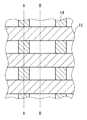
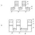
上記従来技術(従来技術1)について図1、図2を用い説明する。図1は従来技術1に係るフラッシュメモリの上視図。図2はその断面図であり、図2(a)は図1のA−A断面図、図2(b)は図1のB−B断面図である。図1を参照に、ビットライン14が図1の縦方向に延在しており、ワードライン15がビットラインの幅方向に延在している。 The prior art (prior art 1) will be described with reference to FIGS. FIG. 1 is a top view of a flash memory according to Prior Art 1. FIG. 2 is a cross-sectional view thereof, FIG. 2 (a) is a cross-sectional view taken along line AA of FIG. 1, and FIG. 2 (b) is a cross-sectional view taken along line BB of FIG. Referring to FIG. 1,
図2を参照に、半導体基板10にソース領域およびドレイン領域を兼ねるビットライン14が埋め込まれている。半導体基板10上にはONO膜12が形成されている。ONO膜12上にゲート電極を兼ねるワードライン15が形成されている。 Referring to FIG. 2, a
ビットライン14間(ソース領域とドレイン領域間)のワードライン15(ゲート電極)下の半導体基板10がチャネルとなる。チャネル上のONO膜12に電荷を蓄積することにより不揮発性メモリとして機能する。 The
特許文献1および特許文献2には、ビットライン14間であってワードライン15間の半導体基板10にトレンチ部を設けた半導体装置において、ビットライン上に熱酸化シリコン膜が形成された技術が開示されている。ワードラインを形成する際、ビットライン上の熱酸化シリコン膜をマスクに、半導体基板にトレンチ凹部を設けるものである。 Patent Documents 1 and 2 disclose a technique in which a thermal silicon oxide film is formed on a bit line in a semiconductor device in which a trench portion is provided in the
特許文献1では、チャネル上のゲート電極構造はワードラインの1層である(従来技術2)。一方、特許文献2では、チャネル上のゲート電極構造は、フロチィングゲート、酸化シリコン膜およびコントロールゲート(ワードライン)である(従来技術3)。 In Patent Document 1, the gate electrode structure on the channel is one layer of word lines (conventional technique 2). On the other hand, in Patent Document 2, the gate electrode structure on the channel is a floating gate, a silicon oxide film, and a control gate (word line) (prior art 3).
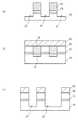
図3は従来技術1における課題を説明するための図である。図3(a)は従来技術1に係るフラッシュメモリの上視図であり、図3(b)はそのB−B断面図である。図3(a)を参照に、従来技術1において、ONO膜12への電荷の書き込みは、ビットライン14間に高電圧を引加し、ワードライン15(ゲート電極)下のチャネル50で高エネルギとなった電荷をONO膜12中のトラップ層にトラップさせることにより行う。 FIG. 3 is a diagram for explaining a problem in the prior art 1. 3A is a top view of the flash memory according to the related art 1, and FIG. 3B is a cross-sectional view taken along the line BB. Referring to FIG. 3A, in the prior art 1, in the charge writing to the
しかしながら、ワードライン15下の半導体基板10中の電流は、図3(a)の破線矢印のように、ワードライン15下のチャネル50の両側にも流れてしまう。図3(b)では、ワードライン15下のチャネル50の両側にチャネルが拡大する(符号52)。このため、図3(a)のように、ワードライン15下のONO膜12に電荷がトラップされる(符号54)だけでなく、ワードライン15の両側のONO膜12にも電荷がトラップされる(符号54a) However, the current in the
このように、ワードライン15の両側のONO膜12中に電荷がトラップされると、以下の課題が生じる。まず、消去動作時に電荷を消去できない。さらに、隣のワードライン15下のONO膜12中に電荷がトラップしてしまう。これらにより、メモリセルが誤動作するという課題も生じる。このため、ワードライン15間隔を狭くしメモリセルの微細化を行うことが困難であった。 As described above, when charges are trapped in the ONO
そこで、従来技術2および3のように、ビットライン14間であってワードライン15間の半導体基板10にトレンチ部を設けることが考えられる。しかし、従来技術2および3のように、ビットライン上に熱酸化シリコン膜を設ける構造(LOCOS構造)では、バードビークが生じ微細化が難しい。また、従来技術3ではコントロールゲートとフローテキングゲートの間に酸化膜層が設けてあるため、フローティングゲート、コントロールゲートおよびトレンチ部を形成するエッチングが複雑となる。トレンチ部を形成するためのエッチングの際、ビットライン上の酸化膜をマスクとして使用しているためである。 Therefore, it is conceivable to provide a trench portion in the
本発明は、ワードライン間の素子分離を行い、メモリセルの微細化が可能な半導体装置およびその製造方法を提供することを目的とする。 An object of the present invention is to provide a semiconductor device capable of miniaturizing a memory cell by performing element isolation between word lines and a manufacturing method thereof.
本発明は、半導体基板内に形成されたビットラインと、前記ビットライン上に前記ビットラインの長手方向に連続して設けられた絶縁膜ラインと、前記ビットライン間の前記半導体基板上に設けられたゲート電極と、前記ゲート電極上に接して設けられ、前記ビットラインの幅方向に延在したワードラインと、前記ビットライン間であり前記ワードライン間の前記半導体基板に形成されたトレンチ部と、を具備する半導体装置である。本発明によれば、トレンチ部を設けることにより、ワードラインの両側の半導体基板に電流が流れることはない。これより、ワードライン両側のONO膜に電荷がトラップされることはない。よって、ワードライン間隔を狭くすることができ、メモリセルの微細化が可能な半導体装置を提供することができる。 The present invention is provided on a bit line formed in a semiconductor substrate, an insulating film line continuously provided on the bit line in a longitudinal direction of the bit line, and the semiconductor substrate between the bit lines. A gate electrode provided on and in contact with the gate electrode and extending in a width direction of the bit line, and a trench portion formed in the semiconductor substrate between the bit lines and between the word lines. , A semiconductor device comprising: According to the present invention, by providing the trench portion, no current flows through the semiconductor substrate on both sides of the word line. As a result, charges are not trapped in the ONO films on both sides of the word line. Therefore, it is possible to provide a semiconductor device in which a word line interval can be narrowed and a memory cell can be miniaturized.
本発明は、前記絶縁膜ラインの幅方向側面は、前記半導体基板の表面に対し、概垂直である半導体装置とすることができる。本発明によれば、バーズビークが発生することなく、メモリセルの微細化が可能となる。 The present invention can be a semiconductor device in which the side surface in the width direction of the insulating film line is substantially perpendicular to the surface of the semiconductor substrate. According to the present invention, memory cells can be miniaturized without occurrence of bird's beaks.
本発明は、前記絶縁膜ラインは、酸化シリコン膜を含む半導体装置とすることができる。本発明によれば、半導体基板にトレンチ部を形成する際、シリコン半導体基板とのエッチングの選択比を大きくすることができる。 In the present invention, the insulating film line may be a semiconductor device including a silicon oxide film. According to the present invention, when the trench portion is formed in the semiconductor substrate, the etching selectivity with respect to the silicon semiconductor substrate can be increased.
本発明は、前記トレンチ部上に設けられた絶縁膜層を具備する半導体装置とすることができる。本発明によれば、チャネル間を確実に素子分離することができる。 The present invention can be a semiconductor device including an insulating film layer provided on the trench portion. According to the present invention, elements can be reliably separated between channels.
本発明は、前記トレンチ部と前記絶縁膜層の間に設けられたバリア層を具備し、前記絶縁膜層は窒化シリコン膜を含み、前記バリア層は酸化シリコン膜を含み半導体装置とすることができる。本発明によれば、窒化シリコン膜のストレスによる剥がれ等を防止することができる。さらに、窒化シリコン膜中の水素がONO膜に拡散し、特性が劣化することを防止することができる。 The present invention includes a barrier layer provided between the trench portion and the insulating film layer, the insulating film layer including a silicon nitride film, and the barrier layer including a silicon oxide film as a semiconductor device. it can. According to the present invention, it is possible to prevent the silicon nitride film from being peeled off due to stress. Further, it is possible to prevent hydrogen in the silicon nitride film from diffusing into the ONO film and deteriorating characteristics.
本発明は、前記トレンチ部の半導体基板内に、ビットラインと反対導電型のチャネルカット領域が形成された半導体装置とすることができる。本発明によれば、チャネル間の素子分離をより確実に行うことができる。 The present invention can be a semiconductor device in which a channel cut region having a conductivity type opposite to the bit line is formed in the semiconductor substrate of the trench portion. According to the present invention, element isolation between channels can be more reliably performed.
本発明は、前記トレンチ部の側面に形成された側壁を具備する半導体装置とすることができる。本発明によれば、チャネルカット領域とチャネルの距離を確保することができるため、P型領域からの空乏層により、チャネルが狭くなることを防止することができる。 The present invention can be a semiconductor device including a side wall formed on a side surface of the trench portion. According to the present invention, since the distance between the channel cut region and the channel can be secured, it is possible to prevent the channel from becoming narrow due to the depletion layer from the P-type region.
本発明は、前記半導体基板と前記ゲート電極の間に設けられたONO膜を具備する半導体装置とすることができる。本発明によれば、ONO膜を有するフラッシュメモリにおいて、ワードライン両側のONO膜への電荷のトラップを抑制することができる。 The present invention can be a semiconductor device including an ONO film provided between the semiconductor substrate and the gate electrode. According to the present invention, in a flash memory having an ONO film, trapping of charges in the ONO film on both sides of the word line can be suppressed.
本発明は、半導体基板内のビットラインを形成する工程と、前記ビットライン上に前記ビットラインの長手方向に連続して形成された絶縁膜ラインを形成する工程と、前記ビットライン間の前記半導体基板上にゲート電極を形成する工程と、前記ゲート電極上に接して設けられ、前記ビットラインの幅方向に延在するワードラインを形成する工程と、前記ビットライン間であり前記ワードライン間の前記半導体基板に、トレンチ部を形成する工程と、を有し、前記トレンチ部を形成する工程は、少なくとも前記絶縁膜ラインをマスクに前記半導体基板をエッチングする工程を含む半導体装置の製造方法である。本発明によれば、トレンチ部を形成することにより、ワードラインの両側の半導体基板に電流が流れることはない。これより、ワードライン両側のONO膜に電荷がトラップされることはない。よって、ワードライン間隔を狭くすることができ、メモリセルの微細化が可能な半導体装置の製造方法を提供することができる。 The present invention includes a step of forming a bit line in a semiconductor substrate, a step of forming an insulating film line continuously formed in the longitudinal direction of the bit line on the bit line, and the semiconductor between the bit lines. Forming a gate electrode on the substrate; forming a word line in contact with the gate electrode and extending in a width direction of the bit line; and between the bit lines and between the word lines Forming a trench portion in the semiconductor substrate, and the step of forming the trench portion includes a step of etching the semiconductor substrate using at least the insulating film line as a mask. . According to the present invention, by forming the trench portion, no current flows through the semiconductor substrate on both sides of the word line. As a result, charges are not trapped in the ONO films on both sides of the word line. Therefore, it is possible to provide a method for manufacturing a semiconductor device in which the word line interval can be narrowed and the memory cells can be miniaturized.
本発明は、前記ビットラインを形成する工程は、前記ゲート電極を構成すべき第1の金属層に形成された開口部の前記半導体基板に、イオン注入を行う工程を含み、前記絶縁膜ラインを形成する工程は、前記開口部および前記第1の金属層上に絶縁膜ライン層を堆積する工程と、前記絶縁膜ライン層を前記第1の金属層まで研磨する工程と、を含む半導体装置の製造方法とすることができる。本発明によれば、ビットラインと絶縁膜ラインをセルフアラインで形成することができる。よって、絶縁膜ラインをビットラインの長手方向に連続して形成することができる。また、絶縁膜ラインを第1の金属層の開口部内に形成することにより、絶縁膜ラインの側面を半導体基板に対し、概垂直とすることができる。これにより、メモリセルの微細化が可能となる。 In the present invention, the step of forming the bit line includes a step of implanting ions into the semiconductor substrate in the opening formed in the first metal layer that constitutes the gate electrode, and the insulating film line is formed. The step of forming includes: a step of depositing an insulating film line layer on the opening and the first metal layer; and a step of polishing the insulating film line layer to the first metal layer. It can be set as a manufacturing method. According to the present invention, the bit line and the insulating film line can be formed by self-alignment. Therefore, the insulating film line can be continuously formed in the longitudinal direction of the bit line. Also, by forming the insulating film line in the opening of the first metal layer, the side surface of the insulating film line can be made substantially perpendicular to the semiconductor substrate. Thereby, the memory cell can be miniaturized.
本発明は、前記絶縁膜ラインを形成する工程は、酸化シリコン膜をCVD法で形成する工程を含む半導体装置の製造方法とすることができる。本発明によれば、バーズビークが発生することがなく、メモリセルの一層の微細化が可能となる。 According to the present invention, the step of forming the insulating film line may be a method for manufacturing a semiconductor device including a step of forming a silicon oxide film by a CVD method. According to the present invention, bird's beak does not occur, and the memory cell can be further miniaturized.
本発明は、前記トレンチ部上に絶縁膜層を形成する工程を有する半導体装置の製造方法とすることができる。本発明によれば、チャネル間をより確実に素子分離することができる。 The present invention can be a method for manufacturing a semiconductor device including a step of forming an insulating film layer on the trench portion. According to the present invention, it is possible to more reliably separate elements between channels.
本発明は、前記トレンチ部上に酸化シリコン膜層を含むバリア層を形成する工程を有し、前記絶縁膜層を形成する工程は、前記バリア層上に窒化シリコン膜層を形成する工程を含む半導体装置の製造方法とすることができる。本発明によれば、窒化シリコン膜のストレスによる剥がれ等を防止することができる。さらに、窒化シリコン膜中の水素がONO膜に拡散し、特性が劣化することを防止することができる。 The present invention includes a step of forming a barrier layer including a silicon oxide film layer on the trench portion, and the step of forming the insulating film layer includes a step of forming a silicon nitride film layer on the barrier layer. It can be set as the manufacturing method of a semiconductor device. According to the present invention, it is possible to prevent the silicon nitride film from being peeled off due to stress. Further, it is possible to prevent hydrogen in the silicon nitride film from diffusing into the ONO film and deteriorating characteristics.
本発明は、前記絶縁膜層の間の前記絶縁膜ラインに、前記ビットラインに接続するコンタクトホールを形成する工程を有する半導体装置の製造方法とすることができる。本発明によれば、コンタクトホールを形成する際、絶縁膜ラインを絶縁膜層に対し選択的にエッチングを行うことができる。これにより、ビットラインとコンタクトホールの露光時の合わせ余裕を確保する必要がなくメモリセルを微細化することができる。 The present invention can be a method for manufacturing a semiconductor device including a step of forming a contact hole connected to the bit line in the insulating film line between the insulating film layers. According to the present invention, when the contact hole is formed, the insulating film line can be selectively etched with respect to the insulating film layer. As a result, it is not necessary to secure an alignment margin when exposing the bit line and the contact hole, and the memory cell can be miniaturized.
本発明は、前記トレンチ部の前記半導体基板に、前記ビットラインと反対導電型のチャネルカット領域を形成する工程を有する半導体装置の製造方法とすることができる。本発明によれば、チャネル間の素子分離をより確実に行うことができる。 The present invention can be a semiconductor device manufacturing method including a step of forming a channel cut region having a conductivity type opposite to the bit line in the semiconductor substrate of the trench portion. According to the present invention, element isolation between channels can be more reliably performed.
本発明は、前記チャネルカット領域を形成する工程は、前記絶縁膜ラインと前記ワードラインをマスクに前記トレンチ部にイオン注入を行う工程を含む半導体装置の製造方法とすることができる。本発明によれば、チャネルカット領域をトレンチ部とセルフアラインに形成することができる。よって、製造工程の削減を行うことができる。また、露光時の合わせずれを考慮する必要がなくメモリセルの微細化を行うことができる。 The present invention may be a method of manufacturing a semiconductor device, wherein the step of forming the channel cut region includes a step of ion implantation into the trench portion using the insulating film line and the word line as a mask. According to the present invention, the channel cut region can be formed in a self-aligned manner with the trench portion. Therefore, the manufacturing process can be reduced. Further, it is not necessary to consider misalignment during exposure, and the memory cell can be miniaturized.
本発明は、前記トレンチ部の側部に側壁を形成する工程を有し、前記チャネルカット領域を形成する工程は、前記絶縁膜ライン、前記ワードライン、および前記側壁をマスクに前記トレンチ部にイオン注入を行う工程を含む半導体装置の製造方法とすることができる。本発明によれば、チャネルカット領域とチャネルの距離を確保することができるため、P型領域からの空乏層により、チャネルが狭くなることを防止することができる。さらに、チャネルカット領域をトレンチ部とセルフアラインに形成することができる。よって、製造工程の削減を行うことができる。また、露光時の合わせずれを考慮する必要がなくメモリセルの微細化を行うことができる。 The present invention includes a step of forming a side wall on a side portion of the trench portion, and the step of forming the channel cut region includes ions formed in the trench portion using the insulating film line, the word line, and the side wall as a mask. It can be set as the manufacturing method of the semiconductor device including the process of implanting. According to the present invention, since the distance between the channel cut region and the channel can be secured, it is possible to prevent the channel from becoming narrow due to the depletion layer from the P-type region. Furthermore, the channel cut region can be formed in a self-aligned manner with the trench portion. Therefore, the manufacturing process can be reduced. Further, it is not necessary to consider misalignment during exposure, and the memory cell can be miniaturized.
本発明は、前記半導体基板上にONO膜を形成する工程を有し、前記ゲート電極を形成する工程は、前記ONO膜上にゲート電極を形成する工程である半導体装置の製造方法とすることができる。本発明によれば、ONO膜を有するフラッシュメモリにおいて、ワードライン両側のONO膜への電荷のトラップを抑制することができる。 The present invention includes a method of manufacturing a semiconductor device, including a step of forming an ONO film on the semiconductor substrate, wherein the step of forming the gate electrode is a step of forming a gate electrode on the ONO film. it can. According to the present invention, in a flash memory having an ONO film, trapping of charges in the ONO film on both sides of the word line can be suppressed.
本発明によれば、ワードライン間の素子分離を行い、メモリセルの微細化が可能な半導体装置およびその製造方法を提供することを目的とする。 According to the present invention, it is an object to provide a semiconductor device and a method for manufacturing the same capable of element isolation between word lines and miniaturization of memory cells.
以下、図面を用い本発明に係る実施例について説明する。 Embodiments according to the present invention will be described below with reference to the drawings.
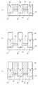
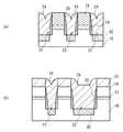
図4は実施例1に係るフラッシュメモリの上視図(保護膜、配線層、層間絶縁膜は図示せず)である。図5(a)は図4のA−A断面図であり、図5(b)は図4のB−B断面図であり、図5(c)は図4のC−C断面図である。図6(a)は図4のD−D断面図であり、図6(b)は図4のE−E断面図である。図4を参照し、P型シリコン半導体基板10(または半導体基板内に形成されたP型領域)内に埋め込まれ形成されたビットライン14およびその上にビットライン14の長手方向に連続して形成された絶縁膜ライン18が図4の縦方向に延在している。さらに、図4では図示していないが、配線層36がビットライン14上をビットライン14の長手方向に延在している。 FIG. 4 is a top view (a protective film, a wiring layer, and an interlayer insulating film are not shown) of the flash memory according to the first embodiment. 5A is a cross-sectional view taken along line AA in FIG. 4, FIG. 5B is a cross-sectional view taken along line BB in FIG. 4, and FIG. 5C is a cross-sectional view taken along line CC in FIG. . 6A is a DD cross-sectional view of FIG. 4, and FIG. 6B is an EE cross-sectional view of FIG. Referring to FIG. 4, a
ワードライン20がビットラインの幅方向に延在している。ワードライン20を複数本越える毎に、コンタクトホールが形成されている。コンタクトホール内はプラグ金属34で埋め込まれており、ビットライン14と配線層36を接続している。これは、ビットライン14は拡散層で形成されているため抵抗が高い。このため、メモリセルの書き込み・消去特性が劣化してしまう。そこで、この劣化を防止するため、ビットライン14はワードライン20を複数本越える毎に、低抵抗の配線層36と接続している。 A
図5(a)を参照に、ワードライン20長手方向のワードライン20間の断面について説明する。ビットライン14間の半導体基板10にトレンチ部22が形成されており、トレンチ部22上に絶縁膜層24として窒化シリコン膜が設けられている。半導体基板10内にビットライン14が埋め込まれている。その上には絶縁膜ライン18として、酸化シリコン膜が設けられている。絶縁膜ライン18および絶縁膜層24上に層間絶縁膜30が設けられている。層間絶縁膜30上のビットライン14上には配線層36が設けられている。それらの上に、保護膜38が設けられている。 A cross section between the word lines 20 in the longitudinal direction of the word lines 20 will be described with reference to FIG. A
図5(b)を参照に、ワードライン20長手方向のワードライン20の断面について説明する。ビットライン14間の半導体基板10にはトレンチ部22が設けられておらず、半導体基板10内にチャネルが形成される。ビットライン14間の半導体基板10上にONO膜12が設けられている。ONO膜12上の絶縁膜ライン18間にゲート電極16が設けられている。半導体基板10内に形成されたビットライン14はソース領域およびドレイン領域として機能する。ビットライン14上には絶縁膜ライン18が設けられている。絶縁膜ライン18およびゲート電極16上にワードライン20が接して設けられている。これにより、ゲート電極16とワードライン20が接続される。ワードライン20上には層間絶縁膜30が設けられ、その上は図5(a)と同じである。 A cross section of the
図5(c)を参照に、ワードライン20長手方向のコンタクトホール32を横切る断面について説明する。ビットライン14間は図5(a)と同様であり、説明を省略する。ビットライン14上にはコンタクトホールが形成され、プラグ金属34が埋め込まれている。プラグ金属34上に配線層36が設けられ、ビットライン14と配線層36がコンタクトホールにより接続している。 With reference to FIG. 5C, a cross section that crosses the
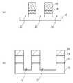
図6(a)を参照に、ビットライン14長手方向のビットライン14間の断面について説明する。ワードライン20間では、半導体基板10にトレンチ部22が形成されており、トレンチ部22上に絶縁膜層24が形成されている。ワードライン20下では、トレンチ部22は形成されておらず、半導体基板10内にチャネルが形成される。半導体基板10上にONO膜12、ONO膜12上にはゲート電極16、ゲート電極16上にワードライン18が設けられている。ワードライン16および絶縁膜層24上に層間絶縁膜30、層間絶縁膜30上に保護膜38が設けられている。 A cross section between the bit lines 14 in the longitudinal direction of the bit lines 14 will be described with reference to FIG. Between the word lines 20, a
図6(b)を参照に、ビットライン14長手方向のビットライン14の断面について説明する。半導体基板10にはビットライン14が埋め込まれ形成されている。ビットライン14上には絶縁膜ライン18が連続して形成されている。絶縁膜ライン18上にワードライン20が設けられている。ワードライン20および絶縁膜ライン18上に層間絶縁膜30が設けられている。層間絶縁膜30上に配線層36が設けられ、配線層36上に保護膜38が設けられている。ビットライン14と配線層36はワードライン20を複数本越える毎に、絶縁膜ライン18および層間絶縁膜30に形成されたコンタクトホール32により接続している。コンタクトホール32にはプラグ金属34が埋め込まれている。 With reference to FIG. 6B, a cross section of the
実施例1に係るフラッシュメモリにおいては、ビットライン14間でありワードライン20間の半導体基板10に形成されたトレンチ部22を具備している。これにより、従来技術1のように、ワードライン20の両側の半導体基板10中に電流が流れることはなく、ワードライン20両側のONO膜12に電荷がトラップされることはない。よって、ワードライン20間隔を狭くすることができ、メモリセルの微細化が可能となる。 The flash memory according to the first embodiment includes a
従来技術2のようにワードラインが1層の場合、絶縁膜ライン18を概垂直な形状とすることが難しい。絶縁膜ライン18間へのワードライン20の埋込性が悪くなるためである。そこで、実施例1のように、ゲート電極16が絶縁膜ライン18間に設けられ、その上にワードライン20を重ねて接するように設ける。これにより、従来技術2の課題を解決することができる。また、ゲート電極16とワードライン20が接して設けられている。これにより、後の製造方法の説明で述べるように、トレンチ部22を形成する際、従来技術3のように、複雑なエッチングをする必要がなくなる。 When the word line is a single layer as in prior art 2, it is difficult to make the insulating
従来技術2および3のように絶縁膜ラインを熱酸化膜で形成すると、絶縁膜ライン18の側面は斜面となり、バーズビークによりチャネル幅が狭くなり、メモリセルの微細化が難しい。そこで、実施例1のように、絶縁膜ライン18の幅方向側面を、半導体基板10の表面に対し概垂直とすることが好ましい。概垂直とは、LOCOS構造の熱酸化シリコン膜を形成したのに比べ垂直に形成すことである。これにより、バーズビークが発生することなく、メモリセルの微細化が可能となる。 When the insulating film line is formed of a thermal oxide film as in the prior arts 2 and 3, the side surface of the insulating
また、絶縁膜ライン18は絶縁性があればよいが、実施例1のように絶縁膜ライン18は酸化シリコン膜を含むことが好ましい。これにより、トレンチ部22を形成する際、シリコン半導体基板10とのエッチングの選択比を大きくすることができる。 The insulating
さらに、実施例1のようにトレンチ部22上に絶縁膜層24を設けることが好ましい。これにより、チャネル間を確実に絶縁することができる。また、実施例1のように絶縁膜ライン18を酸化シリコン膜、絶縁膜層22を窒化シリコン膜とすることにより、酸化シリコン膜を窒化シリコン膜に対し選択的にエッチングを行うことができる。これにより、ビットライン14とコンタクトホールの露光時の合わせ余裕を確保する必要がなくメモリセルを微細化することができる。 Further, it is preferable to provide the insulating
さらに、半導体基板10とゲート電極16の間にONO膜12を設けられている。このように、ONO膜12を有するフラッシュメモリにおいて、ワードライン20両側のONO膜12への電荷のトラップを抑制することができる。 Further, an
次に、図7ないし図12を用い実施例1に係るフラッシュメモリの製造方法について説明する。図7ないし図11は、各図(a)が図4のA−A断面に相当する断面図であり、各図(b)が図4のB−B断面に相当する断面図であり、各図(c)が図4のD−D断面に相当する断面図である。図12は図4のC−C断面に相当する断面図である。 Next, a method for manufacturing the flash memory according to the first embodiment will be described with reference to FIGS. 7 to 11 are cross-sectional views corresponding to the AA cross section of FIG. 4 and FIGS. 7B to 11B are cross-sectional views corresponding to the BB cross section of FIG. FIG. 7C is a cross-sectional view corresponding to the cross section DD in FIG. 12 is a cross-sectional view corresponding to the CC cross section of FIG.
図7を参照し、P型シリコン半導体基板10(または半導体基板内のP型領域)上にONO膜12として、トンネル酸化膜(酸化シリコン膜)を熱酸化法で、トラップ層(窒化シリコン膜)、トップ酸化膜(酸化シリコン膜)をCVD法で形成する。ONO膜12上に、ゲート電極16を構成すべき第1の金属層16aとして多結晶シリコン膜を形成する。第1の金属層16a上にビットライン14を形成する領域に開口部を設けたフォトレジスト44を形成する。フォトレジスト44をマスクに第1の金属層16aおよびONO膜12をエッチングし、開口部48を形成する。これにより、図7(a)および(b)のように、ビットライン14および絶縁膜ライン18を形成すべき領域に開口部48が形成される。図7(c)のように、ビットライン14が形成されるビットライン14間には連続して、第1の金属層16aが設けられている。開口部48の側面は、半導体基板10の表面に対し概垂直に形成する。なお、第1の金属層16aの膜厚は100nm、開口部48の幅(すなわちビットライン幅)は
70nm、ビットライン間距離は160nmである。Referring to FIG. 7, a tunnel oxide film (silicon oxide film) is formed as a
図8を参照し、フォトレジスト44をマスクに半導体基板10に例えば砒素をイオン注入し、フォトレジスト44を除去する。その後熱処理することにより、半導体基板10内にN型のビットライン14を形成する。高密度プラズマ型のCVD装置により、開口部48を埋め込むように、開口部48と第1の金属層16a上に、約180nmの膜厚を有する酸化シリコン膜層を堆積させる。高密度プラズマ型のCVD装置を用いることにより、アスペクト比が2.7と大きい開口部48にも確実に酸化シリコン膜18を埋め込むことができる。CMP法を用い、酸化シリコン膜層を第1の金属層16aまで研磨する。これにより、ビットライン14上に開口部48に埋め込まれた絶縁膜ライン18が形成される。なお、このとき、第1の金属層16aの膜厚は約90nmとなる。 Referring to FIG. 8, arsenic ions, for example, are implanted into
このように、ビットライン14と絶縁膜ライン18がセルフアラインで形成することができる。よって、絶縁膜ライン18をビットライン14の長手方向に連続して形成することができる。また、絶縁膜ライン18を開口部48内に形成することにより、絶縁膜ライン18の側面を半導体基板10に対し、概垂直とすることができる。これにより、メモリセルの微細化が可能となる。さらに、CVD法により絶縁膜ラインを形成することにより、バーズビークが発生することがなく、メモリセルの一層の微細化が可能となる。 Thus, the
図9を参照し、絶縁膜ライン18および第1の金属層16a上にワードライン20を構成すべき第2の金属層20aを多結晶シリコン膜を用い形成する。第2の金属層20a上に、ワードライン20を形成する領域以外に開口部を設けたフォトレジスト46を形成する。図9(a)のように、ワードライン12間となるべき領域にはフォトレジスト46は形成されておらず、図9(b)のように、ワードライン12となるべき領域にはフォトレジスト46が形成される。なお、第2の金属層20aの膜厚(すなわちワードラインの膜厚)は100nm、ワードライン幅は75nm、ワードライン間隔は75nmである。 Referring to FIG. 9, a
図10を参照し、フォトレジスト46をマスクに、第2の金属層20a、第1の金属層16aおよびONO膜12をエッチングする。さらに、ビットライン14間でありワードライン20間の半導体基板10に深さ40nmのトレンチ部22を形成する。このとき、図10(a)のように、ワードライン20間の領域では、第2の金属層20aおよびビットライン14間の第1の金属層16aがエッチングされる。さらに、ビットライン14間の半導体基板10にトレンチ部22が形成される。ビットライン14上には絶縁膜ライン18が設けてある。絶縁膜ライン18は、酸化シリコン膜で構成されている。そこで、酸化シリコン膜に対し多結晶シリコン膜等からなる第2の金属層20aおよび第1の金属層16aを選択的にエッチングすることにより、絶縁膜ライン18を残存させることができる。これにより、半導体基板10にトレンチ部22を形成する際も、ビットライン14がエッチングされることを防止することができる。 Referring to FIG. 10,
図10(b)のように、ワードライン20を形成する領域は第1の金属層16aおよび第2の金属層20aが残存し、ゲート電極16およびワードライン20となる。よって、ビットライン14間の半導体基板10上にゲート電極16が形成され、ゲート電極16に接し、ビットライン14幅方向に延在するワードライン20が形成される。さらに、ビットライン14の間でありワードライン20の間の半導体基板10にトレンチ部22が形成される。トレンチ部22の形成は少なくとも絶縁膜ライン18をマスクに半導体基板10をエッチングすることにより形成される。 As shown in FIG. 10B, the
従来技術3のように、第1の金属層16aと第2の金属層20aの間に酸化シリコン膜がある場合、第2の金属膜20aエッチング後、この酸化シリコン膜で停止してしまうか、エッチングに時間がかかってしまう。そこで、酸化シリコン膜のエッチングを別条件で行い、さらに、第1の金属層16aをエッチングする必要があった。実施例1では、ゲート電極16上にワードライン20、すなわち第1の金属層16a上に第2の金属層20aを接して設けることにより、ONO膜12まで、連続してエッチングを行うことができ、上記複雑なエッチングは必要としない。 If there is a silicon oxide film between the
以上、説明したように、第1の金属層16aに形成された開口部48により、ビットライン14と絶縁膜ライン18をセルフアラインで形成する。さらに、その上に、第2の金属層20aを形成する。そして、ワードライン20、ゲート電極16およびトレンチ部22を形成するためのエッチングを、同一のマスクを用い行う。これにより、ワードライン20、ゲート金属16およびトレンチ部22がセルフアラインで形成できる。よって、製造工程の削減を行うことができる。さらに、露光時の合わせずれを考慮する必要がなくメモリセルの微細化を行うことができる。 As described above, the
図11を参照し、トレンチ部22上に、トレンチ部22を埋め込むように絶縁膜層24として膜厚100nmの窒化シリコン膜をCVD法または高密度プラズマ型のCVD装置で形成する。その後、全面をエッチングする、またはCMP法を用い研磨することにより、絶縁膜層24が埋め込まれる。絶縁膜層24により、ワードライン20下のチャネル間をより確実に素子分離することができる。 Referring to FIG. 11, a 100 nm-thickness silicon nitride film is formed as an insulating
次に、図12を参照し、コンタクトホール32を形成する領域について説明する。図12(a)は図11と同じ製造工程の図である。コンタクトホールを形成する前は、図4のA−A断面に相当する図11(a)と同じ構成の断面となる。図12(b)を参照し、絶縁膜層24および絶縁膜ライン18上に層間絶縁膜30として例えばBPSG(Boro-Phospho Silicated Glass)等の酸化シリコン膜をCVD法を用い形成する。フォトレジストをマスクに、層間絶縁膜30および絶縁膜層24の間の絶縁膜ライン18をエッチングし、ビットライン14に接続するコンタクトホール32を形成する。 Next, a region where the
層間絶縁膜30および絶縁膜ライン18は酸化シリコン膜であり、絶縁膜層24は窒化シリコン膜である。そのため、酸化シリコン膜を窒化シリコン膜に対し選択的にエッチングを行うことができる。これにより、コンタクトホール32を形成するフォトレジストの開口部がビットライン14からずれた場合であっても、コンタクトホール32がビットライン14から外れて形成されることはない。コンタクトホール32がビットライン14から外れて形成されると、ビットライン14と半導体基板10間に接合電流が流れしまう。実施例1ではこれを防止することができる。これにより、ビットライン14とコンタクトホールの露光時の合わせ余裕を確保する必要がなくメモリセルを微細化することができる。 The
図12(c)を参照し、コンタクトホール32内に、例えばTi/WNまたはTi/TiN並びにW等の金属を埋め込み、プラグ金属34を形成する。その後、配線層36の形成、保護膜38の形成を行い、実施例1にかかるフラッシュメモリが完成する。 Referring to FIG. 12C, a metal such as Ti / WN or Ti / TiN and W is embedded in the
実施例2は絶縁膜層24の底部および側部にバリア層を設けた例である。図13ないし図15は実施例2に係るフラッシュメモリの製造方法を示す図である。各図(a)は図4のA−A断面に相当する断面図であり、各図(b)は図4のD−D断面に相当する断面図である。図13において、実施例1と同様に図10までの製造工程を行う。実施例1と同じ構成要素は同じ符号を付し、説明を省略する。図14を参照し、トレンチ部22の上および側面、並びにONO膜12、絶縁膜ライン18、ゲート電極16およびワードライン20の側面に酸化シリコン膜層を含むバリア層26をCVD法で形成する。バリア層26の膜厚は30nmである。バリア層26上に絶縁膜層24として窒化シリコン膜層をCVD法または高密度プラズマ型のCVD装置で形成する。その後、全面をエッチングする、またはCMP法を用い研磨することにより、絶縁膜層24およびバリア層26が埋め込まれる。その後、実施例1の図12と同じ工程を行うことにより実施例2に係るフラッシュメモリが完成する。 Example 2 is an example in which a barrier layer is provided on the bottom and sides of the insulating
実施例2に係るフラッシュメモリは実施例1と同様の効果を得ることができる。加えて、実施例2に係るフラッシュメモリは、トレンチ部22と窒化シリコン膜である(含む)絶縁膜層24の間に設けられた酸化シリコン膜である(を含む)バリア層26を具備している。これにより、窒化シリコン膜のストレスによる剥がれ等を防止することができる。さらに、窒化シリコン膜中の水素がONO膜12に拡散し、特性が劣化することを防止することができる。バリア層26は、剥がれ防止の目的としては少なくともトレンチ部22上に形成され、ONO膜12とのバリアの目的としては、少なくともONO膜12の側面に形成されていることが好ましい。 The flash memory according to the second embodiment can obtain the same effects as those of the first embodiment. In addition, the flash memory according to the second embodiment includes a barrier layer 26 (including) a silicon oxide film provided between the
実施例3はトレンチ部22にチャネルカット領域40を設けた例である。図16および図17は実施例3に係るフラッシュメモリの製造方法を示す図である。各図(a)は図4のA−A断面に相当する断面図であり、各図(b)は図4のD−D断面に相当する断面図である。図16を参照し、まず、実施例1と同様に図10までの製造工程を行う。実施例1と同じ構成要素は同じ符号を付し、説明を省略する。その後、絶縁膜ライン18およびワードライン20をマスクに、トレンチ部22の半導体基板10に例えばボロンをイオン注入し、P型(ビットライン14と反対導電型)のチャネルカット領域40を形成する。イオン注入は、例えば注入エネルギ65keV、ドーズ量1E13cm−3で行う。The third embodiment is an example in which the channel cut
図17を参照に、実施例1の図11と同様に、トレンチ部22上に絶縁膜層24として窒化シリコン膜を形成する。その後、実施例1の図12と同じ工程を行うことにより実施例3に係るフラッシュメモリが完成する。 Referring to FIG. 17, a silicon nitride film is formed as an insulating
実施例3に係るフラッシュメモリは実施例1と同様の効果を得ることができる。加えて、実施例3に係るフラッシュメモリは、トレンチ部22にP型のチャネルカット領域40を有するため、ワードライン20下のチャネル間の素子分離をより確実に行うことができる。さらに、絶縁膜ライン18およびワードライン20をマスクにチャネルカット領域40を形成しているため、チャネルカット領域40をトレンチ部22とセルフアラインに形成することができる。よって、製造工程の削減を行うことができる。また、露光時の合わせずれを考慮する必要がなくメモリセルの微細化を行うことができる。 The flash memory according to the third embodiment can obtain the same effects as those of the first embodiment. In addition, since the flash memory according to the third embodiment has the P-type
実施例4はトレンチ部22の側面に側壁28を形成し、チャネルカット領域40を設けた例である。図18および図19は実施例4に係るフラッシュメモリの製造方法を示す図である。各図(a)は図4のA−A断面に相当する断面図であり、各図(b)は図4のD−D断面に相当する断面図である。図18を参照し、まず、実施例1と同様に図10までの製造工程を行う。実施例1と同じ構成要素は同じ符号を付し、説明を省略する。その後、サイドウォール法を用い、トレンチ部22の側面に側壁28を形成する。側壁28の幅は、例えば15nmとする。側壁28は例えば酸化シリコン膜または窒化シリコン膜で形成する。絶縁膜ライン18、ワードライン20および側壁28をマスクに、半導体基板10に例えばボロンを実施例3と同じ条件でイオン注入し、その後熱処理する。これにより、P型(ビットライン14と反対導電型)のチャネルカット領域40を形成する。 The fourth embodiment is an example in which the
図19を参照に、実施例1の図11と同様に、トレンチ部22上に絶縁膜層24として窒化シリコン膜を形成する。その後、実施例1の図12と同じ工程を行うことにより実施例4に係るフラッシュメモリが完成する。 Referring to FIG. 19, a silicon nitride film is formed as an insulating
実施例4に係るフラッシュメモリは実施例3と同様の効果を得ることができる。加えて、実施例4に係るフラッシュメモリは、チャネルカット領域40とチャネルの距離を確保することができるため、P型領域からの空乏層により、チャネルが狭くなることを防止することができる。さらに、絶縁膜ライン18、ワードライン20および側壁28をマスクにチャネルカット領域40を形成しているため、チャネルカット領域40をトレンチ部22とセルフアラインに形成することができる。よって、製造工程の削減を行うことができる。また、露光時の合わせずれを考慮する必要がなくメモリセルの微細化を行うことができる。 The flash memory according to the fourth embodiment can obtain the same effects as those of the third embodiment. In addition, since the distance between the channel cut
なお、実施例2のようにバリア層26を有するフラッシュメモリに、実施例3または実施例4のようなチャネルカット領域40を設けることもできる。 Note that the channel cut
以上、本発明の好ましい実施例について詳述したが、本発明は係る特定の実施例に限定されるものではなく、特許請求の範囲に記載された本発明の要旨の範囲内において、種々の変形・変更が可能である。
The preferred embodiments of the present invention have been described in detail above, but the present invention is not limited to the specific embodiments, and various modifications can be made within the scope of the gist of the present invention described in the claims.・ Change is possible.
Claims (18)
Translated fromJapanese前記ビットライン上に前記ビットラインの長手方向に連続して設けられた絶縁膜ラインと、
前記ビットライン間の前記半導体基板上に設けられたゲート電極と、
前記ゲート電極上に接して設けられ、前記ビットラインの幅方向に延在したワードラインと、
前記ビットライン間であり前記ワードライン間の前記半導体基板に形成されたトレンチ部と、を具備する半導体装置。A bit line formed in a semiconductor substrate;
An insulating film line continuously provided on the bit line in the longitudinal direction of the bit line;
A gate electrode provided on the semiconductor substrate between the bit lines;
A word line provided on and in contact with the gate electrode and extending in a width direction of the bit line;
And a trench portion formed in the semiconductor substrate between the bit lines and between the word lines.
前記絶縁膜層は窒化シリコン膜を含み、前記バリア層は酸化シリコン膜を含む請求項4記載の半導体装置。Comprising a barrier layer provided between the trench part and the insulating film layer;
The semiconductor device according to claim 4, wherein the insulating film layer includes a silicon nitride film, and the barrier layer includes a silicon oxide film.
前記ビットライン上に前記ビットラインの長手方向に連続して形成された絶縁膜ラインを形成する工程と、
前記ビットライン間の前記半導体基板上にゲート電極を形成する工程と、
前記ゲート電極上に接して設けられ、前記ビットラインの幅方向に延在するワードラインを形成する工程と、
前記ビットライン間であり前記ワードライン間の前記半導体基板に、トレンチ部を形成する工程と、を有し、
前記トレンチ部を形成する工程は、少なくとも前記絶縁膜ラインをマスクに前記半導体基板をエッチングする工程を含む半導体装置の製造方法。Forming a bit line in the semiconductor substrate;
Forming an insulating film line continuously formed in the longitudinal direction of the bit line on the bit line;
Forming a gate electrode on the semiconductor substrate between the bit lines;
Forming a word line provided in contact with the gate electrode and extending in a width direction of the bit line;
Forming a trench portion in the semiconductor substrate between the bit lines and between the word lines,
The step of forming the trench includes a step of etching the semiconductor substrate using at least the insulating film line as a mask.
前記絶縁膜ラインを形成する工程は、前記開口部および前記第1の金属層上に絶縁膜ライン層を堆積する工程と、前記絶縁膜ライン層を前記第1の金属層まで研磨する工程と、を含む請求項9記載の半導体装置の製造方法。The step of forming the bit line includes a step of implanting ions into the semiconductor substrate in the opening formed in the first metal layer that constitutes the gate electrode,
Forming the insulating film line includes depositing an insulating film line layer on the opening and the first metal layer; and polishing the insulating film line layer to the first metal layer; A method for manufacturing a semiconductor device according to claim 9.
前記絶縁膜層を形成する工程は、前記バリア層上に窒化シリコン膜層を形成する工程を含む請求項12記載の半導体装置の製造方法。Forming a barrier layer including a silicon oxide film layer on the trench portion;
The method of manufacturing a semiconductor device according to claim 12, wherein the step of forming the insulating film layer includes a step of forming a silicon nitride film layer on the barrier layer.
前記チャネルカット領域を形成する工程は、前記絶縁膜ライン、前記ワードライン、および前記側壁をマスクに前記トレンチ部にイオン注入を行う工程を含む請求項15記載の半導体装置の製造方法。Forming a side wall on the side of the trench portion;
The method of manufacturing a semiconductor device according to claim 15, wherein the step of forming the channel cut region includes a step of performing ion implantation into the trench portion using the insulating film line, the word line, and the side wall as a mask.
18. The semiconductor according to claim 9, further comprising a step of forming an ONO film on the semiconductor substrate, wherein the step of forming the gate electrode is a step of forming a gate electrode on the ONO film. Device manufacturing method.
Applications Claiming Priority (1)
| Application Number | Priority Date | Filing Date | Title |
|---|---|---|---|
| PCT/JP2005/011814WO2007000808A1 (en) | 2005-06-28 | 2005-06-28 | Semiconductor device and fabrication method thereof |
Related Child Applications (1)
| Application Number | Title | Priority Date | Filing Date |
|---|---|---|---|
| JP2012151532ADivisionJP5657612B2 (en) | 2012-07-05 | 2012-07-05 | Semiconductor device and manufacturing method thereof |
Publications (1)
| Publication Number | Publication Date |
|---|---|
| JPWO2007000808A1true JPWO2007000808A1 (en) | 2009-01-22 |
Family
ID=37567137
Family Applications (1)
| Application Number | Title | Priority Date | Filing Date |
|---|---|---|---|
| JP2007523257APendingJPWO2007000808A1 (en) | 2005-06-28 | 2005-06-28 | Semiconductor device and manufacturing method thereof |
Country Status (7)
| Country | Link |
|---|---|
| US (2) | US7880218B2 (en) |
| EP (1) | EP1898460B1 (en) |
| JP (1) | JPWO2007000808A1 (en) |
| KR (1) | KR100952718B1 (en) |
| CN (1) | CN101203954B (en) |
| TW (1) | TW200707647A (en) |
| WO (1) | WO2007000808A1 (en) |
Families Citing this family (4)
| Publication number | Priority date | Publication date | Assignee | Title |
|---|---|---|---|---|
| KR101085630B1 (en)* | 2010-12-15 | 2011-11-22 | 주식회사 하이닉스반도체 | Pattern formation method of semiconductor device |
| CN102569204B (en)* | 2010-12-31 | 2014-05-07 | 中芯国际集成电路制造(上海)有限公司 | Memory and manufacturing method thereof |
| CN105762114B (en)* | 2014-12-18 | 2019-01-22 | 中芯国际集成电路制造(上海)有限公司 | The forming method of semiconductor structure |
| CN109659275B (en)* | 2017-10-10 | 2020-11-03 | 联华电子股份有限公司 | Method for manufacturing dynamic random access memory |
Citations (10)
| Publication number | Priority date | Publication date | Assignee | Title |
|---|---|---|---|---|
| JPS5513904A (en)* | 1978-07-17 | 1980-01-31 | Hitachi Ltd | Semiconductor device and its manufacturing method |
| JPS55105375A (en)* | 1978-11-27 | 1980-08-12 | Texas Instruments Inc | Nonnvolatile semiconductor memory element and method of fabricating same |
| JPS63170969A (en)* | 1986-03-27 | 1988-07-14 | テキサス インスツルメンツ インコ−ポレイテツド | Nonvolatile memory |
| JPS6474761A (en)* | 1987-09-17 | 1989-03-20 | Matsushita Electronics Corp | Nonvolatile storage element |
| JPH03125460A (en)* | 1989-10-09 | 1991-05-28 | Matsushita Electric Ind Co Ltd | Manufacturing method of semiconductor device |
| US5168334A (en)* | 1987-07-31 | 1992-12-01 | Texas Instruments, Incorporated | Non-volatile semiconductor memory |
| JP2000286349A (en)* | 1999-03-31 | 2000-10-13 | Sony Corp | Semiconductor device and manufacture thereof |
| US6645801B1 (en)* | 2001-10-01 | 2003-11-11 | Advanced Micro Devices, Inc. | Salicided gate for virtual ground arrays |
| JP2003338566A (en)* | 2002-05-21 | 2003-11-28 | Fujitsu Ltd | Nonvolatile semiconductor memory device and method of manufacturing the same |
| JP2004529500A (en)* | 2001-05-30 | 2004-09-24 | インフィネオン テクノロジーズ アクチェンゲゼルシャフト | Bit line contact in memory cell array |
Family Cites Families (17)
| Publication number | Priority date | Publication date | Assignee | Title |
|---|---|---|---|---|
| US4892840A (en)* | 1986-03-27 | 1990-01-09 | Texas Instruments Incorporated | EPROM with increased floating gate/control gate coupling |
| JPH05198778A (en) | 1992-01-23 | 1993-08-06 | Sony Corp | Manufacture of nonvolatile semiconductor memory |
| JP3125460B2 (en) | 1992-09-03 | 2001-01-15 | 住友化学工業株式会社 | Laminated molded article and method for producing the same |
| US6201277B1 (en)* | 1993-08-31 | 2001-03-13 | Texas Instruments Incorporated | Slot trench isolation for flash EPROM |
| US5763315A (en)* | 1997-01-28 | 1998-06-09 | International Business Machines Corporation | Shallow trench isolation with oxide-nitride/oxynitride liner |
| US7125763B1 (en)* | 2000-09-29 | 2006-10-24 | Spansion Llc | Silicided buried bitline process for a non-volatile memory cell |
| US6925007B2 (en)* | 2001-10-31 | 2005-08-02 | Sandisk Corporation | Multi-state non-volatile integrated circuit memory systems that employ dielectric storage elements |
| WO2003071606A1 (en)* | 2002-02-21 | 2003-08-28 | Matsushita Electric Industrial Co., Ltd. | Semiconductor storage device and its manufacturing method |
| KR100480604B1 (en)* | 2002-07-24 | 2005-04-06 | 삼성전자주식회사 | Method for fabricating shallow well of semiconductor device by low energy implantation |
| JP2004111874A (en) | 2002-09-20 | 2004-04-08 | Matsushita Electric Ind Co Ltd | Nonvolatile semiconductor memory device and method of manufacturing the same |
| US7390718B2 (en)* | 2004-02-20 | 2008-06-24 | Tower Semiconductor Ltd. | SONOS embedded memory with CVD dielectric |
| US7399674B2 (en)* | 2004-10-22 | 2008-07-15 | Macronix International Co., Ltd. | Method of fabricating NAND-type flash EEPROM without field oxide isolation |
| US7214983B2 (en)* | 2004-11-24 | 2007-05-08 | Macronix International Co., Ltd. | Non-volatile memory and fabricating method thereof |
| US7238569B2 (en)* | 2005-04-25 | 2007-07-03 | Spansion Llc | Formation method of an array source line in NAND flash memory |
| US20060281255A1 (en)* | 2005-06-14 | 2006-12-14 | Chun-Jen Chiu | Method for forming a sealed storage non-volative multiple-bit memory cell |
| US7786512B2 (en)* | 2005-07-18 | 2010-08-31 | Saifun Semiconductors Ltd. | Dense non-volatile memory array and method of fabrication |
| JP5013904B2 (en) | 2007-02-27 | 2012-08-29 | 東海ゴム工業株式会社 | Pipe end joint and pipe end connection structure |
- 2005
- 2005-06-28EPEP05765395Apatent/EP1898460B1/ennot_activeCeased
- 2005-06-28JPJP2007523257Apatent/JPWO2007000808A1/enactivePending
- 2005-06-28CNCN2005800501536Apatent/CN101203954B/ennot_activeExpired - Fee Related
- 2005-06-28KRKR1020077030628Apatent/KR100952718B1/ennot_activeExpired - Fee Related
- 2005-06-28WOPCT/JP2005/011814patent/WO2007000808A1/ennot_activeApplication Discontinuation
- 2006
- 2006-06-28USUS11/478,537patent/US7880218B2/enactiveActive
- 2006-06-28TWTW095123469Apatent/TW200707647A/enunknown
- 2010
- 2010-12-21USUS12/974,754patent/US8530307B2/ennot_activeExpired - Fee Related
Patent Citations (10)
| Publication number | Priority date | Publication date | Assignee | Title |
|---|---|---|---|---|
| JPS5513904A (en)* | 1978-07-17 | 1980-01-31 | Hitachi Ltd | Semiconductor device and its manufacturing method |
| JPS55105375A (en)* | 1978-11-27 | 1980-08-12 | Texas Instruments Inc | Nonnvolatile semiconductor memory element and method of fabricating same |
| JPS63170969A (en)* | 1986-03-27 | 1988-07-14 | テキサス インスツルメンツ インコ−ポレイテツド | Nonvolatile memory |
| US5168334A (en)* | 1987-07-31 | 1992-12-01 | Texas Instruments, Incorporated | Non-volatile semiconductor memory |
| JPS6474761A (en)* | 1987-09-17 | 1989-03-20 | Matsushita Electronics Corp | Nonvolatile storage element |
| JPH03125460A (en)* | 1989-10-09 | 1991-05-28 | Matsushita Electric Ind Co Ltd | Manufacturing method of semiconductor device |
| JP2000286349A (en)* | 1999-03-31 | 2000-10-13 | Sony Corp | Semiconductor device and manufacture thereof |
| JP2004529500A (en)* | 2001-05-30 | 2004-09-24 | インフィネオン テクノロジーズ アクチェンゲゼルシャフト | Bit line contact in memory cell array |
| US6645801B1 (en)* | 2001-10-01 | 2003-11-11 | Advanced Micro Devices, Inc. | Salicided gate for virtual ground arrays |
| JP2003338566A (en)* | 2002-05-21 | 2003-11-28 | Fujitsu Ltd | Nonvolatile semiconductor memory device and method of manufacturing the same |
Also Published As
| Publication number | Publication date |
|---|---|
| EP1898460A4 (en) | 2008-09-10 |
| CN101203954A (en) | 2008-06-18 |
| CN101203954B (en) | 2011-09-28 |
| US8530307B2 (en) | 2013-09-10 |
| TW200707647A (en) | 2007-02-16 |
| WO2007000808A1 (en) | 2007-01-04 |
| KR20080013001A (en) | 2008-02-12 |
| US7880218B2 (en) | 2011-02-01 |
| KR100952718B1 (en) | 2010-04-13 |
| US20120070951A1 (en) | 2012-03-22 |
| EP1898460B1 (en) | 2012-01-04 |
| EP1898460A1 (en) | 2008-03-12 |
| US20060291262A1 (en) | 2006-12-28 |
Similar Documents
| Publication | Publication Date | Title |
|---|---|---|
| JP5191633B2 (en) | Semiconductor device and manufacturing method thereof | |
| CN100517732C (en) | Semiconductor structure and manufacturing method thereof | |
| JP2008098519A (en) | Nonvolatile semiconductor memory | |
| US6855599B2 (en) | Fabrication method of a flash memory device | |
| KR100726908B1 (en) | Semiconductor memory | |
| JP5047786B2 (en) | Manufacturing method of semiconductor device | |
| JPWO2006035503A1 (en) | Semiconductor device and method of manufacturing semiconductor device | |
| JPWO2007000808A1 (en) | Semiconductor device and manufacturing method thereof | |
| US20070196983A1 (en) | Method of manufacturing non-volatile memory device | |
| US8093645B2 (en) | Non-volatile semiconductor memory device | |
| JP5053084B2 (en) | Semiconductor device and manufacturing method thereof | |
| JP5657612B2 (en) | Semiconductor device and manufacturing method thereof | |
| US8779500B2 (en) | Memory device | |
| US7847340B2 (en) | Semiconductor device and method for manufacturing the same | |
| JP5301123B2 (en) | Semiconductor device and manufacturing method thereof | |
| JP2009164504A (en) | Capacitor element, nonvolatile memory device including capacitor element, and manufacturing method thereof | |
| JP4944766B2 (en) | Semiconductor device and manufacturing method thereof | |
| JP4927716B2 (en) | Semiconductor device | |
| JP5443676B2 (en) | Semiconductor device and manufacturing method thereof | |
| JP2008251665A (en) | Nonvolatile semiconductor memory device | |
| JP2006324274A (en) | Nonvolatile semiconductor storage and manufacturing method thereof | |
| JP2004253474A (en) | Nonvolatile semiconductor memory device and method of manufacturing the same | |
| JP5529216B2 (en) | Semiconductor device and manufacturing method of semiconductor device |
Legal Events
| Date | Code | Title | Description |
|---|---|---|---|
| RD04 | Notification of resignation of power of attorney | Free format text:JAPANESE INTERMEDIATE CODE: A7424 Effective date:20100208 | |
| RD03 | Notification of appointment of power of attorney | Free format text:JAPANESE INTERMEDIATE CODE: A7423 Effective date:20100616 | |
| RD03 | Notification of appointment of power of attorney | Free format text:JAPANESE INTERMEDIATE CODE: A7423 Effective date:20100805 | |
| A711 | Notification of change in applicant | Free format text:JAPANESE INTERMEDIATE CODE: A711 Effective date:20100922 | |
| A131 | Notification of reasons for refusal | Free format text:JAPANESE INTERMEDIATE CODE: A131 Effective date:20111108 | |
| A521 | Request for written amendment filed | Free format text:JAPANESE INTERMEDIATE CODE: A523 Effective date:20120207 | |
| A02 | Decision of refusal | Free format text:JAPANESE INTERMEDIATE CODE: A02 Effective date:20120306 | |
| A521 | Request for written amendment filed | Free format text:JAPANESE INTERMEDIATE CODE: A523 Effective date:20120705 | |
| A911 | Transfer to examiner for re-examination before appeal (zenchi) | Free format text:JAPANESE INTERMEDIATE CODE: A911 Effective date:20120820 | |
| RD03 | Notification of appointment of power of attorney | Free format text:JAPANESE INTERMEDIATE CODE: A7423 Effective date:20120831 | |
| A912 | Re-examination (zenchi) completed and case transferred to appeal board | Free format text:JAPANESE INTERMEDIATE CODE: A912 Effective date:20121019 |