JPWO2005091374A1 - Semiconductor device and manufacturing method thereof - Google Patents
Semiconductor device and manufacturing method thereofDownload PDFInfo
- Publication number
- JPWO2005091374A1 JPWO2005091374A1JP2006511276AJP2006511276AJPWO2005091374A1JP WO2005091374 A1JPWO2005091374 A1JP WO2005091374A1JP 2006511276 AJP2006511276 AJP 2006511276AJP 2006511276 AJP2006511276 AJP 2006511276AJP WO2005091374 A1JPWO2005091374 A1JP WO2005091374A1
- Authority
- JP
- Japan
- Prior art keywords
- semiconductor
- semiconductor layer
- region
- semiconductor region
- semiconductor device
- Prior art date
- Legal status (The legal status is an assumption and is not a legal conclusion. Google has not performed a legal analysis and makes no representation as to the accuracy of the status listed.)
- Pending
Links
- 239000004065semiconductorSubstances0.000titleclaimsabstractdescription878
- 238000004519manufacturing processMethods0.000titleclaimsdescription65
- 238000000034methodMethods0.000claimsdescription48
- 238000005530etchingMethods0.000claimsdescription41
- 239000000758substrateSubstances0.000claimsdescription35
- 238000012545processingMethods0.000claimsdescription9
- 230000005669field effectEffects0.000claimsdescription4
- 239000010410layerSubstances0.000description399
- 230000000694effectsEffects0.000description24
- 238000005468ion implantationMethods0.000description24
- 229910021420polycrystalline siliconInorganic materials0.000description23
- 229920005591polysiliconPolymers0.000description23
- 229910004298SiO 2Inorganic materials0.000description16
- 230000015572biosynthetic processEffects0.000description12
- 238000005229chemical vapour depositionMethods0.000description8
- 239000012535impuritySubstances0.000description8
- 239000011229interlayerSubstances0.000description8
- 150000002500ionsChemical class0.000description8
- 238000012986modificationMethods0.000description8
- 230000004048modificationEffects0.000description8
- XUIMIQQOPSSXEZ-UHFFFAOYSA-NSiliconChemical compound[Si]XUIMIQQOPSSXEZ-UHFFFAOYSA-N0.000description7
- 230000005856abnormalityEffects0.000description7
- 229910052710siliconInorganic materials0.000description7
- 239000010703siliconSubstances0.000description7
- 238000010586diagramMethods0.000description6
- 239000007788liquidSubstances0.000description6
- 229910052782aluminiumInorganic materials0.000description5
- XAGFODPZIPBFFR-UHFFFAOYSA-NaluminiumChemical compound[Al]XAGFODPZIPBFFR-UHFFFAOYSA-N0.000description5
- 238000007796conventional methodMethods0.000description5
- 230000010354integrationEffects0.000description5
- 229910021421monocrystalline siliconInorganic materials0.000description5
- 230000003071parasitic effectEffects0.000description5
- 238000000206photolithographyMethods0.000description5
- VYPSYNLAJGMNEJ-UHFFFAOYSA-NSilicium dioxideChemical compoundO=[Si]=OVYPSYNLAJGMNEJ-UHFFFAOYSA-N0.000description4
- 238000000151depositionMethods0.000description4
- 230000003647oxidationEffects0.000description4
- 238000007254oxidation reactionMethods0.000description4
- WFKWXMTUELFFGS-UHFFFAOYSA-NtungstenChemical compound[W]WFKWXMTUELFFGS-UHFFFAOYSA-N0.000description4
- 229910052721tungstenInorganic materials0.000description4
- 239000010937tungstenSubstances0.000description4
- 230000002159abnormal effectEffects0.000description3
- 238000004140cleaningMethods0.000description3
- 238000013461designMethods0.000description3
- 239000007772electrode materialSubstances0.000description3
- 125000001475halogen functional groupChemical group0.000description3
- 238000002955isolationMethods0.000description3
- 238000001020plasma etchingMethods0.000description3
- 229910052814silicon oxideInorganic materials0.000description3
- NRTOMJZYCJJWKI-UHFFFAOYSA-NTitanium nitrideChemical compound[Ti]#NNRTOMJZYCJJWKI-UHFFFAOYSA-N0.000description2
- 239000004020conductorSubstances0.000description2
- 238000009792diffusion processMethods0.000description2
- 238000002161passivationMethods0.000description2
- 229920002120photoresistant polymerPolymers0.000description2
- 239000010936titaniumSubstances0.000description2
- VLJQDHDVZJXNQL-UHFFFAOYSA-N4-methyl-n-(oxomethylidene)benzenesulfonamideChemical compoundCC1=CC=C(S(=O)(=O)N=C=O)C=C1VLJQDHDVZJXNQL-UHFFFAOYSA-N0.000description1
- 229910018072Al 2 O 3Inorganic materials0.000description1
- 229910019001CoSiInorganic materials0.000description1
- 229910004129HfSiOInorganic materials0.000description1
- 229910021193La 2 O 3Inorganic materials0.000description1
- 229910005883NiSiInorganic materials0.000description1
- 229910019847RhSiInorganic materials0.000description1
- 229910000577Silicon-germaniumInorganic materials0.000description1
- 229910008484TiSiInorganic materials0.000description1
- ATJFFYVFTNAWJD-UHFFFAOYSA-NTinChemical compound[Sn]ATJFFYVFTNAWJD-UHFFFAOYSA-N0.000description1
- RTAQQCXQSZGOHL-UHFFFAOYSA-NTitaniumChemical compound[Ti]RTAQQCXQSZGOHL-UHFFFAOYSA-N0.000description1
- LEVVHYCKPQWKOP-UHFFFAOYSA-N[Si].[Ge]Chemical compound[Si].[Ge]LEVVHYCKPQWKOP-UHFFFAOYSA-N0.000description1
- 230000002411adverseEffects0.000description1
- 229910052681coesiteInorganic materials0.000description1
- 229910052906cristobaliteInorganic materials0.000description1
- 230000007423decreaseEffects0.000description1
- 238000011161developmentMethods0.000description1
- 238000001312dry etchingMethods0.000description1
- 238000002513implantationMethods0.000description1
- 239000012212insulatorSubstances0.000description1
- 239000000463materialSubstances0.000description1
- 239000007769metal materialSubstances0.000description1
- RUFLMLWJRZAWLJ-UHFFFAOYSA-Nnickel silicideChemical compound[Ni]=[Si]=[Ni]RUFLMLWJRZAWLJ-UHFFFAOYSA-N0.000description1
- 229910021334nickel silicideInorganic materials0.000description1
- 238000000059patterningMethods0.000description1
- 229910021340platinum monosilicideInorganic materials0.000description1
- 238000005498polishingMethods0.000description1
- 229910021332silicideInorganic materials0.000description1
- FVBUAEGBCNSCDD-UHFFFAOYSA-Nsilicide(4-)Chemical compound[Si-4]FVBUAEGBCNSCDD-UHFFFAOYSA-N0.000description1
- 239000000377silicon dioxideSubstances0.000description1
- 235000012239silicon dioxideNutrition0.000description1
- 238000004544sputter depositionMethods0.000description1
- 229910052682stishoviteInorganic materials0.000description1
- 229910052719titaniumInorganic materials0.000description1
- 229910052905tridymiteInorganic materials0.000description1
- XLYOFNOQVPJJNP-UHFFFAOYSA-NwaterSubstancesOXLYOFNOQVPJJNP-UHFFFAOYSA-N0.000description1
Images


Classifications
- H—ELECTRICITY
- H10—SEMICONDUCTOR DEVICES; ELECTRIC SOLID-STATE DEVICES NOT OTHERWISE PROVIDED FOR
- H10D—INORGANIC ELECTRIC SEMICONDUCTOR DEVICES
- H10D30/00—Field-effect transistors [FET]
- H10D30/60—Insulated-gate field-effect transistors [IGFET]
- H10D30/62—Fin field-effect transistors [FinFET]
- H—ELECTRICITY
- H10—SEMICONDUCTOR DEVICES; ELECTRIC SOLID-STATE DEVICES NOT OTHERWISE PROVIDED FOR
- H10D—INORGANIC ELECTRIC SEMICONDUCTOR DEVICES
- H10D30/00—Field-effect transistors [FET]
- H10D30/01—Manufacture or treatment
- H10D30/021—Manufacture or treatment of FETs having insulated gates [IGFET]
- H10D30/024—Manufacture or treatment of FETs having insulated gates [IGFET] of fin field-effect transistors [FinFET]
- H10D30/0243—Manufacture or treatment of FETs having insulated gates [IGFET] of fin field-effect transistors [FinFET] using dummy structures having essentially the same shapes as the semiconductor bodies, e.g. to provide stability
- H—ELECTRICITY
- H10—SEMICONDUCTOR DEVICES; ELECTRIC SOLID-STATE DEVICES NOT OTHERWISE PROVIDED FOR
- H10D—INORGANIC ELECTRIC SEMICONDUCTOR DEVICES
- H10D30/00—Field-effect transistors [FET]
- H10D30/60—Insulated-gate field-effect transistors [IGFET]
- H10D30/62—Fin field-effect transistors [FinFET]
- H10D30/6219—Fin field-effect transistors [FinFET] characterised by the source or drain electrodes
Landscapes
- Thin Film Transistor (AREA)
- Insulated Gate Type Field-Effect Transistor (AREA)
- Metal-Oxide And Bipolar Metal-Oxide Semiconductor Integrated Circuits (AREA)
Abstract
Translated fromJapaneseDescription
Translated fromJapanese本発明は優れた動作特性及び信頼性を有する電界効果型トランジスタを備えた半導体装置及びその製造方法に関する。 The present invention relates to a semiconductor device including a field effect transistor having excellent operating characteristics and reliability, and a method for manufacturing the same.
従来、半導体層からなる突起を有し、突起側面に主たるチャネル領域を形成するフィン型のMIS型電界効果型トランジスタ(以下、「MISFET」という)が開発されてきた。フィン型のMISFETは、微細化に有利であることに加えて、カットオフ特性やキャリア移動度の向上、短チャネル効果やパンチスルーの低減といった種々の特性改善に有利であることが知られている。 Conventionally, a fin-type MIS field effect transistor (hereinafter referred to as “MISFET”) has been developed which has a protrusion made of a semiconductor layer and forms a main channel region on the side surface of the protrusion. Fin-type MISFETs are known to be advantageous for various characteristics such as improvement in cut-off characteristics, carrier mobility, short channel effect, and punch-through, in addition to being advantageous for miniaturization. .
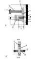
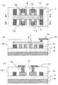
図1は単独の直方体状半導体層を有するシングル構造のMISFETを備えた半導体装置を表したものである。図1(a)はこの半導体装置の上面図、図1(b)は図1(a)のA−A’方向の断面図である。図1に示す形態ではシリコン基板5、埋め込み酸化膜4上に直方体状の半導体層38が形成され、この直方体状の半導体層38上にゲート絶縁膜7が設けられている。また、この半導体層38及びゲート絶縁膜7を跨ぐようにゲート電極6が設けられている。基板上のゲート電極22にはコンタクトホール13が設けられている。コンタクトホール13にはプラグが埋め込まれ、上部配線14と接続されている。この直方体状の半導体層38において、ゲート電極6の両側にソース/ドレイン領域が形成され、ゲート絶縁膜7下の部分(直方体状の半導体層38の上面及び側面)にチャネル領域が形成される。チャネル幅は直方体状半導体層38の高さHの2倍とその幅aとの合計に相当し、ゲート長はゲート電極6の幅dに相当する。 FIG. 1 shows a semiconductor device including a single-structure MISFET having a single rectangular semiconductor layer. FIG. 1A is a top view of the semiconductor device, and FIG. 1B is a cross-sectional view in the A-A ′ direction of FIG. In the form shown in FIG. 1, a rectangular
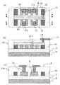
一方、特開2002−118255号公報には複数の直方体状半導体層を有するマルチ構造のMISFETが開示されている。図2(a)はこの半導体装置の上面図、図2(b)は図2(a)のA−A’方向の断面図である(図2では直方体状の半導体層が三つの場合を示す。)。この半導体装置では真ん中の半導体層29、一端の半導体層28及び半導体層28と反対側の半体層26が平行に配列され、これらの半導体層の中央部を跨いでゲート電極6が設けられている。また、一端の半導体層28には、ソース/ドレイン領域にコンタクトが形成されないか、形成されたとしてもチャネル領域に電流を流すトランジスタとして用いられない(図2は、半導体層28にソース/ドレイン領域とのコンタクトが設けられていない例を示す)。 On the other hand, Japanese Patent Laid-Open No. 2002-118255 discloses a multi-structure MISFET having a plurality of rectangular parallelepiped semiconductor layers. 2A is a top view of the semiconductor device, and FIG. 2B is a cross-sectional view taken along the line AA ′ of FIG. 2A (FIG. 2 shows a case where there are three rectangular semiconductor layers. .) In this semiconductor device, a
マルチ構造のフィン型のMISFETは従来、以下の方法によって製造されていた。図3及び4にこの製造方法の一例を示す。図3及び4は半導体層の幅方向(図2のA−A’方向断面に相当する)での断面図である。まず、貼り合わせ法又はSIMOX法によってシリコンウェハ基板5、SiO2酸化膜4及び単結晶シリコン膜2からなるSOI基板を用意する。次に、SOI基板の表面上に熱酸化法によってSiO2膜17を形成した後、不純物を単結晶シリコン膜2にイオン注入する(図3(a))。その後、エッチングによってSiO2膜17を除去する(図3(b))。続いて、単結晶シリコン膜2の全面にフォトレジスト9を塗布し、フォトリソグラフィーを用いて、所定パターンのレジストマスク9を形成する(図3(c))。次に、このレジストマスク9をエッチングマスクとして、単結晶シリコン膜2を異方性ドライエッチングした後、レジストマスク9を除去し、SiO2膜4上に所定高さの略直方体状の半導体層38を形成する(図3(d))。Conventionally, a multi-structure fin-type MISFET has been manufactured by the following method. 3 and 4 show an example of this manufacturing method. 3 and 4 are cross-sectional views in the width direction of the semiconductor layer (corresponding to the cross section in the AA ′ direction in FIG. 2). First, an SOI substrate composed of the
次に、熱酸化法やラジカル酸化法によって単結晶シリコンの略直方体状の半導体層38の表面に薄いゲート絶縁膜7を形成する。更に、このSiO2膜7上にCVD法によってポリシリコン膜19を形成し、不純物拡散で導電性とする。次いで、ポリシリコン膜19上にレジスト膜9を形成し、フォトリソグラフィーを用いてレジスト膜9を所定パターンに形成する(図4(a))。このレジスト膜9をマスクに用いてポリシリコン膜19に選択的エッチングを施し、ゲート電極6を形成する(図4(b))。Next, a thin gate
次に、エクステンションイオン注入を行った後、CVD法によりシリコン酸化膜等を堆積する。更に、堆積された絶縁物を異方性エッチングによってゲート電極6の側壁上に残す(図示していない)。これにより、略直方体状の半導体層38の側面及びゲート電極6の側壁上にそれぞれ絶縁膜が形成される。 Next, after extension ion implantation, a silicon oxide film or the like is deposited by a CVD method. Further, the deposited insulator is left on the sidewall of the
次に、このゲート電極6等をマスクとして不純物を略直方体状の半導体層38にドープし、ソース領域及びドレイン領域を形成する。 Next, an impurity is doped into the substantially
次に、上記構造上にCVD法を用いてSiO2などの層間絶縁膜16を形成した後、CMP法を用いて層間絶縁膜16を平坦化する。この後、フォトリソグラフィーとエッチングによってコンタクトホール13を形成する。コンタクトホール13はソース/ドレイン領域及びゲート電極6上に形成する。次に、タングステン膜、アルミニウム膜、TiN/Ti膜やそれらの積層膜をコンタクトホール13内に形成する。これによって、コンタクトプラグがコンタクトホール13内に形成される(図4(c))。この後、コンタクトプラグに電気的に接触する配線層14を形成する。配線層14はアルミニウムを主成分とした導電物から構成される。この後、これらの構造上にパッシベーション膜(図示していない)を形成する(図4(d))。Next, after an
また、特開2003−229575号公報にはあらかじめ基板全面に縞状パターンの凸状半導体領域を形成した後、必要な部分だけ残して残りの凸状半導体領域を除去することによって両端の半導体領域に対する近接効果の影響を防止し、エッチングの均一性を向上させた製造方法が開示されている。 Japanese Patent Laid-Open No. 2003-229575 discloses a method of forming a striped pattern of convex semiconductor regions on the entire surface of a substrate in advance and then removing the remaining convex semiconductor regions while leaving only necessary portions. A manufacturing method in which the influence of the proximity effect is prevented and the uniformity of etching is improved is disclosed.
しかしながら、従来のフィン型のMISFETの製造方法では、複数の半導体層形成時に両端の半導体層の形状、不純物濃度が他の半導体層と異なり、所望のトランジスタ特性を得られない場合があった。例えば、レジストマスクを用いて半導体層の形成を行う場合には、均一なエッチングを行えない場合があった。以下にその説明をする。 However, in the conventional method for manufacturing a fin-type MISFET, when a plurality of semiconductor layers are formed, the shape and impurity concentration of the semiconductor layers at both ends are different from those of other semiconductor layers, and desired transistor characteristics may not be obtained. For example, when the semiconductor layer is formed using a resist mask, uniform etching may not be performed. This will be described below.
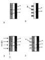
図5(a)は現像工程後にリンス液1によって洗浄した後の状態を表した図である(本例ではソース/ドレイン領域が共通化されていないマルチ構造のMISFETの製造工程を表している。)。図5(b)は図5(a)のA−A’方向の断面図である。この洗浄を行った後、レジストの間隙が小さいため、リンス液1がこの間隙に残留する。図5(c)はこの残留したリンス液1のレジストへの影響を表した図である。図5(d)は図5(c)のA−A’方向の断面図である。リンス液としては主に水が使用される。両端のレジスト15は一方の面しかリンス液1に接していないため、両端のレジスト15のうちリンス液1に接している面側は、リンス液の表面張力によって引っ張られ対向するレジスト側に変形してしまう(レジスト倒れ)。このため、後の工程でエッチングを行う際には、この両端のレジスト15に対応する両端の半導体層のエッチングを均一に行えない場合があった。 FIG. 5A is a diagram showing a state after the development process and after cleaning with the rinse solution 1 (in this example, a manufacturing process of a multi-structure MISFET in which the source / drain regions are not shared). ). FIG. 5B is a cross-sectional view in the A-A ′ direction of FIG. After this cleaning, since the resist gap is small, the
また、従来のフィン型のMISFETの製造方法では、エッチング時に両端の半導体層の幅が細くなってしまう場合があった。図6(a)はレジストパターンを形成した後、エッチングを行い半導体層を形成した状態を表した図である。図6(b)は図6(a)のA−A’方向の断面図である。また、図6(c)はソース/ドレイン領域が共通化されたMISFETについて同様にエッチングを行った後の半導体層を表している。図6では両端の半導体層18の幅(図6のa)がその他の半導体層の幅a’よりも細くなっている。これはマイクロローディング効果の非対称性によるものである。 Further, in the conventional method for manufacturing a fin-type MISFET, the width of the semiconductor layers at both ends may be narrowed during etching. FIG. 6A shows a state where a semiconductor layer is formed by etching after forming a resist pattern. FIG. 6B is a cross-sectional view in the A-A ′ direction of FIG. FIG. 6C shows the semiconductor layer after the MISFET having the common source / drain region is etched in the same manner. In FIG. 6, the width of the
このようにマイクロローディング効果が生じるのは、エッチング時に基板に入射するイオンが方向性を持っており、基板に対して垂直に入射するイオンだけでなく所定の角度を持って入射するイオンが存在するためである。このため、中央部の半導体層は、両端の半導体層に比べてエッチング速度が遅くなり、両端の半導体層は中央部の半導体層よりもより多くエッチングされる。このマイクロローディング効果はアスペクト比(開口部パターン幅に対するエッチング深さの比)が高いときにより顕著となる。 In this way, the microloading effect occurs because ions incident on the substrate during etching have directionality, and there are ions incident at a predetermined angle as well as ions incident perpendicularly to the substrate. Because. For this reason, the etching rate of the semiconductor layer at the center is slower than that of the semiconductor layers at both ends, and the semiconductor layers at both ends are etched more than the semiconductor layers at the center. This microloading effect becomes more prominent when the aspect ratio (ratio of etching depth to opening pattern width) is high.
このように従来の半導体装置の製造方法では、レジスト倒れやマイクロローディング効果に起因して均一なエッチングを行なえず、素子動作特性が不十分な場合があった。 As described above, in the conventional method for manufacturing a semiconductor device, uniform etching cannot be performed due to resist collapse or microloading effect, and element operating characteristics may be insufficient.
また、従来の製造方法ではゲート電極の加工性に劣る場合があった。図7(a)は、ゲート電極形成のため、複数の配列した半導体層38上にゲート絶縁膜7及びポリシリコン膜19を堆積しマスクとしてレジスト9を積層した後、レジスト9上に露光を行ったときの状態を表す上面図である。図7(b)は図7(a)のA−A’方向の断面図である。両端の半導体層18と基板との間に設けられたレジスト9には段差部20が生じている。 In addition, the conventional manufacturing method sometimes has poor gate electrode processability. In FIG. 7A, a
このレジスト9の露光時には、露光は半導体領域38の上面上のレジスト33にフォーカスが合うよう調節されている(図7(b)の35)。これに対して段差部20ではレジスト9の高さが徐々に減少しているため、露光がレジストに到達する際には広がってしまう(図7(b)の34:フォーカスオフセット)。この結果、段差部20のレジストは上面上のレジスト33に比べてより広い面積が露光され、段差部20のレジスト9の幅が細くなってしまう(サイズ異常の発生)。このレジスト9をマスクに用いてエッチングを行うと、該レジストのサイズ異常を反映して段差部20のポリシリコン膜19でもサイズ異常が発生し、半導体層38上に設けられたゲート電極6のゲート長d1よりも段差部20上のゲート電極6のゲート長d2の方が細くなってしまう。 When the resist 9 is exposed, the exposure is adjusted so that the resist 33 on the upper surface of the
更に、ゲート電極形成のためのエッチング時には段差部のゲート電極24には、上記フォーカスオフセットによる問題に加えてマイクロローディング効果によってゲート長異常が発生する場合があった。以下に説明する。図8(a)はゲート電極形成の為にエッチングを行った状態を表す図である。図8(b)は図8(a)のA−A’方向の断面図である。エッチング時に前述したマイクロローディング効果によって、半導体層18及び38間のポリシリコン膜36のエッチング速度は、段差部20のポリシリコン膜24のエッチング速度よりも遅くなってしまう。従って、段差部のポリシリコン膜24は、ポリシリコン膜36よりもより多くエッチングされる。このため、段差部20のゲート電極のゲート長d2は、半導体層18及び38上のゲート電極のゲート長d1よりも細くなってしまう(ゲート長異常の発生)。このように従来の製造方法ではゲート電極の加工性において問題が生じる場合があった。この場合、トランジスタ特性が安定化した半導体装置を製造することが困難であった。 Further, when etching for forming the gate electrode, the
また、図30は従来の半導体装置の製造方法におけるイオン注入工程を表した図である。図30(a)は上面図、図30(b)は図30(a)のB−B’方向の断面図である。図30に示されるように、ハローイオン注入やエクステンションイオン注入などは斜め方向から行う。この際、両側の半導体層18では片側側面に対向する位置に半導体層が設けられていないため、このイオン注入時の他の半導体領域からのイオンの跳ね返り量が少なくなる。これに対して、半導体層18で挟まれた半導体層38は両側に半導体層が設けられているため、イオン注入時のイオン跳ね返り量は多くなる。このように、斜め方向から行うイオン注入工程において、半導体層18と半導体層38とではイオン注入量が異なり、均一なトランジスタ特性を得ることが困難であった。 FIG. 30 is a diagram showing an ion implantation step in a conventional method for manufacturing a semiconductor device. 30A is a top view, and FIG. 30B is a cross-sectional view in the B-B ′ direction of FIG. 30A. As shown in FIG. 30, halo ion implantation, extension ion implantation, and the like are performed from an oblique direction. At this time, the
一般的に図1(b)で表されるように、ゲート電極とのコンタクトは基板上に設けられたゲート電極22上に設けられていた。このような構成の半導体装置では半導体層38の上面とゲート電極6との間には段差があるため、ソース/ドレイン領域とのコンタクトとゲートコンタクトを同時に形成する場合、ゲート電極とのコンタクトや配線形成の位置合わせには高度な技術が要求される場合があった。 In general, as shown in FIG. 1B, the contact with the gate electrode is provided on the
特開2002−118255号公報記載の半導体装置の製造方法では、チャネル領域が形成される半導体層と同程度の高さの一端の半導体層28(図2)を設け、この半導体層上にゲート電極6とのコンタクトが設けられている。この半導体装置の製造方法ではコンタクト、配線工程の安定化を図ることが可能であるが、反対側の半導体層26にはソース/ドレイン領域にコンタクトが形成され、トランジスタとして動作する。しかし、半導体層26については上記レジスト変形およびマイクロローディング効果の非対称性によってエッチングが均一に行われない場合があった。また、イオン注入が均一に行われなかったり、ゲート電極の加工性が劣るという問題があり、この半導体層26を用いて形成されたトランジスタを、半導体層29を用いて形成されたトランジスタと同様の特性をもつトランジスタとすることが困難な場合があった。 In the method for manufacturing a semiconductor device described in Japanese Patent Laid-Open No. 2002-118255, a semiconductor layer 28 (FIG. 2) at one end having the same height as a semiconductor layer in which a channel region is formed is provided, and a gate electrode is formed on the semiconductor layer. 6 is provided. In this method of manufacturing a semiconductor device, it is possible to stabilize the contact and wiring process. However, a contact is formed in the source / drain region in the
特開2003−229575号公報に記載の半導体装置の製造方法では不要な半導体領域を取り除くための工程を新たに設けなければならず、工程が複雑となる場合があった。また、特開2003−229575号公報に記載の半導体装置の製造方法では不要な半導体領域をゲート電極形成前に取り除くため、ゲート電極形成後の工程に関して、フォーカスオフセットの発生やマイクロローディング効果の非対称性を防止することができず、これらを原因とするゲート長異常が発生する場合があった。更に、ハローイオン注入やエクステンションイオン注入の均一性が劣化する場合があった。 In the method of manufacturing a semiconductor device described in Japanese Patent Laid-Open No. 2003-229575, a process for removing an unnecessary semiconductor region has to be newly provided, and the process may be complicated. In addition, in the semiconductor device manufacturing method described in Japanese Patent Application Laid-Open No. 2003-229575, unnecessary semiconductor regions are removed before forming the gate electrode. In some cases, gate length abnormalities may occur due to these problems. Furthermore, the uniformity of halo ion implantation or extension ion implantation may deteriorate.
本発明は上記課題に鑑みてなされたものであり、複数、設けられた半導体層のうち両端の半導体層で挟まれた半導体層については、チャネル領域に電流を流すトランジスタを備えた半導体装置を製造することによって、このチャネル領域が形成される半導体層のエッチングの均一性を向上させると共にゲート電極の加工性や平坦性、イオン注入の均一性を向上させることを目的とするものである。
また、素子動作特性及び信頼性に優れたMISFETを備えた半導体装置を得ることを目的とする。The present invention has been made in view of the above problems, and for a semiconductor layer sandwiched between semiconductor layers at both ends of a plurality of provided semiconductor layers, a semiconductor device including a transistor for supplying current to a channel region is manufactured. Thus, it is an object to improve the etching uniformity of the semiconductor layer in which the channel region is formed, and improve the workability and flatness of the gate electrode and the uniformity of ion implantation.
It is another object of the present invention to obtain a semiconductor device provided with a MISFET excellent in element operation characteristics and reliability.
上記課題を解決するため、本発明は以下の構成を有することを特徴とする。すなわち、本発明は第1の半導体領域と、第2の半導体領域とを備えた半導体装置であって、
(a)該第1の半導体領域は、基体から上方に突起した少なくとも1つの半導体層を有し、該半導体層を跨ぐように絶縁膜を介してゲート電極が設けられ、該半導体層の前記ゲート電極を挟んだ両側にソース/ドレイン領域が設けられて、
該半導体層の少なくとも両側面にチャネル領域が形成される電界効果型トランジスタが構成され、
(b)前記第2の半導体領域は、基体から上方に突起し、チャネル電流の方向と直交する方向において少なくとも第1の半導体領域を挟んだ両側に形成された半導体層を有し、該半導体層の第1の半導体領域側の側面は、該チャネル電流の方向と平行であることを特徴とする半導体装置に関する。In order to solve the above problems, the present invention is characterized by having the following configuration. That is, the present invention is a semiconductor device including a first semiconductor region and a second semiconductor region,
(A) The first semiconductor region has at least one semiconductor layer protruding upward from the base, and a gate electrode is provided through an insulating film so as to straddle the semiconductor layer, and the gate of the semiconductor layer Source / drain regions are provided on both sides of the electrode,
A field effect transistor having a channel region formed on at least both sides of the semiconductor layer;
(B) The second semiconductor region has a semiconductor layer that protrudes upward from the base and is formed on both sides sandwiching at least the first semiconductor region in a direction orthogonal to the direction of the channel current. The side surface on the first semiconductor region side is parallel to the direction of the channel current.
また、本発明は基体から上方に突起した少なくとも1つの半導体層を有する第1の半導体領域と、少なくとも前記第1の半導体領域を挟む両側に基体から上方に突起した半導体層を有する第2の半導体領域と、を形成するフィン型半導体層の形成工程と、
前記第1の半導体領域に含まれる半導体層を跨ぐようにゲート電極と、該ゲート電極と半導体層の少なくとも両側面の間に絶縁膜と、該半導体層のゲート電極を挟んだ両側にソース/ドレイン領域と、を形成するトランジスタの形成工程と、
を有することを特徴とする半導体装置の製造方法に関する。The present invention also provides a first semiconductor region having at least one semiconductor layer projecting upward from the base, and a second semiconductor having semiconductor layers projecting upward from the base on both sides sandwiching the first semiconductor region. A step of forming a fin-type semiconductor layer to form a region;
A gate electrode straddling the semiconductor layer included in the first semiconductor region, an insulating film between at least both side surfaces of the gate electrode and the semiconductor layer, and source / drain on both sides of the semiconductor layer with the gate electrode interposed therebetween A step of forming a transistor to form a region;
The present invention relates to a method for manufacturing a semiconductor device.
ここで、第1の半導体領域とはチャネル電流が流れ、基体上に複数、設けられた半導体層のうちチャネル電流の方向と直交する方向において、両端以外に設けられた半導体層を表す。また、第2の半導体領域とはチャネル電流が流れず、基体上に複数、設けられた半導体層のうちチャネル電流の方向と直交する方向において、両端と場合によっては両端以外に第1の半導体領域の間に設けられた半導体層を表す。 Here, the first semiconductor region refers to a semiconductor layer provided on both sides except for both ends in a direction orthogonal to the direction of the channel current among a plurality of semiconductor layers provided on the base body through which a channel current flows. In addition, the channel current does not flow with the second semiconductor region, and the first semiconductor region other than both ends and possibly both ends in the direction orthogonal to the direction of the channel current among the plurality of semiconductor layers provided on the
本発明では、複数、設けられた半導体層のうち、両端にチャネル電流が流れない半導体層(第2の半導体領域)を設けることによって、半導体層形成時に両端の半導体層で挟まれた半導体層の変形を防止し、高信頼性で素子特性に優れた半導体装置を製造することができる。例えば、半導体層形成をレジストマスクを用いたエッチングにより行う場合、両端のレジストマスクで挟まれたレジストマスクの倒れを効果的に防止するとともに、両端の半導体層で挟まれた半導体層のエッチング時のマイクロローディング効果の対称性を維持することができる。その結果、半導体層のエッチングが均一に行われ、素子特性に優れた半導体装置を得ることができる。 In the present invention, by providing a semiconductor layer (second semiconductor region) in which a channel current does not flow at both ends among a plurality of provided semiconductor layers, the semiconductor layers sandwiched between the semiconductor layers at both ends when the semiconductor layer is formed are provided. It is possible to manufacture a semiconductor device that prevents deformation, has high reliability, and has excellent element characteristics. For example, when the semiconductor layer is formed by etching using a resist mask, the resist mask sandwiched between the resist masks at both ends is effectively prevented from falling and the semiconductor layer sandwiched between the semiconductor layers at both ends is etched. The symmetry of the microloading effect can be maintained. As a result, the semiconductor layer is uniformly etched, and a semiconductor device having excellent element characteristics can be obtained.
本発明では、ゲート電極の加工性及び平坦性を向上させ、動作安定性に優れたトランジスタを備えた半導体装置を製造することができる。例えば、ゲート電極の形成を、レジストマスクを用いたエッチングによって行う場合には、第1の半導体領域に含まれる半導体層から両端の半導体層(第2の半導体領域)まで延在させてレジストマスクを形成することによって、レジストマスクの露光時に段差部に起因するフォーカスオフセットを防止すると共にマイクロローディング効果の対称性を維持することができる。 According to the present invention, it is possible to manufacture a semiconductor device including a transistor with improved workability and flatness of a gate electrode and excellent operational stability. For example, in the case where the gate electrode is formed by etching using a resist mask, the resist mask is extended from the semiconductor layer included in the first semiconductor region to the semiconductor layers at the both ends (second semiconductor regions). By forming the resist mask, it is possible to prevent a focus offset due to the step portion during exposure of the resist mask and to maintain the symmetry of the microloading effect.
本発明では、両端の半導体層で囲まれた半導体層については斜めイオン注入の環境を同一とできるため、斜めイオン注入の均一性を向上させ、動作安定性に優れたトランジスタを備えた半導体装置を製造することができる。
本発明では、第1の半導体領域に含まれる複数の半導体層にそれぞれ独立のソース/ドレイン領域及びゲート電極を設けることによって、集積密度が高い半導体装置を得ることができる。In the present invention, since the environment of oblique ion implantation can be made the same for the semiconductor layers surrounded by the semiconductor layers at both ends, a semiconductor device having a transistor with improved uniformity of oblique ion implantation and excellent operational stability is provided. Can be manufactured.
In the present invention, a semiconductor device having a high integration density can be obtained by providing independent source / drain regions and gate electrodes in a plurality of semiconductor layers included in the first semiconductor region.
本発明では、第1の半導体領域に含まれる複数の半導体層のうち、少なくとも2つの半導体層を跨ぐようにゲート電極を形成することによって、素子安定性及び設計自由度に優れた半導体装置とすることができる。
本発明では、基体上に更に、チャネル電流の方向と直交する方向に延在して、第1の半導体領域に含まれる複数の半導体層のうち、少なくとも2つの半導体層を挟んでソース/ドレイン領域を電気的に共通接続する連結半導体層を有することによって、ソース/ドレイン領域上へのコンタクトホールの位置合わせが容易となり、工程の簡素化を図ることができる。また、このようにソース/ドレイン領域の共通化を図ることによって、寄生抵抗の低減を図り、より少ない面積で大きなチャネル幅を実現でき、高集積化を図ることができる。In the present invention, a gate electrode is formed so as to straddle at least two semiconductor layers among a plurality of semiconductor layers included in the first semiconductor region, whereby a semiconductor device having excellent element stability and design flexibility is obtained. be able to.
In the present invention, the source / drain region further extends on the substrate in a direction perpendicular to the direction of the channel current and sandwiches at least two semiconductor layers among the plurality of semiconductor layers included in the first semiconductor region. By having the connecting semiconductor layer electrically connected in common, it is easy to align the contact hole on the source / drain region, and the process can be simplified. In addition, by sharing the source / drain regions in this manner, parasitic resistance can be reduced, a large channel width can be realized with a smaller area, and high integration can be achieved.
本発明では、第1の半導体領域に含まれる複数の半導体層の両側とその間に、第2の半導体領域に含まれる半導体層を設けることによって、ゲート電極同士が接触するのを防ぎ、動作特性に優れた半導体装置とすることができる。また、ゲート電極の平坦性を向上させることもできる。
本発明では、第1の半導体領域及び第2の半導体領域に含まれる半導体層の間隔を等しくすることによって、素子特性に優れた高信頼性の半導体装置とすることができる。In the present invention, by providing the semiconductor layers included in the second semiconductor region between both sides of the plurality of semiconductor layers included in the first semiconductor region, the gate electrodes are prevented from contacting each other, and the operating characteristics are improved. An excellent semiconductor device can be obtained. In addition, the flatness of the gate electrode can be improved.
In the present invention, a highly reliable semiconductor device having excellent element characteristics can be obtained by equalizing the distance between the semiconductor layers included in the first semiconductor region and the second semiconductor region.
本発明では、ゲート電極が、第1の半導体領域に含まれる半導体層上から、第2の半導体領域に含まれる半導体層上まで延在して設け、第2の半導体領域上にゲート電極とのコンタクトを形成することによって、安定したコンタクトが可能であり、素子特性に優れた半導体装置とすることができる。また、ゲート電極の平坦性を向上させることができる。 In the present invention, the gate electrode is provided so as to extend from the semiconductor layer included in the first semiconductor region to the semiconductor layer included in the second semiconductor region, and the gate electrode is formed on the second semiconductor region. By forming the contact, a stable contact is possible, and a semiconductor device having excellent element characteristics can be obtained. In addition, the flatness of the gate electrode can be improved.
本発明では、第1の半導体領域に含まれる半導体層を、略直方体状とすることによって、動作特性及び素子安定性に優れた半導体装置を得ることができる。
本発明では、第2の半導体領域に含まれる半導体層の長さを、ゲート長以上とすることによって、マイクロローディング効果の対称性が保たれ、所望形状の加工が可能となり、動作安定性及び素子特性に優れた半導体装置とすることができる。In the present invention, a semiconductor device excellent in operating characteristics and element stability can be obtained by forming the semiconductor layer included in the first semiconductor region into a substantially rectangular parallelepiped shape.
In the present invention, by setting the length of the semiconductor layer included in the second semiconductor region to be equal to or longer than the gate length, the symmetry of the microloading effect is maintained, processing of a desired shape is possible, operation stability and element A semiconductor device having excellent characteristics can be obtained.
本発明では、第1の半導体領域に含まれる半導体層のソース/ドレイン領域の幅を太くすることによって、コンタクトの位置合わせが容易であり、動作安定性に優れた半導体装置とすることができる。また、寄生抵抗の低減を図ることもできる。 In the present invention, by increasing the width of the source / drain region of the semiconductor layer included in the first semiconductor region, contact alignment is easy, and a semiconductor device having excellent operational stability can be obtained. In addition, parasitic resistance can be reduced.
(半導体装置)
本発明の半導体装置は、第1の半導体領域と、チャネル電流の方向と直交する方向において、第1の半導体領域の両側に第2の半導体領域を有し、第1の半導体領域に含まれる半導体層の少なくとも側面にチャネル領域が形成されることを特徴とする。(Semiconductor device)
The semiconductor device of the present invention includes a first semiconductor region and a semiconductor included in the first semiconductor region, the second semiconductor region on both sides of the first semiconductor region in a direction orthogonal to the channel current direction. A channel region is formed on at least a side surface of the layer.
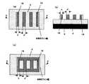
図9は本発明の半導体装置の一例を示したものである。図9(a)は第1の半導体領域として複数の半導体層8を有する半導体装置の上面図である。また、図9(b)は図9(a)のA−A’方向の断面図、図9(c)は図9(a)のB−B’方向の断面図、図9(d)は図9(a)のC−C’方向の断面図である(図9(a)では層間絶縁膜16及び配線14を図中に示していない。また、図9(a)〜(c)ではゲートサイドウォール44を図中に示していない。)。 FIG. 9 shows an example of a semiconductor device of the present invention. FIG. 9A is a top view of a semiconductor device having a plurality of
この半導体装置はSOI基板を用いて形成されたものであり、シリコン基板5上に埋め込み絶縁膜4が設けられ、埋め込み絶縁膜4上に突出した第1の半導体領域に含まれる半導体層8及び第2の半導体領域に含まれる半導体層10が形成されている。ここで、半導体層8のソース/ドレイン領域上にはコンタクトが形成されており、チャネル領域に電流を流すトランジスタとして動作するが、半導体層10にはチャネル電流が流れない。半導体層10にチャネル電流を流さない方法としては、半導体層10のソース/ドレイン領域のうち少なくとも一方にコンタクトを形成しない場合や、ソース/ドレイン領域上にコンタクトを形成しても配線を電気的に接続しない場合、ソース/ドレイン領域に電気的に接続した配線を接地したり、同電位の電源に接続する場合などが挙げられる。 This semiconductor device is formed using an SOI substrate. A buried insulating
また、複数の半導体層(半導体層8及び10)の配列において、第2の半導体領域は少なくとも1つ以上の半導体層(第1の半導体領域に含まれる半導体層8)を両側から挟むように形成されている。 In the arrangement of the plurality of semiconductor layers (semiconductor layers 8 and 10), the second semiconductor region is formed so as to sandwich at least one semiconductor layer (
なお、半導体層8の数は少なくとも1つ以上であれば良く、その数は特に限定されるわけではない。また、複数の半導体層8を設ける場合、各半導体層8を流れるチャネル電流の方向が互いに平行となるように配列することが好ましい。ここで、チャネル領域は半導体層8の上面及び側面に形成され、チャネル電流は、図9(a)の46及び図9(d)で表されるように半導体層に形成されたドレイン領域45−ソース領域43間を流れる。ソース/ドレイン領域は、半導体層8のうちゲート電極に覆われていない部分に形成するため、このチャネル電流の方向は、ゲート電極が延在して設けられた方向に垂直である。また、基板と平行な方向であり、半導体層8及び10の配列方向に垂直である。 The number of
また、半導体層8は主たるチャネル領域が形成される側面を有する。ここで側面とは、基体から突起した半導体層8のうち基体と略平行でない部分を表し、側面の形状としては例えば、曲面状、湾曲状、基体と垂直な面、テーパー状などを挙げることができる。また、これらの形状が複数種、組み合わさった形状であっても良い。側面が湾曲状、テーパー状の場合、湾曲の度合いやテーパーの角度は所望の形状とすることができる。半導体層8の両側面は対称であっても非対称であっても良い。 The
チャネル電流の方向と直交する方向47において、半導体層8(第1の半導体領域)の両側には、第2の半導体領域が形成されている。第2の半導体領域は基体上に突起した半導体層10からなり、図9では第1の半導体領域の両側にそれぞれ1つずつ半導体層10が設けられている。両側の半導体層10の数は1つ以上であれば良く、その数は特に限定されるわけではない。 In a direction 47 orthogonal to the direction of the channel current, second semiconductor regions are formed on both sides of the semiconductor layer 8 (first semiconductor region). The second semiconductor region is composed of a
両側の半導体層10は同一形状である必要はなく、異なる形状を有していても良いが、半導体層10の第1の半導体領域側の側面(第1の半導体領域に対向する側面)48はチャネル電流の方向46(図9(a)では一例として矢印46の向きにチャネル電流が流れる場合を示している。配線の配置によってはチャネル電流の向きが矢印46と逆向きであっても良い)と平行になっている必要がある。側面48が平行になっていることにより、加工性に優れ、所望形状の半導体装置とすることができる。側面48の形状は平行であれば特に限定されるわけではなく、例えば、半導体層8の側面と同様の形状とすることができる。また、半導体層8の形成時に半導体層10が悪影響を及ぼすことがない。なお、第2の半導体領域に含まれる半導体層のうち側面48と反対側の側面の形状は、特に限定されるわけではなくテーパー状、曲面状、基体から垂直な形状であっても良い。なお、半導体層10にはソース/ドレイン領域が形成されていても良いし、されていなくても良い。 The semiconductor layers 10 on both sides do not need to have the same shape, and may have different shapes, but the side surface (side surface facing the first semiconductor region) 48 of the
半導体層8の間の間隔aは等しいことが好ましい。また、第1の半導体領域の両側に設けられた半導体層10のうち、一方の半導体層10とこれに対向する半導体層8の間隔は、他方の半導体層10とこれに対向する半導体層8の間隔に等しいことが好ましい。より好ましくは、全ての半導体層(半導体層8及び10)間の間隔が等しいのが良い。このように半導体層間の間隔が等しいことによって、ソース/ドレイン領域形成のためのイオン注入やエッチングなどの処理を均一に行うことができ、素子特性に優れた高信頼性の半導体装置とすることができる。 The distance a between the semiconductor layers 8 is preferably equal. Of the semiconductor layers 10 provided on both sides of the first semiconductor region, the distance between one
図9ではゲート電極6は、一方の半導体層10から他方の半導体層10まで延在して電気的に共通接続されている。ゲート電極6と各半導体層8との間にはゲート絶縁膜7が形成されている。なお、ゲート電極6は半導体層8の少なくとも1つを跨ぐように形成されていれば良く、その数は限定されるわけではない。 In FIG. 9, the
更にゲート電極6は図9のように第1の半導体領域に含まれる半導体層8だけでなく、半導体層8から第2の半導体領域に含まれる半導体層10まで延在して形成されていても良い。この際、ゲート電極6は半導体層10上面の少なくとも一部まで延在して形成されていれば良く、半導体層10の全てを跨ぐように形成されていなくても良い。このように半導体層10の上面までゲート電極6が設けられている場合、第一の半導体領域に含まれる半導体層8のうち、一番端に位置する半導体層8の両側の上方においてゲート電極6が対称性の高い構造となる。すなわち、ゲート電極が半導体層8の左右両側の上方において、ともに隣接する半導体層8または10まで延在する構造となる。このため、例えば、レジストマスクを用いたエッチングによってゲート電極を形成する場合、半導体層8上方のゲート電極ではフォーカスオフセットやマイクロローディング効果の非対称性がより低減される。また、斜めイオン注入に関する非対称性も低減され、素子特性に優れた半導体装置とすることができる。 Furthermore, the
また、図9(d)に示されるように半導体層8のゲート電極6が設けられていない部分には、それぞれソース領域43およびドレイン領域45が設けられている。ゲート電極6直下の半導体層8の上面及び側面にはチャネル領域が形成され、この半導体装置はいわゆるトリプルゲート型のフィン型のトランジスタとなる。ゲート電極6に電圧が印加されるとソース領域43−ドレイン領域45間をチャネル電流が流れる。 Further, as shown in FIG. 9D, a
図9(b)及び(c)に示されるように各半導体層8のソース/ドレイン領域は共通のコンタクトを通して上方に設けられた配線14と接続されている。また、ゲート電極とのコンタクトは一方の半導体層10の上方で行われている。ゲート電極とのコンタクトの位置は特に限定されるわけではないが、好ましくは半導体層10の上方に設けるのが良い。このように半導体層10の上方でのコンタクトは、位置合わせが容易であり、安定したコンタクトを取ることが可能なため素子特性に優れた半導体装置とすることができる。また、コンタクト以外の部分には層間絶縁膜16が設けられている。 As shown in FIGS. 9B and 9C, the source / drain regions of each
図10は本発明の半導体装置の他の一例を示したものである。図10の半導体装置では、第1及び第2の半導体領域に含まれる半導体層8及び10がシリコン基板2から直接、突出して形成されている点に特徴がある。図10(a)はこの半導体装置の上面図、図10(b)は図10(a)のA−A’方向の断面図、図10(c)は図10(a)のB−B’方向の断面図である。また、突起した半導体層8及び10以外の部分には分離絶縁膜42が形成されている。 FIG. 10 shows another example of the semiconductor device of the present invention. The semiconductor device of FIG. 10 is characterized in that the semiconductor layers 8 and 10 included in the first and second semiconductor regions are formed so as to protrude directly from the
図11は図9の半導体装置の変形例を示したものである。図11(a)はこの半導体装置の上面図、図11(b)は図11(a)のA−A’方向の断面図、図11(c)は図11(a)のB−B’方向の断面図である。図11の半導体装置では第1の半導体領域に含まれる半導体層8の上面上に形成されるゲート絶縁膜7が、図9の半導体装置よりも厚くなっている。このため、この半導体装置は半導体層8の上面にはチャネル領域が形成されず、側面にのみチャネル領域が形成される、いわゆるダブルゲート型のトランジスタとなる。また、ゲート電極は一方の半導体層10から他方の半導体層10の上面の一部まで延在して設けられている。 FIG. 11 shows a modification of the semiconductor device of FIG. 11A is a top view of the semiconductor device, FIG. 11B is a cross-sectional view taken along the line AA ′ of FIG. 11A, and FIG. 11C is BB ′ of FIG. It is sectional drawing of a direction. In the semiconductor device of FIG. 11, the
図12は、図9の半導体装置の変形例を示したものである。図12(a)はこの半導体装置の上面図、図12(b)は図12(a)のA−A’方向の断面図、図12(c)は図12(a)のB−B’方向の断面図である。この半導体装置では、第1の半導体領域に含まれる半導体層8が四つ配列されており、そのうちの二つの半導体層8(左側の二つ)上にはそれぞれ独立したゲート電極6が設けられている。また、残りの二つの半導体層8(右側の二つ)については、この二つの半導体層8を跨ぐように電気的に共通接続されたゲート電極6が設けられている。なお、第2の半導体領域に含まれる半導体層10上にはゲート電極6は形成されていない。 FIG. 12 shows a modification of the semiconductor device of FIG. 12A is a top view of the semiconductor device, FIG. 12B is a cross-sectional view in the direction of AA ′ of FIG. 12A, and FIG. 12C is BB ′ of FIG. It is sectional drawing of a direction. In this semiconductor device, four
各半導体層8のソース領域とドレイン領域はそれぞれ独立したコンタクトによって個別の配線14に接続されている。なお、各ゲート電極6とのコンタクトは、半導体層8の上方で設けられている。右側の二つの半導体層8を跨ぐように共通化されたゲート電極6については、最も右側の半導体層8上方でゲート電極6とのコンタクトが設けられている。これらのゲート電極6はそれぞれ個別の配線に接続されていても良いし、共通の配線に接続されていても良い。 The source region and the drain region of each
このように本発明の半導体装置では、半導体装置内に各半導体層8上にそれぞれ独立して設けたゲート電極と、複数の半導体層8を跨ぐように共通化されたゲート電極とを混在させて設けることができる。このため、素子安定性及び装置の設計自由度に優れた半導体装置とすることができる。 Thus, in the semiconductor device of the present invention, the gate electrode provided independently on each
図13は、図12の半導体装置の変形例を示したものである。図13(a)は半導体装置の上面図、図13(b)は図13(a)のA−A’方向の断面図、図13(c)は図13(a)のB−B’方向の断面図である。図13の半導体装置では図12の半導体装置と異なり、ゲート電極6が第2の半導体領域に含まれる一方の半導体層10から他方の半導体層10まで延在して設けられており、ゲート電極が共通化されている。このように、回路の構成上必要とされる場合には、ゲート電極を共通化することができる。 FIG. 13 shows a modification of the semiconductor device of FIG. 13A is a top view of the semiconductor device, FIG. 13B is a cross-sectional view in the AA ′ direction of FIG. 13A, and FIG. 13C is a BB ′ direction in FIG. 13A. FIG. In the semiconductor device of FIG. 13, unlike the semiconductor device of FIG. 12, the
また、図13(a)に示すように、各半導体層8のうち左側の二つにおいては、図示されたソース/ドレイン領域のうち、上側に図示されたソース領域又はドレイン領域が、二つの半導体層8で共通のコンタクトが形成されているが、それ以外のソース/ドレイン領域においてはそれぞれ独立にコンタクトが形成されている。このように複数のソース/ドレイン領域とのコンタクトのうち、一部は共通のコンタクトとし、残りは独立のコンタクトであるようにしても良い。また、図13(c)に示すように、各半導体層8のうち下側のソース/ドレイン領域はそれぞれ独立のコンタクトが設けられているが、左側二つについては共通の配線に接続されている。このように独立なコンタクトどうしを適宜配線によって接続しても良い。なお、複数の半導体層8が配列されている場合、一部の半導体層8に対してはそれぞれ個別のゲート電極6が設けられ、残りの半導体層8に対しては共通したゲート電極が設けられていても良い。 As shown in FIG. 13A, in the left two of the semiconductor layers 8, the source or drain region shown on the upper side of the source / drain regions shown in the drawing is two semiconductors. Although a common contact is formed in the
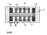
図14は、本発明の半導体装置の他の一例を示したものである。この半導体装置は第2の半導体領域に含まれる半導体層10が、第1の半導体領域の両側だけでなく、第1の半導体領域に含まれる半導体層8の間にも設けられている点に特徴がある。図14(a)は、この半導体装置の上面図、図14(b)は図14(a)のA−A’方向の断面図、図14(c)は図14(a)のB−B’方向の断面図である。図14では複数の配列された半導体層8の両側と真ん中にそれぞれ1つの半導体層10が設けられている。なお、半導体層8の間に設ける半導体層10の数は特に限定されるわけではなく二つ以上であっても良い。また、半導体層8間の位置のうち複数の異なる位置に半導体層10を設けても良いし、同じ位置に二つ以上の半導体層10を設けても良い。例えば、チャネル電流の方向と直交する方向に半導体層8と半導体層10がそれぞれ交互に配列されるように設けても良い。ただし、半導体層8の間に設ける半導体層10の側面は、半導体層8のチャネル電流の方向と平行になっている必要がある。半導体層8の間に設ける半導体層10の形状は特に限定されるわけではないが、好ましくは半導体層8と同一形状かつ平行であるのが良い。 FIG. 14 shows another example of the semiconductor device of the present invention. This semiconductor device is characterized in that the
図14では、ゲート電極6は二つ設けられており、各ゲート電極6は両側の半導体層10のうち一方の半導体層10から二つの半導体層8を跨ぐように設けられている。本半導体装置では、ゲート電極6が真ん中の半導体層10まで延在して設けられていないため、複数のゲート電極を設ける場合に、ゲート電極同士を電気的に接触するのを防ぎ、動作特性に優れた半導体装置とすることができる。なお、ゲート電極は真ん中の半導体層10まで延在して設けても良い。この場合、半導体層8から見たゲート電極の構造対称性を高めることができる。 In FIG. 14, two
ゲート電極とのコンタクトはそれぞれ両側の半導体層10の上方で設けられているが、コンタクトは真ん中の半導体層10の上方に設けても良い。
図15は図9の半導体装置の変形例を示したものである。図15(a)は半導体装置の上面図、図15(b)は図15(a)のA−A’方向の断面図、図15(c)は図15(a)のB−B’方向の断面図である。この半導体装置は、第1の半導体領域に含まれる各半導体層8について、ソース/ドレイン領域の幅(チャネル電流の方向と直交する方向の長さ)aがゲート電極に覆われた半導体層の部分の幅a’よりも大きい点に特徴がある。このようにソース/ドレイン領域の幅が太いことによってコンタクトの位置合わせが容易となり、動作安定性に優れた半導体装置とすることができる。また、寄生抵抗の低減を図ることもできる。Although the contact with the gate electrode is provided above the
FIG. 15 shows a modification of the semiconductor device of FIG. 15A is a top view of the semiconductor device, FIG. 15B is a cross-sectional view in the AA ′ direction of FIG. 15A, and FIG. 15C is a BB ′ direction in FIG. 15A. FIG. In this semiconductor device, for each
半導体層8のうちゲート電極に覆われた部分と、ソース/ドレイン領域の部分の形状は特に限定されるわけではない。例えば、側面が曲面状のものやテーパー形状のもの等を挙げることができる。好ましくは、ゲート電極に覆われた部分と、ソース/ドレイン領域の部分の形状は略直方体状であることが好ましい。略直方体状であることによって、プロセスの対称性が増し、安定した素子特性をもつ半導体装置とすることができる。また、半導体層8のソース領域とドレイン領域の形状は対称である必要はなく、互いに異なる形状であっても良い。半導体層8のソース領域、およびドレイン領域の部分の幅は、ゲート電極に覆われた部分の幅の1.1〜10倍であることが好ましく、2〜5倍であることがより好ましい。 The shape of the portion of the
図16は本発明の半導体装置の他の一例を示したものである。図16(a)はこの半導体装置の上面図、図16(b)は図16(a)のA−A’方向の断面図、図16(c)は図16(a)のB−B’方向の断面図である。この半導体装置は、第1の半導体領域に含まれる半導体層8が4つ存在し、その中の2つの半導体層8がチャネル電流の方向と直交する方向に延在した半導体層32(図16(a)の点線で囲まれた部分)によって連結されており、二つの半導体層8のソース/ドレイン領域が共通化されている点に特徴がある。この二つの半導体層8は、マルチフィン型のトランジスタを構成する。このような半導体装置は、コンタクトの位置合わせが容易であり、寄生抵抗の低減を図ることができる。また、より少ない面積で大きなチャネル幅を実現でき、高集積化を図ることができる。 FIG. 16 shows another example of the semiconductor device of the present invention. 16A is a top view of the semiconductor device, FIG. 16B is a cross-sectional view taken along the line AA ′ of FIG. 16A, and FIG. 16C is BB ′ of FIG. It is sectional drawing of a direction. In this semiconductor device, there are four
図16の半導体装置では、ソース/ドレイン領域とのコンタクトは、ソース/ドレイン領域の一部上に設けられているが、コンタクトの位置は図16の位置に限定されるわけではなく、ソース/ドレイン領域上の何れか一部の上であれば良い。 In the semiconductor device of FIG. 16, the contact with the source / drain region is provided on a part of the source / drain region, but the position of the contact is not limited to the position of FIG. It may be on any part of the region.
また、図16ではゲート電極6は一方の第2の半導体領域に含まれる半導体層10から他方の半導体層10まで全ての半導体層を跨ぐように延在して形成されているが、両端の半導体層10上まで延在して形成されていなくても良い。更に、複数の半導体層8が配列された場合、一部の半導体層8についてはソース領域、およびドレイン領域がそれぞれ独立して設けられ、残りの半導体層8については図16のようにソース領域、およびドレイン領域が共通化されていても良い。 In FIG. 16, the
図17は図16の半導体装置の変形例を示したものである。図17(a)は半導体装置の上面図、図17(b)は図17(a)のA−A’方向の断面図、図17(c)は図17(a)のB−B’方向の断面図である。図17の半導体装置では、第1の半導体領域のソース/ドレイン領域が、チャネル電流の方向に関して対称となっていない点に特徴がある。例えば、図17では、一方の領域は四つの半導体層8が共通化されて形成されており、他方の領域は二つの半導体層8が共通化されている。ソース/ドレイン領域が共通化される半導体層8の数は2つ以上であれば良く、その数は特に限定されるわけではない。 FIG. 17 shows a modification of the semiconductor device of FIG. 17A is a top view of the semiconductor device, FIG. 17B is a cross-sectional view in the AA ′ direction of FIG. 17A, and FIG. 17C is a BB ′ direction in FIG. 17A. FIG. The semiconductor device of FIG. 17 is characterized in that the source / drain regions of the first semiconductor region are not symmetric with respect to the direction of the channel current. For example, in FIG. 17, one region is formed by sharing four
図18は図9の半導体装置の変形例を示したものである。図18はこの半導体装置の上面図である。図18の半導体装置では第1の半導体領域に含まれる半導体層8の数が1つであり、その両側に第2の半導体領域が設けられている。この半導体装置はシングルフィン型のトランジスタを構成する。例えば、同一基板上にこのようなトランジスタと複数の半導体層8を持つトランジスタを設ける場合、これらの半導体装置の半導体層8のマイクロローディング効果等のエッチング状態を同じにでき、寸法精度を一定にすることができる。また、斜めイオン注入の均一性を高めることができる。 FIG. 18 shows a modification of the semiconductor device of FIG. FIG. 18 is a top view of the semiconductor device. In the semiconductor device of FIG. 18, the number of the semiconductor layers 8 included in the first semiconductor region is one, and the second semiconductor regions are provided on both sides thereof. This semiconductor device constitutes a single fin type transistor. For example, when such a transistor and a transistor having a plurality of
図19は本発明の半導体装置の他の一例を示したものである。図19はこの半導体装置の上面図である。図19の半導体装置では、第2の半導体領域に含まれる半導体層10のチャネル電流の方向の長さAは、第1の半導体領域に含まれる半導体層8の長さよりは短いが、ゲート長Bよりも長くなっている。このように半導体層10の長さが少なくともゲート長以上であることによって、半導体層形成時に半導体層8のチャネル領域となる部分のエッチング時におけるマイクロローディング効果の対称性が保たれ、所望形状に加工することができる。このため、動作安定性及び素子特性に優れた半導体装置とすることができる。 FIG. 19 shows another example of the semiconductor device of the present invention. FIG. 19 is a top view of the semiconductor device. In the semiconductor device of FIG. 19, the length A in the direction of the channel current of the
図20は図19の半導体装置の変形例を示したものである。図20はこの半導体装置の上面図である。図20の半導体装置では、半導体層10のチャネル電流の方向の長さAが半導体層8の長さBよりも長い点に特徴がある。このように半導体層10の長さが半導体層8の長さ以上であることによって、半導体層形成時に半導体層8の側面を均一に所望形状に加工することができる。このため、動作安定性及び素子特性に優れた半導体装置とすることができる。 FIG. 20 shows a modification of the semiconductor device of FIG. FIG. 20 is a top view of the semiconductor device. The semiconductor device of FIG. 20 is characterized in that the length A of the
図21は本発明の半導体装置の他の一例を示したものである。図21はこの半導体装置の上面図である。この半導体装置は、半導体層10のチャネル電流の方向と直交する方向の幅Aが半導体層8の幅Bよりも太い点に特徴がある。このように半導体層10の幅Aが半導体層8の幅Bよりも太いことによって、半導体層10の上方でのコンタクトの位置合わせが容易となり、寄生抵抗を小さくすることが出来る。また、半導体層10の機械的強度が大きくなるため、半導体層形成時にレジストマスクを用いた場合に、より効果的にレジスト倒れを防止することができる。また、半導体層8を所望形状に加工することと高集積化の観点から、半導体装置の最適化を図ることができる。 FIG. 21 shows another example of the semiconductor device of the present invention. FIG. 21 is a top view of the semiconductor device. This semiconductor device is characterized in that the width A of the
図31は、本発明の半導体装置が複数、基板上に設けられた一例を表すものである(上面図)。図31では、チャネル電流の方向に三つの半導体装置50〜52が設けられている。半導体装置50は図11の半導体装置に、半導体装置51は図14の半導体装置に相当する。これらの半導体装置はn型のMISFETであっても、p型のMISFETであっても良い。また、これらのMISFETが混在するものであっても良い。 FIG. 31 illustrates an example in which a plurality of semiconductor devices of the present invention are provided over a substrate (top view). In FIG. 31, three
各半導体装置の第1の半導体領域に含まれる各半導体層8は、チャネル電流と直交する方向の中心53が一致するように互いに等間隔に配列されている。このように中心53が一致するように半導体層8を設けることによって、素子特性に優れ、集積密度の高い半導体装置とすることが可能となる。また、第2の半導体領域に含まれる半導体層54は全ての半導体層8を両側から挟むように、三つの半導体装置で共通化して設けられている。このように両側の半導体層54を共通化して設けることにより、半導体層の形成工程が容易となり、素子密度が高く設計精度に優れた半導体装置とすることができる。なお、各半導体装置間で、半導体層8は中心53が一致するように設けられていなくても良く、また、半導体層8の間隔が異なっていても良い。半導体層54は、それぞれの半導体装置で個別に設けられていても良いが、チャネル電流と直交する方向の中心が互いに一致するように配列されることが好ましい。 Each
半導体装置51及び52は更に、半導体層54の間に第2の半導体領域に含まれる半導体層10が設けられている(半導体装置51では半導体層8の間に1つの半導体層10が、半導体装置52では半導体層54と半導体層8の間に2つの半導体層10が設けられている)。このように半導体層8の設けられていない部分に半導体層10を設けることによって、半導体層形成時に各半導体層8を均一に形成することができる。なお、半導体層54の間に設ける半導体層10は、他の半導体装置に含まれる半導体層8又は10と中心53が一致するように設けることが好ましい。 In the
図22は本発明の半導体装置の他の一例を示したものである。図22の半導体装置では、第1の半導体領域の両側に設けられた半導体層10が、一方の半導体層10から他方の半導体層10まで半導体層8を囲むように一対の半導体層49(点線で囲まれた部分)が更に形成されている。この半導体装置では半導体層10及び49が第2の半導体領域を構成する。また、この半導体装置では、半導体層8が半導体層10及び49によって囲まれているため、半導体層形成時に半導体層8の全ての部分のプロセスの対称性を保つことができる。このため、素子安定性及び高駆動特性を有する半導体装置とすることができる。また、ゲート電極6はチャネル電流と直交する方向に、一方の半導体層10から他方の半導体層10まで延在して設けられている。ゲート電極6とのコンタクトは半導体層10の一部の上方に設けられている。 FIG. 22 shows another example of the semiconductor device of the present invention. In the semiconductor device of FIG. 22, a pair of semiconductor layers 49 (indicated by dotted lines) so that the semiconductor layers 10 provided on both sides of the first semiconductor region surround the
(半導体装置の製造方法)
以下に本発明の製造方法を説明する。
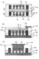
図23は本発明の製造方法の一例として、第1の半導体領域に含まれる複数の半導体層8のソース/ドレイン領域がそれぞれ共通のコンタクトを通して配線14に接続された半導体装置の製造方法を表したものである。(Method for manufacturing semiconductor device)
The production method of the present invention will be described below.
FIG. 23 shows a method for manufacturing a semiconductor device in which source / drain regions of a plurality of
まず、基体上に突起した第1の半導体領域と、第1の半導体領域の両側に、基体上に突起した第2の半導体領域を形成する。この第1及び第2の半導体領域は、基体上に設けられた半導体基板を所定形状に加工することで形成することができる。一例として所定形状のマスクを用いてSOI基板にエッチングを行うことにより、半導体層を形成する方法を説明する。マスクとしては、レジストマスク、SiO2膜などを用いることができる。First, a first semiconductor region projecting on the base and a second semiconductor region projecting on the base are formed on both sides of the first semiconductor region. The first and second semiconductor regions can be formed by processing a semiconductor substrate provided on the base body into a predetermined shape. As an example, a method for forming a semiconductor layer by etching an SOI substrate using a mask having a predetermined shape will be described. As the mask, a resist mask, a SiO2 film, or the like can be used.
まず、SOI基板を用意し、所定方向に配列された複数のマスク3とマスク3の両側にマスク25を設ける。マスクとしては例えば、レジストマスクを使用することができる。図23(a)はこの状態を表したものである。図23(b)は図23(a)のA−A’方向の断面図である。図23では一例として六つのマスクからなるマスクパターンが示されている。 First, an SOI substrate is prepared, and a plurality of
マスクの形状は後に形成する半導体層の形状に合わせて、所望の形状とすることができる。好ましくは、図23に示されるように略直方体状であるのが良い。このように第1の半導体領域に含まれる半導体層に対応するマスクを挟んだ両側に、第2の半導体領域に含まれる半導体層に対応するマスクを設けることによって、第1の半導体領域に含まれる半導体層に対応するマスクの倒れを防止し、後工程でのエッチングを均一に行うことができる。 The shape of the mask can be a desired shape in accordance with the shape of a semiconductor layer to be formed later. Preferably, it is good to have a substantially rectangular parallelepiped shape as shown in FIG. Thus, by providing the mask corresponding to the semiconductor layer included in the second semiconductor region on both sides of the mask corresponding to the semiconductor layer included in the first semiconductor region, the mask is included in the first semiconductor region. The mask corresponding to the semiconductor layer can be prevented from falling down, and etching in the subsequent process can be performed uniformly.
図23に示されるように第2の半導体領域に含まれる半導体層10が第1の半導体領域の両側にある場合には、この半導体層10に対応するマスク25の幅(マスクの配列方向の長さ:図中のa)は、マスクの変形防止の観点から、マスク3の幅a’よりも太い方が好ましい。また、半導体層10が、更に第1の半導体領域に含まれる半導体層8の間にある場合には、この半導体層10に対応するマスクの幅はプロセスの対称性の観点から、マスク3の幅a’と等しい方が好ましいが、回路レイアウトの要請がある場合には太くしても良い。 As shown in FIG. 23, when the
マスク25の長手方向長さ(マスクの配列方向と直交する方向の長さ:図中のL)は、後の工程で形成されるゲート電極6のゲート長(図24(c)のd)以上が好ましい。より好ましくは、マスク25の長さLは、マスク3の長さL’以上にするのが良い。マスク25の幅や長さをこのようにすることによって、マスク25の機械的強度を高くして、マスク形成時により効果的にマスク3の損傷を防止することができる。例えば、マスクとしてレジストマスクを使用した場合、フォトリソグラフィー工程後の洗浄時にリンス液によるマスクの倒れを防止し、後の工程でエッチングをより均一に行うことができる。なお、図23ではマスク25の幅がマスク3の幅よりも太く、マスク25の長さLが、マスク3の長さL’と等しい場合を示している。 The length in the longitudinal direction of the mask 25 (the length in the direction orthogonal to the arrangement direction of the mask: L in the figure) is equal to or longer than the gate length of the gate electrode 6 (d in FIG. 24C) formed in a later step. Is preferred. More preferably, the length L of the
マスク25の長さは、マスク3の長さ以上であることが好ましい。マスク25の長さがこれらの範囲内にあることによって、マスク形成時のマスク3の損傷をより効果的に防止することができる。例えば、マスクがレジストマスクである場合、レジスト倒れを効果的に防止することができる。また、エッチング時の半導体層8におけるマイクロローディング効果の対称性を保ち、所望形状の半導体層8を得ることができる。 The length of the
マスク3の間の間隔cは一定であることが好ましい。また、一方のマスク25とその隣のマスク3との間の間隔bは、他方のマスク25とその隣のマスク3との間の間隔に等しいことが好ましい。更に、全てのマスク(マスク3及び25)間の間隔が一定である(b=c)ことが好ましい。このようにbやcが一定であったり、b=cである場合、半導体層の形成が容易であり、素子特性及び動作安定性に優れた半導体装置とすることができる。 The distance c between the
図23(c)はマスクを用いて第1の半導体領域及び第2の半導体領域を形成した状態を表した図である。図23(d)は図23(c)のA−A’方向の断面図である。本製造方法では半導体層8はマスク3に対応し、4つの半導体層8が所定方向に配列されている。この半導体層8は第1の半導体領域を構成する。なお、半導体層8の数は1つ以上であれば良く、その数は特に限定されるわけではない。 FIG. 23C is a diagram illustrating a state in which the first semiconductor region and the second semiconductor region are formed using a mask. FIG. 23D is a cross-sectional view in the A-A ′ direction of FIG. In this manufacturing method, the
また、マスク25に対応して半導体層8の両側には半導体層10が設けられている。この半導体層10は第2の半導体領域を構成する。半導体層10の数は、半導体層8の両に少なくとも1つずつ設ける。半導体層8及び10を所望の形状とするためには、それに対応した形状のマスク3及び25を設ければよい。例えば、半導体層8のソース/ドレイン領域の部分の幅をゲート電極で覆われた半導体層8の部分の幅よりも太くなるように形成することができる。また、少なくとも半導体層10の側面のうち半導体層8に対向する側面は、半導体層8のチャネル電流が流れる方向と平行となるように形成する必要がある。また、第2の半導体領域として、更に第1の半導体領域の両側に設けられた半導体層10のうち、一方の半導体層10から他方の半導体層10まで半導体層8を囲むように一対の半導体層を設けても良い。 The
半導体層8は例えば、略直方体状であり、その大きさとしては幅10nm、長さ100nm、高さ100nmであり、幅としては5〜100nm、高さとしては20〜200nmが好ましい。 The
次に、少なくとも1つの半導体層8を跨ぐようにゲート電極6を形成する。ゲート電極6は、ゲート絶縁膜7及びポリシリコン膜19を半導体層上に堆積した後、所定形状に加工することによって形成することができる。例えば、ゲート絶縁膜7及びポリシリコン膜19上に所定形状のレジストマスクを形成した後、エッチングを行うことにより形成することができる。 Next, the
ゲート電極を形成するためにはまず、半導体層上にゲート絶縁膜7を形成する。この際、トリプルゲート型のMISFETを形成する場合には熱酸化法によって半導体領域の表面(上面及び側面)に薄いSiO2膜を形成してゲート絶縁膜7とする。また、ダブルゲート型のMISFETを形成する場合には、半導体層形成時にマスクとして用いたSiO2を半導体層8の上部にそのまま残しておき、更にその上にSiO2膜を形成する。第二の半導体領域に含まれる半導体層10上にはSiO2膜7を設けても、設けなくても良い(図24では半導体層10上にSiO2膜7を設けた例を示している。)。ゲート絶縁膜としてはSiO2膜、SiON膜に限らず、Ta2O5膜、Al2O3膜、La2O3膜、HfO2膜、ZrO2膜、HfSiO膜、HfSiON膜等を用いることができる。In order to form the gate electrode, first, the
更に、このSiO2膜7上にCVD法によってポリシリコン膜19を形成した後、不純物拡散で導電性とする。次に、このポリシリコン膜19上にゲート電極形成用のマスク41を堆積する。図24(a)はこの状態を表した上面図である。図24(b)は図24(a)のA−A’方向の断面図である。 Further, after a
この後、マスク41を用いてゲート電極の形状に加工した後、マスク41を除去する。図24(c)は、この状態を表した上面図、図24(d)は図24(c)のA−A’方向の断面図である。ゲート電極は複数の半導体層を跨ぐように設けても良い。また、半導体層8から半導体層10まで延在するように設けても良い。この場合、ゲート電極6は半導体層10上面の少なくとも一部まで延在して設けられていれば良いが、半導体層10の上面まで設けることが好ましい。このように所望の形状のゲート電極を得るためには、ゲート電極に対応するマスクパターンを形成し、このマスクを用いて加工すれば良い。 Thereafter, the
図24で示されるように、ゲート電極は半導体層10の上面の全部を覆うように形成することが好ましい。このような構造のゲート電極ではゲート電極形成時の加工性を向上させ、動作特性に優れた半導体装置とすることができる。例えば、マスクとしてレジストマスクを用いた場合、ポリシリコン膜の段差部では露光時にフォーカスオフセットによるマスクのサイズ異常が生じる。この状態でエッチングを行うと、このサイズ異常を反映してゲート電極の段差部にサイズ異常が発生する。しかし、本発明の製造方法では、半導体層8上方のゲート電極は平坦であり(段差部を生じていないため)、半導体層8上方のゲート電極にはフォーカスオフセットが生じない。 As shown in FIG. 24, the gate electrode is preferably formed so as to cover the entire top surface of the
更に、従来の半導体装置の製造方法ではエッチング時に段差部上に積層されたポリシリコン膜は、マイクロローディング効果の非対称性によってゲート長の異常が生じる。つまり、半導体層8の間のポリシリコン膜のエッチング速度は、段差部外側のポリシリコン膜のエッチング速度よりマイクロローディング効果によって遅くなる。したがって、段差部外側のポリシリコン膜のゲート長は、半導体層8の間のポリシリコン膜のゲート長より細くなってしまう。しかし、本発明の製造方法では、半導体層8上方のポリシリコン膜においては、マイクロローディング効果の対称性が保たれているため、半導体層8上方のゲート電極のゲート長を一定とすることができる。なお、ゲート長は5〜100nmであることが好ましい。 Furthermore, in the conventional method for manufacturing a semiconductor device, the polysilicon film laminated on the step portion during etching causes an abnormal gate length due to the asymmetry of the microloading effect. That is, the etching rate of the polysilicon film between the semiconductor layers 8 is slower due to the microloading effect than the etching rate of the polysilicon film outside the step portion. Therefore, the gate length of the polysilicon film outside the stepped portion is smaller than the gate length of the polysilicon film between the semiconductor layers 8. However, in the manufacturing method according to the present invention, since the symmetry of the microloading effect is maintained in the polysilicon film above the
また、図24の半導体装置ではゲート電極は一方の半導体層10から他方の半導体層10まで形成されている。このため、半導体層8上に設けられたゲート電極6は同じ高さとなり、ゲート電極の平坦性を高めることができる。なお、ゲート電極の材料としてはポリシリコンが好適だが、シリコンゲルマニウムなど他の半導体や、タングステン、窒化チタン、ニッケルシリサイドなどの金属材料をゲート電極材料とする場合でも本発明の効果は変わらない。 In the semiconductor device of FIG. 24, the gate electrode is formed from one
この後、斜め方向からエクステンションイオン注入を行う。この際、半導体層10では片側側面に対向する位置に半導体層8が設けられていないため、このイオン注入時の他の半導体領域からのイオン跳ね返り量が少なくなる。これに対して、半導体層8は全て両側に半導体層8又は10が設けられているため、イオン注入時のイオン跳ね返り量は全ての半導体層8で等しくなるため、複数の半導体層8を設けた場合、各半導体層8中の不純物濃度を一定とすることができる。これは、ハロー注入を斜めイオン注入で行う場合にも、同様の効果が得られる。 Thereafter, extension ion implantation is performed from an oblique direction. At this time, since the
この後、CVD法によりシリコン酸化膜等を堆積した後、RIE処理を行ってゲートサイドウォールを形成する(図示していない)。このゲート電極6及びゲートサイドウォールをマスクに用いてイオン注入を行い、不純物を半導体領域にドープし、ソース/ドレイン領域を形成する。図25(a)は、この状態を表した上面図である。図25(b)は図25(a)のA−A’方向の断面図、図25(c)は図25(a)のB−B’方向の断面図である。
この際、半導体層10にはイオン注入を行っても行わなくても良い。この理由は、半導体層10には、チャネル電流を流さないため、ソース/ドレイン領域を形成する必要が無いためである。Thereafter, after depositing a silicon oxide film or the like by the CVD method, RIE processing is performed to form gate sidewalls (not shown). Ions are implanted using the
At this time, the
なお、半導体層10内にイオン注入を行わない場合は、半導体層へのドープ前に半導体層10上にマスクを設け、半導体層8へドープを行った後にマスクを取り除く工程を設ければ良い。この後、必要に応じてソース/ドレイン領域の表面上にTiSi2、CoSi2、PtSi、Pd2Si、IrSi3、RhSi、NiSi等のシリサイド膜(図示していない)を形成することができる。In the case where ion implantation is not performed in the
次に、CVD法を用いて上記構造上にSiO2などの層間絶縁膜16を形成した後、CMP法を用いてこれを平坦化する。この後、フォトリソグラフィーやRIEを用いてコンタクトホール13をソース/ドレイン領域及びゲート電極上に設ける。この際、ソース/ドレイン領域上に設けるコンタクトホール13は複数の第一の半導体領域に含まれる半導体層8に共通となるように設けても、各半導体層8のソース領域、およびドレイン領域に対してそれぞれ独立に設けても良い。Next, after an
また、ゲート電極上に設けるコンタクトホール13の位置は、ゲート電極上であれば特に限定されるわけではないが、半導体層10の上方で設けることが好ましい。この場合、ゲート電極上のコンタクトホール13はソース/ドレイン領域上に形成するコンタクトホール13と同じ深さとなり、コンタクトホールの形成が容易となる。なお、コンタクトホールは開口したい部分以外にフォトレジストが残るようにパターニングを行い、エッチングを行うことによって形成する。 The position of the
次に、CVD法によりタングステン膜、アルミ膜、窒化チタン/チタン膜やそれらの積層膜をコンタクトホール13内に充填した後、プラズマエッチングもしくは研磨を行うことにより、コンタクトホール13以外に成膜された余分なタングステンを除去し、コンタクトプラグを形成する。これによりコンタクトプラグがコンタクトホール13内に形成される。 Next, after filling the
次に、層間絶縁膜16上にコンタクトプラグと電気的に接触する配線14を形成する。この配線層はスパッタ法等によりアルミニウムを主成分とする層を成膜した後、所望パターンのマスク形成及びエッチングを行うことによって形成される。 Next, a
配線14は例えば、アルミニウムを主成分とした導電物から構成される。更に、パッシベーション膜(図示していない)を層間絶縁膜16及び配線14上に堆積して半導体装置とする。図26(a)は、この状態を表した上面図である。図26(b)は図26(a)のA−A’方向の断面図、図26(c)は図26(a)のB−B’方向の断面図である。図26は各半導体層8のソース/ドレイン領域に対して共通したコンタクトを形成した半導体装置を示している。 For example, the
上記半導体装置の製造方法では第1の半導体領域の両側に第2の半導体領域を形成したが、第1の半導体領域に含まれる半導体層8の間に更に、第2の半導体領域を設けても良い。この場合、基体上に複数の半導体層を設けた後、半導体層8の間に第2の半導体領域として形成したい半導体層にはイオン注入によりソース/ドレイン領域を形成しないか、又は半導体層10内にソース/ドレイン領域を形成した場合には、ソース/ドレイン領域とのコンタクトを形成しなければ良い。半導体層8の間に設ける半導体層10の数は特に限定されるわけではなく、2つ以上の半導体層10を設けても良い。また、半導体層10を設ける位置は特に限定されるわけではなく、複数の異なる位置(半導体層8の間)に設けても良い。ゲート電極6は、この間に設けた半導体層10上まで延在して設けられていても、設けられていなくても良い。 In the semiconductor device manufacturing method, the second semiconductor region is formed on both sides of the first semiconductor region. However, a second semiconductor region may be further provided between the semiconductor layers 8 included in the first semiconductor region. good. In this case, after providing a plurality of semiconductor layers on the substrate, source / drain regions are not formed in the semiconductor layer to be formed as the second semiconductor region between the semiconductor layers 8 by ion implantation, or in the
図27は第1の半導体領域及び第2の半導体領域がシリコンウェハ基板5から直接、突起した半導体装置(図10の半導体装置に対応する)の製造方法の一例を示したものである。まず、シリコンウェハ基板5上にSiO2膜40を設けた後、イオン注入を行い、シリコンウェハ基板5を不純物層とする。次に、CVD法等によりSiN膜39を積層した後(図27(a))、SiN膜39上にマスク3及び25を設ける(図27(b))。次に、マスクを用いて所定形状の突起を形成した後、CVD法等により分離絶縁膜42を堆積し、CMP等を用いてこれを平坦化する(図27(c))。更にエッチングを行って、分離絶縁膜42が所定厚さとなるまで取り除き、突起した半導体層8及び10を形成する。この後、SiO2膜40及びSiN膜39を除去して半導体層8及び10を得る。この後は上記説明と同様の方法によって半導体装置を形成する。FIG. 27 shows an example of a manufacturing method of a semiconductor device (corresponding to the semiconductor device of FIG. 10) in which the first semiconductor region and the second semiconductor region protrude directly from the
また、図28は本発明の他の半導体装置の製造方法の一例を示したものである。この半導体装置ではソース/ドレイン領域が半導体層で電気的に接続され、共通化されている。図28(a)は、この半導体装置の半導体層形成のためにマスクを形成した状態を表した上面図、図28(b)は図28(a)のA−A’方向の断面図である。まず、所定方向に等間隔に配列されたマスク3と、マスク3の両側に形成されたマスク25と、マスク3の配列方向に延在して4つのマスク3を挟んで連結するマスク27とからなるマスクパターンを形成する。 FIG. 28 shows an example of a method for manufacturing another semiconductor device of the present invention. In this semiconductor device, the source / drain regions are electrically connected by a semiconductor layer and shared. FIG. 28A is a top view showing a state in which a mask is formed for forming a semiconductor layer of this semiconductor device, and FIG. 28B is a cross-sectional view in the AA ′ direction of FIG. . First, from a
次に、このマスクを用いて第1及び第2の半導体領域を形成する。なお、第1の半導体領域はマスク3及び27を用いて形成された半導体層8及び32であり、第2の半導体領域はマスク25を用いて形成された半導体層10に対応する。次に、この半導体層上に酸化膜7及びポリシリコン膜19を堆積した後、ゲート電極形成用に所定形状のマスクを形成する。そして、このマスクを用いて酸化膜7及びポリシリコン膜19を除去し、所定形状のゲート電極6を形成する。図28(c)は、この状態を表した上面図、図28(d)は図28(c)のA−A’方向の断面図である。図28(c)では、一方の半導体層10から他方の半導体層10まで全ての半導体層8及び10を跨ぐようにゲート電極6が形成されている。 Next, the first and second semiconductor regions are formed using this mask. Note that the first semiconductor region corresponds to the semiconductor layers 8 and 32 formed using the
次に、ゲートサイドウォ−ルを形成し、ゲート電極及びゲートサイドウォ−ルをマスクに用いて、半導体層8のゲート電極で覆われていない部分にソース/ドレイン領域を形成した後、この半導体装置上に層間絶縁膜16を形成する。この後、何れか一方の半導体層10の上方でゲート電極6とのコンタクトを形成し、半導体層8のソース/ドレイン領域上にコンタクトを形成する。ソース/ドレイン領域とのコンタクトの位置は半導体層8上であれば特に限定されるわけではない。このため、コンタクトの位置合わせが容易となる。また、コンタクトの形成工程を簡素化することができる。 Next, a gate sidewall is formed, and a source / drain region is formed in a portion of the
図29(a)は、この状態を表した上面図である。図29(b)は図29(a)のA−A’方向の断面図、図29(c)は図29(a)のB−B’方向の断面図である。なお、上記製造方法の変形例として共通化されたソース領域とドレイン領域に含まれる半導体層8の数がそれぞれ異なった半導体装置を製造することもできる(例えば、図17に相当する)。この場合、半導体層の形状に対応するような形状のマスクを用いてエッチングを行えばよい。 FIG. 29A is a top view showing this state. FIG. 29B is a cross-sectional view in the A-A ′ direction in FIG. 29A, and FIG. 29C is a cross-sectional view in the B-B ′ direction in FIG. As a modification of the above manufacturing method, semiconductor devices having different numbers of
本明細書ではゲート電極材料をエッチングしてゲート電極を形成する場合の効果について説明したが、同様の効果はいわゆるダマシンゲート法によるゲート電極形成においても得られる。ダマシンゲート法においては通常のゲート電極形成と同様にしてダミーゲートを形成し、ダミーゲートを絶縁膜に転写してゲートの型となる溝を形成し、さらにこの溝にゲート電極材料を埋め込むことでトランジスタを形成するものである。ダミーゲートの形成は本明細書で説明したゲート電極の形成と同様にエッチングで行うため、ダマシンゲート法においても、本発明は同様の効果を得ることが可能である。
In this specification, the effect in the case of forming the gate electrode by etching the gate electrode material has been described. However, the same effect can be obtained in the formation of the gate electrode by the so-called damascene gate method. In the damascene gate method, a dummy gate is formed in the same manner as the normal gate electrode formation, and the dummy gate is transferred to an insulating film to form a groove serving as a gate mold. Further, a gate electrode material is embedded in the groove. A transistor is formed. Since the formation of the dummy gate is performed by etching in the same manner as the formation of the gate electrode described in this specification, the present invention can obtain the same effect even in the damascene gate method.
Claims (38)
Translated fromJapanese(a)該第1の半導体領域は、基体から上方に突起した少なくとも1つの半導体層を有し、該半導体層を跨ぐように絶縁膜を介してゲート電極が設けられ、該半導体層の前記ゲート電極を挟んだ両側にソース/ドレイン領域が設けられて、
該半導体層の少なくとも両側面にチャネル領域が形成される電界効果型トランジスタが構成され、
(b)前記第2の半導体領域は、基体から上方に突起し、チャネル電流の方向と直交する方向において少なくとも第1の半導体領域を挟んだ両側に形成された半導体層を有し、該半導体層の第1の半導体領域側の側面は、該チャネル電流の方向と平行であることを特徴とする半導体装置。A semiconductor device comprising a first semiconductor region and a second semiconductor region,
(A) The first semiconductor region has at least one semiconductor layer protruding upward from the base, and a gate electrode is provided through an insulating film so as to straddle the semiconductor layer, and the gate of the semiconductor layer Source / drain regions are provided on both sides of the electrode,
A field effect transistor having a channel region formed on at least both sides of the semiconductor layer;
(B) The second semiconductor region has a semiconductor layer that protrudes upward from the base and is formed on both sides sandwiching at least the first semiconductor region in a direction orthogonal to the direction of the channel current. The side surface of the first semiconductor region side is parallel to the direction of the channel current.
前記ゲート電極は、該連結半導体層で接続された半導体層を跨ぐように形成されていることを特徴とする請求項2に記載の半導体装置。The first semiconductor region further protrudes upward from the substrate and extends in a direction orthogonal to the direction of the channel current, and electrically connects the source / drain regions of at least two semiconductor layers of the plurality of semiconductor layers. A connected semiconductor layer commonly connected to
The semiconductor device according to claim 2, wherein the gate electrode is formed so as to straddle a semiconductor layer connected by the connection semiconductor layer.
前記第1の半導体領域に含まれる複数の半導体層の間に更に、第2の半導体領域に含まれる半導体層を設けたことを特徴とする請求項2〜5の何れか1項に記載の半導体装置。In a direction perpendicular to the direction of the channel current,
6. The semiconductor according to claim 2, wherein a semiconductor layer included in the second semiconductor region is further provided between the plurality of semiconductor layers included in the first semiconductor region. apparatus.
前記第1の半導体領域の両側に設けられた前記第2の半導体領域に含まれる半導体層の長さが、前記ゲート電極の長さよりも長いことを特徴とする請求項1〜14の何れか1項に記載の半導体装置。In the direction of the channel current,
15. The length of the semiconductor layer included in the second semiconductor region provided on both sides of the first semiconductor region is longer than the length of the gate electrode. The semiconductor device according to item.
前記第1の半導体領域の両側に設けられた前記第2の半導体領域に含まれる半導体層の長さが、前記第1の半導体領域に含まれる半導体層の長さ以上であることを特徴とする請求項1〜14の何れか1項に記載の半導体装置。In the direction of the channel current,
The length of the semiconductor layer included in the second semiconductor region provided on both sides of the first semiconductor region is equal to or longer than the length of the semiconductor layer included in the first semiconductor region. The semiconductor device according to claim 1.
前記第1の半導体領域の両側に設けられた前記第2の半導体領域に含まれる半導体層の幅が、前記第1の半導体領域に含まれる半導体層の幅以上であることを特徴とする請求項1〜16の何れか1項に記載の半導体装置。In a direction perpendicular to the direction of the channel current,
The width of the semiconductor layer included in the second semiconductor region provided on both sides of the first semiconductor region is equal to or greater than the width of the semiconductor layer included in the first semiconductor region. The semiconductor device according to any one of 1 to 16.
更に、前記第1の半導体領域の両側に設けられた半導体層のうち一方の半導体層から他方の半導体層まで、互いに該第1の半導体領域を囲むように連結する一対の半導体層を有していることを特徴とする請求項1〜17の何れか1項に記載の半導体装置。The second semiconductor region is
And a pair of semiconductor layers connected to each other so as to surround the first semiconductor region from one semiconductor layer to the other semiconductor layer of the semiconductor layers provided on both sides of the first semiconductor region. The semiconductor device according to claim 1, wherein the semiconductor device is a semiconductor device.
前記第1の半導体領域に含まれる半導体層を跨ぐようにゲート電極と、該ゲート電極と半導体層の少なくとも両側面の間に絶縁膜と、該半導体層のゲート電極を挟んだ両側にソース/ドレイン領域と、を形成するトランジスタの形成工程と、
を有することを特徴とする半導体装置の製造方法。Forming a first semiconductor region having at least one semiconductor layer protruding upward from the substrate and a second semiconductor region having a semiconductor layer protruding upward from the substrate on both sides of the first semiconductor region; Forming a fin-type semiconductor layer;
A gate electrode straddling the semiconductor layer included in the first semiconductor region, an insulating film between at least both side surfaces of the gate electrode and the semiconductor layer, and source / drain on both sides of the semiconductor layer with the gate electrode interposed therebetween A step of forming a transistor to form a region;
A method for manufacturing a semiconductor device, comprising:
第2の半導体領域の、第1の半導体領域側の側面は、チャネル電流の方向と平行となるように形成することを特徴とする請求項19に記載の半導体装置の製造方法。In the step of forming the fin-type semiconductor layer,
20. The method of manufacturing a semiconductor device according to claim 19, wherein a side surface of the second semiconductor region on the first semiconductor region side is formed to be parallel to a channel current direction.
基体上に設けた半導体基板を所定形状に加工することで前記第1の半導体領域と前記第2の半導体領域とを同時に形成することを特徴とする請求項19または20に記載の半導体装置の製造方法。In the step of forming the fin-type semiconductor layer,
21. The manufacturing method of a semiconductor device according to claim 19, wherein the first semiconductor region and the second semiconductor region are simultaneously formed by processing a semiconductor substrate provided on a substrate into a predetermined shape. Method.
前記所定形状の加工は、前記第1の半導体領域および第2の半導体領域に対応する形状のマスクを用いて前記半導体基板をエッチングすることにより行うことを特徴とする請求項21に記載の半導体装置の製造方法。In the step of forming the fin-type semiconductor layer,
The semiconductor device according to claim 21, wherein the processing of the predetermined shape is performed by etching the semiconductor substrate using a mask having a shape corresponding to the first semiconductor region and the second semiconductor region. Manufacturing method.
前記ゲート電極を、前記第1の半導体領域に含まれる半導体層上から第2の半導体領域に含まれる半導体層上まで延在して設けることを特徴とする請求項19〜22の何れか1項に記載の半導体装置の製造方法。In the process of forming the transistor,
The gate electrode is provided so as to extend from a semiconductor layer included in the first semiconductor region to a semiconductor layer included in the second semiconductor region. The manufacturing method of the semiconductor device as described in 2. above.
更に前記ゲート電極とのコンタクトを、該ゲート電極が延在して設けられた第2の半導体領域に含まれる半導体層の上方で形成することを特徴とする請求項23に記載の半導体装置の製造方法。In the process of forming the transistor,
24. The method of manufacturing a semiconductor device according to claim 23, further comprising forming a contact with the gate electrode above a semiconductor layer included in a second semiconductor region provided by extending the gate electrode. Method.
第1の半導体領域として、複数の半導体層を、それぞれの半導体層を流れるチャネル電流の方向が互いに平行となるように形成することを特徴とする請求項19〜24の何れか1項に記載の半導体装置の製造方法。In the step of forming the fin-type semiconductor layer,
The plurality of semiconductor layers are formed as the first semiconductor region so that the directions of channel currents flowing through the respective semiconductor layers are parallel to each other. A method for manufacturing a semiconductor device.
複数のゲート電極を、各ゲート電極がそれぞれ1つの第1の半導体領域に含まれる半導体層を跨ぐように形成することを特徴とする請求項25に記載の半導体装置の製造方法。In the process of forming the transistor,
26. The method of manufacturing a semiconductor device according to claim 25, wherein the plurality of gate electrodes are formed so that each gate electrode straddles a semiconductor layer included in one first semiconductor region.
第1の半導体領域に含まれる複数の半導体層のうち少なくとも2つ以上の半導体層を跨ぐようにゲート電極を形成することを特徴とする請求項25に記載の半導体装置の製造方法。In the process of forming the transistor,
26. The method of manufacturing a semiconductor device according to claim 25, wherein the gate electrode is formed so as to straddle at least two or more semiconductor layers among the plurality of semiconductor layers included in the first semiconductor region.
前記第1の半導体領域として、更に基体から上方に突起し前記チャネル電流の方向と直交する方向に延在して、前記複数の半導体層のうち少なくとも2つの半導体層を電気的に共通接続する連結半導体層を形成し、
前記トランジスタの形成工程において、
該連結半導体層で接続された半導体層を跨ぐようにゲート電極を形成することを特徴とする請求項25に記載の半導体装置の製造方法。In the step of forming the fin-type semiconductor layer,
As the first semiconductor region, a connection projecting upward from the base and extending in a direction orthogonal to the direction of the channel current to electrically connect at least two semiconductor layers of the plurality of semiconductor layers in common Forming a semiconductor layer,
In the process of forming the transistor,
26. The method of manufacturing a semiconductor device according to claim 25, wherein the gate electrode is formed so as to straddle the semiconductor layers connected by the connection semiconductor layer.
前記第1の半導体領域に含まれる半導体層の間に更に、第2の半導体領域に含まれる半導体層を形成することを特徴とする請求項25〜27の何れか1項に記載の半導体装置の製造方法。In the step of forming the fin-type semiconductor layer,
28. The semiconductor device according to claim 25, further comprising a semiconductor layer included in the second semiconductor region formed between the semiconductor layers included in the first semiconductor region. Production method.
前記第1の半導体領域に含まれる複数の半導体層を、前記チャネル電流の方向と直交する方向に互いに等間隔となるように形成することを特徴とする請求項25〜28の何れか1項に記載の半導体装置の製造方法。In the step of forming the fin-type semiconductor layer,
29. The semiconductor device according to claim 25, wherein the plurality of semiconductor layers included in the first semiconductor region are formed at equal intervals in a direction orthogonal to the direction of the channel current. The manufacturing method of the semiconductor device of description.
前記第2の半導体領域に含まれる半導体層を、前記第1の半導体領域の両側に、該第1の半導体領域から互いに等しい間隔となるように設置することを特徴とする請求項25〜30の何れか1項に記載の半導体装置の製造方法。In the step of forming the fin-type semiconductor layer,
31. The semiconductor layer included in the second semiconductor region is disposed on both sides of the first semiconductor region so as to be at equal intervals from the first semiconductor region. The manufacturing method of the semiconductor device of any one.
前記第1の半導体領域に含まれる複数の半導体層、および前記第2の半導体領域に含まれる半導体層を、前記チャネル電流の方向と直交する方向に等間隔となるように形成することを特徴とする請求項25〜31の何れか1項に記載の半導体装置の製造方法。In the step of forming the fin-type semiconductor layer,
A plurality of semiconductor layers included in the first semiconductor region and a semiconductor layer included in the second semiconductor region are formed at equal intervals in a direction orthogonal to the direction of the channel current. 32. The method of manufacturing a semiconductor device according to claim 25, wherein
前記第1の半導体領域に含まれる半導体層の少なくとも前記ゲート電極に覆われた部分を、略直方体状となるように形成することを特徴とする請求項19〜32の何れか1項に記載の半導体装置の製造方法。In the step of forming the fin-type semiconductor layer,
33. The semiconductor device according to any one of claims 19 to 32, wherein at least a portion of the semiconductor layer included in the first semiconductor region covered by the gate electrode is formed in a substantially rectangular parallelepiped shape. A method for manufacturing a semiconductor device.
前記第1の半導体領域に含まれる前記半導体層を、略直方体状となるように形成することを特徴とする請求項19〜32の何れか1項に記載の半導体装置の製造方法。In the step of forming the fin-type semiconductor layer,
33. The method of manufacturing a semiconductor device according to claim 19, wherein the semiconductor layer included in the first semiconductor region is formed to have a substantially rectangular parallelepiped shape.
前記第1の半導体領域の両側に、第2の半導体領域に含まれる半導体層を、該半導体層の前記チャネル電流の方向の長さが、前記ゲート電極の長さよりも長くなるように形成することを特徴とする請求項19〜34の何れか1項に記載の半導体装置の製造方法。In the process of forming the transistor,
A semiconductor layer included in the second semiconductor region is formed on both sides of the first semiconductor region so that the length of the semiconductor layer in the channel current direction is longer than the length of the gate electrode. 35. The method of manufacturing a semiconductor device according to claim 19, wherein:
前記第1の半導体領域の両側に、第2の半導体領域に含まれる半導体層を、該半導体層の前記チャネル電流の方向の長さが、該第1の半導体領域に含まれる半導体層の長さよりも長くなるように形成することを特徴とする請求項19〜34の何れか1項に記載の半導体装置の製造方法。In the process of forming the transistor,
The semiconductor layer included in the second semiconductor region is disposed on both sides of the first semiconductor region, and the length of the semiconductor layer in the direction of the channel current is greater than the length of the semiconductor layer included in the first semiconductor region. 35. The method of manufacturing a semiconductor device according to any one of claims 19 to 34, wherein the semiconductor device is formed to be long.
前記第1の半導体領域の両側に、第2の半導体領域に含まれる半導体層を、該半導体層の前記チャネル電流の方向と直交する方向の幅が、該第1の半導体領域に含まれる前記半導体層の幅以上となるように形成することを特徴とする請求項19〜36の何れか1項に記載の半導体装置の製造方法。In the process of forming the transistor,
The semiconductor layer included in the second semiconductor region on both sides of the first semiconductor region, the width of the semiconductor layer in a direction perpendicular to the direction of the channel current is included in the first semiconductor region 37. The method of manufacturing a semiconductor device according to any one of claims 19 to 36, wherein the semiconductor device is formed to have a width equal to or greater than a width of the layer.
前記第2の半導体領域として更に、前記第1の半導体領域の両側に設けられた半導体層のうち一方の半導体層から他方の半導体層まで、互いに該第1の半導体領域を囲むように連結する一対の半導体層を形成することを特徴とする請求項19〜37の何れか1項に記載の半導体装置の製造方法。
In the step of forming the fin-type semiconductor layer,
A pair of the second semiconductor regions that are connected so as to surround the first semiconductor region from one semiconductor layer to the other semiconductor layer among the semiconductor layers provided on both sides of the first semiconductor region. 38. The method of manufacturing a semiconductor device according to claim 19, wherein the semiconductor layer is formed.
Applications Claiming Priority (3)
| Application Number | Priority Date | Filing Date | Title |
|---|---|---|---|
| JP2004080370 | 2004-03-19 | ||
| JP2004080370 | 2004-03-19 | ||
| PCT/JP2005/005137WO2005091374A1 (en) | 2004-03-19 | 2005-03-22 | Semiconductor device and method for manufacturing same |
Publications (1)
| Publication Number | Publication Date |
|---|---|
| JPWO2005091374A1true JPWO2005091374A1 (en) | 2008-02-07 |
Family
ID=34993979
Family Applications (1)
| Application Number | Title | Priority Date | Filing Date |
|---|---|---|---|
| JP2006511276APendingJPWO2005091374A1 (en) | 2004-03-19 | 2005-03-22 | Semiconductor device and manufacturing method thereof |
Country Status (3)
| Country | Link |
|---|---|
| US (1) | US7701018B2 (en) |
| JP (1) | JPWO2005091374A1 (en) |
| WO (1) | WO2005091374A1 (en) |
Families Citing this family (37)
| Publication number | Priority date | Publication date | Assignee | Title |
|---|---|---|---|---|
| US7456476B2 (en) | 2003-06-27 | 2008-11-25 | Intel Corporation | Nonplanar semiconductor device with partially or fully wrapped around gate electrode and methods of fabrication |
| US7989855B2 (en) | 2004-06-10 | 2011-08-02 | Nec Corporation | Semiconductor device including a deflected part |
| US7042009B2 (en) | 2004-06-30 | 2006-05-09 | Intel Corporation | High mobility tri-gate devices and methods of fabrication |
| US20060086977A1 (en) | 2004-10-25 | 2006-04-27 | Uday Shah | Nonplanar device with thinned lower body portion and method of fabrication |
| US7518196B2 (en) | 2005-02-23 | 2009-04-14 | Intel Corporation | Field effect transistor with narrow bandgap source and drain regions and method of fabrication |
| US7859065B2 (en) | 2005-06-07 | 2010-12-28 | Nec Corporation | Fin-type field effect transistor and semiconductor device |
| US7858481B2 (en) | 2005-06-15 | 2010-12-28 | Intel Corporation | Method for fabricating transistor with thinned channel |
| US7547637B2 (en) | 2005-06-21 | 2009-06-16 | Intel Corporation | Methods for patterning a semiconductor film |
| US7279375B2 (en)* | 2005-06-30 | 2007-10-09 | Intel Corporation | Block contact architectures for nanoscale channel transistors |
| US20070090416A1 (en) | 2005-09-28 | 2007-04-26 | Doyle Brian S | CMOS devices with a single work function gate electrode and method of fabrication |
| US7485503B2 (en) | 2005-11-30 | 2009-02-03 | Intel Corporation | Dielectric interface for group III-V semiconductor device |
| US8143646B2 (en) | 2006-08-02 | 2012-03-27 | Intel Corporation | Stacking fault and twin blocking barrier for integrating III-V on Si |
| US7456471B2 (en)* | 2006-09-15 | 2008-11-25 | International Business Machines Corporation | Field effect transistor with raised source/drain fin straps |
| KR101225641B1 (en)* | 2006-12-27 | 2013-01-24 | 삼성전자주식회사 | Semiconductor device and method of fabricating the same |
| WO2008110497A1 (en)* | 2007-03-14 | 2008-09-18 | Nxp B.V. | Finfet with two independent gates and method for fabricating the same |
| KR101263648B1 (en)* | 2007-08-31 | 2013-05-21 | 삼성전자주식회사 | Fin field effect transistor and method of manufacturing the same |
| US8022478B2 (en)* | 2008-02-19 | 2011-09-20 | International Business Machines Corporation | Method of forming a multi-fin multi-gate field effect transistor with tailored drive current |
| JP4591525B2 (en)* | 2008-03-12 | 2010-12-01 | ソニー株式会社 | Semiconductor device |
| US8362566B2 (en) | 2008-06-23 | 2013-01-29 | Intel Corporation | Stress in trigate devices using complimentary gate fill materials |
| JP2010040630A (en)* | 2008-08-01 | 2010-02-18 | Toshiba Corp | Semiconductor device |
| US8426923B2 (en)* | 2009-12-02 | 2013-04-23 | Taiwan Semiconductor Manufacturing Company, Ltd. | Multiple-gate semiconductor device and method |
| JP5646416B2 (en)* | 2011-09-01 | 2014-12-24 | 株式会社東芝 | Manufacturing method of semiconductor device |
| US8664729B2 (en) | 2011-12-14 | 2014-03-04 | Taiwan Semiconductor Manufacturing Company, Ltd. | Methods and apparatus for reduced gate resistance finFET |
| US9196540B2 (en)* | 2012-02-07 | 2015-11-24 | Taiwan Semiconductor Manufacturing Company, Ltd. | FinFET structure with novel edge fins |
| US9461143B2 (en)* | 2012-09-19 | 2016-10-04 | Intel Corporation | Gate contact structure over active gate and method to fabricate same |
| WO2015029280A1 (en)* | 2013-08-28 | 2015-03-05 | パナソニック株式会社 | Semiconductor integrated circuit device |
| US10700170B2 (en)* | 2014-04-29 | 2020-06-30 | Globalfoundries Inc. | Multiple fin finFET with low-resistance gate structure |
| JP6373686B2 (en) | 2014-08-22 | 2018-08-15 | ルネサスエレクトロニクス株式会社 | Semiconductor device |
| US9953979B2 (en)* | 2014-11-24 | 2018-04-24 | Qualcomm Incorporated | Contact wrap around structure |
| KR102269415B1 (en) | 2015-03-16 | 2021-06-24 | 삼성전자주식회사 | Semiconductor device |
| KR102316119B1 (en) | 2015-04-02 | 2021-10-21 | 삼성전자주식회사 | Semiconductor device |
| US9653466B2 (en) | 2015-08-04 | 2017-05-16 | Qualcomm Incorporated | FinFET device and method of making the same |
| US10636902B2 (en)* | 2018-09-13 | 2020-04-28 | Ptek Technology Co., Ltd. | Multiple gated power MOSFET device |
| JP7345424B2 (en)* | 2020-04-13 | 2023-09-15 | 東京エレクトロン株式会社 | Manufacturing method of semiconductor device |
| US12426314B2 (en)* | 2021-08-31 | 2025-09-23 | International Business Machines Corporation | Strain generation and anchoring in gate-all-around field effect transistors |
| US20230223297A1 (en)* | 2022-01-12 | 2023-07-13 | Nanya Technology Corporation | Semiconductor structure having fins |
| US12308280B2 (en) | 2022-01-12 | 2025-05-20 | Nanya Technology Corporation | Method of manufacturing semiconductor structure having fins |
Citations (3)
| Publication number | Priority date | Publication date | Assignee | Title |
|---|---|---|---|---|
| JPH08181323A (en)* | 1994-12-27 | 1996-07-12 | Hitachi Ltd | Semiconductor device and manufacturing method thereof |
| JP2001298194A (en)* | 2000-04-14 | 2001-10-26 | Nec Corp | Field effect transistor and manufacturing method thereof |
| JP2003229575A (en)* | 2002-02-04 | 2003-08-15 | Hitachi Ltd | Integrated semiconductor device and manufacturing method thereof |
Family Cites Families (8)
| Publication number | Priority date | Publication date | Assignee | Title |
|---|---|---|---|---|
| JP2002118255A (en) | 2000-07-31 | 2002-04-19 | Toshiba Corp | Semiconductor device and manufacturing method thereof |
| US6642090B1 (en)* | 2002-06-03 | 2003-11-04 | International Business Machines Corporation | Fin FET devices from bulk semiconductor and method for forming |
| US6770516B2 (en)* | 2002-09-05 | 2004-08-03 | Taiwan Semiconductor Manufacturing Company | Method of forming an N channel and P channel FINFET device on the same semiconductor substrate |
| KR100471189B1 (en)* | 2003-02-19 | 2005-03-10 | 삼성전자주식회사 | Field effect transistors having a vertical channel and methods of fabricating the same |
| US6909147B2 (en)* | 2003-05-05 | 2005-06-21 | International Business Machines Corporation | Multi-height FinFETS |
| US6756643B1 (en)* | 2003-06-12 | 2004-06-29 | Advanced Micro Devices, Inc. | Dual silicon layer for chemical mechanical polishing planarization |
| JPWO2005022637A1 (en) | 2003-08-28 | 2007-11-01 | 日本電気株式会社 | Semiconductor device having fin-type field effect transistor |
| JP4865331B2 (en) | 2003-10-20 | 2012-02-01 | ルネサスエレクトロニクス株式会社 | Semiconductor device and manufacturing method of semiconductor device |
- 2005
- 2005-03-22WOPCT/JP2005/005137patent/WO2005091374A1/enactiveApplication Filing
- 2005-03-22USUS10/593,300patent/US7701018B2/enactiveActive
- 2005-03-22JPJP2006511276Apatent/JPWO2005091374A1/enactivePending
Patent Citations (3)
| Publication number | Priority date | Publication date | Assignee | Title |
|---|---|---|---|---|
| JPH08181323A (en)* | 1994-12-27 | 1996-07-12 | Hitachi Ltd | Semiconductor device and manufacturing method thereof |
| JP2001298194A (en)* | 2000-04-14 | 2001-10-26 | Nec Corp | Field effect transistor and manufacturing method thereof |
| JP2003229575A (en)* | 2002-02-04 | 2003-08-15 | Hitachi Ltd | Integrated semiconductor device and manufacturing method thereof |
Also Published As
| Publication number | Publication date |
|---|---|
| US20080251849A1 (en) | 2008-10-16 |
| US7701018B2 (en) | 2010-04-20 |
| WO2005091374A1 (en) | 2005-09-29 |
Similar Documents
| Publication | Publication Date | Title |
|---|---|---|
| JPWO2005091374A1 (en) | Semiconductor device and manufacturing method thereof | |
| KR102457130B1 (en) | Semiconductor device and method for manufacturing the same | |
| US7279727B2 (en) | Semiconductor device | |
| JP4904815B2 (en) | Semiconductor device and manufacturing method thereof | |
| US6992358B2 (en) | Semiconductor device and method for manufacturing the same | |
| JP4940947B2 (en) | Semiconductor device and manufacturing method thereof | |
| US7112858B2 (en) | Semiconductor device and manufacturing method of the same | |
| TWI739187B (en) | Methods for forming semiconductor devices | |
| TWI639218B (en) | Semiconductor component and method of manufacturing same | |
| US20090174000A1 (en) | Semiconductor device including insulated-gate field-effect transistor | |
| CN106531794B (en) | High voltage metal oxide semiconductor transistor element and manufacturing method thereof | |
| TW202044488A (en) | Integrated circuit device | |
| JPWO2005119763A1 (en) | Semiconductor device and manufacturing method thereof | |
| US12224336B2 (en) | Semiconductor devices | |
| KR100466298B1 (en) | Semiconductor device and manufacturing method thereof | |
| US20060006466A1 (en) | Semiconductor device and method of manufacturing the same | |
| KR100632475B1 (en) | Method for manufacturing multi-gate transistor with improved performance and multi-gate transistor manufactured by | |
| US12255206B2 (en) | Semiconductor device | |
| US20100117157A1 (en) | Semiconductor device | |
| CN107706233B (en) | Semiconductor device and method of making the same | |
| KR100496888B1 (en) | Semiconductor device having triple gate insulating layers and method of fabricating the same | |
| CN110752212A (en) | Semiconductor device with a plurality of transistors | |
| TW202407879A (en) | Semiconductor device and method of manufacturing the same | |
| CN100550424C (en) | Semiconductor device and method for manufacturing the same | |
| TWI892939B (en) | Semiconductor device and method of forming the same |
Legal Events
| Date | Code | Title | Description |
|---|---|---|---|
| A621 | Written request for application examination | Free format text:JAPANESE INTERMEDIATE CODE: A621 Effective date:20080213 | |
| A131 | Notification of reasons for refusal | Free format text:JAPANESE INTERMEDIATE CODE: A131 Effective date:20111115 | |
| A521 | Request for written amendment filed | Free format text:JAPANESE INTERMEDIATE CODE: A523 Effective date:20111226 | |
| A02 | Decision of refusal | Free format text:JAPANESE INTERMEDIATE CODE: A02 Effective date:20120508 |