JPWO2005081020A1 - Optics and beam splitters - Google Patents
Optics and beam splittersDownload PDFInfo
- Publication number
- JPWO2005081020A1 JPWO2005081020A1JP2005514701AJP2005514701AJPWO2005081020A1JP WO2005081020 A1JPWO2005081020 A1JP WO2005081020A1JP 2005514701 AJP2005514701 AJP 2005514701AJP 2005514701 AJP2005514701 AJP 2005514701AJP WO2005081020 A1JPWO2005081020 A1JP WO2005081020A1
- Authority
- JP
- Japan
- Prior art keywords
- light
- region
- incident
- beam splitter
- receiving element
- Prior art date
- Legal status (The legal status is an assumption and is not a legal conclusion. Google has not performed a legal analysis and makes no representation as to the accuracy of the status listed.)
- Withdrawn
Links
Images


Classifications
- G—PHYSICS
- G02—OPTICS
- G02B—OPTICAL ELEMENTS, SYSTEMS OR APPARATUS
- G02B27/00—Optical systems or apparatus not provided for by any of the groups G02B1/00 - G02B26/00, G02B30/00
- G02B27/10—Beam splitting or combining systems
- G—PHYSICS
- G02—OPTICS
- G02B—OPTICAL ELEMENTS, SYSTEMS OR APPARATUS
- G02B7/00—Mountings, adjusting means, or light-tight connections, for optical elements
- G02B7/28—Systems for automatic generation of focusing signals
- G02B7/34—Systems for automatic generation of focusing signals using different areas in a pupil plane
- G—PHYSICS
- G02—OPTICS
- G02B—OPTICAL ELEMENTS, SYSTEMS OR APPARATUS
- G02B27/00—Optical systems or apparatus not provided for by any of the groups G02B1/00 - G02B26/00, G02B30/00
- G02B27/10—Beam splitting or combining systems
- G02B27/14—Beam splitting or combining systems operating by reflection only
- G02B27/143—Beam splitting or combining systems operating by reflection only using macroscopically faceted or segmented reflective surfaces
- G—PHYSICS
- G02—OPTICS
- G02B—OPTICAL ELEMENTS, SYSTEMS OR APPARATUS
- G02B27/00—Optical systems or apparatus not provided for by any of the groups G02B1/00 - G02B26/00, G02B30/00
- G02B27/10—Beam splitting or combining systems
- G02B27/16—Beam splitting or combining systems used as aids for focusing
- G—PHYSICS
- G03—PHOTOGRAPHY; CINEMATOGRAPHY; ANALOGOUS TECHNIQUES USING WAVES OTHER THAN OPTICAL WAVES; ELECTROGRAPHY; HOLOGRAPHY
- G03B—APPARATUS OR ARRANGEMENTS FOR TAKING PHOTOGRAPHS OR FOR PROJECTING OR VIEWING THEM; APPARATUS OR ARRANGEMENTS EMPLOYING ANALOGOUS TECHNIQUES USING WAVES OTHER THAN OPTICAL WAVES; ACCESSORIES THEREFOR
- G03B17/00—Details of cameras or camera bodies; Accessories therefor
- G03B17/18—Signals indicating condition of a camera member or suitability of light
- G—PHYSICS
- G03—PHOTOGRAPHY; CINEMATOGRAPHY; ANALOGOUS TECHNIQUES USING WAVES OTHER THAN OPTICAL WAVES; ELECTROGRAPHY; HOLOGRAPHY
- G03B—APPARATUS OR ARRANGEMENTS FOR TAKING PHOTOGRAPHS OR FOR PROJECTING OR VIEWING THEM; APPARATUS OR ARRANGEMENTS EMPLOYING ANALOGOUS TECHNIQUES USING WAVES OTHER THAN OPTICAL WAVES; ACCESSORIES THEREFOR
- G03B7/00—Control of exposure by setting shutters, diaphragms or filters, separately or conjointly
- G03B7/08—Control effected solely on the basis of the response, to the intensity of the light received by the camera, of a built-in light-sensitive device
- H—ELECTRICITY
- H04—ELECTRIC COMMUNICATION TECHNIQUE
- H04N—PICTORIAL COMMUNICATION, e.g. TELEVISION
- H04N23/00—Cameras or camera modules comprising electronic image sensors; Control thereof
- H04N23/50—Constructional details
- H04N23/55—Optical parts specially adapted for electronic image sensors; Mounting thereof
- H—ELECTRICITY
- H10—SEMICONDUCTOR DEVICES; ELECTRIC SOLID-STATE DEVICES NOT OTHERWISE PROVIDED FOR
- H10F—INORGANIC SEMICONDUCTOR DEVICES SENSITIVE TO INFRARED RADIATION, LIGHT, ELECTROMAGNETIC RADIATION OF SHORTER WAVELENGTH OR CORPUSCULAR RADIATION
- H10F39/00—Integrated devices, or assemblies of multiple devices, comprising at least one element covered by group H10F30/00, e.g. radiation detectors comprising photodiode arrays
- H10F39/80—Constructional details of image sensors
- H10F39/806—Optical elements or arrangements associated with the image sensors
Landscapes
- Physics & Mathematics (AREA)
- General Physics & Mathematics (AREA)
- Optics & Photonics (AREA)
- Engineering & Computer Science (AREA)
- Multimedia (AREA)
- Signal Processing (AREA)
- Studio Devices (AREA)
- Automatic Focus Adjustment (AREA)
- Focusing (AREA)
- Optical Elements Other Than Lenses (AREA)
- Blocking Light For Cameras (AREA)
- Transforming Light Signals Into Electric Signals (AREA)
Abstract
Translated fromJapaneseDescription
Translated fromJapanese本発明は、カメラ等の光学機器、特に、結像光学系を通して取り込んだ光束の光路を複数に分割して受光素子に導く光学的な構造を有する光学機器およびこれに用いられるビームスプリッターに関する。 The present invention relates to an optical apparatus such as a camera, and more particularly to an optical apparatus having an optical structure that divides an optical path of a light beam taken through an imaging optical system into a plurality of parts and guides it to a light receiving element, and a beam splitter used therefor.
特許文献1には、結像光学系で形成された1次物体像をCCDセンサーやCMOSセンサーなどの2次元受光センサー上に結像し、光学像を光電変換して物体に関する画像出力を得るデジタル一眼レフカメラが開示されている。 In
このデジタル一眼レフカメラには、可視波長域の光量を減少させることなく通し、赤外域近くの波長域の光を分割するビームスプリッターが組み込まれている。ビームスプリッターで光路分割された赤外域近くの波長域の光は焦点検出に用いられ、直進した光は撮像に供される。このようなビームスプリッターの光分割作用面を焦点検出光束の通る範囲に限定することによって、ビームスプリッターを薄くすることができ、結像光学系とファインダー光学系へ光路を偏向するミラーとの間の僅かな空間に、カメラを大型化することなくビームスプリッターを配置することが可能となっている。また、ビームスプリッターの分光透過率特性を可視波長域ではほぼ100%に設定することで、物体像の撮像に必要な可視波長域の光量を減ずることなく明るく高画質の画像を得ることができる。 This digital single-lens reflex camera incorporates a beam splitter that divides light in a wavelength region close to the infrared region without reducing the amount of light in the visible wavelength region. The light in the wavelength region near the infrared region that is divided by the beam splitter is used for focus detection, and the light that travels straight is used for imaging. By limiting the light splitting working surface of such a beam splitter to the range through which the focus detection light beam passes, the beam splitter can be made thin, and between the imaging optical system and the mirror that deflects the optical path to the finder optical system. It is possible to arrange a beam splitter in a small space without increasing the size of the camera. In addition, by setting the spectral transmittance characteristic of the beam splitter to approximately 100% in the visible wavelength range, a bright and high-quality image can be obtained without reducing the amount of light in the visible wavelength range necessary for capturing an object image.
特許文献2には、ズームレンズを備えたカメラに関し、ズームレンズの光路の途中で光束を分離して、この分離した光束によって焦点検出を行う技術が開示されている。 Japanese Patent Application Laid-Open No. 2004-228620 discloses a technique for separating a light beam in the middle of an optical path of a zoom lens and performing focus detection using the separated light beam, regarding a camera equipped with a zoom lens.
一般に、結像光学系を通して取り込んだ光束の光路を複数に分割して受光素子へ導く光学的な構造にあっては、複数に分割された光束の波長特性が実質的に同一であることが多くの場合、利点を生むことが多い。 In general, in an optical structure in which an optical path of a light beam taken through an imaging optical system is divided into a plurality of parts and guided to a light receiving element, the wavelength characteristics of the divided light beams are often substantially the same. Often produces benefits.
特許文献1に開示されたカメラでは、ビームスプリッターで分割した赤外域近くの波長域の光を焦点検出に用いるので、焦点検出を正しく機能させるために結像光学系の収差補正がこの波長域でも成されていることを必要とする。収差補正が不十分である場合には、赤外域近くの光を利用して可視波長域のピントを厳密に合わせることは不可能である。一方、可視波長域に加えて赤外域近くまで収差補正を行おうとすると、特殊なガラスを用いるとか、結像光学系のレンズ構成枚数を増やすといった処置が必要となってコストアップや大型化を引き起こし、好ましくない。特に、一眼レフカメラのように結像光学系が交換可能で、大規模な交換レンズシステムを備えている場合には、交換レンズシステム全体をこのような焦点検出システムに対応させる必要があり実現は極めて困難といえる。 In the camera disclosed in
また、ビームスプリッターで分割した光束を用いて物体輝度の測定を行い、撮像露光量を決定する場合についても、焦点検出と類似の現象を生じる。すなわち、輝度測定のための波長域が撮像の波長域からずれていると、輝度測定のための波長域に含まれる光エネルギー量から露光のための波長域に含まれる光エネルギーを推定することが厳密にはできないことに起因し、物体輝度の測定に基づいて露光量を決定し撮像を行っても、露出アンダーや露出オーバーの撮像結果が起こり得る。 A phenomenon similar to focus detection also occurs when the object brightness is measured using the light beam divided by the beam splitter and the imaging exposure amount is determined. That is, if the wavelength range for luminance measurement deviates from the wavelength range for imaging, the light energy included in the wavelength range for exposure can be estimated from the amount of light energy included in the wavelength range for luminance measurement. Due to the fact that it cannot be strictly performed, an imaging result of underexposure or overexposure may occur even when the exposure amount is determined based on the measurement of the object luminance and imaging is performed.
このような不具合は、複数に分割された光束の波長特性を実質的に同一にすれば、原理的に防ぐことが可能である。つまり、ビームスプリッターの光分割機能面の分光反射率特性を所望の波長域に対してフラットにすればよい。
ところで、一般に焦点検出や物体輝度測定のために必要な光分割機能面の大きさは、撮像光束が通過する領域の一部である。しかしながら、実際には光分割機能面の大きさを撮像光束全体をカバーする大きさにしないと、直進光を用いて撮像した画像に輝度ムラが発生し、品位を著しく損ねることになる。また、ビームスプリッターを結像光学系の瞳面近傍に配置すれば輝度ムラは起き難いが、瞳の中央部を通過する光量が削られるために、画像のコントラストが低下することになって好ましくない。 By the way, generally, the size of the light splitting function surface necessary for focus detection and object luminance measurement is a part of the region through which the imaging light flux passes. However, in practice, if the size of the light splitting function surface is not made large enough to cover the entire imaging light flux, luminance unevenness occurs in an image captured using straight light, and the quality is significantly impaired. Further, if the beam splitter is arranged in the vicinity of the pupil plane of the imaging optical system, luminance unevenness is unlikely to occur, but the amount of light passing through the center of the pupil is reduced, which is not preferable because the contrast of the image is lowered. .
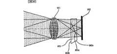
図30は、輝度ムラが生じる様子を示した光学機器の模式図である。同図において、901は結像光学系、902は写真フィルムやCCDセンサーなどであって、可視光に対してのみ感度を有する受光素子、903はビームスプリッターである。受光素子902で撮像された画像は、フィルムカメラであれば現像されて写真原版となり、デジタルカラーカメラであれば電子ビューファインダー(EVF)に表示されたり、メモリに記録されたり、あるいはプリンターに出力されたりする。 FIG. 30 is a schematic diagram of an optical apparatus illustrating a state in which luminance unevenness occurs. In the figure,
ビームスプリッター903の光分割機能面903aには誘電体多層膜が形成され、結像光学系901にて射出された物体光の可視光成分のうち、50%が反射され、残りの50%を透過する。光分割機能面903aで反射された光は、ビームスプリッター903の面903bで全反射し、面903cを通ってビームスプリッター903の外部に射出される。 A dielectric multilayer film is formed on the light splitting function surface 903a of the
この光学機器が、例えば赤外線カメラの場合には、受光素子902は赤外線に対してのみ感度を有し、ビームスプリッター903の光分割機能面903aでは赤外線を分割する様に構成する。 When this optical device is, for example, an infrared camera, the light receiving element 902 has sensitivity only to infrared rays, and the light splitting functional surface 903a of the
図30において、光分割機能面903aを通過した可視光は前述のように1/2に減衰しているので、仮に、撮像の対象物が均一輝度面であったとすると、受光素子によって撮像された画像は、図31に示す如く、中央の暗い領域911を挟んで上下に明るい領域912と913が形成された画像910のようになってしまう。こういった現象は、特に青空や建物の白壁などを撮影した場合に均一輝度であるはずの部分に不自然な輝度差が目立ち、たいへん品位を損なった画像となって好ましくない。 In FIG. 30, since the visible light that has passed through the light splitting function surface 903a is attenuated to ½ as described above, if the object to be imaged is a uniform luminance surface, the image is picked up by the light receiving element. As shown in FIG. 31, the image looks like an
一方、特許文献2では、ビームスプリッターで大部分の光を直進させることによって撮像した画像に輝度ムラが生じないようにしている。すなわち、直進した大部分の光を撮像に供し、残りの光で焦点検出を行う構成になっている。このようにすると、画像の輝度ムラはある程度解消できるものの焦点検出のための光量が十分ではなくなり、低輝度の物体に対する焦点調節精度が不足する。 On the other hand, in
本発明は、機器を大型化することなく、ビームスプリッターを透過した光に基づく高品位の画像を得ることのできる光学機器およびビームスプリッターを提供することを目的の1つとしている。 An object of the present invention is to provide an optical device and a beam splitter that can obtain a high-quality image based on light transmitted through the beam splitter without increasing the size of the device.
1つの側面としての本発明の光学機器は、所定波長域の光に対して感度を有する受光素子と、入射光軸に対して傾斜角度を持ち、前記所定波長域の入射光のうち一部の光束を反射し他の光束を前記受光素子へ透過する第1の面、および、前記入射光軸に対して直交するように前記第1の面に接して形成され、前記第1の面への入射光以外の前記所定波長域の入射光を前記受光素子へ透過する第2の面を有したビームスプリッターとを有する。そして、前記所定波長域に対する前記第2の面の透過率を、実質的に均一な輝度分布を有する物体からの前記所定波長域の光が前記第1および第2の面に入射した場合の前記受光素子上での光量分布が実質的に均一な分布となるように設定したことを特徴とする。 An optical apparatus according to the present invention as one aspect includes a light receiving element having sensitivity to light in a predetermined wavelength range, an inclination angle with respect to an incident optical axis, and a part of incident light in the predetermined wavelength range. A first surface that reflects a light beam and transmits another light beam to the light-receiving element; and is formed in contact with the first surface so as to be orthogonal to the incident optical axis; A beam splitter having a second surface that transmits incident light in the predetermined wavelength region other than incident light to the light receiving element. Then, the transmittance of the second surface with respect to the predetermined wavelength region is determined based on the case where light in the predetermined wavelength region from an object having a substantially uniform luminance distribution is incident on the first and second surfaces. It is characterized in that the light amount distribution on the light receiving element is set to be a substantially uniform distribution.
また、他の側面としての本発明の光学機器は、所定波長域の光に対して感度を有する受光素子と、入射光軸に対して傾斜角度を持ち、前記所定波長域の入射光のうち一部の光束を反射し他の光束を前記受光素子へ透過する第1の面、および、前記入射光軸に対して直交するように前記第1の面に接して形成され、前記第1の面への入射光以外の前記所定波長域の入射光を前記受光素子へ透過する第2の面を有したビームスプリッターとを有する。さらに、実質的に均一な輝度分布を有する物体からの光が前記第1および第2の面に入射した場合の前記受光素子からの出力に対するゲインを調節して、該調節後の出力分布を実質的に均一な分布とするゲイン補正部を有することを特徴とする。 An optical device according to another aspect of the present invention includes a light receiving element having sensitivity to light in a predetermined wavelength region, an inclination angle with respect to an incident optical axis, and one of the incident light in the predetermined wavelength region. A first surface that reflects a light beam of a portion and transmits another light beam to the light receiving element, and is formed in contact with the first surface so as to be orthogonal to the incident optical axis, and the first surface And a beam splitter having a second surface that transmits incident light in the predetermined wavelength region other than incident light to the light receiving element. Further, by adjusting the gain for the output from the light receiving element when light from an object having a substantially uniform luminance distribution is incident on the first and second surfaces, the output distribution after the adjustment is substantially And a gain correction unit having a uniform distribution.
また、他の側面としての本発明の光学機器は、所定波長域の光に対して感度を有する受光素子と、前記所定波長域の入射光のうち一部の光束を反射し他の光束を前記受光素子へ透過する光分離面を含む第1の領域、および、前記第1の領域への入射光以外の前記所定波長域の入射光を前記受光素子へ透過する第2の領域を有するビームスプリッターとを有する。そして、前記所定波長域に対する前記第2の領域の透過率を、前記所定波長域に対する前記第1の領域の透過率と実質的に同一としたことを特徴とする。 An optical device according to another aspect of the present invention includes a light receiving element having sensitivity to light in a predetermined wavelength range, and reflects a part of light flux of incident light in the predetermined wavelength range, A beam splitter having a first region including a light separation surface that transmits to the light receiving element, and a second region that transmits incident light in the predetermined wavelength region other than the incident light to the first region to the light receiving element. And have. The transmittance of the second region with respect to the predetermined wavelength region is substantially the same as the transmittance of the first region with respect to the predetermined wavelength region.
また、他の側面としての本発明のビームスプリッターは、所定波長域の入射光のうち一部の光束を反射し他の光束を透過する光分離面を含む第1の領域と、前記第1の領域への入射光以外の前記所定波長域の入射光を前記受光素子へ透過する第2の領域とを有する。そして、前記所定波長域に対する前記第2の領域の透過率を、前記所定波長域に対する前記第1の領域の透過率と実質的に同一としたことを特徴とする。 The beam splitter according to another aspect of the present invention includes a first region including a light separation surface that reflects a part of a light beam and transmits another light beam in incident light in a predetermined wavelength range, and the first region. A second region that transmits incident light in the predetermined wavelength region other than incident light to the region to the light receiving element. The transmittance of the second region with respect to the predetermined wavelength region is substantially the same as the transmittance of the first region with respect to the predetermined wavelength region.
さらに、他の側面としての本発明の光学機器は、所定波長域の光に対して感度を有する受光素子と、前記所定波長域の入射光のうち一部の光束を反射し他の光束を前記受光素子へ透過する光分離面を含む第1の領域、および、前記第1の領域への入射光以外の前記所定波長域の入射光を前記受光素子へ透過する第2の領域を有するビームスプリッターとを有する。さらに、実質的に均一な輝度分布を有する物体からの前記所定波長域の光が前記第1および第2の領域に入射した場合に前記受光素子を用いて得られる画像の輝度分布を実質的に均一な分布とするための画像処理を行う処理部を有することを特徴とする。 Furthermore, an optical device according to another aspect of the present invention includes a light receiving element having sensitivity to light in a predetermined wavelength range, and reflects a part of light flux of incident light in the predetermined wavelength range, A beam splitter having a first region including a light separation surface that transmits to the light receiving element, and a second region that transmits incident light in the predetermined wavelength region other than the incident light to the first region to the light receiving element. And have. Further, the luminance distribution of an image obtained by using the light receiving element when light in the predetermined wavelength range from an object having a substantially uniform luminance distribution is incident on the first and second regions is substantially reduced. It has a processing part which performs image processing for making it into uniform distribution.
本発明のさらなる目的又は特徴は、以下の図面を参照して説明される好ましい実施例により明らかにされるであろう。 Further objects or features of the present invention will become apparent from the preferred embodiments described with reference to the following drawings.
本発明によれば、機器又はビームスプリッターを大型化することなく、ビームスプリッターを透過した光を受けた受光素子の出力に基づいて高品位の画像を得ることができる。 According to the present invention, it is possible to obtain a high-quality image based on the output of the light receiving element that has received the light transmitted through the beam splitter without increasing the size of the device or the beam splitter.
[図1]本発明の実施例1に係るデジタルカラーカメラを示す断面図である。
[図2]図1のデジタルカラーカメラの電気的構成を示すブロック図である。
[図3]図1のデジタルカラーカメラのレンズ鏡筒部分を示す断面図である。
[図4]図1のデジタルカラーカメラに具備されるビームスプリッターの断面図であ る。
[図5]図1のデジタルカラーカメラに具備されるビームスプリッターの斜視図であ る。
[図6]図1のデジタルカラーカメラに具備されるビームスプリッターの分解斜視図である。
[図7]図1のデジタルカラーカメラに具備される光分割機能面103aの光学特性 を示す図である。
[図8]図1のデジタルカラーカメラに具備されるNDフィルターの光学特性の例を 示す図である。
[図9]図1のデジタルカラーカメラに具備される焦点検出用センサー112による 焦点検出視野を示す図である。
[図10]図1のデジタルカラーカメラに具備される焦点検出用センサーの平面図である。
[図11]図1のデジタルカラーカメラに具備される受光センサー108の画素部の 断面図である。
[図12]図1のデジタルカラーカメラに具備される受光センサー108の1画素の 光電変換部及び1画素の平面図である。
[図13]図12に示した画素を連結して焦点検出に使用するための画素列とした状態を表す平面図である。
[図14]図12に示した画素を連結して焦点検出に使用するための画素列とした状態を表す斜視図である。
[図15]図1のデジタルカラーカメラに具備される第1配線層154の開口154A、154Bを示す平面図である。
[図16]図10に示した焦点検出視野112−1の部分断面図である。
[図17]図10に示した焦点検出視野112−1の部分断面図である。
[図18]図1のデジタルカラーカメラに具備されるAF制御部40に入力された焦 点検出用センサーの出力信号波形を示す図である。
[図19]図1のデジタルカラーカメラに具備されるAF制御部40に入力された焦 点検出用センサーの出力信号波形を示す図である。
[図20]図1のデジタルカラーカメラに具備される結像光学系102の射出瞳上で の焦点検出光束の通過領域を説明するための図である。
[図21]図1のデジタルカラーカメラに係わる撮影光束の説明図である。
[図22]図1のデジタルカラーカメラに係わる焦点検出光束を描いたビームスプリッター部の断面図である。
[図23]図1のデジタルカラーカメラに係わる画像上の輝度ムラの発生度合いを示す図である。
[図24]図1のデジタルカラーカメラに係わる画像上の輝度ムラの発生度合いを示す図である。
[図25]図1のデジタルカラーカメラに係わるビームスプリッター103と光学ローパスフィルター113が入れ代わった状態を示す図である。
[図26]本発明の実施例2に係わるデジタルカラーカメラの画像処理回路131に おける信号処理を表すフローチャートである。
[図27]本発明の実施例2に係わるデジタルカラーカメラの画面上の位置とゲインとの関係を表す図である。
[図28]本発明の実施例2に係わるデジタルカラーカメラのゲイン適用後の信号のレベルを示す図である。
[図29]従来のデジタルカラーカメラの画像上の輝度ムラの発生度合いを示す図である。
[図30]従来のデジタルカラーカメラの輝度ムラが生じる様子を示した光学機器の模式図である。
[図31]従来のデジタルカラーカメラの画像上の輝度ムラの発生度合いを示す図である。FIG. 1 is a cross-sectional view showing a digital color camera according to
FIG. 2 is a block diagram showing an electrical configuration of the digital color camera of FIG.
3 is a cross-sectional view showing a lens barrel portion of the digital color camera of FIG.
4 is a sectional view of a beam splitter provided in the digital color camera of FIG.
FIG. 5 is a perspective view of a beam splitter provided in the digital color camera of FIG.
6 is an exploded perspective view of a beam splitter provided in the digital color camera of FIG.
FIG. 7 is a diagram showing optical characteristics of a light dividing
FIG. 8 is a diagram showing an example of optical characteristics of an ND filter provided in the digital color camera of FIG.
9 is a view showing a focus detection field of view by the
10 is a plan view of a focus detection sensor provided in the digital color camera of FIG.
11 is a cross-sectional view of a pixel portion of a
FIG. 12 is a plan view of a one-pixel photoelectric conversion unit and one pixel of the
FIG. 13 is a plan view showing a state in which the pixels shown in FIG. 12 are connected to form a pixel row for use in focus detection.
FIG. 14 is a perspective view showing a state in which the pixels shown in FIG. 12 are connected to form a pixel row for use in focus detection.
15 is a plan
FIG. 16 is a partial cross-sectional view of focus detection visual field 112-1 shown in FIG.
FIG. 17 is a partial cross-sectional view of focus detection visual field 112-1 shown in FIG.
[FIG. 18] A diagram showing an output signal waveform of a focus detection sensor input to an
FIG. 19 is a diagram showing an output signal waveform of a focus detection sensor input to an
20 is a diagram for explaining a passing region of a focus detection light beam on an exit pupil of an imaging
FIG. 21 is an explanatory diagram of photographing light flux related to the digital color camera of FIG.
FIG. 22 is a cross-sectional view of a beam splitter section depicting a focus detection light beam related to the digital color camera of FIG.
FIG. 23 is a diagram showing a degree of occurrence of luminance unevenness on an image related to the digital color camera of FIG.
FIG. 24 is a diagram showing a degree of occurrence of luminance unevenness on an image related to the digital color camera of FIG.
FIG. 25 is a diagram showing a state in which the
FIG. 26 is a flowchart showing signal processing in the
FIG. 27 is a diagram illustrating a relationship between a position on a screen and a gain of a digital color camera according to
FIG. 28 is a diagram showing signal levels after gain application in a digital color camera according to
FIG. 29 is a diagram showing a degree of occurrence of luminance unevenness on an image of a conventional digital color camera.
FIG. 30 is a schematic diagram of an optical apparatus showing how luminance unevenness occurs in a conventional digital color camera.
FIG. 31 is a diagram showing a degree of occurrence of luminance unevenness on an image of a conventional digital color camera.
以下、本発明の好ましい実施例について図面を参照しながら説明する。 Hereinafter, preferred embodiments of the present invention will be described with reference to the drawings.
図1から図25には、本発明の実施例1に係るデジタルカラーカメラ(光学機器)に関する図である。 1 to 25 are diagrams relating to a digital color camera (optical apparatus) according to
まず、図1はデジタルカラーカメラの断面図であって、焦点調節を行ってEVF(Electric View Finder)用画像を取り込む状態を示している。図1において、101はデジタルカラーカメラ本体、102は物体像を形成するための結像光学系、104は結像光学系101の光軸、105は結像光学系102を収納するレンズ鏡筒である。結像光学系102は不図示のエネルギー源と不図示の駆動機構により結像位置を光軸104の方向に調節可能である。フォーカシングレンズを柔軟性のある透明弾性部材や液体レンズで構成し、界面形状を変化させて屈折力を変えることで、物体にピントを合わせることもできる。結像光学系102は単焦点レンズ、ズームレンズ、あるいはシフトレンズ等であっても良い。また、種々の特性(Fナンバーや焦点距離など)をもった結像光学系に交換可能であっても良い。 First, FIG. 1 is a cross-sectional view of a digital color camera, and shows a state where an image for EVF (Electric View Finder) is captured by performing focus adjustment. In FIG. 1, 101 is a digital color camera body, 102 is an imaging optical system for forming an object image, 104 is an optical axis of the imaging
結像光学系102を構成するレンズの材質としてアクリル樹脂に大きさが5nmから30nm程度の酸化ニオブ粒子を均一に分散させたコンポジット材を使用すると、屈折率が1.8程度と高屈折率でありながらガラスよりも衝撃に強く、しかも、射出成形で安価に製造可能である。 When a composite material in which niobium oxide particles having a size of about 5 nm to 30 nm are uniformly dispersed in an acrylic resin is used as the material of the lens constituting the imaging
103はビームスプリッター、111はシャッターレリーズボタン、107はディスプレイ装置、108は画像データを格納するメモリーカード、109は光学ファインダーの接眼レンズ、110はプリンター等とのデータ通信を行う無線通信装置、106は2次元型CMOS受光センサー、112は焦点検出用センサー、113は光学ローパスフィルターである。 103 is a beam splitter, 111 is a shutter release button, 107 is a display device, 108 is a memory card for storing image data, 109 is an eyepiece of an optical viewfinder, 110 is a wireless communication device for data communication with a printer, 106 A two-dimensional CMOS light receiving sensor, 112 is a focus detection sensor, and 113 is an optical low-pass filter.
ビームスプリッター103と光学ローパスフィルター113は、不図示の駆動機構によって、高精細画像の撮像時には図25に示す如くビームスプリッター103のあった位置に、該ビームスプリッター103と置き換わるように光学ローパスフィルター113が挿入される。つまり、EVF用画像の取り込み時にはビームスプリッター103を透過した光束が、高精細画像の撮像時には光学ローパスフィルター113を透過した光束が、それぞれCMOS受光センサー106上に投影されるようになっている。 The
ディスプレイ装置107はカメラの背面に取り付けられており、CMOS受光センサー106で捉えられた物体像がディスプレイ装置107上に表示される。使用者はEVFとして直接これを観察することができる。ディスプレイ装置107は有機EL空間変調素子や液晶空間変調素子、微粒子の電気泳動を利用した空間変調素子などで構成すると消費電力が小さくかつ薄型で都合が良い。 The
CMOS受光センサー106は、増幅型固体撮像素子の1つであるCMOSプロセスコンパチブルのセンサー(以下、CMOSセンサーと略す)である。CMOSセンサーの利点の1つに、エリアセンサ部のMOSトランジスタと撮像素子駆動回路、AD変換回路、画像処理回路といった周辺回路を同一工程で形成できるため、マスク枚数、プロセス工程がCCDと比較して大幅に削減できるということが挙げられる。また、任意の画素へのランダムアクセスが可能という特長も有し、画素を間引いた読み出しを行うと高い表示レートで画像のリアルタイム表示が行える。 The CMOS
CMOS受光センサー106は、この特長を利用し、間引き読み出しによるEVF用画像出力動作と全ての画素を読み出す高精彩画像出力動作を行う。 Using this feature, the CMOS
図2はデジタルカラーカメラの電気的構成を示すブロック図である。まず、物体像の撮像、記録に関する部分から説明する。カメラは、撮像系、画像処理系、記録再生系、制御系を有する。撮像系は、結像光学系102、CMOS受光センサー106を含み、画像処理系は、A/D変換器130、RGB画像処理回路131およびYC処理回路132を含む。また、記録再生系は、記録処理回路133および再生処理回路134を含み、制御系は、カメラシステム制御回路135、操作検出回路136およびCMOS受光センサー駆動回路137を含む。138は外部のコンピュータ等に接続して、データの送受信をするための規格化された接続端子である。これらの電気回路は不図示の小型燃料電池によって駆動される。 FIG. 2 is a block diagram showing an electrical configuration of the digital color camera. First, an explanation will be given from the part related to the imaging and recording of object images. The camera has an imaging system, an image processing system, a recording / reproducing system, and a control system. The imaging system includes an imaging
撮像系は、物体からの光を結像光学系102を介してCMOS受光センサー106の撮像面に結像する光学処理系であり、結像光学系102の不図示の絞りとメカニカルシャッターを調節し、適切な光量の物体光をCMOS受光センサー106に露光する。CMOS受光センサー106は、正方画素が長辺方向に3700個、短辺方向に2800個並べられ、合計約1000万個の画素数を有する受光素子が適用され、各画素にR(赤色)G(緑色)B(青色)のカラーフィルターを交互に配して4画素が一組となる所謂ベイヤー配列を形成している。 The imaging system is an optical processing system that forms an image of light from an object on the imaging surface of the CMOS
ベイヤー配列では、観察者が画像を見たときに強く感じやすいGの画素をRやBの画素よりも多く配置する事で、総合的な画像性能を上げている。一般に、この方式の撮像素子を用いる画像処理では、輝度信号の多くの部分をGから生成し、色信号はR,G,Bから生成する。 In the Bayer array, the overall image performance is improved by arranging more G pixels that are easily felt when an observer looks at the image than R and B pixels. In general, in image processing using this type of image sensor, a large portion of a luminance signal is generated from G, and a color signal is generated from R, G, and B.
CMOS受光センサー106から読み出された画像信号は、A/D変換器130を介して画像処理系に供給される。A/D変換器130は、露光した各画素の信号の振幅に応じた、たとえば12ビットのデジタル信号に変換して出力する信号変換回路であり、これ以降の画像信号処理はデジタル処理にて実行される。 The image signal read from the CMOS
画像処理系は、R,G,Bのデジタル信号から所望の形式の画像信号を得る信号処理回路であり、R,G,Bの色信号を輝度信号Yおよび色差信号(R−Y),(B−Y)にて表わされるYC信号などに変換する。 The image processing system is a signal processing circuit that obtains an image signal of a desired format from R, G, and B digital signals. The R, G, and B color signals are converted into a luminance signal Y and a color difference signal (R−Y), ( B-Y) and the like are converted into a YC signal.
RGB画像処理回路131は、A/D変換器130を介してCMOS受光センサー106から受けた3700×2800画素の画像信号を処理する信号処理回路であり、ホワイトバランス回路、ガンマ補正回路、補間演算による高解像度化を行う補間演算回路を有する。 The RGB
YC処理回路132は、輝度信号Yおよび色差信号R−Y,B−Yを生成する信号処理回路である。高域輝度信号YHを生成する高域輝度信号発生回路、低域輝度信号YLを生成する低域輝度信号発生回路、および、色差信号R−Y,B−Yを生成する色差信号発生回路で構成されている。輝度信号Yは高域輝度信号YHと低域輝度信号YLを合成することによって形成される。 The
記録再生系は、メモリへの画像信号の出力と、ディスプレイ装置107への画像信号の出力とを行う処理系であり、記録処理回路133はメモリへの画像信号の書き込み処理および読み出し処理を行い、再生処理回路134はメモリから読み出した画像信号を再生して、ディスプレイ装置107に出力する。 The recording / reproducing system is a processing system that outputs the image signal to the memory and the image signal to the
また、記録処理回路133は、静止画像および動画像を表わすYC信号を所定の圧縮形式にて圧縮し、また、圧縮データを読み出した際に伸張する圧縮伸張回路を内部に有する。圧縮伸張回路は、信号処理のためのフレームメモリなどを含み、このフレームメモリに画像処理系からのYC信号を1画像毎に蓄積して、それぞれ複数のブロック毎に読み出して圧縮符号化する。圧縮符号化は、たとえば、ブロック毎の画像信号を2次元直交変換、正規化およびハフマン符号化することにより行われる。 The
再生処理回路134は、輝度信号Yおよび色差信号R−Y,B−Yをマトリックス変換して、例えばRGB信号に変換する回路である。再生処理回路134によって変換された信号はディスプレイ装置107に出力され、可視画像が表示再生される。再生処理回路134とディスプレイ装置107の間、あるいはプリンターとの間はBluetoothなどの無線通信手段を介して接続されてもよく、このように構成すれば、このデジタルカラーカメラで撮像する画像を離れたところからモニターしたり、撮影した画像をパーソナルコンピューターを介さずに印刷したりすることができる。 The
制御系は、シャッターレリーズボタン111等の操作を検出する操作検出回路136と、その検出信号に応動して各部を制御し、撮像の際のタイミング信号などを生成して出力するカメラシステム制御回路135と、このカメラシステム制御回路135の制御の下にCMOS受光センサー106を駆動する駆動信号を生成するCMOS受光センサー駆動回路137と、光学ファインダー内の情報表示装置やカメラの外面にある情報表示装置を制御する情報表示回路142を含む。 The control system includes an
制御系は、外部操作に応動して撮像系、画像処理系、記録再生系をそれぞれ制御し、例えば、シャッターレリーズボタン111の押下を検出して、CMOS受光センサー106の駆動、RGB画像処理回路131の動作、記録処理回路133の圧縮処理などを制御し、さらに情報表示回路142によって光学ファインダー等に情報表示を行う情報表示装置の各セグメントの状態を制御する。 The control system controls the imaging system, the image processing system, and the recording / reproducing system in response to external operations, for example, detects the depression of the shutter release button 111, drives the CMOS
カメラシステム制御回路135にはさらにAF制御回路140とレンズシステム制御回路141が接続されている。これらはカメラシステム制御回路135を中心にして各々の処理に必要とするデータを相互に通信している。 An AF control circuit 140 and a lens system control circuit 141 are further connected to the camera
AF制御回路140は、撮影画面上の所定位置に対応して設定された焦点検出用センサー112の焦点検出視野の信号出力を得て焦点検出信号を生成し、結像光学系102の結像状態を検出する。デフォーカスが検出されると、これを結像光学系102の一部の要素であるフォーカシングレンズの駆動量に変換し、カメラシステム制御回路135を中継してレンズシステム制御回路141に送信する。また、移動する物体に対しては、シャッターレリーズボタン111が押下されてから実際の撮像制御が開始されるまでのタイムラグを勘案し、適切なレンズ位置を予測してフォーカシングレンズ駆動量を指示する。物体の輝度が低く、十分な焦点検出精度が得られないと判定されるときには、不図示の閃光発光装置、あるいは不図示の白色LEDや蛍光管によって物体を照明し、不足していた輝度を補う。 The AF control circuit 140 obtains a signal output of the focus detection field of the
レンズシステム制御回路141は、フォーカシングレンズの駆動量を受信すると、不図示の駆動機構によって結像光学系102内のフォーカシングレンズを光軸方向に移動させて、物体にピントを合わせる。 When receiving the driving amount of the focusing lens, the lens system control circuit 141 moves the focusing lens in the imaging
一連のピント調節動作の結果、AF制御回路140によって、物体にピントが合ったことが検出されると、この情報はカメラシステム制御回路135に伝えられる。このとき、シャッターレリーズボタン111が2段目まで押下されれば、不図示の機構によってビームスプリッター103と光学ローパスフィルター113が入れ代わり、高精細画像が光学ローパスフィルター113を透過した光束で形成されて、前述のごとく撮像系、画像処理系、記録再生系による撮像制御が成される。この際、結像光学系102のピント変動が生じないように、ビームスプリッター103があった位置に光学ローパスフィルター113が挿入されるので、ピントの補正をする必要は無い。したがって、高速な焦点検出動作を損ねることなく短いレリーズタイムラグを実現できる。 As a result of a series of focus adjustment operations, when the AF control circuit 140 detects that the object is in focus, this information is transmitted to the camera
図3はデジタルカラーカメラ101のレンズ鏡筒105部分の断面図、図4はビームスプリッター103の断面図、図5はビームスプリッター103の斜視図、図6はビームスプリッター103の分解斜視図である。これらの図を用いてビームスプリッター103とその周辺部分について詳述する。 3 is a sectional view of the
ビームスプリッター103は結像光学系102を構成するレンズ102aと102bの間に位置する。レンズ102aはフォーカシングレンズであって、光軸104方向に移動することで、ピント調節を行う。 The
CMOS受光センサー106はレンズ102bに対して位置決めされ、CMOS受光センサー106のカバーガラス106aが封止部材115を介して固定されている。こういった構成を採ることで、CMOS受光センサー106のカバーガラス106aに塵が付着する可能性はなく、塵の付着する可能性があるとすれば、レンズ102bの入射面となる。CMOS受光センサー106の受光面から塵の位置までは十分長いので、レンズ102bの入射面に付着した塵が画面に写り込むことはほとんどない。 The CMOS
また、可視波長域においてビームスプリッター103の光学長は光学ローパスフィルター113の光学長に一致させてあり、図3に示したビームスプリッター103が退避して、その位置に光学ローパスフィルター113が挿入された時にも、結像光学系102のCMOS受光センサー106上への結像状態は変化しない。 In the visible wavelength range, the optical length of the
概略の撮像シーケンスは次の通りである。シャッターレリーズボタン111の第1段階押下を検出したら、CMOS受光センサー106を駆動してビームスプリッター103を透過した光束によって物体像を繰り返し撮像し、ディスプレイ装置107に物体像のリアルタイム表示を行い、EVFとして動作させる(図1の状態)。ビームスプリッター103で分割した可視波長域の光束によって、焦点検出を行う。所定量以上のデフォーカスが検出されたら、フォーカシングのレンズ102aの駆動量を算出し、その量だけレンズ102aを動かして焦点調節を行う。デフォーカス量が所定の範囲内にあることを確認したら、音や光による合焦表示を出す。シャッターレリーズボタン111の第2段階押下を検出したら、不図示の機構によりビームスプリッター103を結像光学系102の光路から退避させ、代わりに光学ローパスフィルター113を挿入する(図25の状態)。CMOS受光センサー106を駆動して高精細モードでの撮像を行う。その後、光学ローパスフィルター113を結像光学系102の光路から退避させて、ビームスプリッター103を元の位置に戻す(図1の状態)。撮像された物体像に関する画像データをメモリに書き込む。 A schematic imaging sequence is as follows. When the first release of the shutter release button 111 is detected, the CMOS
さて次に、図3〜図6を用いて光分割機能について詳述する。ビームスプリッター103は2つのプリズム103−1と103−2を光分割機能面103aで貼り合せたものである。ビームスプリッター103の光入射面は、プリズム103−1の面103−1bとプリズム103−2の面103−2bで構成され、直進光の射出面はプリズム103−1の面103−1dとプリズム103−2の面103−2dで構成されている。プリズム103−1の面103−1bとプリズム103−2の面103−2bの段差や、プリズム103−1の面103−1dとプリズム103−2の面103−2dの段差はない。また、プリズム103−1の面103−1bと面103−1d、および、プリズム103−2の面103−2bと面103−2dは平行である。したがって、ビームスプリッター103は直進する光に対し平行平板として機能する。 Next, the light splitting function will be described in detail with reference to FIGS. The
プリズム103−1の面103−1bと光分割機能面103a(103−1a)、および、プリズム103−2の面103−2dと光分割機能面103a(103−2a)とは異なる傾斜角度を有し、プリズム103−1の面103−1bと光分割機能面103a、および、プリズム103−2の面103−2dと光分割機能面103aはそれぞれ鈍角をなして接する。 The surface 103-1b and the light splitting
ビームスプリッター103の光分割機能面103aは、所望の光学特性を得るためにプリズム103−2の面103−2a上に誘電体多層膜を形成し、インデックスマッチング(屈折率整合)をとった光学用接着剤を用いてプリズム103−1と貼り合せることによって形成する。光分割機能面103aの光学特性は図7に示す通りであって、波長400nmから1000nmまでの分光透過率特性は500nm付近に極小値を持つ谷型、一方、分光反射率特性は500nm付近に極大値を持つ山型である。すなわち、所定波長域の入射光のうちの一部を反射し他の一部を透過する。誘電体多層膜の特徴として、吸収をほとんど無視できる程に小さく出来るので、光分割機能面103aにおいて入射光はCMOS受光センサーか焦点検出用センサーかの何れかの方向に分かれることになる。 The light
ここで、450nmから650nmまでの可視域についてみると分光透過率特性はおよそ45%となっている。カラーカメラではCMOS受光センサー106の感度域を視感度域に合致させるので、CMOS受光センサー106の感度波長域では分光透過率特性がフラットであると言える。 Here, in the visible region from 450 nm to 650 nm, the spectral transmittance characteristic is about 45%. In the color camera, the sensitivity range of the CMOS
プリズム103−1の面103−1bとプリズム103−2の面103−2bによる光入射面からビームスプリッター103の内部に入射した光束のうち、光分割機能面103aで反射した光束は、プリズム103−2の面103−2bで全反射して、面103−2cから射出する。面103−2cに対向する位置には、焦点検出に使用する光束を集める働きをするコンデンサーレンズ114が配置され、コンデンサーレンズ114を透過した光が焦点検出用センサー112に入射し、これによって焦点検出機能が動作する。 Of the light beams incident on the inside of the
このように、特許文献1に記載された技術との対比において、ビームスプリッター103で分割された光束の分光特性(分光反射率特性)を直進光の分光特性(分光透過率特性)と実質的に同一としてあり、この光束によって焦点検出機能を動作させる。ここでの分光反射率特性はおよそ55%であるので、十分な光量により高精度な焦点検出が可能である。 Thus, in contrast with the technique described in
なお、焦点検出用センサー112の分光感度を厳密にCMOS受光センサー106に合わせるために、コンデンサーレンズ114に赤外線カット機能を付加しておくとさらに良い。 In order to precisely match the spectral sensitivity of the
プリズム103−1の面103−1bとプリズム103−2の面103−2bには、ND(Neutral Density)フィルターが形成されている。NDフィルターは一種の光吸収膜で、クロメルなどの蒸着膜が用いられ、非常に広い波長域に対してフラットな透過特性を得ることが出来る。クロメルはニッケル(Ni)を主成分とした合金で、Cr:7.0〜10.5%、Mn:1.5%以下、Si:1.0以下、といった組成比を有する。 An ND (Neutral Density) filter is formed on the surface 103-1b of the prism 103-1 and the surface 103-2b of the prism 103-2. The ND filter is a kind of light absorption film, and a vapor deposition film such as chromel is used, and a flat transmission characteristic can be obtained over a very wide wavelength range. Chromel is an alloy containing nickel (Ni) as a main component and has a composition ratio of Cr: 7.0 to 10.5%, Mn: 1.5% or less, Si: 1.0 or less.
図8はクロメルの蒸着膜を用いたNDフィルターの光学特性の例である。450nmから650nmまでの可視域についてみると分光透過率はおよそ45%で一定であり、吸収が多いのでこの間の分光反射率はおよそ15%となる。 FIG. 8 is an example of optical characteristics of an ND filter using a chromel deposited film. In the visible region from 450 nm to 650 nm, the spectral transmittance is constant at about 45%, and since there is much absorption, the spectral reflectance during this period is about 15%.
次に、焦点検出用センサー112について説明する。図9は焦点検出用センサー112による焦点検出視野を示す図である。図9において、120は撮像範囲を観察範囲としたファインダー視野、121−1から121−9は焦点検出視野である。焦点検出視野は撮像範囲の中央付近に設定すると使い勝手が良いカメラとなる。縦方向の画素列によって構成された焦点検出視野は、縦方向の輝度分布に対して感度があるので、例えば、横線に対する焦点検出が可能であり、他方、横方向の画素列によって構成された焦点検出視野は、横方向の輝度分布に対して感度があるので、例えば、縦線に対する焦点検出が可能である。 Next, the
実際の焦点検出用センサー112は、図10のように構成される。図10は焦点検出用センサー112の平面図であって、112−1から112−9は焦点検出視野121−1から121−9を構成する画素列である。 The actual
では、焦点検出用センサー112の構造について説明する。図11はセンサー112の画素部の断面図、図12(a)はセンサー112の1画素の光電変換部を表す平面図、図12(b)はセンサー112の1画素のマイクロレンズを表わす平面図である。光は図11においては上方から焦点検出用センサー112に入射し、図12(a),(b)においては紙面手前方向から焦点検出用センサー112に入射する。焦点検出用センサー112はオンチップ型マイクロレンズを有するCMOS型のセンサーで、このマイクロレンズの働きで焦点検出光束のFナンバーを規定できる。 Now, the structure of the
図11において、151はシリコン基板、152Aと152Bは埋め込みフォトダイオードの光電変換部、154はアルミニウムあるいは銅による遮光性を有する第1配線層、155はアルミニウムあるいは銅を用いた第2配線層、156はシリコン酸化膜、疎水性多孔質シリカ、シリコン酸化窒化膜、あるいはシリコン窒化膜などによる層間絶縁膜とパッシベーション膜、158はマイクロレンズ、157は第2配線層155からマイクロレンズ158までの距離を高精度に設定するための平坦化層である。第1配線層154と第2配線層155は離散的に設けられた開口を備えた金属膜であって、開口以外は可視光を通さない。第1配線層154と第2配線層155は焦点検出用センサー112を動作させる電気的な機能と受光光束の角度特性を制御する光学的な機能を併せ持っている。平坦化層157は熱硬化型の樹脂や紫外線硬化型の樹脂をスピンコートした後にキュアするとか、樹脂フィルムを接着するといった手法で形成する。 In FIG. 11, 151 is a silicon substrate, 152A and 152B are photoelectric conversion portions of embedded photodiodes, 154 is a first wiring layer having light shielding properties by aluminum or copper, 155 is a second wiring layer using aluminum or copper, 156 Is an interlayer insulating film and passivation film made of silicon oxide film, hydrophobic porous silica, silicon oxynitride film, or silicon nitride film, 158 is a microlens, 157 is a high distance from the
光電変換部152A,152Bは、図12(a)に示すように、ジグザグ形をしており、端部にはそれぞれ回路部159A,159Bが接続されている。回路部159A,159B内には転送スイッチとして働く転送用MOSトランジスタ、リセット電位を供給するリセット用MOSトランジスタ、ソースフォロワアンプMOSトランジスタ、選択的にソースフォロワアンプMOSトランジスタから信号を出力させるための選択用MOSトランジスタ等を有する。光電変換部152の上には、図12(b)に示すように、1画素につき5個のマイクロレンズ158がやはリジグザグ形に連なって設けられている。 As shown in FIG. 12A, the
ここで、マイクロレンズ158は、樹脂、SiO2,TiO2,Si3N4などで形成され、単に集光のためではなく結像のために使用するので回転対称型の球面レンズ、あるいは回転対称型の非球面レンズである。対称軸160を持つ形状であるために平面的に見ると円形であるが、一画素に複数のマイクロレンズを設けたことによって、画素ピッチを小さくしながらも1画素の受光面積を大きくすることが出来ている。したがって、低輝度の物体に対しても十分な受光センサー出力が得られる。また、例えば半円筒形など回転対称軸を持たない形状はレンズとしての結像作用が無いので、この焦点検出用センサー112には適当でない。なお、マイクロレンズ158には、光の表面反射を抑制するために、マイクロレンズの表面に低屈折率の薄膜や可視光の波長以下の微細構造(所謂Sub−Wavelength Structure)を形成しても良い。Here, the
コンデンサーレンズ114より射出された光束は焦点検出用センサー112のマイクロレンズ158に先ず入射し、次に第2配線層155に設けられた開口155aと第1配線層154に設けられた開口154Aを通り抜けた成分が光電変換部152Aに入射し、第2配線層155に設けられた開口155aと第1配線層154に設けられた開口154Bを通り抜けた成分が光電変換部152Bに入射して、それぞれ電気信号に変換される。開口を形成するための遮光層と第1配線層および第2配線層を兼用したので、開口のための遮光層を特別に設ける必要が無く受光センサーの構成を簡略化することが出来ている。 The light beam emitted from the
図13と図14は、図12に示した画素を連結して焦点検出に使用するための画素列とした状態を表す平面図と斜視図である。図13では、光電変換部とマイクロレンズとの位置関係がわかるように両端のマイクロレンズの図示を省略し、光電変換部が見えるようにしてある。また、図14では、構成要素のうち、光電変換部、第1配線層、第2配線層、およびマイクロレンズを抜き出し、上下方向に分解して示している。1画素の境界を分かりやすくするため、第1配線層上と第2配線層上に光電変換部のジグザグの形状を射影して破線で示した。 FIGS. 13 and 14 are a plan view and a perspective view showing a state in which the pixels shown in FIG. 12 are connected to form a pixel row for use in focus detection. In FIG. 13, the microlenses at both ends are not shown so that the positional relationship between the photoelectric conversion unit and the microlens can be understood so that the photoelectric conversion unit can be seen. In FIG. 14, the photoelectric conversion unit, the first wiring layer, the second wiring layer, and the microlens are extracted from among the constituent elements, and are shown exploded in the vertical direction. In order to make the boundary of one pixel easy to understand, the zigzag shape of the photoelectric conversion unit is projected on the first wiring layer and the second wiring layer and indicated by a broken line.
図13において、ドットを付して示した5個のマイクロレンズ158aが1画素を構成し、こういった画素が横方向に多数連なって図10に示した画素列112−1から112−9を形成している。ジグザグに並んだマイクロレンズが隣接する画素のマイクロレンズとの間をちょうど埋めるため、画素列上にはマイクロレンズが密に敷きつめられることとなる。したがって、マイクロレンズに入射せず利用できない光束は、ほとんど無視できる程度に少ない。また、配列方向について注目したとき、ジグザグに並んでいることによって、ナイキスト周波数付近の画素の周波数レスポンスを下げることが出来ている。この結果、ナイキスト周波数以上の高い空間周波数成分を含む物体像が投影させても折り返し歪みを生じ難く、後述する焦点検出用センサーの出力信号波形間の位相差検出が高精度で行える。更に、画素列の周囲には光電変換部上に配置せず、光電変換に寄与しないマイクロレンズ158bが形成してある。これは、できるだけ均一にマイクロレンズを敷きつめたほうがマイクロレンズを精度良く製作できるという製造上の理由からである。 In FIG. 13, five
図14に示した第1配線層154は、菱形様の多数の開口154A,154Bを有している。これらの開口154A,154Bは、平面図である図15に示す如くマイクロレンズ158の各々に対応して一対ずつ設けられ、その深さ方向はマイクロレンズの焦点の近傍に位置している。 The
こういった構成により、開口154A,154Bがマイクロレンズ158によって結像光学系102の射出瞳上に逆投影されるので、画素が取り込む光束の受光角度特性を開口154A,154Bの形状によって決めることが可能となる。第2配線層155に設けられた開口155aは第1配線層の開口154A,154B以外の開口部に光が入射するのを防ぐための絞りである。この結果、開口154A,154Bに入射できた光束だけが、それぞれ光電変換部152A,152Bに入射する。ここで、焦点検出用センサー112の各画素列から出力される出力信号に不均一を生じさせないために、1つの焦点検出視野を形成する画素列については開口154A,154Bの形状は一定である。 With such a configuration, the
図16と図17は、図10に示した焦点検出視野112−1の部分断面図である。各マイクロレンズ158は第1配線層154の開口154A,154Bを結像光学系102の射出瞳に逆投影しているので、図16に示すように光束132Aが開口154Aを通過できるということは、光束132Aが第1配線層154の開口154Aの逆投影像から射出して来るということと等価である。同様に、図17に示すように光束132Bが開口154Bを通過できるということは、光束132Bが第1配線層154の開口154Bの逆投影像から射出して来るということと等価である。 16 and 17 are partial cross-sectional views of the focus detection visual field 112-1 shown in FIG. Since each
したがって、開口154A,154Bの逆投影像以外から焦点検出用センサー112に入射した光線は必ず第1配線層154か第2配線層155に阻止されて光電変換部152A,152Bまで到達できず、光電変換されることはない。 Therefore, light rays that have entered the
1つの焦点検出視野を構成する画素列について、光電変換部152Aからの出力信号を配列して得た出力信号波形と、光電変換部152Bからの出力信号を配列して得た出力信号波形との間には、焦点検出視野上に結像光学系102によって形成された物体像の結像状態に応じて、相対的に横シフトした状態が観測される。これは、結像光学系の射出瞳上で光束の通過する領域が、光電変換部152Aからの出力信号を配列して得た出力信号波形と、光電変換部152Bからの出力信号を配列して得た出力信号波形とでは異なるためである。前側ピント、後側ピントでは出力信号波形のシフト方向が逆になり、相関演算などの手法を用いてこの位相差(シフト量)を方向を含めて検出するのが焦点検出の原理である。 An output signal waveform obtained by arranging the output signals from the
図18と図19は、AF制御部40に入力された焦点検出用センサーの出力信号波形を表す図である。横軸は画素の並びを、縦軸は出力値を表している。図18は物体像にピントが合っていない状態での出力信号波形、図19は物体像にピントが合った状態での出力信号波形である。 18 and 19 are diagrams showing output signal waveforms of the focus detection sensor input to the
このように、先ず、一組の信号の同一性を判定することで合焦検出を行うことができる。さらに、相関演算を用いた公知の手法、例えば特公平05−088445号公報に開示されている手法を用いて位相差を検出することにより、デフォーカス量を求めることができる。得られたデフォーカス量を結像光学系102のフォーカシングレンズを駆動すべき量に換算すれば、自動焦点調節が可能である。レンズを駆動すべき量があらかじめ分かるので、通常、合焦位置までのレンズ駆動はほぼ一回で済み、極めて高速な焦点調節ができる。 Thus, first, it is possible to perform focus detection by determining the identity of a set of signals. Furthermore, the defocus amount can be obtained by detecting the phase difference using a known method using correlation calculation, for example, a method disclosed in Japanese Patent Publication No. 05-088445. If the obtained defocus amount is converted into an amount to drive the focusing lens of the imaging
ここで、焦点検出光束について説明する。焦点検出用センサー112は、焦点検出視野毎に受光角度特性を制御することによって、焦点検出視野毎に焦点検出光束のFナンバーを異ならせてある。結像光学系の射出瞳上で光束の通過する領域の大きさは中央の焦点検出視野112−1で大きく、周辺の焦点検出視野、例えば、112−4では小さい(図10参照)。 Here, the focus detection light beam will be described. The
図20は、結像光学系102の射出瞳上での焦点検出光束の通過領域を説明するための図である。瞳領域141は焦点検出視野112−1の端部から見たときの結像光学系102の口径蝕を表し、瞳領域145は焦点検出視野112−4,112−5,112−6,112−7の端部から見たときの結像光学系102の口径蝕である。これに対して、焦点検出視野112−1の焦点検出光束の通過領域143A,143Bは瞳領域141の内側に位置し、焦点検出視野112−4の焦点検出光束の通過領域144A,144Bは瞳領域145の内側に位置している。 FIG. 20 is a diagram for explaining a passing region of the focus detection light beam on the exit pupil of the imaging
焦点検出光束の通過領域は広いほどセンサーに投射する光量が多くなって、低輝度の物体の焦点検出も高精度に行うことができるようになる。この構成を物体光の利用効率の観点から見てみると、結像光学系の特性として瞳領域が大きい画面中央の焦点検出視野112−1では実際の焦点検出光束の通過領域も大きく、一方、結像光学系の特性として瞳領域が狭く、けられが生じ易くなっている画面周辺の焦点検出視野112−4では実際の焦点検出光束の通過領域も狭い。したがって、画面中央での光量と画面周辺での焦点検出視野の配置という2つの要求をうまく満たし、極めて効率的に物体光の利用が図られていることが分かる。 The wider the pass area of the focus detection light beam, the more light is projected onto the sensor, and the focus detection of a low-brightness object can be performed with high accuracy. When this configuration is viewed from the viewpoint of the object light utilization efficiency, the focus detection visual field 112-1 at the center of the screen having a large pupil area as a characteristic of the imaging optical system has a large passing area of the actual focus detection light beam, As a characteristic of the imaging optical system, the pupil region is narrow, and in the focus detection visual field 112-4 around the screen, which is likely to be crushed, the actual focus detection light beam passage region is also narrow. Therefore, it can be seen that the two requirements of the light quantity at the center of the screen and the arrangement of the focus detection visual field at the periphery of the screen are satisfied well, and the object light is used very efficiently.
次に、ビームスプリッター103上での焦点検出光束の通過領域について説明する。図22は、焦点検出光束を描いたビームスプリッター部の断面図である。図22において、170は焦点検出用センサー112の焦点検出視野112−3へ向かう焦点検出光束、171は焦点検出視野112−1へ向かう焦点検出光束、172は焦点検出視野112−2へ向かう焦点検出光束である。焦点検出光束170,171,172は光分離機能面103aで反射された後、面103−2bでは空気とプリズム103−2の屈折率差で全反射し、面103−2cから射出される。この断面においては、全焦点検出光束内で焦点検出光束170と172が最も外側を通過するので、各面の有効範囲の大きさを決める上では焦点検出光束170と172に注目すればよい。 Next, the passage region of the focus detection light beam on the
ビームスプリッター103は結像光学系102の一部であるので、その厚みを出来るだけ薄く構成するほうが、結像光学系102のコンパクト化に有利である。特に、結像光学系102を沈胴させてカメラ本体の内部に収納する場合には、該結像光学系102の光学面間隔のうち空気の長さが大きいほど、収納時の寸法を短く出来る。 Since the
ビームスプリッター103の厚さTを出来るだけ小さくするためには、光分離機能面103aの寸法Lと面103−2cの寸法Dの設定を、少なくとも焦点検出光束を通す最小の値に製作上考慮すべき誤差量を加算した値とすればよい。 In order to make the thickness T of the
このような考えに基づいてビームスプリッター103の厚さTを設定すると、図9で説明したように焦点検出視野が撮像範囲の中央付近に位置するため、撮影光束の一部は光分離機能面103aの外側を通ることになる。図21は実際の撮影光束の説明図であって、同図において173はCMOS受光センサー106の上端部に入射する撮影光束、174はCMOS受光センサー106の中央に入射する撮影光束、175はCMOS受光センサー106の下端部に入射する撮影光束である。 If the thickness T of the
撮影光束174は光分割機能面103aを透過するので、ビームスプリッター103の射出側では、先に図7を用いて説明した光分割機能面103aの分光透過特性と物体の分光強度特性の積で得られる強度分布の光となる。 Since the
また、撮影光束173と175はNDフィルターが形成されたプリズム103−1の面103−1bとプリズム103−2の面103−2dをそれぞれ通過するので、ビームスプリッター103の射出側では、先に図8を用いて説明したNDフィルターの分光透過特性と物体の分光強度特性の積で得られる強度分布の光となる。 Further, since the photographing
光分割機能面103a、面103−1b、および面103−2dの分光透過率が可視波長域においてほとんど差がないので、実質的な均一輝度面の光学像を受光素子によって撮像すると、図23に示すように実質的に均一な明るさ分布(光量分布)の画像180が得られ、特段輝度ムラが発生するわけではなく何ら通常の画像と変わらない撮影結果となる。ここで、「実質的に均一」とは、完全に均一の場合のみならず、実際上均一とみなせる程度の変化しかない場合も含む意味であり、以下の説明においても同様である。 Since the spectral transmittances of the light splitting
仮に、プリズム103−1の面103−1bとプリズム103−2の面103−2dにNDフィルターが形成されておらず、100%に近い透過率を有するとすると、受光素子によって撮像された物体の画像は、図24に示すように中央の暗い領域181を挟んで上下に明るい領域182と183が形成された画像184のようになってしまう。したがって、NDフィルターを用いて透過率を調整する効果は極めて大きいと言える。 If an ND filter is not formed on the surface 103-1b of the prism 103-1 and the surface 103-2d of the prism 103-2 and has a transmittance close to 100%, the object imaged by the light receiving element As shown in FIG. 24, the image looks like an
以上の実施例1では、光軸104に対して傾斜角度をもち、所定波長域の入射光のうち一部の光束を焦点検出用センサー112側へ反射し、他の光束を受光素子であるCMOS受光センサー106へ透過する第1の面である光分離機能面103a、および、光軸104に対して直交するように光分離機能面103aに接して形成され、該光分離機能面103aに入射する光束以外の該所定波長域の入射光をCMOS受光センサー106へ透過する第2の面であるプリズム103−1の面103−1bとプリズム103−2の面103−2dを有するビームスプリッター103を備えている。そして、実質的に均一な輝度分布を有する物体からの該所定波長域の光が該光分離機能面103aおよび面103−1b,103−2dに入射した場合の受光CMOS受光センサー106上で光量分布が、実質的に均一な分布となるように、面103−1b及び面103−2dに、該所定波長域に対する透過率を低く設定するNDフィルターを設けている。 In the first embodiment described above, the CMOS has a tilt angle with respect to the
言い換えれば、本実施例では、図4に示すように、該所定波長域の入射光のうち一部の光束を反射して他の光束をCMOS受光センサー106へ透過する光分離面を含む第1の領域(光分離機能面103aとその光軸方向前後の部分)I、および、該第1の領域への入射光以外の該所定波長域の入射光をCMOS受光センサー106へ透過する第2の領域(光分離機能面103aの上方および下方の部分)IIを有するビームスプリッターを有する。そして、該所定波長域に対する第2の領域IIの透過率を、該所定波長域に対する第1の領域Iの透過率と実質的に同一としている。ここで、「実質的に同一(又は一致)」とは、完全に同一の場合のみならず、実際上同一とみなせる程度の差しかない場合も含む意味であり、以下の説明においても同様である。 In other words, in the present embodiment, as shown in FIG. 4, a first light splitting surface that reflects a part of the light beam of the incident light in the predetermined wavelength region and transmits the other light beam to the CMOS
よって、プリズム103−1の面103−1bとプリズム103−2の面103−2aそれぞれを透過した光がCMOS受光センサー106に入射した際の、該CMOS受光センサー106の受光面上での光量分布を実質的に均一にすることができ、ビームスプリッター103を透過した光に基づいて、輝度ムラがほとんどない高品位の画像を得ることができる。また、輝度ムラが発生しないように、光分割機能面の大きさを撮像光束全体をカバーする大きさにする必要もないので、カメラを大型化することも無い。 Therefore, the light amount distribution on the light receiving surface of the CMOS
また、ビームスプリッター103(光分離機能面103a)では、所定波長域の入射光に対する分光反射率特性と分光反射率特性とが実質的に同一であるので、ビームスプリッター103で分割された反射光束を用いての焦点調節動作や輝度測定動作を精度良く行わせることができる。 In addition, the beam splitter 103 (light
また、光学ローパスフィルター113の透過光に関する光学長をビームスプリッター103の光学長に実質的に一致させているので、ビームスプリッターを退避させて撮像を行うモードを備える際に、ビームスプリッター103を退避させても結像光学系102のピントが変動せず、ピントを補正する必要が無い。よって、レリーズタイムラグを生じることなく迅速に撮像処理を行うことができる。 In addition, since the optical length related to the transmitted light of the optical low-
本発明の実施例2に係るデジタルカラーカメラでは、ビームスプリッターに起因する画像の輝度ムラを解消するために、デジタル信号の補正処理を採用する。したがって、ビームスプリッター103のプリズム103−1の面103−1bやプリズム103−2の面103−2dにはNDフィルターは形成されていない。 In the digital color camera according to the second embodiment of the present invention, digital signal correction processing is employed in order to eliminate the luminance unevenness of the image caused by the beam splitter. Therefore, the ND filter is not formed on the surface 103-1b of the prism 103-1 or the surface 103-2d of the prism 103-2 of the
デジタルカラーカメラの電気的構成は実施例1において図2に示したブロック図と同ーであるが、RGB画像処理回路131が、ホワイトバランス回路、ガンマ補正回路、補間演算による高解像度化を行う補間演算回路に加えて、輝度ムラを補正する輝度ムラ補正回路(処理部)を備えていることが特徴である。 The electrical configuration of the digital color camera is the same as that of the block diagram shown in FIG. 2 in the first embodiment, but the RGB
RGB画像処理回路131内の処理としては、A/D変換器130でデジタル信号に変換されたCMOS受光センサー106からの画像信号に対して輝度ムラの補正を行い、その後、ホワイトバランス回路、ガンマ補正回路、補間演算回路へと信号を伝達していく。 As processing in the RGB
図26は、RGB画像処理回路131における信号処理を表すフローチャートであり、以下このフローチャートにしたがって、RGB画像処理回路131内の信号処理を説明する。 FIG. 26 is a flowchart showing signal processing in the RGB
RGB画像処理では、先ず、ステップS310において、撮像した画像がEVF用であるのか、それとも高精細画像であるのかを判定する。ここで、EVFとは前述したようにElectric View Finderを、高精細画像とはCMOS受光センサー106の全ての画素の出力を用いて得た画像を、それぞれ意味する。EVF用画像であれば、ビームスプリッター103を介して撮像された画像であるのでステップS311に移行し、高精細画像であればビームスプリッター103を介さずに撮像された画像であるのでステップS311をスキップしてステップS312に移行する。 In the RGB image processing, first, in step S310, it is determined whether the captured image is for EVF or a high-definition image. Here, EVF means Electric View Finder as described above, and high-definition image means an image obtained by using the outputs of all pixels of the CMOS
ステップS311では輝度ムラ補正を行う。輝度ムラ補正とは、画像を構成する横方向の画素列の位置をパラメータとしたゲイン補正である。 In step S311, luminance unevenness correction is performed. The luminance unevenness correction is gain correction using the position of the pixel row in the horizontal direction constituting the image as a parameter.
図27(a),(b)は画面上の位置とゲインとの関係を表す図である。図27(a)において、301はEVF用に撮像された画像出力をA/D変換して得られたデジタル信号の大きさを明るさで表現したものである。この段階では信号の配列は画素の配列そのものであるので、RGBの光量差に起因したモザイク様のレベル差があるが、これはYC処理を経ることによって無くなって、最終的な可視画像が形成される。 FIGS. 27A and 27B are diagrams showing the relationship between the position on the screen and the gain. In FIG. 27A,
図27(a)に示した画像301に対して、その位置に応じて図27(b)に特性305で示したゲインが掛けられる。ゲイン特性305はビームスプリッター103の光分離機能面103aとCMOS受光センサー106との位置関係で決まる固定の特性であって、光分離機能面103aが画面を横方向に横切っているために、横方向の画素列に対して一定の値となっている。 The gain shown by the characteristic 305 in FIG. 27B is applied to the
例えば、画素列302に対してはゲインg2が適用され、画素列303に対してはゲインg3が適用され、画素列304に対してはゲインg1が適用される。この結果、光分離機能面103aの作用によって暗くなった領域の信号が、図28の画像306の如く、元のレベルまで引き上げられる。 For example, the gain g2 is applied to the
これにより、実質的に均一な輝度分布を有する物体からの所定波長域の光がビームスプリッター103の第1および第2の領域I,II(図4参照)に入射した場合にCMOS受光センサー106受光素子を用いて得られた画像の輝度分布が実質的に均一な分布とするための画像処理が行われる。 Thereby, when light in a predetermined wavelength region from an object having a substantially uniform luminance distribution is incident on the first and second regions I and II (see FIG. 4) of the
なお、ゲイン特性を結像光学系102に設けられた絞りの開度の関数とすると、明るさに係わらずより精密に輝度ムラを補正することができる。 If the gain characteristic is a function of the aperture of the diaphragm provided in the imaging
図26に戻って、ステップS312では、太陽光や蛍光灯といった光源の種類に応じてホワイトバランスをとる。続くステップS313では画像を忠実に再現するために、画像データの入出力機器に適切なガンマ補正を行う。ステップS314では、YC処理の前処理として補間演算による高解像度化を行い、RGB画像処理のルーチンをリターンする。 Returning to FIG. 26, in step S312, white balance is taken according to the type of light source such as sunlight or fluorescent light. In subsequent step S313, in order to faithfully reproduce the image, gamma correction appropriate for the input / output device of the image data is performed. In step S314, the resolution is increased by interpolation as pre-processing for YC processing, and the RGB image processing routine is returned.
以上の処理の結果、均一輝度面を撮影して得られる最終的な画像は、図29に示すように均一な明るさの画像310となり、特段輝度ムラが発生するわけではなく何ら通常の画像と変わらない撮影結果となる。したがって、輝度ムラ補正を行う効果は極めて大きいと言える。 As a result of the above processing, the final image obtained by photographing the uniform luminance surface becomes an
以上の実施例2によれば、ビームスプリッター103に起因する画像の輝度ムラを解消するために、RGB画像処理回路131内に、輝度ムラを補正するゲイン補正回路を備え、CMOS受光センサー106の撮像画面内での出力分布を一定にするようにしている。 According to the second embodiment described above, the RGB
よって、ビームスプリッター103を透過した光に基づく高品位の画像を得ることができる。また、輝度ムラが発生しないように、光分割機能面の大きさを撮像光束全体をカバーする大きさにする必要もないので、カメラを大型化することも無い。 Therefore, a high-quality image based on the light transmitted through the
また、ビームスプリッターと光学ローパスフィルターの直進光に関する光学長を所定波長域に関して実質的に同一としたことを特徴とする。よって、ビームスプリッターを退避させて行う高精細画像の撮像に際して、ビームスプリッターの退避による結像光学系のピント変動がないので、ピントの補正をする必要が無く、レリーズタイムラグを短縮することができた。 In addition, the optical length of the beam splitter and the optical low-pass filter relating to the straight traveling light is substantially the same with respect to a predetermined wavelength region. Therefore, when taking a high-definition image by retracting the beam splitter, there is no focus fluctuation in the imaging optical system due to the retracting beam splitter, so there is no need to correct focus and the release time lag can be shortened. .
Claims (18)
Translated fromJapanese入射光軸に対して傾斜角度を持ち、前記所定波長域の入射光のうち一部の光束を反射し他の光束を前記受光素子へ透過する第1の面、および、前記入射光軸に対して直交するように前記第1の面に接して形成され、前記第1の面への入射光とは別の前記所定波長域の入射光を前記受光素子へ透過する第2の面を有したビームスプリッターとを有し、
前記所定波長域に対する前記第2の面の透過率を、実質的に均一な輝度分布を有する物体からの前記所定波長域の光が前記第1および第2の面に入射した場合の前記受光素子上での光量分布が実質的に均一な分布となるように設定したことを特徴とする光学機器。A light receiving element having sensitivity to light in a predetermined wavelength range;
A first surface that has an angle of inclination with respect to the incident optical axis, reflects a part of the incident light in the predetermined wavelength range and transmits the other light to the light receiving element, and the incident optical axis The second surface is formed in contact with the first surface so as to be orthogonal to each other, and transmits incident light in the predetermined wavelength region different from the incident light to the first surface to the light receiving element. A beam splitter,
The light-receiving element in the case where light in the predetermined wavelength region from an object having a substantially uniform luminance distribution is incident on the first and second surfaces with respect to the transmittance of the second surface with respect to the predetermined wavelength region An optical apparatus characterized in that the light amount distribution above is set to be substantially uniform.
前記所定波長域の光に対し、前記光学ローパスフィルターの透過光に関する光学長を、前記ビームスプリッターの透過光に関する光学長と実質的に同一としたことを特徴とする請求の範囲第項1又は2項に記載の光学機器。An optical low-pass filter replaced with the beam splitter;
The optical length related to the transmitted light of the optical low-pass filter is substantially the same as the optical length related to the transmitted light of the beam splitter with respect to the light in the predetermined wavelength range. The optical device according to Item.
入射光軸に対して傾斜角度を持ち、前記所定波長域の入射光のうち一部の光束を反射し他の光束を前記受光素子へ透過する第1の面、および、前記入射光軸に対して直交するように前記第1の面に接して形成され、前記第1の面への入射光とは別の前記所定波長域の入射光を前記受光素子へ透過する第2の面を有したビームスプリッターと、
実質的に均一な輝度分布を有する物体からの光が前記第1および第2の面に入射した場合の前記受光素子からの出力に対するゲインを調節して、該調節後の出力分布を実質的に均一な分布とするゲイン補正部とを有することを特徴とする光学機器。A light receiving element having sensitivity to light in a predetermined wavelength range;
A first surface that has an angle of inclination with respect to the incident optical axis, reflects a part of the incident light in the predetermined wavelength range and transmits the other light to the light receiving element, and the incident optical axis The second surface is formed in contact with the first surface so as to be orthogonal to each other, and transmits incident light in the predetermined wavelength region different from the incident light to the first surface to the light receiving element. A beam splitter,
By adjusting the gain for the output from the light receiving element when light from an object having a substantially uniform luminance distribution is incident on the first and second surfaces, the output distribution after the adjustment is substantially An optical apparatus comprising a gain correction unit having a uniform distribution.
入射光のうち一部の光束を反射し他の光束を前記受光素子へ透過する光分離面を含む第1の領域、および、前記第1の領域への入射光とは別の入射光を前記受光素子へ透過する第2の領域を有するビームスプリッターとを有し、
前記第2の領域の透過率を、前記第1の領域の透過率と実質的に同一としたことを特徴とする光学機器。A light receiving element having sensitivity to light;
A first region including a light separation surface that reflects a part of the incident light and transmits another light to the light receiving element, and an incident light different from the incident light to the first region A beam splitter having a second region that is transmitted to the light receiving element;
An optical apparatus characterized in that the transmittance of the second region is substantially the same as the transmittance of the first region.
前記第1の領域への入射光とは別の前記所定波長域の入射光を前記受光素子へ透過する第2の領域とを有し、
前記第2の領域の透過率を、前記第1の領域の透過率と実質的に同一としたことを特徴とするビームスプリッター。A first region including a light separation surface that reflects a part of the incident light and transmits another light;
A second region that transmits the incident light in the predetermined wavelength region different from the incident light to the first region to the light receiving element;
The beam splitter characterized in that the transmittance of the second region is substantially the same as the transmittance of the first region.
入射光のうち一部の光束を反射し他の光束を前記受光素子へ透過する光分離面を含む第1の領域、および、前記第1の領域への入射光とは別の入射光を前記受光素子へ透過する第2の領域を有するビームスプリッターと、
実質的に均一な輝度分布を有する物体からの光が前記第1および第2の領域に入射した場合に前記受光素子を用いて得られる画像の輝度分布を実質的に均一な分布とするための画像処理を行う処理部とを有することを特徴とする光学機器。A light receiving element having sensitivity to light;
A first region including a light separation surface that reflects a part of the incident light and transmits another light to the light receiving element, and an incident light different from the incident light to the first region A beam splitter having a second region that is transmitted to the light receiving element;
To make the luminance distribution of an image obtained using the light receiving element substantially uniform when light from an object having a substantially uniform luminance distribution enters the first and second regions. An optical apparatus comprising: a processing unit that performs image processing.
前記第2の領域の透過率を下げるフィルタを設けたことを特徴とする光学機器。The first region including a light separation surface that reflects a part of the incident light and transmits the other light to the light receiving element, and receives the incident light different from the incident light to the first region. A beam splitter having a second region that is transmissive to the element;
An optical apparatus comprising a filter for reducing the transmittance of the second region.
前記第1の領域への入射光とは別の入射光を前記受光素子へ透過する第2の領域とを有し、
前記第2の領域の透過率を下げるフィルタを設けたことを特徴とするビームスプリッター。A first region including a light separation surface that reflects a part of the incident light and transmits another light;
A second region that transmits incident light different from incident light to the first region to the light receiving element;
A beam splitter comprising a filter for reducing the transmittance of the second region.
Applications Claiming Priority (3)
| Application Number | Priority Date | Filing Date | Title |
|---|---|---|---|
| JP2004042346 | 2004-02-19 | ||
| JP2004042346 | 2004-02-19 | ||
| PCT/JP2005/002493WO2005081020A1 (en) | 2004-02-19 | 2005-02-17 | Optical device and beam splitter |
Publications (1)
| Publication Number | Publication Date |
|---|---|
| JPWO2005081020A1true JPWO2005081020A1 (en) | 2008-05-15 |
Family
ID=34879255
Family Applications (1)
| Application Number | Title | Priority Date | Filing Date |
|---|---|---|---|
| JP2005514701AWithdrawnJPWO2005081020A1 (en) | 2004-02-19 | 2005-02-17 | Optics and beam splitters |
Country Status (6)
| Country | Link |
|---|---|
| US (1) | US7112779B2 (en) |
| EP (1) | EP1720045A4 (en) |
| JP (1) | JPWO2005081020A1 (en) |
| KR (1) | KR100875938B1 (en) |
| CN (1) | CN100504452C (en) |
| WO (1) | WO2005081020A1 (en) |
Families Citing this family (31)
| Publication number | Priority date | Publication date | Assignee | Title |
|---|---|---|---|---|
| US7629967B2 (en) | 2003-02-14 | 2009-12-08 | Next Holdings Limited | Touch screen signal processing |
| US8508508B2 (en) | 2003-02-14 | 2013-08-13 | Next Holdings Limited | Touch screen signal processing with single-point calibration |
| US8456447B2 (en) | 2003-02-14 | 2013-06-04 | Next Holdings Limited | Touch screen signal processing |
| US7538759B2 (en) | 2004-05-07 | 2009-05-26 | Next Holdings Limited | Touch panel display system with illumination and detection provided from a single edge |
| JP5031475B2 (en) | 2007-07-31 | 2012-09-19 | キヤノン株式会社 | Zoom lens and photographing system having the same |
| WO2009022458A1 (en)* | 2007-08-13 | 2009-02-19 | Panasonic Corporation | Imaging device and camera |
| US8384693B2 (en) | 2007-08-30 | 2013-02-26 | Next Holdings Limited | Low profile touch panel systems |
| WO2009029767A1 (en) | 2007-08-30 | 2009-03-05 | Next Holdings, Inc. | Optical touchscreen with improved illumination |
| US8405636B2 (en)* | 2008-01-07 | 2013-03-26 | Next Holdings Limited | Optical position sensing system and optical position sensor assembly |
| JP5050928B2 (en)* | 2008-02-28 | 2012-10-17 | ソニー株式会社 | Imaging device and imaging device |
| JP5173493B2 (en)* | 2008-02-29 | 2013-04-03 | キヤノン株式会社 | Imaging apparatus and imaging system |
| TWI393984B (en)* | 2009-09-09 | 2013-04-21 | Altek Corp | Fast focus method for digital cameras |
| DE102010011029A1 (en)* | 2010-03-11 | 2011-09-15 | Osram Opto Semiconductors Gmbh | Portable electronic device |
| JP2011223562A (en)* | 2010-03-23 | 2011-11-04 | Fujifilm Corp | Imaging apparatus |
| TW201137388A (en)* | 2010-04-29 | 2011-11-01 | Lumos Technology Co Ltd | Microscopic spectrum apparatus and image capture apparatus with microscopic spectrum function |
| US9485495B2 (en) | 2010-08-09 | 2016-11-01 | Qualcomm Incorporated | Autofocus for stereo images |
| US9438889B2 (en) | 2011-09-21 | 2016-09-06 | Qualcomm Incorporated | System and method for improving methods of manufacturing stereoscopic image sensors |
| JP5247950B1 (en) | 2011-09-30 | 2013-07-24 | 三洋電機株式会社 | Beam splitter and observation device |
| JP6099904B2 (en)* | 2012-09-03 | 2017-03-22 | キヤノン株式会社 | Imaging device |
| US9398264B2 (en) | 2012-10-19 | 2016-07-19 | Qualcomm Incorporated | Multi-camera system using folded optics |
| US10178373B2 (en) | 2013-08-16 | 2019-01-08 | Qualcomm Incorporated | Stereo yaw correction using autofocus feedback |
| US9374516B2 (en) | 2014-04-04 | 2016-06-21 | Qualcomm Incorporated | Auto-focus in low-profile folded optics multi-camera system |
| US9383550B2 (en) | 2014-04-04 | 2016-07-05 | Qualcomm Incorporated | Auto-focus in low-profile folded optics multi-camera system |
| US10013764B2 (en) | 2014-06-19 | 2018-07-03 | Qualcomm Incorporated | Local adaptive histogram equalization |
| US9386222B2 (en) | 2014-06-20 | 2016-07-05 | Qualcomm Incorporated | Multi-camera system using folded optics free from parallax artifacts |
| US9294672B2 (en) | 2014-06-20 | 2016-03-22 | Qualcomm Incorporated | Multi-camera system using folded optics free from parallax and tilt artifacts |
| US9819863B2 (en) | 2014-06-20 | 2017-11-14 | Qualcomm Incorporated | Wide field of view array camera for hemispheric and spherical imaging |
| US9549107B2 (en) | 2014-06-20 | 2017-01-17 | Qualcomm Incorporated | Autofocus for folded optic array cameras |
| US9541740B2 (en) | 2014-06-20 | 2017-01-10 | Qualcomm Incorporated | Folded optic array camera using refractive prisms |
| US9832381B2 (en) | 2014-10-31 | 2017-11-28 | Qualcomm Incorporated | Optical image stabilization for thin cameras |
| US9816804B2 (en) | 2015-07-08 | 2017-11-14 | Google Inc. | Multi functional camera with multiple reflection beam splitter |
Family Cites Families (21)
| Publication number | Priority date | Publication date | Assignee | Title |
|---|---|---|---|---|
| JPS4532294Y1 (en)* | 1963-02-28 | 1970-12-10 | ||
| JPS5927675A (en)* | 1982-08-04 | 1984-02-14 | Toshiba Corp | Shading correcting system |
| US4639781A (en) | 1985-02-19 | 1987-01-27 | At&T Information Systems | Dynamic gain adjuster for an image scanner |
| JPS6290087A (en)* | 1985-10-15 | 1987-04-24 | Minolta Camera Co Ltd | Electronic still camera of single-lens peflex type |
| US4949117A (en)* | 1988-12-23 | 1990-08-14 | Eastman Kodak Company | Camera |
| JPH03174129A (en)* | 1989-12-01 | 1991-07-29 | Minolta Camera Co Ltd | Camera |
| JPH05260357A (en)* | 1992-03-13 | 1993-10-08 | Konica Corp | Image pickup device |
| US6205259B1 (en)* | 1992-04-09 | 2001-03-20 | Olympus Optical Co., Ltd. | Image processing apparatus |
| JPH0943506A (en)* | 1995-07-28 | 1997-02-14 | Minolta Co Ltd | Camera |
| JPH1090594A (en)* | 1996-09-17 | 1998-04-10 | Nikon Corp | Optical system having focus detection device |
| JPH10228049A (en)* | 1997-02-14 | 1998-08-25 | Ricoh Co Ltd | camera |
| JPH11218673A (en)* | 1998-01-30 | 1999-08-10 | Olympus Optical Co Ltd | Camera system |
| US6825882B1 (en)* | 1998-11-13 | 2004-11-30 | Pentax Corporation | Digital single lens reflex camera |
| JP2000147603A (en)* | 1998-11-13 | 2000-05-26 | Asahi Optical Co Ltd | SLR camera |
| JP2000162494A (en)* | 1998-11-27 | 2000-06-16 | Olympus Optical Co Ltd | Electronic camera |
| JP4077577B2 (en)* | 1999-04-01 | 2008-04-16 | オリンパス株式会社 | Image sensor |
| JP2002006208A (en)* | 2000-06-23 | 2002-01-09 | Asahi Optical Co Ltd | Digital still camera with automatic focus detection mechanism |
| US6940546B2 (en)* | 2001-04-04 | 2005-09-06 | Eastman Kodak Company | Method for compensating a digital image for light falloff while minimizing light balance change |
| JP2003140246A (en)* | 2001-11-02 | 2003-05-14 | Canon Inc | camera |
| JP2003348604A (en)* | 2002-05-28 | 2003-12-05 | Sharp Corp | Imaging device and imaging method |
| JP4262034B2 (en)* | 2003-08-29 | 2009-05-13 | キヤノン株式会社 | Optical device and camera |
- 2005
- 2005-02-17JPJP2005514701Apatent/JPWO2005081020A1/ennot_activeWithdrawn
- 2005-02-17CNCNB2005800054388Apatent/CN100504452C/ennot_activeExpired - Fee Related
- 2005-02-17WOPCT/JP2005/002493patent/WO2005081020A1/ennot_activeApplication Discontinuation
- 2005-02-17EPEP05710343Apatent/EP1720045A4/ennot_activeWithdrawn
- 2005-02-17KRKR1020067016576Apatent/KR100875938B1/ennot_activeExpired - Fee Related
- 2005-05-31USUS11/141,347patent/US7112779B2/ennot_activeExpired - Fee Related
Also Published As
| Publication number | Publication date |
|---|---|
| US7112779B2 (en) | 2006-09-26 |
| KR100875938B1 (en) | 2008-12-26 |
| EP1720045A4 (en) | 2009-11-11 |
| CN100504452C (en) | 2009-06-24 |
| US20050218297A1 (en) | 2005-10-06 |
| WO2005081020A1 (en) | 2005-09-01 |
| EP1720045A1 (en) | 2006-11-08 |
| KR20060112688A (en) | 2006-11-01 |
| CN1922510A (en) | 2007-02-28 |
Similar Documents
| Publication | Publication Date | Title |
|---|---|---|
| KR100875938B1 (en) | Optics and Beam Splitters | |
| CN100403545C (en) | Solid-state imaging element, method for supporting design thereof, and imaging device | |
| US6597868B2 (en) | Focus detecting device determining focusing state based on phase difference information | |
| JP5478935B2 (en) | Imaging device | |
| US6819360B1 (en) | Image pickup element and apparatus for focusing | |
| JP4826507B2 (en) | Focus detection apparatus and imaging apparatus | |
| US20080074534A1 (en) | Image sensor and image-capturing device | |
| JP5133533B2 (en) | Imaging device | |
| JP2004280096A (en) | Imaging system and system and method for capturing image | |
| US7355154B2 (en) | Image sensing apparatus with movable light flux splitter and control method thereof | |
| JP4983271B2 (en) | Imaging device | |
| CN103843318A (en) | Image capturing apparatus and control method thereof | |
| US7515818B2 (en) | Image capturing apparatus | |
| JP4858179B2 (en) | Focus detection apparatus and imaging apparatus | |
| CN108140655A (en) | Capturing element and filming apparatus | |
| JP5361356B2 (en) | Focus detection apparatus and control method thereof | |
| JP2018174542A (en) | Imaging device and imaging apparatus | |
| JP2007187854A (en) | Imaging device | |
| JP2008129360A (en) | Focus detection apparatus and imaging apparatus | |
| JP2020113948A (en) | Imaging element, imaging apparatus, control method, and program | |
| JP2007187806A (en) | Imaging device | |
| JP5793210B2 (en) | Imaging device | |
| JP2006317918A (en) | Imaging device | |
| JP2007094073A (en) | Focusing device and imaging device | |
| JP2007101965A (en) | Imaging device |
Legal Events
| Date | Code | Title | Description |
|---|---|---|---|
| A761 | Written withdrawal of application | Free format text:JAPANESE INTERMEDIATE CODE: A761 Effective date:20080530 |