JPWO2004044970A1 - Substrate processing equipment - Google Patents
Substrate processing equipmentDownload PDFInfo
- Publication number
- JPWO2004044970A1 JPWO2004044970A1JP2004551200AJP2004551200AJPWO2004044970A1JP WO2004044970 A1JPWO2004044970 A1JP WO2004044970A1JP 2004551200 AJP2004551200 AJP 2004551200AJP 2004551200 AJP2004551200 AJP 2004551200AJP WO2004044970 A1JPWO2004044970 A1JP WO2004044970A1
- Authority
- JP
- Japan
- Prior art keywords
- gas
- reaction
- nozzle
- substrate
- cleaning
- Prior art date
- Legal status (The legal status is an assumption and is not a legal conclusion. Google has not performed a legal analysis and makes no representation as to the accuracy of the status listed.)
- Granted
Links
Images


Classifications
- C—CHEMISTRY; METALLURGY
- C23—COATING METALLIC MATERIAL; COATING MATERIAL WITH METALLIC MATERIAL; CHEMICAL SURFACE TREATMENT; DIFFUSION TREATMENT OF METALLIC MATERIAL; COATING BY VACUUM EVAPORATION, BY SPUTTERING, BY ION IMPLANTATION OR BY CHEMICAL VAPOUR DEPOSITION, IN GENERAL; INHIBITING CORROSION OF METALLIC MATERIAL OR INCRUSTATION IN GENERAL
- C23C—COATING METALLIC MATERIAL; COATING MATERIAL WITH METALLIC MATERIAL; SURFACE TREATMENT OF METALLIC MATERIAL BY DIFFUSION INTO THE SURFACE, BY CHEMICAL CONVERSION OR SUBSTITUTION; COATING BY VACUUM EVAPORATION, BY SPUTTERING, BY ION IMPLANTATION OR BY CHEMICAL VAPOUR DEPOSITION, IN GENERAL
- C23C16/00—Chemical coating by decomposition of gaseous compounds, without leaving reaction products of surface material in the coating, i.e. chemical vapour deposition [CVD] processes
- C23C16/44—Chemical coating by decomposition of gaseous compounds, without leaving reaction products of surface material in the coating, i.e. chemical vapour deposition [CVD] processes characterised by the method of coating
- C23C16/4401—Means for minimising impurities, e.g. dust, moisture or residual gas, in the reaction chamber
- C23C16/4405—Cleaning of reactor or parts inside the reactor by using reactive gases
- C—CHEMISTRY; METALLURGY
- C23—COATING METALLIC MATERIAL; COATING MATERIAL WITH METALLIC MATERIAL; CHEMICAL SURFACE TREATMENT; DIFFUSION TREATMENT OF METALLIC MATERIAL; COATING BY VACUUM EVAPORATION, BY SPUTTERING, BY ION IMPLANTATION OR BY CHEMICAL VAPOUR DEPOSITION, IN GENERAL; INHIBITING CORROSION OF METALLIC MATERIAL OR INCRUSTATION IN GENERAL
- C23C—COATING METALLIC MATERIAL; COATING MATERIAL WITH METALLIC MATERIAL; SURFACE TREATMENT OF METALLIC MATERIAL BY DIFFUSION INTO THE SURFACE, BY CHEMICAL CONVERSION OR SUBSTITUTION; COATING BY VACUUM EVAPORATION, BY SPUTTERING, BY ION IMPLANTATION OR BY CHEMICAL VAPOUR DEPOSITION, IN GENERAL
- C23C16/00—Chemical coating by decomposition of gaseous compounds, without leaving reaction products of surface material in the coating, i.e. chemical vapour deposition [CVD] processes
- C23C16/44—Chemical coating by decomposition of gaseous compounds, without leaving reaction products of surface material in the coating, i.e. chemical vapour deposition [CVD] processes characterised by the method of coating
- C23C16/455—Chemical coating by decomposition of gaseous compounds, without leaving reaction products of surface material in the coating, i.e. chemical vapour deposition [CVD] processes characterised by the method of coating characterised by the method used for introducing gases into reaction chamber or for modifying gas flows in reaction chamber
- C23C16/45523—Pulsed gas flow or change of composition over time
- C23C16/45525—Atomic layer deposition [ALD]
- C23C16/45527—Atomic layer deposition [ALD] characterized by the ALD cycle, e.g. different flows or temperatures during half-reactions, unusual pulsing sequence, use of precursor mixtures or auxiliary reactants or activations
- C23C16/45536—Use of plasma, radiation or electromagnetic fields
Landscapes
- Chemical & Material Sciences (AREA)
- Engineering & Computer Science (AREA)
- Metallurgy (AREA)
- Chemical Kinetics & Catalysis (AREA)
- Materials Engineering (AREA)
- Mechanical Engineering (AREA)
- General Chemical & Material Sciences (AREA)
- Organic Chemistry (AREA)
- Physics & Mathematics (AREA)
- Electromagnetism (AREA)
- Plasma & Fusion (AREA)
- Chemical Vapour Deposition (AREA)
- Drying Of Semiconductors (AREA)
- Formation Of Insulating Films (AREA)
Abstract
Translated fromJapaneseDescription
Translated fromJapanese本発明は基板処理装置に係り、特に基板に所望の処理行った後にクリーニングを行なう基板処理装置に関する。 The present invention relates to a substrate processing apparatus, and more particularly to a substrate processing apparatus that performs cleaning after performing a desired process on a substrate.
熱CVD(Chemical Vapor Deposition)装置は、これを構成する炉に複数の原料ガスを混合して流し基板上に膜を形成するなどの処理を行なう。基板上に膜を形成すると、基板の他に炉内部にも膜が付着する。炉内部に付着する膜が累積されて厚くなって来ると、膜剥がれが生じ、異物発生の原因となることがある。
それを避けるためにエッチングガスを一定周期で流し、炉内部の膜を除去するクリーニングを行なう。例えば、膜種がSiNの場合、原料ガスにはDCS(SiH2Cl2:ジクロルシラン)ガスと、ノンプラズマのNH3ガスとが使われ、エッチングガスにはNF3やClF3などのF(フッ素)を含むガスが使われる。
上記クリーニングによって炉内部の膜は除去されるが、クリーニング直後にはF、又はFを含んだ分子(以下、F成分という)が炉内壁面に吸着、結合して残留している。それがその後の基板上への成膜時に脱離してきて成膜を阻害し、成膜速度を低下させてしまう現象がみられる。この理由は、Fにはエッチング作用があり、基板上に形成したSiN膜のSiと反応してSiF4(気体)を生成し、基板からSiが抜けるためである。また、他の理由は、Fが反応ガス(DCS)と反応し、原料ガスの量が減少するためである。
そこで、従来の熱CVD装置では、プリ成膜といって、クリーニング後基板に成膜する前に、強制的に膜を炉内部に堆積してやることが行なわれている。これによりF成分を膜原料と反応させたり膜の下に封じ込めたりして(以下、単にF成分のトラップともいう)、F成分をできるだけ炉内雰囲気から排除し、成膜時には成膜速度が回復するようにしている。
ところで、近年ALD(Atomic Layer Deposition)装置によっても、SiN膜が形成されるようになってきた。ALD装置では、反応ガスとしてDCSガスと、プラズマによって活性化したNH3(以下、NH3プラズマ又はNH3ラジカルともいう)とが使われ、これら2つの反応ガスを交互に供給して一原子層ずつ成膜するようになっている。ALD装置を用いると、低温でありながら高温プロセスを要する熱CVD装置と同等以上の良質な膜を形成することができる。ただし、ALD装置でも、クリーニング後にプリ成膜して残留Fを除去しなければならない点は同じである。
上述した従来技術では、プリ成膜によって、クリーニングガスに含まれた元素をトラップして、上記元素をできるだけ反応容器内の雰囲気から排除するようにしているが、そのためには厚いプリ成膜を行なう必要があり、また厚いプリ成膜を行なってもクリーニングガスに含まれた元素を反応容器内の雰囲気から有効に排除することができなかった。また、専用のバッファノズルとは別に、熱CVD成膜用ノズルを増設する必要が生じるため、反応容器の構造が複雑になりコストアップにつながる。また、熱CVD成膜用ノズルを増設すると、CVD成膜用ノズル内における成膜による異物発生の問題を新たに惹き起こすことになり好ましくないという問題があった。
従って、本発明の主な目的は、クリーニングガスに含まれた元素を有効に排除することが可能な基板処理装置を提供することにある。
また、本発明の他の目的は、ガス供給系を増設したり、ガス供給系からの異物発生を有効に防止することが可能な基板処理装置を提供することにある。A thermal CVD (Chemical Vapor Deposition) apparatus performs a process such as forming a film on a substrate by mixing and flowing a plurality of source gases into a furnace constituting the apparatus. When a film is formed on the substrate, the film adheres to the inside of the furnace in addition to the substrate. When the film adhering to the inside of the furnace is accumulated and thickened, the film peels off, which may cause generation of foreign matter.
In order to avoid this, an etching gas is flowed at a constant period to perform cleaning for removing the film inside the furnace. For example, when the film type is SiN, DCS (SiH2 Cl2 : dichlorosilane) gas and non-plasma NH3 gas are used as the source gas, and F (fluorine) such as NF3 or ClF3 is used as the etching gas. ) Is used.
Although the film inside the furnace is removed by the above cleaning, immediately after cleaning, F or molecules containing F (hereinafter referred to as F component) remain adsorbed and bound to the inner wall surface of the furnace. There is a phenomenon in which the film is detached at the time of film formation on the substrate to hinder the film formation and reduce the film formation speed. This is because F has an etching action, reacts with Si of the SiN film formed on the substrate to generate SiF4 (gas), and Si escapes from the substrate. Another reason is that F reacts with the reaction gas (DCS) and the amount of the raw material gas is reduced.
Therefore, in the conventional thermal CVD apparatus, pre-film formation is performed such that a film is forcibly deposited in the furnace before film formation on the substrate after cleaning. As a result, the F component reacts with the film raw material or is contained under the film (hereinafter also simply referred to as the trap of the F component), and the F component is removed from the furnace atmosphere as much as possible. Like to do.
Incidentally, in recent years, an SiN film has been formed also by an ALD (Atomic Layer Deposition) apparatus. In the ALD apparatus, DCS gas and NH3 activated by plasma (hereinafter also referred to as NH3 plasma or NH3 radical) are used as reaction gases, and these two reaction gases are alternately supplied to form an atomic layer. Films are formed one by one. When an ALD apparatus is used, a high-quality film equivalent to or better than a thermal CVD apparatus requiring a high-temperature process can be formed at a low temperature. However, the ALD apparatus is the same in that the residual F must be removed by pre-film formation after cleaning.
In the prior art described above, the elements contained in the cleaning gas are trapped by pre-film formation so as to eliminate the elements from the atmosphere in the reaction vessel as much as possible. For this purpose, a thick pre-film formation is performed. In addition, even if a thick pre-film was formed, the elements contained in the cleaning gas could not be effectively excluded from the atmosphere in the reaction vessel. In addition to the dedicated buffer nozzle, it is necessary to add a thermal CVD film forming nozzle, which complicates the structure of the reaction vessel and increases costs. Further, when the thermal CVD film forming nozzle is additionally installed, there is a problem that a foreign matter is newly generated due to film formation in the CVD film forming nozzle, which is not preferable.
Therefore, a main object of the present invention is to provide a substrate processing apparatus capable of effectively removing elements contained in a cleaning gas.
Another object of the present invention is to provide a substrate processing apparatus capable of adding a gas supply system or effectively preventing the generation of foreign substances from the gas supply system.
本発明の第1の態様によれば、
基板を収容し、複数の反応ガスが供給され前記基板に所望の処理を行う空間を形成する反応容器と、
前記反応容器に開口し、前記反応容器内を排気するための排気口と、
前記反応容器へ少なくとも前記複数の反応ガスを供給するガス供給システムと、を有し、
前記ガス供給システムは、前記基板に所望の処理を行うことによって反応容器内に付着する付着物を除去するクリーニングガスを供給するクリーニングガス供給ユニットと、
前記クリーニングガスを供給して付着物を除去した後に反応容器内に残留するクリーニングガスに含まれた元素を除去することが可能な後処理用ガスを供給する後処理用ガス供給ユニットとを含み、
前記後処理用ガスは、前記基板に所望の処理を行なう際に用いる前記反応ガスの全てを含む基板処置装置が提供される。
また、本発明の第2の態様によれば、
複数の反応ガスを交互に供給し、基板に薄膜を形成する基板処理装置であって、
反応容器と、
前記複数の反応ガスをそれぞれ専用に供給する複数の専用供給ノズルと、
クリーニング時は、前記複数の供給ノズルの1つからクリーニングガスを前記反応容器内に供給し、前記クリーニングガスの供給後、基板処理を行う前に、基板処理時に用いる前記複数の反応ガスの全てを、前記複数の専用供給ノズルからそれぞれ交互に前記反応容器内に供給するように制御する制御装置と、を備える基板処理装置が提供される。According to a first aspect of the invention,
A reaction container that contains a substrate and is supplied with a plurality of reaction gases to form a space for performing desired processing on the substrate;
An opening for opening the reaction vessel and exhausting the reaction vessel;
A gas supply system for supplying at least the plurality of reaction gases to the reaction vessel,
The gas supply system includes a cleaning gas supply unit that supplies a cleaning gas that removes deposits adhering to the reaction container by performing a desired process on the substrate;
A post-treatment gas supply unit for supplying a post-treatment gas capable of removing an element contained in the cleaning gas remaining in the reaction vessel after supplying the cleaning gas and removing deposits,
A substrate treatment apparatus is provided in which the post-treatment gas contains all of the reaction gas used when performing a desired treatment on the substrate.
According to the second aspect of the present invention,
A substrate processing apparatus for alternately supplying a plurality of reaction gases to form a thin film on a substrate,
A reaction vessel;
A plurality of dedicated supply nozzles for supplying the plurality of reaction gases exclusively;
During cleaning, a cleaning gas is supplied into the reaction vessel from one of the plurality of supply nozzles, and after the cleaning gas is supplied, before performing substrate processing, all of the plurality of reaction gases used during substrate processing are removed. There is provided a substrate processing apparatus comprising: a control device that controls to alternately supply the plurality of dedicated supply nozzles into the reaction vessel.
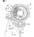
図1は、本発明の一実施の形態による縦型ALD装置を構成する炉の概略横断面図である。
図2は、本発明の一実施の形態による縦型ALD装置を構成する炉の概略縦断面図である。
図3は、本発明の一実施の形態による反応管内のバッファノズルの透視図である。
図4A、4Bは、プリ成膜にALD法と熱CVD法を採用した場合の、クリーニング、プリ成膜、成膜の各処理温度を比較した比較図である。
図5は、本発明の一実施の形態による縦型ALD装置の概略全体構成図である。
発明を実施するための好ましい形態
本発明の好ましい形態によれば、
基板を収容し、複数の反応ガスが供給され前記基板に所望の処理を行う空間を形成する反応容器と、
前記反応容器に開口し、前記反応容器内を排気するための排気口と、
前記反応容器へ少なくとも前記複数の反応ガスを供給するガス供給システムと、を有し、
前記ガス供給システムは、前記基板に所望の処理を行うことによって反応容器内に付着する付着物を除去するクリーニングガスを供給するクリーニングガス供給ユニットと、
前記クリーニングガスを供給して付着物を除去した後に反応容器内に残留するクリーニングガスに含まれた元素を除去することが可能な後処理用ガスを供給する後処理用ガス供給ユニットとを含み、
前記後処理用ガスは、前記基板に所望の処理を行なう際に用いる前記反応ガスの全てを含む第1の基板処理装置が提供される。
ここで、所望の処理とは、気相成長や表面反応による薄膜形成の他に、基板を加工する処理、例えば酸化膜の形成、拡散処理等が含まれる。
後処理用ガス供給ユニットから、クリーニングガスに含まれた元素を反応容器から除去することが可能な後処理用ガスを供給するようにしたので、反応容器内にプリ成膜し上記元素をトラップするものと比べて、クリーニングガスに含まれた元素を反応容器から除去することもできる。また、後処理用ガス供給ユニットは、基板に所望の処理を行なう際に用いる反応ガスの全てを後処理用ガスとして供給するので、クリーニングガスに含まれた元素と反応して揮発物を生成し、生成された揮発物を反応容器から有効に除去することも可能になる。また、後処理用ガス供給ユニットが、基板に所望の処理を行なう際に用いる反応ガスの全てを供給するガス供給手段で構成するものであれば、新たにガス供給系を増設する必要がなく構造の複雑化を回避できる。また、ガス供給系を増設した場合に生じるガス供給系からの異物発生を防止できる。
本発明の好ましい他の形態によれば、第1の基板処理装置において、前記後処理用ガス供給ユニットは、各反応ガスをそれぞれ独立して供給する専用の供給ノズルを有し、前記後処理用ガスとして前記反応ガスを供給する際には、前記各専用供給ノズルから各反応ガスを交互に供給する第2の基板処理装置が提供される。
第2の基板処理装置においては、後処理用ガス供給ユニットが、基板に所望の処理を行なう際に用いる複数の反応ガスをそれぞれ供給する各専用供給ノズルから、後処理用ガスとして各反応ガスを交互に供給することが可能なものであると、各専用供給ノズルから供給されるガスが、各専用供給ノズル内に残留したクリーニングガスに含まれた元素にそれぞれ有効に作用するので、各専用供給ノズル内に残留したクリーニングガスに含まれた元素を有効に除去することができる。この場合、基板に所望の処理を行なう方法と後処理を行なう方法との組合わせとしては、例えば、ALD法+ALD法、熱CVD法+ALD法の組合わせがある。
本発明の好ましい更に他の形態によれば、第2の基板処理装置において、前記後処理用ガス供給ユニットから供給される各反応ガスは、各専用供給ノズル内及び反応容器内に残留する元素を除去し、かつ反応容器内に所望の膜を形成させるガスである第3の基板処理装置が提供される。
第3の基板処理装置においては、後処理用ガス供給ユニットが、各専用供給ノズル内、及び反応容器内に残留する元素を除去するための各反応ガスを供給することが可能なものであると、各専用供給ノズル内、及び反応容器内に残留する元素を反応容器から有効に除去できる。また、後処理用ガス供給ユニットが、反応容器に所望の膜、すなわちプリ成膜を形成するための各反応ガスを供給することが可能なものであると、反応容器内に残留する元素をプリ成膜内に抑え込むことができる。したがって除去と抑え込みとの両面から残留元素を反応容器内の雰囲気から排除できるので、残留元素による成膜速度の低下を抑えることができる。また、各反応ガスを交互に供給することが可能なものであると、各専用供給ノズル内、及び反応容器内に形成する所望の膜は薄い膜で良く、スループットが向上する。
本発明の好ましい更に他の形態によれば、第3の基板処理装置において、前記各専用供給ノズルから供給する複数の反応ガスは、シリコンを含むガスと、プラズマ励起したアンモニアガスである第4の基板処理装置が提供される。
第4の基板処理装置においては、シリコンを含むガスは、シリコンを含むガスを供給する専用供給ノズル内に残留したクリーニングガスに含まれた元素を反応容器内の雰囲気から有効に排除できる。また、プラズマ励起したアンモニアガスは、アンモニアガスを供給する専用供給ノズル内に残留したクリーニングガスに含まれた元素を反応容器内の雰囲気から有効に排除できる。
本発明の好ましい更に他の形態によれば、第4の基板処理装置において、前記クリーニングガスはフッ素を含むガスであって、このフッ素を含むガスを、シリコンを含むガスを供給する専用供給ノズルから供給するものである第5の基板処理装置が提供される。
第5の基板処理装置においては、シリコンを含むガスはアンモニアガスよりも成膜しやすいので、シリコンを含むガスを供給する専用供給ノズルは、アンモニアガスを供給する専用供給ノズルと比べて、ノズル内に付着物がより多く付着しやすい。したがって、シリコンを含むガスを供給する専用供給ノズルから、クリーニングガスとしてフッ素を含むガスを供給すると、シリコンを含むガスを供給する専用供給ノズル内の付着物を除去して専用供給ノズル内を有効にクリーニングできる。
本発明の好ましい更に他の形態によれば、第4または第5の基板処理装置において、前記シリコンを含むガスは、DCS(SiH2Cl2)である第6の基板処理装置が提供される。
本発明の好ましい更に他の形態によれば、第5の基板処理装置において、前記フッ素を含むガスは、NF3,又はClF3である第7の基板処理装置が提供される。
本発明の好ましい更に他の形態によれば、
複数の反応ガスを交互に供給し、基板に薄膜を形成する基板処理装置であって、
反応容器と、
前記複数の反応ガスをそれぞれ専用に供給する複数の専用供給ノズルと、
クリーニング時は、前記複数の供給ノズルの1つからクリーニングガスを前記反応容器内に供給し、前記クリーニングガスの供給後、基板処理を行う前に、基板処理時に用いる前記複数の反応ガスの全てを、前記複数の専用供給ノズルからそれぞれ交互に前記反応容器内に供給するように制御する制御装置と、を備える第8の基板処理装置が提供される。
本発明の好ましい更に他の形態によれば、
反応容器内にクリーニングガスを供給し、前記反応容器内をクリーニングする工程の後、基板に処理を行なう際に用いる反応ガスの全てを反応容器に供給し、反応容器内に供給したクリーニングガスに含まれた元素を除去する工程を経た基板処理装置を用いて半導体装置を製造する第1の半導体装置の製造方法が提供される。
反応容器内をクリーニングする工程の後、基板に処理を行う際に用いる反応ガスの全てを反応容器に供給し、反応容器内に供給したクリーニングガスに含まれた元素を除去する工程を経た基板処理装置を用いて半導体装置を製造することによって、反応容器内に残留した前記元素を有効に除去でき、クリーニング工程後に行われる成膜工程時に、前記元素による成膜速度の低下が防止され、成膜量の安定した品質のよい半導体装置を製造することができる。
本発明の好ましい更に他の形態によれば、第1の半導体装置の製造方法において、前記反応ガスは、それぞれ専用の供給ノズルから反応容器内に供給され、前記クリーニングガスに含まれた元素を除去する工程は、各専用供給ノズルから各反応ガスを交互に供給する工程を含む第2の半導体装置の製造方法が提供される。
第2の半導体装置の製造方法においては、前記反応ガスは、それぞれ専用の供給ノズルから反応容器に供給され、前記クリーニングガスに含まれた元素を除去する工程は、各専用供給ノズルから各反応ガスを交互に供給する工程を含むので、反応容器内と各専用ノズル内に残留した前記元素を除去することができ、クリーニング工程後に行われる成膜工程時に、前記元素による成膜速度の低下がさらに防止され、さらに成膜量の安定した品質のよい半導体装置を製造することができる。
本発明の好ましい更に他の形態によれば、第2の半導体装置の製造方法において、前記クリーニングに含まれた元素を除去する工程は、各専用供給ノズル内及び反応容器内に残留する前記元素の除去と、反応容器内の構成物表面に所望の膜の形成とを含む第3の半導体装置の製造方法が提供される。
第3の半導体装置の製造方法においては、前記クリーニングガスに含まれた元素を除去する工程は、各専用供給ノズル内、および反応容器内に残留する前記元素を除去する工程と、反応容器の構成物表面に所望の膜を形成する工程とを含むので、反応容器内と各専用ノズル内に残留した前記元素を除去すると共に、反応容器内に形成した前記膜の中に前記元素を押さえ込むことができ、クリーニング工程後に行われる成膜工程時に、前記元素による成膜速度の低下がさらに防止され、さらに成膜量の安定した品質のよい半導体装置を製造することができる。
本発明の好ましい更に他の形態によれば、第1〜第3の半導体装置の製造方法において、前記複数の反応ガスはシリコンを含むガスと、アンモニアガスとである第4の半導体装置の製造方法が提供される。
第4の半導体装置の製造方法においては、好ましくは、アンモニアガスはプラズマ励起したアンモニアガスである。前記複数の反応ガスが、シリコンを含むガスと、プラズマ励起したアンモニアであると、各専用ノズル内に残留した前記元素を除去することができ、クリーニング工程後に行われる成膜工程時に、反応容器内と各専用ノズル内に残留した前記元素による成膜速度の低下がさらに防止され、さらに成膜量の安定した品質のよい半導体装置を製造することができる。
本発明の好ましい更に他の形態によれば、第4の半導体装置の製造方法において、前記クリーニングガスはフッ素を含むガスであって、前記クリーニングガスはシリコンを含むガスを供給する供給ノズルから反応容器内に供給する第5の半導体装置の製造方法が提供される。
第5の半導体装置の製造方法においては、前記クリーニングガスはフッ素を含むガスであって、前記クリーニングガスはシリコンを含むガスを供給する供給ノズルから反応容器内に供給するので、アンモニアガスに比べて成膜しやすいシリコンを含むガスを供給する専用ノズル内の付着物を有効に除去し、前記専用ノズル内を有効にクリーニングすることができ、異物による影響を抑制した半導体装置を製造することができる。
本発明の好ましい更に他の形態によれば、第4または第5の半導体装置の製造方法において、前記シリコンを含むガスは、DCS(SiH2Cl2)である第6の半導体装置の製造方法が提供される。
本発明の好ましい更に他の形態によれば、第5の半導体装置の製造方法において、前記フッ素を含むガスは、NF3、又はClF3である第7の半導体装置の製造方法が提供される。
次に、本発明の好ましい実施の形態を図面を参照して更に詳細に説明する。
図5は基板処理装置の一例を示す縦型ALD装置の概略構成図である。基板処理装置50の前面にはカセット授受ユニット49が設けられている。前記基板処理装置50の内部には、前記カセット授受ユニット49に対向してカセット棚51が設けられ、前記カセット授受ユニット49の上方に予備カセット棚52が設けられる。前記カセット授受ユニット49と前記カセット棚51との間にカセット搬送機53が設けられ、前記カセット棚51の後方に基板移載機54が設けられている。前記基板移載機54の後側にボートエレベータ55が設けられ、前記ボートエレベータ55の上方に縦型反応炉10が設けられている。
前記カセット授受ユニット49は基板搬送容器であるカセット57を2個載置可能なカセットステージ58、前記カセットステージ58の下方に基板姿勢整合機59を2組具備しており、外部搬送装置(図示せず)より搬送された前記カセット57が前記カセットステージ58に垂直姿勢(即ち、カセット57に収納されるウェーハ1が垂直姿勢の状態)で載置されると、前記基板姿勢整合機59が前記カセット57内のウェーハ等の基板(図示せず)のノッチやオリエンテーションフラットが同一位置となる様、ウェーハの姿勢を整合する。
前記カセットステージ58が90°回転し、前記カセット57を水平姿勢とすると共に前記カセット搬送機53により搬送可能な状態にする。
前記カセット搬送機53は前後方向に進退可能なロボットアーム60を具備し、前記ロボットアーム60は横行、及び昇降可能となっており、前記ロボットアーム60の進退、昇降、横行の協動により、前記カセットステージ58から前記カセット棚51、又は前記予備カセット棚52へ前記カセット57の搬送が行われる。
前記ボートエレベータ55から延びるアーム61にはシールキャップ17が設けられており、前記シールキャップ17に基板保持具であるボート2が載置される。前記ボート2はウェーハを水平姿勢で多段に保持するものであり、前記ボートエレベータ55により前記縦型反応炉10内に装入、引出しされる。
前記基板移載機54は回転・昇降可能に設けられ、進退可能なウェーハ保持部62を具備し、前記ウェーハ保持部62は複数枚のウェーハ保持プレート63を有し、ウェーハを複数枚一括、或は一枚ずつ保持可能となっている。
前記基板移載機54は前記カセット棚51のカセット57から下降状態の前記ボート2に複数枚一括、或は一枚ずつウェーハを移載する。
所定枚数のウェーハが前記ボート2に移載されると、前記縦型反応炉10に前記ボート2が装入され、ウェーハの処理がなされる。このウェーハ処理にはALD法が用いられ、処理に用いる複数種の反応ガスとしての原料ガスを1種類ずつ交互にウェーハ上に供給して1原子層単位で吸着・反応させ、これを繰り返すことにより処理している。
処理された基板は、上記した作動とは逆の作動により前記カセット棚51のカセット57に移載され、更に前記カセット搬送機53により前記カセット授受ユニット49に搬送され図示しない外部搬送装置により搬出される。
図2は実施の形態の縦型ALD装置の縦型反応炉10(以下、単に炉10という)の構成を示す。この炉10は、ヒータ14と、ヒータ14の内側に反応容器としての石英製円筒反応管11を備える。反応管11内に基板処理領域となる反応室12が形成される。反応管11の炉口部はシールキャップ17により気密に閉塞される。シールキャップ17に石英キャップ7を介してボート2が立設されて反応管11内に挿入される。ボート2は、天板3と底板4間に立設された複数本の支柱5を有し、これらの支柱5には多段に溝6が設けられる。ボート2には、これらの溝6に、処理されるウェーハ1が水平姿勢で多段に保持される。ボート2はボートエレベータ55(図5参照)によって昇降自在に支持され、反応11に対して出し入れできるようになっている。また、ボート2は図示しない回転機構によって回転軸19を中心に反応管11内で回転自在に設けられる。なお、18はシール用のOリングである。
反応管11にガス供給手段70が設けられ、ガス供給手段70から反応管11内へ複数の反応ガスを供給するようになっている。ガス供給手段70は、後述するクリーニングガス供給系と後処理用ガス供給系とを含む。また、反応管11に排気系として排気口16が設けられ、反応管11の内部を排気可能としている。
ガス供給手段70は、図2では便宜上、1系統のみが示されているが、実際には複数系統設けられていて、複数種類の原料ガス(ここでは2種類の原料ガス)を反応管11内に供給できるようになっている。複数種類の原料ガスのうちの一部のガスはプラズマにより活性化して供給されるガスであり、残りのガスはプラズマにより活性化しないで供給するガスである。例えば、基板上に形成する膜種がSiN膜の場合、原料ガスは、活性化を要するNH3ガスと、活性化を要しないDCSガスである。ここで示されているガス供給手段70は、プラズマにより活性化したNH3ガスを供給する第1のガス供給手段(NH3ガス供給手段)70Aである。第1のガス供給手段70Aは、反応管11の下部の一側に設けられたNH3ガス導入口20と、NH3ガス導入口20に接続され反応管11内に設けられている石英製のNH3用バッファノズル34とを備える。NH3用バッファノズル34は、反応管11内に導入されるNH3ガスの流量と流速とを全ウェーハにわたって均一化する。
NH3用バッファノズル34は、反応管11の管軸方向に延在され、反応管11の下部からボート2の頂部が位置する反応管頂部付近まで管内壁13に沿って設けられる。NH3用バッファノズル34は、管径が一様に細い通常のノズルと比べて比較的広いノズル空間を有し、ノズル空間を介して反応管11内にNH3ガスを噴出するようになっている。NH3用バッファノズル34の噴出孔(図示せず)は、多段に保持された多数枚のウェーハ1に対応するように、隣接するウェーハ1と同ピッチで多数設けられる。
また、このNH3用バッファノズル34は、内部にプラズマ発生用の一対のプラズマ電極27(図では、電極は重なって示されているため、一方のみが示されている)を有し、導入されるNH3ガスをプラズマで活性化している。一対のプラズマ電極27は、NH3用バッファノズル34内に設けられた一対の電極保護管25内にそれぞれ挿入される。一対の電極保護管25に挟まれたプラズマ生成領域33にプラズマ40が形成されるようになっている。
図1は、図2のI−I線矢視断面図である。第1のガス供給手段(NH3ガス供給手段)70Aと、第2のガス供給手段(DCSガス供給手段)70Bとが設けられて、反応管11内に2種類の原料ガスを個別に導入できるようになっている。第1のガス供給手段70Aと、第2のガス供給手段70Bとは制御装置100に接続され、制御装置100によって制御される。第1のガス供給手段70Aは、NH3ガス導入管22、NH3ガス導入管22を連結するNH3ガス導入口20、NH3ガス導入口20に連通するNH3用バッファノズル34から構成される。第2のガス供給手段70Bは、DCSガス導入管23、DCSガス導入管23を連結するDCSガス導入口21、DCSガス導入口21に連通するDCS用バッファノズル44から構成される。
第1のガス供給手段70Aは、専用供給ノズルとしてのNH3用バッファノズル34から、反応室12内に2種類の原料ガスのうちの1種であるNH3ガスの他に、後処理用ガスであるNH3ガス、又は不活性ガス例えばN2を供給するようになっている。NH3ガスは、成膜時、後処理時ともにプラズマで活性化して供給するように構成されている。
NH3用バッファノズル34は、NH3ガス導入口20に接続されたガス導入ノズル部28と、ガスを活性化するプラズマ生成ノズル部29とから構成される。ガス導入ノズル部28とプラズマ生成ノズル部29とは隔壁26を介して並設され、隔壁26に設けた連通口30を介して連通するようになっている。プラズマ生成ノズル部29には、プラズマ発生用の一対のプラズマ電極27が設けられ、導入されるガスをプラズマ40で活性化できるようになっている。活性化されたNH3ガス42はプラズマ生成ノズル部29に設けた噴出孔45から噴出されるようになっている。一対のプラズマ電極27は、プラズマ生成ノズル部29内に設けられた一対の電極保護管25内にそれぞれ挿入される。炉10の外部に電極保護管25から導出された一対のプラズマ電極27は、可変容量からなる整合器32を介して高周波電源31に接続される。
NH3ガス導入口20は、第1バルブ35、第2バルブ36を介してNH3ガス又は不活性ガスN2を供給する2分岐のガス導入管22に接続され、NH3用バッファノズル34にNH3又は不活性ガスを選択供給するようになっている。NH3ガス導入口20から導入されたガスは、NH3用バッファノズル34のガス導入ノズル部28に入り、連通口30を通ってプラズマ生成ノズル部29に供給される。ここでプラズマ電極27間に高周波電力を加えることによりプラズマ生成領域46にプラズマ40が発生し、このプラズマ40によりNH3ガスは活性化される。活性化されたNH3ガスはプラズマ生成ノズル部29の噴出孔45から反応室12内のウェーハ1上に噴出される。
このようにNH3用バッファノズル34は、その内部に比較的広いノズル空間を持っているので、ガスを励起した際に発生するラジカルがなるべく壁にぶつからず、またプラズマ生成領域46付近の圧力が低くなり、これにより発生したラジカルのライフタイムを確保して、NH3ラジカルをそのまま反応室(基板処理領域)12に輸送することができる。
第2のガス供給手段70Bは、専用供給ノズルとしてのDCS用バッファノズル44から、反応室12内に2種の原料ガスのうちの他の1種であるDCSガスの他に、クリーニングガスであるNF3ガス、後処理用ガスであるDCSガス、又は不活性ガスを供給するようになっている。DCSやNF3ガスはNH3と異なり、活性化しないで供給するようになっている。
DCS用バッファノズル44は、上述したNH3用バッファノズル34と異なり、プラズマ生成ノズル部を有さず、ガス導入ノズル部28に相当する部分だけを有して構成される。ガスはDCS用バッファノズル44の噴出孔47から反応室12内のウェーハ1上に噴出される。ガス導入口21は、第3バルブ37、第4バルブ38、第5バルブ39を介してDCS、NF3又は不活性ガスを供給する3分岐のガス導入管23に接続され、DCS用バッファノズル44にDCS、NF3又は不活性ガスを選択供給するようになっている。3分岐のガス導入管23のうち、DCSガスを供給するDCSガス導入管23Aは、反応管内圧力(以下、炉内圧力ともいう)をNH3ガスよりも高い圧力に短時間で昇圧することが好ましいため、第4バルブ38、第6バルブ43間に挟まれたDCSガスを溜めるバッファタンク41を有する。DCSガスを反応室12に供給する際には、予めDCSガスをバッファタンク41に溜め、反応室12の排気口16からの排気を例えば止めた状態で、バッファタンク41からバッファタンク41に溜めたDCSガスを反応室12に一気に供給することにより、反応室12内の複数のウェーハ1をDCSガスに晒すようにする。NF3ガス及び不活性ガスはバッファタンク41を通さないほうがよいので、これらを供給するガス導入管23B、23Cはバッファタンク41の下流につないである。
上述したガス導入管23B、DCSガス導入口21、及びDCS用バッファノズル44が、ウェーハ1に成膜を行なうことによって反応管11内に付着する付着物としての反応副生成物を除去するクリーニングガスを供給するクリーニングガス供給系71を構成する。また、第1のガス供給手段(NH3ガス供給手段)70A、及び第2のガス供給手段(DCSガス供給手段)70Bが、クリーニングガスを供給して反応副生成物を除去した後に反応管11内に残留するクリーニングガスに含まれたF成分を反応管11から除去することが可能な後処理用ガス供給系72を構成する。
図3は、反応管11内における2つのNH3用バッファノズル34、DCS用バッファノズル44を示す図であり、図1の右上に示す白抜き矢印Z方向から見た反応管11の透視図である。各バッファノズル34、44のガス噴出孔45、47は、バッファノズル34、44の上流から下流に向かって孔サイズを大きくしてある。これはバッファノズル34、44の上流から下流に向かってノズル空間の内部圧力が低くなっていくため、下流に向かって孔サイズを大きくすることによって、下流側でもガス噴出孔45、47から噴出される噴出量を確保し、上流から下流にわたって流量を均一に整えるためである。ガス噴出孔45、47は、前述したように、多段に保持された多数枚のウェーハ1に対応するように、隣接するウェーハ1と同ピッチで設けられる。
次に、上記のように構成される実施の形態の縦型ALD装置における作用を説明する。縦型ALD装置の反応管11内で成膜(成膜工程A)を繰り返すと、炉内部に反応副生成物が付着残留していく。これを除去するためにクリーニングを行なう(クリーニング工程B)。クリーニング後、炉内部に残留するクリーニングガスに含まれた元素を排除する後処理(後処理工程C)を行なう。後処理工程Cの後、成膜工程A、クリーニング工程Bを繰り返す。以下、各工程を個別に説明していく。なお、説明中に出てくる時間はオーバヘッドを除く値である。ここで、オーバヘッドとは、ボート1の反応管11内への挿入・取り出しに要する時間や、反応管内の真空引き・常圧復帰に要する時間等の時間であって、反応室内にガスを導入し処理を行っている時間を除く時間を示している。
成膜工程A
この工程はウェーハに所望の成膜処理を行なう本成膜工程である。ボートエレベータ55(図5参照)でシールキャップ17を介してボート2を下降させ、ボート2に多数枚のウェーハ1を保持し、ボートエレベータ55によりボート1を反応管11内に挿入する。シールキャップ17で反応管11の炉口を完全に密閉した後、反応管11内を排気口16から真空引きして排気する。反応管11内を所定温度、例えば400〜600℃に加熱し温度安定化をはかる。2つのバッファノズル34、44から原料ガスを反応室12内に供給しつつ排気口16より排出することにより、ウェーハ1表面に成膜処理する。
前述したようにALD装置では、DCSガスとNH3プラズマとはそれぞれ専用のDCS用ノズルとNH3用ノズルとから交互に供給されるように構成される。特に、積層した基板を一度に大量に処理する縦型ALD装置では、積層された各基板に均一にガスを輸送するために、DCS用ノズル及びNH3用ノズルは、細管で構成された通常のノズルではなく、ノズル空間の大きなバッファノズルで構成することがある。また、DCS用バッファノズルと異なり、NH3用バッファノズル内には、プラズマ電極が設けられたプラズマ生成領域と、NH3ガスが導入されるプラズマ非生成領域とを備え、プラズマ非生成領域に導入されたNH3ガスをプラズマ生成領域でプラズマにより活性化できるようになっている。そして、各バッファノズル内にSiN膜が成膜しにくいように、DCS用バッファノズルからDCSガスを供給する時はNH3用バッファノズルからN2などの不活性ガスを流し、NH3用バッファノズルからNH3プラズマを供給する時はDCS用バッファノズルからN2などの不活性ガスを流している。
この成膜処理は、2種類の反応ガスDCSとNH3とを用いたALD成膜処理で行われ、次の▲1▼〜▲4▼のステップから構成される。
▲1▼NH3用バッファノズル34のプラズマ電極27間への高周波電力印加はオフにしておく。また、NH3用バッファノズル34内へのDCSガスの混入を防止するため、第2バルブ36を開いて、少量のN2ガスを流しておく。第4バルブ38を開けて予めバッファタンク41に溜めたDCSガスをDCS用バッファノズル44に供給し、その噴出孔47から反応室12に噴射する。噴射するDCS流量は例えば0.5slmであり、炉内圧力は排気口16の排気を止めて例えば266〜931Paとする。DCSガスにウェーハ1が晒されることで、ウェーハ1上にDCS原料が吸着される。
▲2▼第4バルブ38を閉めDCSガスの供給を止める。第6バルブ43を開いてバッファタンク41へのDCSガス溜めを開始する。ついで、排気口16を開けると共に、第5バルブ39を開けて不活性ガスであるN2ガスをDCS用バッファノズル(第2バッファノズル)44から反応管11内に導入し、DCS用バッファノズル44及び反応管11内をN2パージしてDCS雰囲気をDCS用バッファノズル44及び反応管11内から除去する。なお、N2パージに代えて真空引きでDCS雰囲気を除去してもよい。
▲3▼DCS用バッファノズル44内へのNH3ラジカル42の混入を防止するため、第5バルブ39を開いて、少量のN2ガスを流しておく。プラズマ電極27間に高周波電力を印加するとともに、第1バルブ35を開けてNH3ガスをNH3用バッファノズル(第1バッファノズル)34に供給する。NH3ガスはガス導入ノズル部28から連通孔30を通ってプラズマ生成ノズル部29に導入され、プラズマ電極27間で発生したプラズマ40により活性化される。活性化されたNH3ラジカル42は、噴射孔45から反応室12に噴射される。噴射されるNH3ガス流量は例えば3.0〜4.5slmであり、炉内圧力は排気口16のコンダクタンス制御によりDCSガス導入のときより低い40〜60Paとする。活性化したNH3ガスにウェーハ1が晒されることで、ウェーハ1上に吸着されていたDCS原料とNH3原料とが反応してウェーハ1上に1原子層だけSiN膜が成膜される。
▲4▼第1バルブ35を閉じてNH3ガスの供給を止めるとともに、プラズマ電極27間への高周波電力印加はオフにする。排気口16は開けたままとして、第2バルブ36を開けて不活性ガスであるN2ガスをNH3用バッファノズル34に導入し、ガス導入ノズル部28からプラズマ生成ノズル部29を通して反応管11内に導入し、NH3用バッファノズル34及び反応管11内をN2パージしてNH3雰囲気をNH3用バッファノズル34及び反応管11から除去する。なお、N2パージに代えて真空引きでNH3雰囲気を除去してもよい。
再び▲1▼へ戻って、▲1▼〜▲4▼のステップを所望の回数だけ繰り返す。ステップ▲1▼〜▲4▼を1サイクルとして、1サイクルで一定の膜厚が成膜されていく。膜厚はサイクル数で制御する。成膜時間は温度、膜厚に依存するが、例えば成膜温度550℃、膜厚300Åとすれば100min程度である。なお、上述したステップでは、先にDCSガスを供給し、後からNH3プラズマを供給するようにしたが、供給順序を逆にして、先にNH3プラズマを供給し、後からDCSガスを供給するようにしてもよい。
このようにして成膜を完了した後は、反応管11内を不活性ガスN2に置換して常圧に復帰させ、ボート2を下降させ、ボート2から成膜完了後のウェーハ1を払い出す。
しかし、上述したように一方のバッファノズルから原料ガスを流す時に他方のバッファノズルから不活性ガスを流すようにしても、拡散現象によってバッファノズル間でガスがある程度混入するのは避けられない。原料ガスがプラズマ励起されるNH3用バッファノズルでは、DCSガスが混入すると、ノズルが異物発生源となる。ノズルが異物発生源となるのは次の理由による。
▲1▼プラズマ放電時にNH3用バッファノズルのプラズマ生成領域にDCSガスが混入していると、DCSとNH3プラズマとが劇的に反応し、ポリマ等を形成してNH3用バッファノズル内部に膜が付着する。これが異物発生源となる。
▲2▼DCSとNH3プラズマとの反応により、プラズマ生成領域部に膜が付着していくが、膜が厚く付着してしまうと、プラズマ放電時に、付着した膜にNH3ラジカルが激しく衝突し、膜にダメージを与え膜剥がれを生じることがある。これも異物発生源になる。
そこで、複数のガスを交互に供給する複数の専用バッファノズルを使用している縦型ALD装置では、バッファノズル内の成膜を除去するために、後述するクリーニング工程Bでバッファノズル内にもクリーニングガスが入り込むようにする必要ある。
クリーニング工程B
ボート2にウェーハ1を保持しない状態で、ボートエレベータ55によりボート1を反応管11内に挿入する。シールキャップ17で反応管11の炉口を完全に密閉した後、反応管11内を排気口16から真空引きして排気する。反応管内温度を例えば約610℃にする。第3バルブ37を開けてクリーニングガスとなるNF3ガスをDCS用バッファノズル44から反応室12内に噴射する。噴射するNF3ガス流量は例えば0.25〜1.5slmである。このとき反応管11の内部の真空排気はそのまま継続され、反応管11の内部の圧力は予め定めた圧力になるように、真空排気量が制御される。炉内の熱でNF3分子が活性化される。これにより炉内接ガス部となるDCS用バッファノズル44の内壁面、反応管11の内壁面、炉口部付近8の炉低温部、又はその他の接ガス部に付着した反応副生成物がエッチングされる。また、NH3用バッファノズル34内にもNF3ガスが入ってプラズマ生成ノズル部29内の反応副生成物がエッチングされる。エッチングされた反応副生成物は、排気口16から排出される。クリーニング時間は累積膜厚に依存するが、例えば0.75μm累積時は2h程度である。
ここで、NH3用バッファノズル34のガス導入ノズル部28内はプラズマ生成領域46以外のプラズマ非生成領域48であり、ガス導入ノズル部28内にNF3ガスが入ってノズル部内壁面にF成分が吸着、結合して残留すると、NH3プラズマが存在しないのでF成分を除去できない。そのため、クリーニング時は、ガス導入ノズル部28から微量の窒素N2を流し、ガス導入ノズル部28内にクリーニングガスが混入しないようにしている。ここで、窒素N2を流す量を微量としているのは、次の理由による。プラズマ生成ノズル部29内には、DCSガスの拡散より、多少の反応副生成物が付着していると考えられるので、前述したように、プラズマ生成ノズル部29内にクリーニングガスを入れて反応副生成物を除去する必要がある。したがって窒素N2の流す量を多くすると、クリーニングガスがプラズマ生成ノズル部29内に入らなくなって、反応副生成物を除去できなくなり、これを防ぐためである。
また、実施の形態では、クリーニングガスをNH3ガスを供給するNH3用バッファノズル34ではなく、DCSガスを供給するDCS用バッファノズル44から流している。これは次の3つの理由による。
▲1▼DCSガスのみでも成膜するので、NH3用バッファノズル34内に付着する反応副生成物の膜より、DCS用バッファノズル44内に付着する反応副生成物の膜の方が、より厚い膜になっていると考えられる。したがって、これを有効に除去する必要がある。
▲2▼クリーニングを実施した後に成膜を行なうと成膜速度が低下する。これは成膜ガスが残留F成分に影響されて成膜が阻害されるからである。反応ガスがDCS+NH3プラズマ系の場合、残留したFとの反応は、DCSガスよりもNH3プラズマの方が、Fとの反応確率が高く、Fによる影響を受けやすい。このためNH3用バッファノズル34からNF3ガスを流した時の方が、DCS用バッファノズル44からNF3ガスを流したときよりも、その後の成膜速度低下が大きくなる。したがって、Fによる影響を受けにくい方から流す方が好ましい。
▲3▼NH3用バッファノズル内にクリーニングガスが入り込むようにすると、F成分がNH3用バッファノズル内のノズル内壁面に吸着、結合する。NH3はプラズマ励起を行わないとフッ素Fと反応しないため、NH3用バッファノズル34からNF3ガスを供給した場合、プラズマ生成領域46以外のプラズマ非生成領域48でF成分が吸着、結合して残留すると、このF成分が除去できず、ウェーハ処理開始からしばらくの間、Fを反応室12内に供給し続けることになり、しばらくは成膜速度が安定しないということになる。これを回避する必要がある。
後処理工程C
後処理工程は、クリーニング工程の後に行なう工程であり、各バッファノズル34、44内、及び反応室12内に残留する元素Fを反応管11から除去する除去工程と、各バッファノズル34、44内、及び反応管11内の構成物表面に所望の膜を形成するプリ成膜工程とが含まれる。2つの除去工程及びプリ成膜工程は、別個の工程とすることもできるが、ALD法を用いると両工程を1つの工程で実施することができる。ALD法を用いた1つの工程で実現する場合のプリ成膜内容は、基本的には前述した成膜工程Aと同じであり、成膜工程Aと異なる点は、処理時間が例えば13min程度と短い点であり、この処理時間で例えば40サイクル程度の成膜処理を行うことで、後処理後に行われるウェーハ成膜の膜厚を安定させることができる。
後処理工程として、プラズマによって励起したNH3ラジカルとDCSガスとを交互に供給するALD法で後処理工程を実施すると、炉内の各接ガス部のF成分は次のように除去される。
▲1▼NH3用バッファノズル
NH3用バッファノズル34にNH3ガスが後処理用ガスとして供給される。すると、このNH3はプラズマにより活性化されるので、NH3用バッファノズル34のプラズマ生成ノズル部29内の壁面に吸着、結合して残留しているF成分は、活性化によりNH3から電離されたH原子と反応して、NH3用バッファノズル34内から排出されやすいHFガスとなる。HFガスはNH3用バッファノズル34から反応室12を通って反応管11の排気口16から排出される。また、プリ成膜時、意図的にNH3用バッNH3ファノズル34内にプリ成膜であるSiN膜を形成していないが、DCSガス供給時のガスの拡散作用により、NH3用バッファノズル34内に多少のDCSガスが流入するので、NH3用バッファノズル34内に多少のプリ成膜SiNが形成されると考えられる。したがってNH3用バッファノズル34内の壁面に吸着、結合して残留しているF成分は、これらの膜原料との反応や、膜の下への封じ込めにより、反応管内雰囲気から排除される。なお、NH3ラジカルが生成されないガス導入ノズル部28については、クリーニング時に、微量の窒素N2を流してF成分が混入しないようにしているので、特にNH3ラジカルによる除去とプリ成膜による抑え込みとを要さない。
▲2▼DCS用バッファノズル
DCS用バッファノズル44にDCSガスが後処理用ガスとして供給される。すると、このDCS(SiH2Cl2)ガスはSi−F結合を作りやすいので、DCS用バッファノズル44内の壁面に吸着、結合して残留しているF成分は、DCSガスと反応してSiF(フッ化シリコン)ガスとなる。このSiFガスはDCS用バッファノズル44から反応室12を通って反応管11の排気口16から排出される。また、プリ成膜時、意図的にDCS用バッファノズル44内にプリ成膜であるSiN膜を形成していないが、NH3ラジカル供給時のガスの拡散作用により、DCS用バッファノズル44内に多少のDCSガスが流入するのでDCS用バッファノズル44内に多少のプリ成膜SiNが形成されると考えられる。したがって、DCS用バッファノズル44内の壁面に吸着、結合して残留しているF成分は、これらの膜原料との反応や、膜の下への封じ込めにより反応管内雰囲気から排除される。
▲3▼炉低温部
炉口部付近8の炉低温部に吸着、結合して残留しているF成分にも、NH3用バッファノズル34から反応室12内に供給されるNH3ラジカルはFとの反応確率が高いため、特に有効に作用し、F成分はHFになって反応管11から排出される。また、各バッファノズル34、44からNH3ラジカルとDCSガスとが交互に反応管11内に供給されることで炉低温部に形成されるプリ成膜によっても、壁面に吸着、結合して残留しているF成分を膜の下に封じ込めて、反応管11内の雰囲気から排除される。
▲4▼上記以外の部分
上記以外の炉内の接ガス部は、プリ成膜の形成、DCSガス又はNH3ラジカルとの反応によるF成分の揮発化によって、壁面に吸着、結合して残留しているF成分を抑えこみ、かつ除去させることができる。
以上述べた▲1▼〜▲4▼の除去効果によって、炉内の各接ガス部のF成分は有効に除去されるので、クリーニング直後であっても、基板上への成膜時にF成分が脱離してきて成膜を阻害することがなくなり、成膜速度の低下を有効に抑えることができる。
上述したように実施の形態によれば、後処理工程となるプリ成膜を行なうに際し、熱CVD法ではなくALD法を採用し、その際、本成膜で用いる原料ガスの全てを後処理用ガスとして供給しているので、NH3ラジカルとDCSによるF元素の炉からの除去と、プリ成膜によるF元素の炉内でのトラップとの両面から、F元素を反応管内の雰囲気から有効に排除することができる。
また、熱CVD法によるプリ成膜の場合、F成分のトラップには厚い膜が必要である。すなわち、熱CVD法の場合、炉口部付近8の低温部は、炉の他の接ガス部分に比べて成膜速度が低いので、低温部にあわせてF成分をトラップするためのプリ成膜を付けると、成膜処理時間が長くなって他の接ガス部分の膜厚が厚くなる。また、熱CVD法では、プラズマを使用していないため、NH3プラズマによる残留F成分の反応室12外への排出機能がない。それゆえ、多量の残留F成分をプリ成膜の下に封じ込める必要があり、結果的に、厚いプリ成膜が必要となる。これに対して実施の形態のようにALD法によるプリ成膜の場合、F成分のトラップには薄い膜でよい。すなわち、ALD法の場合、NH3プラズマが、低温部付近の残留F成分を有効に取り去るので、薄いプリ成膜で済む。また、プリ成膜が薄い場合、その後の基板処理によって、反応管内壁面に付着する反応副生成物が、膜剥がれを起こし始めるまでの期間が長くなり、クリーニングの回数を減少させることができる。
したがって図4A、4Bに示すように、プリ成膜を行なうに際して、従来のように熱CVD法を用いると厚い膜厚が必要となり、成膜速度を稼ぐために、処理温度を上げる必要がある(図4B)。これに対して実施の形態では、ALD法を用いるので、NH3プラズマとDCSガスによる残留F成分の除去効果によるプリ成膜の薄膜化が実現できるので、プリ成膜温度を本成膜の成膜温度と同じにすることができ、スループットを向上できる(図4A)。
また、本実施の形態では、後処理用ガスを供給する後処理用ガス供給系として、各専用供給ノズルであるNH3用バッファノズルとDCSガスバッファノズルとをそのまま利用しており、専用供給ノズルとは別に熱CVD成膜用ノズルを増設する必要が生じないので、反応管の構造が複雑になることも、コストアップにつながることもない。また、熱CVD成膜用ノズルを増設しないので、CVD成膜用ノズル内における成膜による異物発生の問題も生じない。
以上に記述した成膜工程、クリーニング工程、後処理工程を経た基板処理装置を用いて半導体装置を製造すれば、反応室内に残留したクリーニングガスに含まれる元素による影響の少ない半導体装置を製造することができる。
またDCSとプラズマ励起NH3との原料ガスを用いてSiNを成膜したが、ガス種はこれに限らない。例えばSiN膜では、Si2Cl6(ヘキサクロロジシラン:HCD)とNH3(プラズマ励起してもプラズマ励起しなくてもよい)との原料ガスを用いて成膜することも可能である。
また、実施の形態ではクリーニングガスとしてNF3を用いたが、これに限らず、ClF3などの他のF(フッ素)を含むエッチングガスを用いてもよい。
また、実施の形態では、本成膜と後処理とを共にALD法で行なっているが、これに限定されず、例えば本成膜を熱CVD法で行い、後処理のみをALD法で行ってもよい。また、実施の形態ではバッチ式の縦型ALD装置に適用したが、枚葉式のALD装置にも適用できる。
また、実施の形態では、通常のノズルと比べて空間容積の大きな2つのバッファノズルを備え、一方のバッファノズル内でガスをプラズマ励起する構造のものについて説明したが、これに限定されない。例えば、後処理工程の処理時間は増大するが、バッファノズルの外でプラズマ励起するもの、あるいは通常の細管ノズルを備えノズル外でプラズマ励起する構造のものにも適用可能である。
明細書、特許請求の範囲、図面および要約書を含む2002年11月11日提出に日本国特許出願2002−327193号の開示内容全体は、そのまま引用してここに組み込まれる。FIG. 1 is a schematic cross-sectional view of a furnace constituting a vertical ALD apparatus according to an embodiment of the present invention.
FIG. 2 is a schematic longitudinal sectional view of a furnace constituting the vertical ALD apparatus according to the embodiment of the present invention.
FIG. 3 is a perspective view of a buffer nozzle in a reaction tube according to an embodiment of the present invention.
4A and 4B are comparative diagrams comparing the processing temperatures of cleaning, pre-film formation, and film formation when the ALD method and the thermal CVD method are employed for the pre-film formation.
FIG. 5 is a schematic overall configuration diagram of a vertical ALD apparatus according to an embodiment of the present invention.
Preferred form for carrying out the invention
According to a preferred form of the invention,
A reaction container that contains a substrate and is supplied with a plurality of reaction gases to form a space for performing desired processing on the substrate;
An opening for opening the reaction vessel and exhausting the reaction vessel;
A gas supply system for supplying at least the plurality of reaction gases to the reaction vessel,
The gas supply system includes a cleaning gas supply unit that supplies a cleaning gas that removes deposits adhering to the reaction container by performing a desired process on the substrate;
A post-treatment gas supply unit for supplying a post-treatment gas capable of removing an element contained in the cleaning gas remaining in the reaction vessel after supplying the cleaning gas and removing deposits,
A first substrate processing apparatus is provided in which the post-processing gas contains all of the reaction gas used when a desired process is performed on the substrate.
Here, the desired processing includes processing for processing a substrate, for example, formation of an oxide film, diffusion processing, and the like in addition to thin film formation by vapor phase growth or surface reaction.
Since an aftertreatment gas capable of removing the elements contained in the cleaning gas from the reaction vessel is supplied from the aftertreatment gas supply unit, a pre-film is formed in the reaction vessel and the above elements are trapped. Compared to the above, the elements contained in the cleaning gas can be removed from the reaction vessel. Further, the post-processing gas supply unit supplies all of the reaction gas used when performing desired processing on the substrate as the post-processing gas, and thus reacts with the elements contained in the cleaning gas to generate volatiles. It is also possible to effectively remove the generated volatiles from the reaction vessel. Further, if the post-processing gas supply unit is constituted by gas supply means for supplying all of the reaction gas used when performing desired processing on the substrate, there is no need to newly add a gas supply system. Can be avoided. Further, it is possible to prevent the generation of foreign matter from the gas supply system that occurs when the gas supply system is expanded.
According to another preferred embodiment of the present invention, in the first substrate processing apparatus, the post-processing gas supply unit has a dedicated supply nozzle for supplying each reaction gas independently, and the post-processing gas supply unit When supplying the reaction gas as a gas, a second substrate processing apparatus is provided that alternately supplies each reaction gas from each dedicated supply nozzle.
In the second substrate processing apparatus, the post-processing gas supply unit supplies each reaction gas as a post-processing gas from each dedicated supply nozzle that supplies each of a plurality of reaction gases used when performing desired processing on the substrate. If the gas can be supplied alternately, the gas supplied from each dedicated supply nozzle effectively acts on the elements contained in the cleaning gas remaining in each dedicated supply nozzle. Elements contained in the cleaning gas remaining in the nozzle can be effectively removed. In this case, as a combination of a method for performing desired processing on the substrate and a method for performing post-processing, for example, there are combinations of ALD method + ALD method and thermal CVD method + ALD method.
According to still another preferred embodiment of the present invention, in the second substrate processing apparatus, each reaction gas supplied from the post-processing gas supply unit contains elements remaining in each dedicated supply nozzle and in the reaction vessel. A third substrate processing apparatus is provided which is a gas for removing and forming a desired film in the reaction vessel.
In the third substrate processing apparatus, the post-processing gas supply unit can supply each reaction gas for removing elements remaining in each dedicated supply nozzle and in the reaction vessel. In addition, the elements remaining in the dedicated supply nozzles and in the reaction vessel can be effectively removed from the reaction vessel. Further, if the post-treatment gas supply unit is capable of supplying each reaction gas for forming a desired film, that is, a pre-film formation, to the reaction container, the elements remaining in the reaction container are pre-treated. It can be suppressed in the film formation. Therefore, since the residual element can be excluded from the atmosphere in the reaction vessel from both sides of removal and suppression, it is possible to suppress a decrease in the film formation rate due to the residual element. Further, if each reaction gas can be alternately supplied, the desired film formed in each dedicated supply nozzle and in the reaction vessel may be a thin film, and the throughput is improved.
According to still another preferred embodiment of the present invention, in the third substrate processing apparatus, the plurality of reaction gases supplied from the dedicated supply nozzles are a gas containing silicon and an ammonia gas excited by plasma. A substrate processing apparatus is provided.
In the fourth substrate processing apparatus, the gas containing silicon can effectively exclude the elements contained in the cleaning gas remaining in the dedicated supply nozzle for supplying the gas containing silicon from the atmosphere in the reaction vessel. The plasma-excited ammonia gas can effectively exclude elements contained in the cleaning gas remaining in the dedicated supply nozzle for supplying ammonia gas from the atmosphere in the reaction vessel.
According to still another preferred aspect of the present invention, in the fourth substrate processing apparatus, the cleaning gas is a gas containing fluorine, and the fluorine-containing gas is supplied from a dedicated supply nozzle for supplying a gas containing silicon. A fifth substrate processing apparatus to be supplied is provided.
In the fifth substrate processing apparatus, since the gas containing silicon is easier to form a film than the ammonia gas, the dedicated supply nozzle for supplying the gas containing silicon is located in the nozzle as compared with the dedicated supply nozzle for supplying the ammonia gas. More deposits are likely to adhere to the surface. Therefore, if a gas containing fluorine is supplied as a cleaning gas from a dedicated supply nozzle that supplies a gas containing silicon, deposits in the dedicated supply nozzle that supplies the gas containing silicon are removed, and the inside of the dedicated supply nozzle becomes effective. Can be cleaned.
According to still another preferred embodiment of the present invention, in the fourth or fifth substrate processing apparatus, the gas containing silicon is DCS (SiH2 Cl2 ) Is provided.
According to still another preferred embodiment of the present invention, in the fifth substrate processing apparatus, the gas containing fluorine is NF.3 Or ClF3 A seventh substrate processing apparatus is provided.
According to still another preferred aspect of the present invention,
A substrate processing apparatus for alternately supplying a plurality of reaction gases to form a thin film on a substrate,
A reaction vessel;
A plurality of dedicated supply nozzles for supplying the plurality of reaction gases exclusively;
During cleaning, a cleaning gas is supplied into the reaction vessel from one of the plurality of supply nozzles, and after the cleaning gas is supplied, before performing substrate processing, all of the plurality of reaction gases used during substrate processing are removed. There is provided an eighth substrate processing apparatus comprising: a control device that controls to alternately supply the plurality of dedicated supply nozzles into the reaction vessel.
According to still another preferred aspect of the present invention,
After the step of supplying a cleaning gas into the reaction vessel and cleaning the inside of the reaction vessel, all of the reaction gas used when processing the substrate is supplied to the reaction vessel and is included in the cleaning gas supplied into the reaction vessel. A first method for manufacturing a semiconductor device is provided, in which a semiconductor device is manufactured using a substrate processing apparatus that has undergone a step of removing the element.
After the step of cleaning the inside of the reaction vessel, all of the reaction gas used when processing the substrate is supplied to the reaction vessel, and the substrate processing is performed after the step of removing the elements contained in the cleaning gas supplied into the reaction vessel. By manufacturing the semiconductor device using the apparatus, the element remaining in the reaction vessel can be effectively removed, and the film formation speed is prevented from being lowered by the element during the film formation process performed after the cleaning process. A semiconductor device with a stable quantity and a good quality can be manufactured.
According to still another preferred aspect of the present invention, in the first method for manufacturing a semiconductor device, the reaction gas is supplied into a reaction vessel from a dedicated supply nozzle, and an element contained in the cleaning gas is removed. The step of performing a second semiconductor device manufacturing method includes a step of alternately supplying each reaction gas from each dedicated supply nozzle.
In the second method for manufacturing a semiconductor device, the reaction gas is supplied to the reaction vessel from a dedicated supply nozzle, and the step of removing the element contained in the cleaning gas is performed from each dedicated supply nozzle. The element remaining in the reaction vessel and each dedicated nozzle can be removed, and the film formation rate is further reduced by the element during the film formation process performed after the cleaning process. Thus, it is possible to manufacture a high-quality semiconductor device that is prevented and has a stable film formation amount.
According to still another preferred aspect of the present invention, in the second method for manufacturing a semiconductor device, the step of removing the element included in the cleaning is performed by removing the element remaining in each dedicated supply nozzle and in the reaction vessel. A third method for manufacturing a semiconductor device is provided that includes removal and formation of a desired film on the surface of a component in the reaction vessel.
In the third method of manufacturing a semiconductor device, the step of removing the element contained in the cleaning gas includes the step of removing the element remaining in each dedicated supply nozzle and in the reaction vessel, and the configuration of the reaction vessel. Forming a desired film on the surface of the object, so that the element remaining in the reaction vessel and each dedicated nozzle can be removed and the element can be pressed into the film formed in the reaction vessel. In addition, during the film-forming process performed after the cleaning process, a decrease in the film-forming speed due to the elements can be further prevented, and a semiconductor device with a stable film formation amount and high quality can be manufactured.
According to still another preferred embodiment of the present invention, in the first to third semiconductor device manufacturing methods, the plurality of reaction gases are a gas containing silicon and ammonia gas. Is provided.
In the fourth method for fabricating a semiconductor device, preferably, the ammonia gas is plasma-excited ammonia gas. When the plurality of reaction gases are silicon-containing gas and plasma-excited ammonia, the element remaining in each dedicated nozzle can be removed, and the film is formed in the reaction vessel during the film-forming process performed after the cleaning process. Further, it is possible to further prevent a decrease in the film formation rate due to the elements remaining in the dedicated nozzles, and to manufacture a semiconductor device with a high quality and a stable film formation amount.
According to still another preferred embodiment of the present invention, in the fourth method of manufacturing a semiconductor device, the cleaning gas is a gas containing fluorine, and the cleaning gas is a reaction vessel from a supply nozzle that supplies a gas containing silicon. A fifth semiconductor device manufacturing method to be supplied inside is provided.
In the fifth method of manufacturing a semiconductor device, the cleaning gas is a gas containing fluorine, and the cleaning gas is supplied into the reaction vessel from a supply nozzle that supplies a gas containing silicon. It is possible to effectively remove deposits in a dedicated nozzle that supplies a gas containing silicon that is easy to form a film, effectively clean the inside of the dedicated nozzle, and manufacture a semiconductor device that suppresses the influence of foreign matter. .
According to still another preferred embodiment of the present invention, in the fourth or fifth method for fabricating a semiconductor device, the gas containing silicon is DCS (SiH2 Cl2 ) Is provided. A sixth semiconductor device manufacturing method is provided.
According to still another preferred embodiment of the present invention, in the fifth method for manufacturing a semiconductor device, the gas containing fluorine is NF.3 Or ClF3 A seventh method for manufacturing a semiconductor device is provided.
Next, preferred embodiments of the present invention will be described in more detail with reference to the drawings.
FIG. 5 is a schematic configuration diagram of a vertical ALD apparatus showing an example of a substrate processing apparatus. A
The
The
The
A
The
The
When a predetermined number of wafers are transferred to the
The processed substrate is transferred to the
FIG. 2 shows a configuration of a vertical reactor 10 (hereinafter simply referred to as a furnace 10) of the vertical ALD apparatus of the embodiment. The
A gas supply means 70 is provided in the
For the sake of convenience, FIG. 2 shows only one system of the gas supply means 70, but actually a plurality of systems are provided, and a plurality of types of source gases (here, two types of source gases) are supplied into the
NH3 The
This NH3 The
1 is a cross-sectional view taken along the line II of FIG. First gas supply means (NH3 Gas supply means) 70A and second gas supply means (DCS gas supply means) 70B are provided so that two kinds of source gases can be individually introduced into the
The first gas supply means 70A has NH as a dedicated supply nozzle.3 NH, which is one of two types of source gases, from the
NH3 Buffer nozzle 34 for NH3 A gas
NH3 The
In this way NH3 Since the
The second gas supply means 70B is a cleaning gas in addition to the DCS gas which is the other one of the two kinds of source gases in the
The
The above-described
FIG. 3 shows two NHs in the
Next, the operation of the vertical ALD apparatus according to the embodiment configured as described above will be described. When film formation (film formation process A) is repeated in the
Film formation process A
This step is a main film forming step for performing a desired film forming process on the wafer. The
As described above, in the ALD apparatus, DCS gas and NH3 Plasma is a dedicated DCS nozzle and NH3 It is comprised so that it may be alternately supplied from the nozzle for use. In particular, in a vertical ALD apparatus that processes a large number of stacked substrates at a time, a DCS nozzle and NH are used to transport gas uniformly to each stacked substrate.3 The nozzle for use may be constituted by a buffer nozzle having a large nozzle space, instead of a normal nozzle constituted by a thin tube. Also, unlike DCS buffer nozzles, NH3 In the buffer nozzle, a plasma generation region provided with a plasma electrode, and NH3 A non-plasma generation region into which gas is introduced, and NH introduced into the non-plasma generation region3 The gas can be activated by plasma in the plasma generation region. When supplying the DCS gas from the DCS buffer nozzle, it is difficult to form a SiN film in each buffer nozzle.3 N for buffer nozzle2 Inert gas such as NH3 NH for buffer nozzle3 When supplying plasma, N from the buffer nozzle for DCS2 An inert gas such as
This film forming process includes two kinds of reactive gases DCS and NH.3 And is composed of the following steps (1) to (4).
▲ 1 ▼ NH3 Application of high frequency power between the
(2) Close the
(3) NH into the
(4) Close the
Returning to (1) again, steps (1) to (4) are repeated as many times as desired. Steps {circle around (1)} to {circle around (4)} are taken as one cycle, and a constant film thickness is formed in one cycle. The film thickness is controlled by the number of cycles. Although the film formation time depends on the temperature and the film thickness, for example, if the film formation temperature is 550 ° C. and the film thickness is 300 mm, it is about 100 min. In the above-described steps, the DCS gas is supplied first, and NH3 Plasma was supplied, but the order of supply was reversed and NH3 Plasma may be supplied and DCS gas may be supplied later.
After the film formation is completed in this way, the inside of the
However, as described above, even if the inert gas is allowed to flow from the other buffer nozzle when the source gas is allowed to flow from one buffer nozzle, it is inevitable that the gas is mixed to some extent between the buffer nozzles due to the diffusion phenomenon. NH where source gas is plasma-excited3 In the buffer nozzle, when the DCS gas is mixed, the nozzle becomes a foreign matter generation source. The nozzle is a foreign matter generation source for the following reason.
(1) NH during plasma discharge3 If DCS gas is mixed in the plasma generation area of the buffer nozzle for the DCS, DCS and NH3 NH3 reacts dramatically with plasma, forms polymers, etc.3 A film adheres to the inside of the buffer nozzle. This becomes a foreign matter generation source.
(2) DCS and NH3 The film adheres to the plasma generation region due to the reaction with the plasma, but if the film adheres thickly, the NH film adheres to the deposited film during plasma discharge.3 Radicals can collide violently, damaging the film and causing film peeling. This also becomes a foreign matter generation source.
Therefore, in a vertical ALD apparatus that uses a plurality of dedicated buffer nozzles that alternately supply a plurality of gases, in order to remove film formation in the buffer nozzles, the buffer nozzles are also cleaned in a cleaning step B described later. It is necessary to allow gas to enter.
Cleaning process B
The
Where NH3 The gas
In the embodiment, the cleaning gas is NH.3 NH supplying gas3 It flows from the
(1) Since only DCS gas is used for film formation, NH3 It is considered that the reaction by-product film deposited in the
{Circle around (2)} When the film is formed after the cleaning is performed, the film forming speed decreases. This is because the deposition gas is affected by the residual F component and the deposition is hindered. Reaction gas is DCS + NH3 In the case of a plasma system, the reaction with the remaining F is more NH than with DCS gas.3 Plasma has a higher reaction probability with F and is more susceptible to F. This is why NH3 Buffer nozzle 34 to NF3 When the gas flows, the NF from the
(3) NH3 When the cleaning gas enters the buffer nozzle, the F component is NH3 Adsorbed and bonded to the inner wall surface of the nozzle in the buffer nozzle. NH3 NH does not react with fluorine F without plasma excitation, so NH3 Buffer nozzle 34 to NF3 When the gas is supplied, if the F component is adsorbed and bound in the
Post-processing step C
The post-treatment process is a process performed after the cleaning process. The post-treatment process is a process of removing the element F remaining in the
As a post-processing step, NH excited by plasma3 When the post-processing step is performed by the ALD method in which radicals and DCS gas are alternately supplied, the F component in each gas contact portion in the furnace is removed as follows.
▲ 1 ▼ NH3 Buffer nozzle
NH3 NH for the
(2) DCS buffer nozzle
DCS gas is supplied to the
(3) Furnace low temperature section
The F component adsorbed and bonded to the furnace low temperature part near the furnace port 8 is also NH.3 NH supplied from the
(4) Parts other than the above
Gas contact parts in the furnace other than the above are pre-film formation, DCS gas or NH3 By volatilizing the F component by reaction with radicals, the F component remaining adsorbed and bonded to the wall surface can be suppressed and removed.
Because of the removal effects (1) to (4) described above, the F component in each gas contact part in the furnace is effectively removed. Therefore, even immediately after cleaning, the F component is present during film formation on the substrate. Desorption does not hinder film formation, and a decrease in film formation speed can be effectively suppressed.
As described above, according to the embodiment, when performing the pre-film formation as a post-processing step, the ALD method is adopted instead of the thermal CVD method, and at this time, all the source gases used in the main film formation are used for the post-processing. NH is supplied as a gas.3 The F element can be effectively excluded from the atmosphere in the reaction tube from both sides of the removal of the F element from the furnace by radicals and DCS and the trap of the F element in the furnace by pre-film formation.
In the case of pre-film formation by thermal CVD, a thick film is required for trapping the F component. That is, in the case of the thermal CVD method, the low temperature portion in the vicinity of the furnace opening 8 has a lower film formation speed than other gas contact portions of the furnace, so that the pre film formation for trapping the F component in accordance with the low temperature portion. If it is attached, the film-forming process time will become long and the film thickness of another gas contact part will become thick. In addition, since the thermal CVD method does not use plasma, NH3 There is no function of discharging the residual F component out of the
Therefore, as shown in FIGS. 4A and 4B, when pre-film formation is performed, if a thermal CVD method is used as in the prior art, a thick film thickness is required, and it is necessary to raise the processing temperature in order to increase the film formation speed ( FIG. 4B). On the other hand, in the embodiment, since the ALD method is used, NH3 Since the pre-deposition thin film can be realized by the effect of removing the residual F component by the plasma and the DCS gas, the pre-deposition temperature can be made the same as the deposition temperature of the main deposition, and the throughput can be improved (FIG. 4A). ).
In this embodiment, each dedicated supply nozzle NH is used as a post-processing gas supply system for supplying a post-processing gas.3 Buffer nozzles and DCS gas buffer nozzles are used as they are, and there is no need to add a thermal CVD film forming nozzle separately from the dedicated supply nozzle, resulting in a complicated reaction tube structure and increased costs. It will not lead to In addition, since no thermal CVD film forming nozzle is added, there is no problem of foreign matter generated by film formation in the CVD film forming nozzle.
If a semiconductor device is manufactured using the substrate processing apparatus that has undergone the film formation process, the cleaning process, and the post-processing process described above, a semiconductor device that is less affected by the elements contained in the cleaning gas remaining in the reaction chamber is manufactured. Can do.
DCS and plasma excited NH3 However, the gas type is not limited to this. For example, in a SiN film, Si2 Cl6 (Hexachlorodisilane: HCD) and NH3 It is also possible to form a film using a source gas (which may or may not be plasma-excited).
In the embodiment, NF is used as the cleaning gas.3 However, the present invention is not limited to this, and ClF3 Etching gas containing other F (fluorine) may be used.
In the embodiment, both the main film formation and the post-processing are performed by the ALD method. However, the present invention is not limited to this. For example, the main film formation is performed by the thermal CVD method and only the post-processing is performed by the ALD method. Also good. In the embodiment, the present invention is applied to a batch type vertical ALD apparatus, but it can also be applied to a single wafer type ALD apparatus.
Further, in the embodiment, a description has been given of a structure in which two buffer nozzles having a larger space volume than a normal nozzle are provided, and gas is excited in one buffer nozzle. However, the present invention is not limited to this. For example, although the processing time of the post-processing step is increased, the present invention can also be applied to a structure in which plasma excitation is performed outside the buffer nozzle or a structure in which a normal capillary tube nozzle is provided and plasma excitation is performed outside the nozzle.
The entire disclosure of Japanese Patent Application No. 2002-327193 filed on November 11, 2002, including the specification, claims, drawings, and abstract, is incorporated herein by reference in its entirety.
以上のように、本発明の好ましい実施の形態によれば、クリーニング後に行なう後処理用ガスに反応ガスを用いるので、クリーニングガスに含まれた元素を有効に除去できる。また、基板に所望の処理を行なう際に用いる反応ガスの全てを後処理用ガスとして導入すると、ガス供給系を増設する必要がなく、構造の複雑化を回避できる。また、ガス供給系を増設した場合に生じるガス供給系からの異物発生を防止できる。
その結果、本発明は、ALD(Atomic Layer Deposition)法によっても、半導体基板に成膜を行う基板処理装置に特に好適に利用できる。As described above, according to the preferred embodiment of the present invention, since the reactive gas is used as the post-processing gas to be performed after cleaning, elements contained in the cleaning gas can be effectively removed. In addition, when all of the reaction gas used for performing desired processing on the substrate is introduced as post-processing gas, it is not necessary to add a gas supply system, and the structure can be prevented from becoming complicated. Further, it is possible to prevent the generation of foreign matter from the gas supply system that occurs when the gas supply system is expanded.
As a result, the present invention can be particularly suitably used for a substrate processing apparatus for forming a film on a semiconductor substrate even by an ALD (Atomic Layer Deposition) method.
Claims (8)
Translated fromJapanese前記反応容器に開口し、前記反応容器内を排気するための排気口と、
前記反応容器へ少なくとも前記複数の反応ガスを供給するガス供給システムと、を有し、
前記ガス供給システムは、前記基板に所望の処理を行うことによって反応容器内に付着する付着物を除去するクリーニングガスを供給するクリーニングガス供給ユニットと、
前記クリーニングガスを供給して付着物を除去した後に反応容器内に残留するクリーニングガスに含まれた元素を除去することが可能な後処理用ガスを供給する後処理用ガス供給ユニットとを含み、
前記後処理用ガスは、前記基板に所望の処理を行なう際に用いる前記反応ガスの全てを含む基板処理装置。A reaction container that contains a substrate and is supplied with a plurality of reaction gases to form a space for performing desired processing on the substrate;
An opening for opening the reaction vessel and exhausting the reaction vessel;
A gas supply system for supplying at least the plurality of reaction gases to the reaction vessel,
The gas supply system includes a cleaning gas supply unit that supplies a cleaning gas that removes deposits adhering to the reaction container by performing a desired process on the substrate;
A post-treatment gas supply unit for supplying a post-treatment gas capable of removing an element contained in the cleaning gas remaining in the reaction vessel after supplying the cleaning gas and removing deposits,
The substrate processing apparatus, wherein the post-processing gas includes all of the reaction gas used when performing desired processing on the substrate.
反応容器と、
前記複数の反応ガスをそれぞれ専用に供給する複数の専用供給ノズルと、
クリーニング時は、前記複数の供給ノズルの1つからクリーニングガスを前記反応容器内に供給し、前記クリーニングガスの供給後、基板処理を行う前に、基板処理時に用いる前記複数の反応ガスの全てを、前記複数の専用供給ノズルからそれぞれ交互に前記反応容器内に供給するように制御する制御装置と、
を備える基板処理装置。A substrate processing apparatus for alternately supplying a plurality of reaction gases to form a thin film on a substrate,
A reaction vessel;
A plurality of dedicated supply nozzles for supplying the plurality of reaction gases exclusively;
During cleaning, a cleaning gas is supplied into the reaction vessel from one of the plurality of supply nozzles, and after the cleaning gas is supplied, before performing substrate processing, all of the plurality of reaction gases used during substrate processing are removed. A control device for controlling the supply from the plurality of dedicated supply nozzles alternately into the reaction vessel;
A substrate processing apparatus comprising:
Applications Claiming Priority (3)
| Application Number | Priority Date | Filing Date | Title |
|---|---|---|---|
| JP2002327193 | 2002-11-11 | ||
| JP2002327193 | 2002-11-11 | ||
| PCT/JP2003/014162WO2004044970A1 (en) | 2002-11-11 | 2003-11-06 | Substrate processing device |
Related Child Applications (1)
| Application Number | Title | Priority Date | Filing Date |
|---|---|---|---|
| JP2009069699ADivisionJP4939563B2 (en) | 2002-11-11 | 2009-03-23 | Manufacturing method of semiconductor device |
Publications (2)
| Publication Number | Publication Date |
|---|---|
| JPWO2004044970A1true JPWO2004044970A1 (en) | 2006-03-16 |
| JP4411215B2 JP4411215B2 (en) | 2010-02-10 |
Family
ID=32310513
Family Applications (4)
| Application Number | Title | Priority Date | Filing Date |
|---|---|---|---|
| JP2004551200AExpired - LifetimeJP4411215B2 (en) | 2002-11-11 | 2003-11-06 | Substrate processing apparatus and semiconductor device manufacturing method |
| JP2009069699AExpired - LifetimeJP4939563B2 (en) | 2002-11-11 | 2009-03-23 | Manufacturing method of semiconductor device |
| JP2012011861AExpired - LifetimeJP5555270B2 (en) | 2002-11-11 | 2012-01-24 | Semiconductor device manufacturing method and substrate processing apparatus |
| JP2013106133APendingJP2013211576A (en) | 2002-11-11 | 2013-05-20 | Method of manufacturing semiconductor device and substrate processing apparatus |
Family Applications After (3)
| Application Number | Title | Priority Date | Filing Date |
|---|---|---|---|
| JP2009069699AExpired - LifetimeJP4939563B2 (en) | 2002-11-11 | 2009-03-23 | Manufacturing method of semiconductor device |
| JP2012011861AExpired - LifetimeJP5555270B2 (en) | 2002-11-11 | 2012-01-24 | Semiconductor device manufacturing method and substrate processing apparatus |
| JP2013106133APendingJP2013211576A (en) | 2002-11-11 | 2013-05-20 | Method of manufacturing semiconductor device and substrate processing apparatus |
Country Status (6)
| Country | Link |
|---|---|
| US (3) | US20060124058A1 (en) |
| JP (4) | JP4411215B2 (en) |
| KR (1) | KR100707819B1 (en) |
| CN (1) | CN100389482C (en) |
| TW (1) | TWI292926B (en) |
| WO (1) | WO2004044970A1 (en) |
Families Citing this family (45)
| Publication number | Priority date | Publication date | Assignee | Title |
|---|---|---|---|---|
| KR100829327B1 (en)* | 2002-04-05 | 2008-05-13 | 가부시키가이샤 히다치 고쿠사이 덴키 | Substrate Processing Unit and Reaction Vessel |
| US20060124058A1 (en)* | 2002-11-11 | 2006-06-15 | Hitachi Kokusai Electric Inc. | Substrate processing device |
| KR101025323B1 (en)* | 2004-01-13 | 2011-03-29 | 가부시키가이샤 아루박 | Etching Apparatus and Etching Method |
| CN101570856B (en)* | 2004-06-28 | 2011-01-26 | 东京毅力科创株式会社 | Film forming device |
| KR100587691B1 (en)* | 2004-10-28 | 2006-06-08 | 삼성전자주식회사 | Diffusion Equipment for Semiconductor Device Manufacturing |
| WO2006049225A1 (en) | 2004-11-08 | 2006-05-11 | Hitachi Kokusai Electric Inc. | Semiconductor device manufacturing method and substrate treating apparatus |
| US7205187B2 (en)* | 2005-01-18 | 2007-04-17 | Tokyo Electron Limited | Micro-feature fill process and apparatus using hexachlorodisilane or other chlorine-containing silicon precursor |
| KR100841866B1 (en)* | 2005-02-17 | 2008-06-27 | 가부시키가이샤 히다치 고쿠사이 덴키 | Method for manufacturing semiconductor device and substrate processing apparatus |
| JPWO2006118161A1 (en)* | 2005-04-28 | 2008-12-18 | 株式会社日立国際電気 | Substrate processing apparatus and electrode member |
| JP4827237B2 (en)* | 2005-09-28 | 2011-11-30 | Sumco Techxiv株式会社 | Epitaxial growth apparatus and nozzle product removal method |
| US7494943B2 (en)* | 2005-10-20 | 2009-02-24 | Tokyo Electron Limited | Method for using film formation apparatus |
| KR101047230B1 (en)* | 2006-03-28 | 2011-07-06 | 가부시키가이샤 히다치 고쿠사이 덴키 | Substrate treating apparatus |
| JP4464949B2 (en)* | 2006-11-10 | 2010-05-19 | 株式会社日立国際電気 | Substrate processing apparatus and selective epitaxial film growth method |
| JP5082595B2 (en)* | 2007-05-31 | 2012-11-28 | 東京エレクトロン株式会社 | Deposition equipment |
| JP4978355B2 (en)* | 2007-07-19 | 2012-07-18 | 富士通セミコンダクター株式会社 | Film forming apparatus and coating method thereof |
| US20120122319A1 (en)* | 2007-09-19 | 2012-05-17 | Hironobu Shimizu | Coating method for coating reaction tube prior to film forming process |
| JP5568212B2 (en)* | 2007-09-19 | 2014-08-06 | 株式会社日立国際電気 | Substrate processing apparatus, coating method therefor, substrate processing method, and semiconductor device manufacturing method |
| JP5113705B2 (en) | 2007-10-16 | 2013-01-09 | 東京エレクトロン株式会社 | Thin film forming apparatus cleaning method, thin film forming method, thin film forming apparatus, and program |
| JP5383332B2 (en)* | 2008-08-06 | 2014-01-08 | 株式会社日立国際電気 | Substrate processing apparatus, substrate processing method, and semiconductor device manufacturing method |
| JP5423205B2 (en)* | 2008-08-29 | 2014-02-19 | 東京エレクトロン株式会社 | Deposition equipment |
| JP5658463B2 (en)* | 2009-02-27 | 2015-01-28 | 株式会社日立国際電気 | Substrate processing apparatus and semiconductor device manufacturing method |
| JP5257328B2 (en)* | 2009-11-04 | 2013-08-07 | 東京エレクトロン株式会社 | Substrate processing apparatus, substrate processing method, and storage medium |
| JP5575299B2 (en)* | 2009-11-27 | 2014-08-20 | 東京エレクトロン株式会社 | Film forming method and film forming apparatus |
| JP5346904B2 (en) | 2009-11-27 | 2013-11-20 | 東京エレクトロン株式会社 | Vertical film forming apparatus and method of using the same |
| JP5553588B2 (en)* | 2009-12-10 | 2014-07-16 | 東京エレクトロン株式会社 | Deposition equipment |
| JP2011171468A (en)* | 2010-02-18 | 2011-09-01 | Mitsui Eng & Shipbuild Co Ltd | Thin film formation device and method for forming the thin film |
| USD655262S1 (en)* | 2010-10-21 | 2012-03-06 | Tokyo Electron Limited | Side wall for reactor for manufacturing semiconductor |
| USD655258S1 (en)* | 2010-10-21 | 2012-03-06 | Tokyo Electron Limited | Side wall for reactor for manufacturing semiconductor |
| JP6108518B2 (en)* | 2011-10-20 | 2017-04-05 | 株式会社日立国際電気 | Semiconductor device manufacturing method, cleaning method, substrate processing apparatus, and program |
| JP6002312B2 (en)* | 2012-03-28 | 2016-10-05 | クックジェ エレクトリック コリア カンパニー リミテッド | Equipment and cluster equipment for selective epitaxial growth |
| JP6011420B2 (en)* | 2013-03-29 | 2016-10-19 | 東京エレクトロン株式会社 | Operation method of vertical heat treatment apparatus, vertical heat treatment apparatus and storage medium |
| JP6167673B2 (en)* | 2013-05-31 | 2017-07-26 | 東京エレクトロン株式会社 | Film forming apparatus, film forming method, and storage medium |
| US9745658B2 (en)* | 2013-11-25 | 2017-08-29 | Lam Research Corporation | Chamber undercoat preparation method for low temperature ALD films |
| WO2015132443A1 (en)* | 2014-03-03 | 2015-09-11 | Picosun Oy | Protecting an interior of a gas container with an ald coating |
| JP5888820B2 (en)* | 2014-05-29 | 2016-03-22 | 株式会社日立国際電気 | Substrate processing apparatus, cleaning method, and semiconductor device manufacturing method |
| US9828672B2 (en) | 2015-03-26 | 2017-11-28 | Lam Research Corporation | Minimizing radical recombination using ALD silicon oxide surface coating with intermittent restoration plasma |
| CN108780751B (en)* | 2016-03-28 | 2022-12-16 | 株式会社国际电气 | Substrate processing apparatus, semiconductor device manufacturing method, and recording medium |
| WO2018154823A1 (en)* | 2017-02-23 | 2018-08-30 | 株式会社Kokusai Electric | Substrate processing device, method of manufacturing semiconductor device, and program |
| JP6863107B2 (en)* | 2017-06-13 | 2021-04-21 | 東京エレクトロン株式会社 | Film forming equipment, cleaning method of film forming equipment and storage medium |
| JP6749287B2 (en)* | 2017-06-26 | 2020-09-02 | 株式会社東芝 | Processing system |
| JP2021506126A (en) | 2017-12-07 | 2021-02-18 | ラム リサーチ コーポレーションLam Research Corporation | Oxidation resistant protective layer in chamber adjustment |
| US10760158B2 (en) | 2017-12-15 | 2020-09-01 | Lam Research Corporation | Ex situ coating of chamber components for semiconductor processing |
| JP6785809B2 (en)* | 2018-02-22 | 2020-11-18 | 株式会社Kokusai Electric | Methods for cleaning members in processing vessels, methods for manufacturing semiconductor devices, substrate processing devices, and programs |
| KR20250110938A (en) | 2018-10-19 | 2025-07-21 | 램 리써치 코포레이션 | In situ protective coating of chamber components for semiconductor processing |
| WO2024201613A1 (en)* | 2023-03-24 | 2024-10-03 | 株式会社Kokusai Electric | Substrate processing device, method for manufacturing semiconductor device, and program |
Family Cites Families (37)
| Publication number | Priority date | Publication date | Assignee | Title |
|---|---|---|---|---|
| JP2726414B2 (en) | 1987-03-04 | 1998-03-11 | 株式会社東芝 | Method for producing silicon-based thin film |
| JPH01204434A (en)* | 1988-02-09 | 1989-08-17 | Nec Corp | Manufacture of insulating thin film |
| JP2809817B2 (en) | 1990-05-15 | 1998-10-15 | 株式会社東芝 | Method of forming thin film by vapor phase epitaxy |
| JP3150408B2 (en)* | 1992-03-16 | 2001-03-26 | 株式会社東芝 | Plasma cleaning post-processing method for CVD equipment |
| US5484484A (en)* | 1993-07-03 | 1996-01-16 | Tokyo Electron Kabushiki | Thermal processing method and apparatus therefor |
| JPH0799744B2 (en)* | 1993-12-27 | 1995-10-25 | アプライド マテリアルズ インコーポレイテッド | Thin film formation method |
| JP2837087B2 (en)* | 1993-12-28 | 1998-12-14 | アプライド マテリアルズ インコーポレイテッド | Thin film formation method |
| JP3297958B2 (en)* | 1994-03-04 | 2002-07-02 | ソニー株式会社 | Thin film formation method |
| JP3593363B2 (en) | 1994-08-10 | 2004-11-24 | 株式会社東芝 | Method for manufacturing active matrix type liquid crystal display device having semiconductor thin film |
| JPH08193271A (en)* | 1995-01-13 | 1996-07-30 | Aneruba Kk | Preliminary treatment completion point detector after on-the-spot cleaning treatment and completion point detection |
| JP3571404B2 (en)* | 1995-03-03 | 2004-09-29 | アネルバ株式会社 | Plasma CVD apparatus and in-situ cleaning post-processing method |
| US5824375A (en)* | 1996-10-24 | 1998-10-20 | Applied Materials, Inc. | Decontamination of a plasma reactor using a plasma after a chamber clean |
| US6125859A (en)* | 1997-03-05 | 2000-10-03 | Applied Materials, Inc. | Method for improved cleaning of substrate processing systems |
| TW460943B (en)* | 1997-06-11 | 2001-10-21 | Applied Materials Inc | Reduction of mobile ion and metal contamination in HDP-CVD chambers using chamber seasoning film depositions |
| KR100253089B1 (en)* | 1997-10-29 | 2000-05-01 | 윤종용 | Chemical vapor deposition apparatus |
| JP3112880B2 (en)* | 1998-02-06 | 2000-11-27 | 鹿児島日本電気株式会社 | Cleaning method for CVD equipment |
| US6383300B1 (en)* | 1998-11-27 | 2002-05-07 | Tokyo Electron Ltd. | Heat treatment apparatus and cleaning method of the same |
| KR100331544B1 (en)* | 1999-01-18 | 2002-04-06 | 윤종용 | Method for introducing gases into a reactor chamber and a shower head used therein |
| JP3562997B2 (en)* | 1999-07-02 | 2004-09-08 | シャープ株式会社 | Film formation method |
| JP2001123271A (en) | 1999-10-25 | 2001-05-08 | Hitachi Ltd | Precoat method for plasma CVD apparatus |
| JP2001172768A (en)* | 1999-12-15 | 2001-06-26 | Hitachi Ltd | Plasma CVD equipment |
| JP4233724B2 (en)* | 2000-02-25 | 2009-03-04 | 株式会社デンソー | Thin film formation method |
| JP4703810B2 (en)* | 2000-03-07 | 2011-06-15 | 東京エレクトロン株式会社 | CVD film forming method |
| JP2001284340A (en)* | 2000-03-30 | 2001-10-12 | Hitachi Kokusai Electric Inc | Semiconductor manufacturing apparatus and semiconductor device manufacturing method |
| KR20010096229A (en)* | 2000-04-18 | 2001-11-07 | 황 철 주 | Apparatus and method for forming ultra-thin film of semiconductor device |
| TW522475B (en)* | 2000-05-12 | 2003-03-01 | Applied Materials Inc | Method for improving chemical vapor deposition processing |
| KR100444149B1 (en) | 2000-07-22 | 2004-08-09 | 주식회사 아이피에스 | ALD thin film depositin equipment cleaning method |
| KR100502557B1 (en)* | 2000-09-18 | 2005-07-21 | 동경 엘렉트론 주식회사 | Method for film formation of gate insulator, apparatus for film formation of gate insulator, and cluster tool |
| JP2002110565A (en)* | 2000-10-02 | 2002-04-12 | Sony Corp | Plasma processing apparatus and processing method, and semiconductor device manufacturing method |
| JP4138269B2 (en)* | 2001-04-26 | 2008-08-27 | 株式会社日立国際電気 | Semiconductor manufacturing equipment |
| US6828218B2 (en)* | 2001-05-31 | 2004-12-07 | Samsung Electronics Co., Ltd. | Method of forming a thin film using atomic layer deposition |
| JP2003045864A (en)* | 2001-08-02 | 2003-02-14 | Hitachi Kokusai Electric Inc | Substrate processing equipment |
| US6656282B2 (en)* | 2001-10-11 | 2003-12-02 | Moohan Co., Ltd. | Atomic layer deposition apparatus and process using remote plasma |
| JP2003229425A (en)* | 2002-02-05 | 2003-08-15 | Hitachi Kokusai Electric Inc | Substrate processing equipment |
| US20040058359A1 (en)* | 2002-05-29 | 2004-03-25 | Lin Mei | Erbin as a negative regulator of Ras-Raf-Erk signaling |
| JP2004047660A (en)* | 2002-07-11 | 2004-02-12 | Hitachi Ltd | Film forming apparatus and film forming method |
| US20060124058A1 (en)* | 2002-11-11 | 2006-06-15 | Hitachi Kokusai Electric Inc. | Substrate processing device |
- 2003
- 2003-11-06USUS10/529,896patent/US20060124058A1/ennot_activeAbandoned
- 2003-11-06JPJP2004551200Apatent/JP4411215B2/ennot_activeExpired - Lifetime
- 2003-11-06CNCNB2003801015057Apatent/CN100389482C/ennot_activeExpired - Lifetime
- 2003-11-06KRKR1020057008359Apatent/KR100707819B1/ennot_activeExpired - Lifetime
- 2003-11-06WOPCT/JP2003/014162patent/WO2004044970A1/enactiveApplication Filing
- 2003-11-10TWTW092131357Apatent/TWI292926B/ennot_activeIP Right Cessation
- 2009
- 2009-03-13USUS12/403,667patent/US20090176017A1/ennot_activeAbandoned
- 2009-03-23JPJP2009069699Apatent/JP4939563B2/ennot_activeExpired - Lifetime
- 2011
- 2011-06-08USUS13/156,025patent/US9169553B2/ennot_activeExpired - Lifetime
- 2012
- 2012-01-24JPJP2012011861Apatent/JP5555270B2/ennot_activeExpired - Lifetime
- 2013
- 2013-05-20JPJP2013106133Apatent/JP2013211576A/enactivePending
Also Published As
| Publication number | Publication date |
|---|---|
| US20110300722A1 (en) | 2011-12-08 |
| WO2004044970A1 (en) | 2004-05-27 |
| JP2013211576A (en) | 2013-10-10 |
| TW200414319A (en) | 2004-08-01 |
| JP4939563B2 (en) | 2012-05-30 |
| KR20050053795A (en) | 2005-06-08 |
| JP2009147373A (en) | 2009-07-02 |
| KR100707819B1 (en) | 2007-04-13 |
| US20090176017A1 (en) | 2009-07-09 |
| US20060124058A1 (en) | 2006-06-15 |
| CN100389482C (en) | 2008-05-21 |
| JP4411215B2 (en) | 2010-02-10 |
| JP2012089886A (en) | 2012-05-10 |
| TWI292926B (en) | 2008-01-21 |
| CN1706031A (en) | 2005-12-07 |
| JP5555270B2 (en) | 2014-07-23 |
| US9169553B2 (en) | 2015-10-27 |
Similar Documents
| Publication | Publication Date | Title |
|---|---|---|
| JP5555270B2 (en) | Semiconductor device manufacturing method and substrate processing apparatus | |
| JP5253589B2 (en) | Semiconductor device manufacturing method and substrate processing apparatus | |
| JP5283673B2 (en) | Semiconductor device manufacturing method, film forming method, and substrate processing apparatus | |
| WO2004101845A1 (en) | Treating device using raw material gas and reactive gas | |
| US20090004877A1 (en) | Substrate processing apparatus and semiconductor device manufacturing method | |
| JP2004006801A (en) | Vertical semiconductor manufacturing equipment | |
| JP2009033121A (en) | Substrate processing apparatus and semiconductor device manufacturing method | |
| CN100517599C (en) | Substrate processing apparatus and method for manufacturing semiconductor device | |
| JP2006303414A (en) | Substrate processing system | |
| JP4242733B2 (en) | Manufacturing method of semiconductor device | |
| JP4695343B2 (en) | Vertical semiconductor manufacturing equipment | |
| JP2011035191A (en) | Substrate treatment device | |
| JP2011134748A (en) | Method of manufacturing semiconductor device | |
| JP4936497B2 (en) | Substrate processing apparatus and substrate processing method | |
| JP2006216612A (en) | Substrate processing equipment | |
| JP2005109002A (en) | Substrate processing equipment | |
| JP2006286765A (en) | Substrate processing equipment | |
| JP2011100896A (en) | Substrate processing apparatus |
Legal Events
| Date | Code | Title | Description |
|---|---|---|---|
| A621 | Written request for application examination | Free format text:JAPANESE INTERMEDIATE CODE: A621 Effective date:20061020 | |
| A621 | Written request for application examination | Free format text:JAPANESE INTERMEDIATE CODE: A621 Effective date:20061020 | |
| A521 | Request for written amendment filed | Free format text:JAPANESE INTERMEDIATE CODE: A523 Effective date:20070122 | |
| A131 | Notification of reasons for refusal | Free format text:JAPANESE INTERMEDIATE CODE: A131 Effective date:20090721 | |
| A521 | Request for written amendment filed | Free format text:JAPANESE INTERMEDIATE CODE: A523 Effective date:20090917 | |
| TRDD | Decision of grant or rejection written | ||
| A01 | Written decision to grant a patent or to grant a registration (utility model) | Free format text:JAPANESE INTERMEDIATE CODE: A01 Effective date:20091104 | |
| A01 | Written decision to grant a patent or to grant a registration (utility model) | Free format text:JAPANESE INTERMEDIATE CODE: A01 | |
| A61 | First payment of annual fees (during grant procedure) | Free format text:JAPANESE INTERMEDIATE CODE: A61 Effective date:20091116 | |
| R150 | Certificate of patent or registration of utility model | Ref document number:4411215 Country of ref document:JP Free format text:JAPANESE INTERMEDIATE CODE: R150 Free format text:JAPANESE INTERMEDIATE CODE: R150 | |
| FPAY | Renewal fee payment (event date is renewal date of database) | Free format text:PAYMENT UNTIL: 20121120 Year of fee payment:3 | |
| FPAY | Renewal fee payment (event date is renewal date of database) | Free format text:PAYMENT UNTIL: 20121120 Year of fee payment:3 | |
| FPAY | Renewal fee payment (event date is renewal date of database) | Free format text:PAYMENT UNTIL: 20131120 Year of fee payment:4 | |
| S111 | Request for change of ownership or part of ownership | Free format text:JAPANESE INTERMEDIATE CODE: R313111 | |
| S531 | Written request for registration of change of domicile | Free format text:JAPANESE INTERMEDIATE CODE: R313531 | |
| R350 | Written notification of registration of transfer | Free format text:JAPANESE INTERMEDIATE CODE: R350 | |
| EXPY | Cancellation because of completion of term |