JPWO2003105156A1 - Driving method of nonvolatile memory circuit - Google Patents
Driving method of nonvolatile memory circuitDownload PDFInfo
- Publication number
- JPWO2003105156A1 JPWO2003105156A1JP2004512142AJP2004512142AJPWO2003105156A1JP WO2003105156 A1JPWO2003105156 A1JP WO2003105156A1JP 2004512142 AJP2004512142 AJP 2004512142AJP 2004512142 AJP2004512142 AJP 2004512142AJP WO2003105156 A1JPWO2003105156 A1JP WO2003105156A1
- Authority
- JP
- Japan
- Prior art keywords
- transistor
- resistance
- voltage
- memory circuit
- resistance element
- Prior art date
- Legal status (The legal status is an assumption and is not a legal conclusion. Google has not performed a legal analysis and makes no representation as to the accuracy of the status listed.)
- Granted
Links
Images


Classifications
- G—PHYSICS
- G11—INFORMATION STORAGE
- G11C—STATIC STORES
- G11C13/00—Digital stores characterised by the use of storage elements not covered by groups G11C11/00, G11C23/00, or G11C25/00
- G11C13/0002—Digital stores characterised by the use of storage elements not covered by groups G11C11/00, G11C23/00, or G11C25/00 using resistive RAM [RRAM] elements
- G11C13/0004—Digital stores characterised by the use of storage elements not covered by groups G11C11/00, G11C23/00, or G11C25/00 using resistive RAM [RRAM] elements comprising amorphous/crystalline phase transition cells
- G—PHYSICS
- G11—INFORMATION STORAGE
- G11C—STATIC STORES
- G11C14/00—Digital stores characterised by arrangements of cells having volatile and non-volatile storage properties for back-up when the power is down
- G—PHYSICS
- G11—INFORMATION STORAGE
- G11C—STATIC STORES
- G11C14/00—Digital stores characterised by arrangements of cells having volatile and non-volatile storage properties for back-up when the power is down
- G11C14/0054—Digital stores characterised by arrangements of cells having volatile and non-volatile storage properties for back-up when the power is down in which the volatile element is a SRAM cell
- G11C14/0063—Digital stores characterised by arrangements of cells having volatile and non-volatile storage properties for back-up when the power is down in which the volatile element is a SRAM cell and the nonvolatile element is an EEPROM element, e.g. a floating gate or MNOS transistor
- G—PHYSICS
- G11—INFORMATION STORAGE
- G11C—STATIC STORES
- G11C14/00—Digital stores characterised by arrangements of cells having volatile and non-volatile storage properties for back-up when the power is down
- G11C14/0054—Digital stores characterised by arrangements of cells having volatile and non-volatile storage properties for back-up when the power is down in which the volatile element is a SRAM cell
- G11C14/0081—Digital stores characterised by arrangements of cells having volatile and non-volatile storage properties for back-up when the power is down in which the volatile element is a SRAM cell and the nonvolatile element is a magnetic RAM [MRAM] element or ferromagnetic cell
- G—PHYSICS
- G11—INFORMATION STORAGE
- G11C—STATIC STORES
- G11C14/00—Digital stores characterised by arrangements of cells having volatile and non-volatile storage properties for back-up when the power is down
- G11C14/0054—Digital stores characterised by arrangements of cells having volatile and non-volatile storage properties for back-up when the power is down in which the volatile element is a SRAM cell
- G11C14/009—Digital stores characterised by arrangements of cells having volatile and non-volatile storage properties for back-up when the power is down in which the volatile element is a SRAM cell and the nonvolatile element is a resistive RAM element, i.e. programmable resistors, e.g. formed of phase change or chalcogenide material
- G—PHYSICS
- G11—INFORMATION STORAGE
- G11C—STATIC STORES
- G11C14/00—Digital stores characterised by arrangements of cells having volatile and non-volatile storage properties for back-up when the power is down
- G11C14/0054—Digital stores characterised by arrangements of cells having volatile and non-volatile storage properties for back-up when the power is down in which the volatile element is a SRAM cell
- G11C14/0072—Digital stores characterised by arrangements of cells having volatile and non-volatile storage properties for back-up when the power is down in which the volatile element is a SRAM cell and the nonvolatile element is a ferroelectric element
Landscapes
- Engineering & Computer Science (AREA)
- Microelectronics & Electronic Packaging (AREA)
- Chemical & Material Sciences (AREA)
- Crystallography & Structural Chemistry (AREA)
- Semiconductor Memories (AREA)
- Static Random-Access Memory (AREA)
Abstract
Translated fromJapaneseDescription
Translated fromJapanese技術分野
本発明は、不揮発性メモリ回路及びその駆動方法並びにそのメモリ回路を用いた半導体装置に係り、特に、製造後に回路接続情報の書き換えが可能であり、且つ電源切断後も回路接続情報を保持するリコンフィグラブル(Reconfigurable)LSIの要素素子である不揮発性メモリ回路及びその駆動方法並びにそのメモリ回路を用いた半導体装置に関する。
背景技術
近年、エレクトロニクス分野における新製品の開発が加速するのに伴い、エレクトロニクス製品の中心的な位置を占めるLSIの開発サイクルも短くなってきている。さらに、次々と開発される新製品において、LSIの機能拡張や、性能改善が要求されることから、各種LSIの製品寿命も短くなってきている。製品への適用が要望される新機能が高度になり、LSIの設計を完了し、製造段階に入った後にも仕様を変更したいとの要望が発生することがある。一方、このような環境では、LSI設計後の検証に十分な時間が取れないために、ハードウェアやソフトウェアにバグ(不具合)が存在したまま製造段階に移行する可能性もあり、この場合にも変更が必要となる。
これらの要求から、製造後に回路接続情報を変更することが可能なFPGA(Field Programmable Gate Array)などのリコンフィグラブルLSIが注目されている。FPGAでは、回路接続情報や、ルックアップテーブル(LUT)内の設定情報、即ちパラメータなどをSRAMに格納していた。SRAMは電源が切断されて電力が供給されなくなると、メモリ内容が消失してしまう。このため、FPGAを用いてシステムを構成する場合、FPGAとは別にEEPROM等の不揮発性メモリを備え、電源が投入されて電力が供給開始される毎に回路接続情報やLUTパラメータを不揮発性メモリからダウンロードしていた。このような構成では、システムは、電源が投入された後、不揮発性メモリから回路接続情報やLUTパラメータのダウンロードを完了するまでは稼動できないため、電源投入後直ちに稼動することが要求されるシステムには適さない。また、消費電力低減のために、LSI内のブロック毎に電源供給を管理することが望ましいが、前述の通り電源を切断した後に再度電源供給を開始する毎に回路接続情報やLUTパラメータをダウンロードすることが必要であれば、ブロック毎の電源切断を行うことができず、消費電力の低減を実現することが困難である。
従って、回路接続情報やLUTパラメータが電源切断後も保持されるFPGAとして、EEPROM内蔵型のものが開発された。しかし、EEPROMをFPGAチップに内蔵するためには、製造プロセスが複雑となり、コスト高になってしまうという問題があった。また、EEPROMは書換動作が遅い、即ちデータの書き換えに長時間を要する問題もあった。
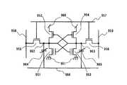
近年、これらの問題を克服するために、図19に示したような6個のトランジスタから構成される従来のSRAMに2つの強誘電体キャパシタを付加して不揮発性を実現する、図20に示す回路が提案されている(T.Miwa et al.、Proceedings of Symposium on VLSI Circuits(2001))。図20に示した回路は、従来のSRAMを構成するN型トランジスタである第1、第3、第5、第6のトランジスタ951、953、955、956、P型トランジスタである第2及び第4のトランジスタ952、954の6個のトランジスタと、第1及び第2の強誘電体キャパシタ964、965とを備えている。これらのキャパシタは、SRAMの記憶ノードである第1のノード962及び第2のノード963と強誘電体分極制御線966との間に各々挿入されている。図20に示した回路の電源を切断する前には、強誘電体分極制御線966に所定のパルス電圧を印加して、2つの強誘電体キャパシタ964、965の分極の向きを相互に逆にする。電源投入時は、μsオーダ又はサブμsオーダで緩やかに電源線960の電圧を上昇させる。この時、電源線960の電圧上昇に伴って、第1のノード962及び第2のノード963の電圧が徐々に上昇する。ここで、強誘電体キャパシタ964、965のどちらか一方は、強誘電体キャパシタ反転のために他方よりも多くの電荷が必要となることから、第1のノード962と第2のノード963の電圧上昇の速度が異なるようになる。一旦第1のノード962及び第2のノード963の電圧が異なるようになれば、電圧が速く上昇した方のノードは電源線960の電源電圧と同じ電圧まで上昇し、他方のノードは接地線961の接地電圧まで下降して、安定化する。即ち、電源切断前に強誘電体分極制御線966に所定のパルス電圧を印加することによって、その時点でSRAMに記憶されている内容を第1及び第2の強誘電体キャパシタ964、965の分極状態として保持する。これによって、電源投入後に電源切断前のメモリ内容をSRAMに再現することができる。その後は、図20に示した回路は、通常のSRAMと同様の動作を行い、第1及び第2の強誘電体キャパシタ964,965はメモリの読み出し、書き込み制御には直接的には関与しない。
しかしながら、上記した従来の技術においては、以下の問題があった。第1に、メモリセル待機時のリーク電流が増大するという問題があった。一般に強誘電体はリーク電流を流しやすい。電源投入中はSRAMの特性のために、第1及び第2のノード962、963はどちらか一方が電源電圧になり、他方が接地電圧となる。従って、強誘電体分極制御線966を介して直列に接続されている2つの強誘電体キャパシタ964、965の両端、即ち第1及び第2のノード962、963の間には電源電圧が常時印加されていることになる。これがメモリセル待機時にリーク電流が増大する原因となっていた。SRAMは待機時リーク電流が少ないことが大きな特長であるが、図20の回路ではその特徴が損なわれる恐れがある。
第2に、メモリセルの書き込み・読み出し時の消費電力が増大するという問題があった。前述の通り、2つの強誘電体キャパシタ964、965は強誘電体分極制御線966を介して第1及び第2のノード962、963の間に接続されている。従って、これらの強誘電体キャパシタ964、965は、第1のビット線955と、第1のビット線955の逆の電圧レベルとなる第2のビット線956とを用いてメモリセルへのデータ書き込み・読み出しを行う際に、寄生容量として作用するために、余分な電荷が必要となり、メモリセルの書き込み・読み出し時の消費電力が増大する。
発明の開示
本発明は、上記の問題を解決すべく、待機時リーク電流や書き込み・読み出し時の消費電力の増大を生じることなく、回路接続情報やLUTパラメータなどの設定状態を電源切断後も保持可能な不揮発性メモリ回路及びその駆動方法並びにそのメモリ回路を用いた半導体装置を提供することを目的とする。
上記目的を達成する本発明に係る不揮発性メモリ回路は、各々のゲートが相互に接続され、かつ各々のドレインが第1のノードを間に挟んで接続された第1のトランジスタと第2のトランジスタから構成される第1のインバータ、各々のゲートが相互に接続され、かつ各々のドレインが第2のノードを間に挟んで接続された第3のトランジスタおよび第4のトランジスタから構成される第2のインバータ、ゲートにワード線が接続され、第1のビット線と前記第1のノードとの間に接続される第5のトランジスタ、およびゲートに前記ワード線が接続され、第2のビット線と前記第2のノードとの間に接続される第6のトランジスタを備え、前記第1のノードは、前記第3のトランジスタのゲートおよび第4のトランジスタのゲートに接続されており、前記第2のノードは、前記第1のトランジスタのゲートおよび第2のトランジスタのゲートに接続されており、前記第1のトランジスタのソースおよび前記第3のトランジスタのソースは接地線に接続されており、前記第2のトランジスタのソースおよび前記第4のトランジスタのソースは電源線に接続されており、さらに抵抗値が電気的に変更可能である第1の抵抗素子および第2の抵抗素子を備え、前記第1の抵抗素子および前記第2の抵抗素子とは、以下の位置関係の中から選択される第1から第4の位置関係のいずれか1つを満たしている:前記第1の抵抗素子が前記第1のトランジスタのソースと前記接地線との間に接続され、前記第2の抵抗素子が前記第3のトランジスタのソースと前記接地線との間に接続されている第1の位置関係、前記第1の抵抗素子が前記第2のトランジスタのソースと前記電源線との間に接続され、前記第2の抵抗素子が前記第4のトランジスタのソースと前記電源線との間に接続されている第2の位置関係、前記第1の抵抗素子が前記第1のノードと前記第1のトランジスタのドレインとの間に接続され、前記第2の抵抗素子が前記第2のノードと前記第3のトランジスタのドレインとの間に接続されている第3の位置関係、および前記第1の抵抗素子が前記第1のノードと前記第2のトランジスタのドレインとの間に接続され、前記第2の抵抗素子が前記第2のノードと前記第4のトランジスタのドレインとの間に接続されている第4の位置関係。ここで、接続とは、直接的な接続のみに限定されず、間に介在物を有する間接的な接続をも意味する。
上記目的を達成する本発明に係る不揮発性メモリ回路の駆動方法は、上記の本発明に係る不揮発性メモリ回路の駆動方法であって、前記不揮発性メモリ回路への電源供給を停止する前に、前記第1及び第2の抵抗素子を低抵抗状態にする第1ステップと、該第1ステップの後に前記第1及び第2の抵抗素子の何れか一方を高抵抗状態にする第2ステップとを含むストアステップ、及び前記不揮発性メモリ回路への電源供給が開始された後に、前記ワード線、前記第1及び第2ビット線、並びに前記電源線に所定のタイミングで電圧を印加するリコールステップを含んでいる。
上記目的を達成する第1の本発明に係る不揮発性メモリ回路を用いた半導体装置は、上記の本発明に係る不揮発メモリ回路をルックアップテーブルのパラメータ用のメモリに用いている。
上記目的を達成する第2の本発明に係る不揮発性メモリ回路を用いた半導体装置は、上記の本発明に係る不揮発メモリ回路を回路接続情報制御用メモリに用いている。
上記目的を達成する第3の本発明に係る不揮発性メモリ回路を用いた半導体装置は、上記の本発明に係る不揮発メモリ回路を備え、暗号処理用に使用される。
発明を実施するための最良の形態
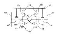
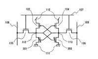
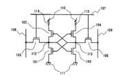
以下、本発明に係る半導体装置の実施の形態を添付図面を参照しながら説明する。図1は、本発明の実施形態に係る不揮発性メモリ回路を示す回路図である。本発明の実施の形態に係る不揮発性メモリ回路は、第1のインバータを構成する第1のトランジスタ101及び第2のトランジスタ102と、第2のインバータを構成する第3のトランジスタ103及び第4のトランジスタ104と、パストランジスタである第5のトランジスタ105及び第6のトランジスタ106と、ワード線107と、第1のビット線108及び第2のビット線109と、電源線110と、接地線111と、第1の抵抗素子114及び第2の抵抗素子115とを備えている。ここで、第1のインバータを構成する第1及び第2のトランジスタ101、102、並びに第2のインバータを構成する第3及び第4のトランジスタ103、104は、それぞれ相補型のトランジスタである。以下においては、第1、第3、第5及び第6のトランジスタ101、103、105、106がN型トランジスタであり、第2及び第4のトランジスタ102、104がP型トランジスタである場合について説明する。第3のトランジスタ103及び第4のトランジスタ104の相互に接続されたゲート(第2のインバータの入力端子)は、第1のトランジスタ101及び第2のトランジスタ102のドレインを相互に接続する第1のノード112(第1のインバータの出力端子)に接続され、第1のトランジスタ101及び第2のトランジスタ102の相互に接続されたゲート(第1のインバータの入力端子)は、第3のトランジスタ103及び第4のトランジスタ104のドレインを相互に接続する第2のノード113(第2のインバータの出力端子)に接続され、これらによってフリップフロップ回路が構成されている。図1に示した回路が従来のSRAM(図19)と異なる点は、第1及び第2の抵抗素子114、115が、第1のトランジスタ101のソースと接地線111との間、及び第3のトランジスタ103のソースと接地線111との間に、それぞれ配置されていることである。ここで、第1及び第2の抵抗素子114、115は、抵抗素子として形成された後にその抵抗値が変化され得る可変抵抗素子であり、例えば、GeSbTe等のカルコゲナイド化合物の相変化材料を用いた可変抵抗素子や、印加する磁界によって抵抗値を変化させ得るGMR(Giant Magnetic Resistance)素子、TMR(Tunneling Magnetic Resistance)素子等の可変抵抗素子である。
次に、図1に示した不揮発性メモリ回路の不揮発性、即ち電源切断後にもメモリ内容を保持する機能に関して説明する。詳細は後述することとして、ここでは概要のみを説明する。図1に示した不揮発性メモリ回路の不揮発性機能は、電源切断直前にメモリ内容を抵抗素子に保持させ(以下、STORE制御と記す)、元のメモリ内容を電源投入直後に再現する(以下、RECALL制御と記す)ことによって実現する。先ず、STORE制御では、第1及び第2の抵抗素子114、115として使用される可変抵抗素子に応じた所定の手段を用いて、第1及び第2の抵抗素子114、115の抵抗値を、いずれか一方の抵抗値が他方の抵抗値よりも大きくなるように変化させる。この変化後の抵抗値は、各々の抵抗変化素子によって保持される。例えば、第2の抵抗素子115の抵抗値が、第1の抵抗素子114の抵抗値の2倍になるように変化させたと仮定する。次に、RECALL制御では、ワード線107の電圧をローレベル(通常は0V)にして第1及び第2のビット線108、109からの影響をなくした上で、電源線110の電圧を0Vから徐々に大きくする。この時、第1及び第2の抵抗素子114、115が各々、第1のトランジスタ101のソース及び接地線111の間、第3のトランジスタ103のソース及び接地線111の間に接続されているために、第1及び第3のトランジスタ101、103に電流が流れ始めると、第1及び第2の抵抗素子114、115による電圧降下が生じ、第1及び第3のトランジスタ101、103のソース電圧が上昇する。これによって、第1及び第3のトランジスタ101、103の閾値(Vt)が見かけ上、上昇する。第2の抵抗素子115の抵抗値が、第1の抵抗素子114の抵抗値の2倍と仮定したので、第3のトランジスタ103のソース電位が第1のトランジスタ101のソース電位よりも上昇し、第3のトランジスタ103には第1のトランジスタ101に比べて電流が流れにくくなる。従って、第1のトランジスタ101に流れる電流によって第1のノード112の電圧は接地電圧に近くなる。第1のノード112は、第3のトランジスタ103のゲートと電気的に接続されているために、第3のトランジスタ103では、より一層電流が流れにくくなり、最終的に第1のノード112は接地電圧に達し、逆に第2のノード113は電源電圧に達して安定する。このように、第2の抵抗素子115の抵抗値が第1の抵抗素子114の抵抗値よりも大きければ、第1のノード112は接地電圧に達し、逆に第2のノード113は電源電圧に達することから、電源切断の直前に第1及び第2の抵抗素子114、115の抵抗値を、所定の大小関係になるように設定すれば、電源投入後にメモリセルのデータを再び所定の値にすることができる。即ち、図1に示した不揮発性メモリ回路は不揮発性機能を有する。
上記したSTORE制御は、第1及び第2の抵抗素子114、115に使用される可変抵抗素子の種類によって異なる。一例として、第1及び第2の抵抗素子114、115に、GeSbTe等の相変化材料を備えた抵抗変化素子を用いる場合について、図2、3を用いて説明する。図2は、図1に示した不揮発性メモリ回路の回路図において、STORE制御時における電圧、電流の一部を付記したものである。図3の(a)は、第1及び第3のトランジスタ101、103のドレイン電流−ドレイン電圧(Id−Vd)特性の一部を示した図であり、(b)は、STORE制御時のワード線107へのパルス電圧Vwordの印加タイミングと、第1及び第3のトランジスタ101、103のドレイン電流Ia、Ibの大きさとを示した図である。まず、第2のトランジスタ102と第4のトランジスタ104の影響をなくすために、電源線110への電源供給を遮断し、ワード線107の電圧をローレベル(通常は0V)にする。次に、第1のビット線108に電圧Vaを印加し、同時に第2のビット線109に電圧Vbを印加し、ワード線107をハイレベルにする。これによって、第1及び第3のトランジスタ101、103のゲート電圧VgがそれぞれVa、Vbとなる。ワード線107に印加する電圧は、電源電圧と同じ電圧であってもよく、ワード線107をゲート電極とする第5、第6のトランジスタ105、106での基板バイアス効果を避けるために、第1及び第2のビット線108、109の電圧Va、Vbの大きい方の電圧よりもさらに大きい電圧を印加してもよい。ワード線107をハイレベルにすると、第1のノード112には電圧Vaが印加され、第2のノード113には電圧Vbが印加される。よって、第1のトランジスタ101では、ゲート電圧Vg=Vb、ドレイン電圧Vd=Vaとなる。一方、第3のトランジスタ103では、ゲート電圧Vg=Va、ドレイン電圧Vd=Vbとなる。図3の(a)に示したId−Vd特性は、第1のトランジスタ101には電流Iaが流れ、第3のトランジスタ103には電流Ibが流れることを示している。ここで、第1及び第2の抵抗素子114、115はGeSbTe等の相変化材料で形成されているので、印加される電流値とその変化パターンによって抵抗値が変化する。即ち、相変化材料は、リセット電流Iy以上の電流を印加して、電流を急に切断して急冷するとアモルファス状態となり、高抵抗となる。一方、セット電流Ix以上かつリセット電流Iy未満の電流を印加して、電流を徐々に減少させて緩やかに冷却すると結晶化するため、低抵抗となる。そして、相変化材料はその状態を保持する。従って、第1のトランジスタ101にリセット電流Iyよりも大きい電流Iaが流れるように電圧Vaを設定し、第3のトランジスタ103にセット電流Ix以上且つリセット電流Iy未満の電流Ibが流れるように電圧Vbを設定し、ワード線107に電圧パルスVwordを印加すれば、第1の抵抗素子114を高抵抗にし、第2の抵抗素子115を低抵抗にすることができる。
次に、図1に示した不揮発性メモリ回路の駆動方法を詳細に説明する。本駆動方法は、上記したように、STORE制御及びRECALL制御を含んでいる。以下において、第1及び第2抵抗素子114、115は、GeSbTe等のカルコゲナイド化合物の相変化材料から構成されているとする。
(STORE制御)
先ず、STORE制御の詳細を説明する。STORE制御は、2つのステップを含んでいる。STORE制御の第1のステップでは、第1及び第2の抵抗素子114、115を共に結晶状態にして、低抵抗にする。第2のステップでは、第1又は第2の抵抗素子114、115の何れか一方のみをアモルファス状態にし、高抵抗にする。これら2つのステップによって、不揮発性メモリ回路に記憶されている情報、即ち記憶ノードである第1及び第2のノード112、113の電圧状態を、第1及び第2の抵抗素子114、115の抵抗値として保持する。
(第1のステップ)
図4は、STORE制御の第1のステップにおいて、図1に示した不揮発性メモリ回路の各線に電圧を印加するタイミングチャートである。WT、B1、B2、DDは、それぞれワード線107、第1のビット線108、第2のビット線109、電源線110の電圧を表す。第1のビット線108、第2のビット線109、電源線110に電源電圧Vddを印加した状態で、ワード線107に、第5及び第6のトランジスタ105、106がオンするハイレベルの電圧Vbtを印加(WT=Vbt)する。ここで、電圧Vbtは電源電圧Vddよりも大きくてもよい。この状態を時間Taの間維持した後、ワード線107の電圧WT=Vbtを第5及び第6のトランジスタ105、106がオフするローレベルの電圧、例えば0Vに急激に戻す。これによって、第5及び第6のトランジスタ105、106が導通状態になり、第1及び第2のノード112、113の電圧が電源電圧Vdd付近まで増大する。従って、第1及び第3のトランジスタ101、103が導通状態になり、第1及び第2の抵抗素子114、115に電流が流れる。
相変化材料は、上記したように、ある一定以上のジュール熱を与えた後、徐々に冷却すれば、結晶状態になり、低抵抗になる。例えば、絶縁膜としてSiO2を用いた直径φ190nmの相変化材料を、結晶状態とするのに要する単位体積当りのジュール熱は約1.6pJであることが知られている(S.Tyson et al.、Aerospace Conference Proceedings、2000 IEEE vol.5 pp385−390)。
図1に示した不揮発性メモリ回路に関して、一例として、ワード線107に印加される電圧WT=Vbtを3.9V、印加する時間Taを100ns、第1及び第2の抵抗素子114、115の直径をφ190nm、絶縁膜としてSiO2を用い、初期状態において第2の抵抗素子115の抵抗値が第1の抵抗素子114の10倍であるとし、図4に示したタイミングチャートに従って電圧を印加する条件でシミュレーションを行い、第1のステップを解析した。
図5は、第1及び第2の抵抗素子114、115の各々に流れる電流Ia、Ibのシミュレーション結果を示すグラフである。図5では、時間軸(横軸)は、ワード線107へのパルス電圧(WT=Vbt)印加の開始時刻を0としている。図5に示したように、第1の抵抗素子114にはIa=100(μA)、第2の抵抗素子115にはIb=17(μA)の電流が流れることが分かる。これによって第1及び第2の抵抗素子114、115に発生するジュール熱は、それぞれ11pJ、1.6pJとなり、何れも徐々に冷却すれば、結晶状態になるのに十分な熱量である(S.Tyson et al.による上記文献参照)。
以上のように、STORE制御の第1のステップでは、第1のビット線108、第2のビット線109、電源線110に電源電圧Vddを印加した状態で、ワード線107にハイレベルの電圧Vbtを印加することによって、不揮発性メモリ回路の第1及び第3のトランジスタ101、103を導通状態にし、第1及び第2の抵抗素子114、115に結晶状態(低抵抗)となるために必要なジュール熱を与えることができる。
(第2のステップ)
図6は、STORE制御の第2のステップにおいて、図1に示した不揮発性メモリ回路の各線に電圧を印加するタイミングチャートである。符号の意味は、図4と同じである。第1及び第2の抵抗素子114、115は、何れも第1のステップによって結晶状態(低抵抗)になっており、その抵抗値はほぼ等しい値となっていると仮定する。第1のビット線108及び電源線110に電源電圧Vddを、第2のビット線109に電源電圧Vddよりも小さい電圧Vbb2を印加した状態で、ワード線107にハイレベルの電圧Vbtを印加(WT=Vbt)する。ここで、電圧Vbtは電源電圧Vddよりも大きくてもよい。この状態を時間Tbの間維持し、その後、ワード線107の電圧WTをローレベル、例えば0Vに急激に戻す。これによって、時間Tbの間、第5及び第6のトランジスタ105、106が導通状態となり、第1のノード112の電圧が、第1のビット線108に印加された電源電圧Vdd付近の電圧Vaまで増大し、第2のノード113の電圧が、第2のビット線109に印加された電圧Vbb2付近の電圧Vbまで増大する。これにより、第1及び第3のトランジスタ101、103が導通状態になり、第1及び第2の抵抗素子114、115には、それぞれ電流Ia、Ibが流れる。また、時間Tbの後にWT=0になれば、Ia=Ib=0となる。第1及び第2の抵抗素子114、115を構成する相変化材料は上記したように、ある一定以上のジュール熱を与えて融点以上にし、急激に冷却すれば、アモルファス状態になり、高抵抗になる。絶縁膜にSiO2を用いた直径φ190nmの相変化材料を、アモルファス状態にするのに必要な単位体積当りのジュール熱は約3.6pJである(S.Tyson et al.による上記文献参照)。従って、電流Iaがアモルファス状態に要するリセット電流Iy以上になり、電流Ibが結晶状態に要するセット電流Ix以下になるように、第1及び第2ノード112、113に発生する電圧Va、Vbを設定し、即ち第1及び第2のビット線108、109に印加する電圧を適切な値に設定し、その後に電流Ia、Ibを急激に0にする。これによって、第1の抵抗素子114のみをアモルファス状態、即ち高抵抗とし、第2の抵抗素子115を結晶状態、即ち低抵抗のままに維持することができる。
図1に示した不揮発性メモリ回路に関して、一例として、第2のステップにおいて、ワード線107に印加される電圧WT=Vbtを3.9V、これを印加する時間Tbを30ns、第1のビット線108の電圧B1を電源電圧Vdd、第2のビット線109の電圧B2=Vbb2を1.5V、第1のステップ直後の第1及び第2の抵抗素子114、115の抵抗値を共に10kΩとし、図6に示したタイミングチャートで電圧を印加する条件でシミュレーションを行い、第2のステップを解析した。
図7は、第1及び第2の抵抗素子114、115に流れる電流Ia、Ibのシミュレーション結果を、図5と同様に示すグラフである。図7に示したように、安定状態において、第1の抵抗素子114にIa=109(μA)、第2の抵抗素子115にIb=31(μA)の電流が流れることが分かる。これによって第1及び第2の抵抗素子114、115に発生するジュール熱は、それぞれ3.7pJ、0.35pJとなる。従って、電流値が急激に0になり、急激に冷却された場合、第1の抵抗素子114がアモルファス状態(高抵抗)になるのに対して、第2の抵抗素子115は結晶状態(低抵抗)を維持する(S.Tyson et al.による上記文献参照)。
以上のように、STORE制御の第2のステップでは、第1のビット線108に電源電圧Vddを、第2のビット線109に1.5Vの電圧をそれぞれ印加した状態で、ワード線110にハイレベルの電圧を印加することによって、不揮発性メモリ回路のN型MOSトランジスタ101、103を導通状態にし、第1の抵抗素子114のみにアモルファス状態になるのに必要なジュール熱を発生させることが可能となる。
上記とは逆に、第1の抵抗素子114を低抵抗(結晶状態)に維持し、第2の抵抗素子115を高抵抗(アモルファス状態)にするためには、第1のビット線108、第2のビット線109に印加する電圧を上記と逆、即ちB1=Vbb2、B2=Vddと設定して、ワード線107にハイレベルのパルス電圧Vbtを印加すればよい。
このように、STORE制御の第1及び第2のステップによって、不揮発性メモリ回路に記憶されている情報を、第1及び第2の抵抗素子114、115の抵抗値として保持させることが可能となる。
(RECALL制御)
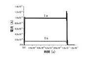
次に、RECALL制御について図8、9を用いて説明する。ここでは、上記したSTORE制御の結果、第1の抵抗素子114の抵抗値が、第2の抵抗素子115の抵抗値の10倍になっていると仮定する。図8は、RECALL制御時における、図1に示した不揮発性メモリ回路の各線に電圧を印加するタイミングチャートである。電源線110に印加する電圧DDを、0Vから緩やかに上昇させ、上昇開始から時間Tc後にVddになった後、この状態を保持する。第1及び第2のビット線108、109のそれぞれに印加する電圧B1、B2も、電圧DDと同じタイミングで、時間TCの間0VからVddまで上昇させる。また、その時間Tcの間、ワード線107にはハイレベルの電圧Vddを印加する。これによって、第5及び第6のMOSトランジスタ105、106が導通状態になり、第1及び第2のノード112、113の電圧が電源電圧付近まで上昇する。従って、第1及び第3のトランジスタ101、103が導通状態になり、第1及び第2の抵抗素子114、115に電流が流れる。ここで、第1の抵抗素子114の抵抗値が第2の抵抗素子115の抵抗値の10倍なので、第1及び第3のトランジスタ101、103のソース電圧に差が生じ、第1のトランジスタ101のソース電圧の方が第3のトランジスタ103のソース電圧よりも大きくなる。第1及び第3のトランジスタ101、103の基板は接地線111に接続されているので、第1及び第3のトランジスタ101、103に基板バイアス効果が生じる。ソース電圧が大きい方が基板バイアス効果によりトランジスタの実効閾値が大きくなるので、本条件の場合、第1のトランジスタ101の方が第3のトランジスタ103よりも閾値が大きくなる。従って、第1のトランジスタ101がオンしにくく、第3のトランジスタ103がオンし易くなり、第1のノード112はハイレベルに、第2のノード113はローレベルに保持される。
一例として、図1におけるMOSトランジスタ101〜106の最小ゲート長を0.35μm、電源電圧Vddを3.3V、電源復帰時に電源線110に印加する電圧DDの上昇時間Tcを100ns、第2の抵抗素子115の抵抗値をMOSトランジスタのオン抵抗の値と同程度の10kΩ、第1の抵抗素子114の抵抗値を第2の抵抗素子115の抵抗値の10倍の100kΩとし、図8に示したタイミングチャートで電圧を印加する条件でシミュレーションを行い、RECALL制御を解析した。
図9は、第1及び第2のノード112、113に発生する電圧Va、Vbのシミュレーション結果を示すグラフである。図9に示したように、第1及び第2のノード112、113の電圧Va、Vbは、制御を開始した直後からしばらくの間は、何れも同様に上昇するが、約2Vまで上昇した後は、第1及び第2のノード112、113の電圧Va、Vbに差が生じた。さらに、制御を開始してから約100ns後の定常状態では、第1のノード112の電圧Vaは電源電圧Vdd(3.3V)となり、第2のノード113の電圧Vbは0Vに下がった。このように、シミュレーションによって、第1及び第2の抵抗素子114、115の抵抗値に差があれば、第1及び第3のトランジスタ101、103の内、より小さい抵抗値の抵抗素子が接続されている方が先にオンし、それによって第1及び第2のノード112、113の電圧がそれぞれ決定されることが確認された。上記では、第1の抵抗素子114の抵抗値を第2の抵抗素子115の抵抗値の10倍としてシミュレーションした結果を示したが、2倍程度の条件でシミュレーションを行った場合にも、図9に示したグラフと同様の結果が得られた。このことは、図1に示した不揮発性メモリ回路において、第1及び第2の抵抗素子114、115の抵抗比が、少なくとも2倍〜10倍と、比較的広い範囲内に設定されていれば、上記したRECALL制御が可能であること、即ち、上記したRECALL制御に関して、第1及び第2の抵抗素子114、115の抵抗比のマージンは非常に大きいことを意味する。
以上のように、本実施の形態に係る不揮発性メモリ回路のRECALL制御は、第5及第6のトランジスタ105、106をオン状態にし、抵抗値の異なる第1及び第2の抵抗素子114、115に電流を流し、第1及び第3のトランジスタ101、103の閾値に差を生じさせることによって、第1及び第2の抵抗素子114、115の抵抗値の違いとして保持されていた情報を、第1及び第2のノード112、113の電圧として再現することができる。また、RECALL制御において、第1及び第2の抵抗素子114、115の抵抗比のマージンは非常に大きく、第1及び第2の抵抗素子114、115の抵抗値の大小関係が逆転しない限り、正常なRECALL制御が可能であり、抵抗値のバラツキや変動に対しても動作が安定である。
上記したRECALL制御においては、第1及び第2のビット線108、109、電源線110の電圧B1、B2、DDを徐々に上昇させる場合を説明したが、これに限定されるものではなく、不揮発性メモリ回路が動作を開始する電源電圧近傍において、第1及び第3のトランジスタ101、103の閾値が十分異なるようになればよい。従って、第1及び第2のビット線108、109の電圧B1、B2を所定の電圧に固定しておき、電源線110の電圧DDだけを徐々に上昇させてもよく、ワード線107の電圧WT及び電源線110の電圧DDを徐々に上昇させてもよい。また、RECALL制御における時間Tcは100nsに限定されず、約1ns程度の短時間でもよい。
図1に示した不揮発性メモリ回路は、電源電圧Vddが供給されている通常の動作時には、メモリの記憶情報を読み出すREAD動作及びメモリに情報を書き込むWRITE動作を行う。READ動作では、パストランジスタである第5及び第6のトランジスタ105、106をオン状態にして、記憶ノードである第1及び第2のノード112、113の電圧を第1及び第2のビット線108、109を介して検知する。また、WRITE動作では、第1及び第2のビット線108、109を介して記憶ノードである第1及び第2のノード112、113を所定電圧に設定する。このとき、第1及び第2の抵抗素子114、115は、それぞれ第1及び第3のトランジスタ101、103のソースに接続されているため、READ動作及びWRITE動作において寄生抵抗として働かない。従って、消費電力の増大はほとんどない。
また、記憶ノードである第1及び第2のノード112、113は、それぞれ0V又は電源電圧Vddに保持されており、2つのインバータ(第1のトランジスタ101及び第2のトランジスタ102、並びに第3のトランジスタ103及び第4のトランジスタ104)に貫通電流がほとんど流れない。従って、待機時リーク電流もほとんど流れない。
また、READ動作時に、1pFの負荷容量からのディスチャージにより、第1のトランジスタ101から第1の抵抗素子114に電流が流れるときのジュール熱を、上記したシミュレーションと同じ条件でシミュレーションすれば、第1の抵抗素子114の抵抗値が低抵抗(結晶状態)の場合、約2.3pJであり、高抵抗(アモルファス状態)の場合、約0.015pJとなった。この結果を、相変化を生じる上記したジュール熱(結晶状態にするには約1.6pJ、アモルファス状態にするには約3.6pJ)と比較すれば、第1及び第2の抵抗素子114、115の抵抗値が高抵抗又は低抵抗の何れであったとしても、READ動作によって、第1及び第2の抵抗素子114、115の状態は変化しないことが分かる。即ち、READ動作によって、第1及び第2の抵抗素子114、115の抵抗値が変化することはない。
以上のように、本発明の実施の形態に係る不揮発性メモリ回路によれば、相変化材料を用いた2つの抵抗素子が、STORE制御の第1のステップで結晶状態になり、第2のステップで一方の抵抗素子のみがアモルファス状態になることによって、記憶情報を2つの抵抗素子の抵抗値として保持することが可能となり、これによって不揮発性を実現することができる。また、本発明の実施の形態に係る不揮発性メモリ回路は、待機時にリーク電流がほとんど流れず、従来のSRAMと比較して、WRITE動作、READ動作における消費電力がほとんど増大しない。また、RECALL制御において、ビット線の電圧を記憶ノードに与えることで、非常に安定な動作を実現することができる。さらに、トランジスタの数が従来のSRAMと同じ6個であり、増加しないので、新たなトランジスタを追加することによる消費電力の増加が生じない。
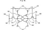
以上では、第1及び第2の抵抗素子114、115が、それぞれ、第1のトランジスタ101のソースと接地線111との間、第3のトランジスタ103のソースと接地線111との間に接続されている不揮発性メモリ回路に関して説明した(図1参照)が、これに限定されるものではない。例えば、図10に示すように、第1及び第2の抵抗素子114、115を、それぞれ、第2のトランジスタ102のソースと電源線110との間、第4のトランジスタ104のソースと電源線110との間に接続してもよい。この構成の場合、上記と同様に、第1及び第2の抵抗素子114、115は、第2及び第4のトランジスタ102、104に電流が流れ始めると、各々抵抗による電圧降下を生じ、ソース電圧を下降させる。これにより、P型トランジスタの閾値(Vt)が見かけ上、上昇し、第1の抵抗素子114と第2の抵抗素子115との抵抗値の違いにより、第1のノード112と第2のノード113の電圧上昇速度が異なることとなる。例えば、第2の抵抗素子115の抵抗値が、第1の抵抗素子114の抵抗値の2倍と仮定すると、第4のトランジスタ104のソース電圧が第2のトランジスタ102のソース電圧よりも低下し(P型のためN型と逆方向になる)、第4のトランジスタ104は第2のトランジスタ102に比べて電流が流れにくくなる。よって、第2のトランジスタ102に流れる電流によって第1のノード112の電圧は電源電圧に近い値になる。第1のノード112は、第4のトランジスタ104のゲート電極と電気的に接続されているため、第4のトランジスタ104はますます電流を流しにくくなり、最終的に第1のノード112は電源電圧に達し、逆に第2のノード113は接地電圧に達して安定化する。よって、図1に示した回路と同様に、第1及び第2の抵抗素子114、115の抵抗値を制御することによって、電源投入後の不揮発性メモリ回路のデータを決定することができる。即ち、図10に示した不揮発性メモリ回路に不揮発性機能を持たせることができる。図10に示した回路の場合、以上の通り、第1及び第2の抵抗素子114、115の抵抗値の違いにより、第1及び第2のノード112、113の電圧上昇速度が異なることを動作原理として用いている。よって、第1及び第2の抵抗素子114、115の抵抗値にばらつきがあっても、第1の抵抗素子114の抵抗値と第2の抵抗素子115の抵抗値との大小関係が逆転しない限り、上記した不揮発性は正常に機能する。よって、図10に示した不揮発性メモリ回路は、第1及び第2の抵抗素子114、115の抵抗値のばらつきや変動の影響を受けにくい回路構成となっている。
図10に示した不揮発性メモリ回路の駆動方法は、上記した図1に示した不揮発性メモリ回路の駆動方法と同様であるが、第1のビット線108、第2のビット線109に印加する電圧が異なる。即ち、STORE制御の第1ステップにおいて、第1及び第2のビット線108、109を共に0Vに維持した状態で、ワード線107にハイレベルのパルス電圧を印加し、第2ステップにおいて、第1及び第2のビット線108、109の何れか一方を0Vにし、他方を0Vよりも高い電圧にした状態で、ワード線107にハイレベルのパルス電圧を印加すればよい。RECALL制御のタイミングチャートは、図8と同様である。
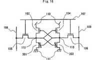
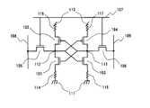
図1、図10に示した不揮発性メモリ回路では、第1及び第3のトランジスタ101、103のソース、又は第2及び第4のトランジスタ102、104のソースの内、何れか一方にのみに第1及び第2の抵抗素子114、115が接続されているが、図11に示すように第1及び第3のトランジスタ101、103のソース、並びに第2及び第4のトランジスタ102、104のソースに、第1〜第4の抵抗素子114〜117が接続されていてもよい。図11に示した不揮発性メモリ回路は、電源電圧が低く、且つ抵抗素子の抵抗値の可変範囲が小さいが、動作マージンを大きく確保したい場合、あるいはトランジスタ特性のばらつきが大きい場合などに有効である。この場合、第1及び第2の抵抗素子114、115の抵抗値の大小関係は、第3及び第4の抵抗素子116、117の抵抗値の大小関係と逆に設定することが必要である。例えば、第2の抵抗素子115の抵抗値を、第1の抵抗素子114の抵抗値よりも大きく設定する場合、第3の抵抗素子116の抵抗値を、第4の抵抗素子117の抵抗値よりも大きく設定する必要がある。
図11に示した不揮発性メモリ回路の駆動方法のRECALL制御は、上記した図1に示した不揮発性メモリ回路のRECALL制御と同じであるが、STORE制御では、図1及び図10の不揮発性メモリ回路のSTORE制御を組み合わせた制御を行えばよい。即ち、図1の不揮発性メモリ回路に関して説明したSTORE制御で、第1及び第2の抵抗素子114、115の抵抗値を設定し、図10の不揮発性メモリ回路に関して説明したSTORE制御で、第3及び第4の抵抗素子116、117の抵抗値を設定する。
また、図1、図10、図11に示した回路は、N型トランジスタとP型トランジスタの両方を用いたCMOS型の不揮発性メモリ回路であるが、これらに限定されるわけではない。例えば、P型トランジスタである第2のトランジスタ102及び第4のトランジスタ104の代わりに、デプレッション型のN型トランジスタ、又はノンドープポリシリコンなどで形成される高抵抗素子を使用してもよい。また、不揮発性メモリ回路を構成するN型トランジスタを全てP型トランジスタに置き換えてもよい。
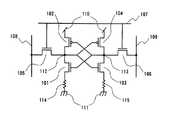
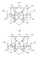
また、以上では、第1及び第3のトランジスタ101、103は、第1及び第2の抵抗素子114、115による電圧降下分だけ接地線111よりも高い電圧をソース電圧として動作する場合を説明したが、これに限定されるものではない。第1及び第2の抵抗素子114、115の何れか一方にリセット電流Iyよりも大きい電流が流れ、他方にはセット電流Ix以上且つリセット電流Iy未満の電流が流れる条件を満たすならば、どのような電圧の組み合わせでもよい。例えば、第1及び第2の抵抗素子114、115の特性と、第1及び第3のトランジスタ101、103の特性との組み合わせによっては、図1に示した不揮発性メモリ回路へのデータ書き込み、即ちSTORE制御を適切に行うことができない場合が考えられる。その場合には、図12の(a)に示すように、第1及び第2の抵抗素子114、115を、それぞれ、第1のトランジスタ101と第1のノード112との間、第3のトランジスタ103と第2のノード113との間に接続することが有効である。このように接続すれば、接地線111をソースとして動作させた場合に、ソース電圧が第1及び第2の抵抗素子114、115によって影響を受けることがないので、電流Ia及び電流Ibは第1及び第2の抵抗素子114、115によってあまり影響されなくなる。図12の(a)示した不揮発性メモリ回路の駆動方法は、図1に示した不揮発性メモリ回路の駆動方法と同様である。また、図12の(b)に示すように、第1及び第2の抵抗素子114、115を、それぞれ、第1のノード112と第2のトランジスタ102との間、第2のノード113及び第4のトランジスタ104との間に接続することも同様に有効である。図12(b)に示した不揮発性メモリ回路の駆動方法は、図10に示した不揮発性メモリ回路の駆動方法と同様である。
また、以上では、第1及び第2の抵抗素子114、115として、GeSbTe等の相変化材料を使用する場合について説明したが、これに限定されるものではない。As等を含む他のカルコゲナイド化合物等の相変化材料を用いてもよく、ペロブスカイト系の強相関電子材料を用いてもよい。また、磁界を印加して抵抗値を変化させることができる素子、例えばGMR素子、TMR素子等を使用してもよい。
図13の(a)は、TMR素子を用いた不揮発性メモリ回路を示す回路図である。図13の(b)は、第1及び第2の抵抗素子114、115、第1及び第2の磁界制御線154、155付近の3次元構造を模式的に示す斜視図である。図13の(b)は、(a)に示した回路図と上下が逆になっている。図13の(b)において、第1及び第2の抵抗素子114、115は、スピンの方向が変更可能な自由磁性体層、及びスピンが所定の方向に固定されている固定磁性体層の2つの磁性体層で、絶縁層を挟んだ3層構造を備えている(何れも図示せず)。ここで、TMR素子である第1及び第2の抵抗素子114、115の自由磁性体層は、印加される磁界の方向によってスピンの方向が変化され、2つの磁性体層(自由磁性体層及び固定磁性体層)のスピンが平行であるか、又は反平行であるかによって抵抗値が変化する。より具体的に説明すれば、例えば、接地線111と第1の磁界制御線154にそれぞれ所定方向の電流を流すと、これらの電流が発生する磁界の合成磁界によって、第1の抵抗素子114の自由磁性体層のスピンの方向を設定できる。このとき、設定された第1の抵抗素子114の自由磁性体層のスピンの方向が、固定磁性体層のスピンの方向と平行になったとすれば、第1の抵抗素子114の抵抗値は小さくなる。また、接地線111と第1の磁界制御線154に流す電流の方向を逆にすれば、第1の抵抗素子114の自由磁性体層のスピンの方向が固定磁性体層のスピンの方向と反平行になり、第1の抵抗素子114の抵抗値は大きくなる。同様に、接地線111及び第2の磁界制御線155を使用すれば、第2の抵抗素子115の抵抗値を設定することができる。従って、設置線111、第1及び第2の磁界制御線154、155の各々に流す電流方向を制御することによって、第1及び第2の抵抗素子114、115の抵抗値を所定の大小関係に設定することができる。
図13の(b)に示した不揮発性メモリ回路では、第1及び第2の磁界制御線154、155を備え、これらと交差する接地線111を磁界制御に使用しているが、図14に示したように、接地線111と平行に第3の磁界制御線156を備えてもよい。図14に示した不揮発性メモリ回路でメモリセルアレイを構成すれば、あるメモリセルへのデータの書き込みを第1〜第3の磁界制御線154〜156を用いた磁界制御によって行い、同時に別のメモリセルからデータの読み出しをワード線107、第1及び第2のビット線108、109によって行うことができる。
また、以上では、第1及び第2の抵抗素子114、115を備え、これらの抵抗値を制御することによって、電源投入後に不揮発性メモリ回路のデータを再現しているが、これに限定されるものではない。図1の第1のトランジスタ101及び第2のトランジスタ102で構成される第1のインバータと、第3のトランジスタ103及び第4のトランジスタ104で構成される第2のインバータとの特性差を作り出すことができれば、電源投入後にデータを再現することができる。例えば、図15に示すような構成のメモリ回路であってもよい。図15に示した回路は、図1の回路における第1のトランジスタ101及び第1の抵抗素子114、並びに第3のトランジスタ103及び第2の抵抗素子115を、各々浮遊ゲートを有する第1及び第3のトランジスタ201、203に変更した不揮発性メモリ回路である。この不揮発性メモリ回路は、従来のSRAMの回路構成と同様に、浮遊ゲートを有する第1及び第3のトランジスタ201、203と、第5及び第6のトランジスタ105、106と、第2及び第4のトランジスタ102、104とによって構成されており、浮遊ゲートを有する第1のトランジスタ201及び第2のトランジスタ102で構成されるインバータと、浮遊ゲートを有する第3のトランジスタ203及び第4のトランジスタ104で構成されるインバータとの2つのインバータに関して、各々の入力端子と他方の出力端子とが接続された構成となっている。浮遊ゲートを有する第1及び第3のトランジスタ201、203は、FN(Fowler Nordheim)電流やチャネル・ホット・エレクトロン(CHE:Channel Hot Electron)などにより各々の浮遊ゲートに電子を注入することによって、実効的な閾値が変化する。例えば、浮遊ゲートを有する第1のトランジスタ201の浮遊ゲートのみに電子を注入して実効的な閾値を高くした場合、浮遊ゲートを有する第1のトランジスタ201の電源投入時に流れるドレイン電流は、浮遊ゲートを有する第3のトランジスタ203に比べて小さくなるため、第1のノード112は、第2のノード113よりも電圧を高く保ち、電源電圧に達して安定化する。よって結果的に、浮遊ゲートを有する第1のトランジスタ201の閾値が、浮遊ゲートを有する第3のトランジスタ203の閾値よりも大きければ、第2のノード113は接地電圧に達し、一方第1のノード112は電源電圧に達するため、浮遊ゲートを有する第1及び第3のトランジスタ201、203の閾値を制御することによって、電源投入後に電源切断前のデータを再現することができる。このことは、図15に示したメモリ回路が不揮発性機能を有することを意味する。ここで、浮遊ゲートの形状は、従来の平板状であってもよく、ドット状であってもよい。また、浮遊ゲートは、上部の制御ゲートの下面全面に配置されていてもよく、ソース、ドレイン近傍の閾値制御に関して必要な部分のみに局所的に配置されていてもよい。
また、図16に示すように、図1の不揮発性メモリ回路における第1のトランジスタ101及び第1の抵抗素子114、並びに第3のトランジスタ103及び第2の抵抗素子115を、それぞれゲート上部に強誘電体キャパシタを有する第1及び第3のMFIS型トランジスタ301、303で置き換えて構成したメモリ回路であっても、上記と同様の効果を得ることができる。さらに、第1及び第3のMFIS型トランジスタ301、303は、MFMIS型トランジスタであってもよい。
本発明に係る不揮発性メモリ回路は、種々の応用が可能である。図17は、本発明に係る不揮発性メモリ回路を、ルックアップテーブルのメモリとして使用する場合の回路図である。図17に示したルックアップテーブルでは、4ビットの入力信号In0〜In3に対して、メモリセルSRAMに設定されている各々の値によって、出力信号Outが決定される。ここで、メモリセルSRAMに本発明に係る不揮発性メモリ回路を用いることによって、ルックアップテーブルに不揮発性機能を持たせることが可能となる。また、本発明に係る不揮発性メモリ回路は、図18の(a)に示したように、配線A、Bの間に設けられたパストランジスタのオン、オフによって、配線A、Bの接続、非接続の切替を行う回路において、パストランジスタのゲート電極を制御する回路接続情報制御用のメモリとしても用いることができる。さらに、本発明に係る不揮発性メモリ回路は、図18の(b)に示したように、双方向のデータフロー制御のためのトライステートバッファ制御用メモリとしても用いることができる。従って、本実施の形態に係る不揮発性メモリ回路を、ルックアップテーブルや回路接続情報制御用のメモリとして用いた半導体装置は、回路接続情報及びデータの何れをも電気的に変更可能であり、かつ外部観察では回路構成(配線間の接続の有無)やメモリ内容を判別されることがないため、高度の暗号処理用半導体装置として使用することができる。
なお、図1、図10、図11、図12の(a)および図12の(b)に示される不揮発性メモリ回路おいては、第1のトランジスタ101と接地線111との間、第3のトランジスタ103と接地線111との間には、トランジスタなどからなるスイッチング素子はいずれも存在していない。
産業上の利用の可能性
本発明によれば、メモリ内容を2つの抵抗変化素子の抵抗値の差異として保持し、電源投入後にメモリ内容を再現することができ、待機時リーク電流や書き込み・読み出し時の消費電力の増大を生じることがない不揮発性メモリ回路を実現することができ、回路接続情報やルックアップテーブルのパラメータの設定を電源切断後も保持可能な半導体装置を提供することができる。
【図面の簡単な説明】
第1図は、本発明の実施の形態に係る不揮発性メモリ回路を示す回路図である。
第2図は、図1に示した不揮発性メモリ回路の駆動方法を説明するための回路図である。
第3図は、図1に示した不揮発性メモリ回路に使用されるトランジスタの電流電圧特性を示す図である。
第4図は、図1に示した不揮発性メモリ回路のSTORE制御の第1のステップにおけるタイミングチャートである。
第5図は、図1に示した不揮発性メモリ回路のSTORE制御の第1のステップにおける抵抗素子に流れる電流のシミュレーション結果を示す図である。
第6図は、図1に示した不揮発性メモリ回路のSTORE制御の第2のステップにおけるタイミングチャートである。
第7図は、図1に示した不揮発性メモリ回路のSTORE制御の第2のステップにおける抵抗素子に流れる電流のシミュレーション結果を示す図である。
第8図は、図1に示した不揮発性メモリ回路のRECALL制御におけるタイミングチャートである。
第9図は、図1に示した不揮発性メモリ回路のRECALL制御における記憶ノードの電圧のシミュレーション結果を示す図である。
第10図は、図1に示した不揮発性メモリ回路において抵抗素子の位置を変更した回路図である。
第11図は、図1に示した不揮発性メモリ回路において抵抗素子をさらに付加した回路図である。
第12図の(a)、(b)は、図1に示した不揮発性メモリ回路において抵抗素子の位置をさらに変更した回路図である。
第13図の(a)は、図1に示した不揮発性メモリ回路において抵抗素子としてTMR素子を使用した回路図であり、(b)は抵抗素子部分の概略構造を示す斜視図である。
第14図は、図13の(a)に示した不揮発性メモリ回路において磁界制御線をさらに付加した抵抗素子部分の概略構造を示す斜視図である。
第15図は、図1に示した不揮発性メモリ回路において直列接続されたN型トランジスタ及び抵抗素子を、浮遊ゲートを有するN型トランジスタで置き換えた回路図である。
第16図は、図1に示した不揮発性メモリ回路において直列接続されたN型トランジスタ及び抵抗素子を、強誘電体キャパシタを有するN型トランジスタで置き換えた回路図である。
第17図は、本発明の実施の形態に係る不揮発性メモリ回路を応用したLUTの回路図である。
第18図の(a)は、本発明の実施の形態に係る不揮発性メモリ回路を配線間の接続制御に応用した回路図であり、(b)は本発明の実施の形態に係る不揮発性メモリ回路をトライステートバッファに応用した回路図である。
第19図は、従来のSRAMを示す回路図である。
第20図は、強誘電体を有する従来のSRAMを示す回路図である。TECHNICAL FIELD The present invention relates to a nonvolatile memory circuit, a driving method thereof, and a semiconductor device using the memory circuit. In particular, the circuit connection information can be rewritten after manufacture and the circuit connection information is retained even after the power is turned off. The present invention relates to a nonvolatile memory circuit which is an element of a reconfigurable LSI, a driving method thereof, and a semiconductor device using the memory circuit.
Background Art In recent years, with the acceleration of development of new products in the electronics field, the development cycle of LSIs, which occupy the central position of electronic products, has become shorter. In addition, new products that are developed one after another are required to expand the functions of LSIs and improve their performance, so that the product life of various LSIs is shortening. New functions that are required to be applied to products become sophisticated, and there is a case where a request to change specifications after completing LSI design and entering a manufacturing stage may occur. On the other hand, in such an environment, sufficient time cannot be taken for verification after LSI design, so there is a possibility that a bug (defect) exists in the hardware or software and the manufacturing stage may be entered. Changes are required.
In view of these requirements, reconfigurable LSIs such as field programmable gate arrays (FPGAs) that can change circuit connection information after manufacturing have attracted attention. In the FPGA, circuit connection information and setting information in a look-up table (LUT), that is, parameters are stored in the SRAM. The SRAM loses its memory contents when power is cut off and power is not supplied. For this reason, when configuring a system using an FPGA, a nonvolatile memory such as an EEPROM is provided separately from the FPGA, and circuit connection information and LUT parameters are read from the nonvolatile memory every time the power is turned on and power supply is started. I was downloading. In such a configuration, the system cannot be operated until the circuit connection information and LUT parameters are downloaded from the non-volatile memory after the power is turned on. Therefore, the system is required to operate immediately after the power is turned on. Is not suitable. In order to reduce power consumption, it is desirable to manage power supply for each block in the LSI, but circuit connection information and LUT parameters are downloaded every time power supply is started again after power is turned off as described above. If this is necessary, it is impossible to turn off the power for each block, and it is difficult to realize a reduction in power consumption.
Therefore, a built-in EEPROM has been developed as an FPGA that retains circuit connection information and LUT parameters even after the power is turned off. However, in order to incorporate the EEPROM in the FPGA chip, there is a problem that the manufacturing process becomes complicated and the cost becomes high. The EEPROM also has a problem that the rewriting operation is slow, that is, it takes a long time to rewrite data.
In recent years, in order to overcome these problems, non-volatility is realized by adding two ferroelectric capacitors to a conventional SRAM composed of six transistors as shown in FIG. A circuit has been proposed (T. Miwa et al., Proceedings of Symposium on VLSI Circuits (2001)). The circuit shown in FIG. 20 includes first, third, fifth, and
However, the conventional techniques described above have the following problems. First, there is a problem that the leakage current during standby of the memory cell increases. In general, a ferroelectric easily causes a leakage current to flow. During power-on, due to the characteristics of the SRAM, one of the first and
Second, there is a problem that power consumption during writing / reading of the memory cell increases. As described above, the two
DISCLOSURE OF THE INVENTION In order to solve the above problem, the present invention maintains circuit connection information, LUT parameters, and other setting states even after power-off without causing an increase in standby leakage current and power consumption during writing / reading. An object of the present invention is to provide a possible nonvolatile memory circuit, a driving method thereof, and a semiconductor device using the memory circuit.
The non-volatile memory circuit according to the present invention that achieves the above object includes a first transistor and a second transistor in which the gates are connected to each other and the drains are connected with the first node in between. A second inverter composed of a third transistor and a fourth transistor each having a gate connected to each other and each drain connected across the second node. An inverter having a gate connected to a word line, a fifth transistor connected between the first bit line and the first node, and a gate connected to the word line connected to the second bit line; A sixth transistor connected to the second node, wherein the first node is connected to a gate of the third transistor and a gate of the fourth transistor; The second node is connected to the gate of the first transistor and the gate of the second transistor, and the source of the first transistor and the source of the third transistor are connected to a ground line. And the source of the second transistor and the source of the fourth transistor are connected to a power supply line, and the resistance value can be electrically changed. The first resistance element and the second resistance element satisfy any one of first to fourth positional relationships selected from the following positional relationships: Are connected between the source of the first transistor and the ground line, and the second resistive element is connected between the source of the third transistor and the ground line. A first positional relationship, the first resistance element is connected between a source of the second transistor and the power line; and a second resistance element is connected to the source of the fourth transistor and the power line. A second positional relationship between the first node and the drain of the first transistor, and the second resistor element connected to the second node. A third positional relationship connected between the first node and the drain of the third transistor, and the first resistive element connected between the first node and the drain of the second transistor A fourth positional relationship in which the second resistance element is connected between the second node and the drain of the fourth transistor. Here, the connection is not limited to only a direct connection, but also means an indirect connection having an inclusion in between.
The non-volatile memory circuit driving method according to the present invention that achieves the above object is the above non-volatile memory circuit driving method according to the present invention, and before the power supply to the non-volatile memory circuit is stopped, A first step of bringing the first and second resistance elements into a low resistance state; and a second step of bringing one of the first and second resistance elements into a high resistance state after the first step. And a recall step of applying a voltage to the word line, the first and second bit lines, and the power supply line at a predetermined timing after power supply to the nonvolatile memory circuit is started. It is out.
The semiconductor device using the non-volatile memory circuit according to the first aspect of the present invention that achieves the above object uses the non-volatile memory circuit according to the present invention as a memory for a parameter of a lookup table.
The semiconductor device using the nonvolatile memory circuit according to the second aspect of the present invention that achieves the above object uses the nonvolatile memory circuit according to the present invention as a circuit connection information control memory.
A semiconductor device using the nonvolatile memory circuit according to the third aspect of the present invention that achieves the above object includes the above-described nonvolatile memory circuit according to the present invention and is used for cryptographic processing.
BEST MODE FOR CARRYING OUT THE INVENTION Embodiments of a semiconductor device according to the present invention will be described below with reference to the accompanying drawings. FIG. 1 is a circuit diagram showing a nonvolatile memory circuit according to an embodiment of the present invention. The nonvolatile memory circuit according to the embodiment of the present invention includes a
Next, the nonvolatile function of the nonvolatile memory circuit shown in FIG. 1, that is, the function of retaining the memory contents even after the power is turned off will be described. As the details will be described later, only the outline will be described here. The non-volatile function of the non-volatile memory circuit shown in FIG. 1 causes the memory contents to be held in a resistance element immediately before power-off (hereinafter referred to as STORE control), and the original memory contents are reproduced immediately after power-on (hereinafter referred to as power-on). This is realized by RECALL control). First, in the STORE control, the resistance values of the first and
The above-described STORE control differs depending on the type of variable resistance element used for the first and
Next, a method for driving the nonvolatile memory circuit shown in FIG. 1 will be described in detail. As described above, this driving method includes STORE control and RECALL control. In the following, it is assumed that the first and
(STORE control)
First, details of the STORE control will be described. The STORE control includes two steps. In the first step of the STORE control, both the first and
(First step)
FIG. 4 is a timing chart for applying a voltage to each line of the nonvolatile memory circuit shown in FIG. 1 in the first step of the STORE control. WT, B1, B2, and DD represent voltages of the
As described above, when the phase change material is gradually cooled after giving a certain amount of Joule heat or more, it becomes a crystalline state and has a low resistance. For example, it is known that the Joule heat per unit volume required to bring a phase change material having a diameter of 190 nm using SiO2 as an insulating film into a crystalline state is about 1.6 pJ (S. Tyson et al. Aerospace Conference Proceedings, 2000 IEEE vol. 5 pp 385-390).
With respect to the nonvolatile memory circuit shown in FIG. 1, as an example, the voltage WT = Vbt applied to the
FIG. 5 is a graph showing simulation results of the currents Ia and Ib flowing in the first and
As described above, in the first step of the STORE control, the high-level voltage Vbt is applied to the
(Second step)
FIG. 6 is a timing chart for applying a voltage to each line of the nonvolatile memory circuit shown in FIG. 1 in the second step of the STORE control. The meaning of the symbols is the same as in FIG. It is assumed that the first and
In the nonvolatile memory circuit shown in FIG. 1, as an example, in the second step, the voltage WT = Vbt applied to the
FIG. 7 is a graph showing the simulation results of the currents Ia and Ib flowing in the first and
As described above, in the second step of the STORE control, the power supply voltage Vdd is applied to the
On the contrary, in order to maintain the
As described above, the information stored in the nonvolatile memory circuit can be held as the resistance values of the first and
(RECALL control)
Next, RECALL control will be described with reference to FIGS. Here, it is assumed that the resistance value of the
As an example, the minimum gate length of the
FIG. 9 is a graph showing simulation results of the voltages Va and Vb generated at the first and
As described above, the RECALL control of the nonvolatile memory circuit according to the present embodiment turns on the fifth and
In the above-described RECALL control, the case where the voltages B1, B2, and DD of the first and
The nonvolatile memory circuit shown in FIG. 1 performs a READ operation for reading stored information in a memory and a WRITE operation for writing information to the memory during a normal operation in which the power supply voltage Vdd is supplied. In the READ operation, the fifth and
The first and
Further, when a Joule heat generated when a current flows from the
As described above, according to the nonvolatile memory circuit according to the embodiment of the present invention, the two resistance elements using the phase change material are in the crystalline state in the first step of the STORE control, and the second step. Thus, since only one of the resistance elements is in an amorphous state, stored information can be held as the resistance values of the two resistance elements, thereby realizing non-volatility. In the nonvolatile memory circuit according to the embodiment of the present invention, leakage current hardly flows during standby, and power consumption in the WRITE operation and the READ operation hardly increases as compared with the conventional SRAM. Further, in the RECALL control, a very stable operation can be realized by applying the voltage of the bit line to the storage node. Further, the number of transistors is the same as that of the conventional SRAM, which is not increased, and thus power consumption due to addition of a new transistor does not occur.
In the above, the first and
The driving method of the nonvolatile memory circuit shown in FIG. 10 is the same as the driving method of the nonvolatile memory circuit shown in FIG. 1 described above, but is applied to the
In the nonvolatile memory circuit shown in FIGS. 1 and 10, the first and
The RECALL control of the method for driving the nonvolatile memory circuit shown in FIG. 11 is the same as the RECALL control of the nonvolatile memory circuit shown in FIG. 1 described above. However, in the STORE control, the nonvolatile memory shown in FIGS. Control combined with STORE control of the circuit may be performed. That is, the resistance values of the first and
The circuits shown in FIGS. 1, 10, and 11 are CMOS nonvolatile memory circuits using both N-type transistors and P-type transistors, but are not limited thereto. For example, instead of the
In the above description, the case where the first and
In the above description, the case where the phase change material such as GeSbTe is used as the first and
FIG. 13A is a circuit diagram showing a nonvolatile memory circuit using a TMR element. FIG. 13B is a perspective view schematically showing a three-dimensional structure in the vicinity of the first and
In the nonvolatile memory circuit shown in FIG. 13B, the first and second magnetic
Further, in the above, the first and
Further, as shown in FIG. 16, the
The nonvolatile memory circuit according to the present invention can be applied in various ways. FIG. 17 is a circuit diagram when the nonvolatile memory circuit according to the present invention is used as a memory for a lookup table. In the look-up table shown in FIG. 17, the output signal Out is determined by each value set in the memory cell SRAM with respect to the 4-bit input signals In0 to In3. Here, by using the nonvolatile memory circuit according to the present invention for the memory cell SRAM, the lookup table can have a nonvolatile function. Further, as shown in FIG. 18A, the nonvolatile memory circuit according to the present invention connects and disconnects the wirings A and B by turning on and off the pass transistor provided between the wirings A and B. In a circuit for switching connections, it can also be used as a memory for controlling circuit connection information for controlling the gate electrode of a pass transistor. Further, as shown in FIG. 18B, the nonvolatile memory circuit according to the present invention can also be used as a tristate buffer control memory for bidirectional data flow control. Therefore, the semiconductor device using the nonvolatile memory circuit according to the present embodiment as a memory for controlling a lookup table or circuit connection information can electrically change both circuit connection information and data, and Since external observation does not discriminate the circuit configuration (whether or not wiring is connected) and the memory contents, it can be used as an advanced cryptographic processing semiconductor device.
Note that in the nonvolatile memory circuits shown in FIGS. 1, 10, 11, 12A and 12B, the
Industrial Applicability According to the present invention, memory contents can be held as a difference in resistance value between two resistance change elements, and the memory contents can be reproduced after power-on. A nonvolatile memory circuit that does not increase power consumption at the time can be realized, and a semiconductor device that can retain circuit connection information and lookup table parameter settings even after power-off can be provided.
[Brief description of the drawings]
FIG. 1 is a circuit diagram showing a nonvolatile memory circuit according to an embodiment of the present invention.
FIG. 2 is a circuit diagram for explaining a method of driving the nonvolatile memory circuit shown in FIG.
FIG. 3 is a diagram showing the current-voltage characteristics of the transistors used in the nonvolatile memory circuit shown in FIG.
FIG. 4 is a timing chart in the first step of STORE control of the nonvolatile memory circuit shown in FIG.
FIG. 5 is a diagram showing a simulation result of the current flowing through the resistance element in the first step of the STORE control of the nonvolatile memory circuit shown in FIG.
FIG. 6 is a timing chart in the second step of the STORE control of the nonvolatile memory circuit shown in FIG.
FIG. 7 is a diagram showing a simulation result of the current flowing through the resistance element in the second step of the STORE control of the nonvolatile memory circuit shown in FIG.
FIG. 8 is a timing chart in RECALL control of the nonvolatile memory circuit shown in FIG.
FIG. 9 is a diagram showing a simulation result of the voltage of the storage node in the RECALL control of the nonvolatile memory circuit shown in FIG.
FIG. 10 is a circuit diagram in which the position of the resistance element is changed in the nonvolatile memory circuit shown in FIG.
FIG. 11 is a circuit diagram in which a resistance element is further added to the nonvolatile memory circuit shown in FIG.
FIGS. 12A and 12B are circuit diagrams in which the position of the resistance element is further changed in the nonvolatile memory circuit shown in FIG.
FIG. 13A is a circuit diagram using a TMR element as a resistance element in the nonvolatile memory circuit shown in FIG. 1, and FIG. 13B is a perspective view showing a schematic structure of the resistance element portion.
FIG. 14 is a perspective view showing a schematic structure of a resistance element portion to which a magnetic field control line is further added in the nonvolatile memory circuit shown in FIG.
FIG. 15 is a circuit diagram in which the N-type transistor and the resistance element connected in series in the nonvolatile memory circuit shown in FIG. 1 are replaced with an N-type transistor having a floating gate.
FIG. 16 is a circuit diagram in which the N-type transistor and the resistance element connected in series in the nonvolatile memory circuit shown in FIG. 1 are replaced with an N-type transistor having a ferroelectric capacitor.
FIG. 17 is a circuit diagram of an LUT to which the nonvolatile memory circuit according to the embodiment of the present invention is applied.
FIG. 18A is a circuit diagram in which the nonvolatile memory circuit according to the embodiment of the present invention is applied to connection control between wirings, and FIG. 18B is a nonvolatile memory according to the embodiment of the present invention. It is the circuit diagram which applied the circuit to the tristate buffer.
FIG. 19 is a circuit diagram showing a conventional SRAM.
FIG. 20 is a circuit diagram showing a conventional SRAM having a ferroelectric.
【0005】
よび前記第1の抵抗素子が前記第1のノードと前記第2のトランジスタのドレインとの間に接続され、前記第2の抵抗素子が前記第2のノードと前記第4のトランジスタのドレインとの間に接続されている第4の位置関係。ここで、接続とは、直接的な接続のみに限定されず、間に介在物を有する間接的な接続をも意味する。
上記目的を達成する本発明に係る不揮発性メモリ回路の駆動方法は、上記の本発明に係る不揮発性メモリ回路の駆動方法であって、前記不揮発性メモリ回路への電源供給を停止する前に、前記第1及び第2の抵抗素子を低抵抗状態にする第1ステップと、該第1ステップの後に前記第1及び第2の抵抗素子の何れか一方を高抵抗状態にする第2ステップとを含むストアステップ、及び前記不揮発性メモリ回路への電源供給が開始された後に、前記ワード線、前記第1及び第2ビット線、並びに前記電源線に所定のタイミングで電圧を印加するリコールステップを含んでいる。
上記目的を達成する第1の本発明に係る不揮発性メモリ回路を用いた半導体装置は、上記の本発明に係る不揮発性メモリ回路をルックアップテーブルのパラメータ用のメモリに用いている。
上記目的を達成する第2の本発明に係る不揮発性メモリ回路を用いた半導体装置は、上記の本発明に係る不揮発性メモリ回路を回路接続情報制御用メモリに用いている。
上記目的を達成する第3の本発明に係る不揮発性メモリ回路を用いた半導体装置は、上記の本発明に係る不揮発性メモリ回路を備え、暗号処理用に使用される。
図面の簡単な説明
第1図は、本発明の実施の形態に係る不揮発性メモリ回路を示す回路図である。
第2図は、図1に示した不揮発性メモリ回路の駆動方法を説明するための回路図である。
第3図は、図1に示した不揮発性メモリ回路に使用されるトランジスタの電流電圧特性を示す図である。
第4図は、図1に示した不揮発性メモリ回路のSTORE制御の第1のステップにおけるタイミングチャートである。[0005]
And the first resistance element is connected between the first node and the drain of the second transistor, and the second resistance element is connected between the second node and the drain of the fourth transistor. 4th positional relationship connected between. Here, the connection is not limited to only a direct connection, but also means an indirect connection having an inclusion in between.
The non-volatile memory circuit driving method according to the present invention that achieves the above object is the above non-volatile memory circuit driving method according to the present invention, and before the power supply to the non-volatile memory circuit is stopped, A first step of bringing the first and second resistance elements into a low resistance state; and a second step of bringing one of the first and second resistance elements into a high resistance state after the first step. And a recall step of applying a voltage to the word line, the first and second bit lines, and the power supply line at a predetermined timing after power supply to the nonvolatile memory circuit is started. It is out.
The semiconductor device using the non-volatile memory circuit according to the first aspect of the present invention that achieves the above object uses the non-volatile memory circuit according to the present invention as a memory for a parameter of a lookup table.
The semiconductor device using the nonvolatile memory circuit according to the second aspect of the present invention that achieves the above object uses the nonvolatile memory circuit according to the present invention as a circuit connection information control memory.
A semiconductor device using the non-volatile memory circuit according to the third aspect of the present invention that achieves the above object includes the non-volatile memory circuit according to the present invention and is used for cryptographic processing.
BRIEF DESCRIPTION OF THE DRAWINGS FIG. 1 is a circuit diagram showing a nonvolatile memory circuit according to an embodiment of the present invention.
FIG. 2 is a circuit diagram for explaining a method of driving the nonvolatile memory circuit shown in FIG.
FIG. 3 is a diagram showing the current-voltage characteristics of the transistors used in the nonvolatile memory circuit shown in FIG.
FIG. 4 is a timing chart in the first step of STORE control of the nonvolatile memory circuit shown in FIG.
本発明は、不揮発性メモリ回路の駆動方法に係り、特に、製造後に回路接続情報の書き換えが可能であり、且つ電源切断後も回路接続情報を保持するリコンフィグラブル(Reconfigurable)LSIの要素素子である不揮発性メモリ回路の駆動方法に関する。The present invention relatesto a nonvolatile memorycircuits for drivinghow, in particular, can be rewritten in the circuit connection information after manufacture, the elements of reconfigurable (Reconfigurable) LSI for and hold the even circuit connection information after power off It relatesto non-volatile memorycircuitry of the drivehow an element.
近年、エレクトロニクス分野における新製品の開発が加速するのに伴い、エレクトロニクス製品の中心的な位置を占めるLSIの開発サイクルも短くなってきている。さらに、次々と開発される新製品において、LSIの機能拡張や、性能改善が要求されることから、各種LSIの製品寿命も短くなってきている。製品への適用が要望される新機能が高度になり、LSIの設計を完了し、製造段階に入った後にも仕様を変更したいとの要望が発生することがある。一方、このような環境では、LSI設計後の検証に十分な時間が取れないために、ハードウェアやソフトウェアにバグ(不具合)が存在したまま製造段階に移行する可能性もあり、この場合にも変更が必要となる。 In recent years, as the development of new products in the electronics field has accelerated, the development cycle of LSIs, which occupy the central position of electronic products, has also become shorter. In addition, new products that are developed one after another are required to expand the functions of LSIs and improve their performance, so that the product life of various LSIs is shortening. New functions that are required to be applied to products become sophisticated, and there is a case where a request to change specifications after completing LSI design and entering a manufacturing stage may occur. On the other hand, in such an environment, sufficient time cannot be taken for verification after LSI design, so there is a possibility that a bug (defect) exists in the hardware or software and the manufacturing stage may be entered. Changes are required.
これらの要求から、製造後に回路接続情報を変更することが可能なFPGA(Field Programmable Gate Array)などのリコンフィグラブルLSIが注目されている。FPGAでは、回路接続情報や、ルックアップテーブル(LUT)内の設定情報、即ちパラメータなどをSRAMに格納していた。SRAMは電源が切断されて電力が供給されなくなると、メモリ内容が消失してしまう。このため、FPGAを用いてシステムを構成する場合、FPGAとは別にEEPROM等の不揮発性メモリを備え、電源が投入されて電力が供給開始される毎に回路接続情報やLUTパラメータを不揮発性メモリからダウンロードしていた。このような構成では、システムは、電源が投入された後、不揮発性メモリから回路接続情報やLUTパラメータのダウンロードを完了するまでは稼動できないため、電源投入後直ちに稼動することが要求されるシステムには適さない。また、消費電力低減のために、LSI内のブロック毎に電源供給を管理することが望ましいが、前述の通り電源を切断した後に再度電源供給を開始する毎に回路接続情報やLUTパラメータをダウンロードすることが必要であれば、ブロック毎の電源切断を行うことができず、消費電力の低減を実現することが困難である。 In view of these requirements, reconfigurable LSIs such as field programmable gate arrays (FPGAs) that can change circuit connection information after manufacturing have attracted attention. In the FPGA, circuit connection information and setting information in a look-up table (LUT), that is, parameters are stored in the SRAM. The SRAM loses its memory contents when power is cut off and power is not supplied. For this reason, when configuring a system using an FPGA, a nonvolatile memory such as an EEPROM is provided separately from the FPGA, and circuit connection information and LUT parameters are read from the nonvolatile memory every time the power is turned on and power supply is started. I was downloading. In such a configuration, the system cannot operate until the circuit connection information and LUT parameters are downloaded from the non-volatile memory after the power is turned on. Therefore, the system is required to operate immediately after the power is turned on. Is not suitable. In order to reduce power consumption, it is desirable to manage power supply for each block in the LSI, but circuit connection information and LUT parameters are downloaded every time power supply is started again after power is turned off as described above. If this is necessary, it is impossible to turn off the power for each block, and it is difficult to realize a reduction in power consumption.
従って、回路接続情報やLUTパラメータが電源切断後も保持されるFPGAとして、EEPROM内蔵型のものが開発された。しかし、EEPROMをFPGAチップに内蔵するためには、製造プロセスが複雑となり、コスト高になってしまうという問題があった。また、EEPROMは書換動作が遅い、即ちデータの書き換えに長時間を要する問題もあった。 Therefore, a built-in EEPROM has been developed as an FPGA that retains circuit connection information and LUT parameters even after the power is turned off. However, in order to incorporate the EEPROM in the FPGA chip, there is a problem that the manufacturing process becomes complicated and the cost becomes high. The EEPROM also has a problem that the rewriting operation is slow, that is, it takes a long time to rewrite data.
近年、これらの問題を克服するために、図19に示したような6個のトランジスタから構成される従来のSRAMに2つの強誘電体キャパシタを付加して不揮発性を実現する、図20に示す回路が提案されている(T. Miwa et al.、Proceedings of Symposium on VLSI Circuits (2001))。図20に示した回路は、従来のSRAMを構成するN型トランジスタである第1、第3、第5、第6のトランジスタ951、953、955、956、P型トランジスタである第2及び第4のトランジスタ952、954の6個のトランジスタと、第1及び第2の強誘電体キャパシタ964、965とを備えている。これらのキャパシタは、SRAMの記憶ノードである第1のノード962及び第2のノード963と強誘電体分極制御線966との間に各々挿入されている。図20に示した回路の電源を切断する前には、強誘電体分極制御線966に所定のパルス電圧を印加して、2つの強誘電体キャパシタ964、965の分極の向きを相互に逆にする。電源投入時は、μsオーダ又はサブμsオーダで緩やかに電源線960の電圧を上昇させる。この時、電源線960の電圧上昇に伴って、第1のノード962及び第2のノード963の電圧が徐々に上昇する。ここで、強誘電体キャパシタ964、965のどちらか一方は、強誘電体キャパシタ反転のために他方よりも多くの電荷が必要となることから、第1のノード962と第2のノード963の電圧上昇の速度が異なるようになる。一旦第1のノード962及び第2のノード963の電圧が異なるようになれば、電圧が速く上昇した方のノードは電源線960の電源電圧と同じ電圧まで上昇し、他方のノードは接地線961の接地電圧まで下降して、安定化する。即ち、電源切断前に強誘電体分極制御線966に所定のパルス電圧を印加することによって、その時点でSRAMに記憶されている内容を第1及び第2の強誘電体キャパシタ964、965の分極状態として保持する。これによって、電源投入後に電源切断前のメモリ内容をSRAMに再現することができる。その後は、図20に示した回路は、通常のSRAMと同様の動作を行い、第1及び第2の強誘電体キャパシタ964,965はメモリの読み出し、書き込み制御には直接的には関与しない。
しかしながら、上記した従来の技術においては、以下の問題があった。第1に、メモリセル待機時のリーク電流が増大するという問題があった。一般に強誘電体はリーク電流を流しやすい。電源投入中はSRAMの特性のために、第1及び第2のノード962、963はどちらか一方が電源電圧になり、他方が接地電圧となる。従って、強誘電体分極制御線966を介して直列に接続されている2つの強誘電体キャパシタ964、965の両端、即ち第1及び第2のノード962、963の間には電源電圧が常時印加されていることになる。これがメモリセル待機時にリーク電流が増大する原因となっていた。SRAMは待機時リーク電流が少ないことが大きな特長であるが、図20の回路ではその特徴が損なわれる恐れがある。 However, the conventional techniques described above have the following problems. First, there is a problem that the leakage current during standby of the memory cell increases. In general, a ferroelectric easily causes a leakage current to flow. During power-on, due to the characteristics of the SRAM, one of the first and
第2に、メモリセルの書き込み・読み出し時の消費電力が増大するという問題があった。前述の通り、2つの強誘電体キャパシタ964、965は強誘電体分極制御線966を介して第1及び第2のノード962、963の間に接続されている。従って、これらの強誘電体キャパシタ964、965は、第1のビット線955と、第1のビット線955の逆の電圧レベルとなる第2のビット線956とを用いてメモリセルへのデータ書き込み・読み出しを行う際に、寄生容量として作用するために、余分な電荷が必要となり、メモリセルの書き込み・読み出し時の消費電力が増大する。 Second, there is a problem that power consumption during writing / reading of the memory cell increases. As described above, the two
本発明は、上記の問題を解決すべく、待機時リーク電流や書き込み・読み出し時の消費電力の増大を生じることなく、回路接続情報やLUTパラメータなどの設定状態を電源切断後も保持可能な不揮発性メモリ回路の駆動方法を提供することを目的とする。In order to solve the above-described problem, the present invention is a nonvolatile memory capable of holding circuit connection information, LUT parameters, and other setting states even after power is turned off without causing an increase in standby leakage current and power consumption during writing / reading. and to providea drivinghowsexual memorycircuits.
上記目的を達成する本発明に係る不揮発性メモリ回路の駆動方法は、各々のゲートが相互に接続され、かつ各々のドレインが第1のノードを間に挟んで接続された第1のトランジスタと第2のトランジスタから構成される第1のインバータ、各々のゲートが相互に接続され、かつ各々のドレインが第2のノードを間に挟んで接続された第3のトランジスタおよび第4のトランジスタから構成される第2のインバータ、ゲートにワード線が接続され、第1のビット線と前記第1のノードとの間に接続される第5のトランジスタ、およびゲートに前記ワード線が接続され、第2のビット線と前記第2のノードとの間に接続される第6のトランジスタを備え、前記第1のノードは、前記第3のトランジスタのゲートおよび第4のトランジスタのゲートに接続されており、前記第2のノードは、前記第1のトランジスタのゲートおよび第2のトランジスタのゲートに接続されており、前記第1のトランジスタのソースおよび前記第3のトランジスタのソースは接地線に接続されており、前記第2のトランジスタのソースおよび前記第4のトランジスタのソースは電源線に接続されており、さらに抵抗値が電気的に変更可能である第1の抵抗素子および第2の抵抗素子を備え、前記第1の抵抗素子および前記第2の抵抗素子とは、以下の位置関係の中から選択される第1から第4の位置関係のいずれか1つを満たしている不揮発性メモリ回路の駆動方法であって、前記不揮発性メモリ回路への電源供給を停止する前に、前記第1及び第2の抵抗素子を低抵抗状態にする第1ステップと、該第1ステップの後に前記第1及び第2の抵抗素子の何れか一方を高抵抗状態にする第2ステップとを含むストアステップ、及び前記不揮発性メモリ回路への電源供給が開始された後に、前記ワード線、前記第1及び第2ビット線、並びに前記電源線に所定のタイミングで電圧を印加するリコールステップを含んでいる:前記第1の抵抗素子が前記第1のトランジスタのソースと前記接地線との間に接続され、前記第2の抵抗素子が前記第3のトランジスタのソースと前記接地線との間に接続されている第1の位置関係、前記第1の抵抗素子が前記第2のトランジスタのソースと前記電源線との間に接続され、前記第2の抵抗素子が前記第4のトランジスタのソースと前記電源線との間に接続されている第2の位置関係、前記第1の抵抗素子が前記第1のノードと前記第1のトランジスタのドレインとの間に接続され、前記第2の抵抗素子が前記第2のノードと前記第3のトランジスタのドレインとの間に接続されている第3の位置関係、および前記第1の抵抗素子が前記第1のノードと前記第2のトランジスタのドレインとの間に接続され、前記第2の抵抗素子が前記第2のノードと前記第4のトランジスタのドレインとの間に接続されている第4の位置関係。Method for driving the nonvolatile memory circuit according to the present invention for achieving theabove Symbol object,a first transistor, each gate is connected are connected to each other, and the drain of each sandwiched between the first node A first inverter composed of a second transistor, composed of a third transistor and a fourth transistor each gate connected to each other and each drain connected across the second node A second inverter connected, a word line connected to the gate, a fifth transistor connected between the first bit line and the first node, and a gate connected to the word line, A sixth transistor connected between the bit line of the third transistor and the second node, wherein the first node includes a gate of the third transistor and a gate of the fourth transistor. And the second node is connected to the gate of the first transistor and the gate of the second transistor, and the source of the first transistor and the source of the third transistor are grounded. A first resistance element and a second resistance element whose resistance value can be electrically changed; and a source of the second transistor and a source of the fourth transistor are connected to a power supply line. The first resistance element and the second resistance element are non-volatilesatisfying any one of the first to fourth positional relationships selected from the following positional relationships: A first step of setting the first and second resistance elements in a low resistance state before stopping power supply to the nonvolatile memory circuit; A storage step including a second step of bringing one of the first and second resistance elements into a high resistance state after the step, and after the power supply to the nonvolatile memory circuit is started, the word line , Including a recall step of applying a voltage to the first and second bit lines and the power line at a predetermined timing: the first resistance element is connected between the source of the first transistor and the ground line; A first positional relationship in which the second resistance element is connected between the source of the third transistor and the ground line, and the first resistance element is connected to the ground of the second transistor. A second positional relationship in which the second resistance element is connected between the source of the fourth transistor and the power supply line, the first resistance element being connected between the source and the power supply line; Said A third position connected between the first node and the drain of the first transistor, and the second resistive element connected between the second node and the drain of the third transistor; And the first resistance element is connected between the first node and a drain of the second transistor, and the second resistance element is a drain of the second node and the fourth transistor. 4th positional relationship connected between.
以下、本発明に係る半導体装置の実施の形態を添付図面を参照しながら説明する。図1は、本発明の実施形態に係る不揮発性メモリ回路を示す回路図である。本発明の実施の形態に係る不揮発性メモリ回路は、第1のインバータを構成する第1のトランジスタ101及び第2のトランジスタ102と、第2のインバータを構成する第3のトランジスタ103及び第4のトランジスタ104と、パストランジスタである第5のトランジスタ105及び第6のトランジスタ106と、ワード線107と、第1のビット線108及び第2のビット線109と、電源線110と、接地線111と、第1の抵抗素子114及び第2の抵抗素子115とを備えている。ここで、第1のインバータを構成する第1及び第2のトランジスタ101、102、並びに第2のインバータを構成する第3及び第4のトランジスタ103、104は、それぞれ相補型のトランジスタである。以下においては、第1、第3、第5及び第6のトランジスタ101、103、105、106がN型トランジスタであり、第2及び第4のトランジスタ102、104がP型トランジスタである場合について説明する。第3のトランジスタ103及び第4のトランジスタ104の相互に接続されたゲート(第2のインバータの入力端子)は、第1のトランジスタ101及び第2のトランジスタ102のドレインを相互に接続する第1のノード112(第1のインバータの出力端子)に接続され、第1のトランジスタ101及び第2のトランジスタ102の相互に接続されたゲート(第1のインバータの入力端子)は、第3のトランジスタ103及び第4のトランジスタ104のドレインを相互に接続する第2のノード113(第2のインバータの出力端子)に接続され、これらによってフリップフロップ回路が構成されている。図1に示した回路が従来のSRAM(図19)と異なる点は、第1及び第2の抵抗素子114、115が、第1のトランジスタ101のソースと接地線111との間、及び第3のトランジスタ103のソースと接地線111との間に、それぞれ配置されていることである。ここで、第1及び第2の抵抗素子114、115は、抵抗素子として形成された後にその抵抗値が変化され得る可変抵抗素子であり、例えば、GeSbTe等のカルコゲナイド化合物の相変化材料を用いた可変抵抗素子や、印加する磁界によって抵抗値を変化させ得るGMR(Giant Magnetic Resistance)素子、TMR(Tunneling Magnetic Resistance)素子等の可変抵抗素子である。 Embodiments of a semiconductor device according to the present invention will be described below with reference to the accompanying drawings. FIG. 1 is a circuit diagram showing a nonvolatile memory circuit according to an embodiment of the present invention. The nonvolatile memory circuit according to the embodiment of the present invention includes a
次に、図1に示した不揮発性メモリ回路の不揮発性、即ち電源切断後にもメモリ内容を保持する機能に関して説明する。詳細は後述することとして、ここでは概要のみを説明する。図1に示した不揮発性メモリ回路の不揮発性機能は、電源切断直前にメモリ内容を抵抗素子に保持させ(以下、STORE制御と記す)、元のメモリ内容を電源投入直後に再現する(以下、RECALL制御と記す)ことによって実現する。先ず、STORE制御では、第1及び第2の抵抗素子114、115として使用される可変抵抗素子に応じた所定の手段を用いて、第1及び第2の抵抗素子114、115の抵抗値を、いずれか一方の抵抗値が他方の抵抗値よりも大きくなるように変化させる。この変化後の抵抗値は、各々の抵抗変化素子によって保持される。例えば、第2の抵抗素子115の抵抗値が、第1の抵抗素子114の抵抗値の2倍になるように変化させたと仮定する。次に、RECALL制御では、ワード線107の電圧をローレベル(通常は0V)にして第1及び第2のビット線108、109からの影響をなくした上で、電源線110の電圧を0Vから徐々に大きくする。この時、第1及び第2の抵抗素子114、115が各々、第1のトランジスタ101のソース及び接地線111の間、第3のトランジスタ103のソース及び接地線111の間に接続されているために、第1及び第3のトランジスタ101、103に電流が流れ始めると、第1及び第2の抵抗素子114、115による電圧降下が生じ、第1及び第3のトランジスタ101、103のソース電圧が上昇する。これによって、第1及び第3のトランジスタ101、103の閾値(Vt)が見かけ上、上昇する。第2の抵抗素子115の抵抗値が、第1の抵抗素子114の抵抗値の2倍と仮定したので、第3のトランジスタ103のソース電位が第1のトランジスタ101のソース電位よりも上昇し、第3のトランジスタ103には第1のトランジスタ101に比べて電流が流れにくくなる。従って、第1のトランジスタ101に流れる電流によって第1のノード112の電圧は接地電圧に近くなる。第1のノード112は、第3のトランジスタ103のゲートと電気的に接続されているために、第3のトランジスタ103では、より一層電流が流れにくくなり、最終的に第1のノード112は接地電圧に達し、逆に第2のノード113は電源電圧に達して安定する。このように、第2の抵抗素子115の抵抗値が第1の抵抗素子114の抵抗値よりも大きければ、第1のノード112は接地電圧に達し、逆に第2のノード113は電源電圧に達することから、電源切断の直前に第1及び第2の抵抗素子114、115の抵抗値を、所定の大小関係になるように設定すれば、電源投入後にメモリセルのデータを再び所定の値にすることができる。即ち、図1に示した不揮発性メモリ回路は不揮発性機能を有する。 Next, the nonvolatile function of the nonvolatile memory circuit shown in FIG. 1, that is, the function of retaining the memory contents even after the power is turned off will be described. As the details will be described later, only the outline will be described here. The non-volatile function of the non-volatile memory circuit shown in FIG. 1 causes the memory contents to be held in a resistance element immediately before power-off (hereinafter referred to as STORE control), and the original memory contents are reproduced immediately after power-on (hereinafter referred to as power-on). This is realized by RECALL control). First, in the STORE control, the resistance values of the first and
上記したSTORE制御は、第1及び第2の抵抗素子114、115に使用される可変抵抗素子の種類によって異なる。一例として、第1及び第2の抵抗素子114、115に、GeSbTe等の相変化材料を備えた抵抗変化素子を用いる場合について、図2、3を用いて説明する。図2は、図1に示した不揮発性メモリ回路の回路図において、STORE制御時における電圧、電流の一部を付記したものである。図3の(a)は、第1及び第3のトランジスタ101、103のドレイン電流−ドレイン電圧(Id−Vd)特性の一部を示した図であり、(b)は、STORE制御時のワード線107へのパルス電圧Vwordの印加タイミングと、第1及び第3のトランジスタ101、103のドレイン電流Ia、Ibの大きさとを示した図である。まず、第2のトランジスタ102と第4のトランジスタ104の影響をなくすために、電源線110への電源供給を遮断し、ワード線107の電圧をローレベル(通常は0V)にする。次に、第1のビット線108に電圧Vaを印加し、同時に第2のビット線109に電圧Vbを印加し、ワード線107をハイレベルにする。これによって、第1及び第3のトランジスタ101、103のゲート電圧VgがそれぞれVa、Vbとなる。ワード線107に印加する電圧は、電源電圧と同じ電圧であってもよく、ワード線107をゲート電極とする第5、第6のトランジスタ105、106での基板バイアス効果を避けるために、第1及び第2のビット線108、109の電圧Va、Vbの大きい方の電圧よりもさらに大きい電圧を印加してもよい。ワード線107をハイレベルにすると、第1のノード112には電圧Vaが印加され、第2のノード113には電圧Vbが印加される。よって、第1のトランジスタ101では、ゲート電圧Vg=Vb、ドレイン電圧Vd=Vaとなる。一方、第3のトランジスタ103では、ゲート電圧Vg=Va、ドレイン電圧Vd=Vbとなる。図3の(a)に示したId−Vd特性は、第1のトランジスタ101には電流Iaが流れ、第3のトランジスタ103には電流Ibが流れることを示している。ここで、第1及び第2の抵抗素子114、115はGeSbTe等の相変化材料で形成されているので、印加される電流値とその変化パターンによって抵抗値が変化する。即ち、相変化材料は、リセット電流Iy以上の電流を印加して、電流を急に切断して急冷するとアモルファス状態となり、高抵抗となる。一方、セット電流Ix以上かつリセット電流Iy未満の電流を印加して、電流を徐々に減少させて緩やかに冷却すると結晶化するため、低抵抗となる。そして、相変化材料はその状態を保持する。従って、第1のトランジスタ101にリセット電流Iyよりも大きい電流Iaが流れるように電圧Vaを設定し、第3のトランジスタ103にセット電流Ix以上且つリセット電流Iy未満の電流Ibが流れるように電圧Vbを設定し、ワード線107に電圧パルスVwordを印加すれば、第1の抵抗素子114を高抵抗にし、第2の抵抗素子115を低抵抗にすることができる。 The above-described STORE control differs depending on the type of variable resistance element used for the first and
次に、図1に示した不揮発性メモリ回路の駆動方法を詳細に説明する。本駆動方法は、上記したように、STORE制御及びRECALL制御を含んでいる。以下において、第1及び第2抵抗素子114、115は、GeSbTe等のカルコゲナイド化合物の相変化材料から構成されているとする。 Next, a method for driving the nonvolatile memory circuit shown in FIG. 1 will be described in detail. As described above, this driving method includes STORE control and RECALL control. In the following, it is assumed that the first and
(STORE制御)
先ず、STORE制御の詳細を説明する。STORE制御は、2つのステップを含んでいる。STORE制御の第1のステップでは、第1及び第2の抵抗素子114、115を共に結晶状態にして、低抵抗にする。第2のステップでは、第1又は第2の抵抗素子114、115の何れか一方のみをアモルファス状態にし、高抵抗にする。これら2つのステップによって、不揮発性メモリ回路に記憶されている情報、即ち記憶ノードである第1及び第2のノード112、113の電圧状態を、第1及び第2の抵抗素子114、115の抵抗値として保持する。(STORE control)
First, details of the STORE control will be described. The STORE control includes two steps. In the first step of the STORE control, both the first and
(第1のステップ)
図4は、STORE制御の第1のステップにおいて、図1に示した不揮発性メモリ回路の各線に電圧を印加するタイミングチャートである。WT、B1、B2、DDは、それぞれワード線107、第1のビット線108、第2のビット線109、電源線110の電圧を表す。第1のビット線108、第2のビット線109、電源線110に電源電圧Vddを印加した状態で、ワード線107に、第5及び第6のトランジスタ105、106がオンするハイレベルの電圧Vbtを印加(WT=Vbt)する。ここで、電圧Vbtは電源電圧Vddよりも大きくてもよい。この状態を時間Taの間維持した後、ワード線107の電圧WT=Vbtを第5及び第6のトランジスタ105、106がオフするローレベルの電圧、例えば0Vに急激に戻す。これによって、第5及び第6のトランジスタ105、106が導通状態になり、第1及び第2のノード112、113の電圧が電源電圧Vdd付近まで増大する。従って、第1及び第3のトランジスタ101、103が導通状態になり、第1及び第2の抵抗素子114、115に電流が流れる。(First step)
FIG. 4 is a timing chart for applying a voltage to each line of the nonvolatile memory circuit shown in FIG. 1 in the first step of the STORE control. WT, B1, B2, and DD represent voltages of the
相変化材料は、上記したように、ある一定以上のジュール熱を与えた後、徐々に冷却すれば、結晶状態になり、低抵抗になる。例えば、絶縁膜としてSiO2を用いた直径φ190nmの相変化材料を、結晶状態とするのに要する単位体積当りのジュール熱は約1.6pJであることが知られている(S. Tyson et al.、 Aerospace Conference Proceedings、 2000 IEEE vol.5 pp385-390)。As described above, when the phase change material is gradually cooled after giving a certain amount of Joule heat or more, it becomes a crystalline state and has a low resistance. For example, it is known that the Joule heat per unit volume required to bring a phase change material having a diameter of 190 nm using SiO2 as an insulating film into a crystalline state is about 1.6 pJ (S. Tyson et al. Aerospace Conference Proceedings, 2000 IEEE vol.5 pp385-390).
図1に示した不揮発性メモリ回路に関して、一例として、ワード線107に印加される電圧WT=Vbtを3.9V、印加する時間Taを100ns、第1及び第2の抵抗素子114、115の直径をφ190nm、絶縁膜としてSiO2を用い、初期状態において第2の抵抗素子115の抵抗値が第1の抵抗素子114の10倍であるとし、図4に示したタイミングチャートに従って電圧を印加する条件でシミュレーションを行い、第1のステップを解析した。With respect to the nonvolatile memory circuit shown in FIG. 1, as an example, the voltage WT = Vbt applied to the
図5は、第1及び第2の抵抗素子114、115の各々に流れる電流Ia、Ibのシミュレーション結果を示すグラフである。図5では、時間軸(横軸)は、ワード線107へのパルス電圧(WT=Vbt)印加の開始時刻を0としている。図5に示したように、第1の抵抗素子114にはIa=100(μA)、第2の抵抗素子115にはIb=17(μA)の電流が流れることが分かる。これによって第1及び第2の抵抗素子114、115に発生するジュール熱は、それぞれ11pJ、1.6pJとなり、何れも徐々に冷却すれば、結晶状態になるのに十分な熱量である(S. Tyson et al.による上記文献参照)。 FIG. 5 is a graph showing simulation results of the currents Ia and Ib flowing in the first and
以上のように、STORE制御の第1のステップでは、第1のビット線108、第2のビット線109、電源線110に電源電圧Vddを印加した状態で、ワード線107にハイレベルの電圧Vbtを印加することによって、不揮発性メモリ回路の第1及び第3のトランジスタ101、103を導通状態にし、第1及び第2の抵抗素子114、115に結晶状態(低抵抗)となるために必要なジュール熱を与えることができる。 As described above, in the first step of the STORE control, the high-level voltage Vbt is applied to the
(第2のステップ)
図6は、STORE制御の第2のステップにおいて、図1に示した不揮発性メモリ回路の各線に電圧を印加するタイミングチャートである。符号の意味は、図4と同じである。第1及び第2の抵抗素子114、115は、何れも第1のステップによって結晶状態(低抵抗)になっており、その抵抗値はほぼ等しい値となっていると仮定する。第1のビット線108及び電源線110に電源電圧Vddを、第2のビット線109に電源電圧Vddよりも小さい電圧Vbb2を印加した状態で、ワード線107にハイレベルの電圧Vbtを印加(WT=Vbt)する。ここで、電圧Vbtは電源電圧Vddよりも大きくてもよい。この状態を時間Tbの間維持し、その後、ワード線107の電圧WTをローレベル、例えば0Vに急激に戻す。これによって、時間Tbの間、第5及び第6のトランジスタ105、106が導通状態となり、第1のノード112の電圧が、第1のビット線108に印加された電源電圧Vdd付近の電圧Vaまで増大し、第2のノード113の電圧が、第2のビット線109に印加された電圧Vbb2付近の電圧Vbまで増大する。これにより、第1及び第3のトランジスタ101、103が導通状態になり、第1及び第2の抵抗素子114、115には、それぞれ電流Ia、Ibが流れる。また、時間Tbの後にWT=0になれば、Ia=Ib=0となる。第1及び第2の抵抗素子114、115を構成する相変化材料は上記したように、ある一定以上のジュール熱を与えて融点以上にし、急激に冷却すれば、アモルファス状態になり、高抵抗になる。絶縁膜にSiO2を用いた直径φ190nmの相変化材料を、アモルファス状態にするのに必要な単位体積当りのジュール熱は約3.6pJである(S. Tyson et al.による上記文献参照)。従って、電流Iaがアモルファス状態に要するリセット電流Iy以上になり、電流Ibが結晶状態に要するセット電流Ix以下になるように、第1及び第2ノード112、113に発生する電圧Va、Vbを設定し、即ち第1及び第2のビット線108、109に印加する電圧を適切な値に設定し、その後に電流Ia、Ibを急激に0にする。これによって、第1の抵抗素子114のみをアモルファス状態、即ち高抵抗とし、第2の抵抗素子115を結晶状態、即ち低抵抗のままに維持することができる。(Second step)
FIG. 6 is a timing chart for applying a voltage to each line of the nonvolatile memory circuit shown in FIG. 1 in the second step of the STORE control. The meaning of the symbols is the same as in FIG. It is assumed that the first and
図1に示した不揮発性メモリ回路に関して、一例として、第2のステップにおいて、ワード線107に印加される電圧WT=Vbtを3.9V、これを印加する時間Tbを30ns、第1のビット線108の電圧B1を電源電圧Vdd、第2のビット線109の電圧B2=Vbb2を1.5V、第1のステップ直後の第1及び第2の抵抗素子114、115の抵抗値を共に10kΩとし、図6に示したタイミングチャートで電圧を印加する条件でシミュレーションを行い、第2のステップを解析した。 In the nonvolatile memory circuit shown in FIG. 1, as an example, in the second step, the voltage WT = Vbt applied to the
図7は、第1及び第2の抵抗素子114、115に流れる電流Ia、Ibのシミュレーション結果を、図5と同様に示すグラフである。図7に示したように、安定状態において、第1の抵抗素子114にIa=109(μA)、第2の抵抗素子115にIb=31(μA)の電流が流れることが分かる。これによって第1及び第2の抵抗素子114、115に発生するジュール熱は、それぞれ3.7pJ、0.35pJとなる。従って、電流値が急激に0になり、急激に冷却された場合、第1の抵抗素子114がアモルファス状態(高抵抗)になるのに対して、第2の抵抗素子115は結晶状態(低抵抗)を維持する(S. Tyson et al.による上記文献参照)。 FIG. 7 is a graph showing the simulation results of the currents Ia and Ib flowing in the first and
以上のように、STORE制御の第2のステップでは、第1のビット線108に電源電圧Vddを、第2のビット線109に1.5Vの電圧をそれぞれ印加した状態で、ワード線110にハイレベルの電圧を印加することによって、不揮発性メモリ回路のN型MOSトランジスタ101、103を導通状態にし、第1の抵抗素子114のみにアモルファス状態になるのに必要なジュール熱を発生させることが可能となる。 As described above, in the second step of the STORE control, the power supply voltage Vdd is applied to the
上記とは逆に、第1の抵抗素子114を低抵抗(結晶状態)に維持し、第2の抵抗素子115を高抵抗(アモルファス状態)にするためには、第1のビット線108、第2のビット線109に印加する電圧を上記と逆、即ちB1=Vbb2、B2=Vddと設定して、ワード線107にハイレベルのパルス電圧Vbtを印加すればよい。 On the contrary, in order to maintain the
このように、STORE制御の第1及び第2のステップによって、不揮発性メモリ回路に記憶されている情報を、第1及び第2の抵抗素子114、115の抵抗値として保持させることが可能となる。 As described above, the information stored in the nonvolatile memory circuit can be held as the resistance values of the first and
(RECALL制御)
次に、RECALL制御について図8、9を用いて説明する。ここでは、上記したSTORE制御の結果、第1の抵抗素子114の抵抗値が、第2の抵抗素子115の抵抗値の10倍になっていると仮定する。図8は、RECALL制御時における、図1に示した不揮発性メモリ回路の各線に電圧を印加するタイミングチャートである。電源線110に印加する電圧DDを、0Vから緩やかに上昇させ、上昇開始から時間Tc後にVddになった後、この状態を保持する。第1及び第2のビット線108、109のそれぞれに印加する電圧B1、B2も、電圧DDと同じタイミングで、時間Tcの間0VからVddまで上昇させる。また、その時間Tcの間、ワード線107にはハイレベルの電圧Vddを印加する。これによって、第5及び第6のMOSトランジスタ105、106が導通状態になり、第1及び第2のノード112、113の電圧が電源電圧付近まで上昇する。従って、第1及び第3のトランジスタ101、103が導通状態になり、第1及び第2の抵抗素子114、115に電流が流れる。ここで、第1の抵抗素子114の抵抗値が第2の抵抗素子115の抵抗値の10倍なので、第1及び第3のトランジスタ101、103のソース電圧に差が生じ、第1のトランジスタ101のソース電圧の方が第3のトランジスタ103のソース電圧よりも大きくなる。第1及び第3のトランジスタ101、103の基板は接地線111に接続されているので、第1及び第3のトランジスタ101、103に基板バイアス効果が生じる。ソース電圧が大きい方が基板バイアス効果によりトランジスタの実効閾値が大きくなるので、本条件の場合、第1のトランジスタ101の方が第3のトランジスタ103よりも閾値が大きくなる。従って、第1のトランジスタ101がオンしにくく、第3のトランジスタ103がオンし易くなり、第1のノード112はハイレベルに、第2のノード113はローレベルに保持される。(RECALL control)
Next, RECALL control will be described with reference to FIGS. Here, it is assumed that the resistance value of the
一例として、図1におけるMOSトランジスタ101〜106の最小ゲート長を0.35μm、電源電圧Vddを3.3V、電源復帰時に電源線110に印加する電圧DDの上昇時間Tcを100ns、第2の抵抗素子115の抵抗値をMOSトランジスタのオン抵抗の値と同程度の10kΩ、第1の抵抗素子114の抵抗値を第2の抵抗素子115の抵抗値の10倍の100kΩとし、図8に示したタイミングチャートで電圧を印加する条件でシミュレーションを行い、RECALL制御を解析した。 As an example, the minimum gate length of the
図9は、第1及び第2のノード112、113に発生する電圧Va、Vbのシミュレーション結果を示すグラフである。図9に示したように、第1及び第2のノード112、113の電圧Va、Vbは、制御を開始した直後からしばらくの間は、何れも同様に上昇するが、約2Vまで上昇した後は、第1及び第2のノード112、113の電圧Va、Vbに差が生じた。さらに、制御を開始してから約100ns後の定常状態では、第1のノード112の電圧Vaは電源電圧Vdd(3.3V)となり、第2のノード113の電圧Vbは0Vに下がった。このように、シミュレーションによって、第1及び第2の抵抗素子114、115の抵抗値に差があれば、第1及び第3のトランジスタ101、103の内、より小さい抵抗値の抵抗素子が接続されている方が先にオンし、それによって第1及び第2のノード112、113の電圧がそれぞれ決定されることが確認された。上記では、第1の抵抗素子114の抵抗値を第2の抵抗素子115の抵抗値の10倍としてシミュレーションした結果を示したが、2倍程度の条件でシミュレーションを行った場合にも、図9に示したグラフと同様の結果が得られた。このことは、図1に示した不揮発性メモリ回路において、第1及び第2の抵抗素子114、115の抵抗比が、少なくとも2倍〜10倍と、比較的広い範囲内に設定されていれば、上記したRECALL制御が可能であること、即ち、上記したRECALL制御に関して、第1及び第2の抵抗素子114、115の抵抗比のマージンは非常に大きいことを意味する。 FIG. 9 is a graph showing simulation results of the voltages Va and Vb generated at the first and
以上のように、本実施の形態に係る不揮発性メモリ回路のRECALL制御は、第5及第6のトランジスタ105、106をオン状態にし、抵抗値の異なる第1及び第2の抵抗素子114、115に電流を流し、第1及び第3のトランジスタ101、103の閾値に差を生じさせることによって、第1及び第2の抵抗素子114、115の抵抗値の違いとして保持されていた情報を、第1及び第2のノード112、113の電圧として再現することができる。また、RECALL制御において、第1及び第2の抵抗素子114、115の抵抗比のマージンは非常に大きく、第1及び第2の抵抗素子114、115の抵抗値の大小関係が逆転しない限り、正常なRECALL制御が可能であり、抵抗値のバラツキや変動に対しても動作が安定である。 As described above, the RECALL control of the nonvolatile memory circuit according to the present embodiment turns on the fifth and
上記したRECALL制御においては、第1及び第2のビット線108、109、電源線110の電圧B1、B2、DDを徐々に上昇させる場合を説明したが、これに限定されるものではなく、不揮発性メモリ回路が動作を開始する電源電圧近傍において、第1及び第3のトランジスタ101、103の閾値が十分異なるようになればよい。従って、第1及び第2のビット線108、109の電圧B1、B2を所定の電圧に固定しておき、電源線110の電圧DDだけを徐々に上昇させてもよく、ワード線107の電圧WT及び電源線110の電圧DDを徐々に上昇させてもよい。また、RECALL制御における時間Tcは100nsに限定されず、約1ns程度の短時間でもよい。 In the above-described RECALL control, the case where the voltages B1, B2, and DD of the first and
図1に示した不揮発性メモリ回路は、電源電圧Vddが供給されている通常の動作時には、メモリの記憶情報を読み出すREAD動作及びメモリに情報を書き込むWRITE動作を行う。READ動作では、パストランジスタである第5及び第6のトランジスタ105、106をオン状態にして、記憶ノードである第1及び第2のノード112、113の電圧を第1及び第2のビット線108、109を介して検知する。また、WRITE動作では、第1及び第2のビット線108、109を介して記憶ノードである第1及び第2のノード112、113を所定電圧に設定する。このとき、第1及び第2の抵抗素子114、115は、それぞれ第1及び第3のトランジスタ101、103のソースに接続されているため、READ動作及びWRITE動作において寄生抵抗として働かない。従って、消費電力の増大はほとんどない。 The nonvolatile memory circuit shown in FIG. 1 performs a READ operation for reading stored information in a memory and a WRITE operation for writing information to the memory during a normal operation in which the power supply voltage Vdd is supplied. In the READ operation, the fifth and
また、記憶ノードである第1及び第2のノード112、113は、それぞれ0V又は電源電圧Vddに保持されており、2つのインバータ(第1のトランジスタ101及び第2のトランジスタ102、並びに第3のトランジスタ103及び第4のトランジスタ104)に貫通電流がほとんど流れない。従って、待機時リーク電流もほとんど流れない。 The first and
また、READ動作時に、1pFの負荷容量からのディスチャージにより、第1のトランジスタ101から第1の抵抗素子114に電流が流れるときのジュール熱を、上記したシミュレーションと同じ条件でシミュレーションすれば、第1の抵抗素子114の抵抗値が低抵抗(結晶状態)の場合、約2.3pJであり、高抵抗(アモルファス状態)の場合、約0.015pJとなった。この結果を、相変化を生じる上記したジュール熱(結晶状態にするには約1.6pJ、アモルファス状態にするには約3.6pJ)と比較すれば、第1及び第2の抵抗素子114、115の抵抗値が高抵抗又は低抵抗の何れであったとしても、READ動作によって、第1及び第2の抵抗素子114、115の状態は変化しないことが分かる。即ち、READ動作によって、第1及び第2の抵抗素子114、115の抵抗値が変化することはない。 Further, when a Joule heat generated when a current flows from the
以上のように、本発明の実施の形態に係る不揮発性メモリ回路によれば、相変化材料を用いた2つの抵抗素子が、STORE制御の第1のステップで結晶状態になり、第2のステップで一方の抵抗素子のみがアモルファス状態になることによって、記憶情報を2つの抵抗素子の抵抗値として保持することが可能となり、これによって不揮発性を実現することができる。また、本発明の実施の形態に係る不揮発性メモリ回路は、待機時にリーク電流がほとんど流れず、従来のSRAMと比較して、WRITE動作、READ動作における消費電力がほとんど増大しない。また、RECALL制御において、ビット線の電圧を記憶ノードに与えることで、非常に安定な動作を実現することができる。さらに、トランジスタの数が従来のSRAMと同じ6個であり、増加しないので、新たなトランジスタを追加することによる消費電力の増加が生じない。 As described above, according to the nonvolatile memory circuit according to the embodiment of the present invention, the two resistance elements using the phase change material are in the crystalline state in the first step of the STORE control, and the second step. Thus, since only one of the resistance elements is in an amorphous state, stored information can be held as the resistance values of the two resistance elements, thereby realizing non-volatility. In the nonvolatile memory circuit according to the embodiment of the present invention, leakage current hardly flows during standby, and power consumption in the WRITE operation and the READ operation hardly increases as compared with the conventional SRAM. Further, in the RECALL control, a very stable operation can be realized by applying the voltage of the bit line to the storage node. Further, the number of transistors is the same as that of the conventional SRAM, which is not increased, and thus power consumption due to addition of a new transistor does not occur.
以上では、第1及び第2の抵抗素子114、115が、それぞれ、第1のトランジスタ101のソースと接地線111との間、第3のトランジスタ103のソースと接地線111との間に接続されている不揮発性メモリ回路に関して説明した(図1参照)が、これに限定されるものではない。例えば、図10に示すように、第1及び第2の抵抗素子114、115を、それぞれ、第2のトランジスタ102のソースと電源線110との間、第4のトランジスタ104のソースと電源線110との間に接続してもよい。この構成の場合、上記と同様に、第1及び第2の抵抗素子114、115は、第2及び第4のトランジスタ102、104に電流が流れ始めると、各々抵抗による電圧降下を生じ、ソース電圧を下降させる。これにより、P型トランジスタの閾値(Vt)が見かけ上、上昇し、第1の抵抗素子114と第2の抵抗素子115との抵抗値の違いにより、第1のノード112と第2のノード113の電圧上昇速度が異なることとなる。例えば、第2の抵抗素子115の抵抗値が、第1の抵抗素子114の抵抗値の2倍と仮定すると、第4のトランジスタ104のソース電圧が第2のトランジスタ102のソース電圧よりも低下し(P型のためN型と逆方向になる)、第4のトランジスタ104は第2のトランジスタ102に比べて電流が流れにくくなる。よって、第2のトランジスタ102に流れる電流によって第1のノード112の電圧は電源電圧に近い値になる。第1のノード112は、第4のトランジスタ104のゲート電極と電気的に接続されているため、第4のトランジスタ104はますます電流を流しにくくなり、最終的に第1のノード112は電源電圧に達し、逆に第2のノード113は接地電圧に達して安定化する。よって、図1に示した回路と同様に、第1及び第2の抵抗素子114、115の抵抗値を制御することによって、電源投入後の不揮発性メモリ回路のデータを決定することができる。即ち、図10に示した不揮発性メモリ回路に不揮発性機能を持たせることができる。図10に示した回路の場合、以上の通り、第1及び第2の抵抗素子114、115の抵抗値の違いにより、第1及び第2のノード112、113の電圧上昇速度が異なることを動作原理として用いている。よって、第1及び第2の抵抗素子114、115の抵抗値にばらつきがあっても、第1の抵抗素子114の抵抗値と第2の抵抗素子115の抵抗値との大小関係が逆転しない限り、上記した不揮発性は正常に機能する。よって、図10に示した不揮発性メモリ回路は、第1及び第2の抵抗素子114、115の抵抗値のばらつきや変動の影響を受けにくい回路構成となっている。 In the above, the first and
図10に示した不揮発性メモリ回路の駆動方法は、上記した図1に示した不揮発性メモリ回路の駆動方法と同様であるが、第1のビット線108、第2のビット線109に印加する電圧が異なる。即ち、STORE制御の第1ステップにおいて、第1及び第2のビット線108、109を共に0Vに維持した状態で、ワード線107にハイレベルのパルス電圧を印加し、第2ステップにおいて、第1及び第2のビット線108、109の何れか一方を0Vにし、他方を0Vよりも高い電圧にした状態で、ワード線107にハイレベルのパルス電圧を印加すればよい。RECALL制御のタイミングチャートは、図8と同様である。 The driving method of the nonvolatile memory circuit shown in FIG. 10 is the same as the driving method of the nonvolatile memory circuit shown in FIG. 1 described above, but is applied to the
図1、図10に示した不揮発性メモリ回路では、第1及び第3のトランジスタ101、103のソース、又は第2及び第4のトランジスタ102、104のソースの内、何れか一方にのみに第1及び第2の抵抗素子114、115が接続されているが、図11に示すように第1及び第3のトランジスタ101、103のソース、並びに第2及び第4のトランジスタ102、104のソースに、第1〜第4の抵抗素子114〜117が接続されていてもよい。図11に示した不揮発性メモリ回路は、電源電圧が低く、且つ抵抗素子の抵抗値の可変範囲が小さいが、動作マージンを大きく確保したい場合、あるいはトランジスタ特性のばらつきが大きい場合などに有効である。この場合、第1及び第2の抵抗素子114、115の抵抗値の大小関係は、第3及び第4の抵抗素子116、117の抵抗値の大小関係と逆に設定することが必要である。例えば、第2の抵抗素子115の抵抗値を、第1の抵抗素子114の抵抗値よりも大きく設定する場合、第3の抵抗素子116の抵抗値を、第4の抵抗素子117の抵抗値よりも大きく設定する必要がある。 In the nonvolatile memory circuit shown in FIGS. 1 and 10, the first and
図11に示した不揮発性メモリ回路の駆動方法のRECALL制御は、上記した図1に示した不揮発性メモリ回路のRECALL制御と同じであるが、STORE制御では、図1及び図10の不揮発性メモリ回路のSTORE制御を組み合わせた制御を行えばよい。即ち、図1の不揮発性メモリ回路に関して説明したSTORE制御で、第1及び第2の抵抗素子114、115の抵抗値を設定し、図10の不揮発性メモリ回路に関して説明したSTORE制御で、第3及び第4の抵抗素子116、117の抵抗値を設定する。 The RECALL control of the method for driving the nonvolatile memory circuit shown in FIG. 11 is the same as the RECALL control of the nonvolatile memory circuit shown in FIG. 1 described above. However, in the STORE control, the nonvolatile memory shown in FIGS. Control combined with STORE control of the circuit may be performed. That is, the resistance values of the first and
また、図1、図10、図11に示した回路は、N型トランジスタとP型トランジスタの両方を用いたCMOS型の不揮発性メモリ回路であるが、これらに限定されるわけではない。例えば、P型トランジスタである第2のトランジスタ102及び第4のトランジスタ104の代わりに、デプレッション型のN型トランジスタ、又はノンドープポリシリコンなどで形成される高抵抗素子を使用してもよい。また、不揮発性メモリ回路を構成するN型トランジスタを全てP型トランジスタに置き換えてもよい。 The circuits shown in FIGS. 1, 10, and 11 are CMOS nonvolatile memory circuits using both N-type transistors and P-type transistors, but are not limited thereto. For example, instead of the
また、以上では、第1及び第3のトランジスタ101、103は、第1及び第2の抵抗素子114、115による電圧降下分だけ接地線111よりも高い電圧をソース電圧として動作する場合を説明したが、これに限定されるものではない。第1及び第2の抵抗素子114、115の何れか一方にリセット電流Iyよりも大きい電流が流れ、他方にはセット電流Ix以上且つリセット電流Iy未満の電流が流れる条件を満たすならば、どのような電圧の組み合わせでもよい。例えば、第1及び第2の抵抗素子114、115の特性と、第1及び第3のトランジスタ101、103の特性との組み合わせによっては、図1に示した不揮発性メモリ回路へのデータ書き込み、即ちSTORE制御を適切に行うことができない場合が考えられる。その場合には、図12の(a)に示すように、第1及び第2の抵抗素子114、115を、それぞれ、第1のトランジスタ101と第1のノード112との間、第3のトランジスタ103と第2のノード113との間に接続することが有効である。このように接続すれば、接地線111をソースとして動作させた場合に、ソース電圧が第1及び第2の抵抗素子114、115によって影響を受けることがないので、電流Ia及び電流Ibは第1及び第2の抵抗素子114、115によってあまり影響されなくなる。図12の(a)示した不揮発性メモリ回路の駆動方法は、図1に示した不揮発性メモリ回路の駆動方法と同様である。また、図12の(b)に示すように、第1及び第2の抵抗素子114、115を、それぞれ、第1のノード112と第2のトランジスタ102との間、第2のノード113及び第4のトランジスタ104との間に接続することも同様に有効である。図12(b)に示した不揮発性メモリ回路の駆動方法は、図10に示した不揮発性メモリ回路の駆動方法と同様である。 In the above description, the case where the first and
また、以上では、第1及び第2の抵抗素子114、115として、GeSbTe等の相変化材料を使用する場合について説明したが、これに限定されるものではない。As等を含む他のカルコゲナイド化合物等の相変化材料を用いてもよく、ペロブスカイト系の強相関電子材料を用いてもよい。また、磁界を印加して抵抗値を変化させることができる素子、例えばGMR素子、TMR素子等を使用してもよい。 In the above description, the case where the phase change material such as GeSbTe is used as the first and
図13の(a)は、TMR素子を用いた不揮発性メモリ回路を示す回路図である。図13の(b)は、第1及び第2の抵抗素子114、115、第1及び第2の磁界制御線154、155付近の3次元構造を模式的に示す斜視図である。図13の(b)は、(a)に示した回路図と上下が逆になっている。図13の(b)において、第1及び第2の抵抗素子114、115は、スピンの方向が変更可能な自由磁性体層、及びスピンが所定の方向に固定されている固定磁性体層の2つの磁性体層で、絶縁層を挟んだ3層構造を備えている(何れも図示せず)。ここで、TMR素子である第1及び第2の抵抗素子114、115の自由磁性体層は、印加される磁界の方向によってスピンの方向が変化され、2つの磁性体層(自由磁性体層及び固定磁性体層)のスピンが平行であるか、又は反平行であるかによって抵抗値が変化する。より具体的に説明すれば、例えば、接地線111と第1の磁界制御線154にそれぞれ所定方向の電流を流すと、これらの電流が発生する磁界の合成磁界によって、第1の抵抗素子114の自由磁性体層のスピンの方向を設定できる。このとき、設定された第1の抵抗素子114の自由磁性体層のスピンの方向が、固定磁性体層のスピンの方向と平行になったとすれば、第1の抵抗素子114の抵抗値は小さくなる。また、接地線111と第1の磁界制御線154に流す電流の方向を逆にすれば、第1の抵抗素子114の自由磁性体層のスピンの方向が固定磁性体層のスピンの方向と反平行になり、第1の抵抗素子114の抵抗値は大きくなる。同様に、接地線111及び第2の磁界制御線155を使用すれば、第2の抵抗素子115の抵抗値を設定することができる。従って、設置線111、第1及び第2の磁界制御線154、155の各々に流す電流方向を制御することによって、第1及び第2の抵抗素子114、115の抵抗値を所定の大小関係に設定することができる。 FIG. 13A is a circuit diagram showing a nonvolatile memory circuit using a TMR element. FIG. 13B is a perspective view schematically showing a three-dimensional structure in the vicinity of the first and
図13の(b)に示した不揮発性メモリ回路では、第1及び第2の磁界制御線154、155を備え、これらと交差する接地線111を磁界制御に使用しているが、図14に示したように、接地線111と平行に第3の磁界制御線156を備えてもよい。図14に示した不揮発性メモリ回路でメモリセルアレイを構成すれば、あるメモリセルへのデータの書き込みを第1〜第3の磁界制御線154〜156を用いた磁界制御によって行い、同時に別のメモリセルからデータの読み出しをワード線107、第1及び第2のビット線108、109によって行うことができる。 In the nonvolatile memory circuit shown in FIG. 13B, the first and second magnetic
また、以上では、第1及び第2の抵抗素子114、115を備え、これらの抵抗値を制御することによって、電源投入後に不揮発性メモリ回路のデータを再現しているが、これに限定されるものではない。図1の第1のトランジスタ101及び第2のトランジスタ102で構成される第1のインバータと、第3のトランジスタ103及び第4のトランジスタ104で構成される第2のインバータとの特性差を作り出すことができれば、電源投入後にデータを再現することができる。例えば、図15に示すような構成のメモリ回路であってもよい。図15に示した回路は、図1の回路における第1のトランジスタ101及び第1の抵抗素子114、並びに第3のトランジスタ103及び第2の抵抗素子115を、各々浮遊ゲートを有する第1及び第3のトランジスタ201、203に変更した不揮発性メモリ回路である。この不揮発性メモリ回路は、従来のSRAMの回路構成と同様に、浮遊ゲートを有する第1及び第3のトランジスタ201、203と、第5及び第6のトランジスタ105、106と、第2及び第4のトランジスタ102、104とによって構成されており、浮遊ゲートを有する第1のトランジスタ201及び第2のトランジスタ102で構成されるインバータと、浮遊ゲートを有する第3のトランジスタ203及び第4のトランジスタ104で構成されるインバータとの2つのインバータに関して、各々の入力端子と他方の出力端子とが接続された構成となっている。浮遊ゲートを有する第1及び第3のトランジスタ201、203は、FN(Fowler Nordheim)電流やチャネル・ホット・エレクトロン(CHE:Channel Hot Electron)などにより各々の浮遊ゲートに電子を注入することによって、実効的な閾値が変化する。例えば、浮遊ゲートを有する第1のトランジスタ201の浮遊ゲートのみに電子を注入して実効的な閾値を高くした場合、浮遊ゲートを有する第1のトランジスタ201の電源投入時に流れるドレイン電流は、浮遊ゲートを有する第3のトランジスタ203に比べて小さくなるため、第1のノード112は、第2のノード113よりも電圧を高く保ち、電源電圧に達して安定化する。よって結果的に、浮遊ゲートを有する第1のトランジスタ201の閾値が、浮遊ゲートを有する第3のトランジスタ203の閾値よりも大きければ、第2のノード113は接地電圧に達し、一方第1のノード112は電源電圧に達するため、浮遊ゲートを有する第1及び第3のトランジスタ201、203の閾値を制御することによって、電源投入後に電源切断前のデータを再現することができる。このことは、図15に示したメモリ回路が不揮発性機能を有することを意味する。ここで、浮遊ゲートの形状は、従来の平板状であってもよく、ドット状であってもよい。また、浮遊ゲートは、上部の制御ゲートの下面全面に配置されていてもよく、ソース、ドレイン近傍の閾値制御に関して必要な部分のみに局所的に配置されていてもよい。 Further, in the above, the first and
また、図16に示すように、図1の不揮発性メモリ回路における第1のトランジスタ101及び第1の抵抗素子114、並びに第3のトランジスタ103及び第2の抵抗素子115を、それぞれゲート上部に強誘電体キャパシタを有する第1及び第3のMFIS型トランジスタ301、303で置き換えて構成したメモリ回路であっても、上記と同様の効果を得ることができる。さらに、第1及び第3のMFIS型トランジスタ301、303は、MFMIS型トランジスタであってもよい。 Further, as shown in FIG. 16, the
本発明に係る不揮発性メモリ回路は、種々の応用が可能である。図17は、本発明に係る不揮発性メモリ回路を、ルックアップテーブルのメモリとして使用する場合の回路図である。図17に示したルックアップテーブルでは、4ビットの入力信号In0〜In3に対して、メモリセルSRAMに設定されている各々の値によって、出力信号Outが決定される。ここで、メモリセルSRAMに本発明に係る不揮発性メモリ回路を用いることによって、ルックアップテーブルに不揮発性機能を持たせることが可能となる。また、本発明に係る不揮発性メモリ回路は、図18の(a)に示したように、配線A、Bの間に設けられたパストランジスタのオン、オフによって、配線A、Bの接続、非接続の切替を行う回路において、パストランジスタのゲート電極を制御する回路接続情報制御用のメモリとしても用いることができる。さらに、本発明に係る不揮発性メモリ回路は、図18の(b)に示したように、双方向のデータフロー制御のためのトライステートバッファ制御用メモリとしても用いることができる。従って、本実施の形態に係る不揮発性メモリ回路を、ルックアップテーブルや回路接続情報制御用のメモリとして用いた半導体装置は、回路接続情報及びデータの何れをも電気的に変更可能であり、かつ外部観察では回路構成(配線間の接続の有無)やメモリ内容を判別されることがないため、高度の暗号処理用半導体装置として使用することができる。 The nonvolatile memory circuit according to the present invention can be applied in various ways. FIG. 17 is a circuit diagram when the nonvolatile memory circuit according to the present invention is used as a memory for a lookup table. In the look-up table shown in FIG. 17, the output signal Out is determined by each value set in the memory cell SRAM with respect to the 4-bit input signals In0 to In3. Here, by using the nonvolatile memory circuit according to the present invention for the memory cell SRAM, the lookup table can have a nonvolatile function. Further, as shown in FIG. 18A, the nonvolatile memory circuit according to the present invention connects and disconnects the wirings A and B by turning on and off the pass transistor provided between the wirings A and B. In a circuit for switching connections, it can also be used as a memory for controlling circuit connection information for controlling the gate electrode of a pass transistor. Further, as shown in FIG. 18B, the nonvolatile memory circuit according to the present invention can also be used as a tristate buffer control memory for bidirectional data flow control. Therefore, the semiconductor device using the nonvolatile memory circuit according to the present embodiment as a memory for controlling a lookup table or circuit connection information can electrically change both circuit connection information and data, and Since external observation does not discriminate the circuit configuration (whether or not wiring is connected) and the memory contents, it can be used as an advanced cryptographic processing semiconductor device.
なお、図1、図10、図11、図12の(a)および図12の(b)に示される不揮発性メモリ回路おいては、第1のトランジスタ101と接地線111との間、第3のトランジスタ103と接地線111との間には、トランジスタなどからなるスイッチング素子はいずれも存在していない。 Note that in the nonvolatile memory circuits shown in FIGS. 1, 10, 11, 12A and 12B, the
(産業上の利用の可能性)
本発明によれば、メモリ内容を2つの抵抗変化素子の抵抗値の差異として保持し、電源投入後にメモリ内容を再現することができ、待機時リーク電流や書き込み・読み出し時の消費電力の増大を生じることがない不揮発性メモリ回路を実現することができ、回路接続情報やルックアップテーブルのパラメータの設定を電源切断後も保持可能な半導体装置を提供することができる。(Possibility of industrial use)
According to the present invention, the memory content can be held as a difference between the resistance values of the two resistance change elements, and the memory content can be reproduced after the power is turned on. A non-volatile memory circuit that does not occur can be realized, and a semiconductor device that can retain circuit connection information and lookup table parameter settings even after the power is turned off can be provided.
本発明は、不揮発性メモリ回路の駆動方法に係り、特に、製造後に回路接続情報の書き換えが可能であり、且つ電源切断後も回路接続情報を保持するリコンフィグラブル(Reconfigurable)LSIの要素素子である不揮発性メモリ回路の駆動方法に関する。 The present invention relates to a method for driving a nonvolatile memory circuit, and more particularly, to an element element of a reconfigurable LSI that can rewrite circuit connection information after manufacture and retain circuit connection information even after power is turned off. The present invention relates to a method for driving a nonvolatile memory circuit.
近年、エレクトロニクス分野における新製品の開発が加速するのに伴い、エレクトロニクス製品の中心的な位置を占めるLSIの開発サイクルも短くなってきている。さらに、次々と開発される新製品において、LSIの機能拡張や、性能改善が要求されることから、各種LSIの製品寿命も短くなってきている。製品への適用が要望される新機能が高度になり、LSIの設計を完了し、製造段階に入った後にも仕様を変更したいとの要望が発生することがある。一方、このような環境では、LSI設計後の検証に十分な時間が取れないために、ハードウェアやソフトウェアにバグ(不具合)が存在したまま製造段階に移行する可能性もあり、この場合にも変更が必要となる。 In recent years, as the development of new products in the electronics field has accelerated, the development cycle of LSIs, which occupy the central position of electronic products, has also become shorter. In addition, new products that are developed one after another are required to expand the functions of LSIs and improve their performance, so that the product life of various LSIs is shortening. New functions that are required to be applied to products become sophisticated, and there is a case where a request to change specifications after completing LSI design and entering a manufacturing stage may occur. On the other hand, in such an environment, sufficient time cannot be taken for verification after LSI design, so there is a possibility that a bug (defect) exists in the hardware or software and the manufacturing stage may be entered. Changes are required.
これらの要求から、製造後に回路接続情報を変更することが可能なFPGA(Field Programmable Gate Array)などのリコンフィグラブルLSIが注目されている。FPGAでは、回路接続情報や、ルックアップテーブル(LUT)内の設定情報、即ちパラメータなどをSRAMに格納していた。SRAMは電源が切断されて電力が供給されなくなると、メモリ内容が消失してしまう。このため、FPGAを用いてシステムを構成する場合、FPGAとは別にEEPROM等の不揮発性メモリを備え、電源が投入されて電力が供給開始される毎に回路接続情報やLUTパラメータを不揮発性メモリからダウンロードしていた。このような構成では、システムは、電源が投入された後、不揮発性メモリから回路接続情報やLUTパラメータのダウンロードを完了するまでは稼動できないため、電源投入後直ちに稼動することが要求されるシステムには適さない。また、消費電力低減のために、LSI内のブロック毎に電源供給を管理することが望ましいが、前述の通り電源を切断した後に再度電源供給を開始する毎に回路接続情報やLUTパラメータをダウンロードすることが必要であれば、ブロック毎の電源切断を行うことができず、消費電力の低減を実現することが困難である。 In view of these requirements, reconfigurable LSIs such as field programmable gate arrays (FPGAs) that can change circuit connection information after manufacturing have attracted attention. In the FPGA, circuit connection information and setting information in a look-up table (LUT), that is, parameters are stored in the SRAM. The SRAM loses its memory contents when power is cut off and power is not supplied. For this reason, when configuring a system using an FPGA, a nonvolatile memory such as an EEPROM is provided separately from the FPGA, and circuit connection information and LUT parameters are read from the nonvolatile memory every time the power is turned on and power supply is started. I was downloading. In such a configuration, the system cannot operate until the circuit connection information and LUT parameters are downloaded from the non-volatile memory after the power is turned on. Therefore, the system is required to operate immediately after the power is turned on. Is not suitable. In order to reduce power consumption, it is desirable to manage power supply for each block in the LSI, but circuit connection information and LUT parameters are downloaded every time power supply is started again after power is turned off as described above. If this is necessary, it is impossible to turn off the power for each block, and it is difficult to realize a reduction in power consumption.
従って、回路接続情報やLUTパラメータが電源切断後も保持されるFPGAとして、EEPROM内蔵型のものが開発された。しかし、EEPROMをFPGAチップに内蔵するためには、製造プロセスが複雑となり、コスト高になってしまうという問題があった。また、EEPROMは書換動作が遅い、即ちデータの書き換えに長時間を要する問題もあった。 Therefore, a built-in EEPROM has been developed as an FPGA that retains circuit connection information and LUT parameters even after the power is turned off. However, in order to incorporate the EEPROM in the FPGA chip, there is a problem that the manufacturing process becomes complicated and the cost becomes high. The EEPROM also has a problem that the rewriting operation is slow, that is, it takes a long time to rewrite data.
近年、これらの問題を克服するために、図13に示したような6個のトランジスタから構成される従来のSRAMに2つの強誘電体キャパシタを付加して不揮発性を実現する、図14に示す回路が提案されている(T. Miwa et al.、Proceedings of Symposium on VLSI Circuits (2001))。図14に示した回路は、従来のSRAMを構成するN型トランジスタである第1、第3、第5、第6のトランジスタ951、953、955、956、P型トランジスタである第2及び第4のトランジスタ952、954の6個のトランジスタと、第1及び第2の強誘電体キャパシタ964、965とを備えている。これらのキャパシタは、SRAMの記憶ノードである第1のノード962及び第2のノード963と強誘電体分極制御線966との間に各々挿入されている。図14に示した回路の電源を切断する前には、強誘電体分極制御線966に所定のパルス電圧を印加して、2つの強誘電体キャパシタ964、965の分極の向きを相互に逆にする。電源投入時は、μsオーダ又はサブμsオーダで緩やかに電源線960の電圧を上昇させる。この時、電源線960の電圧上昇に伴って、第1のノード962及び第2のノード963の電圧が徐々に上昇する。ここで、強誘電体キャパシタ964、965のどちらか一方は、強誘電体キャパシタ反転のために他方よりも多くの電荷が必要となることから、第1のノード962と第2のノード963の電圧上昇の速度が異なるようになる。一旦第1のノード962及び第2のノード963の電圧が異なるようになれば、電圧が速く上昇した方のノードは電源線960の電源電圧と同じ電圧まで上昇し、他方のノードは接地線961の接地電圧まで下降して、安定化する。即ち、電源切断前に強誘電体分極制御線966に所定のパルス電圧を印加することによって、その時点でSRAMに記憶されている内容を第1及び第2の強誘電体キャパシタ964、965の分極状態として保持する。これによって、電源投入後に電源切断前のメモリ内容をSRAMに再現することができる。その後は、図14に示した回路は、通常のSRAMと同様の動作を行い、第1及び第2の強誘電体キャパシタ964,965はメモリの読み出し、書き込み制御には直接的には関与しない。
しかしながら、上記した従来の技術においては、以下の問題があった。第1に、メモリセル待機時のリーク電流が増大するという問題があった。一般に強誘電体はリーク電流を流しやすい。電源投入中はSRAMの特性のために、第1及び第2のノード962、963はどちらか一方が電源電圧になり、他方が接地電圧となる。従って、強誘電体分極制御線966を介して直列に接続されている2つの強誘電体キャパシタ964、965の両端、即ち第1及び第2のノード962、963の間には電源電圧が常時印加されていることになる。これがメモリセル待機時にリーク電流が増大する原因となっていた。SRAMは待機時リーク電流が少ないことが大きな特長であるが、図14の回路ではその特徴が損なわれる恐れがある。However, the conventional techniques described above have the following problems. First, there is a problem that the leakage current during standby of the memory cell increases. In general, a ferroelectric easily causes a leakage current to flow. During power-on, due to the characteristics of the SRAM, one of the first and
第2に、メモリセルの書き込み・読み出し時の消費電力が増大するという問題があった。前述の通り、2つの強誘電体キャパシタ964、965は強誘電体分極制御線966を介して第1及び第2のノード962、963の間に接続されている。従って、これらの強誘電体キャパシタ964、965は、第1のビット線955と、第1のビット線955の逆の電圧レベルとなる第2のビット線956とを用いてメモリセルへのデータ書き込み・読み出しを行う際に、寄生容量として作用するために、余分な電荷が必要となり、メモリセルの書き込み・読み出し時の消費電力が増大する。 Second, there is a problem that power consumption during writing / reading of the memory cell increases. As described above, the two
本発明は、上記の問題を解決すべく、待機時リーク電流や書き込み・読み出し時の消費電力の増大を生じることなく、回路接続情報やLUTパラメータなどの設定状態を電源切断後も保持可能な不揮発性メモリ回路の駆動方法を提供することを目的とする。 In order to solve the above problems, the present invention is a non-volatile memory that can maintain circuit connection information, LUT parameters, and other setting states even after power is turned off without causing an increase in standby leakage current or writing / reading power consumption An object of the present invention is to provide a method for driving a volatile memory circuit.
上記目的を達成する本発明に係る不揮発性メモリ回路の第1の駆動方法は、
各々のゲートが相互に接続され、かつ各々のドレインが第1のノード(112)を間に挟んで接続された第1のトランジスタ(101)と第2のトランジスタ(102)から構成される第1のインバータ、
各々のゲートが相互に接続され、かつ各々のドレインが第2のノード(113)を間に挟んで接続された第3のトランジスタ(103)および第4のトランジスタ(104)から構成される第2のインバータ、
ゲートにワード線(107)が接続され、第1のビット線(108)と前記第1のノード(112)との間に接続される第5のトランジスタ(105)、および
ゲートに前記ワード線(107)が接続され、第2のビット線(109)と前記第2のノード(113)との間に接続される第6のトランジスタ(106)を備え、
前記第1のノード(112)は、前記第3のトランジスタ(103)のゲートおよび第4のトランジスタ(104)のゲートに接続されており、
前記第2のノード(113)は、前記第1のトランジスタ(101)のゲートおよび第2のトランジスタ(102)のゲートに接続されており、
前記第1のトランジスタ(101)のソースおよび前記第3のトランジスタ(103)のソースは接地線(111)に接続されており、
前記第2のトランジスタ(102)のソースおよび前記第4のトランジスタ(104)のソースは電源線(110)に接続されており、
さらに抵抗値が電気的に変更可能である第1の抵抗素子(114)および第2の抵抗素子(115)を備え、
前記第1の抵抗素子(114)は前記第1のトランジスタ(101)のソースと前記接地線(111)との間に接続されており、
前記第2の抵抗素子(115)は前記第3のトランジスタ(103)のソースと前記接地線(111)との間に接続されており、
前記第1及び第2の抵抗素子(114・115)が、電流による発熱によって抵抗値が変化する材料からなる
不揮発性メモリ回路の駆動方法であって、
前記不揮発性メモリ回路の駆動方法は、ストアステップおよびリコールステップを含み、
前記ストアステップは、
前記不揮発性メモリ回路への電源供給を停止する前に、前記第1及び第2のビット線(108・109)に電源電圧(Vdd)を印加した状態で、前記ワード線(107)をローレベルからハイレベルに変化させ、第1の時間(Ta)の後に前記ワード線(107)をハイレベルからローレベルに変化させることにより、前記第1及び第2の抵抗素子(114・115)を低抵抗状態にする第1ステップと、
前記第1のビット線(108)に電源電圧(Vdd)を印加し、前記第2のビット線(109)に電源電圧よりも低い電圧(Vbb2)を印加した状態で、前記ワード線(107)をローレベルからハイレベルに変化させ、第2の時間(Tb)の後に前記ワード線(107)をハイレベルからローレベルに変化させて前記第1の抵抗素子(114)を高抵抗状態にするか、または前記第2のビット線(109)に電源電圧(Vdd)を印加し、前記第1のビット線(108)に電源電圧よりも低い電圧(Vbb2)を印加した状態で、前記ワード線(107)をローレベルからハイレベルに変化させ、第2の時間(Tb)の後に前記ワード線(107)をハイレベルからローレベルに変化させて前記第2の抵抗素子(115)を高抵抗状態にすることにより、前記第1及び第2の抵抗素子(114・115)のいずれか一方を高抵抗状態にする第2ステップと
を含み、
前記リコールステップでは、
前記ワード線(107)をハイレベルに設定し、前記電源線(110)、前記第1のビット線(108)、及び前記第2のビット線(109)に印加する電圧を電源電圧まで緩やかに上昇させるか、
前記第1及び第2のビット線(108、109)に各々所定の電圧(B1、B2)を印加した状態で、前記ワード線(107)をハイレベルに設定し、前記電源線(110)に印加する電圧(DD)を電源電圧まで緩やかに上昇させるか、または
前記第1及び第2のビット線(108、109)に各々所定の電圧を印加した状態で、前記ワード線(107)に印加する電圧(WT)をハイレベルの電圧まで緩やかに上昇させ、且つ前記電源線(110)に印加する電圧(DD)を電源電圧まで緩やかに上昇させることにより、
高抵抗状態の抵抗素子(実施の形態の説明では第1の抵抗素子114)がソースに接続されているトランジスタ(101)をオンさせず、低抵抗状態の抵抗素子(実施の形態の説明では第2の抵抗素子115)がソースに接続されているトランジスタ(103)をオンさせて、前記高抵抗状態の抵抗素子(実施の形態の説明では第1の抵抗素子114)に接続されているトランジスタ(101)のドレインに接続されているノード(実施の形態の説明では第1のノード112)をハイレベルに、前記低抵抗状態の抵抗素子(実施の形態の説明では第2の抵抗素子115)に接続されているトランジスタ(103)のドレインに接続されているノード(実施の形態の説明では第2のノード113)をローレベルにする、
不揮発性メモリ回路の駆動方法である。
上記目的を達成する本発明に係る不揮発性メモリ回路の第2の駆動方法は、
各々のゲートが相互に接続され、かつ各々のドレインが第1のノード(112)を間に挟んで接続された第1のトランジスタ(101)と第2のトランジスタ(102)から構成される第1のインバータ、
各々のゲートが相互に接続され、かつ各々のドレインが第2のノード(113)を間に挟んで接続された第3のトランジスタ(103)および第4のトランジスタ(104)から構成される第2のインバータ、
ゲートにワード線(107)が接続され、第1のビット線(108)と前記第1のノード(112)との間に接続される第5のトランジスタ(105)、および
ゲートに前記ワード線(107)が接続され、第2のビット線(109)と前記第2のノード(113)との間に接続される第6のトランジスタ(106)を備え、
前記第1のノード(112)は、前記第3のトランジスタ(103)のゲートおよび第4のトランジスタ(104)のゲートに接続されており、
前記第2のノード(113)は、前記第1のトランジスタ(101)のゲートおよび第2のトランジスタ(102)のゲートに接続されており、
前記第1のトランジスタ(101)のソースおよび前記第3のトランジスタ(103)のソースは接地線(111)に接続されており、
前記第2のトランジスタ(102)のソースおよび前記第4のトランジスタ(104)のソースは電源線(110)に接続されており、
さらに抵抗値が電気的に変更可能である第1の抵抗素子(114)および第2の抵抗素子(115)を備え、
前記第1の抵抗素子(114)が前記第2のトランジスタ(102)のソースと前記電源線(110)との間に接続されており、
前記第2の抵抗素子(115)が前記第4のトランジスタ(104)のソースと前記電源線(110)との間に接続されており、
前記第1及び第2の抵抗素子(114・115)が、電流による発熱によって抵抗値が変化する材料からなる
不揮発性メモリ回路の駆動方法であって、
前記不揮発性メモリ回路の駆動方法は、ストアステップおよびリコールステップを含み、
前記ストアステップは、
前記不揮発性メモリ回路への電源供給を停止する前に、前記第1及び第2のビット線(108、109)に接地電圧を印加した状態で、前記ワード線(107)をローレベルからハイレベルに変化させ、第1の時間(Ta)の後に前記ワード線(107)をハイレベルからローレベルに変化させることにより、前記第1及び第2の抵抗素子(114・115)を低抵抗状態にする第1ステップと、
前記第1のビット線(108)に接地電圧を印加し、前記第2のビット線(109)に接地電圧よりも高い電圧を印加した状態で、前記ワード線(107)をローレベルからハイレベルに変化させ、第2の時間(Tb)の後に前記ワード線(107)をハイレベルからローレベルに変化させることにより前記第1の抵抗素子(114)を高抵抗状態にするか、または前記第2のビット線(109)に接地電圧を印加し、前記第1のビット線(108)に接地電圧よりも高い電圧を印加した状態で、前記ワード線(107)をローレベルからハイレベルに変化させ、第2の時間(Tb)の後に前記ワード線(107)をハイレベルからローレベルに変化させることにより前記第2の抵抗素子(115)を高抵抗状態にすることにより、前記第1及び第2の抵抗素子(114・115)のいずれか一方を高抵抗状態にする第2ステップと
を含み、
前記リコールステップでは、
前記ワード線(107)をハイレベルに設定し、前記電源線(110)、前記第1のビット線(108)、及び前記第2のビット線(109)に印加する電圧を電源電圧まで緩やかに上昇させるか、
前記第1及び第2のビット線(108、109)に各々所定の電圧(B1、B2)を印加した状態で、前記ワード線(107)をハイレベルに設定し、前記電源線(110)に印加する電圧(DD)を電源電圧まで緩やかに上昇させるか、または
前記第1及び第2のビット線(108、109)に各々所定の電圧を印加した状態で、前記ワード線(107)に印加する電圧(WT)をハイレベルの電圧まで緩やかに上昇させ、且つ前記電源線(110)に印加する電圧(DD)を電源電圧まで緩やかに上昇させることにより、
高抵抗状態の抵抗素子(実施の形態の説明では第2の抵抗素子115)がソースに接続されているトランジスタ(104)をオフさせて、低抵抗状態の抵抗素子(実施の形態の説明では第1の抵抗素子114)がソースに接続されているトランジスタ(102)をオフさせず、前記高抵抗状態の抵抗素子(実施の形態の説明では第2の抵抗素子115)に接続されているトランジスタ(104)のドレインに接続されているノード(実施の形態の説明では第2のノード113)をローレベルに、前記低抵抗状態の抵抗素子(実施の形態の説明では第1の抵抗素子114)に接続されているトランジスタ(102)のドレインに接続されているノード(実施の形態の説明では第1のノード112)をハイレベルにする、
不揮発性メモリ回路の駆動方法である。
上記目的を達成する本発明に係る不揮発性メモリ回路の第3の駆動方法は、
各々のゲートが相互に接続され、かつ各々のドレインが第1のノード(112)を間に挟んで接続された第1のトランジスタ(101)と第2のトランジスタ(102)から構成される第1のインバータ、
各々のゲートが相互に接続され、かつ各々のドレインが第2のノード(113)を間に挟んで接続された第3のトランジスタ(103)および第4のトランジスタ(104)から構成される第2のインバータ、
ゲートにワード線(107)が接続され、第1のビット線(108)と前記第1のノード(112)との間に接続される第5のトランジスタ(105)、および
ゲートに前記ワード線(107)が接続され、第2のビット線(109)と前記第2のノード(113)との間に接続される第6のトランジスタ(106)を備え、
前記第1のノード(112)は、前記第3のトランジスタ(103)のゲートおよび第4のトランジスタ(104)のゲートに接続されており、
前記第2のノード(113)は、前記第1のトランジスタ(101)のゲートおよび第2のトランジスタ(102)のゲートに接続されており、
前記第1のトランジスタ(101)のソースおよび前記第3のトランジスタ(103)のソースは接地線(111)に接続されており、
前記第2のトランジスタ(102)のソースおよび前記第4のトランジスタ(104)のソースは電源線(110)に接続されており、
さらに抵抗値が電気的に変更可能である第1の抵抗素子(114)および第2の抵抗素子(115)を備え、
前記第1の抵抗素子(114)が前記第1のノード(112)と前記第1のトランジスタ(101)のドレインとの間に接続されており、
前記第2の抵抗素子(115)が前記第2のノード(113)と前記第3のトランジスタ(103)のドレインとの間に接続されており、
前記第1及び第2の抵抗素子(114・115)が、電流による発熱によって抵抗値が変化する材料からなる
不揮発性メモリ回路の駆動方法であって、
前記不揮発性メモリ回路の駆動方法は、ストアステップおよびリコールステップを含み、
前記ストアステップは、
前記不揮発性メモリ回路への電源供給を停止する前に、前記第1及び第2のビット線(108・109)に電源電圧(Vdd)を印加した状態で、前記ワード線(107)をローレベルからハイレベルに変化させ、第1の時間(Ta)の後に前記ワード線(107)をハイレベルからローレベルに変化させることにより、前記第1及び第2の抵抗素子(114・115)を低抵抗状態にする第1ステップと、
前記第1のビット線(108)に電源電圧(Vdd)を印加し、前記第2のビット線(109)に電源電圧よりも低い電圧(Vbb2)を印加した状態で、前記ワード線(107)をローレベルからハイレベルに変化させ、第2の時間(Tb)の後に前記ワード線(107)をハイレベルからローレベルに変化させて前記第1の抵抗素子(114)を高抵抗状態にするか、または前記第2のビット線(109)に電源電圧(Vdd)を印加し、前記第1のビット線(108)に電源電圧よりも低い電圧(Vbb2)を印加した状態で、前記ワード線(107)をローレベルからハイレベルに変化させ、第2の時間(Tb)の後に前記ワード線(107)をハイレベルからローレベルに変化させて前記第2の抵抗素子(115)を高抵抗状態にすることにより、前記第1及び第2の抵抗素子(114・115)のいずれか一方を高抵抗状態にする第2ステップと
を含み、
前記リコールステップでは、
前記ワード線(107)をハイレベルに設定し、前記電源線(110)、前記第1のビット線(108)、及び前記第2のビット線(109)に印加する電圧を電源電圧まで緩やかに上昇させるか、
前記第1及び第2のビット線(108、109)に各々所定の電圧(B1、B2)を印加した状態で、前記ワード線(107)をハイレベルに設定し、前記電源線(110)に印加する電圧(DD)を電源電圧まで緩やかに上昇させる(出願時の請求項15、段落番号0030も参照)か、または
前記第1及び第2のビット線(108、109)に各々所定の電圧を印加した状態で、前記ワード線(107)に印加する電圧(WT)をハイレベルの電圧まで緩やかに上昇させ、且つ前記電源線(110)に印加する電圧(DD)を電源電圧まで緩やかに上昇させることにより、
高抵抗状態の抵抗素子(実施の形態の説明では第1の抵抗素子114)がドレインに接続されているトランジスタ(101)をオンさせず、低抵抗状態の抵抗素子(実施の形態の説明では第2の抵抗素子115)がドレインに接続されているトランジスタ(103)をオンさせて、前記高抵抗状態の抵抗素子(実施の形態の説明では第1の抵抗素子114)に接続されているトランジスタ(102)のドレインに接続されているノード(実施の形態の説明では第1のノード112)をハイレベルに、前記低抵抗状態の抵抗素子(実施の形態の説明では第2の抵抗素子115)に接続されているトランジスタ(104)のドレインに接続されているノード(実施の形態の説明では第2のノード113)をローレベルにする、
不揮発性メモリ回路の駆動方法である。
上記目的を達成する本発明に係る不揮発性メモリ回路の第4の駆動方法は、
各々のゲートが相互に接続され、かつ各々のドレインが第1のノード(112)を間に挟んで接続された第1のトランジスタ(101)と第2のトランジスタ(102)から構成される第1のインバータ、
各々のゲートが相互に接続され、かつ各々のドレインが第2のノード(113)を間に挟んで接続された第3のトランジスタ(103)および第4のトランジスタ(104)から構成される第2のインバータ、
ゲートにワード線(107)が接続され、第1のビット線(108)と前記第1のノード(112)との間に接続される第5のトランジスタ(105)、および
ゲートに前記ワード線(107)が接続され、第2のビット線(109)と前記第2のノード(113)との間に接続される第6のトランジスタ(106)を備え、
前記第1のノード(112)は、前記第3のトランジスタ(103)のゲートおよび第4のトランジスタ(104)のゲートに接続されており、
前記第2のノード(113)は、前記第1のトランジスタ(101)のゲートおよび第2のトランジスタ(102)のゲートに接続されており、
前記第1のトランジスタ(101)のソースおよび前記第3のトランジスタ(103)のソースは接地線(111)に接続されており、
前記第2のトランジスタ(102)のソースおよび前記第4のトランジスタ(104)のソースは電源線(110)に接続されており、
さらに抵抗値が電気的に変更可能である第1の抵抗素子(114)および第2の抵抗素子(115)を備え、
前記第1の抵抗素子(114)が前記第1のノード(112)と前記第2のトランジスタ(102)のドレインとの間に接続されており、
前記第2の抵抗素子(115)が前記第2のノード(113)と前記第4のトランジスタ(104)のドレインとの間に接続されており、
前記第1及び第2の抵抗素子(114・115)が、電流による発熱によって抵抗値が変化する材料からなる
不揮発性メモリ回路の駆動方法であって、
前記不揮発性メモリ回路の駆動方法は、ストアステップおよびリコールステップを含み、
前記ストアステップは、
前記不揮発性メモリ回路への電源供給を停止する前に、前記第1及び第2のビット線(108、109)に接地電圧を印加した状態で、前記ワード線(107)をローレベルからハイレベルに変化させ、第1の時間の後に前記ワード線(107)をハイレベルからローレベルに変化させることにより、前記第1及び第2の抵抗素子(114・115)を低抵抗状態にする第1ステップと、
前記第1のビット線(108)に接地電圧を印加し、前記第2のビット線(109)に接地電圧よりも高い電圧を印加した状態で、前記ワード線(107)をローレベルからハイレベルに変化させ、第2の時間(Tb)の後に前記ワード線(107)をハイレベルからローレベルに変化させることにより前記第1の抵抗素子(114)を高抵抗状態にするか、または前記第2のビット線(109)に接地電圧を印加し、前記第1のビット線(108)に接地電圧よりも高い電圧を印加した状態で、前記ワード線(107)をローレベルからハイレベルに変化させ、第2の時間(Tb)の後に前記ワード線(107)をハイレベルからローレベルに変化させることにより前記第2の抵抗素子(115)を高抵抗状態にすることにより、前記第1及び第2の抵抗素子(114・115)のいずれか一方を高抵抗状態にする第2ステップと
を含み、
前記リコールステップでは、
前記ワード線(107)をハイレベルに設定し、前記電源線(110)、前記第1のビット線(108)、及び前記第2のビット線(109)に印加する電圧を電源電圧まで緩やかに上昇させるか、
前記第1及び第2のビット線(108、109)に各々所定の電圧(B1、B2)を印加した状態で、前記ワード線(107)をハイレベルに設定し、前記電源線(110)に印加する電圧(DD)を電源電圧まで緩やかに上昇させるか、または
前記第1及び第2のビット線(108、109)に各々所定の電圧を印加した状態で、前記ワード線(107)に印加する電圧(WT)をハイレベルの電圧まで緩やかに上昇させ、且つ前記電源線(110)に印加する電圧(DD)を電源電圧まで緩やかに上昇させることにより、
高抵抗状態の抵抗素子(実施の形態の説明では第2の抵抗素子115)がドレインに接続されているトランジスタ(102)をオフさせず、低抵抗状態の抵抗素子(実施の形態の説明では第1の抵抗素子114)がドレインに接続されているトランジスタ(104)をオフさせて、前記高抵抗状態の抵抗素子(実施の形態の説明では第2の抵抗素子115)に接続されているトランジスタ(101)のドレインに接続されているノード(実施の形態の説明では第2のノード113)をローレベルに、前記低抵抗状態の抵抗素子(実施の形態の説明では第1の抵抗素子114)に接続されているトランジスタ(103)のドレインに接続されているノード(実施の形態の説明では第1のノード112)をハイレベルにする、
不揮発性メモリ回路の駆動方法である。
上記目的を達成する本発明に係る不揮発性メモリ回路の第5の駆動方法は、
各々のゲートが相互に接続され、かつ各々のドレインが第1のノード(112)を間に挟んで接続された第1のトランジスタ(101)と第2のトランジスタ(102)から構成される第1のインバータ、
各々のゲートが相互に接続され、かつ各々のドレインが第2のノード(113)を間に挟んで接続された第3のトランジスタ(103)および第4のトランジスタ(104)から構成される第2のインバータ、
ゲートにワード線(107)が接続され、第1のビット線(108)と前記第1のノード(112)との間に接続される第5のトランジスタ(105)、および
ゲートに前記ワード線(107)が接続され、第2のビット線(109)と前記第2のノード(113)との間に接続される第6のトランジスタ(106)を備え、
前記第1のノード(112)は、前記第3のトランジスタ(103)のゲートおよび第4のトランジスタ(104)のゲートに接続されており、
前記第2のノード(113)は、前記第1のトランジスタ(101)のゲートおよび第2のトランジスタ(102)のゲートに接続されており、
前記第1のトランジスタ(101)のソースおよび前記第3のトランジスタ(103)のソースは接地線(111)に接続されており、
前記第2のトランジスタ(102)のソースおよび前記第4のトランジスタ(104)のソースは電源線(110)に接続されており、
さらに抵抗値が電気的に変更可能である第1の抵抗素子(114)、第2の抵抗素子(115)、第3の抵抗素子(116)、および第4の抵抗素子(117)を備え、
前記第1の抵抗素子(114)が前記第1のトランジスタ(101)のソースと前記接地線(111)との間に接続されており、
前記第2の抵抗素子(115)が前記第3のトランジスタ(103)のソースと前記接地線(111)との間に接続されており、
前記第3の抵抗素子(116)が前記第2のトランジスタ(102)のソースと前記電源線(110)との間に接続されており、
前記第4の抵抗素子(117)が前記第4のトランジスタ(104)のソースと前記電源線(110)との間に接続されており、
前記第1から第4の抵抗素子(114〜117)が、電流による発熱によって抵抗値が変化する材料からなる
不揮発性メモリ回路の駆動方法であって、
前記不揮発性メモリ回路の駆動方法は、ストアステップおよびリコールステップを含み、
前記ストアステップは、
前記第1から第4の抵抗素子(114〜117)を低抵抗状態にする第1ステップと、
前記第1及び第2の抵抗素子(114・115)のいずれか一方、および前記第3及び第4の抵抗素子(116・117)のいずれか一方のそれぞれを高抵抗状態にする第2ステップと
を含み、
前記第1ステップは、
前記不揮発性メモリ回路への電源供給を停止する前に、前記第1及び第2のビット線(108・109)に電源電圧(Vdd)を印加した状態で、前記ワード線(107)をローレベルからハイレベルに変化させた後に前記ワード線(107)をハイレベルからローレベルに変化させることにより、前記第1及び第2の抵抗素子(114・115)を低抵抗状態にする第3ステップと、
前記第1及び第2のビット線(108、109)に接地電圧を印加した状態で、前記ワード線(107)をローレベルからハイレベルに変化させた後に前記ワード線(107)をハイレベルからローレベルに変化させることにより、前記第3及び第4の抵抗素子(116・117)を低抵抗状態にする第4ステップと
を含み、
前記第2ステップは、
前記第1のビット線(108)に電源電圧(Vdd)を印加し、前記第2のビット線(109)に電源電圧よりも低い電圧(Vbb2)を印加した状態で、前記ワード線(107)をローレベルからハイレベルに変化させ、第2の時間(Tb)の後に前記ワード線(107)をハイレベルからローレベルに変化させて前記第1の抵抗素子(114)を高抵抗状態にするか、または前記第2のビット線(109)に電源電圧(Vdd)を印加し、前記第1のビット線(108)に電源電圧よりも低い電圧(Vbb2)を印加した状態で、前記ワード線(107)をローレベルからハイレベルに変化させ、第2の時間(Tb)の後に前記ワード線(107)をハイレベルからローレベルに変化させて前記第2の抵抗素子(115)を高抵抗状態にすることにより、前記第1及び第2の抵抗素子(114・115)のいずれか一方を高抵抗状態にする第5ステップと、
前記第1のビット線(108)に接地電圧を印加し、前記第2のビット線(109)に接地電圧よりも高い電圧を印加した状態で、前記ワード線(107)をローレベルからハイレベルに変化させ、第2の時間(Tb)の後に前記ワード線(107)をハイレベルからローレベルに変化させることにより前記第3の抵抗素子(116)を高抵抗状態にするか、または前記第2のビット線(109)に接地電圧を印加し、前記第1のビット線(108)に接地電圧よりも高い電圧を印加した状態で、前記ワード線(107)をローレベルからハイレベルに変化させ、第2の時間(Tb)の後に前記ワード線(107)をハイレベルからローレベルに変化させることにより前記第4の抵抗素子(117)を高抵抗状態にすることにより、前記第3及び第4の抵抗素子(116・117)のいずれか一方を高抵抗状態にする第6ステップと
(ここで、前記第2の抵抗素子(115)が高抵抗素子であって前記第1の抵抗素子(114)が低抵抗素子なのであれば、第3の抵抗素子(116)が高抵抗素子とされると共に第4の抵抗素子(117)が低抵抗素子とされ、前記第1の抵抗素子(114)が高抵抗素子であって前記第2の抵抗素子(115)が低抵抗素子なのであれば、第4の抵抗素子(117)が高抵抗素子とされると共に第3の抵抗素子(116)が低抵抗素子とされる)
を含み、
前記リコールステップでは、
前記ワード線(107)をハイレベル(Vdd)に設定し、前記電源線(110)、前記第1のビット線(108)、及び前記第2のビット線(109)に印加する電圧を電源電圧(Vdd)まで緩やかに上昇させるか、
前記第1及び第2のビット線(108、109)に各々所定の電圧(B1、B2)を印加した状態で、前記ワード線(107)をハイレベルに設定し、前記電源線(110)に印加する電圧(DD)を電源電圧まで緩やかに上昇させるか、または
前記第1及び第2のビット線(108、109)に各々所定の電圧を印加した状態で、前記ワード線(107)に印加する電圧(WT)をハイレベルの電圧まで緩やかに上昇させ、且つ前記電源線(110)に印加する電圧(DD)を電源電圧まで緩やかに上昇させることにより、
第1及び第2の抵抗素子(114・115)のうち、高抵抗状態の抵抗素子(実施の形態の説明では第1の抵抗素子114)がソースに接続されているトランジスタ(101)をオンさせず、低抵抗状態の抵抗素子(実施の形態の説明では第2の抵抗素子115)がソースに接続されているトランジスタ(103)をオンさせると共に、
第3及び第4の抵抗素子(116・117)のうち、高抵抗状態の抵抗素子(実施の形態の説明では第4の抵抗素子117)がソースに接続されているトランジスタ(104)をオフさせて、低抵抗状態の抵抗素子(実施の形態の説明では第3の抵抗素子116)がソースに接続されているトランジスタ(102)をオフさせず、
第1及び第2の抵抗素子(114・115)のうち、高抵抗状態の抵抗素子(実施の形態の説明では第1の抵抗素子114)に接続されているトランジスタ(101)のドレインに接続されていると共に、第3及び第4の抵抗素子(116・117)のうち、低抵抗状態の抵抗素子(実施の形態の説明では第3の抵抗素子116)に接続されているトランジスタ(102)のドレインに接続されているノード(実施の形態の説明では第1のノード112)をハイレベルにすると共に、
第1及び第2の抵抗素子(114・115)のうち、低抵抗状態の抵抗素子(実施の形態の説明では第2の抵抗素子115)に接続されているトランジスタ(103)のドレインに接続されていると共に、第3及び第4の抵抗素子(116・117)のうち、高抵抗状態の抵抗素子(実施の形態の説明では第4の抵抗素子117)に接続されているトランジスタ(104)のドレインに接続されているノード(実施の形態の説明では第2のノード113)をローレベルにする
不揮発性メモリ回路の駆動方法である。
前記第1及び第3のトランジスタ(101、103)がN型トランジスタであり、前記第2及び第4のトランジスタ(102、104)がP型トランジスタであることが好ましい。
前記第1及び第2のトランジスタ(101、102)が、相互に閾値の異なるN型トランジスタ、又は相互に閾値の異なるP型トランジスタであり、前記第3及び第4のトランジスタ(103、104)が、相互に閾値の異なるN型トランジスタ、又は相互に閾値の異なるP型トランジスタであることが好ましい。
前記第1及び第2の抵抗素子(114、115)が、カルコゲナイド化合物の相変化材料又はペロブスカイト系の強相関電子材料からなることが好ましい。
前記第1〜第4の抵抗素子(114〜117)が、カルコゲナイド化合物の相変化材料又はペロブスカイト系の強相関電子材料からなることが好ましい。The first driving method of the nonvolatile memory circuit according to the present invention for achieving the above object is as follows.
A first transistor composed of a first transistor (101) and a second transistor (102), each gate being connected to each other and each drain being connected with the first node (112) in between. Inverter,
A second transistor composed of a third transistor (103) and a fourth transistor (104), each gate being connected to each other and each drain being connected across the second node (113). Inverter,
A fifth transistor (105) having a gate connected to a word line (107) and connected between a first bit line (108) and the first node (112); and
A word line (107) connected to the gate; and a sixth transistor (106) connected between the second bit line (109) and the second node (113),
The first node (112) is connected to the gate of the third transistor (103) and the gate of the fourth transistor (104),
The second node (113) is connected to the gate of the first transistor (101) and the gate of the second transistor (102),
The source of the first transistor (101) and the source of the third transistor (103) are connected to a ground line (111),
The source of the second transistor (102) and the source of the fourth transistor (104) are connected to a power line (110),
Furthermore, the first resistance element (114) and the second resistance element (115) whose resistance value can be electrically changed are provided,
The first resistance element (114) is connected between the source of the first transistor (101) and the ground line (111),
The second resistance element (115) is connected between the source of the third transistor (103) and the ground line (111),
The first and second resistance elements (114 and 115) are made of a material whose resistance value changes due to heat generated by current.
A non-volatile memory circuit driving method comprising:
The method for driving the nonvolatile memory circuit includes a store step and a recall step,
The store step includes
Before the power supply to the nonvolatile memory circuit is stopped, the word line (107) is set to a low level in a state where a power supply voltage (Vdd) is applied to the first and second bit lines (108, 109). The first and
The word line (107) is applied with a power supply voltage (Vdd) applied to the first bit line (108) and a voltage (Vbb2) lower than the power supply voltage applied to the second bit line (109). Is changed from the low level to the high level, and after the second time (Tb), the word line (107) is changed from the high level to the low level to bring the first resistance element (114) into the high resistance state. Or the word line in a state where a power supply voltage (Vdd) is applied to the second bit line (109) and a voltage (Vbb2) lower than the power supply voltage is applied to the first bit line (108). (107) is changed from the low level to the high level, and after the second time (Tb), the word line (107) is changed from the high level to the low level to make the second resistance element (115) high resistance. State A second step of bringing either one of the first and second resistance elements (114, 115) into a high resistance state;
Including
In the recall step,
The word line (107) is set to a high level, and the voltage applied to the power supply line (110), the first bit line (108), and the second bit line (109) is gradually reduced to the power supply voltage. Or raise
In a state where predetermined voltages (B1, B2) are applied to the first and second bit lines (108, 109), the word line (107) is set to a high level, and the power line (110) is connected. Slowly increase the applied voltage (DD) to the power supply voltage, or
With a predetermined voltage applied to each of the first and second bit lines (108, 109), the voltage (WT) applied to the word line (107) is gradually increased to a high level voltage, and By gradually increasing the voltage (DD) applied to the power supply line (110) to the power supply voltage,
The resistance element in the high resistance state (
This is a method for driving a nonvolatile memory circuit.
The second driving method of the nonvolatile memory circuit according to the present invention for achieving the above object is as follows.
A first transistor composed of a first transistor (101) and a second transistor (102), each gate being connected to each other and each drain being connected with the first node (112) in between. Inverter,
A second transistor composed of a third transistor (103) and a fourth transistor (104), each gate being connected to each other and each drain being connected across the second node (113). Inverter,
A fifth transistor (105) having a gate connected to a word line (107) and connected between a first bit line (108) and the first node (112); and
A word line (107) connected to the gate; and a sixth transistor (106) connected between the second bit line (109) and the second node (113),
The first node (112) is connected to the gate of the third transistor (103) and the gate of the fourth transistor (104),
The second node (113) is connected to the gate of the first transistor (101) and the gate of the second transistor (102),
The source of the first transistor (101) and the source of the third transistor (103) are connected to a ground line (111),
The source of the second transistor (102) and the source of the fourth transistor (104) are connected to a power line (110),
Furthermore, the first resistance element (114) and the second resistance element (115) whose resistance value can be electrically changed are provided,
The first resistance element (114) is connected between the source of the second transistor (102) and the power line (110);
The second resistance element (115) is connected between the source of the fourth transistor (104) and the power line (110);
The first and second resistance elements (114 and 115) are made of a material whose resistance value changes due to heat generated by current.
A non-volatile memory circuit driving method comprising:
The method for driving the nonvolatile memory circuit includes a store step and a recall step,
The store step includes
Before the power supply to the nonvolatile memory circuit is stopped, the word line (107) is changed from a low level to a high level in a state where a ground voltage is applied to the first and second bit lines (108, 109). And the word line (107) is changed from a high level to a low level after the first time (Ta), so that the first and second resistance elements (114, 115) are brought into a low resistance state. A first step to:
In a state where a ground voltage is applied to the first bit line (108) and a voltage higher than the ground voltage is applied to the second bit line (109), the word line (107) is changed from a low level to a high level. And changing the word line (107) from a high level to a low level after a second time (Tb), thereby bringing the first resistance element (114) into a high resistance state, or The word line (107) is changed from a low level to a high level with a ground voltage applied to the second bit line (109) and a voltage higher than the ground voltage applied to the first bit line (108). And changing the word line (107) from a high level to a low level after the second time (Tb) to bring the second resistance element (115) into a high resistance state. A second step of the high-resistance state either beauty second resistive element (114, 115)
Including
In the recall step,
The word line (107) is set to a high level, and the voltage applied to the power supply line (110), the first bit line (108), and the second bit line (109) is gradually reduced to the power supply voltage. Or raise
In a state where predetermined voltages (B1, B2) are applied to the first and second bit lines (108, 109), the word line (107) is set to a high level, and the power line (110) is connected. Slowly increase the applied voltage (DD) to the power supply voltage, or
With a predetermined voltage applied to each of the first and second bit lines (108, 109), the voltage (WT) applied to the word line (107) is gradually increased to a high level voltage, and By gradually increasing the voltage (DD) applied to the power supply line (110) to the power supply voltage,
The resistance element in the high resistance state (the
This is a method for driving a nonvolatile memory circuit.
The third driving method of the nonvolatile memory circuit according to the present invention for achieving the above object is as follows.
A first transistor composed of a first transistor (101) and a second transistor (102), each gate being connected to each other and each drain being connected with the first node (112) in between. Inverter,
A second transistor composed of a third transistor (103) and a fourth transistor (104), each gate being connected to each other and each drain being connected across the second node (113). Inverter,
A fifth transistor (105) having a gate connected to a word line (107) and connected between a first bit line (108) and the first node (112); and
A word line (107) connected to the gate; and a sixth transistor (106) connected between the second bit line (109) and the second node (113),
The first node (112) is connected to the gate of the third transistor (103) and the gate of the fourth transistor (104),
The second node (113) is connected to the gate of the first transistor (101) and the gate of the second transistor (102),
The source of the first transistor (101) and the source of the third transistor (103) are connected to a ground line (111),
The source of the second transistor (102) and the source of the fourth transistor (104) are connected to a power line (110),
Furthermore, the first resistance element (114) and the second resistance element (115) whose resistance value can be electrically changed are provided,
The first resistive element (114) is connected between the first node (112) and the drain of the first transistor (101);
The second resistance element (115) is connected between the second node (113) and the drain of the third transistor (103);
The first and second resistance elements (114 and 115) are made of a material whose resistance value changes due to heat generated by current.
A non-volatile memory circuit driving method comprising:
The method for driving the nonvolatile memory circuit includes a store step and a recall step,
The store step includes
Before the power supply to the nonvolatile memory circuit is stopped, the word line (107) is set to a low level in a state where a power supply voltage (Vdd) is applied to the first and second bit lines (108, 109). The first and
The word line (107) is applied with a power supply voltage (Vdd) applied to the first bit line (108) and a voltage (Vbb2) lower than the power supply voltage applied to the second bit line (109). Is changed from the low level to the high level, and after the second time (Tb), the word line (107) is changed from the high level to the low level to bring the first resistance element (114) into the high resistance state. Or the word line in a state where a power supply voltage (Vdd) is applied to the second bit line (109) and a voltage (Vbb2) lower than the power supply voltage is applied to the first bit line (108). (107) is changed from the low level to the high level, and after the second time (Tb), the word line (107) is changed from the high level to the low level to make the second resistance element (115) high resistance. State A second step of bringing either one of the first and second resistance elements (114, 115) into a high resistance state;
Including
In the recall step,
The word line (107) is set to a high level, and the voltage applied to the power supply line (110), the first bit line (108), and the second bit line (109) is gradually reduced to the power supply voltage. Or raise
In a state where predetermined voltages (B1, B2) are applied to the first and second bit lines (108, 109), respectively, the word line (107) is set to a high level, and the power supply line (110) is connected. The applied voltage (DD) is slowly increased to the power supply voltage (see also claim 15 at the time of filing, paragraph 0030), or
With a predetermined voltage applied to each of the first and second bit lines (108, 109), the voltage (WT) applied to the word line (107) is gradually increased to a high level voltage, and By gradually increasing the voltage (DD) applied to the power supply line (110) to the power supply voltage,
The resistance element in the high resistance state (
This is a method for driving a nonvolatile memory circuit.
The fourth driving method of the non-volatile memory circuit according to the present invention for achieving the above object is as follows.
A first transistor composed of a first transistor (101) and a second transistor (102), each gate being connected to each other and each drain being connected with the first node (112) in between. Inverter,
A second transistor composed of a third transistor (103) and a fourth transistor (104), each gate being connected to each other and each drain being connected across the second node (113). Inverter,
A fifth transistor (105) having a gate connected to a word line (107) and connected between a first bit line (108) and the first node (112); and
A word line (107) connected to the gate; and a sixth transistor (106) connected between the second bit line (109) and the second node (113),
The first node (112) is connected to the gate of the third transistor (103) and the gate of the fourth transistor (104),
The second node (113) is connected to the gate of the first transistor (101) and the gate of the second transistor (102),
The source of the first transistor (101) and the source of the third transistor (103) are connected to a ground line (111),
The source of the second transistor (102) and the source of the fourth transistor (104) are connected to a power line (110),
Furthermore, the first resistance element (114) and the second resistance element (115) whose resistance value can be electrically changed are provided,
The first resistive element (114) is connected between the first node (112) and the drain of the second transistor (102);
The second resistance element (115) is connected between the second node (113) and the drain of the fourth transistor (104);
The first and second resistance elements (114 and 115) are made of a material whose resistance value changes due to heat generated by current.
A non-volatile memory circuit driving method comprising:
The method for driving the nonvolatile memory circuit includes a store step and a recall step,
The store step includes
Before the power supply to the nonvolatile memory circuit is stopped, the word line (107) is changed from a low level to a high level in a state where a ground voltage is applied to the first and second bit lines (108, 109). The first and
In a state where a ground voltage is applied to the first bit line (108) and a voltage higher than the ground voltage is applied to the second bit line (109), the word line (107) is changed from a low level to a high level. And changing the word line (107) from a high level to a low level after a second time (Tb), thereby bringing the first resistance element (114) into a high resistance state, or The word line (107) is changed from a low level to a high level with a ground voltage applied to the second bit line (109) and a voltage higher than the ground voltage applied to the first bit line (108). And changing the word line (107) from a high level to a low level after the second time (Tb) to bring the second resistance element (115) into a high resistance state. A second step of the high-resistance state either beauty second resistive element (114, 115)
Including
In the recall step,
The word line (107) is set to a high level, and the voltage applied to the power supply line (110), the first bit line (108), and the second bit line (109) is gradually reduced to the power supply voltage. Or raise
In a state where predetermined voltages (B1, B2) are applied to the first and second bit lines (108, 109), the word line (107) is set to a high level, and the power line (110) is connected. Slowly increase the applied voltage (DD) to the power supply voltage, or
With a predetermined voltage applied to each of the first and second bit lines (108, 109), the voltage (WT) applied to the word line (107) is gradually increased to a high level voltage, and By gradually increasing the voltage (DD) applied to the power supply line (110) to the power supply voltage,
The resistance element in the high resistance state (
This is a method for driving a nonvolatile memory circuit.
The fifth driving method of the nonvolatile memory circuit according to the present invention for achieving the above object is as follows.
A first transistor composed of a first transistor (101) and a second transistor (102), each gate being connected to each other and each drain being connected with the first node (112) in between. Inverter,
A second transistor composed of a third transistor (103) and a fourth transistor (104), each gate being connected to each other and each drain being connected across the second node (113). Inverter,
A fifth transistor (105) having a gate connected to a word line (107) and connected between a first bit line (108) and the first node (112); and
A word line (107) connected to the gate; and a sixth transistor (106) connected between the second bit line (109) and the second node (113),
The first node (112) is connected to the gate of the third transistor (103) and the gate of the fourth transistor (104),
The second node (113) is connected to the gate of the first transistor (101) and the gate of the second transistor (102),
The source of the first transistor (101) and the source of the third transistor (103) are connected to a ground line (111),
The source of the second transistor (102) and the source of the fourth transistor (104) are connected to a power line (110),
Furthermore, the first resistance element (114), the second resistance element (115), the third resistance element (116), and the fourth resistance element (117) whose resistance value can be electrically changed are provided,
The first resistance element (114) is connected between a source of the first transistor (101) and the ground line (111);
The second resistance element (115) is connected between the source of the third transistor (103) and the ground line (111);
The third resistance element (116) is connected between the source of the second transistor (102) and the power line (110);
The fourth resistance element (117) is connected between the source of the fourth transistor (104) and the power supply line (110);
The first to fourth resistance elements (114 to 117) are made of a material whose resistance value changes due to heat generated by current.
A non-volatile memory circuit driving method comprising:
The method for driving the nonvolatile memory circuit includes a store step and a recall step,
The store step includes
A first step of bringing the first to fourth resistance elements (114 to 117) into a low resistance state;
A second step of bringing either one of the first and second resistance elements (114, 115) and one of the third and fourth resistance elements (116, 117) into a high resistance state;
Including
The first step includes
Before the power supply to the nonvolatile memory circuit is stopped, the word line (107) is set to a low level in a state where a power supply voltage (Vdd) is applied to the first and second bit lines (108, 109). Changing the word line (107) from a high level to a low level after changing from a high level to a high level, thereby bringing the first and second resistance elements (114, 115) into a low resistance state; ,
With the ground voltage applied to the first and second bit lines (108, 109), the word line (107) is changed from a high level after the word line (107) is changed from a low level to a high level. A fourth step of bringing the third and fourth resistance elements (116, 117) into a low resistance state by changing to a low level;
Including
The second step includes
The word line (107) is applied with a power supply voltage (Vdd) applied to the first bit line (108) and a voltage (Vbb2) lower than the power supply voltage applied to the second bit line (109). Is changed from the low level to the high level, and after the second time (Tb), the word line (107) is changed from the high level to the low level to bring the first resistance element (114) into the high resistance state. Or the word line in a state where a power supply voltage (Vdd) is applied to the second bit line (109) and a voltage (Vbb2) lower than the power supply voltage is applied to the first bit line (108). (107) is changed from the low level to the high level, and after the second time (Tb), the word line (107) is changed from the high level to the low level to make the second resistance element (115) high resistance. State A fifth step of bringing one of the first and second resistance elements (114, 115) into a high resistance state;
In a state where a ground voltage is applied to the first bit line (108) and a voltage higher than the ground voltage is applied to the second bit line (109), the word line (107) is changed from a low level to a high level. And changing the word line (107) from a high level to a low level after the second time (Tb) to bring the third resistance element (116) into a high resistance state, or The word line (107) is changed from a low level to a high level with a ground voltage applied to the second bit line (109) and a voltage higher than the ground voltage applied to the first bit line (108). Then, after the second time (Tb), the word line (107) is changed from a high level to a low level to bring the fourth resistance element (117) into a high resistance state. A sixth step of the high-resistance state either beauty fourth resistor element (116, 117)
(Here, if the second resistance element (115) is a high resistance element and the first resistance element (114) is a low resistance element, the third resistance element (116) is a high resistance element. If the fourth resistance element (117) is a low resistance element, the first resistance element (114) is a high resistance element, and the second resistance element (115) is a low resistance element, The fourth resistance element (117) is a high resistance element and the third resistance element (116) is a low resistance element)
Including
In the recall step,
The word line (107) is set to a high level (Vdd), and a voltage applied to the power supply line (110), the first bit line (108), and the second bit line (109) is a power supply voltage. Increase slowly to (Vdd),
In a state where predetermined voltages (B1, B2) are applied to the first and second bit lines (108, 109), the word line (107) is set to a high level, and the power line (110) is connected. Slowly increase the applied voltage (DD) to the power supply voltage, or
With a predetermined voltage applied to each of the first and second bit lines (108, 109), the voltage (WT) applied to the word line (107) is gradually increased to a high level voltage, and By gradually increasing the voltage (DD) applied to the power supply line (110) to the power supply voltage,
Of the first and second resistance elements (114, 115), the high resistance resistance element (
Of the third and fourth resistance elements (116, 117), the high resistance element (the
Of the first and second resistance elements (114, 115), connected to the drain of the transistor (101) connected to the resistance element in the high resistance state (
Of the first and second resistance elements (114, 115), connected to the drain of the transistor (103) connected to the resistance element in the low resistance state (
This is a method for driving a nonvolatile memory circuit.
Preferably, the first and third transistors (101, 103) are N-type transistors, and the second and fourth transistors (102, 104) are P-type transistors.
The first and second transistors (101, 102) are N-type transistors having different thresholds, or P-type transistors having different thresholds, and the third and fourth transistors (103, 104) are It is preferable that they are N-type transistors having different threshold values or P-type transistors having different threshold values.
The first and second resistance elements (114, 115) are preferably made of a phase change material of a chalcogenide compound or a strongly correlated electron material of a perovskite system.
The first to fourth resistance elements (114 to 117) are preferably made of a phase change material of a chalcogenide compound or a strongly correlated electron material of a perovskite system.
以下、本発明に係る半導体装置の実施の形態を添付図面を参照しながら説明する。図1は、本発明の実施形態に係る不揮発性メモリ回路を示す回路図である。本発明の実施の形態に係る不揮発性メモリ回路は、第1のインバータを構成する第1のトランジスタ101及び第2のトランジスタ102と、第2のインバータを構成する第3のトランジスタ103及び第4のトランジスタ104と、パストランジスタである第5のトランジスタ105及び第6のトランジスタ106と、ワード線107と、第1のビット線108及び第2のビット線109と、電源線110と、接地線111と、第1の抵抗素子114及び第2の抵抗素子115とを備えている。ここで、第1のインバータを構成する第1及び第2のトランジスタ101、102、並びに第2のインバータを構成する第3及び第4のトランジスタ103、104は、それぞれ相補型のトランジスタである。以下においては、第1、第3、第5及び第6のトランジスタ101、103、105、106がN型トランジスタであり、第2及び第4のトランジスタ102、104がP型トランジスタである場合について説明する。第3のトランジスタ103及び第4のトランジスタ104の相互に接続されたゲート(第2のインバータの入力端子)は、第1のトランジスタ101及び第2のトランジスタ102のドレインを相互に接続する第1のノード112(第1のインバータの出力端子)に接続され、第1のトランジスタ101及び第2のトランジスタ102の相互に接続されたゲート(第1のインバータの入力端子)は、第3のトランジスタ103及び第4のトランジスタ104のドレインを相互に接続する第2のノード113(第2のインバータの出力端子)に接続され、これらによってフリップフロップ回路が構成されている。図1に示した回路が従来のSRAM(図13)と異なる点は、第1及び第2の抵抗素子114、115が、第1のトランジスタ101のソースと接地線111との間、及び第3のトランジスタ103のソースと接地線111との間に、それぞれ配置されていることである。ここで、第1及び第2の抵抗素子114、115は、抵抗素子として形成された後にその抵抗値が変化され得る可変抵抗素子であり、例えば、GeSbTe等のカルコゲナイド化合物の相変化材料を用いた可変抵抗素子や、印加する磁界によって抵抗値を変化させ得るGMR(Giant Magnetic Resistance)素子、TMR(Tunneling Magnetic Resistance)素子等の可変抵抗素子である。Embodiments of a semiconductor device according to the present invention will be described below with reference to the accompanying drawings. FIG. 1 is a circuit diagram showing a nonvolatile memory circuit according to an embodiment of the present invention. The nonvolatile memory circuit according to the embodiment of the present invention includes a
次に、図1に示した不揮発性メモリ回路の不揮発性、即ち電源切断後にもメモリ内容を保持する機能に関して説明する。詳細は後述することとして、ここでは概要のみを説明する。図1に示した不揮発性メモリ回路の不揮発性機能は、電源切断直前にメモリ内容を抵抗素子に保持させ(以下、STORE制御と記す)、元のメモリ内容を電源投入直後に再現する(以下、RECALL制御と記す)ことによって実現する。先ず、STORE制御では、第1及び第2の抵抗素子114、115として使用される可変抵抗素子に応じた所定の手段を用いて、第1及び第2の抵抗素子114、115の抵抗値を、いずれか一方の抵抗値が他方の抵抗値よりも大きくなるように変化させる。この変化後の抵抗値は、各々の抵抗変化素子によって保持される。例えば、第2の抵抗素子115の抵抗値が、第1の抵抗素子114の抵抗値の2倍になるように変化させたと仮定する。次に、RECALL制御では、ワード線107の電圧をローレベル(通常は0V)にして第1及び第2のビット線108、109からの影響をなくした上で、電源線110の電圧を0Vから徐々に大きくする。この時、第1及び第2の抵抗素子114、115が各々、第1のトランジスタ101のソース及び接地線111の間、第3のトランジスタ103のソース及び接地線111の間に接続されているために、第1及び第3のトランジスタ101、103に電流が流れ始めると、第1及び第2の抵抗素子114、115による電圧降下が生じ、第1及び第3のトランジスタ101、103のソース電圧が上昇する。これによって、第1及び第3のトランジスタ101、103の閾値(Vt)が見かけ上、上昇する。第2の抵抗素子115の抵抗値が、第1の抵抗素子114の抵抗値の2倍と仮定したので、第3のトランジスタ103のソース電位が第1のトランジスタ101のソース電位よりも上昇し、第3のトランジスタ103には第1のトランジスタ101に比べて電流が流れにくくなる。従って、第1のトランジスタ101に流れる電流によって第1のノード112の電圧は接地電圧に近くなる。第1のノード112は、第3のトランジスタ103のゲートと電気的に接続されているために、第3のトランジスタ103では、より一層電流が流れにくくなり、最終的に第1のノード112は接地電圧に達し、逆に第2のノード113は電源電圧に達して安定する。このように、第2の抵抗素子115の抵抗値が第1の抵抗素子114の抵抗値よりも大きければ、第1のノード112は接地電圧に達し、逆に第2のノード113は電源電圧に達することから、電源切断の直前に第1及び第2の抵抗素子114、115の抵抗値を、所定の大小関係になるように設定すれば、電源投入後にメモリセルのデータを再び所定の値にすることができる。即ち、図1に示した不揮発性メモリ回路は不揮発性機能を有する。 Next, the nonvolatile function of the nonvolatile memory circuit shown in FIG. 1, that is, the function of retaining the memory contents even after the power is turned off will be described. As the details will be described later, only the outline will be described here. The non-volatile function of the non-volatile memory circuit shown in FIG. 1 causes the memory contents to be held in a resistance element immediately before power-off (hereinafter referred to as STORE control), and the original memory contents are reproduced immediately after power-on (hereinafter referred to as power-on). This is realized by RECALL control). First, in the STORE control, the resistance values of the first and
上記したSTORE制御は、第1及び第2の抵抗素子114、115に使用される可変抵抗素子の種類によって異なる。一例として、第1及び第2の抵抗素子114、115に、GeSbTe等の相変化材料を備えた抵抗変化素子を用いる場合について、図2、3を用いて説明する。図2は、図1に示した不揮発性メモリ回路の回路図において、STORE制御時における電圧、電流の一部を付記したものである。図3の(a)は、第1及び第3のトランジスタ101、103のドレイン電流−ドレイン電圧(Id−Vd)特性の一部を示した図であり、(b)は、STORE制御時のワード線107へのパルス電圧Vwordの印加タイミングと、第1及び第3のトランジスタ101、103のドレイン電流Ia、Ibの大きさとを示した図である。まず、第2のトランジスタ102と第4のトランジスタ104の影響をなくすために、電源線110への電源供給を遮断し、ワード線107の電圧をローレベル(通常は0V)にする。次に、第1のビット線108に電圧Vaを印加し、同時に第2のビット線109に電圧Vbを印加し、ワード線107をハイレベルにする。これによって、第1及び第3のトランジスタ101、103のゲート電圧VgがそれぞれVa、Vbとなる。ワード線107に印加する電圧は、電源電圧と同じ電圧であってもよく、ワード線107をゲート電極とする第5、第6のトランジスタ105、106での基板バイアス効果を避けるために、第1及び第2のビット線108、109の電圧Va、Vbの大きい方の電圧よりもさらに大きい電圧を印加してもよい。ワード線107をハイレベルにすると、第1のノード112には電圧Vaが印加され、第2のノード113には電圧Vbが印加される。よって、第1のトランジスタ101では、ゲート電圧Vg=Vb、ドレイン電圧Vd=Vaとなる。一方、第3のトランジスタ103では、ゲート電圧Vg=Va、ドレイン電圧Vd=Vbとなる。図3の(a)に示したId−Vd特性は、第1のトランジスタ101には電流Iaが流れ、第3のトランジスタ103には電流Ibが流れることを示している。ここで、第1及び第2の抵抗素子114、115はGeSbTe等の相変化材料で形成されているので、印加される電流値とその変化パターンによって抵抗値が変化する。即ち、相変化材料は、リセット電流Iy以上の電流を印加して、電流を急に切断して急冷するとアモルファス状態となり、高抵抗となる。一方、セット電流Ix以上かつリセット電流Iy未満の電流を印加して、電流を徐々に減少させて緩やかに冷却すると結晶化するため、低抵抗となる。そして、相変化材料はその状態を保持する。従って、第1のトランジスタ101にリセット電流Iyよりも大きい電流Iaが流れるように電圧Vaを設定し、第3のトランジスタ103にセット電流Ix以上且つリセット電流Iy未満の電流Ibが流れるように電圧Vbを設定し、ワード線107に電圧パルスVwordを印加すれば、第1の抵抗素子114を高抵抗にし、第2の抵抗素子115を低抵抗にすることができる。 The above-described STORE control differs depending on the type of variable resistance element used for the first and
次に、図1に示した不揮発性メモリ回路の駆動方法を詳細に説明する。本駆動方法は、上記したように、STORE制御及びRECALL制御を含んでいる。以下において、第1及び第2抵抗素子114、115は、GeSbTe等のカルコゲナイド化合物の相変化材料から構成されているとする。 Next, a method for driving the nonvolatile memory circuit shown in FIG. 1 will be described in detail. As described above, this driving method includes STORE control and RECALL control. In the following, it is assumed that the first and
(STORE制御)
先ず、STORE制御の詳細を説明する。STORE制御は、2つのステップを含んでいる。STORE制御の第1のステップでは、第1及び第2の抵抗素子114、115を共に結晶状態にして、低抵抗にする。第2のステップでは、第1又は第2の抵抗素子114、115の何れか一方のみをアモルファス状態にし、高抵抗にする。これら2つのステップによって、不揮発性メモリ回路に記憶されている情報、即ち記憶ノードである第1及び第2のノード112、113の電圧状態を、第1及び第2の抵抗素子114、115の抵抗値として保持する。(STORE control)
First, details of the STORE control will be described. The STORE control includes two steps. In the first step of the STORE control, both the first and
(第1のステップ)
図4は、STORE制御の第1のステップにおいて、図1に示した不揮発性メモリ回路の各線に電圧を印加するタイミングチャートである。WT、B1、B2、DDは、それぞれワード線107、第1のビット線108、第2のビット線109、電源線110の電圧を表す。第1のビット線108、第2のビット線109、電源線110に電源電圧Vddを印加した状態で、ワード線107に、第5及び第6のトランジスタ105、106がオンするハイレベルの電圧Vbtを印加(WT=Vbt)する。ここで、電圧Vbtは電源電圧Vddよりも大きくてもよい。この状態を時間Taの間維持した後、ワード線107の電圧WT=Vbtを第5及び第6のトランジスタ105、106がオフするローレベルの電圧、例えば0Vに急激に戻す。これによって、第5及び第6のトランジスタ105、106が導通状態になり、第1及び第2のノード112、113の電圧が電源電圧Vdd付近まで増大する。従って、第1及び第3のトランジスタ101、103が導通状態になり、第1及び第2の抵抗素子114、115に電流が流れる。(First step)
FIG. 4 is a timing chart for applying a voltage to each line of the nonvolatile memory circuit shown in FIG. 1 in the first step of the STORE control. WT, B1, B2, and DD represent voltages of the
相変化材料は、上記したように、ある一定以上のジュール熱を与えた後、徐々に冷却すれば、結晶状態になり、低抵抗になる。例えば、絶縁膜としてSiO2を用いた直径φ190nmの相変化材料を、結晶状態とするのに要する単位体積当りのジュール熱は約1.6pJであることが知られている(S. Tyson et al.、 Aerospace Conference Proceedings、 2000 IEEE vol.5 pp385-390)。As described above, when the phase change material is gradually cooled after giving a certain amount of Joule heat or more, it becomes a crystalline state and has a low resistance. For example, it is known that the Joule heat per unit volume required to bring a phase change material having a diameter of 190 nm using SiO2 as an insulating film into a crystalline state is about 1.6 pJ (S. Tyson et al. Aerospace Conference Proceedings, 2000 IEEE vol.5 pp385-390).
図1に示した不揮発性メモリ回路に関して、一例として、ワード線107に印加される電圧WT=Vbtを3.9V、印加する時間Taを100ns、第1及び第2の抵抗素子114、115の直径をφ190nm、絶縁膜としてSiO2を用い、初期状態において第2の抵抗素子115の抵抗値が第1の抵抗素子114の10倍であるとし、図4に示したタイミングチャートに従って電圧を印加する条件でシミュレーションを行い、第1のステップを解析した。With respect to the nonvolatile memory circuit shown in FIG. 1, as an example, the voltage WT = Vbt applied to the
図5は、第1及び第2の抵抗素子114、115の各々に流れる電流Ia、Ibのシミュレーション結果を示すグラフである。図5では、時間軸(横軸)は、ワード線107へのパルス電圧(WT=Vbt)印加の開始時刻を0としている。図5に示したように、第1の抵抗素子114にはIa=100(μA)、第2の抵抗素子115にはIb=17(μA)の電流が流れることが分かる。これによって第1及び第2の抵抗素子114、115に発生するジュール熱は、それぞれ11pJ、1.6pJとなり、何れも徐々に冷却すれば、結晶状態になるのに十分な熱量である(S. Tyson et al.による上記文献参照)。 FIG. 5 is a graph showing simulation results of the currents Ia and Ib flowing in the first and
以上のように、STORE制御の第1のステップでは、第1のビット線108、第2のビット線109、電源線110に電源電圧Vddを印加した状態で、ワード線107にハイレベルの電圧Vbtを印加することによって、不揮発性メモリ回路の第1及び第3のトランジスタ101、103を導通状態にし、第1及び第2の抵抗素子114、115に結晶状態(低抵抗)となるために必要なジュール熱を与えることができる。 As described above, in the first step of the STORE control, the high-level voltage Vbt is applied to the
(第2のステップ)
図6は、STORE制御の第2のステップにおいて、図1に示した不揮発性メモリ回路の各線に電圧を印加するタイミングチャートである。符号の意味は、図4と同じである。第1及び第2の抵抗素子114、115は、何れも第1のステップによって結晶状態(低抵抗)になっており、その抵抗値はほぼ等しい値となっていると仮定する。第1のビット線108及び電源線110に電源電圧Vddを、第2のビット線109に電源電圧Vddよりも小さい電圧Vbb2を印加した状態で、ワード線107にハイレベルの電圧Vbtを印加(WT=Vbt)する。ここで、電圧Vbtは電源電圧Vddよりも大きくてもよい。この状態を時間Tbの間維持し、その後、ワード線107の電圧WTをローレベル、例えば0Vに急激に戻す。これによって、時間Tbの間、第5及び第6のトランジスタ105、106が導通状態となり、第1のノード112の電圧が、第1のビット線108に印加された電源電圧Vdd付近の電圧Vaまで増大し、第2のノード113の電圧が、第2のビット線109に印加された電圧Vbb2付近の電圧Vbまで増大する。これにより、第1及び第3のトランジスタ101、103が導通状態になり、第1及び第2の抵抗素子114、115には、それぞれ電流Ia、Ibが流れる。また、時間Tbの後にWT=0になれば、Ia=Ib=0となる。第1及び第2の抵抗素子114、115を構成する相変化材料は上記したように、ある一定以上のジュール熱を与えて融点以上にし、急激に冷却すれば、アモルファス状態になり、高抵抗になる。絶縁膜にSiO2を用いた直径φ190nmの相変化材料を、アモルファス状態にするのに必要な単位体積当りのジュール熱は約3.6pJである(S. Tyson et al.による上記文献参照)。従って、電流Iaが
アモルファス状態に要するリセット電流Iy以上になり、電流Ibが結晶状態に要するセット電流Ix以下になるように、第1及び第2ノード112、113に発生する電圧Va、Vbを設定し、即ち第1及び第2のビット線108、109に印加する電圧を適切な値に設定し、その後に電流Ia、Ibを急激に0にする。これによって、第1の抵抗素子114のみをアモルファス状態、即ち高抵抗とし、第2の抵抗素子115を結晶状態、即ち低抵抗のままに維持することができる。(Second step)
FIG. 6 is a timing chart for applying a voltage to each line of the nonvolatile memory circuit shown in FIG. 1 in the second step of the STORE control. The meaning of the symbols is the same as in FIG. It is assumed that the first and
図1に示した不揮発性メモリ回路に関して、一例として、第2のステップにおいて、ワード線107に印加される電圧WT=Vbtを3.9V、これを印加する時間Tbを30ns、第1のビット線108の電圧B1を電源電圧Vdd、第2のビット線109の電圧B2=Vbb2を1.5V、第1のステップ直後の第1及び第2の抵抗素子114、115の抵抗値を共に10kΩとし、図6に示したタイミングチャートで電圧を印加する条件でシミュレーションを行い、第2のステップを解析した。 In the nonvolatile memory circuit shown in FIG. 1, as an example, in the second step, the voltage WT = Vbt applied to the
図7は、第1及び第2の抵抗素子114、115に流れる電流Ia、Ibのシミュレーション結果を、図5と同様に示すグラフである。図7に示したように、安定状態において、第1の抵抗素子114にIa=109(μA)、第2の抵抗素子115にIb=31(μA)の電流が流れることが分かる。これによって第1及び第2の抵抗素子114、115に発生するジュール熱は、それぞれ3.7pJ、0.35pJとなる。従って、電流値が急激に0になり、急激に冷却された場合、第1の抵抗素子114がアモルファス状態(高抵抗)になるのに対して、第2の抵抗素子115は結晶状態(低抵抗)を維持する(S.
Tyson et al.による上記文献参照)。FIG. 7 is a graph showing the simulation results of the currents Ia and Ib flowing in the first and
(See above by Tyson et al.).
以上のように、STORE制御の第2のステップでは、第1のビット線108に電源電圧Vddを、第2のビット線109に1.5Vの電圧をそれぞれ印加した状態で、ワード線110にハイレベルの電圧を印加することによって、不揮発性メモリ回路のN型MOSトランジスタ101、103を導通状態にし、第1の抵抗素子114のみにアモルファス状態になるのに必要なジュール熱を発生させることが可能となる。 As described above, in the second step of the STORE control, the power supply voltage Vdd is applied to the
上記とは逆に、第1の抵抗素子114を低抵抗(結晶状態)に維持し、第2の抵抗素子115を高抵抗(アモルファス状態)にするためには、第1のビット線108、第2のビット線109に印加する電圧を上記と逆、即ちB1=Vbb2、B2=Vddと設定して、ワード線107にハイレベルのパルス電圧Vbtを印加すればよい。 On the contrary, in order to maintain the
このように、STORE制御の第1及び第2のステップによって、不揮発性メモリ回路に記憶されている情報を、第1及び第2の抵抗素子114、115の抵抗値として保持させることが可能となる。 As described above, the information stored in the nonvolatile memory circuit can be held as the resistance values of the first and
(RECALL制御)
次に、RECALL制御について図8、9を用いて説明する。ここでは、上記したSTORE制御の結果、第1の抵抗素子114の抵抗値が、第2の抵抗素子115の抵抗値の10倍になっていると仮定する。図8は、RECALL制御時における、図1に示した不揮発性メモリ回路の各線に電圧を印加するタイミングチャートである。電源線110に印加する電圧DDを、0Vから緩やかに上昇させ、上昇開始から時間Tc後にVddになった後、この状態を保持する。第1及び第2のビット線108、109のそれぞれに印加する電圧B1、B2も、電圧DDと同じタイミングで、時間Tcの間0VからVddまで上昇させる。また、その時間Tcの間、ワード線107にはハイレベルの電圧Vddを印加する。これによって、第5及び第6のMOSトランジスタ105、106が導通状態になり、第1及び第2のノード112、113の電圧が電源電圧付近まで上昇する。従って、第1及び第3のトランジスタ101、103が導通状態になり、第1及び第2の抵抗素子114、115に電流が流れる。ここで、第1の抵抗素子114の抵抗値が第2の抵抗素子115の抵抗値の10倍なので、第1及び第3のトランジスタ101、103のソース電圧に差が生じ、第1のトランジスタ101のソース電圧の方が第3のトランジスタ103のソース電圧よりも大きくなる。第1及び第3のトランジスタ101、103の基板は接地線111に接続されているので、第1及び第3のトランジスタ101、103に基板バイアス効果が生じる。ソース電圧が大きい方が基板バイアス効果によりトランジスタの実効閾値が大きくなるので、本条件の場合、第1のトランジスタ101の方が第3のトランジスタ103よりも閾値が大きくなる。従って、第1のトランジスタ101がオンしにくく、第3のトランジスタ103がオンし易くなり、第1のノード112はハイレベルに、第2のノード113はローレベルに保持される。(RECALL control)
Next, RECALL control will be described with reference to FIGS. Here, it is assumed that the resistance value of the
一例として、図1におけるMOSトランジスタ101〜106の最小ゲート長を0.35μm、電源電圧Vddを3.3V、電源復帰時に電源線110に印加する電圧DDの上昇時間Tcを100ns、第2の抵抗素子115の抵抗値をMOSトランジスタのオン抵抗の値と同程度の10kΩ、第1の抵抗素子114の抵抗値を第2の抵抗素子115の抵抗値の10倍の100kΩとし、図8に示したタイミングチャートで電圧を印加する条件でシミュレーションを行い、RECALL制御を解析した。 As an example, the minimum gate length of the
図9は、第1及び第2のノード112、113に発生する電圧Va、Vbのシミュレーション結果を示すグラフである。図9に示したように、第1及び第2のノード112、113の電圧Va、Vbは、制御を開始した直後からしばらくの間は、何れも同様に上昇するが、約2Vまで上昇した後は、第1及び第2のノード112、113の電圧Va、Vbに差が生じた。さらに、制御を開始してから約100ns後の定常状態では、第1のノード112の電圧Vaは電源電圧Vdd(3.3V)となり、第2のノード113の電圧Vbは0Vに下がった。このように、シミュレーションによって、第1及び第2の抵抗素子114、115の抵抗値に差があれば、第1及び第3のトランジスタ101、103の内、より小さい抵抗値の抵抗素子が接続されている方が先にオンし、それによって第1及び第2のノード112、113の電圧がそれぞれ決定されることが確認された。上記では、第1の抵抗素子114の抵抗値を第2の抵抗素子115の抵抗値の10倍としてシミュレーションした結果を示したが、2倍程度の条件でシミュレーションを行った場合にも、図9に示したグラフと同様の結果が得られた。このことは、図1に示した不揮発性メモリ回路において、第1及び第2の抵抗素子114、115の抵抗比が、少なくとも2倍〜10倍と、比較的広い範囲内に設定されていれば、上記したRECALL制御が可能であること、即ち、上記したRECALL制御に関して、第1及び第2の抵抗素子114、115の抵抗比のマージンは非常に大きいことを意味する。 FIG. 9 is a graph showing simulation results of the voltages Va and Vb generated at the first and
以上のように、本実施の形態に係る不揮発性メモリ回路のRECALL制御は、第5及第6のトランジスタ105、106をオン状態にし、抵抗値の異なる第1及び第2の抵抗素子114、115に電流を流し、第1及び第3のトランジスタ101、103の閾値に差を生じさせることによって、第1及び第2の抵抗素子114、115の抵抗値の違いとして保持されていた情報を、第1及び第2のノード112、113の電圧として再現することができる。また、RECALL制御において、第1及び第2の抵抗素子114、115の抵抗比のマージンは非常に大きく、第1及び第2の抵抗素子114、115の抵抗値の大小関係が逆転しない限り、正常なRECALL制御が可能であり、抵抗値のバラツキや変動に対しても動作が安定である。 As described above, the RECALL control of the nonvolatile memory circuit according to the present embodiment turns on the fifth and
上記したRECALL制御においては、第1及び第2のビット線108、109、電源線110の電圧B1、B2、DDを徐々に上昇させる場合を説明したが、これに限定されるものではなく、不揮発性メモリ回路が動作を開始する電源電圧近傍において、第1及び第3のトランジスタ101、103の閾値が十分異なるようになればよい。従って、第1及び第2のビット線108、109の電圧B1、B2を所定の電圧に固定しておき、電源線110の電圧DDだけを徐々に上昇させてもよく、ワード線107の電圧WT及び電源線110の電圧DDを徐々に上昇させてもよい。また、RECALL制御における時間Tcは100nsに限定されず、約1ns程度の短時間でもよい。 In the above-described RECALL control, the case where the voltages B1, B2, and DD of the first and
図1に示した不揮発性メモリ回路は、電源電圧Vddが供給されている通常の動作時には、メモリの記憶情報を読み出すREAD動作及びメモリに情報を書き込むWRITE動作を行う。READ動作では、パストランジスタである第5及び第6のトランジスタ105、106をオン状態にして、記憶ノードである第1及び第2のノード112、113の
電圧を第1及び第2のビット線108、109を介して検知する。また、WRITE動作では、第1及び第2のビット線108、109を介して記憶ノードである第1及び第2の
ノード112、113を所定電圧に設定する。このとき、第1及び第2の抵抗素子114、115は、それぞれ第1及び第3のトランジスタ101、103のソースに接続されているため、READ動作及びWRITE動作において寄生抵抗として働かない。従って、消費電力の増大はほとんどない。The nonvolatile memory circuit shown in FIG. 1 performs a READ operation for reading stored information in a memory and a WRITE operation for writing information to the memory during a normal operation in which the power supply voltage Vdd is supplied. In the READ operation, the fifth and
また、記憶ノードである第1及び第2のノード112、113は、それぞれ0V又は電源電圧Vddに保持されており、2つのインバータ(第1のトランジスタ101及び第2のトランジスタ102、並びに第3のトランジスタ103及び第4のトランジスタ104)に貫通電流がほとんど流れない。従って、待機時リーク電流もほとんど流れない。 The first and
また、READ動作時に、1pFの負荷容量からのディスチャージにより、第1のトランジスタ101から第1の抵抗素子114に電流が流れるときのジュール熱を、上記したシミュレーションと同じ条件でシミュレーションすれば、第1の抵抗素子114の抵抗値が低抵抗(結晶状態)の場合、約2.3pJであり、高抵抗(アモルファス状態)の場合、約0.015pJとなった。この結果を、相変化を生じる上記したジュール熱(結晶状態にするには約1.6pJ、アモルファス状態にするには約3.6pJ)と比較すれば、第1及び第2の抵抗素子114、115の抵抗値が高抵抗又は低抵抗の何れであったとしても、READ動作によって、第1及び第2の抵抗素子114、115の状態は変化しないことが分かる。即ち、READ動作によって、第1及び第2の抵抗素子114、115の抵抗値が変化することはない。 Further, when a Joule heat generated when a current flows from the
以上のように、本発明の実施の形態に係る不揮発性メモリ回路によれば、相変化材料を用いた2つの抵抗素子が、STORE制御の第1のステップで結晶状態になり、第2のステップで一方の抵抗素子のみがアモルファス状態になることによって、記憶情報を2つの抵抗素子の抵抗値として保持することが可能となり、これによって不揮発性を実現することができる。また、本発明の実施の形態に係る不揮発性メモリ回路は、待機時にリーク電流がほとんど流れず、従来のSRAMと比較して、WRITE動作、READ動作における消費電力がほとんど増大しない。また、RECALL制御において、ビット線の電圧を記憶ノードに与えることで、非常に安定な動作を実現することができる。さらに、トランジスタの数が従来のSRAMと同じ6個であり、増加しないので、新たなトランジスタを追加することによる消費電力の増加が生じない。 As described above, according to the nonvolatile memory circuit according to the embodiment of the present invention, the two resistance elements using the phase change material are in the crystalline state in the first step of the STORE control, and the second step. Thus, since only one of the resistance elements is in an amorphous state, stored information can be held as the resistance values of the two resistance elements, thereby realizing non-volatility. In the nonvolatile memory circuit according to the embodiment of the present invention, leakage current hardly flows during standby, and power consumption in the WRITE operation and the READ operation hardly increases as compared with the conventional SRAM. Further, in the RECALL control, a very stable operation can be realized by applying the voltage of the bit line to the storage node. Further, the number of transistors is the same as that of the conventional SRAM, which is not increased, and thus power consumption due to addition of a new transistor does not occur.
以上では、第1及び第2の抵抗素子114、115が、それぞれ、第1のトランジスタ101のソースと接地線111との間、第3のトランジスタ103のソースと接地線111との間に接続されている不揮発性メモリ回路に関して説明した(図1参照)が、これに限定されるものではない。例えば、図10に示すように、第1及び第2の抵抗素子114、115を、それぞれ、第2のトランジスタ102のソースと電源線110との間、第4のトランジスタ104のソースと電源線110との間に接続してもよい。この構成の場合、上記と同様に、第1及び第2の抵抗素子114、115は、第2及び第4のトランジスタ102、104に電流が流れ始めると、各々抵抗による電圧降下を生じ、ソース電圧を下降させる。これにより、P型トランジスタの閾値(Vt)が見かけ上、上昇し、第1の抵抗素子114と第2の抵抗素子115との抵抗値の違いにより、第1のノード112と第2のノード113の電圧上昇速度が異なることとなる。例えば、第2の抵抗素子115の抵抗値が、第1の抵抗素子114の抵抗値の2倍と仮定すると、第4のトランジスタ104のソース電圧が第2のトランジスタ102のソース電圧よりも低下し(P型のためN型と逆方向になる)、第4のトランジスタ104は第2のトランジスタ102に比べて電流が流れにくくなる。よって、第2のトランジスタ102に流れる電流によって第1のノード112の電圧は電源電圧に近い値になる。第1のノード112は、第4のトランジスタ104のゲート電極と電気的に接続されているため、第4のトランジスタ104はますます電流を流しにくくなり、最終的に第1のノード112は電源電圧に達し、逆に第2のノード113は接地電圧に達して安定化する。よって、図1に示した回路と同様に、第1及び第2の抵抗素子114、115の抵抗値を制御することによって、電源投入後の不揮発性メモリ回路のデータを決定することができる。即ち、図10に示した不揮発性メモリ回路に不揮発性機能を持たせることができる。図10に示した回路の場合、以上の通り、第1及び第2の抵抗素子114、115の抵抗値の違いにより、第1及び第2のノード112、113の電圧上昇速度が異なることを動作原理として用いている。よって、第1及び第2の抵抗素子114、115の抵抗値にばらつきがあっても、第1の抵抗素子114の抵抗値と第2の抵抗素子115の抵抗値との大小関係が逆転しない限り、上記した不揮発性は正常に機能する。よって、図10に示した不揮発性メモリ回路は、第1及び第2の抵抗素子114、115の抵抗値のばらつきや変動の影響を受けにくい回路構成となっている。 In the above, the first and
図10に示した不揮発性メモリ回路の駆動方法は、上記した図1に示した不揮発性メモリ回路の駆動方法と同様であるが、第1のビット線108、第2のビット線109に印加する電圧が異なる。即ち、STORE制御の第1ステップにおいて、第1及び第2のビット線108、109を共に0Vに維持した状態で、ワード線107にハイレベルのパルス電圧を印加し、第2ステップにおいて、第1及び第2のビット線108、109の何れか一方を0Vにし、他方を0Vよりも高い電圧にした状態で、ワード線107にハイレベルのパルス電圧を印加すればよい。RECALL制御のタイミングチャートは、図8と同様である。 The driving method of the nonvolatile memory circuit shown in FIG. 10 is the same as the driving method of the nonvolatile memory circuit shown in FIG. 1 described above, but is applied to the
図1、図10に示した不揮発性メモリ回路では、第1及び第3のトランジスタ101、103のソース、又は第2及び第4のトランジスタ102、104のソースの内、何れか一方にのみに第1及び第2の抵抗素子114、115が接続されているが、図11に示すように第1及び第3のトランジスタ101、103のソース、並びに第2及び第4のトランジスタ102、104のソースに、第1〜第4の抵抗素子114〜117が接続されていてもよい。図11に示した不揮発性メモリ回路は、電源電圧が低く、且つ抵抗素子の抵抗値の可変範囲が小さいが、動作マージンを大きく確保したい場合、あるいはトランジスタ特性のばらつきが大きい場合などに有効である。この場合、第1及び第2の抵抗素子114、115の抵抗値の大小関係は、第3及び第4の抵抗素子116、117の抵抗値の大小関係と逆に設定することが必要である。例えば、第2の抵抗素子115の抵抗値を、第1の抵抗素子114の抵抗値よりも大きく設定する場合、第3の抵抗素子116の抵抗値を、第4の抵抗素子117の抵抗値よりも大きく設定する必要がある。 In the nonvolatile memory circuit shown in FIGS. 1 and 10, the first and
図11に示した不揮発性メモリ回路の駆動方法のRECALL制御は、上記した図1に示した不揮発性メモリ回路のRECALL制御と同じであるが、STORE制御では、図1及び図10の不揮発性メモリ回路のSTORE制御を組み合わせた制御を行えばよい。即ち、図1の不揮発性メモリ回路に関して説明したSTORE制御で、第1及び第2の抵抗素子114、115の抵抗値を設定し、図10の不揮発性メモリ回路に関して説明したSTORE制御で、第3及び第4の抵抗素子116、117の抵抗値を設定する。 The RECALL control of the method for driving the nonvolatile memory circuit shown in FIG. 11 is the same as the RECALL control of the nonvolatile memory circuit shown in FIG. 1 described above. However, in the STORE control, the nonvolatile memory shown in FIGS. Control combined with STORE control of the circuit may be performed. That is, the resistance values of the first and
また、図1、図10、図11に示した回路は、N型トランジスタとP型トランジスタの両方を用いたCMOS型の不揮発性メモリ回路であるが、これらに限定されるわけではない。例えば、P型トランジスタである第2のトランジスタ102及び第4のトランジスタ104の代わりに、デプレッション型のN型トランジスタ、又はノンドープポリシリコンなどで形成される高抵抗素子を使用してもよい。また、不揮発性メモリ回路を構成するN型トランジスタを全てP型トランジスタに置き換えてもよい。 The circuits shown in FIGS. 1, 10, and 11 are CMOS nonvolatile memory circuits using both N-type transistors and P-type transistors, but are not limited thereto. For example, instead of the
また、以上では、第1及び第3のトランジスタ101、103は、第1及び第2の抵抗素子114、115による電圧降下分だけ接地線111よりも高い電圧をソース電圧として動作する場合を説明したが、これに限定されるものではない。第1及び第2の抵抗素子114、115の何れか一方にリセット電流Iyよりも大きい電流が流れ、他方にはセット電流Ix以上且つリセット電流Iy未満の電流が流れる条件を満たすならば、どのような電圧の組み合わせでもよい。例えば、第1及び第2の抵抗素子114、115の特性と、第1及び第3のトランジスタ101、103の特性との組み合わせによっては、図1に示した不揮発性メモリ回路へのデータ書き込み、即ちSTORE制御を適切に行うことができない場合が考えられる。その場合には、図12の(a)に示すように、第1及び第2の抵抗素子114、115を、それぞれ、第1のトランジスタ101と第1のノード112との間、第3のトランジスタ103と第2のノード113との間に接続することが有効である。このように接続すれば、接地線111をソースとして動作させた場合に、ソース電圧が第1及び第2の抵抗素子114、115によって影響を受けることがないので、電流Ia及び電流Ibは第1及び第2の抵抗素子114、115によってあまり影響されなくなる。図12の(a)示した不揮発性メモリ回路の駆動方法は、図1に示した不揮発性メモリ回路の駆動方法と同様である。また、図12の(b)に示すように、第1及び第2の抵抗素子114、115を、それぞれ、第1のノード112と第2のトランジスタ102との間、第2のノード113及び第4のトランジスタ104との間に接続することも同様に有効である。図12(b)に示した不揮発性メモリ回路の駆動方法は、図10に示した不揮発性メモリ回路の駆動方法と同様である。 In the above description, the case where the first and
(産業上の利用の可能性)
本発明によれば、メモリ内容を2つの抵抗変化素子の抵抗値の差異として保持し、電源投入後にメモリ内容を再現することができ、待機時リーク電流や書き込み・読み出し時の消費電力の増大を生じることがない不揮発性メモリ回路を実現することができ、回路接続情報やルックアップテーブルのパラメータの設定を電源切断後も保持可能な半導体装置を提供することができる。(Possibility of industrial use)
According to the present invention, the memory content can be held as a difference between the resistance values of the two resistance change elements, and the memory content can be reproduced after the power is turned on. A non-volatile memory circuit that does not occur can be realized, and a semiconductor device that can retain circuit connection information and lookup table parameter settings even after the power is turned off can be provided.
Claims (22)
Translated fromJapanese各々のゲートが相互に接続され、かつ各々のドレインが第2のノードを間に挟んで接続された第3のトランジスタおよび第4のトランジスタから構成される第2のインバータ、
ゲートにワード線が接続され、第1のビット線と前記第1のノードとの間に接続される第5のトランジスタ、および
ゲートに前記ワード線が接続され、第2のビット線と前記第2のノードとの間に接続される第6のトランジスタを備え、
前記第1のノードは、前記第3のトランジスタのゲートおよび第4のトランジスタのゲートに接続されており、
前記第2のノードは、前記第1のトランジスタのゲートおよび第2のトランジスタのゲートに接続されており、
前記第1のトランジスタのソースおよび前記第3のトランジスタのソースは接地線に接続されており、
前記第2のトランジスタのソースおよび前記第4のトランジスタのソースは電源線に接続されており、
さらに抵抗値が電気的に変更可能である第1の抵抗素子および第2の抵抗素子を備え、
前記第1の抵抗素子および前記第2の抵抗素子とは、以下の位置関係の中から選択される第1から第4の位置関係のいずれか1つを満たしている不揮発性メモリ回路:
前記第1の抵抗素子が前記第1のトランジスタのソースと前記接地線との間に接続され、前記第2の抵抗素子が前記第3のトランジスタのソースと前記接地線との間に接続されている第1の位置関係、
前記第1の抵抗素子が前記第2のトランジスタのソースと前記電源線との間に接続され、前記第2の抵抗素子が前記第4のトランジスタのソースと前記電源線との間に接続されている第2の位置関係、
前記第1の抵抗素子が前記第1のノードと前記第1のトランジスタのドレインとの間に接続され、前記第2の抵抗素子が前記第2のノードと前記第3のトランジスタのドレインとの間に接続されている第3の位置関係、および
前記第1の抵抗素子が前記第1のノードと前記第2のトランジスタのドレインとの間に接続され、前記第2の抵抗素子が前記第2のノードと前記第4のトランジスタのドレインとの間に接続されている第4の位置関係。A first inverter composed of a first transistor and a second transistor, each gate being connected to each other and each drain being connected across the first node;
A second inverter composed of a third transistor and a fourth transistor, each gate being connected to each other and each drain being connected across the second node;
A word line is connected to the gate, the fifth transistor is connected between the first bit line and the first node, and the word line is connected to the gate, and the second bit line is connected to the second bit. A sixth transistor connected between the first node and the second node;
The first node is connected to a gate of the third transistor and a gate of a fourth transistor;
The second node is connected to a gate of the first transistor and a gate of a second transistor;
The source of the first transistor and the source of the third transistor are connected to a ground line;
The source of the second transistor and the source of the fourth transistor are connected to a power supply line,
Furthermore, the first resistance element and the second resistance element whose resistance value can be electrically changed are provided,
The first resistive element and the second resistive element satisfy any one of first to fourth positional relationships selected from the following positional relationships:
The first resistance element is connected between the source of the first transistor and the ground line, and the second resistance element is connected between the source of the third transistor and the ground line. The first positional relationship,
The first resistance element is connected between the source of the second transistor and the power supply line, and the second resistance element is connected between the source of the fourth transistor and the power supply line. A second positional relationship,
The first resistance element is connected between the first node and the drain of the first transistor, and the second resistance element is between the second node and the drain of the third transistor. And the first resistance element is connected between the first node and the drain of the second transistor, and the second resistance element is connected to the second resistance element. A fourth positional relationship connected between the node and the drain of the fourth transistor.
前記位置関係が前記第1の位置関係を満たしている不揮発性メモリ回路。The nonvolatile memory circuit according to claim 1,
A non-volatile memory circuit in which the positional relationship satisfies the first positional relationship.
前記位置関係が前記第2の位置関係を満たしている不揮発性メモリ回路。The nonvolatile memory circuit according to claim 1,
A non-volatile memory circuit in which the positional relationship satisfies the second positional relationship.
前記位置関係が前記第3の位置関係を満たしている不揮発性メモリ回路。The nonvolatile memory circuit according to claim 1,
A non-volatile memory circuit in which the positional relationship satisfies the third positional relationship.
前記位置関係が前記第4の位置関係を満たしている不揮発性メモリ回路。The nonvolatile memory circuit according to claim 1,
A non-volatile memory circuit in which the positional relationship satisfies the fourth positional relationship.
前記位置関係が前記第1の位置関係を満たしており、
さらに第3の抵抗素子および第4の抵抗素子を備え、
前記第3の抵抗素子が前記第2のトランジスタのソースと前記電源線との間に接続され、前記第4の抵抗素子が前記第4のトランジスタのソースと前記電源線との間に接続されている不揮発性メモリ回路。The nonvolatile memory circuit according to claim 1,
The positional relationship satisfies the first positional relationship;
Furthermore, a third resistance element and a fourth resistance element are provided,
The third resistance element is connected between the source of the second transistor and the power supply line, and the fourth resistance element is connected between the source of the fourth transistor and the power supply line. Non-volatile memory circuit.
前記第2及び第4のトランジスタがP型トランジスタである請求項1に記載の不揮発性メモリ回路。The first and third transistors are N-type transistors;
The nonvolatile memory circuit according to claim 1, wherein the second and fourth transistors are P-type transistors.
前記第3及び第4のトランジスタが、相互に閾値の異なるN型トランジスタ、又は相互に閾値の異なるP型トランジスタである請求項1に記載の不揮発性メモリ回路。The first and second transistors are N-type transistors having different thresholds, or P-type transistors having different thresholds;
2. The nonvolatile memory circuit according to claim 1, wherein the third and fourth transistors are N-type transistors having different threshold values or P-type transistors having different threshold values.
電流が流されることにより、前記第1の抵抗素子の磁性材料の磁化方向を変化させる第1の磁界制御線、及び前記第2の抵抗素子の磁性材料の磁化方向を変化させる第2の磁界制御線を備えている請求項1に記載の不揮発性メモリ回路。The first and second resistance elements are made of a magnetic material whose resistance value changes when a magnetic field is applied,
A first magnetic field control line that changes the magnetization direction of the magnetic material of the first resistance element and a second magnetic field control that changes the magnetization direction of the magnetic material of the second resistance element when a current is applied. The nonvolatile memory circuit according to claim 1, further comprising a line.
各々のゲートが相互に接続され、かつ各々のドレインが第2のノードを間に挟んで接続された第3のトランジスタおよび第4のトランジスタから構成される第2のインバータ、
ゲートにワード線が接続され、第1のビット線と前記第1のノードとの間に接続される第5のトランジスタ、および
ゲートに前記ワード線が接続され、第2のビット線と前記第2のノードとの間に接続される第6のトランジスタを備え、
前記第1のノードは、前記第3のトランジスタのゲートおよび第4のトランジスタのゲートに接続されており、
前記第2のノードは、前記第1のトランジスタのゲートおよび第2のトランジスタのゲートに接続されており、
前記第1のトランジスタのソースおよび前記第3のトランジスタのソースは接地線に接続されており、
前記第2のトランジスタのソースおよび前記第4のトランジスタのソースは電源線に接続されており、
さらに抵抗値が電気的に変更可能である第1の抵抗素子および第2の抵抗素子を備え、
前記第1の抵抗素子および前記第2の抵抗素子とは、以下の位置関係の中から選択される第1から第4の位置関係のいずれか1つを満たしている不揮発性メモリ回路の駆動回路の駆動方法であって、
前記不揮発性メモリ回路への電源供給を停止する前に、前記第1及び第2の抵抗素子を低抵抗状態にする第1ステップと、該第1ステップの後に前記第1及び第2の抵抗素子の何れか一方を高抵抗状態にする第2ステップとを含むストアステップ、及び
前記不揮発性メモリ回路への電源供給が開始された後に、前記ワード線、前記第1及び第2ビット線、並びに前記電源線に所定のタイミングで電圧を印加するリコールステップを含む不揮発性メモリ回路の駆動方法:
前記第1の抵抗素子が前記第1のトランジスタのソースと前記接地線との間に接続され、前記第2の抵抗素子が前記第3のトランジスタのソースと前記接地線との間に接続されている第1の位置関係、
前記第1の抵抗素子が前記第2のトランジスタのソースと前記電源線との間に接続され、前記第2の抵抗素子が前記第4のトランジスタのソースと前記電源線との間に接続されている第2の位置関係、
前記第1の抵抗素子が前記第1のノードと前記第1のトランジスタのドレインとの間に接続され、前記第2の抵抗素子が前記第2のノードと前記第3のトランジスタのドレインとの間に接続されている第3の位置関係、および
前記第1の抵抗素子が前記第1のノードと前記第2のトランジスタのドレインとの間に接続され、前記第2の抵抗素子が前記第2のノードと前記第4のトランジスタのドレインとの間に接続されている第4の位置関係。A first inverter composed of a first transistor and a second transistor, each gate being connected to each other and each drain being connected across the first node;
A second inverter composed of a third transistor and a fourth transistor, each gate being connected to each other and each drain being connected across the second node;
A word line is connected to the gate, the fifth transistor is connected between the first bit line and the first node, and the word line is connected to the gate, and the second bit line is connected to the second bit. A sixth transistor connected between the first node and the second node;
The first node is connected to a gate of the third transistor and a gate of a fourth transistor;
The second node is connected to a gate of the first transistor and a gate of a second transistor;
The source of the first transistor and the source of the third transistor are connected to a ground line;
The source of the second transistor and the source of the fourth transistor are connected to a power supply line,
Furthermore, the first resistance element and the second resistance element whose resistance value can be electrically changed are provided,
The drive circuit of the non-volatile memory circuit, wherein the first resistance element and the second resistance element satisfy any one of the first to fourth positional relationships selected from the following positional relationships: Driving method,
A first step of bringing the first and second resistance elements into a low resistance state before stopping power supply to the nonvolatile memory circuit; and the first and second resistance elements after the first step. And a second step of setting any one of the first and second bit lines to a high resistance state, and after power supply to the nonvolatile memory circuit is started, the word line, the first and second bit lines, and the A method of driving a nonvolatile memory circuit including a recall step of applying a voltage to a power supply line at a predetermined timing:
The first resistance element is connected between the source of the first transistor and the ground line, and the second resistance element is connected between the source of the third transistor and the ground line. The first positional relationship,
The first resistance element is connected between the source of the second transistor and the power supply line, and the second resistance element is connected between the source of the fourth transistor and the power supply line. A second positional relationship,
The first resistance element is connected between the first node and the drain of the first transistor, and the second resistance element is between the second node and the drain of the third transistor. And the first resistance element is connected between the first node and the drain of the second transistor, and the second resistance element is connected to the second resistance element. A fourth positional relationship connected between the node and the drain of the fourth transistor.
前記第1及び第2の抵抗素子が、電流による発熱によって抵抗値が変化する材料からなり、
前記第1ステップが、前記第1及び第2のビット線に電源電圧を印加した状態で、前記ワード線をローレベルからハイレベルに変化させ、第1の時間の後に前記ワード線をハイレベルからローレベルに変化させる第3ステップを含み、
前記第2ステップが、前記第1のビット線に電源電圧を印加し、前記第2のビット線に電源電圧よりも低い電圧を印加した状態で、前記ワード線をローレベルからハイレベルに変化させ、第2の時間の後に前記ワード線をハイレベルからローレベルに変化させる第4のステップを含む請求項13に記載の不揮発性メモリ回路の駆動方法。The positional relationship is either the first positional relationship or the third positional relationship;
The first and second resistance elements are made of a material whose resistance value changes due to heat generated by current,
The first step changes the word line from a low level to a high level in a state where a power supply voltage is applied to the first and second bit lines, and the word line is changed from a high level after a first time. Including a third step of changing to a low level,
The second step changes the word line from a low level to a high level in a state where a power supply voltage is applied to the first bit line and a voltage lower than the power supply voltage is applied to the second bit line. 14. The method of driving a nonvolatile memory circuit according to claim 13, further comprising a fourth step of changing the word line from a high level to a low level after the second time.
前記第1及び第2の抵抗素子が、電流による発熱によって抵抗値が変化する材料からなり、
前記第1ステップが、前記第1及び第2のビット線に接地電圧を印加した状態で、前記ワード線をローレベルからハイレベルに変化させ、第1の時間の後に前記ワード線をハイレベルからローレベルに変化させる第3ステップを含み、
前記第2ステップが、前記1のビット線に接地電圧を印加し、前記第2のビット線に接地電圧よりも高い電圧を印加した状態で、前記ワード線をローレベルからハイレベルに変化させ、第2の時間の後に前記ワード線をハイレベルからローレベルに変化させる第4のステップを含む請求項13に記載の不揮発性メモリ回路の駆動方法。The positional relationship is either the second positional relationship or the fourth positional relationship;
The first and second resistance elements are made of a material whose resistance value changes due to heat generated by current,
The first step changes the word line from a low level to a high level in a state where a ground voltage is applied to the first and second bit lines, and the word line is changed from a high level after a first time. Including a third step of changing to a low level,
The second step applies a ground voltage to the one bit line, and changes the word line from a low level to a high level in a state where a voltage higher than the ground voltage is applied to the second bit line, 14. The method of driving a nonvolatile memory circuit according to claim 13, further comprising a fourth step of changing the word line from a high level to a low level after a second time.
さらに第3の抵抗素子および第4の抵抗素子を備え、
前記第3の抵抗素子が前記第2のトランジスタのソースと前記電源線との間に接続され、前記第4の抵抗素子が前記第4のトランジスタのソースと前記電源線との間に接続されており、
前記第1〜第4の抵抗素子が、電流による発熱によって抵抗値が変化する材料からなり、
前記第1ステップが、
前記第1及び第2のビット線に電源電圧を印加した状態で、前記ワード線をローレベルからハイレベルに変化させ、第1の時間の後に前記ワード線をハイレベルからローレベルに変化させる第3ステップと、
前記第1及び第2のビット線に接地電圧を印加した状態で、前記ワード線をローレベルからハイレベルに変化させ、第2の時間の後に前記ワード線をハイレベルからローレベルに変化させる第4ステップとを含み、
前記第2ステップが、
前記第2のビット線に電源電圧を印加し、前記第1のビット線に電源電圧よりも低い電圧を印加した状態で、前記ワード線をローレベルからハイレベルに変化させ、第3の時間の後に前記ワード線をハイレベルからローレベルに変化させる第5のステップと、
前記第1のビット線に接地電圧を印加し、前記第2のビット線に接地電圧よりも高い電圧を印加した状態で、前記ワード線をローレベルからハイレベルに変化させ、第4の時間の後に前記ワード線をハイレベルからローレベルに変化させる第6のステップとを含む請求項13に記載の不揮発性メモリ回路の駆動方法。The positional relationship is the first positional relationship;
Furthermore, a third resistance element and a fourth resistance element are provided,
The third resistance element is connected between the source of the second transistor and the power supply line, and the fourth resistance element is connected between the source of the fourth transistor and the power supply line. And
The first to fourth resistance elements are made of a material whose resistance value changes due to heat generated by current,
The first step includes
The word line is changed from a low level to a high level with a power supply voltage applied to the first and second bit lines, and the word line is changed from a high level to a low level after a first time. 3 steps,
With the ground voltage applied to the first and second bit lines, the word line is changed from a low level to a high level, and after the second time, the word line is changed from a high level to a low level. 4 steps,
The second step includes
In a state where a power supply voltage is applied to the second bit line and a voltage lower than the power supply voltage is applied to the first bit line, the word line is changed from a low level to a high level, and a third time A fifth step of later changing the word line from a high level to a low level;
In a state where a ground voltage is applied to the first bit line and a voltage higher than the ground voltage is applied to the second bit line, the word line is changed from a low level to a high level. 14. The method of driving a nonvolatile memory circuit according to claim 13, further comprising a sixth step of changing the word line from a high level to a low level later.
Applications Claiming Priority (5)
| Application Number | Priority Date | Filing Date | Title |
|---|---|---|---|
| JP2002163927 | 2002-06-05 | ||
| JP2002163927 | 2002-06-05 | ||
| JP2002256515 | 2002-09-02 | ||
| JP2002256515 | 2002-09-02 | ||
| PCT/JP2003/006905WO2003105156A1 (en) | 2002-06-05 | 2003-06-02 | Non-volatile memory circuit, drive method thereof, semiconductor device using the memory circuit |
Publications (2)
| Publication Number | Publication Date |
|---|---|
| JPWO2003105156A1true JPWO2003105156A1 (en) | 2005-10-13 |
| JP3711459B2 JP3711459B2 (en) | 2005-11-02 |
Family
ID=29738321
Family Applications (1)
| Application Number | Title | Priority Date | Filing Date |
|---|---|---|---|
| JP2004512142AExpired - Fee RelatedJP3711459B2 (en) | 2002-06-05 | 2003-06-02 | Driving method of nonvolatile memory circuit |
Country Status (6)
| Country | Link |
|---|---|
| US (1) | US6847543B2 (en) |
| JP (1) | JP3711459B2 (en) |
| CN (1) | CN100421171C (en) |
| AU (1) | AU2003241719A1 (en) |
| TW (1) | TW200402731A (en) |
| WO (1) | WO2003105156A1 (en) |
Families Citing this family (60)
| Publication number | Priority date | Publication date | Assignee | Title |
|---|---|---|---|---|
| CN100337333C (en)* | 2002-04-10 | 2007-09-12 | 松下电器产业株式会社 | Non-volatile flip-flop |
| KR100479810B1 (en)* | 2002-12-30 | 2005-03-31 | 주식회사 하이닉스반도체 | Non-volatile memory device |
| US7426135B2 (en)* | 2005-06-22 | 2008-09-16 | Ovonyx, Inc. | Static random access memory cell using chalcogenide |
| US7499315B2 (en)* | 2003-06-11 | 2009-03-03 | Ovonyx, Inc. | Programmable matrix array with chalcogenide material |
| US7050319B2 (en) | 2003-12-03 | 2006-05-23 | Micron Technology, Inc. | Memory architecture and method of manufacture and operation thereof |
| KR100569549B1 (en)* | 2003-12-13 | 2006-04-10 | 주식회사 하이닉스반도체 | Phase change resistance cell and nonvolatile memory device using same |
| JP4532951B2 (en)* | 2004-03-24 | 2010-08-25 | 川崎マイクロエレクトロニクス株式会社 | Method of using semiconductor integrated circuit and semiconductor integrated circuit |
| US7099189B1 (en) | 2004-10-05 | 2006-08-29 | Actel Corporation | SRAM cell controlled by non-volatile memory cell |
| JP4802608B2 (en)* | 2005-08-19 | 2011-10-26 | ソニー株式会社 | Storage device |
| JP4760225B2 (en)* | 2005-08-26 | 2011-08-31 | ソニー株式会社 | Storage device |
| JP2007087548A (en)* | 2005-09-26 | 2007-04-05 | Nec Lcd Technologies Ltd | Memory circuit |
| US7746682B2 (en) | 2005-11-03 | 2010-06-29 | Agata Logic Inc. | SEU hardened latches and memory cells using programmable resistance devices |
| US7511532B2 (en)* | 2005-11-03 | 2009-03-31 | Cswitch Corp. | Reconfigurable logic structures |
| US8183551B2 (en) | 2005-11-03 | 2012-05-22 | Agale Logic, Inc. | Multi-terminal phase change devices |
| US7494849B2 (en) | 2005-11-03 | 2009-02-24 | Cswitch Inc. | Methods for fabricating multi-terminal phase change devices |
| US7675765B2 (en) | 2005-11-03 | 2010-03-09 | Agate Logic, Inc. | Phase-change memory (PCM) based universal content-addressable memory (CAM) configured as binary/ternary CAM |
| TWI597724B (en)* | 2005-12-24 | 2017-09-01 | 奧佛尼克公司 | Programmable matrix array with chalcogenide material |
| US7471554B2 (en)* | 2006-01-27 | 2008-12-30 | Ovonyx, Inc. | Phase change memory latch |
| DE102006017480B4 (en)* | 2006-04-13 | 2008-11-27 | Austriamicrosystems Ag | Circuit arrangement with a non-volatile memory cell and method |
| US7397689B2 (en)* | 2006-08-09 | 2008-07-08 | Micron Technology, Inc. | Resistive memory device |
| US7616508B1 (en)* | 2006-08-10 | 2009-11-10 | Actel Corporation | Flash-based FPGA with secure reprogramming |
| US7558111B2 (en)* | 2006-09-01 | 2009-07-07 | Catalyst Semiconductor, Inc. | Non-volatile memory cell in standard CMOS process |
| JP4909705B2 (en)* | 2006-10-20 | 2012-04-04 | 株式会社東芝 | Semiconductor integrated circuit device |
| US8189367B1 (en)* | 2007-02-23 | 2012-05-29 | Bae Systems Information And Electronic Systems Integration Inc. | Single event upset hardened static random access memory cell |
| WO2009031231A1 (en)* | 2007-09-07 | 2009-03-12 | Renesas Technology Corp. | Semiconductor device |
| JP4926010B2 (en)* | 2007-11-22 | 2012-05-09 | 日本電信電話株式会社 | Insulated charging memory circuit |
| US7965541B2 (en)* | 2007-11-30 | 2011-06-21 | Bae Systems Information And Electronic Systems Integration Inc. | Non-volatile single-event upset tolerant latch circuit |
| JP4926086B2 (en)* | 2008-01-29 | 2012-05-09 | 日本電信電話株式会社 | SRAM circuit |
| JP5242467B2 (en)* | 2009-03-19 | 2013-07-24 | 株式会社東芝 | Nonvolatile memory and reconfigurable circuit |
| CN102460583A (en)* | 2009-06-12 | 2012-05-16 | 株式会社半导体理工学研究中心 | Method for adjusting voltage characteristic of latch circuit, method for adjusting voltage characteristic of semiconductor device, and voltage characteristic adjuster of latch circuit |
| US8605490B2 (en)* | 2009-10-12 | 2013-12-10 | Micron Technology, Inc. | Non-volatile SRAM cell that incorporates phase-change memory into a CMOS process |
| KR20110057601A (en)* | 2009-11-24 | 2011-06-01 | 삼성전자주식회사 | Nonvolatile logic circuit, integrated circuit including the nonvolatile logic circuit and method of operating the integrated circuit |
| KR101611416B1 (en) | 2009-12-09 | 2016-04-12 | 삼성전자주식회사 | Nonvolatile logic circuit, Integrated circuit including the nonvolatile logic circuit and method of operating the integrated circuit |
| JP5023167B2 (en)* | 2010-02-08 | 2012-09-12 | 株式会社東芝 | Nonvolatile memory circuit using spin MOS transistor |
| JP5010700B2 (en)* | 2010-03-05 | 2012-08-29 | 株式会社東芝 | Semiconductor integrated circuit |
| US20120033509A1 (en)* | 2010-08-09 | 2012-02-09 | Paolo Menegoli | Memory data reading and writing technique |
| US8437177B2 (en)* | 2011-01-20 | 2013-05-07 | Panasonic Corporation | Nonvolatile latch circuit and nonvolatile flip-flop circuit |
| CN102763331B (en)* | 2011-02-07 | 2014-11-26 | 松下电器产业株式会社 | Nonvolatile latch circuit, nonvolatile flip-flop circuit and nonvolatile signal processing device |
| JP5330435B2 (en) | 2011-03-15 | 2013-10-30 | 株式会社東芝 | Non-volatile configuration memory |
| TWI506627B (en)* | 2011-08-30 | 2015-11-01 | Ind Tech Res Inst | Resistive memory and program verify method thereof |
| FR2979737A1 (en)* | 2011-09-07 | 2013-03-08 | Commissariat Energie Atomique | Non-volatile static RAM cell for use in e.g. programmable logic circuit, has resistive storage units connected to storage nodes, where storage units are formed by zone of variable-resistance material arranged between electrodes |
| CN104079290B (en)* | 2013-03-25 | 2018-10-19 | 恩智浦美国有限公司 | Flip-flop circuit with the routing of resistive polycrystalline |
| JP6148534B2 (en)* | 2013-05-20 | 2017-06-14 | 株式会社東芝 | Non-volatile memory |
| CN103529727B (en)* | 2013-09-17 | 2016-04-06 | 杭州电子科技大学 | A kind of multi-channel data buffer interface chip with non-volatile latch function |
| US9437298B1 (en)* | 2015-03-25 | 2016-09-06 | Intel Corporation | Self-storing and self-restoring non-volatile static random access memory |
| US9478308B1 (en)* | 2015-05-26 | 2016-10-25 | Intel IP Corporation | Programmable memory device sense amplifier |
| US9514814B1 (en) | 2015-08-13 | 2016-12-06 | Arm Ltd. | Memory write driver, method and system |
| US10096361B2 (en)* | 2015-08-13 | 2018-10-09 | Arm Ltd. | Method, system and device for non-volatile memory device operation |
| CN106611620B (en) | 2015-10-27 | 2019-12-03 | 中芯国际集成电路制造(上海)有限公司 | Electric fuse bit location and its read-write method and electric fuse array |
| US9997242B2 (en)* | 2016-10-14 | 2018-06-12 | Arm Ltd. | Method, system and device for non-volatile memory device state detection |
| GB2557297B (en)* | 2016-12-05 | 2020-02-19 | Advanced Risc Mach Ltd | Generating a reference current for sensing |
| US10373680B2 (en)* | 2017-05-09 | 2019-08-06 | Arm Ltd. | Controlling current through correlated electron switch elements during programming operations |
| US10521338B2 (en)* | 2017-06-05 | 2019-12-31 | Arm Ltd. | Method, system and device for memory device operation |
| WO2019116961A1 (en)* | 2017-12-12 | 2019-06-20 | ソニーセミコンダクタソリューションズ株式会社 | Semiconductor circuit and semiconductor circuit system |
| JP7155153B2 (en)* | 2017-12-12 | 2022-10-18 | ソニーセミコンダクタソリューションズ株式会社 | Semiconductor circuits and semiconductor circuit systems |
| US10319425B1 (en)* | 2018-03-29 | 2019-06-11 | QUALCOMM Technologies Incorporated | Offset-cancellation sensing circuit (OCSC)-based non-volatile (NV) memory circuits |
| US11182686B2 (en)* | 2019-03-01 | 2021-11-23 | Samsung Electronics Co., Ltd | 4T4R ternary weight cell with high on/off ratio background |
| US11107530B2 (en) | 2019-12-31 | 2021-08-31 | Taiwan Semiconductor Manufacturing Company Limited | Non-volatile static random access memory (nvSRAM) with multiple magnetic tunnel junction cells |
| TWI770950B (en)* | 2020-04-28 | 2022-07-11 | 台灣積體電路製造股份有限公司 | Memory cell, memory system and operating method of memory cell |
| TWI805219B (en) | 2022-02-10 | 2023-06-11 | 力晶積成電子製造股份有限公司 | Non-volatile static random access memory |
Family Cites Families (6)
| Publication number | Priority date | Publication date | Assignee | Title |
|---|---|---|---|---|
| JPH023180A (en)* | 1988-06-17 | 1990-01-08 | Toshiba Corp | Mos transistor and non-volatile static ram using it |
| US6021065A (en) | 1996-09-06 | 2000-02-01 | Nonvolatile Electronics Incorporated | Spin dependent tunneling memory |
| US6269027B1 (en)* | 1998-04-14 | 2001-07-31 | Honeywell, Inc. | Non-volatile storage latch |
| ATE249090T1 (en)* | 1998-06-05 | 2003-09-15 | Bae Systems Information | RADIATION PROTECTED 6-TRANSISTOR MEMORY WITH RANDOM ACCESS AND MEMORY COMPONENT |
| JP3751173B2 (en)* | 1999-03-17 | 2006-03-01 | ローム株式会社 | Data holding device |
| US6456525B1 (en) | 2000-09-15 | 2002-09-24 | Hewlett-Packard Company | Short-tolerant resistive cross point array |
- 2003
- 2003-06-02WOPCT/JP2003/006905patent/WO2003105156A1/ennot_activeCeased
- 2003-06-02CNCNB038128349Apatent/CN100421171C/ennot_activeExpired - Fee Related
- 2003-06-02JPJP2004512142Apatent/JP3711459B2/ennot_activeExpired - Fee Related
- 2003-06-02AUAU2003241719Apatent/AU2003241719A1/ennot_activeAbandoned
- 2003-06-03TWTW092115048Apatent/TW200402731A/enunknown
- 2003-10-15USUS10/684,419patent/US6847543B2/ennot_activeExpired - Lifetime
Also Published As
| Publication number | Publication date |
|---|---|
| CN1659660A (en) | 2005-08-24 |
| WO2003105156A1 (en) | 2003-12-18 |
| US6847543B2 (en) | 2005-01-25 |
| AU2003241719A1 (en) | 2003-12-22 |
| JP3711459B2 (en) | 2005-11-02 |
| US20040105301A1 (en) | 2004-06-03 |
| TW200402731A (en) | 2004-02-16 |
| CN100421171C (en) | 2008-09-24 |
Similar Documents
| Publication | Publication Date | Title |
|---|---|---|
| JP3711459B2 (en) | Driving method of nonvolatile memory circuit | |
| JP5170706B2 (en) | Nonvolatile SRAM / latch circuit using spin injection magnetization reversal MTJ | |
| US7336525B2 (en) | Nonvolatile memory for logic circuits | |
| JP3733468B2 (en) | Driving method of nonvolatile flip-flop circuit using variable resistance element | |
| JP4995360B1 (en) | Nonvolatile latch circuit and nonvolatile flip-flop circuit | |
| US8891293B2 (en) | High-endurance phase change memory devices and methods for operating the same | |
| JP5226158B1 (en) | Nonvolatile latch circuit, nonvolatile flip-flop circuit, and nonvolatile signal processing device | |
| US7400526B2 (en) | Memory element, memory read-out element and memory cell | |
| JP5075294B2 (en) | Nonvolatile latch circuit, nonvolatile flip-flop circuit, and nonvolatile signal processing device | |
| TW200534469A (en) | Semiconductor device | |
| WO2003085741A1 (en) | Non-volatile flip-flop | |
| US9159409B2 (en) | Method and apparatus for providing complimentary state retention | |
| JP2011081896A (en) | Non-volatile sram cell that incorporates phase-change memory into cmos process | |
| JP2011187114A (en) | Semiconductor integrated circuit | |
| JP5234547B2 (en) | Electronic circuit | |
| CN110663184B (en) | Dual power rail cascode driver | |
| JP2013034040A (en) | Nonvolatile flip-flop and nonvolatile latch | |
| TWI653738B (en) | Semiconductor integrated circuit | |
| CN113643735B (en) | Circuit structure and method for realizing memory storage using memory cell and MRAM stacking | |
| US7848162B2 (en) | Semiconductor integrated circuit having write controlling circuit | |
| US20100220512A1 (en) | Programmable power source using array of resistive sense memory cells | |
| JP3737487B2 (en) | Data holding device | |
| JP2005276253A (en) | Semiconductor device and driving method thereof |
Legal Events
| Date | Code | Title | Description |
|---|---|---|---|
| TRDD | Decision of grant or rejection written | ||
| A01 | Written decision to grant a patent or to grant a registration (utility model) | Free format text:JAPANESE INTERMEDIATE CODE: A01 Effective date:20050720 | |
| A61 | First payment of annual fees (during grant procedure) | Free format text:JAPANESE INTERMEDIATE CODE: A61 Effective date:20050801 | |
| R150 | Certificate of patent or registration of utility model | Free format text:JAPANESE INTERMEDIATE CODE: R150 | |
| FPAY | Renewal fee payment (event date is renewal date of database) | Free format text:PAYMENT UNTIL: 20080826 Year of fee payment:3 | |
| FPAY | Renewal fee payment (event date is renewal date of database) | Free format text:PAYMENT UNTIL: 20090826 Year of fee payment:4 | |
| FPAY | Renewal fee payment (event date is renewal date of database) | Free format text:PAYMENT UNTIL: 20090826 Year of fee payment:4 | |
| FPAY | Renewal fee payment (event date is renewal date of database) | Free format text:PAYMENT UNTIL: 20100826 Year of fee payment:5 | |
| FPAY | Renewal fee payment (event date is renewal date of database) | Free format text:PAYMENT UNTIL: 20110826 Year of fee payment:6 | |
| FPAY | Renewal fee payment (event date is renewal date of database) | Free format text:PAYMENT UNTIL: 20110826 Year of fee payment:6 | |
| FPAY | Renewal fee payment (event date is renewal date of database) | Free format text:PAYMENT UNTIL: 20120826 Year of fee payment:7 | |
| LAPS | Cancellation because of no payment of annual fees |