JP7703411B2 - Semiconductor device and method for manufacturing the same - Google Patents
Semiconductor device and method for manufacturing the sameDownload PDFInfo
- Publication number
- JP7703411B2 JP7703411B2JP2021154454AJP2021154454AJP7703411B2JP 7703411 B2JP7703411 B2JP 7703411B2JP 2021154454 AJP2021154454 AJP 2021154454AJP 2021154454 AJP2021154454 AJP 2021154454AJP 7703411 B2JP7703411 B2JP 7703411B2
- Authority
- JP
- Japan
- Prior art keywords
- semiconductor chip
- semiconductor device
- resin
- metal bump
- resin layer
- Prior art date
- Legal status (The legal status is an assumption and is not a legal conclusion. Google has not performed a legal analysis and makes no representation as to the accuracy of the status listed.)
- Active
Links
Images


Classifications
- H—ELECTRICITY
- H01—ELECTRIC ELEMENTS
- H01L—SEMICONDUCTOR DEVICES NOT COVERED BY CLASS H10
- H01L23/00—Details of semiconductor or other solid state devices
- H01L23/48—Arrangements for conducting electric current to or from the solid state body in operation, e.g. leads, terminal arrangements ; Selection of materials therefor
- H01L23/488—Arrangements for conducting electric current to or from the solid state body in operation, e.g. leads, terminal arrangements ; Selection of materials therefor consisting of soldered or bonded constructions
- H01L23/498—Leads, i.e. metallisations or lead-frames on insulating substrates, e.g. chip carriers
- H01L23/49811—Additional leads joined to the metallisation on the insulating substrate, e.g. pins, bumps, wires, flat leads
- H—ELECTRICITY
- H01—ELECTRIC ELEMENTS
- H01L—SEMICONDUCTOR DEVICES NOT COVERED BY CLASS H10
- H01L25/00—Assemblies consisting of a plurality of semiconductor or other solid state devices
- H01L25/18—Assemblies consisting of a plurality of semiconductor or other solid state devices the devices being of the types provided for in two or more different main groups of the same subclass of H10B, H10D, H10F, H10H, H10K or H10N
- H—ELECTRICITY
- H01—ELECTRIC ELEMENTS
- H01L—SEMICONDUCTOR DEVICES NOT COVERED BY CLASS H10
- H01L25/00—Assemblies consisting of a plurality of semiconductor or other solid state devices
- H01L25/50—Multistep manufacturing processes of assemblies consisting of devices, the devices being individual devices of subclass H10D or integrated devices of class H10
- H—ELECTRICITY
- H01—ELECTRIC ELEMENTS
- H01L—SEMICONDUCTOR DEVICES NOT COVERED BY CLASS H10
- H01L2224/00—Indexing scheme for arrangements for connecting or disconnecting semiconductor or solid-state bodies and methods related thereto as covered by H01L24/00
- H01L2224/01—Means for bonding being attached to, or being formed on, the surface to be connected, e.g. chip-to-package, die-attach, "first-level" interconnects; Manufacturing methods related thereto
- H01L2224/26—Layer connectors, e.g. plate connectors, solder or adhesive layers; Manufacturing methods related thereto
- H01L2224/31—Structure, shape, material or disposition of the layer connectors after the connecting process
- H01L2224/32—Structure, shape, material or disposition of the layer connectors after the connecting process of an individual layer connector
- H01L2224/321—Disposition
- H01L2224/32135—Disposition the layer connector connecting between different semiconductor or solid-state bodies, i.e. chip-to-chip
- H01L2224/32145—Disposition the layer connector connecting between different semiconductor or solid-state bodies, i.e. chip-to-chip the bodies being stacked
- H—ELECTRICITY
- H01—ELECTRIC ELEMENTS
- H01L—SEMICONDUCTOR DEVICES NOT COVERED BY CLASS H10
- H01L2224/00—Indexing scheme for arrangements for connecting or disconnecting semiconductor or solid-state bodies and methods related thereto as covered by H01L24/00
- H01L2224/01—Means for bonding being attached to, or being formed on, the surface to be connected, e.g. chip-to-package, die-attach, "first-level" interconnects; Manufacturing methods related thereto
- H01L2224/26—Layer connectors, e.g. plate connectors, solder or adhesive layers; Manufacturing methods related thereto
- H01L2224/31—Structure, shape, material or disposition of the layer connectors after the connecting process
- H01L2224/32—Structure, shape, material or disposition of the layer connectors after the connecting process of an individual layer connector
- H01L2224/321—Disposition
- H01L2224/32151—Disposition the layer connector connecting between a semiconductor or solid-state body and an item not being a semiconductor or solid-state body, e.g. chip-to-substrate, chip-to-passive
- H01L2224/32221—Disposition the layer connector connecting between a semiconductor or solid-state body and an item not being a semiconductor or solid-state body, e.g. chip-to-substrate, chip-to-passive the body and the item being stacked
- H01L2224/32225—Disposition the layer connector connecting between a semiconductor or solid-state body and an item not being a semiconductor or solid-state body, e.g. chip-to-substrate, chip-to-passive the body and the item being stacked the item being non-metallic, e.g. insulating substrate with or without metallisation
- H—ELECTRICITY
- H01—ELECTRIC ELEMENTS
- H01L—SEMICONDUCTOR DEVICES NOT COVERED BY CLASS H10
- H01L2224/00—Indexing scheme for arrangements for connecting or disconnecting semiconductor or solid-state bodies and methods related thereto as covered by H01L24/00
- H01L2224/73—Means for bonding being of different types provided for in two or more of groups H01L2224/10, H01L2224/18, H01L2224/26, H01L2224/34, H01L2224/42, H01L2224/50, H01L2224/63, H01L2224/71
- H01L2224/732—Location after the connecting process
- H01L2224/73201—Location after the connecting process on the same surface
- H01L2224/73203—Bump and layer connectors
- H01L2224/73204—Bump and layer connectors the bump connector being embedded into the layer connector
- H—ELECTRICITY
- H01—ELECTRIC ELEMENTS
- H01L—SEMICONDUCTOR DEVICES NOT COVERED BY CLASS H10
- H01L2224/00—Indexing scheme for arrangements for connecting or disconnecting semiconductor or solid-state bodies and methods related thereto as covered by H01L24/00
- H01L2224/73—Means for bonding being of different types provided for in two or more of groups H01L2224/10, H01L2224/18, H01L2224/26, H01L2224/34, H01L2224/42, H01L2224/50, H01L2224/63, H01L2224/71
- H01L2224/732—Location after the connecting process
- H01L2224/73251—Location after the connecting process on different surfaces
- H01L2224/73253—Bump and layer connectors
- H—ELECTRICITY
- H01—ELECTRIC ELEMENTS
- H01L—SEMICONDUCTOR DEVICES NOT COVERED BY CLASS H10
- H01L2224/00—Indexing scheme for arrangements for connecting or disconnecting semiconductor or solid-state bodies and methods related thereto as covered by H01L24/00
- H01L2224/91—Methods for connecting semiconductor or solid state bodies including different methods provided for in two or more of groups H01L2224/80 - H01L2224/90
- H01L2224/92—Specific sequence of method steps
- H01L2224/921—Connecting a surface with connectors of different types
- H01L2224/9212—Sequential connecting processes
- H01L2224/92122—Sequential connecting processes the first connecting process involving a bump connector
- H01L2224/92125—Sequential connecting processes the first connecting process involving a bump connector the second connecting process involving a layer connector
- H—ELECTRICITY
- H01—ELECTRIC ELEMENTS
- H01L—SEMICONDUCTOR DEVICES NOT COVERED BY CLASS H10
- H01L2225/00—Details relating to assemblies covered by the group H01L25/00 but not provided for in its subgroups
- H01L2225/03—All the devices being of a type provided for in the same main group of the same subclass of class H10, e.g. assemblies of rectifier diodes
- H01L2225/04—All the devices being of a type provided for in the same main group of the same subclass of class H10, e.g. assemblies of rectifier diodes the devices not having separate containers
- H01L2225/065—All the devices being of a type provided for in the same main group of the same subclass of class H10
- H01L2225/06503—Stacked arrangements of devices
- H01L2225/0651—Wire or wire-like electrical connections from device to substrate
- H—ELECTRICITY
- H01—ELECTRIC ELEMENTS
- H01L—SEMICONDUCTOR DEVICES NOT COVERED BY CLASS H10
- H01L2225/00—Details relating to assemblies covered by the group H01L25/00 but not provided for in its subgroups
- H01L2225/03—All the devices being of a type provided for in the same main group of the same subclass of class H10, e.g. assemblies of rectifier diodes
- H01L2225/04—All the devices being of a type provided for in the same main group of the same subclass of class H10, e.g. assemblies of rectifier diodes the devices not having separate containers
- H01L2225/065—All the devices being of a type provided for in the same main group of the same subclass of class H10
- H01L2225/06503—Stacked arrangements of devices
- H01L2225/06517—Bump or bump-like direct electrical connections from device to substrate
- H—ELECTRICITY
- H01—ELECTRIC ELEMENTS
- H01L—SEMICONDUCTOR DEVICES NOT COVERED BY CLASS H10
- H01L2225/00—Details relating to assemblies covered by the group H01L25/00 but not provided for in its subgroups
- H01L2225/03—All the devices being of a type provided for in the same main group of the same subclass of class H10, e.g. assemblies of rectifier diodes
- H01L2225/04—All the devices being of a type provided for in the same main group of the same subclass of class H10, e.g. assemblies of rectifier diodes the devices not having separate containers
- H01L2225/065—All the devices being of a type provided for in the same main group of the same subclass of class H10
- H01L2225/06503—Stacked arrangements of devices
- H01L2225/06555—Geometry of the stack, e.g. form of the devices, geometry to facilitate stacking
- H01L2225/06562—Geometry of the stack, e.g. form of the devices, geometry to facilitate stacking at least one device in the stack being rotated or offset
- H—ELECTRICITY
- H01—ELECTRIC ELEMENTS
- H01L—SEMICONDUCTOR DEVICES NOT COVERED BY CLASS H10
- H01L2225/00—Details relating to assemblies covered by the group H01L25/00 but not provided for in its subgroups
- H01L2225/03—All the devices being of a type provided for in the same main group of the same subclass of class H10, e.g. assemblies of rectifier diodes
- H01L2225/04—All the devices being of a type provided for in the same main group of the same subclass of class H10, e.g. assemblies of rectifier diodes the devices not having separate containers
- H01L2225/065—All the devices being of a type provided for in the same main group of the same subclass of class H10
- H01L2225/06503—Stacked arrangements of devices
- H01L2225/06582—Housing for the assembly, e.g. chip scale package [CSP]
- H01L2225/06586—Housing with external bump or bump-like connectors
- H—ELECTRICITY
- H01—ELECTRIC ELEMENTS
- H01L—SEMICONDUCTOR DEVICES NOT COVERED BY CLASS H10
- H01L23/00—Details of semiconductor or other solid state devices
- H01L23/48—Arrangements for conducting electric current to or from the solid state body in operation, e.g. leads, terminal arrangements ; Selection of materials therefor
- H01L23/488—Arrangements for conducting electric current to or from the solid state body in operation, e.g. leads, terminal arrangements ; Selection of materials therefor consisting of soldered or bonded constructions
- H01L23/498—Leads, i.e. metallisations or lead-frames on insulating substrates, e.g. chip carriers
- H01L23/49811—Additional leads joined to the metallisation on the insulating substrate, e.g. pins, bumps, wires, flat leads
- H01L23/49816—Spherical bumps on the substrate for external connection, e.g. ball grid arrays [BGA]
- H—ELECTRICITY
- H01—ELECTRIC ELEMENTS
- H01L—SEMICONDUCTOR DEVICES NOT COVERED BY CLASS H10
- H01L23/00—Details of semiconductor or other solid state devices
- H01L23/52—Arrangements for conducting electric current within the device in operation from one component to another, i.e. interconnections, e.g. wires, lead frames
- H01L23/538—Arrangements for conducting electric current within the device in operation from one component to another, i.e. interconnections, e.g. wires, lead frames the interconnection structure between a plurality of semiconductor chips being formed on, or in, insulating substrates
- H01L23/5383—Multilayer substrates
- H—ELECTRICITY
- H01—ELECTRIC ELEMENTS
- H01L—SEMICONDUCTOR DEVICES NOT COVERED BY CLASS H10
- H01L24/00—Arrangements for connecting or disconnecting semiconductor or solid-state bodies; Methods or apparatus related thereto
- H01L24/01—Means for bonding being attached to, or being formed on, the surface to be connected, e.g. chip-to-package, die-attach, "first-level" interconnects; Manufacturing methods related thereto
- H01L24/26—Layer connectors, e.g. plate connectors, solder or adhesive layers; Manufacturing methods related thereto
- H01L24/31—Structure, shape, material or disposition of the layer connectors after the connecting process
- H01L24/32—Structure, shape, material or disposition of the layer connectors after the connecting process of an individual layer connector
- H—ELECTRICITY
- H01—ELECTRIC ELEMENTS
- H01L—SEMICONDUCTOR DEVICES NOT COVERED BY CLASS H10
- H01L24/00—Arrangements for connecting or disconnecting semiconductor or solid-state bodies; Methods or apparatus related thereto
- H01L24/73—Means for bonding being of different types provided for in two or more of groups H01L24/10, H01L24/18, H01L24/26, H01L24/34, H01L24/42, H01L24/50, H01L24/63, H01L24/71
- H—ELECTRICITY
- H01—ELECTRIC ELEMENTS
- H01L—SEMICONDUCTOR DEVICES NOT COVERED BY CLASS H10
- H01L24/00—Arrangements for connecting or disconnecting semiconductor or solid-state bodies; Methods or apparatus related thereto
- H01L24/91—Methods for connecting semiconductor or solid state bodies including different methods provided for in two or more of groups H01L24/80 - H01L24/90
- H01L24/92—Specific sequence of method steps
- H—ELECTRICITY
- H01—ELECTRIC ELEMENTS
- H01L—SEMICONDUCTOR DEVICES NOT COVERED BY CLASS H10
- H01L25/00—Assemblies consisting of a plurality of semiconductor or other solid state devices
- H01L25/03—Assemblies consisting of a plurality of semiconductor or other solid state devices all the devices being of a type provided for in a single subclass of subclasses H10B, H10D, H10F, H10H, H10K or H10N, e.g. assemblies of rectifier diodes
- H01L25/04—Assemblies consisting of a plurality of semiconductor or other solid state devices all the devices being of a type provided for in a single subclass of subclasses H10B, H10D, H10F, H10H, H10K or H10N, e.g. assemblies of rectifier diodes the devices not having separate containers
- H01L25/065—Assemblies consisting of a plurality of semiconductor or other solid state devices all the devices being of a type provided for in a single subclass of subclasses H10B, H10D, H10F, H10H, H10K or H10N, e.g. assemblies of rectifier diodes the devices not having separate containers the devices being of a type provided for in group H10D89/00
- H01L25/0657—Stacked arrangements of devices
- H—ELECTRICITY
- H01—ELECTRIC ELEMENTS
- H01L—SEMICONDUCTOR DEVICES NOT COVERED BY CLASS H10
- H01L2924/00—Indexing scheme for arrangements or methods for connecting or disconnecting semiconductor or solid-state bodies as covered by H01L24/00
- H01L2924/15—Details of package parts other than the semiconductor or other solid state devices to be connected
- H01L2924/181—Encapsulation
Landscapes
- Engineering & Computer Science (AREA)
- Microelectronics & Electronic Packaging (AREA)
- Power Engineering (AREA)
- Physics & Mathematics (AREA)
- Condensed Matter Physics & Semiconductors (AREA)
- General Physics & Mathematics (AREA)
- Computer Hardware Design (AREA)
- Manufacturing & Machinery (AREA)
- Wire Bonding (AREA)
- Noodles (AREA)
- Bipolar Transistors (AREA)
- Encapsulation Of And Coatings For Semiconductor Or Solid State Devices (AREA)
Description
Translated fromJapanese本開示は、半導体装置及び半導体装置の製造方法に関する。This disclosure relates to a semiconductor device and a method for manufacturing a semiconductor device.
複数の半導体チップが積層された半導体装置が知られている。A semiconductor device in which multiple semiconductor chips are stacked is known.
配線基板上に半導体チップを設け、柱状電極で配線基板と半導体チップとを接続する際に、半導体チップにクラックが入ることを抑制する。When a semiconductor chip is placed on a wiring board and the wiring board and semiconductor chip are connected with columnar electrodes, cracks are prevented from occurring in the semiconductor chip.
本開示は、半導体装置であって、内部に配線層が設けられた配線基板と、配線基板上に設けられた第1半導体チップと、第1半導体チップ上にずらして設けられ、配線基板に対向する面に金属バンプが設けられた第2半導体チップと、配線基板上に設けられ、第2半導体チップに設けられた前記金属バンプに接続された柱状電極と、を備える。The present disclosure relates to a semiconductor device comprising a wiring board having a wiring layer provided therein, a first semiconductor chip provided on the wiring board, a second semiconductor chip provided offset from the first semiconductor chip and having metal bumps on a surface facing the wiring board, and a columnar electrode provided on the wiring board and connected to the metal bumps provided on the second semiconductor chip.
本開示は、半導体装置の製造方法であって、内部に配線層が設けられた配線基板を準備し、配線基板上に第1半導体チップを設け、配線基板上に柱状電極を設け、第1半導体チップ上にずらして第2半導体チップを設け、第2半導体チップに設けられた金属バンプに柱状電極を接続する。The present disclosure relates to a method for manufacturing a semiconductor device, which includes preparing a wiring board having a wiring layer therein, providing a first semiconductor chip on the wiring board, providing columnar electrodes on the wiring board, providing a second semiconductor chip offset above the first semiconductor chip, and connecting the columnar electrodes to metal bumps provided on the second semiconductor chip.
以下、添付図面を参照しながら本実施形態について説明する。説明の理解を容易にするため、各図面において同一の構成要素に対しては可能な限り同一の符号を付して、重複する説明は省略する。The present embodiment will be described below with reference to the attached drawings. To facilitate understanding of the description, the same components in each drawing are denoted by the same reference numerals as much as possible, and duplicate descriptions will be omitted.
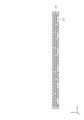
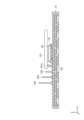
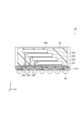
図1を参照しながら第1実施形態における半導体装置2について説明する。図1は、半導体装置2の断面図である。図1に示されるように、半導体装置2は、配線基板21と、第1半導体チップ22と、第2半導体チップ231,232,233,234と、柱状電極241,242,243,244と、モールド樹脂層25と、金属ボール26と、を備えている。The
配線基板21上に、第1半導体チップ22がフリップチップ実装されている。第1半導体チップ22は、例えばNAND型フラッシュメモリのメモリチップ、又は任意のLSIを搭載した半導体チップでもよい。第1半導体チップ22は、第1金属バンプ27を介して配線基板21に実装されている。The
第1半導体チップ22と配線基板21との間に、第1樹脂層28が設けられている。第1樹脂層28は、アンダーフィル材(UF)である。第1半導体チップ22上に、第2半導体チップ231が設けられている。第1半導体チップ22と第2半導体チップ231との間に第2樹脂層29が設けられている。A
第2半導体チップ231上に、第2半導体チップ232がずらして設けられている。第2半導体チップ231と第2半導体チップ232との間には、第3樹脂層33が設けられている。第3樹脂層33は、ダイアタッチフィルム(DAF)である。The
第2半導体チップ232上に、第2半導体チップ233がずらして設けられている。第2半導体チップ232と第2半導体チップ233との間には、第3樹脂層33が設けられている。第2半導体チップ233上に、第2半導体チップ234がずらして設けられている。第2半導体チップ233と第2半導体チップ234との間には、第3樹脂層33が設けられている。The
第2半導体チップ231の配線基板21に向かう面には、第2金属バンプ231bが設けられている。第2半導体チップ232の配線基板21に向かう面には、第2金属バンプ232bが設けられている。第2半導体チップ233の配線基板21に向かう面には、第2金属バンプ233bが設けられている。第2半導体チップ234の配線基板21に向かう面には、第2金属バンプ234bが設けられている。The
配線基板21上には、柱状電極241,242,243,244が設けられている。柱状電極241,242,243,244は、配線基板21から直立しているワイヤを含んでいる。
柱状電極241は、第2半導体チップ231の第2金属バンプ231bが設けられている位置に対応して設けられている。柱状電極241の先端は、第2金属バンプ231b内に差し込まれている。柱状電極242は、第2半導体チップ232の第2金属バンプ232bが設けられている位置に対応して設けられている。柱状電極242の先端は、第2金属バンプ232b内に差し込まれている。The
柱状電極243は、第2半導体チップ233の第2金属バンプ233bが設けられている位置に対応して設けられている。柱状電極243の先端は、第2金属バンプ233b内に差し込まれている。柱状電極244は、第2半導体チップ234の第2金属バンプ234bが設けられている位置に対応して設けられている。柱状電極244の先端は、第2金属バンプ234b内に差し込まれている。The
配線基板21上には、モールド樹脂層25が設けられている。モールド樹脂層25は、第1半導体チップ22、第2半導体チップ231,232,233,234、及び柱状電極241,242,243,244を覆っている。A molded
配線基板21の第1半導体チップ22が実装されている面と反対側の面には、金属ボール26が設けられている。
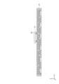
本明細書では、配線基板21等の表面に平行で互いに垂直な方向をX方向及びY方向とし、配線基板21等の表面に垂直な方向をZ方向として示している。本明細書では、+Z方向を上方向として取り扱い、-Z方向を下方向として取り扱う。例えば、第1半導体チップ22は、配線基板21の上方に位置し、第2半導体チップ231の下方に位置している。-Z方向は、重力方向と一致していても一致していなくてもよい。In this specification, directions parallel to and perpendicular to the surface of the
続いて、図2から図12を参照しながら、半導体装置2の製造方法について説明する。図2に示されるように、配線基板21を準備する。配線基板21の内部には、配線層211が設けられている。Next, a method for manufacturing the
続いて、図3に示されるように、第1半導体チップ22に第1金属バンプ27を形成する。第1半導体チップ22は、第1金属バンプ27を介して配線基板21上に形成されたパッド(不図示)とフリップチップ実装される。第1金属バンプ27としては、Sn、Ag、Cu、Au、Pd、Bi、Zn、Ni、Sb、In、Geの単体、それらの内の2種以上の複合膜、または合金を使用する。フリップチップ実装は、フラックスを使用してリフローしてもよいし、熱圧着で形成してもよい。還元雰囲気中でリフローしてもよい。FCボンダーで仮圧着後、レーザーリフローで加圧しながら加熱して接続してもよい。Next, as shown in FIG. 3, first metal bumps 27 are formed on the
続いて、図4に示されるように、第1樹脂を配線基板21と第1半導体チップ22との間に流し込み、第1樹脂層28を形成する。第1樹脂層28を形成する第1樹脂としては、フェノール系、ポリイミド系、ポリアミド系、アクリル系、エポキシ系、PBO(p-phenylenebenzobisoxazole)系、シリコーン系、ベンゾシクロブテン系等の樹脂、または、これらの混合材料、複合材料等を使用する。NCP(Non Conductive Paste)やNCF(Non Conductive Film)などを使用し、フリップチップ実装と樹脂封止とを一括で行ってもよい。Next, as shown in FIG. 4, the first resin is poured between the
続いて、図5に示されるように、配線基板21上に、柱状電極241,242,243,244を設ける。柱状電極241,242,243,244の材料としては、Cu、Ni、W、Au、Ag、Pd、Sn、Bi、Zn、Cr、Al、Ti等の単体、それらのうち2種以上の複合材料、または、それらのうち2種以上の合金等を使用する。より望ましくは、柱状電極241,242,243,244の材料としては、Au、Ag、Cu、CuPdを用いることができる。さらに望ましくは硬い材料である、Cu、CuPdを柱状電極241,242,243,244の材料として用いることができる。柱状電極241,242,243,244の材料としては、CuにPdが被覆された金属でもよい。樹脂形成時に柱状電極が倒れにくくなる。Next, as shown in FIG. 5,
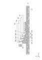
続いて、図6を参照しながら、柱状電極241,242,243,244を形成する方法について詳細に説明する。図6では、柱状電極241の形成を例にとって説明する。図6は、柱状電極241を形成する工程を(A)、(B)、(C)、(D)、(E)、(F)、(G)、(H)の順に示している。Next, a method for forming the
図6(A)に示されるように、ワイヤクランプ42から繰り出されたワイヤ241bをキャピラリ41で保持する。キャピラリ41で保持したワイヤ241bの先端をボール形状に加工し、先端部241aを形成する。配線基板21上には、電極パッド212が設けられている。電極パッド212には、Al、Cu、Au、Ni、Pdなどの単体、複合膜、合金などを用いる。As shown in FIG. 6(A), the
続いて、図6(B)に示されるように、キャピラリ41及びワイヤクランプ42を電極パッド212上に移動し、電極パッド212の直上に先端部241aを配置する。続いて、図6(C)に示されるように、キャピラリ41及びワイヤクランプ42を降下させ、先端部241aを電極パッド212に当接させる。先端部241aを電極パッド212に押し付けた状態で超音波を印加し、先端部241aを電極パッド212に接着させる。Next, as shown in FIG. 6(B), the capillary 41 and
続いて、図6(D)に示されるように、最終的に柱状電極となった場合の狙い高さに応じてワイヤ241bをキャピラリ41及びワイヤクランプ42から繰り出す。続いて、図6(E)に示されるように、キャピラリ41を電極パッド212の中心から所定位置に押し付ける。所定位置は、最終的に柱状電極となった場合の狙い高さの50―90%の位置に定められる。最終的に柱状電極となった場合の高さを安定させるため、所定位置は一定位置とした方がよい。Next, as shown in FIG. 6(D), the
続いて、図6(F)に示されるように、キャピラリ41及びワイヤクランプ42を引き上げて、ワイヤ241bを直立させる。図6(G)に示されるように、更にキャピラリ41及びワイヤクランプ42を引き上げると、図6(E)でキャピラリ41を押し付けた位置Aでワイヤ241bが切断される。最終的に、図6(H)に示されるように、切断されたワイヤ241b及び先端部241aを含む柱状電極241が形成される。Next, as shown in FIG. 6(F), the capillary 41 and
続いて、図7に示されるように、電極パッド231aが形成された第2半導体チップ231を準備する。電極パッド231aにはAl、Cu、Au、Ni、Pdなどの単体、複合膜、合金などを用いる。図には明示しないが、同様に電極パッドが形成された第2半導体チップ232,233,234を準備する。Next, as shown in FIG. 7, a
続いて、図8に示されるように、電極パッド231a上に第2金属バンプ231bを形成する。図には明示しないが、同様に第2半導体チップ232,233,234の電極パッド上に第2金属バンプ232b,233b,234bを形成する。第2金属バンプ231b,232b,233b,234bとしては、Sn、Ag、Cu、Au、Pd、Bi、Zn、Ni、Sb、In、Geの単体、それらの内の2種以上の複合膜、または合金を使用する。Next, as shown in FIG. 8,
続いて、図9に示されるように、第1半導体チップ22の裏面に第2樹脂層29を形成する。第2樹脂層29を形成する第2樹脂としては、フェノール系、ポリイミド系、ポリアミド系、アクリル系、エポキシ系、PBO(p-phenylenebenzobisoxazole)系、シリコーン系、ベンゾシクロブテン系等の樹脂、または、これらの混合材料、複合材料等を使用する。第2樹脂は液状のものを塗布して第2樹脂層29としてもよい。第2樹脂はフィルム状のものを貼り付けて第2樹脂層29としてもよい。Next, as shown in FIG. 9, a
続いて、図10に示されるように、第2樹脂層29に第2半導体チップ231を搭載する。図7及び図8を参照しながら説明したように、第2半導体チップ231には、第2金属バンプ231bが形成されている。第2樹脂層29に第2半導体チップ231を搭載する際に、柱状電極241の先端と第2金属バンプ231bとを接続する。柱状電極241の先端と第2金属バンプ231bとの接続にあたっては、例えば、フラックスを第2金属バンプ231bに塗布して、搭載後、リフローにより接続してもよいし、FCボンダーで熱圧着してもよい。還元雰囲気中にリフローしてもよい。FCボンダーで仮圧着後、レーザーリフローで加圧しながら加熱して接続してもよい。Next, as shown in FIG. 10, the
続いて、図11に示されるように、第2半導体チップ231上に第3樹脂層33を形成する。第3樹脂層33を形成する第3樹脂としては、フェノール系、ポリイミド系、ポリアミド系、アクリル系、エポキシ系、PBO(p-phenylenebenzobisoxazole)系、シリコーン系、ベンゾシクロブテン系等の樹脂、または、これらの混合材料、複合材料等を使用する。第3樹脂は液状のものを塗布して第3樹脂層33としてもよい。第3樹脂はフィルム状のものを貼り付けて第3樹脂層33としてもよい。Next, as shown in FIG. 11, a
第2半導体チップ231上に形成された第3樹脂層33に第2半導体チップ232を搭載する。第2半導体チップ232には、第2金属バンプ232bが形成されている。第2半導体チップ232を搭載するにあたっては、第2金属バンプ232bが柱状電極242に対応する位置にくるようにずらして配置する。第3樹脂層33に第2半導体チップ232を搭載する際に、柱状電極242の先端と第2金属バンプ232bとを接続する。柱状電極242の先端と第2金属バンプ232bとの接続にあたっては、例えば、フラックスを第2金属バンプ232bに塗布して、搭載後、リフローにより接続してもよいし、FCボンダーで熱圧着してもよい。還元雰囲気中にリフローしてもよい。FCボンダーで仮圧着後、レーザーリフローで加圧しながら加熱して接続してもよい。The
第2半導体チップ232上に第3樹脂層33を形成する。第3樹脂層33の材料や形成手法は上記説明した通りである。第2半導体チップ232上に形成された第3樹脂層33に第2半導体チップ233を搭載する。第2半導体チップ233を搭載するにあたっては、第2金属バンプ233bが柱状電極243に対応する位置にくるようにずらして配置する。第3樹脂層33に第2半導体チップ233を搭載する際に、柱状電極243の先端と第2金属バンプ233bとを接続する。柱状電極243の先端と第2金属バンプ233bとの接続手法は上記説明した通りである。The
第2半導体チップ233上に第3樹脂層33を形成する。第3樹脂層33の材料や形成手法は上記説明した通りである。第2半導体チップ233上に形成された第3樹脂層33に第2半導体チップ234を搭載する。第2半導体チップ234を搭載するにあたっては、第2金属バンプ234bが柱状電極244に対応する位置にくるようにずらして配置する。第3樹脂層33に第2半導体チップ234を搭載する際に、柱状電極244の先端と第2金属バンプ234bとを接続する。柱状電極244の先端と第2金属バンプ234bとの接続手法は上記説明した通りである。The
続いて、図12に示されるように、モールド樹脂層25を形成する。モールド樹脂層25は、第1半導体チップ22、第2半導体チップ231,232,233,234、及び柱状電極241,242,243,244を覆うように設けられる。モールド樹脂層25を形成するモールド樹脂としては、エポキシ系、フェノール系、ポリイミド系、ポリアミド系、アクリル系、PBO系、シリコーン系、ベンゾシクロブテン系などの樹脂、これらの混合材料、複合材料を使用する。エポキシ樹脂の例としては特に限定されず、例えば、ビスフェノールA型、ビスフェノールF型、ビスフェノールAD型、ビスフェノールS型等のビスフェノール型エポキシ樹脂、フェノールノボラック型、クレゾールノボラック型等のノボラック型エポキシ樹脂、レゾルシノール型エポキシ樹脂、トリスフェノールメタントリグリシジルエーテル等の芳香族エポキシ樹脂、ナフタレン型エポキシ樹脂、フルオレン型エポキシ樹脂、ジシクロペンタジエン型エポキシ樹脂、ポリエーテル変性エポキシ樹脂、ベンゾフェノン型エポキシ樹脂、アニリン型エポキシ樹脂、NBR変性エポキシ樹脂、CTBN変性エポキシ樹脂、及び、これらの水添化物等が挙げられる。なかでも、Siとの密着性が良い点から、ナフタレン型エポキシ樹脂、ジシクロペンタジエン型エポキシ樹脂が好ましい。また、速硬化性が得られやすいことから、ベンゾフェノン型エポキシ樹脂も好ましい。これらのエポキシ樹脂は、単独で用いられてもよく、2種以上が併用されてもよい。またモールド樹脂の中にシリカなどのフィラーが含まれていてもよい。次に、モールド樹脂をオーブン等による加熱や、UV硬化樹脂の場合、UV光をあてて硬化させる。12, the molded
続いて、図1に示されるように、配線基板21の裏面に金属ボール26を形成し、ダイシングにより個片化することで半導体装置2が完成する。金属ボール26としては、Sn、Ag、Cu、Au、Pd、Bi、Zn、Ni、Sb、In、Geの単体、それらの内の2種以上の複合膜、または合金を使用する。Next, as shown in FIG. 1,
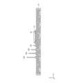
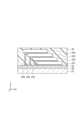
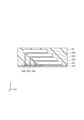
図13を参照しながら、半導体装置2における配線基板21及び第2半導体チップ231,232,233,234の配置態様について説明する。図13は、半導体装置2をZ方向に見通す平面図である。図1から図12を参照しながら説明したように、第2半導体チップ231,232,233,234は、X方向にずれて配置され、第2金属バンプ231b,232b,233b,234bが配線基板21に対向できるようになっている。一方、第2半導体チップ231,232,233,234は、Y方向にはずれておらず、X方向に沿った辺が揃うように配置されている。With reference to FIG. 13, the arrangement of the
上述の工程に従って、半導体装置2を製造し、配線基板上に搭載して、温度サイクル試験に供して、その信頼性を調べた。なお温度サイクル試験は-55℃(30min)~25℃(5min)~125℃(30min)を1サイクルとして行った。その結果3000サイクル後でも接続箇所には破断の発生は全く認められなかった。The
従来のような半導体チップに柱状電極を形成しているのに比べ、配線基板21上に柱状電極241,242,243,244を形成しているため、第2半導体チップ231,232,233,234へのダメージは発生しない。Compared to the conventional method of forming columnar electrodes on a semiconductor chip,
柱状電極241,242,243,244としてワイヤを例にしたが、めっき法などで形成してもよい。ワイヤ法とめっき法が混在してもよい。もちろん通常のワイヤボンディング法を用いた製品のように、チップ間を直接接続するワイヤと、ワイヤを使用した柱状電極が混在していてもよい。チップ間を直接接続するワイヤと、めっき法などを使用した柱状電極が混在していてもよい。チップ間を直接接続するワイヤと、ワイヤを用いた柱状電極、めっき法などを適用した柱状電極が混在してもよい。Wires are used as an example of the
また第2樹脂層29は形成せずに、第2半導体チップ231を配線基板21上に搭載してもよい。その場合は、モールド樹脂層25が第1半導体チップ22の裏面と第2半導体チップ231の間に形成される。The
また第1半導体チップ22がNAND型フラッシュメモリ、第2半導体チップ231がコントローラチップでもよい。The
図14から図17を参照しながら、変形例である半導体装置2A(図17参照)の製造方法について説明する。図14に示されるように、支持板30を準備する。支持板30としては、シリコン、ガラス、セラミック、樹脂板、リードフレーム等の金属板などを使用する。支持板30が配線基板21に向かう方の面に、第3樹脂層33を介して第2半導体チップ234を設ける。第3樹脂層33を構成する第3樹脂は、フェノール系、ポリイミド系、ポリアミド系、アクリル系、エポキシ系、PBO(p-phenylenebenzobisoxazole)系、シリコーン系、ベンゾシクロブテン系等の樹脂、または、これらの混合材料、複合材料等を使用する。第3樹脂層33は支持板30側に形成してもよいし、第2半導体チップ234の裏面に形成してもよい。With reference to Figs. 14 to 17, a manufacturing method of the
第2半導体チップ234に設けられている第2金属バンプ234bが露出するようにずらし、第3樹脂層33を介して第2半導体チップ233を配置する。第2半導体チップ233に設けられている第2金属バンプ233bが露出するようにずらし、第3樹脂層33を介して第2半導体チップ232を配置する。第2半導体チップ232に設けられている第2金属バンプ232bが露出するようにずらし、第3樹脂層33を介して第2半導体チップ231を配置する。The
図15に示されるように、図9を参照しながら説明した配線基板21を準備する。この配線基板21には、第1半導体チップ22、柱状電極241,242,243,244等が設けられている。図14を参照しながら説明した、支持板30及び第2半導体チップ231,232,233,234を配線基板21上に搭載する。第2半導体チップ231と第1半導体チップ22とは、第2樹脂層29を介して接着される。第2樹脂層29を構成する第2樹脂としては、フェノール系、ポリイミド系、ポリアミド系、アクリル系、エポキシ系、PBO(p-phenylenebenzobisoxazole)系、シリコーン系、ベンゾシクロブテン系等の樹脂、または、これらの混合材料、複合材料等を使用する。As shown in FIG. 15, the
第2金属バンプ231b,232b,233b,234bと、柱状電極241,242,243,244の先端とが接続される。例えば、フラックスを第2金属バンプ231b,232b,233b,234bに塗布して、搭載後、リフローにより接続してもよいし、FCボンダーで熱圧着してもよい。還元雰囲気中にリフローしてもよい。FCボンダーで仮圧着後、レーザーリフローで加圧しながら加熱して接続してもよい。The second metal bumps 231b, 232b, 233b, and 234b are connected to the tips of the
続いて、図16に示されるように、モールド樹脂層25を形成する。モールド樹脂層25は、第1半導体チップ22、第2半導体チップ231,232,233,234、柱状電極241,242,243,244、及び支持板30を覆うように設けられる。モールド樹脂層25を形成するモールド樹脂としては、エポキシ系、フェノール系、ポリイミド系、ポリアミド系、アクリル系、PBO系、シリコーン系、ベンゾシクロブテン系などの樹脂、これらの混合材料、複合材料を使用する。エポキシ樹脂の例としては特に限定されず、例えば、ビスフェノールA型、ビスフェノールF型、ビスフェノールAD型、ビスフェノールS型等のビスフェノール型エポキシ樹脂、フェノールノボラック型、クレゾールノボラック型等のノボラック型エポキシ樹脂、レゾルシノール型エポキシ樹脂、トリスフェノールメタントリグリシジルエーテル等の芳香族エポキシ樹脂、ナフタレン型エポキシ樹脂、フルオレン型エポキシ樹脂、ジシクロペンタジエン型エポキシ樹脂、ポリエーテル変性エポキシ樹脂、ベンゾフェノン型エポキシ樹脂、アニリン型エポキシ樹脂、NBR変性エポキシ樹脂、CTBN変性エポキシ樹脂、及び、これらの水添化物等が挙げられる。なかでも、Siとの密着性が良い点から、ナフタレン型エポキシ樹脂、ジシクロペンタジエン型エポキシ樹脂が好ましい。また、速硬化性が得られやすいことから、ベンゾフェノン型エポキシ樹脂も好ましい。これらのエポキシ樹脂は、単独で用いられてもよく、2種以上が併用されてもよい。またモールド樹脂の中にシリカなどのフィラーが含まれていてもよい。次に、モールド樹脂をオーブン等による加熱や、UV硬化樹脂の場合、UV光をあてて硬化させる。16, the molded
続いて、図17に示されるように、配線基板21の裏面に金属ボール26を形成し、ダイシングにより個片化することで半導体装置2Aが完成する。金属ボール26としては、Sn、Ag、Cu、Au、Pd、Bi、Zn、Ni、Sb、In、Geの単体、それらの内の2種以上の複合膜、または合金を使用する。Next, as shown in FIG. 17,
上述の工程に従って、半導体装置2Aを製造し、配線基板上に搭載して、温度サイクル試験に供して、その信頼性を調べた。なお温度サイクル試験は-55℃(30min)~25℃(5min)~125℃(30min)を1サイクルとして行った。その結果3000サイクル後でも接続箇所には破断の発生は全く認められなかった。The
従来のような半導体チップに柱状電極を形成しているのに比べ、配線基板21上に柱状電極241,242,243,244を形成しているため、第2半導体チップ231,232,233,234へのダメージは発生しない。Compared to the conventional method of forming columnar electrodes on a semiconductor chip,
柱状電極241,242,243,244としてワイヤを例にしたが、めっき法などで形成してもよい。ワイヤ法とめっき法が混在してもよい。もちろん通常のワイヤボンディング法を用いた製品のように、チップ間を直接接続するワイヤと、ワイヤを使用した柱状電極が混在していてもよい。チップ間を直接接続するワイヤと、めっき法などを使用した柱状電極が混在していてもよい。チップ間を直接接続するワイヤと、ワイヤを用いた柱状電極、めっき法などを適用した柱状電極が混在してもよい。Wires are used as an example of the
また第2樹脂層29は形成せずに、第2半導体チップ231を配線基板21上に搭載してもよい。その場合は、モールド樹脂層25が第1半導体チップ22の裏面と第2半導体チップ231の間に形成される。The
また第1半導体チップ22がNAND型フラッシュメモリ、第2半導体チップ231がコントローラチップでもよい。The
図18を参照しながら、変形例である半導体装置について説明する。図18は、第1実施形態を説明した図11に対応する図である。図11に示される第1実施形態との相違点は、第2金属バンプ231b,232b,233b,234bに代えて、ピラーバンプ231c,232c,233c,234c及び低融点金属部231d,232d,233d,234dを設けている点である。A modified semiconductor device will be described with reference to FIG. 18. FIG. 18 is a diagram corresponding to FIG. 11 which describes the first embodiment. The difference from the first embodiment shown in FIG. 11 is that pillar bumps 231c, 232c, 233c, 234c and low melting
第2半導体チップ231に、ピラーバンプ231cを形成し、その後ピラーバンプ231c上に低融点金属部231dを形成する。同様に、第2半導体チップ232に、ピラーバンプ232cを形成し、その後ピラーバンプ232c上に低融点金属部232dを形成する。第2半導体チップ233に、ピラーバンプ233cを形成し、その後ピラーバンプ233c上に低融点金属部233dを形成する。第2半導体チップ234に、ピラーバンプ234cを形成し、その後ピラーバンプ234c上に低融点金属部234dを形成する。Pillar bumps 231c are formed on the
ピラーバンプ231c,232c,233c,234cとしては、Ag、Cu、Au、Pd、Niの単体、それらの内の2種以上の複合膜、または合金を使用する。低融点金属部231d,232d,233d,234dとしては、Sn、Ag、Cu、Au、Pd、Bi、Zn、Ni、Sb、In、Geの単体、それらの内の2種以上の複合膜、または合金を使用する。For the pillar bumps 231c, 232c, 233c, and 234c, Ag, Cu, Au, Pd, and Ni alone, or a composite film of two or more of these, or an alloy is used. For the low melting
ピラーバンプ231c,232c,233c,234cを形成することにより、柱状電極241,242,243,244との接続部を第2半導体チップ231,232,233,234のチップ面から離すことができる。接続部をチップ面から離すことで、第2半導体チップ231,232,233,234と配線基板21との熱膨張係数差に起因して接続部にかかる歪の影響が小さくなり、信頼性がより向上する。ピラーバンプや柱状電極の間隔を狭くする狭ピッチ化にも対応可能となる。また、柱状電極241,242,243,244の径に対して、ピラーバンプ231c,232c,233c,234cの径を大きくすることにより、各部に生じる応力を小さくすることができる。By forming the pillar bumps 231c, 232c, 233c, and 234c, the connection parts with the
図19を参照しながら、変形例である半導体装置について説明する。図19は、第1実施形態を説明した図11に対応する図である。図11に示される第1実施形態との相違点は、柱状電極241,242,243,244と配線基板21の電極パッド211との接続部を覆うように第4樹脂層31を設ける点である。A modified semiconductor device will be described with reference to FIG. 19. FIG. 19 is a diagram corresponding to FIG. 11 which describes the first embodiment. The difference from the first embodiment shown in FIG. 11 is that a
第4樹脂層31を形成する第4樹脂としては、エポキシ系、フェノール系、ポリイミド系、ポリアミド系、アクリル系、PBO系、シリコーン系、ベンゾシクロブテン系などの樹脂、これらの混合材料、複合材料を使用する。第4樹脂層31を形成することにより、モールド樹脂層25を形成時の柱状電極241,242,243,244の倒れを抑制することが可能となり、信頼性が向上する。The fourth resin used to form the
図20を参照しながら、変形例である半導体装置について説明する。図20は、第1実施形態を説明した図11に対応する図である。図11に示される第1実施形態との相違点は、配線基板21の柱状電極が設けられる部分に段差部32が設けられている点である。段差部32は、第2半導体チップ232,233,234によって形成される段差に応じて設けられている。段差部32は、第1段322、第2段323、及び第3段324を有している。第1段322の内部には、内部配線322aが設けられている。第2段323の内部には、内部配線323aが設けられている。第3段324の内部には、内部配線324aが設けられている。図には明示しないが、第1段322の表面には、内部配線322aに繋がる電極パッドが設けられている。同様に、第2段323の表面には、内部配線323aに繋がる電極パッドが設けられている。第3段324の表面には、内部配線324aに繋がる電極パッドが設けられている。With reference to FIG. 20, a semiconductor device as a modified example will be described. FIG. 20 is a view corresponding to FIG. 11 in which the first embodiment is described. The difference from the first embodiment shown in FIG. 11 is that a
配線基板21上には、柱状電極241Dが設けられている。柱状電極241Dは、第2半導体チップ231に設けられた第2金属バンプ231bに繋がっている。第1段322に設けられている電極パッド上には、柱状電極242Dが設けられている。柱状電極242Dは、第2半導体チップ232に設けられた第2金属バンプ232bに繋がっている。A
第2段323に設けられている電極パッド上には、柱状電極243Dが設けられている。柱状電極243Dは、第2半導体チップ233に設けられた第2金属バンプ233bに繋がっている。第3段324に設けられている電極パッド上には、柱状電極244Dが設けられている。柱状電極244Dは、第2半導体チップ234に設けられた第2金属バンプ234bに繋がっている。A
柱状電極241D,242D,243D,244Dは、全て同じ長さに形成されている。柱状電極241D,242D,243D,244Dの長さが同じになることで、電気的特性が向上する。また、積層チップ数が増えると長い柱状電極を形成する必要があるが、この方式であれば、長い柱状電極を形成する必要がなく、柱状電極の倒れを抑制することができる。The
続いて、図21から図28を参照しながら、第2実施形態における半導体装置2E(図28参照)の製造方法について説明する。図21に示されるように、ガラス支持体51、剥離層52、及び金属層53が積層されたものを準備する。剥離層52としては、エポキシ系、フェノール系、ポリイミド系、ポリアミド系、アクリル系、PBO系、シリコーン系、ベンゾシクロブテン系などの樹脂、これらの混合材料、複合材料を使用する。金属層53としては、Al、Cu、Au、Ni、Pd、Ti、Crなどの単体、複合膜、合金などを用いる。Next, a method for manufacturing the
続いて、図22に示されるように、金属層53上に柱状電極242,243,244を設ける。続いて、図23に示されるように、金属層53上に第2半導体チップ231,232,233,234を積層する。Next, as shown in FIG. 22,
金属層53上に、第3樹脂層33を介して第2半導体チップ231を設ける。第3樹脂層33を形成する第3樹脂については上記説明した通りなので、その説明を省略する。第2半導体チップ231と金属層53との間には、金属ピラー54が設けられている。金属ピラー54としては、Ag、Cu、Au、Pd、Niの単体、それらの内の2種以上の複合膜、または合金を使用する。The
第2半導体チップ231上に形成された第3樹脂層33に第2半導体チップ232を搭載する。第2半導体チップ232には、第2金属バンプ232bが形成されている。第2金属バンプ232bとしては、Sn、Ag、Cu、Au、Pd、Bi、Zn、Ni、Sb、In、Geの単体、それらの内の2種以上の複合膜、または合金を使用する。金属バンプをピラーバンプと低融点金属部の組み合わせにしてもよい。ピラーバンプとしては、Ag、Cu、Au、Pd、Niの単体、それらの内の2種以上の複合膜、または合金を使用する。低融点金属部としては、Sn、Ag、Cu、Au、Pd、Bi、Zn、Ni、Sb、In、Geの単体、それらの内の2種以上の複合膜、または合金を使用する。第2半導体チップ232を搭載するにあたっては、第2金属バンプ232bが柱状電極242に対応する位置にくるようにずらして配置する。第3樹脂層33に第2半導体チップ232を搭載する際に、柱状電極242の先端と第2金属バンプ232bとを接続する。柱状電極242の先端と第2金属バンプ232bとの接続にあたっては、例えば、フラックスを第2金属バンプ232bに塗布して、搭載後、リフローにより接続してもよいし、FCボンダーで熱圧着してもよい。還元雰囲気中にリフローしてもよい。FCボンダーで仮圧着後、レーザーリフローで加圧しながら加熱して接続してもよい。The
第2半導体チップ232上に第3樹脂層33を形成する。第3樹脂層33の材料や形成手法は上記説明した通りである。第2半導体チップ232上に形成された第3樹脂層33に第2半導体チップ233を搭載する。第2半導体チップ233を搭載するにあたっては、第2金属バンプ233bが柱状電極243に対応する位置にくるようにずらして配置する。第3樹脂層33に第2半導体チップ233を搭載する際に、柱状電極243の先端と第2金属バンプ233bとを接続する。柱状電極243の先端と第2金属バンプ233bとの接続手法は上記説明した通りである。The
第2半導体チップ233上に第3樹脂層33を形成する。第3樹脂層33の材料や形成手法は上記説明した通りである。第2半導体チップ233上に形成された第3樹脂層33に第2半導体チップ234を搭載する。第2半導体チップ234を搭載するにあたっては、第2金属バンプ234bが柱状電極244に対応する位置にくるようにずらして配置する。第3樹脂層33に第2半導体チップ234を搭載する際に、柱状電極244の先端と第2金属バンプ234bとを接続する。柱状電極244の先端と第2金属バンプ234bとの接続手法は上記説明した通りである。The
続いて、図24に示される通り、モールド樹脂層25を形成する。モールド樹脂層25は、第1半導体チップ22、第2半導体チップ231,232,233,234、及び柱状電極242,243,244を覆うように設けられる。モールド樹脂層25を形成するモールド樹脂については上記説明した通りなので、その説明を省略する。Next, as shown in FIG. 24, the molded
続いて、図25に示される通り、ガラス支持体51をレーザ剥離によって剥離する。続いて、図26に示される通り、剥離層52及び金属層53を除去する。続いて、図27に示される通り、配線基板21Eに搭載する。配線基板21Eは、例えば有機基板が用いられるがこれに限られるものではなく、再配線基板でもよい。Then, as shown in FIG. 25, the
続いて、図28に示される通り、モールド樹脂層25Eを形成する。配線基板21Eの裏面に金属ボール26を形成し、ダイシングにより個片化することで半導体装置2Eが完成する。Next, as shown in FIG. 28, a molded
続いて、図29及び図30を参照しながら、第2実施形態の変形例である半導体装置2Fについて説明する。図29は、図27に対応する図面である。図29に示される通り、配線基板21Eに代えて配線基板21Fを用いることができる。配線基板21Fは、再配線基板である。続いて、図30に示される通り、モールド樹脂層25を形成する。配線基板21Fの裏面に金属ボール26を形成し、ダイシングにより個片化することで半導体装置2Fが完成する。Next, with reference to Figures 29 and 30, a
続いて、図31から図35を参照しながら、半導体装置2Fの異なる製造方法について説明する。図31に示されるように、ガラス支持体51、剥離層52、及び配線基板21Fが積層されたものを準備する。配線基板21Fは、再配線基板である。Next, a different manufacturing method for the
続いて、図32に示されるように、配線基板21F上に柱状電極242,243,244を設ける。続いて、図33に示されるように、配線基板21F上に第2半導体チップ231,232,233,234を積層する。Next, as shown in FIG. 32,
配線基板21F上に、第3樹脂層33を介して第2半導体チップ231を設ける。第3樹脂層33を形成する第3樹脂については上記説明した通りなので、その説明を省略する。第2半導体チップ231と配線基板21Fとの間には、金属ピラー54が設けられている。The
第2半導体チップ231上に形成された第3樹脂層33に第2半導体チップ232を搭載する。第2半導体チップ232には、第2金属バンプ232bが形成されている。第2半導体チップ232を搭載するにあたっては、第2金属バンプ232bが柱状電極242に対応する位置にくるようにずらして配置する。第3樹脂層33に第2半導体チップ232を搭載する際に、柱状電極242の先端と第2金属バンプ232bとを接続する。柱状電極242の先端と第2金属バンプ232bとの接続にあたっては、例えば、フラックスを第2金属バンプ232bに塗布して、搭載後、リフローにより接続してもよいし、FCボンダーで熱圧着してもよい。還元雰囲気中にリフローしてもよい。FCボンダーで仮圧着後、レーザーリフローで加圧しながら加熱して接続してもよい。The
第2半導体チップ232上に第3樹脂層33を形成する。第3樹脂層33の材料や形成手法は上記説明した通りである。第2半導体チップ232上に形成された第3樹脂層33に第2半導体チップ233を搭載する。第2半導体チップ233を搭載するにあたっては、第2金属バンプ233bが柱状電極243に対応する位置にくるようにずらして配置する。第3樹脂層33に第2半導体チップ233を搭載する際に、柱状電極243の先端と第2金属バンプ233bとを接続する。柱状電極243の先端と第2金属バンプ233bとの接続手法は上記説明した通りである。The
第2半導体チップ233上に第3樹脂層33を形成する。第3樹脂層33の材料や形成手法は上記説明した通りである。第2半導体チップ233上に形成された第3樹脂層33に第2半導体チップ234を搭載する。第2半導体チップ234を搭載するにあたっては、第2金属バンプ234bが柱状電極244に対応する位置にくるようにずらして配置する。第3樹脂層33に第2半導体チップ234を搭載する際に、柱状電極244の先端と第2金属バンプ234bとを接続する。柱状電極244の先端と第2金属バンプ234bとの接続手法は上記説明した通りである。The
続いて、図34に示される通り、モールド樹脂層25を形成する。モールド樹脂層25は、第1半導体チップ22、第2半導体チップ231,232,233,234、及び柱状電極242,243,244を覆うように設けられる。モールド樹脂層25を形成するモールド樹脂については上記説明した通りなので、その説明を省略する。Next, as shown in FIG. 34, the molded
続いて、図35に示される通り、ガラス支持体51をレーザ剥離によって剥離する。tづいて、剥離層52を除去する。続いて、配線基板21Fの裏面に金属ボール26を形成し、ダイシングにより個片化することで半導体装置2F(図30参照)が完成する。Next, as shown in FIG. 35, the
上記説明したように、半導体装置2,2A,2E,2Fは、内部に配線層が設けられた配線基板21,21E,21Fと、配線基板21,21E,21F上に設けられた第1半導体チップ22と、第1半導体チップ22上にずらして設けられ、配線基板21,21E,21Fに対向する面に金属バンプが設けられた第2半導体チップ231,232,233,234と、配線基板21,21E,21F上に設けられ、第2半導体チップ231,232,233,234に設けられた第2金属バンプ231b,232b,233b,234bに接続されたワイヤを含む柱状電極241,242,243,244と、を備える。第2金属バンプ231b,232b,233b,234bに代えて、ピラーバンプ231c,232c,233c,234c及び低融点金属部231d,232d,233d,234dを設けてもよい。第1半導体チップ22は、配線基板21,21E,21F上にフリップチップ実装されている。As described above, the
上記説明したように、半導体装置2,2A,2E,2Fの製造方法は、内部に配線層が設けられた配線基板21,21E,21Fを準備し、配線基板21,21E,21F上に第1半導体チップ22を設け、配線基板21,21E,21F上にワイヤを含む柱状電極241,242,243,244を設け、第1半導体チップ22上にずらして第2半導体チップ231,232,233,234を設け、第2半導体チップ231,232,233,234に設けられた第2金属バンプ231b,232b,233b,234bに柱状電極241,242,243,244を接続する。第2金属バンプ231b,232b,233b,234bに代えて、ピラーバンプ231c,232c,233c,234c及び低融点金属部231d,232d,233d,234dを設けてもよい。第1半導体チップ22は、配線基板21,21E,21F上にフリップチップ実装する。As described above, the manufacturing method of the
図19を参照しながら説明したように、柱状電極241,242,243,244が配線基板21に当接する部分に樹脂部である第4樹脂層31を設けてもよい。半導体装置2の製造方法では、配線基板21上に柱状電極241,242,243,244を設け、柱状電極241,242,243,244が配線基板21に当接する部分に樹脂部である第4樹脂層31を設ける。As described with reference to FIG. 19, a
図20を参照しながら説明したように、配線基板21の表面に段差部32が設けられ、柱状電極242D,243D,244Dは段差部32上に設けられていてもよい。半導体装置2の製造方法では、内部に配線層が設けられ、表面に段差部32が設けられている配線基板21を準備し、段差部32上に柱状電極242D,243D,244Dを設ける。As described with reference to FIG. 20, a
以上、具体例を参照しつつ本実施形態について説明した。しかし、本開示はこれらの具体例に限定されるものではない。これら具体例に、当業者が適宜設計変更を加えたものも、本開示の特徴を備えている限り、本開示の範囲に包含される。前述した各具体例が備える各要素およびその配置、条件、形状などは、例示したものに限定されるわけではなく適宜変更することができる。前述した各具体例が備える各要素は、技術的な矛盾が生じない限り、適宜組み合わせを変えることができる。The present embodiment has been described above with reference to specific examples. However, the present disclosure is not limited to these specific examples. Design modifications to these specific examples made by a person skilled in the art are also included within the scope of the present disclosure as long as they have the features of the present disclosure. The elements of each of the above-mentioned specific examples, as well as their arrangement, conditions, shape, etc., are not limited to those exemplified and can be modified as appropriate. The elements of each of the above-mentioned specific examples can be combined in different ways as appropriate, as long as no technical contradictions arise.
2,2A,2E,2F:半導体装置
21,21E,21F:配線基板
211:配線層
212:電極パッド
22:第1半導体チップ
231,232,233,234:第2半導体チップ
231a:電極パッド
231b,232b,233b,234b:第2金属バンプ
231c,232c,233c,234c:ピラーバンプ
231d,232d,233d,234d:低融点金属部
241,242,243,244,242D,243D,244D:柱状電極
241a:先端部
241b:ワイヤ
25,25E:モールド樹脂層
26:金属ボール
27:第1金属バンプ
28:第1樹脂層
29:第2樹脂層
30:支持板
31:第4樹脂層
32:段差部
33:第3樹脂層
41:キャピラリ
42:ワイヤクランプ
51:ガラス支持体
52:剥離層
53:金属層
54:金属ピラー2, 2A, 2E, 2F:
Claims (8)
Translated fromJapanese内部に配線層が設けられた配線基板と、
前記配線基板上にフリップチップ接続で設けられた第1半導体チップと、
前記第1半導体チップ上にずらして設けられ、前記配線基板に対向する面に第1金属バンプが設けられた第2半導体チップと、
前記配線基板上に設けられ、前記第2半導体チップに設けられた前記第1金属バンプに接続された第1柱状電極と、
前記第2半導体チップ上にずらして設けられ、前記配線基板に対向する面に第2金属バンプが設けられた第3半導体チップと、
前記配線基板上に設けられ、前記第3半導体チップに設けられた前記第2金属バンプに接続された第2柱状電極と、
前記第1半導体チップ、前記第2半導体チップ、前記第3半導体チップ、及び前記配線基板を覆う第1樹脂と、を備え、
前記第1柱状電極は、ワイヤ状に形成されており、前記配線基板側の端部である第1端部と、前記第1端部及び前記第1金属バンプの間に設けられる第1中間部と、を有し、
前記第1中間部の径は、前記第1端部の径及び前記第1金属バンプの径よりも小さく、
前記第2柱状電極は、ワイヤ状に形成されており、前記配線基板側の端部である第2端部と、前記第2端部及び前記第2金属バンプの間に設けられる第2中間部と、を有し、
前記第2中間部の径は、前記第2端部の径及び前記第2金属バンプの径よりも小さく、
前記第2柱状電極は、前記第1柱状電極よりも長い、
半導体装置。 A semiconductor device comprising:
A wiring board having a wiring layer provided therein;
a first semiconductor chip provided on the wiring substrateby flip-chip connection ;
a second semiconductor chip provided on the first semiconductor chip and having afirst metal bump on a surface facing the wiring substrate;
a first columnar electrode provided on the wiring substrate and connected tothe first metal bump provided on the second semiconductor chip;
a third semiconductor chip provided on the second semiconductor chip and having second metal bumps on a surface facing the wiring substrate;
a second columnar electrode provided on the wiring substrate and connected to the second metal bump provided on the third semiconductor chip;
a first resin covering the first semiconductor chip, the second semiconductor chip, the third semiconductor chip, and the wiring substrate;
the first pillar-shaped electrode is formed in a wire shape and has a first end portion which is an end portion on the wiring substrate side, and a first intermediate portion provided between the first end portion and the first metal bump,
a diameter of the first intermediate portion is smaller than a diameter of the first end portion and a diameter of the first metal bump;
the second pillar electrode is formed in a wire shape and has a second end portion which is an end portion on the wiring substrate side, and a second intermediate portion provided between the second end portion and the second metal bump,
a diameter of the second intermediate portion is smaller than a diameter of the second end portion and a diameter of the second metal bump;
The second columnar electrode is longer than the first columnar electrode.
Semiconductor device.
前記第1半導体チップと前記配線基板との間に設けられ、前記第1樹脂と異なる第2樹脂を更に備える、半導体装置。 2. The semiconductor device according to claim 1,
the semiconductor devicefurther comprising a second resin provided between the first semiconductor chip and the wiring substrate, the second resin being different from the first resin .
前記第1柱状電極の前記第1端部、及び前記第2柱状電極の前記第2端部を覆うように設けられ、前記第1樹脂及び前記第2樹脂と異なる第3樹脂を更に備える、半導体装置。 3. The semiconductor device according to claim2 ,
the semiconductor devicefurther comprising a third resin different from the first resin and the second resin, the third resin being provided so as to cover the first end of the first columnar electrode and the second end of the second columnar electrode .
前記第3半導体チップ上に設けられる支持板を更に備える、半導体装置。 The semiconductor device according toany one of claims 1 to 3 ,
The semiconductor devicefurther comprises a support plate provided on the third semiconductor chip .
内部に配線層が設けられた配線基板を準備し、
前記配線基板上に第1半導体チップをフリップチップにより設け、
前記配線基板上にワイヤボンディングにより第1柱状電極を設け、
前記配線基板上にワイヤボンディングにより、前記第1柱状電極よりも長い第2柱状電極を設け、
第2半導体チップに第1金属バンプを設け、
第3半導体チップに第2金属バンプを設け、
前記第1半導体チップ上にずらして前記第2半導体チップを設け、前記第1金属バンプに前記第1柱状電極を接続し、
前記第2半導体チップ上にずらして前記第3半導体チップを設け、前記第2金属バンプに前記第2柱状電極を接続し、
前記第1半導体チップ、前記第2半導体チップ、前記第3半導体チップ、及び前記配線基板を覆うように第1樹脂を形成し、
ここで、
前記第1柱状電極は、前記配線基板側の端部である第1端部と、前記第1端部及び前記第1金属バンプの間に設けられる第1中間部と、を有し、
前記第1中間部の径は、前記第1端部の径及び前記第1金属バンプの径よりも小さく、
前記第2柱状電極は、前記配線基板側の端部である第2端部と、前記第2端部及び前記第2金属バンプの間に設けられる第2中間部と、を有し、
前記第2中間部の径は、前記第2端部の径及び前記第2金属バンプの径よりも小さい、
半導体装置の製造方法。 A method for manufacturing a semiconductor device, comprising:
A wiring board having a wiring layer provided therein is prepared;
a first semiconductor chip is provided on the wiring substrateby flip chip mounting ;
providinga first columnar electrode on the wiring board by wire bonding ;
providing a second columnar electrode longer than the first columnar electrode on the wiring board by wire bonding;
providing a first metal bump on the second semiconductor chip;
providing a second metal bump on the third semiconductor chip;
the second semiconductor chip is provided onthe first semiconductor chip in a shifted manner, andthe firstcolumnar electrodesare connected to the first metal bumps;
the third semiconductor chip is provided on the second semiconductor chip in a shifted manner, and the second columnar electrodes are connected to the second metal bumps;
forming a first resin so as to cover the first semiconductor chip, the second semiconductor chip, the third semiconductor chip, and the wiring substrate;
Where:
the first pillar-shaped electrode has a first end portion which is an end portion on the wiring substrate side, and a first intermediate portion provided between the first end portion and the first metal bump,
a diameter of the first intermediate portion is smaller than a diameter of the first end portion and a diameter of the first metal bump;
the second columnar electrode has a second end portion which is an end portion on the wiring substrate side, and a second intermediate portion provided between the second end portion and the second metal bump,
a diameter of the second intermediate portion is smaller than a diameter of the second end portion and a diameter of the second metal bump;
A method for manufacturing a semiconductor device.
前記第1半導体チップと前記配線基板との間に前記第1樹脂と異なる第2樹脂を設ける、半導体装置の製造方法。 6. The method for manufacturing a semiconductor device according to claim 5,
A method for manufacturing a semiconductor device, comprising:providing a second resin different from the first resin between the first semiconductor chip and the wiring substrate .
前記第1柱状電極の前記第1端部、及び前記第2柱状電極の前記第2端部を覆うように、前記第1樹脂及び前記第2樹脂と異なる第3樹脂を設ける、半導体装置の製造方法。 7. A method for manufacturing a semiconductor device according to claim6 , comprising the steps of:
a third resin different from the first resin and the second resin provided so as to cover the first end of the first columnar electrode and the second end of the second columnar electrode.
前記第3半導体チップ上に支持板を設ける、半導体装置の製造方法。 A method for manufacturing a semiconductor device according toany one of claims 5 to 7 , comprising the steps of:
providing a support plate on the third semiconductor chip .
Priority Applications (4)
| Application Number | Priority Date | Filing Date | Title |
|---|---|---|---|
| JP2021154454AJP7703411B2 (en) | 2021-09-22 | 2021-09-22 | Semiconductor device and method for manufacturing the same |
| TW111105361ATWI819491B (en) | 2021-09-22 | 2022-02-15 | Semiconductor device and method of manufacturing semiconductor device |
| CN202210149707.3ACN115863284A (en) | 2021-09-22 | 2022-02-18 | Semiconductor device and method for manufacturing semiconductor device |
| US17/681,487US20230089223A1 (en) | 2021-09-22 | 2022-02-25 | Semiconductor device and method for manufacturing semiconductor device |
Applications Claiming Priority (1)
| Application Number | Priority Date | Filing Date | Title |
|---|---|---|---|
| JP2021154454AJP7703411B2 (en) | 2021-09-22 | 2021-09-22 | Semiconductor device and method for manufacturing the same |
Publications (2)
| Publication Number | Publication Date |
|---|---|
| JP2023045852A JP2023045852A (en) | 2023-04-03 |
| JP7703411B2true JP7703411B2 (en) | 2025-07-07 |
Family
ID=85572369
Family Applications (1)
| Application Number | Title | Priority Date | Filing Date |
|---|---|---|---|
| JP2021154454AActiveJP7703411B2 (en) | 2021-09-22 | 2021-09-22 | Semiconductor device and method for manufacturing the same |
Country Status (4)
| Country | Link |
|---|---|
| US (1) | US20230089223A1 (en) |
| JP (1) | JP7703411B2 (en) |
| CN (1) | CN115863284A (en) |
| TW (1) | TWI819491B (en) |
Families Citing this family (1)
| Publication number | Priority date | Publication date | Assignee | Title |
|---|---|---|---|---|
| JP2023141098A (en) | 2022-03-23 | 2023-10-05 | キオクシア株式会社 | Semiconductor device |
Citations (9)
| Publication number | Priority date | Publication date | Assignee | Title |
|---|---|---|---|---|
| JP2001014218A (en) | 1999-06-30 | 2001-01-19 | Hitachi Ltd | Memory module and memory system |
| JP2011119756A (en) | 2004-05-20 | 2011-06-16 | Toshiba Corp | Stacked electronic component |
| WO2012111814A1 (en) | 2011-02-18 | 2012-08-23 | 古河電気工業株式会社 | Wiring substrate, method for manufacturing same, and semiconductor device |
| JP2016535463A (en) | 2014-10-03 | 2016-11-10 | インテル コーポレイション | Overlapping stacked die package with vertical columns |
| US20180204821A1 (en) | 2015-09-23 | 2018-07-19 | Intel Corporation | Substrates, assembles, and techniques to enable multi-chip flip chip packages |
| US20180211936A1 (en) | 2017-01-25 | 2018-07-26 | Powertech Technology Inc. | Thin fan-out multi-chip stacked package structure and manufacturing method thereof |
| US20190067248A1 (en) | 2017-08-24 | 2019-02-28 | Micron Technology, Inc. | Semiconductor device having laterally offset stacked semiconductor dies |
| US20190229093A1 (en) | 2016-10-01 | 2019-07-25 | Intel Corporation | Electronic device package |
| CN112956023A (en) | 2021-02-05 | 2021-06-11 | 长江存储科技有限责任公司 | Flip chip stacking structure and forming method thereof |
Family Cites Families (6)
| Publication number | Priority date | Publication date | Assignee | Title |
|---|---|---|---|---|
| US8089142B2 (en)* | 2002-02-13 | 2012-01-03 | Micron Technology, Inc. | Methods and apparatus for a stacked-die interposer |
| TWI378545B (en)* | 2008-12-16 | 2012-12-01 | Powertech Technology Inc | Chip stacked package having single-sided pads on chips |
| JP5561190B2 (en)* | 2011-01-31 | 2014-07-30 | 富士通株式会社 | Semiconductor device, semiconductor device manufacturing method, and electronic device |
| US8878353B2 (en)* | 2012-12-20 | 2014-11-04 | Invensas Corporation | Structure for microelectronic packaging with bond elements to encapsulation surface |
| US10276545B1 (en)* | 2018-03-27 | 2019-04-30 | Powertech Technology Inc. | Semiconductor package and manufacturing method thereof |
| TWI700798B (en)* | 2018-07-12 | 2020-08-01 | 南韓商三星電子股份有限公司 | Semiconductor package |
- 2021
- 2021-09-22JPJP2021154454Apatent/JP7703411B2/enactiveActive
- 2022
- 2022-02-15TWTW111105361Apatent/TWI819491B/enactive
- 2022-02-18CNCN202210149707.3Apatent/CN115863284A/enactivePending
- 2022-02-25USUS17/681,487patent/US20230089223A1/enactivePending
Patent Citations (9)
| Publication number | Priority date | Publication date | Assignee | Title |
|---|---|---|---|---|
| JP2001014218A (en) | 1999-06-30 | 2001-01-19 | Hitachi Ltd | Memory module and memory system |
| JP2011119756A (en) | 2004-05-20 | 2011-06-16 | Toshiba Corp | Stacked electronic component |
| WO2012111814A1 (en) | 2011-02-18 | 2012-08-23 | 古河電気工業株式会社 | Wiring substrate, method for manufacturing same, and semiconductor device |
| JP2016535463A (en) | 2014-10-03 | 2016-11-10 | インテル コーポレイション | Overlapping stacked die package with vertical columns |
| US20180204821A1 (en) | 2015-09-23 | 2018-07-19 | Intel Corporation | Substrates, assembles, and techniques to enable multi-chip flip chip packages |
| US20190229093A1 (en) | 2016-10-01 | 2019-07-25 | Intel Corporation | Electronic device package |
| US20180211936A1 (en) | 2017-01-25 | 2018-07-26 | Powertech Technology Inc. | Thin fan-out multi-chip stacked package structure and manufacturing method thereof |
| US20190067248A1 (en) | 2017-08-24 | 2019-02-28 | Micron Technology, Inc. | Semiconductor device having laterally offset stacked semiconductor dies |
| CN112956023A (en) | 2021-02-05 | 2021-06-11 | 长江存储科技有限责任公司 | Flip chip stacking structure and forming method thereof |
Also Published As
| Publication number | Publication date |
|---|---|
| US20230089223A1 (en) | 2023-03-23 |
| JP2023045852A (en) | 2023-04-03 |
| TWI819491B (en) | 2023-10-21 |
| TW202315008A (en) | 2023-04-01 |
| CN115863284A (en) | 2023-03-28 |
Similar Documents
| Publication | Publication Date | Title |
|---|---|---|
| TWI654726B (en) | Semiconductor package with dummy connector and method of forming same | |
| JP4757398B2 (en) | Manufacturing method of semiconductor device | |
| JP5563814B2 (en) | Semiconductor device and manufacturing method thereof | |
| JP2001320013A (en) | Semiconductor device and method of manufacturing the same | |
| JP5112275B2 (en) | Semiconductor device and manufacturing method of semiconductor device | |
| JP2005064499A (en) | Semiconductor device manufacturing method | |
| JP3326382B2 (en) | Method for manufacturing semiconductor device | |
| WO2010070806A1 (en) | Semiconductor device, flip-chip mounting method and flip-chip mounting apparatus | |
| TWI786491B (en) | Semiconductor device and manufacturing method thereof | |
| CN100397629C (en) | Semiconductor device and method for manufacturing the same | |
| JP2022014750A (en) | Semiconductor devices and their manufacturing methods | |
| US11742310B2 (en) | Method of manufacturing semiconductor device | |
| JP2001338932A (en) | Semiconductor device and method of manufacturing semiconductor device | |
| JP7703411B2 (en) | Semiconductor device and method for manufacturing the same | |
| JP6727111B2 (en) | Semiconductor device and manufacturing method thereof | |
| US20090170307A1 (en) | Method of manufacturing semiconductor device | |
| KR101711294B1 (en) | Semiconductor structure and manufacturing method thereof | |
| JP2003100811A (en) | Semiconductor device and method of manufacturing the same | |
| CN112490236B (en) | Semiconductor device and method for manufacturing the same | |
| JP4577316B2 (en) | Manufacturing method of semiconductor device | |
| JP3319455B2 (en) | Method for manufacturing semiconductor device | |
| JP4479582B2 (en) | Manufacturing method of electronic component mounting body | |
| TWI843675B (en) | Electronic package and electronic structure thereof | |
| JP2012099693A (en) | Method for manufacturing semiconductor device | |
| JP2003297977A (en) | Method for producing electronic component |
Legal Events
| Date | Code | Title | Description |
|---|---|---|---|
| A621 | Written request for application examination | Free format text:JAPANESE INTERMEDIATE CODE: A621 Effective date:20240313 | |
| A977 | Report on retrieval | Free format text:JAPANESE INTERMEDIATE CODE: A971007 Effective date:20241126 | |
| A131 | Notification of reasons for refusal | Free format text:JAPANESE INTERMEDIATE CODE: A131 Effective date:20241224 | |
| A521 | Request for written amendment filed | Free format text:JAPANESE INTERMEDIATE CODE: A523 Effective date:20250225 | |
| TRDD | Decision of grant or rejection written | ||
| A01 | Written decision to grant a patent or to grant a registration (utility model) | Free format text:JAPANESE INTERMEDIATE CODE: A01 Effective date:20250527 | |
| A61 | First payment of annual fees (during grant procedure) | Free format text:JAPANESE INTERMEDIATE CODE: A61 Effective date:20250625 | |
| R150 | Certificate of patent or registration of utility model | Ref document number:7703411 Country of ref document:JP Free format text:JAPANESE INTERMEDIATE CODE: R150 |