JP7683255B2 - Light-emitting device, optical device, measuring device, and information processing device - Google Patents
Light-emitting device, optical device, measuring device, and information processing deviceDownload PDFInfo
- Publication number
- JP7683255B2 JP7683255B2JP2021042895AJP2021042895AJP7683255B2JP 7683255 B2JP7683255 B2JP 7683255B2JP 2021042895 AJP2021042895 AJP 2021042895AJP 2021042895 AJP2021042895 AJP 2021042895AJP 7683255 B2JP7683255 B2JP 7683255B2
- Authority
- JP
- Japan
- Prior art keywords
- light
- vcsel
- emitting laser
- laser element
- emitting
- Prior art date
- Legal status (The legal status is an assumption and is not a legal conclusion. Google has not performed a legal analysis and makes no representation as to the accuracy of the status listed.)
- Active
Links
Images


Classifications
- H—ELECTRICITY
- H01—ELECTRIC ELEMENTS
- H01S—DEVICES USING THE PROCESS OF LIGHT AMPLIFICATION BY STIMULATED EMISSION OF RADIATION [LASER] TO AMPLIFY OR GENERATE LIGHT; DEVICES USING STIMULATED EMISSION OF ELECTROMAGNETIC RADIATION IN WAVE RANGES OTHER THAN OPTICAL
- H01S5/00—Semiconductor lasers
- H01S5/40—Arrangement of two or more semiconductor lasers, not provided for in groups H01S5/02 - H01S5/30
- H01S5/42—Arrays of surface emitting lasers
- H01S5/423—Arrays of surface emitting lasers having a vertical cavity
- H01S5/426—Vertically stacked cavities
- H—ELECTRICITY
- H01—ELECTRIC ELEMENTS
- H01S—DEVICES USING THE PROCESS OF LIGHT AMPLIFICATION BY STIMULATED EMISSION OF RADIATION [LASER] TO AMPLIFY OR GENERATE LIGHT; DEVICES USING STIMULATED EMISSION OF ELECTROMAGNETIC RADIATION IN WAVE RANGES OTHER THAN OPTICAL
- H01S5/00—Semiconductor lasers
- H01S5/40—Arrangement of two or more semiconductor lasers, not provided for in groups H01S5/02 - H01S5/30
- H01S5/4025—Array arrangements, e.g. constituted by discrete laser diodes or laser bar
- G—PHYSICS
- G01—MEASURING; TESTING
- G01S—RADIO DIRECTION-FINDING; RADIO NAVIGATION; DETERMINING DISTANCE OR VELOCITY BY USE OF RADIO WAVES; LOCATING OR PRESENCE-DETECTING BY USE OF THE REFLECTION OR RERADIATION OF RADIO WAVES; ANALOGOUS ARRANGEMENTS USING OTHER WAVES
- G01S17/00—Systems using the reflection or reradiation of electromagnetic waves other than radio waves, e.g. lidar systems
- G01S17/88—Lidar systems specially adapted for specific applications
- G—PHYSICS
- G01—MEASURING; TESTING
- G01S—RADIO DIRECTION-FINDING; RADIO NAVIGATION; DETERMINING DISTANCE OR VELOCITY BY USE OF RADIO WAVES; LOCATING OR PRESENCE-DETECTING BY USE OF THE REFLECTION OR RERADIATION OF RADIO WAVES; ANALOGOUS ARRANGEMENTS USING OTHER WAVES
- G01S7/00—Details of systems according to groups G01S13/00, G01S15/00, G01S17/00
- G01S7/48—Details of systems according to groups G01S13/00, G01S15/00, G01S17/00 of systems according to group G01S17/00
- G01S7/481—Constructional features, e.g. arrangements of optical elements
- G01S7/4814—Constructional features, e.g. arrangements of optical elements of transmitters alone
- G01S7/4815—Constructional features, e.g. arrangements of optical elements of transmitters alone using multiple transmitters
- H—ELECTRICITY
- H01—ELECTRIC ELEMENTS
- H01S—DEVICES USING THE PROCESS OF LIGHT AMPLIFICATION BY STIMULATED EMISSION OF RADIATION [LASER] TO AMPLIFY OR GENERATE LIGHT; DEVICES USING STIMULATED EMISSION OF ELECTROMAGNETIC RADIATION IN WAVE RANGES OTHER THAN OPTICAL
- H01S5/00—Semiconductor lasers
- H01S5/005—Optical components external to the laser cavity, specially adapted therefor, e.g. for homogenisation or merging of the beams or for manipulating laser pulses, e.g. pulse shaping
- H01S5/0085—Optical components external to the laser cavity, specially adapted therefor, e.g. for homogenisation or merging of the beams or for manipulating laser pulses, e.g. pulse shaping for modulating the output, i.e. the laser beam is modulated outside the laser cavity
- H—ELECTRICITY
- H01—ELECTRIC ELEMENTS
- H01S—DEVICES USING THE PROCESS OF LIGHT AMPLIFICATION BY STIMULATED EMISSION OF RADIATION [LASER] TO AMPLIFY OR GENERATE LIGHT; DEVICES USING STIMULATED EMISSION OF ELECTROMAGNETIC RADIATION IN WAVE RANGES OTHER THAN OPTICAL
- H01S5/00—Semiconductor lasers
- H01S5/02—Structural details or components not essential to laser action
- H01S5/026—Monolithically integrated components, e.g. waveguides, monitoring photo-detectors, drivers
- H01S5/0261—Non-optical elements, e.g. laser driver components, heaters
- H—ELECTRICITY
- H01—ELECTRIC ELEMENTS
- H01S—DEVICES USING THE PROCESS OF LIGHT AMPLIFICATION BY STIMULATED EMISSION OF RADIATION [LASER] TO AMPLIFY OR GENERATE LIGHT; DEVICES USING STIMULATED EMISSION OF ELECTROMAGNETIC RADIATION IN WAVE RANGES OTHER THAN OPTICAL
- H01S5/00—Semiconductor lasers
- H01S5/04—Processes or apparatus for excitation, e.g. pumping, e.g. by electron beams
- H01S5/042—Electrical excitation ; Circuits therefor
- H01S5/0428—Electrical excitation ; Circuits therefor for applying pulses to the laser
- H—ELECTRICITY
- H01—ELECTRIC ELEMENTS
- H01S—DEVICES USING THE PROCESS OF LIGHT AMPLIFICATION BY STIMULATED EMISSION OF RADIATION [LASER] TO AMPLIFY OR GENERATE LIGHT; DEVICES USING STIMULATED EMISSION OF ELECTROMAGNETIC RADIATION IN WAVE RANGES OTHER THAN OPTICAL
- H01S5/00—Semiconductor lasers
- H01S5/06—Arrangements for controlling the laser output parameters, e.g. by operating on the active medium
- H—ELECTRICITY
- H01—ELECTRIC ELEMENTS
- H01S—DEVICES USING THE PROCESS OF LIGHT AMPLIFICATION BY STIMULATED EMISSION OF RADIATION [LASER] TO AMPLIFY OR GENERATE LIGHT; DEVICES USING STIMULATED EMISSION OF ELECTROMAGNETIC RADIATION IN WAVE RANGES OTHER THAN OPTICAL
- H01S5/00—Semiconductor lasers
- H01S5/10—Construction or shape of the optical resonator, e.g. extended or external cavity, coupled cavities, bent-guide, varying width, thickness or composition of the active region
- H01S5/18—Surface-emitting [SE] lasers, e.g. having both horizontal and vertical cavities
- H01S5/183—Surface-emitting [SE] lasers, e.g. having both horizontal and vertical cavities having only vertical cavities, e.g. vertical cavity surface-emitting lasers [VCSEL]
- H01S5/18308—Surface-emitting [SE] lasers, e.g. having both horizontal and vertical cavities having only vertical cavities, e.g. vertical cavity surface-emitting lasers [VCSEL] having a special structure for lateral current or light confinement
- H01S5/18311—Surface-emitting [SE] lasers, e.g. having both horizontal and vertical cavities having only vertical cavities, e.g. vertical cavity surface-emitting lasers [VCSEL] having a special structure for lateral current or light confinement using selective oxidation
- H—ELECTRICITY
- H01—ELECTRIC ELEMENTS
- H01S—DEVICES USING THE PROCESS OF LIGHT AMPLIFICATION BY STIMULATED EMISSION OF RADIATION [LASER] TO AMPLIFY OR GENERATE LIGHT; DEVICES USING STIMULATED EMISSION OF ELECTROMAGNETIC RADIATION IN WAVE RANGES OTHER THAN OPTICAL
- H01S5/00—Semiconductor lasers
- H01S5/10—Construction or shape of the optical resonator, e.g. extended or external cavity, coupled cavities, bent-guide, varying width, thickness or composition of the active region
- H01S5/18—Surface-emitting [SE] lasers, e.g. having both horizontal and vertical cavities
- H01S5/183—Surface-emitting [SE] lasers, e.g. having both horizontal and vertical cavities having only vertical cavities, e.g. vertical cavity surface-emitting lasers [VCSEL]
- H01S5/18386—Details of the emission surface for influencing the near- or far-field, e.g. a grating on the surface
- H01S5/18388—Lenses
- H—ELECTRICITY
- H01—ELECTRIC ELEMENTS
- H01S—DEVICES USING THE PROCESS OF LIGHT AMPLIFICATION BY STIMULATED EMISSION OF RADIATION [LASER] TO AMPLIFY OR GENERATE LIGHT; DEVICES USING STIMULATED EMISSION OF ELECTROMAGNETIC RADIATION IN WAVE RANGES OTHER THAN OPTICAL
- H01S5/00—Semiconductor lasers
- H01S5/40—Arrangement of two or more semiconductor lasers, not provided for in groups H01S5/02 - H01S5/30
- H01S5/4025—Array arrangements, e.g. constituted by discrete laser diodes or laser bar
- H01S5/4075—Beam steering
- H—ELECTRICITY
- H01—ELECTRIC ELEMENTS
- H01S—DEVICES USING THE PROCESS OF LIGHT AMPLIFICATION BY STIMULATED EMISSION OF RADIATION [LASER] TO AMPLIFY OR GENERATE LIGHT; DEVICES USING STIMULATED EMISSION OF ELECTROMAGNETIC RADIATION IN WAVE RANGES OTHER THAN OPTICAL
- H01S5/00—Semiconductor lasers
- H01S5/40—Arrangement of two or more semiconductor lasers, not provided for in groups H01S5/02 - H01S5/30
- H01S5/42—Arrays of surface emitting lasers
- H01S5/423—Arrays of surface emitting lasers having a vertical cavity
- H—ELECTRICITY
- H01—ELECTRIC ELEMENTS
- H01S—DEVICES USING THE PROCESS OF LIGHT AMPLIFICATION BY STIMULATED EMISSION OF RADIATION [LASER] TO AMPLIFY OR GENERATE LIGHT; DEVICES USING STIMULATED EMISSION OF ELECTROMAGNETIC RADIATION IN WAVE RANGES OTHER THAN OPTICAL
- H01S5/00—Semiconductor lasers
- H01S5/005—Optical components external to the laser cavity, specially adapted therefor, e.g. for homogenisation or merging of the beams or for manipulating laser pulses, e.g. pulse shaping
- H01S5/0071—Optical components external to the laser cavity, specially adapted therefor, e.g. for homogenisation or merging of the beams or for manipulating laser pulses, e.g. pulse shaping for beam steering, e.g. using a mirror outside the cavity to change the beam direction
- H—ELECTRICITY
- H01—ELECTRIC ELEMENTS
- H01S—DEVICES USING THE PROCESS OF LIGHT AMPLIFICATION BY STIMULATED EMISSION OF RADIATION [LASER] TO AMPLIFY OR GENERATE LIGHT; DEVICES USING STIMULATED EMISSION OF ELECTROMAGNETIC RADIATION IN WAVE RANGES OTHER THAN OPTICAL
- H01S5/00—Semiconductor lasers
- H01S5/04—Processes or apparatus for excitation, e.g. pumping, e.g. by electron beams
- H01S5/042—Electrical excitation ; Circuits therefor
- H01S5/0425—Electrodes, e.g. characterised by the structure
- H01S5/04256—Electrodes, e.g. characterised by the structure characterised by the configuration
- H—ELECTRICITY
- H01—ELECTRIC ELEMENTS
- H01S—DEVICES USING THE PROCESS OF LIGHT AMPLIFICATION BY STIMULATED EMISSION OF RADIATION [LASER] TO AMPLIFY OR GENERATE LIGHT; DEVICES USING STIMULATED EMISSION OF ELECTROMAGNETIC RADIATION IN WAVE RANGES OTHER THAN OPTICAL
- H01S5/00—Semiconductor lasers
- H01S5/30—Structure or shape of the active region; Materials used for the active region
- H01S5/305—Structure or shape of the active region; Materials used for the active region characterised by the doping materials used in the laser structure
- H01S5/3095—Tunnel junction
Landscapes
- Physics & Mathematics (AREA)
- General Physics & Mathematics (AREA)
- Electromagnetism (AREA)
- Condensed Matter Physics & Semiconductors (AREA)
- Optics & Photonics (AREA)
- Engineering & Computer Science (AREA)
- Radar, Positioning & Navigation (AREA)
- Remote Sensing (AREA)
- Computer Networks & Wireless Communication (AREA)
- Optical Radar Systems And Details Thereof (AREA)
- Semiconductor Lasers (AREA)
- Position Input By Displaying (AREA)
- Length Measuring Devices By Optical Means (AREA)
Description
Translated fromJapanese本発明は、面発光レーザ素子アレイ、発光装置、光学装置、計測装置及び情報処理装置に関する。The present invention relates to a surface-emitting laser element array, a light-emitting device, an optical device, a measuring device, and an information processing device.
特許文献1には、しきい電圧もしくはしきい電流が外部から光によって制御可能な発光素子多数個を、一次元、二次元、もしくは三次元的に配列し、各発光素子から発生する光の少なくとも一部が、各発光素子近傍の他の発光素子に入射するように構成し、各発光素子に、外部から電圧もしくは電流を印加させるクロックラインを接続した発光素子アレイが記載されている。
特許文献2には、pnpnpn6層半導体構造の発光素子を構成し、両端のp型第1層とn型第6層、および中央のp型第3層およびn型第4層に電極を設け、pn層に発光ダイオード機能を担わせ、pnpn4層にサイリスタ機能を担わせた自己走査型発光装置が記載されている。
特許文献3には、基板と基板上にアレイ状に配設された面発光型半導体レーザと基板上に配列され前記面発光型半導体レーザの発光を選択的にオン・オフさせるスイッチ素子としてのサイリスタとを備える自己走査型の光源ヘッドが記載されている。
特許文献4には、複数の発光素子をそれぞれが有する複数の発光素子群が配列された発光部を備え、前記発光部は、前記配列に沿って、前記複数の発光素子群毎に、当該発光素子群に含まれる複数の発光素子が並列して発光又は非発光の状態に順に設定される発光装置が記載されている。
光の飛行時間による、いわゆるToF(Time of Flight)法に基づいて、被計測物の三次元形状の計測を行う場合、複数の面発光レーザ素子群から被計測物に光を照射することがある。
本発明は、二次元状に配列された、互いに独立駆動可能な複数の面発光レーザ素子群から出射された光を、円形の光学素子を介して、第1の方向に長手を有する形状の照射領域に照射する構成において、複数の面発光レーザ素子群を照射領域と相似な形状に配置する場合と比較し、円形の光学素子のサイズを有効に利用することを目的とする。 When measuring the three-dimensional shape of an object based on a so-called ToF (Time of Flight) method using the time of flight of light, the object may be irradiated with light from a group of multiple surface emitting laser elements.
The present invention aims to effectively utilize the size of a circular optical element in a configuration in which light emitted from a group of multiple surface-emitting laser elements arranged two-dimensionally and capable of being driven independently of each other is irradiated onto an irradiation area having a shape longitudinal in a first direction via a circular optical element, compared to a case in which the group of multiple surface-emitting laser elements is arranged in a shape similar to the irradiation area.
請求項1に記載の発明は、それぞれが複数の面発光レーザ素子を含み、互いに独立駆動可能な複数の面発光レーザ素子群が二次元状に配列された面発光レーザ素子アレイであって、前記複数の面発光レーザ素子群が配列された配列領域において、第1の方向に沿って配置された面発光レーザ素子群の数は、当該第1の方向と直交する第2の方向に沿って配置された面発光レーザ素子群の数よりも多く、前記複数の面発光レーザ素子群によって照射される照射領域の形状は、前記第1の方向を長手とする形状であり、前記照射領域の縦横比よりも、前記複数の面発光レーザ素子群が配列された前記配列領域の縦横比の方が1:1に近い面発光レーザ素子アレイと、前記面発光レーザ素子アレイに含まれる複数の面発光レーザ素子群を包含する大きさを有し、当該複数の面発光レーザ素子群の出射経路に設けられ、当該複数の面発光レーザ素子群から出射された光の拡がり角を狭める円形の光学素子であるレンズと、前記面発光レーザ素子アレイに含まれる前記複数の面発光レーザ素子群から出射され、前記光学素子を透過した光を拡散させて前記照射領域に広げて出射する拡散部材、又は、当該光学素子を透過した光を回折させて当該照射領域に広げて出射する回折部材と、を備え、前記複数の面発光レーザ素子群は、共通の半導体基板上に形成され、各面発光レーザ素子群の前記複数の面発光レーザ素子は、オン状態に移行することで当該複数の面発光レーザ素子を発光させるサイリスタと積層され、当該サイリスタのゲートに接続されたゲート信号線を有し、当該複数の面発光レーザ素子群における第1の面発光レーザ素子群のゲート信号線が、第2の面発光レーザ素子群の発光レーザ素子と発光レーザ素子との間を通る発光装置である。
請求項2に記載の発明は、前記配列領域の前記第1の方向の長さは、当該配列領域の前記第2の方向の長さの0.8倍以上且つ1.2倍以下であることを特徴とする請求項1に記載の発光装置である。
請求項3に記載の発明は、前記配列領域の前記第1の方向の長さは、当該配列領域の前記第2の方向の長さの0.9倍以上且つ1.1倍以下であることを特徴とする請求項1に記載の発光装置である。
請求項4に記載の発明は、前記配列領域の前記第1の方向の長さは、当該配列領域の前記第2の方向の長さの0.95倍以上且つ1.05倍以下であることを特徴とする請求項1に記載の発光装置である。
請求項5に記載の発明は、前記面発光レーザ素子群それぞれにおける前記複数の面発光レーザ素子は、前記第1の方向に沿って配置される数よりも、前記第2の方向に沿って配置される数の方が多いことを特徴とする請求項1乃至4のいずれか1項に記載の発光装置である。
請求項6に記載の発明は、前記複数の面発光レーザ素子群のそれぞれの面発光レーザ素子群における前記複数の面発光レーザ素子は、互いに並列に接続されていることを特徴とする請求項1乃至5のいずれか1項に記載の発光装置である。
請求項7に記載の発明は、前記複数の面発光レーザ素子群のそれぞれの面発光レーザ素子群を独立して駆動する駆動部を有することを特徴とする請求項1乃至6のいずれか1項に記載の発光装置である。
請求項8に記載の発明は、前記駆動部は、前記複数の面発光レーザ素子群のそれぞれの面発光レーザ素子群を順次発光させることを特徴とする請求項7に記載の発光装置である。
請求項9に記載の発明は、請求項1乃至8のいずれか1項に記載の発光装置と、前記発光装置が備える複数の面発光レーザ素子群から出射され、被計測物で反射された反射光を受光する受光部と、を備える光学装置である。
請求項10に記載の発明は、請求項9に記載の光学装置と、前記光学装置が備える複数の面発光レーザ素子群から出射されてから、当該光学装置が備える受光部で受光されるまでの時間に基づいて、三次元形状を計測し、被計測物の三次元形状を特定する三次元形状特定部と、を備える計測装置である。
請求項11に記載の発明は、請求項10に記載の計測装置と、前記計測装置が備える三次元形状特定部での特定結果に基づき、自装置の使用に関する認証処理を行う認証処理部と、を備える情報処理装置である。 The invention described in
The invention described in
The invention described in
The invention described in
The invention described in
The invention described in
Aseventh aspect of the present invention is the light emitting device according to any one of the first tosixth aspects, further comprising a driving section for independently driving each of the plurality of surface emitting laser element groups.
Aneighth aspect of the present invention provides the light emitting device according to theseventh aspect, wherein the drive section sequentially causes each of the plurality of surface emitting laser element groups to emit light.
The invention described in claim9 is an optical device comprising a light emitting device described in any one of
The invention described in
The invention described in
請求項1に記載の発明によれば、複数の面発光レーザ素子群を照射領域と相似な形状に配置する場合と比較し、円形の光学素子のサイズが有効に利用できる。
請求項2に記載の発明によれば、配列領域の第1の方向の長さが第2の方向の長さの0.8倍未満又は1.2倍超である場合に比較し、円形の光学素子のサイズが有効に利用できる。
請求項3に記載の発明によれば、配列領域の第1の方向の長さが第2の方向の長さの0.9倍未満又は1.1倍超である場合に比較し、円形の光学素子のサイズがより有効に利用できる。
請求項4に記載の発明によれば、配列領域の第1の方向の長さが第2の方向の長さの0.95倍未満又は1.05倍超である場合に比較し、円形の光学素子のサイズがさらに有効に利用できる。
請求項5に記載の発明によれば、面発光レーザ素子群それぞれにおける複数の面発光レーザ素子が第1の方向に沿って配置される数よりも、第2の方向に沿って配置される数の方が少ない場合に比較し、円形の光学素子のサイズが有効に使用できるように面発光レーザ素子が配列できる。
請求項6に記載の発明によれば、面発光レーザ素子群における複数の面発光レーザ素子が互いに並列に接続されていない場合に比較し、発光特性が損なわれることが抑制される。
請求項7に記載の発明によれば、面発光レーザ素子群を独立して駆動する駆動部を有しない場合に比較し、面発光レーザ素子群の駆動が容易になる。
請求項8に記載の発明によれば、面発光レーザ素子群を順次発光させない場合に比較し、面発光レーザ素子群の点灯制御が容易になる。
請求項9に記載の発明によれば、三次元計測が行える光学装置が提供される。
請求項10に記載の発明によれば、三次元形状を計測できる計測装置が提供される。
請求項11に記載の発明によれば、三次元形状に基づく認証処理を搭載した情報処理装置が提供される。 According to the first aspect of the present invention, the size of the circular optical element can be utilized more effectively than when a group of multiple surface emitting laser elements is arranged in a shape similar to the irradiation area.
According to the second aspect of the invention, the size of the circular optical element can be utilized more effectively than when the length of the arrangement region in the first direction is less than 0.8 times or more than 1.2 times the length in the second direction.
According to the invention described in
According to the invention described in
According to the invention described in
According to thesixth aspect of the present invention, the light emission characteristics are prevented from being impaired, as compared with a case in which the plurality of surface-emitting laser elements in the surface-emitting laser element group are not connected in parallel with each other.
According to theseventh aspect of the present invention, driving of the surface-emitting laser element group becomes easier than when there is no drive section for independently driving the surface-emitting laser element group.
According to theeighth aspect of the present invention, the lighting control of the surface emitting laser element group is easier than when the surface emitting laser element group is not caused to emit light sequentially.
According toa ninth aspect of the present invention, there is provided an optical device capable of performing three-dimensional measurement.
According tothe tenth aspect of the present invention, there is provided a measurement device capable of measuring a three-dimensional shape.
According toan eleventh aspect of the present invention, there is provided an information processing device equipped with authentication processing based on a three-dimensional shape.
以下、添付図面を参照して、本発明の実施の形態について詳細に説明する。
被計測物の三次元形状を計測する計測装置には、光の飛行時間による、いわゆるToF(Time of Flight)法に基づいて、三次元形状を計測する装置がある。ToF法では、計測装置が備える発光装置から光が出射されたタイミングから、照射された光が被計測物で反射して計測装置が備える三次元センサ(以下では、3Dセンサと表記する。)で受光されるタイミングまでの時間を計測し、計測された三次元形状から被計測物の三次元形状を特定する。なお、三次元形状を計測する対象を被計測物と表記する。三次元形状を三次元像と表記することがある。また、三次元形状を計測することを、三次元計測、3D計測又は3Dセンシングと表記することがある。 Hereinafter, embodiments of the present invention will be described in detail with reference to the accompanying drawings.
Among the measurement devices that measure the three-dimensional shape of a measurement object, there are devices that measure the three-dimensional shape based on the so-called ToF (Time of Flight) method using the time of flight of light. In the ToF method, the time from when light is emitted from a light emitting device included in the measurement device to when the irradiated light is reflected by the measurement object and received by a three-dimensional sensor (hereinafter referred to as a 3D sensor) included in the measurement device is measured, and the three-dimensional shape of the measurement object is identified from the measured three-dimensional shape. Note that the object whose three-dimensional shape is measured is referred to as the measurement object. The three-dimensional shape may be referred to as a three-dimensional image. Also, measuring the three-dimensional shape may be referred to as three-dimensional measurement, 3D measurement, or 3D sensing.
このような計測装置は、携帯型情報処理装置などに搭載され、アクセスしようとするユーザの顔認証などに利用されている。従来、携帯型情報処理装置などでは、パスワード、指紋、虹彩などにより、ユーザを認証する方法が用いられてきた。近年、セキュリティ性がより高い認証方法が求められるようになってきた。そこで、携帯型情報処理装置に三次元形状を計測する計測装置を搭載するようになってきた。つまり、アクセスしたユーザの顔の三次元形状を取得し、アクセスすることが許可されているか否かを識別し、アクセスが許可されているユーザであると認証された場合にのみ、自装置(携帯型情報処理装置)の使用を許可することが行われている。Such measuring devices are mounted on portable information processing devices and are used for face authentication of users who are attempting to access the device. Conventionally, methods of authenticating users using passwords, fingerprints, irises, etc. have been used in portable information processing devices. In recent years, there has been a demand for authentication methods with higher security. To address this, portable information processing devices have begun to be equipped with measuring devices that measure three-dimensional shapes. In other words, the three-dimensional shape of the face of the user who has accessed the device is acquired, and it is determined whether or not the user is permitted to access the device. Only when the user is authenticated as being permitted to access the device, is the use of the device (portable information processing device) permitted.
ここでは、情報処理装置は、一例として携帯型情報処理端末であるとして説明し、三次元形状として捉えられた顔の形状を認識することで、ユーザを認証するとして説明する。なお、情報処理装置は、携帯型情報処理端末以外のパーソナルコンピュータ(PC)などの情報処理装置に適用しうる。Here, the information processing device is described as a portable information processing terminal as an example, and the device authenticates the user by recognizing the shape of the face captured as a three-dimensional shape. Note that the information processing device may be applied to information processing devices other than portable information processing terminals, such as personal computers (PCs).
本実施の形態で説明する構成、機能、方法等は、顔以外を被計測物とし、計測された三次元形状から被計測物を認識することにも適用しうる。また、このような計測装置は、拡張現実(AR:Augmented Reality)など、継続的に被計測物の三次元形状を計測する場合にも適用される。また、被計測物までの距離は問わない。The configuration, functions, methods, etc. described in this embodiment can also be applied to measuring objects other than a face and recognizing the object from the measured three-dimensional shape. In addition, such a measurement device can also be applied to cases where the three-dimensional shape of an object is continuously measured, such as in augmented reality (AR). In addition, the distance to the object is not important.
[第1の実施の形態]
(情報処理装置1)
図1は、情報処理装置1の一例を示す図である。前述したように、情報処理装置1は、一例として携帯型情報処理端末である。
情報処理装置1は、ユーザインターフェイス部(以下では、UI部と表記する。)2と三次元形状を計測する光学装置3とを備える。UI部2は、例えばユーザに対して情報を表示する表示デバイスとユーザの操作により情報処理に対する指示が入力される入力デバイスとが一体化されて構成されている。表示デバイスは、例えば液晶ディスプレイや有機ELディスプレイであり、入力デバイスは、例えばタッチパネルである。[First embodiment]
(Information processing device 1)
1 is a diagram showing an example of an
The
光学装置3は、発光装置4と、三次元センサ(以下では、3Dセンサと表記する。)5とを備える。発光装置4は、被計測物、ここでの例では顔に向けて光を照射する。3Dセンサ5は、発光装置4が照射して、顔で反射されて戻ってきた光を取得する。ここでは、光の飛行時間による、いわゆるToF法に基づいて、三次元形状を計測する。そして、三次元形状から、顔の三次元形状を特定する。上述したように、顔以外を被計測物として、三次元形状を計測してもよい。3Dセンサ5は、受光部の一例である。The
情報処理装置1は、CPU、ROM、RAMなどを含むコンピュータとして構成されている。なお、ROMには、不揮発性の書き換え可能なメモリ、例えばフラッシュメモリを含む。そして、ROMに蓄積されたプログラムや定数が、RAMに展開され、CPUがプログラムを実行することによって、情報処理装置1が動作し、各種の情報処理が実行される。The
図2は、情報処理装置1の構成を説明するブロック図である。
情報処理装置1は、上記した光学装置3と、計測制御部8と、システム制御部9とを備える。計測制御部8は、光学装置3を制御する。そして、計測制御部8は、三次元形状特定部8Aを含む。システム制御部9は、情報処理装置1全体をシステムとして制御する。そして、システム制御部9は、認証処理部9Aを含む。そして、システム制御部9には、UI部2、スピーカ9B、二次元カメラ(図2では、2Dカメラと表記する。)9Cなどが接続されている。 FIG. 2 is a block diagram illustrating the configuration of the
The
計測制御部8が備える三次元形状特定部8Aは、被計測物からの反射光から三次元形状を計測し、被計測物の三次元形状を特定する。システム制御部9が備える認証処理部9Aは、三次元形状特定部8Aによって特定された三次元形状から、アクセスすることが許可されているか否かを識別し、アクセスが許可されているユーザを認証する。
図2において、計測装置6は、光学装置3と計測制御部8とを備える。 A three-dimensional shape specification unit 8A included in the
In FIG. 2 , the
(発光装置4)
図3は、発光装置4により、被計測物に向けて光を照射した状態を説明する図である。ここでは、発光装置4は、光を出射する側と反対側(これを裏側と表記する。)から見た状態を示している。発光装置4と照射領域40とは対向するように配置されるが、図3では、発光装置4と照射領域40とを紙面の上下方向にずらして示している。なお、照射領域40とは、発光装置4が出射する光の方向のある距離における、光の方向に直交する面であって、発光装置4が出射する光が被計測物に向かって照射される領域である。ここでは、紙面の左方向をx方向とし、紙面の上方向をy方向とし、紙面の裏側方向をz方向とする。(Light-emitting device 4)
FIG. 3 is a diagram for explaining a state in which light is irradiated toward a measurement object by the
照射領域40は、x方向が長さSx、y方向が長さSyである。そして、x方向の長さSxがy方向の長さSyより大きい(Sx>Sy)。つまり、照射領域40は、x方向を長手方向とする形状である。The irradiation area 40 has a length Sx in the x direction and a length Sy in the y direction. The length Sx in the x direction is greater than the length Sy in the y direction (Sx>Sy). In other words, the irradiation area 40 has a shape with the x direction as the longitudinal direction.
発光装置4は、後述するように複数の面発光レーザ素子を含む面発光レーザ素子群が、配列領域100に二次元状に配列されて構成されている。配列領域100は、x方向が長さLx、y方向が長さLyである。そして、x方向が長さLxとy方向が長さLyとの比、つまり配列領域100の縦横比は、1:1に近く設定されている。なお、x方向の長さLxは、y方向の長さLyの0.8倍以上且つ1.2倍以下であればよい。また、x方向の長さLxは、y方向の長さLyの0.9倍以上且つ1.1倍以下であればよりよい。そして、x方向の長さLxは、y方向の長さLyの0.95倍以上且つ1.05倍以下であればさらによい。面発光レーザ素子は、発光素子の一例であり、面発光レーザ素子群は、発光素子群の一例である。The
以上説明したように、発光装置4における面発光レーザ素子群が配列された配列領域100の形状は、照射領域40の形状と相似でなく、異なるように設定されている。なお、x方向が第1の方向の一例、y方向が第1の方向に直交する第2の方向の一例である。As described above, the shape of the array region 100 in which the surface-emitting laser element group in the light-emitting
図4は、発光装置4を説明する図である。図4(a)は、発光装置4の平面図、図4(b)は、図4(a)のIVB-IVB線での発光装置4の断面図である。図4(a)において、発光装置4は、図3と異なり、光を出射する側(これを表側と表記する。)から見た状態を示している。よって、紙面の右方向がx方向、紙面の上方向がy方向、紙面の表方向がz方向である。平面図とは、発光装置4を+z方向側から見た図である。また、図4(b)において、紙面の右方向がx方向、紙面の上方向がy方向、紙面の裏方向がz方向である。Figure 4 is a diagram illustrating the light-emitting
図4(b)に示すように、発光装置4は、下側(-y方向側)から面発光レーザ素子アレイ10と、集光レンズ60と、拡散部材30とを備える。
面発光レーザ素子アレイ10は、複数の面発光レーザ素子を備える。ここでは、面発光レーザ素子は、一例として垂直共振器面発光レーザ素子VCSEL(Vertical Cavity Surface Emitting Laser)である。以下では、発光素子は垂直共振器面発光レーザ素子VCSELであるとして説明する。そして、垂直共振器面発光レーザ素子VCSELをVCSELと表記する。よって、面発光レーザ素子アレイ10をVCSELアレイ10と表記する。図4(b)において、模式的に光を、斜線を付して示している。 As shown in FIG. 4B, the
The surface-emitting
図4(a)に示すように、複数の面発光レーザ素子(VCSEL)により、面発光レーザ素子群が構成される。なお、面発光レーザ素子群をVCSEL群と表記する。VCSEL群が配列された領域が配列領域100である。ここでは、図4(a)に示すように、7個のVCSELを含む8個のVCSEL群を構成する。なお、各VCSEL群を区別する場合には、VCSEL群#1~#8と表記する。VCSEL群は、x方向に4個、y方向に2個並ぶように配列されている。つまり、配列領域100において配列されたVCSEL群は、x方向の数がy方向の数より多い。なお、VCSEL群が含むVCSELの数は、同じであってもよく、異なっていてもよい。As shown in FIG. 4(a), a surface-emitting laser element group is composed of multiple surface-emitting laser elements (VCSELs). The surface-emitting laser element group is referred to as a VCSEL group. The region in which the VCSEL groups are arranged is the array region 100. Here, as shown in FIG. 4(a), eight VCSEL groups including seven VCSELs are configured. When each VCSEL group is to be distinguished, they are referred to as
そして、各VCSEL群における7個のVCSELは、x方向に2個、y方向に4個配列されている。各VCSEL群において、紙面の右上側には、VCSELが設けられていない。これは、p型オーミック電極を設けるためである(後述する図8参照)。なお、p型オーミック電極を設ける位置をずらして、VCSELを設けてもよい。よって、x方向に2個、y方向に4個が配置されているとした。つまり、各VCSEL群において、VCSELは、y方向の数がx方向の数より多い。
ここで、各VCSEL群のVCSELをVCSELij(i、j≧1)と表記した場合、「i」がVCSEL群の番号、「j」がVCSEL群内でのVCSELの番号である。ここでは、VCSEL群#1は、VCSEL11~17を備える。図4(a)のVCSEL群#1に示すように、各VCSEL群において、jが1~3のVCSELijと、jが4~8のVCSELijとは、-y方向に配列されている。そして、jが1~3のVCSELijと、jが4~8のVCSELijとは、-x方向に並列に配列されている。このとき、VCSELi1とVCSELi5とが、VCSELi2とVCSELi6とが、VCSELi3とVCSELi7とが、x方向に並ぶように配列されている。 The seven VCSELs in each VCSEL group are arranged with two in the x direction and four in the y direction. In each VCSEL group, no VCSEL is provided on the upper right side of the paper. This is because a p-type ohmic electrode is provided (see FIG. 8 described later). The VCSEL may be provided by shifting the position where the p-type ohmic electrode is provided. Therefore, two VCSELs are arranged in the x direction and four in the y direction. In other words, in each VCSEL group, the number of VCSELs in the y direction is greater than the number in the x direction.
Here, when the VCSEL of each VCSEL group is expressed as VCSELij (i, j≧1), "i" is the number of the VCSEL group, and "j" is the number of the VCSEL in the VCSEL group. Here,
本明細書では、「~」は、番号によってそれぞれが区別された複数の構成要素を示すもので、「~」の前後に記載されたもの及びその間の番号のものを含むことを意味する。例えば、VCSEL11~17は、VCSEL11から番号順にVCSEL17までを含む。In this specification, "~" indicates multiple components that are distinguished from each other by numbers, and includes those written before and after "~" as well as those with numbers between them. For example, VCSEL11-17 includes VCSEL11 through VCSEL17 in numerical order.
図4(b)に示すように、集光レンズ60は、各VCSELが出射する光の経路(出射経路と表記することがある。)上に設けられ、各VCSELが出射する光の拡がり角を狭めて、拡散部材30に入射させる。拡散部材30は、平行光が入射した場合に、予め定められた機能を有するように設計されている。VCSELは、構造によって決まる拡がり角を有する光を出射する。よって、VCSELが出射する光を直接に拡散部材30に入射させても、拡散部材30は、設計された機能を果たせない。よって、集光レンズ60によって、VCSELが出射する光の拡がり角を狭めて、拡散部材30に入射させている。なお、拡がり角とは、VCSELが出射する光の半値全幅(FWHM:Full Width at Half Maximum)をいう。集光レンズ60は、光学素子の一例である。As shown in FIG. 4B, the condenser lens 60 is provided on the path (sometimes referred to as the emission path) of the light emitted by each VCSEL, and narrows the spread angle of the light emitted by each VCSEL and makes it incident on the diffusion member 30. The diffusion member 30 is designed to have a predetermined function when parallel light is incident. The VCSEL emits light having a spread angle determined by its structure. Therefore, even if the light emitted by the VCSEL is directly incident on the diffusion member 30, the diffusion member 30 cannot perform the designed function. Therefore, the condenser lens 60 narrows the spread angle of the light emitted by the VCSEL and makes it incident on the diffusion member 30. The spread angle refers to the full width at half maximum (FWHM) of the light emitted by the VCSEL. The condenser lens 60 is an example of an optical element.
集光レンズ60は、例えば-y方向側が平坦な平凸レンズであって、x方向が長さCx、y方向が長さCyである。ここでは、x方向の長さCxとy方向の長さCyとが同じである円形とする(Cx=Cy)。なお、円形とは、例えばx方向の長さCxがy方向の長さCyの0.95倍且つ1.05倍であるような楕円形である場合を含む。楕円の長軸は、x方向又はy方向である場合に限られない。集光レンズ60は、レンズの一例であって、平凸レンズに限らない。The focusing lens 60 is, for example, a plano-convex lens that is flat on the -y direction side, and has a length Cx in the x direction and a length Cy in the y direction. Here, it is assumed to be a circle with the length Cx in the x direction and the length Cy in the y direction being the same (Cx = Cy). Note that a circle also includes a case where the length Cx in the x direction is 0.95 and 1.05 times the length Cy in the y direction. The major axis of the ellipse is not limited to the x or y direction. The focusing lens 60 is an example of a lens, and is not limited to being a plano-convex lens.
拡散部材30は、例えば、両面が平行で平坦なガラス基材の裏面(-z方向)側に光を拡散させるための凹凸が形成された樹脂層を備える。拡散部材30は、集光レンズ60を介して出射される各VCSELの出射経路上に設けられ、入射する光の拡がり角を拡げて、照射領域40に光を出射する。つまり、拡散部材30は、樹脂層に形成された凹凸により、光を屈折させたり、散乱させたりして、入射する光を照射領域40に広げて出射する。拡散部材30は、x方向が長さDx、y方向が長さDyである。
なお、拡散部材30に変えて、入射する光の方向と異なる方向に変化させて出射する回折光学素子(DOE:Diffractive Optical Element)などの回折部材であってもよい。 The diffusion member 30 includes, for example, a resin layer having projections and recesses formed on the rear surface (−z direction) of a flat glass substrate having parallel surfaces for diffusing light. The diffusion member 30 is provided on the emission path of each VCSEL emitted through the condenser lens 60, and expands the spread angle of the incident light to emit the light to the irradiation region 40. That is, the diffusion member 30 refracts and scatters the light by the projections and recesses formed on the resin layer, and expands the incident light to emit it to the irradiation region 40. The diffusion member 30 has a length Dx in the x direction and a length Dy in the y direction.
Instead of the diffusing member 30, a diffractive member such as a diffractive optical element (DOE) that changes the direction of light to a direction different from that of the incident light and emits the light in that direction may be used.
図4(b)では、図示を省略しているが、VCSELアレイ10は、不図示の回路基板上に設けられ、回路基板上に設けられた不図示の保持部材により、集光レンズ60及び拡散部材30がVCSELアレイ10から予め定められた距離を離して保持される。Although not shown in FIG. 4(b), the
図4(a)に示すように、VCSELの配列領域100は、縦横比が1:1に近くなるように設定されている。そして、配列領域100が包含されるように、集光レンズ60が設けられている。このようにすることで、円形の集光レンズ60の面積(サイズと表記することがある。)が有効に使用されるようになっている。上述したように、各VCSEL群において、VCSELをy方向の数がx方向の数より多くなるように配置し、VCSEL群をx方向の数がy方向の数より多くなるように配置している。これにより、配列領域100の縦横比が1:1に近くなっている。As shown in FIG. 4(a), the VCSEL array region 100 is set so that the aspect ratio is close to 1:1. The condenser lens 60 is provided so that it encompasses the array region 100. In this way, the area (sometimes referred to as size) of the circular condenser lens 60 is used effectively. As described above, in each VCSEL group, the VCSELs are arranged so that the number of VCSELs in the y direction is greater than the number in the x direction, and the VCSEL groups are arranged so that the number of VCSELs in the x direction is greater than the number in the y direction. This makes the aspect ratio of the array region 100 close to 1:1.
図5は、第1の実施の形態が適用される発光装置4の配列領域100と、比較のための第1の実施の形態が適用されない発光装置4′の配列領域100′とを示す図である。図5(a)は、第1の実施の形態が適用される発光装置4の配列領域100、図5(b)は、第1の実施の形態が適用されない発光装置4′の配列領域100′である。図5(a)、(b)は、図3と同様に、発光装置4、4′と照射領域40とを紙面の上下方向にずらして示している。さらに、発光装置4、4′において、拡散部材30を分けて示している。なお、発光装置4、4′は、共に8個のVCSEL群(VCSEL群#1~#8)を備えるとする。Figure 5 is a diagram showing an arrangement region 100 of light emitting
第1の実施の形態が適用される発光装置4と第1の実施の形態が適用されない発光装置4′とで、照射領域40は、同じである。つまり、照射領域40は、x方向の長さSxがy方向の長さSyより大きい、x方向を長手とする形状である。The illumination area 40 is the same in the
図5(a)に示す、第1の実施の形態が適用される発光装置4では、配列領域100の縦横比(長さLx:長さLy)が1:1に近くなるように設けられている。つまり、照射領域40と配列領域100とは、相似形ではない。この場合、VCSEL群#1の配列領域110の形状と、VCSEL群#1によって照射される照射領域41の形状とは、相似形でない。In the light-emitting
一方、図5(b)に示す、第1の実施の形態が適用されない発光装置4′では、配列領域100′は、照射領域40と相似形に設けられている。つまり、配列領域100′のx方向が長さLx′、y方向が長さLy′である場合、比例係数をkとして、配列領域100′は、x方向の長さLx′がSx/kであり、配列領域100′のy方向が長さLy′がSy/kである。この場合、VCSEL群#1の配列領域110′の形状と、VCSEL群#1によって照射される照射領域41の形状とは、相似形である。すると、図5(b)に示すように、円形の集光レンズ60′の上下方向の部分は、利用されていない。このため、配列領域100′の面積と配列領域100の面積とが同じであるとすると、第1の実施の形態が適用される発光装置4の集光レンズ60より大きい集光レンズ60′を用いることになる。On the other hand, in the light emitting device 4' to which the first embodiment is not applied, as shown in FIG. 5(b), the array region 100' is provided in a shape similar to that of the irradiation region 40. That is, when the length of the array region 100' in the x direction is Lx' and the length of the array region 100' in the y direction is Ly', the length Lx' of the array region 100' in the x direction is Sx/k, and the length Ly' of the array region 100' in the y direction is Sy/k, where k is the proportionality coefficient. In this case, the shape of the array region 110' of the
以上説明したように、第1の実施の形態が適用される発光装置4は、第1の実施の形態が適用されない発光装置4′に比べ、集光レンズ60の面積を有効に利用している。As described above, the
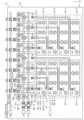
(VCSELアレイ10の等価回路)
図6は、第1の実施の形態が適用される発光装置4におけるVCSELアレイ10の等価回路の一例である。ここでは、VCSELアレイ10の動作を制御する制御部50を合わせて示している。紙面の左方向がy方向である。なお、制御部50は、図2における計測制御部8に設けられている。
VCSELアレイ10は、VCSELを複数備える。一例として、図4(a)と同様に、7個のVCSELにより1個のVCSEL群が構成されている。図6では、4個のVCSEL群(VCSEL群#1~#4)を示している。(Equivalent circuit of VCSEL array 10)
6 is an example of an equivalent circuit of the
The
そして、VCSELアレイ10は、VCSEL群毎に設定サイリスタSを備える。VCSEL群と設定サイリスタSとは直列接続されている。そして、設定サイリスタSについても、VCSEL群の番号である「i」を付すこととする。つまり、VCSEL群#1の備える設定サイリスタSは、設定サイリスタS1である。The
VCSELアレイ10は、さらに複数の転送サイリスタT、複数の結合ダイオードD、複数の電源線抵抗Rg、スタートダイオードSD、電流制限抵抗R1、R2を備える。ここでは、複数の転送サイリスタTをそれぞれ区別する場合、転送サイリスタT1、T2、T3、…のように、VCSEL群の番号である「i」を付して区別する。結合ダイオードD、電源線抵抗Rgも同様である。後述するように、例えば、転送サイリスタT1は、VCSEL群#1に対応するように設けられている。The
図6は、iが1~4に対応する部分を示している。VCSELアレイ10における「i」は、予め定められた数であってよい。例えば128個、512個、1024個などであってよい。転送サイリスタTの数は、VCSEL群の数と同じであればよい。なお、転送サイリスタTの数は、VCSEL群の数を超えてもよいし、少なくてもよい。Figure 6 shows a portion where i corresponds to 1 to 4. "i" in the
転送サイリスタTは、転送サイリスタT1、T2、T3、…の順に-y方向に配列されている。結合ダイオードDは、結合ダイオードD1、D2、D3、…の順に-y方向に配列されている。なお、結合ダイオードD1は、転送サイリスタT1と転送サイリスタT2との間に設けられている。他の結合ダイオードDも同様である。また、電源線抵抗Rgも、電源線抵抗Rg1、Rg2、Rg3、…の順に-y方向に配列されている。The transfer thyristors T are arranged in the -y direction in the order of transfer thyristors T1, T2, T3, .... The coupling diodes D are arranged in the -y direction in the order of coupling diodes D1, D2, D3, .... Note that the coupling diode D1 is provided between the transfer thyristor T1 and the transfer thyristor T2. The same is true for the other coupling diodes D. In addition, the power supply line resistances Rg are also arranged in the -y direction in the order of power supply line resistances Rg1, Rg2, Rg3, ....
VCSEL、結合ダイオードDは、アノードとカソードとを備える2端子素子である。設定サイリスタS、転送サイリスタTは、アノード、カソード、ゲートを備える3端子素子である。なお、転送サイリスタTのゲートをゲートGt、設定サイリスタSのゲートを、ゲートGsとする。なお、それぞれを区別する場合には、前述したと同様に「i」を付す。
ここで、VCSELで構成される部分を発光部12、設定サイリスタS、転送サイリスタT、結合ダイオードD、スタートダイオードSD、電源線抵抗Rg、電流制限抵抗R1、R2で構成される部分を駆動部11とする。 The VCSEL and the coupling diode D are two-terminal elements having an anode and a cathode. The setting thyristor S and the transfer thyristor T are three-terminal elements having an anode, a cathode, and a gate. The gate of the transfer thyristor T is referred to as gate Gt, and the gate of the setting thyristor S is referred to as gate Gs. When distinguishing between them, "i" is added as described above.
Here, the portion composed of the VCSEL is referred to as a
次に、各素子(VCSEL、設定サイリスタS、転送サイリスタTなど)の接続関係を説明する。
前述したように、VCSELijと設定サイリスタSiとは直列接続されている。つまり、設定サイリスタSiは、アノードが基準電位Vsub(接地電位(GND)など)に接続され、カソードがVCSELijのアノードに並列接続されている。
VCSELijのカソードは、VCSELijを発光/非発光の状態に制御する点灯信号φIが供給される点灯信号線76に共通に接続されている。 Next, the connection relationship of each element (VCSEL, setting thyristor S, transfer thyristor T, etc.) will be described.
As described above, the VCSELij and the setting thyristor Si are connected in series. That is, the anode of the setting thyristor Si is connected to the reference potential Vsub (ground potential (GND) or the like), and the cathode is connected in parallel to the anode of the VCSELij.
The cathodes of the VCSELij are commonly connected to a light-
基準電位Vsubは、後述するように、VCSELアレイ10を構成する基板80の裏面に設けられた裏面電極90(後述する図7、図8参照)を介して供給される。The reference potential Vsub is supplied via a back electrode 90 (see Figures 7 and 8 described below) provided on the back surface of the
転送サイリスタTは、アノードが基準電位Vsubに接続されている。奇数番号の転送サイリスタT1、T3、…は、カソードが転送信号線72に接続されている。転送信号線72は、電流制限抵抗R1を介してφ1端子に接続されている。
偶数番号の転送サイリスタT2、T4、…は、カソードが転送信号線73に接続されている。転送信号線73は、電流制限抵抗R2を介してφ2端子に接続されている。 The anode of the transfer thyristor T is connected to the reference potential Vsub. The cathodes of the odd-numbered transfer thyristors T1, T3, . . . are connected to the
The even-numbered transfer thyristors T2, T4, ... have their cathodes connected to a
結合ダイオードDは、互いに直列接続されている。つまり、一つの結合ダイオードDのカソードが-y方向に隣接する結合ダイオードDのアノードに接続されている。スタートダイオードSDは、アノードが転送信号線73に接続され、カソードが結合ダイオードD1のアノードに接続されている。The coupling diodes D are connected in series with each other. That is, the cathode of one coupling diode D is connected to the anode of the coupling diode D adjacent in the -y direction. The anode of the start diode SD is connected to the
そして、スタートダイオードSDのカソードと結合ダイオードD1のアノードとが、転送サイリスタT1のゲートGt1に接続されている。結合ダイオードD1のカソードと結合ダイオードD2のアノードとが、転送サイリスタT2のゲートGt2に接続されている。他の結合ダイオードDについても同様である。The cathode of the start diode SD and the anode of the coupling diode D1 are connected to the gate Gt1 of the transfer thyristor T1. The cathode of the coupling diode D1 and the anode of the coupling diode D2 are connected to the gate Gt2 of the transfer thyristor T2. The same applies to the other coupling diodes D.
転送サイリスタTのゲートGtは、電源線抵抗Rgを介して、電源線71に接続されている。電源線71は、Vgk端子に接続されている。
そして、転送サイリスタTのゲートGtと、設定サイリスタSのゲートGsとは、配線75により接続されている。つまり、転送サイリスタTiのゲートGtiと設定サイリスタSiのゲートGsiとは、配線75-iにより接続されている。配線75を区別する場合には、前述と同様に「i」を付し、配線75-iと表記する場合がある。なお、図6では、iが1~4の部分を示している。配線75は、ゲート信号線の一例である。 The gate Gt of the transfer thyristor T is connected to a
The gate Gt of the transfer thyristor T and the gate Gs of the setting thyristor S are connected by a wiring 75. That is, the gate Gti of the transfer thyristor Ti and the gate Gsi of the setting thyristor Si are connected by a wiring 75-i. When distinguishing the wirings 75, as described above, the letter "i" may be added and they may be written as wirings 75-i. In FIG. 6, i indicates the
制御部50の構成を説明する。
制御部50は、点灯信号φIなどの信号を生成してVCSELアレイ10に供給する。VCSELアレイ10は、供給された信号によって動作する。制御部50は、電子回路で構成されている。例えば、制御部50は、VCSELアレイ10の動作を制御するために構成された集積回路(IC)であってもよい。
制御部50は、転送信号生成部51、点灯信号生成部52、電源電位生成部53及び基準電位生成部54を備える。 The configuration of the
The
The
転送信号生成部51は、転送信号φ1、φ2を生成し、転送信号φ1をVCSELアレイ10のφ1端子に、転送信号φ2をVCSELアレイ10のφ2端子に供給する。
点灯信号生成部52は、点灯信号φIを生成し、電流制限抵抗RIを介して、VCSELアレイ10のφI端子に供給する。なお、電流制限抵抗RIは、VCSELアレイ10内に設けられてもよい。また、電流制限抵抗RIがVCSELアレイ10の動作に必要でない場合には、電流制限抵抗RIを設けなくともよい。 The transfer
The light-up
電源電位生成部53は、電源電位Vgkを生成し、VCSELアレイ10のVgk端子に供給する。基準電位生成部54は、基準電位Vsubを生成し、VCSELアレイ10のVsub端子に供給する。電源電位Vgkは、一例として-3.3Vである。基準電位Vsubは、前述したように、一例として接地電位(GND)である。The power supply
転送信号生成部51の生成する転送信号φ1、φ2、点灯信号生成部52が生成する点灯信号φIについては、後述する。The transfer signals φ1 and φ2 generated by the transfer
図6に示したVCSELアレイ10では、1個の転送サイリスタTiには、7個のVCSELij(j=1~7)がVCSEL群として、設定サイリスタSiを介して接続されている。
後述するように、転送サイリスタTiは、オン状態になることで、転送サイリスタTiに接続された設定サイリスタSiをオン状態に移行可能に設定する。よって、VCSELを発光可能な状態に設定することから設定サイリスタSと表記する。また、設定サイリスタSiがオン状態なると、VCSELijが発光する。なお、転送サイリスタTiは、「i」の順にオン状態を転送するように駆動される。つまり、転送サイリスタTiにおいて、オン状態が順に伝搬する。これにより、転送サイリスタTiは、VCSEL群を順次点灯(発光)させている。
ここでは、複数のVCSELにより1個のVCSEL群が構成されている。そして、転送サイリスタT毎に、VCSEL群が接続され、VCSEL群に含まれる複数のVCSELが並行して発光する。 In the
As will be described later, when the transfer thyristor Ti is turned on, it sets the setting thyristor Si connected to the transfer thyristor Ti to be able to transition to the on state. Therefore, since the VCSEL is set to a state in which it can emit light, it is represented as the setting thyristor S. Also, when the setting thyristor Si is turned on, the VCSELij emits light. Note that the transfer thyristors Ti are driven to transfer the on state in the order of "i". In other words, the on state propagates in sequence in the transfer thyristor Ti. As a result, the transfer thyristor Ti sequentially lights up (emits light) the VCSEL group.
Here, one VCSEL group is configured by a plurality of VCSELs. The VCSEL group is connected to each transfer thyristor T, and the plurality of VCSELs included in the VCSEL group emit light in parallel.
なお、図6に示す例では、各VCSEL群は、同じ数(ここでは、7個)のVCSELを備えるが、VCSEL群間でVCSELの数が異なってもよい。In the example shown in FIG. 6, each VCSEL group has the same number of VCSELs (here, seven), but the number of VCSELs may differ between the VCSEL groups.
VCSELは、低次の単一横モード(シングルモード)で発振することがよい。シングルモードでは、VCSELの発光点(後述する図8の光出射口310)から出射する光(出射光)の強度プロファイルが単峰性(強度ピークが1つである特性)となる。一方、高次を含む多重横モード(マルチモード)で発振するVCSELでは、複数峰になるなど、強度プロファイルがいびつになりやすい。また、シングルモードでは、マルチモードに比べて、発光点から出射する光(出射光)の拡がり角が小さい。It is preferable for a VCSEL to oscillate in a low-order single transverse mode (single mode). In single mode, the intensity profile of the light (emitted light) emitted from the light-emitting point of the VCSEL (
そして、VCSELは、発光点の面積が小さいほど単一横モード(シングルモード)で発振しやすい。このため、シングルモードのVCSELは、光出力が小さい。光出力を大きくしようとして、発光点の面積を大きくすると、マルチモードに移行しやすい。そこで、複数のVCSELをVCSEL群とし、VCSEL群に含まれる複数のVCSELを並行して発光させることで、光出力を大きくしている。The smaller the area of the light-emitting point of a VCSEL, the more likely it is to oscillate in a single transverse mode (single mode). For this reason, single-mode VCSELs have a small optical output. If the area of the light-emitting point is increased in an attempt to increase the optical output, it is likely to transition to multimode. For this reason, multiple VCSELs are grouped into a VCSEL group, and the multiple VCSELs in the VCSEL group are made to emit light in parallel, thereby increasing the optical output.
(VCSELアレイ10の平面レイアウト)
図7は、第1の実施の形態が適用されるVCSELアレイ10の平面レイアウトの一例を示す図である。図7において、紙面の上方向がx方向、左方向がy方向である。
VCSELアレイ10は、レーザ光を出射しうる半導体材料で構成される。例えば、VCSELアレイ10は、GaAs系の化合物半導体で構成される。そして、後述する断面図(後述する図8)に示すように、VCSELアレイ10は、p型のGaAsの基板80上に、GaAs系の化合物半導体層が複数積層された半導体層積層体が複数の島状に分離されることで構成される。なお、島状に残された領域は、アイランドと呼ばれる。半導体層積層体を島状にエッチングして、素子を分離することは、メサエッチングと呼ばれる。ここでは、図7に示すアイランド301~306により、VCSELアレイ10の平面レイアウトを説明する。なお、アイランド301、302、303は、VCSEL群毎に設けられる。よって、アイランド301、302、303を、VCSEL群ごとに区別する場合には、前述と同様に「i」を付し、アイランド301-i、302-i、303-iと表記する場合がある。なお、図7では、iが1~8の部分を示している。また、VCSEL群におけるVCSELの数を前述と同様に「j」と表記する。ここでは、jは1~7である。このように、VCSELアレイ10は、共通の半導体基板に構成されている。よって、発光装置4が小型化される。(Plane layout of the VCSEL array 10)
7 is a diagram showing an example of a planar layout of the
The
アイランド301-iには、VCSELij、設定サイリスタSiが設けられている。なお、後述する図8に示すように、VCSELijと設定サイリスタSiとは、積層されている。なお、図7では、VCSELijと設定サイリスタSiとを、VCSELij/Siと表記する。例えば、「i」が1の場合、VCSEL1j/S1と表記する。iが1~4のアイランド301-iと、iが5~8のアイランド301-iとは、-x方向に並列に配列されている。そして、iが1~4のアイランド301-iと、iが5~8のアイランド301-iとは、-y方向に並列に配列されている。Island 301-i is provided with VCSELij and a setting thyristor Si. As shown in FIG. 8, which will be described later, VCSELij and the setting thyristor Si are stacked. In FIG. 7, VCSELij and the setting thyristor Si are expressed as VCSELij/Si. For example, when "i" is 1, it is expressed as VCSEL1j/S1. Islands 301-i with i of 1 to 4 and islands 301-i with i of 5 to 8 are arranged in parallel in the -x direction. Islands 301-i with i of 1 to 4 and islands 301-i with i of 5 to 8 are arranged in parallel in the -y direction.
なお、アイランド301-iにおいて、図4(a)におけるVCSEL群#1に示したように、7個のVCSELが配列されている。なお、符号は付さない。In addition, seven VCSELs are arranged in island 301-i, as shown in
アイランド302-iには、転送サイリスタTi及び結合ダイオードDiが設けられている。アイランド302-iは、-y方向に並列するように設けられている。A transfer thyristor Ti and a coupling diode Di are provided in the island 302-i. The islands 302-i are arranged in parallel in the -y direction.
アイランド303-iには、電源線抵抗Rgiが設けられている。アイランド303-iは、-y方向に並列するように設けられている。A power supply line resistance Rgi is provided on island 303-i. Island 303-i is arranged in parallel in the -y direction.
アイランド304には、スタートダイオードSDが設けられている。アイランド305には、電流制限抵抗R1が、アイランド306には、電流制限抵抗R2が設けられている。A start diode SD is provided on
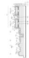
(VCSELアレイ10の断面構造)
次に、これらのアイランド301~306の接続関係を説明する前に、アイランド301、302の断面構造を説明する。(Cross-sectional structure of the VCSEL array 10)
Next, before describing the connection relationship of these
図8は、VCSELアレイ10の断面構造を示す図である。なお、図8は、図7におけるVIII-VIII線でのVCSELアレイ10の断面図である。つまり、図8に示す断面図は、紙面において、左側から結合ダイオードD1、転送サイリスタT1、VCSEL11/S1、VCSEL12/S1を横切る断面である。つまり、アイランド301-1とアイランド302-1の部分を示している。Figure 8 is a diagram showing the cross-sectional structure of the
まず、設定サイリスタSとVCSELとが設けられたアイランド301-1を説明する。ここでは、設定サイリスタSとVCSELとが積層されて構成されている(VCSEL11/S1、VCSEL12/S1)。図8に示すように、p型のGaAsの基板80上に、設定サイリスタS1を構成するp型のアノード層(以下では、pアノード層と表記する。以下同様とする。)81、n型のゲート層(nゲート層)82、p型のゲート層(pゲート層)83、n型のカソード層(nカソード層)84が積層されている。つまり、設定サイリスタSは、pアノード層81をアノード、nゲート層82をnゲート、pゲート層83をpゲート、nカソード層84をカソードとして構成されている。First, the island 301-1 in which the setting thyristor S and the VCSEL are provided will be described. Here, the setting thyristor S and the VCSEL are stacked (VCSEL11/S1, VCSEL12/S1). As shown in FIG. 8, a p-type anode layer (hereinafter referred to as p-anode layer, and the same applies below) 81, an n-type gate layer (n-gate layer) 82, a p-type gate layer (p-gate layer) 83, and an n-type cathode layer (n-cathode layer) 84 constituting the setting thyristor S1 are stacked on a p-
次に、nカソード層84上にトンネル接合層85が積層されている。
そして、トンネル接合層85上に、VCSEL11、VCSEL12を構成するp型のアノード層(pアノード層)86、発光層87、n型のカソード層(nカソード層)88が積層されている。つまり、VCSELは、pアノード層86をアノード、発光層87を発光層、nカソード層88をカソードとして構成されている。
設定サイリスタS1とVCSEL11、VCSEL12とは、トンネル接合層85を介して直列接続されている。トンネル接合層85については後述する。 Next, a
A p-type anode layer (p anode layer) 86, a
The setting thyristor S1, the VCSEL11, and the VCSEL12 are connected in series via a
VCSEL11及びVCSEL12の部分では、VCSELの周囲のトンネル接合層85が露出するように、nカソード層88、発光層87、pアノード層86がエッチングにより除去されている。ここでは、VCSELの断面形状が円形になっている。つまり、VCSELの部分は、円柱状に形成されている。よって、VCSELの部分をポスト311と表記する(図7参照)。In the VCSEL11 and VCSEL12 portions, the n-
設定サイリスタSを構成するpアノード層81、nゲート層82、pゲート層83、nカソード層84、トンネル接合層85は、VCSEL群#1に属するVCSEL(VCSEL11~17)間で連続する。The p-
また、アイランド301-1では、さらにトンネル接合層85とnカソード層84とを除去してpゲート層83を露出させた部分に、pゲート層83などp型の半導体層とオーミック接触が形成しやすい金属材料で構成されたpオーミック電極331が、設定サイリスタS1のゲートGs1として設けられている。In addition, in the island 301-1, the
VCSELのnカソード層88上には、nカソード層88などn型の半導体層とオーミック接触が形成しやすい金属材料で構成されたnオーミック電極321が設けられている。なお、nオーミック電極321は、光出射口310を取り囲むように、円形に設けられている(図7参照)。On the n-
ポスト311のpアノード層86には、電流狭窄層86bが含まれる。ここでは、一例として、pアノード層86は、下側pアノード層86a、電流狭窄層86b、上側pアノード層86cの3層から構成されている。電流狭窄層86bは、AlAsのように、Alの組成比が高い材料で構成され、酸化によりAlがAl2O3になることにより、電気抵抗が高くなって、電流が流れにくくなる部分(図8中の黒塗りの部分)が形成される層をいう。 The
ポスト311は円柱状に設けられているので、露出したpアノード層86の側面から電流狭窄層86bの酸化を行うと、円形の断面における周辺部から中心部へと酸化が進む。そして、中心部を酸化させないことで、VCSELの断面における中心部が電流の流れやすい電流通過領域86dとなり、周辺部が電流の流れにくい電流阻止領域86eとなる。なお、VCSELは、発光層87の電流通過領域86dにより電流経路が制限された部分において発光が生じる。この電流通過領域86dに対応するVCSELの表面の領域が発光点であり、光出射口310である。Since the
電流狭窄層86bを設けるのは、VCSELを低次の単一横モード(シングルモード)で発振させるためである。つまり、VCSELが形成されるポスト311の断面形状を円形にして周辺部から酸化させることで、光出射口310の断面形状を円形とするとともに、面積を小さくしている。
また、VCSELの周辺部は、メサエッチングに起因した欠陥が多く、非発光再結合が起こりやすい。このため、電流阻止領域86eを設けることで、非発光再結合に消費される電力が抑制される。よって、低消費電力化及び光取り出し効率の向上が図れる。なお、光取り出し効率とは、電力当たりに取り出すことができる光量である。 The
In addition, the peripheral portion of the VCSEL has many defects due to mesa etching, and non-radiative recombination is likely to occur. Therefore, by providing the
次に、転送サイリスタT1と結合ダイオードD1とが設けられたアイランド302-1を説明する。転送サイリスタT1は、設定サイリスタSと同様に、pアノード層81、nゲート層82、pゲート層83、nカソード層84で構成される。つまり、転送サイリスタT1は、pアノード層81をアノード、nゲート層82をnゲート、pゲート層83をpゲート、nカソード層84をカソードとして構成される。ここでは、pゲート層83上にゲート電極(後述するpオーミック電極332)が設けられている。Next, the island 302-1 in which the transfer thyristor T1 and the coupling diode D1 are provided will be described. The transfer thyristor T1 is composed of a p-
結合ダイオードD1は、pゲート層83、nカソード層84で構成されている。つまり、結合ダイオードD1は、pゲート層83をアノード、nカソード層84をカソードとして構成されている。The coupling diode D1 is composed of a
アイランド302-1では、設定サイリスタSとVCSELとが積層された部分におけるnカソード層88、発光層87、pアノード層86及びトンネル接合層85が除去されている。そして、転送サイリスタT1の部分と、結合ダイオードD1の部分とにおいて、nカソード層84がポスト312と、ポスト313として残るように、nカソード層84が除去されている。In island 302-1, the n-
ポスト312のnカソード層84上に、nオーミック電極322が転送サイリスタT1のカソード電極として設けられている。同様に、ポスト313のnカソード層84上に、nオーミック電極323が結合ダイオードD1のカソード電極として設けられている。An n-
pゲート層83上に設けられたpオーミック電極332は、転送サイリスタT1のゲートGt1及び結合ダイオードD1のアノード電極として機能する。The p-
そして、表面を覆うように層間絶縁層91が設けられている。層間絶縁層91上には、スルーホール(開口)を介して、アイランド301-1に設けられたpオーミック電極331(ゲートGs1)とアイランド302-1に設けられたpオーミック電極332(ゲートGt1)とを接続する配線75-1と、アイランド301-2に設けられたpオーミック電極(ゲートGs2)とアイランド302-2に設けられたpオーミック電極(ゲートGt1)とを接続する配線75-2が設けられている。また、層間絶縁層91上には、nオーミック電極322に接続された転送信号線72が設けられている。そして、層間絶縁層91上には、転送信号線73が設けられている。さらに、層間絶縁層91上には、スルーホールを介して、nオーミック電極323に接続された配線74-2が設けられている。An interlayer insulating
さらに、表面を覆うように層間絶縁層92が設けられている。そして、層間絶縁層92上には、層間絶縁層92及び層間絶縁層91に設けたスルーホールを介して、アイランド301-1に設けられたnオーミック電極321に接続された点灯信号線76が設けられている。つまり、配線75(配線75-1、75-2)と点灯信号線76とは、層間絶縁層92を介した多層配線構造となっている。Furthermore, an
なお、層間絶縁層91、92が、VCSELの出射光に対して透過性が劣る場合には、光出射口310上の層間絶縁層91、92の代わりに、VCSELの出射光に対して透過性に優れる光出射層を設けてもよい。In addition, if the
アイランド301、302、303、304、305、306は、周囲の半導体層積層体が基板80に至るまでエッチングにより除去されることで、互いに分離されている。なお、pアノード層81に至るまでエッチングされてもよく、pアノード層81の厚さ方向の一部に至るまでエッチングされてもよい。The
図7に戻って、他のアイランド303、304、305、306を説明する。アイランド303には、電源線抵抗Rg1が構成されている。アイランド303-1は、半導体層積層体におけるnカソード層88、発光層87、pアノード層86、トンネル接合層85、nカソード層84が除去されて、pゲート層83を露出させている。露出させたpゲート層83上に一対のpオーミック電極が設けられている。そして、pオーミック電極間のpゲート層83が抵抗として用いられている。Returning to FIG. 7, the
アイランド304には、スタートダイオードSDが設けられている。アイランド304は、半導体層積層体におけるnカソード層88、発光層87、pアノード層86、トンネル接合層85が除去されている。そして、nカソード層84が残されたポスト314を除いて、pゲート層83を露出させている。スタートダイオードSDは、ポスト314を構成するnカソード層84がカソード、pゲート層83がアノードである。そして、ポスト314のnカソード層84上に設けられたnオーミック電極がカソード電極、露出させたpゲート層83上に設けられたpオーミック電極がアノード電極である。The start diode SD is provided on the
アイランド305には、電流制限抵抗R1、アイランド306には、電流制限抵抗R2が設けられている。アイランド305、306は、アイランド303と同様の構成であって、露出させたpゲート層83上に設けられた1対のpオーミック電極間のpゲート層83をそれぞれ電流制限抵抗R1、R2とする。
アイランド301~306及びアイランド間の接続関係を説明する。
前述したように、アイランド301-1のポスト311に設けられたVCSELのカソードであるnカソード層88は、nオーミック電極321を介して、点灯信号線76に並列に接続される。他のアイランド301も同様である。
アイランド302-1のポスト312に設けられた転送サイリスタT1のカソードであるnカソード層88は、nオーミック電極322を介して、転送信号線72に接続されている。なお、アイランド302-3(-y方向側の3番目に位置するアイランド302)に設けられた転送サイリスタT3も同様である。つまり、奇数番号iの転送サイリスタTiのカソード(nカソード層88)は、転送信号線72に接続されている。 The
As described above, the n-
The n-
一方、アイランド302-2(-y方向側の2番目に位置するアイランド302)に設けられた転送サイリスタT2のカソード(nカソード層88)は、転送信号線73に接続されている。つまり、偶数番号iの転送サイリスタTiのカソード(nカソード層88)は、転送信号線73に接続されている。On the other hand, the cathode (n-cathode layer 88) of the transfer thyristor T2 provided in the island 302-2 (the
そして、アイランド301-1のゲートGs1であるpオーミック電極331とアイランド301-2のゲートGt1であるpオーミック電極332とは、配線75-1で接続されている。アイランド302-1のポスト313に設けられた結合ダイオードD1のカソード(nカソード層88)は、nオーミック電極323(図8参照)を介して、配線74-2に接続されている。配線74-2は、隣接するアイランド302-2のpオーミック電極(符号なし)及びアイランド303-2の電源線抵抗Rg2のpオーミック電極(符号なし)に接続されている。The p-
アイランド302-1に設けられたpオーミック電極333(ゲートGt1のpオーミック電極332と同様にpゲート層83上に設けられている。)と、アイランド303-1に設けられた電源線抵抗Rg1の一方のpオーミック電極と、アイランド304に設けられたスタートダイオードSDのカソード電極であるnオーミック電極とは、配線74-1により接続されている。The p-ohmic electrode 333 (provided on the
また、アイランド303-1の電源線抵抗Rg1の他方のpオーミック電極は、電源線71に接続されている。電源線71は、Vgk端子に接続されている。他のアイランド303も同様である。The other p-ohmic electrode of the power supply line resistor Rg1 of island 303-1 is connected to the
転送信号線72は、アイランド305の電流制限抵抗R1の一方のpオーミック電極(符号なし)に接続されている。電流制限抵抗R1の他方のpオーミック電極(符号なし)は、φ1端子に接続されている。転送信号線73は、アイランド303のスタートダイオードSDのpオーミック電極に接続されるとともに、アイランド306の電流制限抵抗R2の一方のpオーミック電極(符号なし)に接続されている。アイランド306の電流制限抵抗R2の他方のpオーミック電極(符号なし)は、φ2端子に接続されている。The
以上においては、アイランド301-1、302-1、303-1を例として説明したが、他のアイランド301、302、303でも同様である。よって、図7では、例えば、配線74-1(74)などのように表記して、他の配線74も同様であることを示す。The above has been described using islands 301-1, 302-1, and 303-1 as examples, but the same applies to the
<サイリスタ>
次に、設定サイリスタS、転送サイリスタTの動作について説明する。設定サイリスタSと転送サイリスタTとをまとめてサイリスタと表記する。
サイリスタは、pアノード層81、nゲート層82、pゲート層83、nカソード層84が積層されて構成されている。
サイリスタは、前述したように、アノード、カソード、ゲートの3端子を有する半導体素子であって、例えば、GaAs、GaAlAs、AlAsなどによるp型の半導体層(pアノード層81、pゲート層83)、n型の半導体層(nゲート層82、nカソード層84)を積層して構成されている。つまり、サイリスタは、pnpn構造を成している。ここでは、一例として、p型の半導体層とn型の半導体層とで構成されるpn接合の順方向電位(拡散電位)Vdを1.5Vとする。<Thyristor>
Next, there will be described the operations of the setting thyristor S and the transfer thyristor T. The setting thyristor S and the transfer thyristor T are collectively referred to as thyristors.
The thyristor is configured by laminating a p-
As described above, a thyristor is a semiconductor element having three terminals, an anode, a cathode, and a gate, and is configured by stacking a p-type semiconductor layer (
一例として、pアノード層81の基準電位Vsubをハイレベルの電位(以下では「H」と表記する。)として0V、Vgk端子(図6参照)に供給される電源電位Vgkをローレベルの電位(以下では「L」と表記する。)として-3.3Vとする。よって、「H(0V)」、「L(-3.3V)」と表記することがある。図6に示したように、Vgk端子は、電源線抵抗Rgを介して、ゲートに接続されている。つまり、サイリスタが転送サイリスタT1の場合、Vgk端子は、電源線抵抗Rg1を介して、ゲートGt1に接続されている。As an example, the reference potential Vsub of the
アノードとカソードとの間に電流が流れていないオフ状態のサイリスタは、しきい電圧より低い電位(絶対値が大きい負の電位)がカソードに印加されるとオン状態に移行(ターンオン)する。ここで、サイリスタのしきい電圧は、ゲートの電位からpn接合の順方向電位Vd(1.5V)を引いた値である。
オン状態になると、サイリスタのゲートは、アノードの電位に近い電位になる。ここでは、アノードは0Vであるので、ゲートは0Vになるとする。また、オン状態のサイリスタのカソードは、アノードの電位からpn接合の順方向電位Vd(1.5V)を引いた電位に近い電位(絶対値を保持電圧と表記する。)となる。ここでは、アノードは0Vであるので、オン状態のサイリスタのカソードは、-1.5Vに近い電位(絶対値が1.5Vより大きい負の電位)となる。ここでは、保持電圧は、1.5Vであるとする。 A thyristor in the off state, where no current flows between the anode and cathode, transitions to the on state (turns on) when a potential lower than the threshold voltage (a negative potential with a large absolute value) is applied to the cathode. Here, the threshold voltage of a thyristor is the value obtained by subtracting the forward potential Vd (1.5 V) of the pn junction from the gate potential.
When the thyristor is turned on, the gate of the thyristor has a potential close to that of the anode. In this case, the anode is 0V, so the gate is assumed to be at 0V. Also, the cathode of the thyristor in the on state has a potential close to the potential of the anode minus the forward potential Vd (1.5V) of the pn junction (the absolute value of which is denoted as the holding voltage). In this case, the anode is 0V, so the cathode of the thyristor in the on state has a potential close to -1.5V (a negative potential with an absolute value greater than 1.5V). In this case, the holding voltage is assumed to be 1.5V.
オン状態のサイリスタは、カソードにオン状態を維持するために必要な電位より低い電位(絶対値が大きい負の電位)が継続的に印加され、オン状態を維持しうる電流(維持電流)が供給されると、オン状態を維持する。
一方、オン状態のサイリスタは、カソードがオン状態を維持するために必要な電位(上記の-1.5Vに近い電位)より高い電位(絶対値が小さい負の電位、0V又は正の電位)になると、オフ状態に移行(ターンオフ)する。 A thyristor in the on state maintains its on state when a potential lower than the potential required to maintain the on state (a negative potential with a large absolute value) is continuously applied to the cathode and a current sufficient to maintain the on state (maintenance current) is supplied.
On the other hand, a thyristor in the on state transitions to the off state (turns off) when the cathode reaches a potential (a negative potential with a small absolute value, 0 V, or a positive potential) higher than the potential required to maintain the on state (a potential close to the above-mentioned -1.5 V).
<トンネル接合層85>
次に、図8に示したように、アイランド301における設定サイリスタSとVCSELとは、トンネル接合層85を介して積層されている。これにより、設定サイリスタSとVCSELとが、直列接続されている。
図9は、設定サイリスタSとVCSELとの積層構造をさらに説明する図である。図9(a)は、設定サイリスタSとVCSELとの積層構造における模式的なエネルギーバンド図、図9(b)は、トンネル接合層85の逆バイアス状態におけるエネルギーバンド図、図9(c)は、トンネル接合層85の電流電圧特性を示す。<
8, the setting thyristor S and the VCSEL in the
9A and 9B are diagrams further explaining the stacked structure of the setting thyristor S and the VCSEL. Fig. 9A is a schematic energy band diagram of the stacked structure of the setting thyristor S and the VCSEL, Fig. 9B is an energy band diagram of the
図7、図8に示したnオーミック電極321に印加される点灯信号φIと裏面電極90の基準電位Vsubとの間に、設定サイリスタSとVCSELとのそれぞれが順バイアスになるように電圧を印加する。すると、図9(a)のエネルギーバンド図に示すように、トンネル接合層85を構成するn++層85aとp++層85bとの間が逆バイアスになる。 7 and 8, a voltage is applied between the light-up signal φI applied to the n-
トンネル接合層85は、n型の不純物を高濃度に添加したn++層85aと、p型の不純物を高濃度に添加したp++層85bとの接合である。このため、空乏領域の幅が狭く、順バイアスされると、n++層85a側の伝導帯(コンダクションバンド)からp++層85b側の価電子帯(バレンスバンド)に電子がトンネルする。この際、負性抵抗特性が表れる(図9(c)の順バイアス側(+V)参照)。 The
一方、図9(b)に示すように、トンネル接合層85は、逆バイアス(-V)されると、p++層85b側の価電子帯(バレンスバンド)の電位Evが、n++層85a側の伝導帯(コンダクションバンド)の電位Ecより上になる。そして、p++層85bの価電子帯(バレンスバンド)から、n++層85a側の伝導帯(コンダクションバンド)に電子がトンネルする。そして、逆バイアス電圧(-V)が大きくなるほど、電子のトンネルがしやすくなる。すなわち、図9(c)の逆バイアス側(-V)に示すように、トンネル接合層85(トンネル接合)は、逆バイアスが大きいほど、電流が流れやすい。 On the other hand, as shown in FIG. 9(b), when the
よって、図9(a)に示すように、設定サイリスタSとVCSELとのそれぞれが順バイアスになるように電圧が印加され、設定サイリスタSがターンオンしてオン状態に移行すると、トンネル接合層85が逆バイアスであっても、設定サイリスタSからVCSELへ電流が流れる。Therefore, as shown in FIG. 9(a), when a voltage is applied to the setting thyristor S and the VCSEL so that they are both forward biased, and the setting thyristor S is turned on and transitions to the on state, a current flows from the setting thyristor S to the VCSEL even if the
なお、トンネル接合層85の代わりに、金属的な導電性を有し、III-V族の化合物半導体層にエピタキシャル成長するIII-V族化合物層を用いてもよい。金属的導電性III-V族化合物層の材料の一例として説明するInNAsは、例えばInNの組成比xが約0.1~約0.8の範囲において、バンドギャップエネルギが負になる。また、InNSbは、例えばInNの組成比xが約0.2~約0.75の範囲において、バンドギャップエネルギが負になる。バンドギャップエネルギが負になることは、バンドギャップを持たないことを意味する。よって、金属と同様な導電特性(伝導特性)を示すことになる。すなわち、金属的な導電特性(導電性)とは、金属と同様に電位に勾配があれば電流が流れることをいう。In place of the
そして、GaAs、InPなどのIII-V族化合物(半導体)の格子定数は、5.6Å~5.9Åの範囲にある。そして、この格子定数は、Siの格子定数の約5.43Å、Geの格子定数の約5.66Åに近い。
これに対して、同様にIII-V族化合物であるInNの格子定数は、閃亜鉛鉱構造において約5.0Å、InAsの格子定数は、約6.06Åである。よって、InNとInAsとの化合物であるInNAsの格子定数は、GaAsなどの5.6Å~5.9Åに近い値になりうる。
また、III-V族化合物であるInSbの格子定数は、約6.48Åである。よって、InNの格子定数の約5.0Åであるので、InSbとInNとの化合物であるInNSbの格子定数は、GaAsなど5.6Å~5.9Åに近い値になりうる。 The lattice constant of III-V group compounds (semiconductors) such as GaAs and InP is in the range of 5.6 Å to 5.9 Å, which is close to the lattice constant of Si, which is about 5.43 Å, and the lattice constant of Ge, which is about 5.66 Å.
In contrast, the lattice constant of InN, which is also a III-V compound, is about 5.0 Å in a zinc blende structure, and the lattice constant of InAs is about 6.06 Å. Therefore, the lattice constant of InNAs, which is a compound of InN and InAs, can be close to the 5.6 Å to 5.9 Å of GaAs and the like.
The lattice constant of InSb, a III-V compound, is about 6.48 Å. Since the lattice constant of InN is about 5.0 Å, the lattice constant of InNSb, a compound of InSb and InN, can be close to the lattice constant of GaAs, which is 5.6 Å to 5.9 Å.
すなわち、InNAs及びInNSbは、GaAsなどのIII-V族化合物(半導体)の層に対してモノリシックにエピタキシャル成長させうる。また、InNAs又はInNSbの層上に、GaAsなどのIII-V族化合物(半導体)の層をエピタキシャル成長によりモノリシックに積層させうる。That is, InNAs and InNSb can be monolithically epitaxially grown on a layer of a III-V compound (semiconductor) such as GaAs. Also, a layer of a III-V compound (semiconductor) such as GaAs can be monolithically stacked by epitaxial growth on a layer of InNAs or InNSb.
よって、トンネル接合層85の代わりに、金属的導電性III-V族化合物層を介して、設定サイリスタSとVCSELとを直列接続されるように積層すれば、設定サイリスタSのnカソード層84とVCSELのpアノード層86とが逆バイアスになることが抑制される。Therefore, if the setting thyristor S and the VCSEL are stacked so as to be connected in series via a metallic conductive III-V compound layer instead of the
<積層された設定サイリスタSとVCSELの動作>
次に、積層された設定サイリスタSとVCSELの動作を説明する。
ここで、VCSELは、立ち上がり電圧を1.5Vとする。つまり、VCSELのアノードとカソードとの間に1.5V以上の電圧が印加されていれば、VCSELが発光する。
点灯信号φIは、0V(「H(0V)」)又は-3.3V(「L(-3.3V)」)であるとする。0Vは、VCSELをオフ状態にする電位、-3.3Vは、VCSELをオフ状態からオン状態にする電位である。<Operation of stacked setting thyristors S and VCSELs>
Next, the operation of the stacked setting thyristor S and VCSEL will be described.
Here, the VCSEL has a turn-on voltage of 1.5 V. In other words, if a voltage of 1.5 V or more is applied between the anode and cathode of the VCSEL, the VCSEL emits light.
The light-up signal φI is assumed to be 0 V ("H (0 V)") or -3.3 V ("L (-3.3 V)"), where 0 V is a potential that turns the VCSEL off, and -3.3 V is a potential that turns the VCSEL from an off state to an on state.
VCSELをオフ状態からオン状態に移行させる場合、点灯信号φIが、「L(-3.3V)」に設定される。このとき、設定サイリスタSのゲートGsに-1.5Vが印加されると、設定サイリスタSのしきい値は、ゲートGsの電位(-1.5V)からpn接合の順方向電位Vd(1.5V)を引いた、-3Vになる。このとき、点灯信号φIは、-3.3Vであるので、設定サイリスタSがターンオンしてオフ状態からオン状態に移行するとともに、VCSELもオフ状態からオン状態に移行する。つまり、VCSELは、レーザ発振して発光する。すると、オン状態の設定サイリスタSに印加される電圧(保持電圧Vr)は1.5Vであるので、レーザダイオードLDには1.8Vが印加される。なお、VCSELは立ち上がり電圧が1.5Vであるので、VCSELは、発光を継続する。When the VCSEL is changed from the OFF state to the ON state, the lighting signal φI is set to "L (-3.3V)". At this time, when -1.5V is applied to the gate Gs of the setting thyristor S, the threshold of the setting thyristor S becomes -3V, which is the potential of the gate Gs (-1.5V) minus the forward potential Vd (1.5V) of the pn junction. At this time, since the lighting signal φI is -3.3V, the setting thyristor S turns on and changes from the OFF state to the ON state, and the VCSEL also changes from the OFF state to the ON state. In other words, the VCSEL emits light by laser oscillation. Then, since the voltage (holding voltage Vr) applied to the setting thyristor S in the ON state is 1.5V, 1.8V is applied to the laser diode LD. Note that the VCSEL continues to emit light because the rise voltage is 1.5V.
一方、点灯信号φIを0Vにすると、設定サイリスタSとVCSELとの直列接続の両端が0Vになり、設定サイリスタSがオン状態からオフ状態に移行(ターンオフ)するとともに、VCSELが非発光になる。
VCSELアレイ10の動作については、後に詳述する。 On the other hand, when the light-up signal φI is set to 0 V, both ends of the series connection of the setting thyristor S and the VCSEL become 0 V, the setting thyristor S transitions from the on state to the off state (turns off), and the VCSEL stops emitting light.
The operation of the
(半導体層積層体の構成)
半導体層積層体は、前述したように、基板80、pアノード層81、nゲート層82、pゲート層83、nカソード層84、トンネル接合層85、pアノード層86、発光層87、nカソード層88が積層されて構成されている。
上述したように、基板80は、p型のGaAsを例として説明するが、n型のGaAs、不純物を添加していないイントリンシック(i)のGaAsでもよい。また、InP、GaN、InAs、その他III-V族、II-VI材料からなる半導体基板、サファイア、Si、Geなどでもよい。基板を変更した場合、基板上にモノリシックに積層される材料は、基板の格子定数に略整合(歪構造、歪緩和層、メタモルフィック成長を含む)する材料を用いる。一例として、InAs基板上には、InAs、InAsSb、GaInAsSbなどを使用し、InP基板上にはInP、InGaAsPなどを使用し、GaN基板上又はサファイア基板上には、GaN、AlGaN、InGaNを使用し、Si基板上にはSi、SiGe、GaPなどを使用する。ただし、基板80が電気絶縁性である場合には、基準電位Vsubを供給する配線を別途設けることが必要となる。また、基板80を除く半導体層積層体を他の支持基板に張り付け、他の支持基板上に半導体層積層体を設ける場合は、支持基板と格子定数が整合している必要はない。(Configuration of Semiconductor Layer Stack)
As described above, the semiconductor layer stack is composed of a
As described above, the
pアノード層81は、例えば不純物濃度1×10¹⁸/cm3のp型のAl0.9GaAsである。Al組成は、0~1の範囲で変更してもよい。
nゲート層82は、例えば不純物濃度1×10¹⁷/cm3のn型のAl0.9GaAsである。Al組成は、0~1の範囲で変更してもよい。
pゲート層83は、例えば不純物濃度1×10¹⁷/cm3のp型のAl0.9GaAsである。Al組成は、0~1の範囲で変更してもよい。
nカソード層84は、例えば不純物濃度1×10¹⁸/cm3のn型のAl0.9GaAsである。Al組成は、0~1の範囲で変更してもよい。 The p-
The
The
The n-
トンネル接合層85は、n型の不純物を高濃度に添加したn++層85aとn型の不純物を高濃度に添加したp++層85bとの接合(図7(a)参照。)で構成されている。n++層85a及びp++層85bは、例えば不純物濃度1×10²⁰/cm3と高濃度である。なお、通常の接合の不純物濃度は、1017/cm3台~1018/cm3台である。n++層85aとp++層85bとの組み合わせ(以下では、n++層85a/p++層85bで表記する。)は、例えばn++GaInP/p++GaAs、n++GaInP/p++AlGaAs、n++GaAs/p++GaAs、n++AlGaAs/p++AlGaAs、n++InGaAs/p++InGaAs、n++GaInAsP/p++GaInAsP、n++GaAsSb/p++GaAsSbである。なお、組み合わせを相互に変更したものでもよい。 The
pアノード層86は、下側pアノード層86a、電流狭窄層86b、上側pアノード層86cを順に積層して構成されている。下側pアノード層86a、上側pアノード層86cは、例えば不純物濃度5×10¹⁷/cm3のp型のAl0.9GaAsである。Al組成は、0~1の範囲で変更してもよい。
電流狭窄層86bは、例えばAlAs又はAlの不純物濃度が高いp型のAlGaAsである。Alが酸化されてAl2O3が形成されることにより、電気抵抗が高くなって、電流阻止領域86eが形成されるものであればよい。なお、GaAs、AlGaAsなどの半導体層に水素イオン(H+)を打ち込むことで、電流阻止領域86eを形成してもよい(H+イオン打ち込み)。 The
The
発光層87は、井戸(ウエル)層と障壁(バリア)層とが交互に積層された量子井戸構図である。井戸層は、例えばGaAs、AlGaAs、InGaAs、GaAsP、AlGaInP、GaInAsP、GaInPなどであり、障壁層は、AlGaAs、GaAs、GaInP、GaInAsPなどである。なお、発光層87は、量子線(量子ワイヤ)や量子箱(量子ドット)であってもよい。The light-emitting
nカソード層88は、例えば不純物濃度5×10¹⁷/cm3のn型のAl0.9GaAsである。Al組成は、0~1の範囲で変更してもよい。 The n-
これらの半導体層は、例えば有機金属気相成長法(MOCVD:Metal Organic Chemical Vapor Deposition)、分子線エピタキシー法(MBE:Molecular Beam Epitaxy)などによって積層され、半導体層積層体が形成される。These semiconductor layers are stacked, for example, by metal organic chemical vapor deposition (MOCVD) or molecular beam epitaxy (MBE) to form a semiconductor layer stack.
なお、上記のAlGaAs系の材料の代わりに、GaInPなどで構成してもよい。また、GaN基板、InP系基板を用いて構成してもよい。また、pアノード層86、発光層87、nカソード層88で構成されるVCSELと、pアノード層81、nゲート層82、pゲート層83、nカソード層84で構成される設定サイリスタS、転送サイリスタTのそれぞれは、格子定数が異なる材料で作成されていてもよい。メタモルフィック成長や、設定サイリスタS及び転送サイリスタTとVCSELとを別々に成長させてお互いを張り付けることで実現できる。その際、トンネル接合層85はどちらかの格子定数に略整合していればよい。In addition, instead of the above AlGaAs-based materials, GaInP or the like may be used. Also, a GaN substrate or an InP-based substrate may be used. Also, the VCSEL composed of the p-
VCSELアレイ10は、公知のフォトリソグラフィ、エッチングなどの技術によって製造しうるので、製造方法については説明を省略する。The
(VCSELアレイ10の動作)
図10は、VCSELアレイ10におけるVCSEL群の発光/非発光を制御するタイムチャートの一例を示す図である。ここでは、図6、7で説明した各VCSEL群が7個のVCSELを備える場合を例として説明する。図10において、アルファベット順(a、b、c、…)に時間が経過するとする。図10に示すタイミングチャートでは、VCSEL群#1~#4を制御する部分を示している。そして、VCSEL群#1~#4を順に発光させる期間を期間U-1~U-4とする。ここでは、後述するように、期間U-1~U-4の各期間の長さは、異なるとしているが、同じとしてもよい。(Operation of VCSEL Array 10)
FIG. 10 is a diagram showing an example of a time chart for controlling the emission/non-emission of VCSEL groups in the
図6を参照しつつ、図10のタイムチャートを説明する。
時刻aにおいて、図6に示した制御部50に電源が供給される。すると、基準電位Vsubが「H(0V)」、電源電位Vgkが「L(-3.3V)」に設定される。
次に、各信号(転送信号φ1、φ2、点灯信号φI)の波形を説明する。なお、期間U-1~U-4は、基本的に同じであるので、期間U-1を中心に説明する。なお、期間U-1~U-4を区別しない場合には、期間Uと表記する。 The time chart of FIG. 10 will be described with reference to FIG.
At time a, power is supplied to the
Next, the waveforms of each signal (transfer signals φ1, φ2, and light-up signal φI) will be described. Note that periods U-1 to U-4 are basically the same, so the description will focus on period U-1. Note that when there is no need to distinguish between periods U-1 to U-4, they will be referred to as period U.
転送信号φ1は、「H(0V)」又は「L(-3.3V)」となる信号である。転送信号φ1は、時刻aにおいて「H(0V)」であって、時刻bにおいて「L(-3.3V)」に移行する。そして、時刻iにおいて、「H(0V)」に戻る。そして、時刻mにおいて、再び「L(-3.3V)」に移行する。転送信号φ2も、「H(0V)」又は「L(-3.3V)」となる信号である。転送信号φ2は、時刻aにおいて「H(0V)」であって、時刻hにおいて「L(-3.3V)」に移行する。そして、時刻nにおいて、「H(0V)」に戻る。The transfer signal φ1 is a signal that becomes "H (0V)" or "L (-3.3V)". The transfer signal φ1 is "H (0V)" at time a, and transitions to "L (-3.3V)" at time b. It then returns to "H (0V)" at time i. It then transitions again to "L (-3.3V)" at time m. The transfer signal φ2 is also a signal that becomes "H (0V)" or "L (-3.3V)". The transfer signal φ2 is "H (0V)" at time a, and transitions to "L (-3.3V)" at time h. It then returns to "H (0V)" at time n.
時刻b以降において、転送信号φ1、φ2は、互いに「L(-3.3V)」となる期間(例えば時刻hから時刻iの期間)を挟んで、「H(0V)」と「L(-3.3V)」とが交互に入れ替わる。そこで、転送信号φ1が「H(0V)」から「L(-3.3V)」に移行する時刻bから、転送信号φ2が「H(0V)」から「L(-3.3V)」に移行する時刻hまでを期間U-1とし、逆に、転送信号φ2が「H(0V)」から「L(-3.3V)」に移行する時刻hから、転送信号φ1が「H(0V)」から「L(-3.3V)」に移行する時刻mまでを期間U-2としている。期間U-3、U-4も同様である。After time b, the transfer signals φ1 and φ2 alternate between "H (0V)" and "L (-3.3V)" with a period (for example, the period from time h to time i) in which they are both "L (-3.3V)". Therefore, the period from time b when the transfer signal φ1 changes from "H (0V)" to "L (-3.3V)" to time h when the transfer signal φ2 changes from "H (0V)" to "L (-3.3V)" is defined as period U-1, and conversely, the period from time h when the transfer signal φ2 changes from "H (0V)" to "L (-3.3V)" to time m when the transfer signal φ1 changes from "H (0V)" to "L (-3.3V)" is defined as period U-2. The same is true for periods U-3 and U-4.
点灯信号φIは、「H(0V)」又は「L(-3.3V)」となる信号である。そして、点灯信号φIは、各期間Uにおいて、転送信号φ1、φ2の一方が「H(0V)」で他方が「L(-3.3V)」である期間、例えば期間U-1における時刻cから時刻gまで、又は期間U-2における時刻jから時刻lまでにおいて、「H(0V)」と「L(-3.3V)」とを繰り返す。そして、それ以外の期間において「H(0V)」である。The light-up signal φI is a signal that is either "H (0V)" or "L (-3.3V)." In each period U, the light-up signal φI alternates between "H (0V)" and "L (-3.3V)" during the period when one of the transfer signals φ1 and φ2 is "H (0V)" and the other is "L (-3.3V)," for example, from time c to time g in period U-1, or from time j to time l in period U-2. In the other periods, the light-up signal φI is "H (0V)."
次に、図6を参照しつつ、図10のタイムチャートを説明する。なお、図10では、VCSELが発光している期間を実線で示している。
時刻aにおいて、図1に示す制御部50に電源が供給され、基準電位Vsubが「H(0V)」、電源電位Vgkが「L(-3.3V)」に設定される。すると、転送信号φ1、φ2が「H(0V)」に設定される。スタートダイオードSDは、カソードが電源線抵抗Rg1を介して電源電位Vgk(「L(-3.3V)」)になり、アノードが電流制限抵抗R2を介して転送信号φ2「H(0V)」になる。よって、スタートダイオードSDは、順バイアスになり、転送サイリスタT1のゲートGt1が-1.5Vになる。これにより、転送サイリスタT1のしきい電圧が-3Vになっている。 Next, the time chart of Fig. 10 will be described with reference to Fig. 6. In Fig. 10, the period during which the VCSEL emits light is indicated by a solid line.
At time a, power is supplied to the
時刻bにおいて、転送信号φ1が「H(0V)」から「L(-3.3V)」に移行する。このとき、転送サイリスタT1は、しきい電圧が-3Vであるので、ターンオンして、オフ状態からオン状態に移行する。すると、ゲートGt1が0Vになる。これにより、ゲートGt1に接続された設定サイリスタS1のゲートGs1が0Vになる。すると、設定サイリスタS1のしきい電圧が-1.5Vになる。時刻bにおいては、点灯信号φIは、「H(0V)」である。つまり、設定サイリスタS1とVCSEL11~VCSEL17との直列接続には、0Vが印加されている。このため、設定サイリスタS1はオフ状態であり、VCSEL11~VCSEL17は発光しない。At time b, the transfer signal φ1 transitions from "H (0V)" to "L (-3.3V)." At this time, the transfer thyristor T1 has a threshold voltage of -3V, so it turns on and transitions from an off state to an on state. Then, the gate Gt1 becomes 0V. This causes the gate Gs1 of the setting thyristor S1 connected to the gate Gt1 to become 0V. Then, the threshold voltage of the setting thyristor S1 becomes -1.5V. At time b, the lighting signal φI is "H (0V)." In other words, 0V is applied to the series connection of the setting thyristor S1 and VCSEL11 to VCSEL17. Therefore, the setting thyristor S1 is in the off state, and VCSEL11 to VCSEL17 do not emit light.
時刻cにおいて、点灯信号φIが「H(0V)」から「L(-3.3V)」に移行すると、しきい電圧が-1.5Vの設定サイリスタS1がターンオンしてオフ状態からオン状態に移行する。すると、前述したように、VCSEL11~VCSEL17に電流が流れて発光する。このとき、設定サイリスタS1のカソード-アノード間は1.5Vになり、VCSEL11~VCSEL17のカソード-アノード間は、1.8Vとなる。よって、VCSEL11~VCSEL17の発光が維持される。つまり、時刻cにおいて、VCSEL群#1に属するVCSEL11~VCSEL17が並行して発光する。At time c, when the lighting signal φI transitions from "H (0V)" to "L (-3.3V)," the setting thyristor S1 with a threshold voltage of -1.5V turns on and transitions from an off state to an on state. Then, as described above, a current flows through VCSEL11 to VCSEL17, causing them to emit light. At this time, the voltage between the cathode and anode of the setting thyristor S1 becomes 1.5V, and the voltage between the cathode and anode of VCSEL11 to VCSEL17 becomes 1.8V. Therefore, the emission of VCSEL11 to VCSEL17 is maintained. In other words, at time c, VCSEL11 to VCSEL17 belonging to
時刻dにおいて、点灯信号φIが「L(-3.3V)」から「H(0V)」に移行すると、設定サイリスタS1とVCSEL11~VCSEL17との直列接続の両端が0Vになり、設定サイリスタS1がターンオフしてオン状態からオフ状態に移行するとともに、VCSEL11~VCSEL17が非点灯になる。つまり、時刻dにおいて、VCSEL群#1に属するVCSEL11~VCSEL17が並行して非発光になる。しかし、設定サイリスタS1のしきい電圧は、-3Vに維持されている。At time d, when the lighting signal φI transitions from "L (-3.3V)" to "H (0V)," both ends of the series connection of the setting thyristor S1 and VCSEL11 to VCSEL17 become 0V, the setting thyristor S1 turns off and transitions from an on state to an off state, and VCSEL11 to VCSEL17 become non-illuminating. In other words, at time d, VCSEL11 to VCSEL17 belonging to
よって、時刻eにおいて、点灯信号φIが「H(0V)」から「L(-3.3V)」に移行すると、しきい電圧が-3Vの設定サイリスタS11~S14が再びターンオンしてオフ状態からオン状態に移行し、VCSEL11~VCSEL17が発光する。
時刻fにおいて、点灯信号φIが「L(-3.3V)」から「H(0V)」に移行すると、設定サイリスタS1が再びターンオフしてオン状態からオフ状態に移行し、VCSEL11~VCSEL17が非点灯になる。 Therefore, at time e, when the light-up signal φI transitions from “H (0 V)” to “L (−3.3 V)”, the setting thyristors S11 to S14, whose threshold voltage is −3 V, are turned on again and transition from the OFF state to the ON state, causing VCSEL11 to VCSEL17 to emit light.
At time f, when the light-up signal φI transitions from “L (−3.3 V)” to “H (0 V)”, the setting thyristor S1 turns off again and transitions from the ON state to the OFF state, and VCSEL11 to VCSEL17 become unlit.
つまり、転送信号φ1が「H(0V)」から「L(-3.3V)」に移行する時刻bから、転送信号φ2が「H(0V)」から「L(-3.3V)」に移行する時刻hまでの期間U-1において、点灯信号φIを「H(0V)」から「L(-3.3V)」に移行させ、次に「L(-3.3V)」に「H(0V)」に移行させることを繰り返すことにより、VCSEL群#1に属するVCSEL11~VCSEL14が並行して、パルス状(間欠的)に発光する。なお、期間U-1では、4回のパルスを発光させている。In other words, during the period U-1 from time b when the transfer signal φ1 transitions from "H (0V)" to "L (-3.3V)" to time h when the transfer signal φ2 transitions from "H (0V)" to "L (-3.3V)", the lighting signal φI transitions from "H (0V)" to "L (-3.3V)" and then "L (-3.3V)" to "H (0V)", repeatedly causing VCSEL11 to VCSEL14 belonging to
同様にして、時刻hから時刻mまでの期間U-2では、VCSEL群#2に属するVCSEL21~VCSEL27を並行して3回のパルスとして発光させている。また、時刻mから時刻oまでの期間U-3では、VCSEL群#3に属するVCSEL31~VCSEL34を並行して3回のパルスとして発光させている。なお、期間U-3におけるパルス当たりの発光時間は、期間U-1、U-2に比べて長く設定されている。さらに、時刻oから時刻rまでの期間U-4では、VCSEL群#4に属するVCSEL41~VCSEL44を並行して5回のパルスとして発光させている。なお、期間U-4におけるパルス当たりの発光時間は、期間U-1、U-2に比べて短く設定されている。Similarly, in period U-2 from time h to time m, VCSEL21 to VCSEL27 belonging to
以上においては、期間Uにおいて、複数のパルスを発光するとしたが、単発であってもよい。また、期間Uにおいて、点灯信号φIを「H(0V)」に維持すれば、設定サイリスタSとVCSEL群との直列接続の両端は0Vのままとなる。よって、VCSEL群は、発光しない。つまり、予め定めた期間Uにおいて、VCSEL群を非発光に維持してもよい。In the above, multiple pulses are emitted during the period U, but a single pulse may be emitted instead. Also, if the lighting signal φI is maintained at "H (0V)" during the period U, both ends of the series connection between the setting thyristor S and the VCSEL group remain at 0V. Therefore, the VCSEL group does not emit light. In other words, the VCSEL group may be maintained in a non-emitting state during the predetermined period U.
以上説明したように、駆動部11を用いることにより、自己走査により順次点灯制御が行われる。そして、VCSEL群に属する複数のVCSELを並行して発光させることで、発光点のサイズを大きくして光出力を大きくする場合に比べ、発光の均一性が損なわれたり、発光プロファイルがいびつになったり、拡がり角が大きくなるなどVCSELの発光特性が損なわれることが抑制される。As described above, by using the driving
(VCSEL群の配列)
図11は、第1の実施の形態が適用されるVCSELアレイ10におけるVCSEL群の配列について説明する図である。図11では、VCSELアレイ10は、図4、図7に示したように、一例として8個のVCSEL群を備えるとして説明する。なお、図11は、図7において、アイランド302における転送サイリスタTのゲートGtとアイランド301における設定サイリスタSのゲートGsとの接続関係を取り出して図示している。(VCSEL Group Array)
Fig. 11 is a diagram for explaining the arrangement of VCSEL groups in the
図11に示すように、アイランド301-1~301-4及びアイランド301-5~301-8は、それぞれが-x方向に配列されている。そして、アイランド301-1~301-4の配列と、アイランド301-5~301-8の配列とは、-y方向に並列に配列されている。このようにすることで、ゲートGt1~Gt8とゲートGs1~Gs8とを接続する配線75(配線75-1~75-8)は、互いに交差したり、互いに近接したりすることなく設けられる。As shown in FIG. 11, islands 301-1 to 301-4 and islands 301-5 to 301-8 are arranged in the -x direction. The arrangement of islands 301-1 to 301-4 and the arrangement of islands 301-5 to 301-8 are arranged in parallel in the -y direction. In this way, the wiring 75 (wiring 75-1 to 75-8) connecting gates Gt1 to Gt8 and gates Gs1 to Gs8 is arranged without crossing or being close to each other.
図11に示す配列では、転送サイリスタTのオン状態を順に-y方向に転送させていくと、VCSEL群は、-x方向に順に点灯が制御されていく。つまり、VCSEL群は、VCSEL群#1からVCSEL群#4まで-x方向に順に点灯が制御されたのち、VCSEL群#5からVCSEL群#8まで-x方向に順に点灯が制御される。つまり、点灯制御は、転送サイリスタTのオン状態が転送されていく方向(-y方向)と直交する方向(-x方向)に行われる。In the arrangement shown in FIG. 11, when the on state of the transfer thyristor T is transferred in the -y direction in sequence, the VCSEL groups are controlled to light up in the -x direction in sequence. That is, the VCSEL groups are controlled to light up in the -x direction in sequence from
図12は、比較のための第1の実施の形態が適用されないVCSELアレイ10′におけるVCSEL群の配列について説明する図である。図12に示すVCSELアレイ10′でも、アイランド302における転送サイリスタTのゲートGtとアイランド301における設定サイリスタSのゲートGsとの接続関係を取り出して図示している。Figure 12 is a diagram for explaining the arrangement of VCSEL groups in a VCSEL array 10' to which the first embodiment is not applied for comparison. In the VCSEL array 10' shown in Figure 12, the connection relationship between the gate Gt of the transfer thyristor T in
図12に示すように、アイランド301-1~301-2、アイランド301-3~301-4、アイランド301-5~301-6、及びアイランド301-7~301-8がそれぞれ-y方向に配列されている。そして、アイランド301-1~301-2の配列、アイランド301-3~301-4の配列、アイランド301-5~301-6の配列、及びアイランド301-7~301-8の配列が、-x方向に並列に配列されている。このようにすると、転送サイリスタTのオン状態を順に-y方向に転送させていくと、配列領域100において、VCSEL群も、-y方向に順に点灯が制御されていく。つまり、VCSEL群#1とVCSEL群#2とが-y方向に順に点灯が制御されたのち、VCSEL群#3とVCSEL群#4とが-y方向に順に点灯が制御される。VCSEL群#5~#8についても同様である。すなわち、点灯制御は、転送サイリスタTのオン状態が転送されていく方向(-y方向)と平行する方向(-y方向)に行われる。As shown in FIG. 12, islands 301-1 to 301-2, islands 301-3 to 301-4, islands 301-5 to 301-6, and islands 301-7 to 301-8 are arranged in the -y direction. The arrangement of islands 301-1 to 301-2, the arrangement of islands 301-3 to 301-4, the arrangement of islands 301-5 to 301-6, and the arrangement of islands 301-7 to 301-8 are arranged in parallel in the -x direction. In this way, when the on state of the transfer thyristor T is transferred in sequence in the -y direction, the VCSEL groups are also controlled to light up in sequence in the -y direction in the array region 100. In other words, after the
しかし、VCSELアレイ10′では、ゲートGt2とゲートGs2とを接続する配線75-2と、ゲートGt3とゲートGs3とを接続する配線75-3とが交差してしまう(αで示す箇所)。また、ゲートGt2とゲートGs2とを接続する配線75-2と、ゲートGt4とゲートGs4とを接続する配線75-4と、ゲートGt5とゲートGs5とを接続する配線75-5とが近接してしまう(βで示す箇所)。そして、ゲートGt5とゲートGs5とを接続する配線75-5と、ゲートGt6とゲートGs6とを接続する配線75-6とが近接してしまう(γで示す箇所)。さらに、ゲートGt7とゲートGs7とを接続する配線75-7と、ゲートGt8とゲートGs8とを接続する配線75-8とが近接してしまう(δで示す箇所)。However, in the VCSEL array 10', the wiring 75-2 connecting the gate Gt2 and the gate Gs2 crosses the wiring 75-3 connecting the gate Gt3 and the gate Gs3 (at the location indicated by α). In addition, the wiring 75-2 connecting the gate Gt2 and the gate Gs2, the wiring 75-4 connecting the gate Gt4 and the gate Gs4, and the wiring 75-5 connecting the gate Gt5 and the gate Gs5 are close to each other (at the location indicated by β). And the wiring 75-5 connecting the gate Gt5 and the gate Gs5 is close to the wiring 75-6 connecting the gate Gt6 and the gate Gs6 (at the location indicated by γ). Furthermore, the wiring 75-7 connecting the gate Gt7 and the gate Gs7 is close to the wiring 75-8 connecting the gate Gt8 and the gate Gs8 (at the location indicated by δ).
図12に示す配列では、点灯制御は、転送サイリスタTのオン状態が転送されていく方向(-y方向)と平行する方向(-y方向)に行われるが、アイランド302における転送サイリスタTのゲートGtとアイランド301における設定サイリスタSのゲートGsとを接続する配線75が互いに交差したり、近接したりするため、配線75を設けにくい。In the arrangement shown in FIG. 12, the lighting control is performed in a direction (-y direction) parallel to the direction (-y direction) in which the on state of the transfer thyristor T is transferred, but the wiring 75 connecting the gate Gt of the transfer thyristor T in
以上説明したように、図11に示した第1の実施の形態が適用されるVCSELアレイ10のように、VCSEL群の点灯制御を、転送サイリスタTのオン状態が転送されていく方向と直交する方向に行うようにすれば、アイランド302における転送サイリスタTのゲートGtとアイランド301における設定サイリスタSのゲートGsとを接続する配線75が交差や近接することなく設けられる。As described above, if the lighting control of the VCSEL group is performed in a direction perpendicular to the direction in which the on state of the transfer thyristor T is transferred, as in the
なお、図11では、VCSEL群は、-x方向に点灯制御されたが、+x方向に点灯制御するようにVCSEL群及び配線75を配置してもよい。In FIG. 11, the VCSEL group is controlled to light in the -x direction, but the VCSEL group and wiring 75 may be arranged so that the lighting is controlled in the +x direction.
[第2の実施の形態]
第1の実施の形態が適用されるVCSELアレイ10では、VCSEL群の点灯制御が、転送サイリスタTのオン状態が転送されていく方向と直交する方向に行った。なお、VCSELアレイ10では、VCSEL群の点灯制御は、転送サイリスタTのオン状態が転送されていく方向と直交する一方方向に行われた。第2の実施の形態が適用されるVCSELアレイ20では、VCSEL群の点灯制御は、転送サイリスタTのオン状態が転送されていく方向と直交する方向において、交互に往復するように行われる。他の構成は第1の実施の形態と同様であるので説明を省略し、異なる部分であるVCSELアレイ20におけるVCSEL群の配列を説明する。なお、同じ機能を有する部材には、同じ符号を付している。[Second embodiment]
In the
(VCSEL群の配列)
図13は、第2の実施の形態が適用されるVCSELアレイ20におけるVCSEL群の配列について説明する図である。図13では、VCSELアレイ20は、第1の実施の形態における図4、図7に示したように、8個のVCSEL群を備えるとして説明する。なお、図13においても、アイランド302における転送サイリスタTのゲートGtとアイランド301における設定サイリスタSのゲートGsとの接続関係を取り出して図示している。(VCSEL Group Array)
Fig. 13 is a diagram for explaining the arrangement of VCSEL groups in the VCSEL array 20 to which the second embodiment is applied. In Fig. 13, the VCSEL array 20 is explained as having eight VCSEL groups, as shown in Figs. 4 and 7 in the first embodiment. Note that Fig. 13 also illustrates the connection relationship between the gate Gt of the transfer thyristor T in the
図13に示すように、アイランド301-1~301-4は、-x方向に配列され、アイランド301-5~301-8は、+x方向に配列されている。そして、アイランド301-5~301-8は、図11に示した第1の実施の形態におけるアイランド301-5~301-8を、y方向において反転させた平面構造である。このようにしても、ゲートGt1~Gt8とゲートGs1~Gs8とを接続する配線75(配線75-1~75-8)は、互いに交差したり、互いに近接したりすることなく設けられる。As shown in FIG. 13, islands 301-1 to 301-4 are arranged in the -x direction, and islands 301-5 to 301-8 are arranged in the +x direction. Islands 301-5 to 301-8 have a planar structure in which islands 301-5 to 301-8 in the first embodiment shown in FIG. 11 are inverted in the y direction. Even in this way, wiring 75 (wiring 75-1 to 75-8) connecting gates Gt1 to Gt8 and gates Gs1 to Gs8 are provided without crossing or being close to each other.
転送サイリスタTのオン状態を順に-y方向に転送させていくと、配列領域100において、VCSEL群#1~#4は、-x方向に順に点灯が制御されていく。次に、VCSEL群#5~#8は、+x方向に順に点灯が制御されていく。つまり、第2の実施の形態におけるVCSELアレイ20では、VCSEL群の点灯制御は、転送サイリスタTのオン状態が転送されていく方向と直交する方向において、交互(-x方向と+x方向と)に行われる。そして、アイランド302における転送サイリスタTのゲートGtとアイランド301における設定サイリスタSのゲートGsとを接続する配線が交差や近接することなく設けられる。When the on-state of the transfer thyristor T is transferred in the -y direction in sequence, the
[第3の実施の形態]
VCSELアレイにおいて、点灯信号線76によりVCSEL群に発光の電流が供給される。点灯信号線76には大きな電流が流れるため、電流の損失が少ないことが求められる。このとき、VCSEL群ごとに点灯信号線76を設けると、点灯信号線76の抵抗が高くなってしまう。また、VCSEL群の点灯制御は、転送サイリスタTのゲートGtと設定サイリスタSのゲートGsとを接続する配線75により行われる。配線75を、VCSEL群間に設けると、VCSEL群間の間隔により、VCSEL群の数が制約を受ける。また、VCSEL群を多くしようとすると、VCSEL群の間隔が広くなって、隣接するVCSEL群間においてVCSEL間の間隔が、VCSEL群内のVCSEL間の間隔より広くなってしまう。
第3の実施の形態が適用されるVCSELアレイ21では、VCSEL群内において配列されるVCSEL、及び隣接するVCSEL群間におけるVCSELが等間隔に配列されている。[Third embodiment]
In the VCSEL array, a light-emitting current is supplied to the VCSEL group through a light-
In the VCSEL array 21 to which the third embodiment is applied, the VCSELs arranged within a VCSEL group and the VCSELs between adjacent VCSEL groups are arranged at equal intervals.
(VCSELアレイ21の平面レイアウト)
図14は、第3の実施の形態が適用されるVCSELアレイ21の平面レイアウトの一例を示す図である。図14では、図7におけるアイランド301の構成が異なっている。他の構成は第1の実施の形態におけるVCSELアレイ10と同様であるので説明を省略し、異なる部分であるVCSELアレイ21におけるVCSEL群の配列を説明する。なお、同じ機能を有する部材には、同じ符号を付している。なお、VCSELアレイ21の各VCSEL群は、12個のVCSELを備える。(Plane layout of the VCSEL array 21)
Fig. 14 is a diagram showing an example of a planar layout of the VCSEL array 21 to which the third embodiment is applied. In Fig. 14, the configuration of the
VCSEL群に発光の電流を供給する点灯信号線76は、図14に破線により示すように、全VCSEL群にまたがって第1の実施の形態と同様に共通に設けられている。つまり、点灯信号線76は、光出射口310を除いて、いわゆるベタ配線として構成されている。The light-on
点灯信号線76は、転送サイリスタTのゲートGtと設定サイリスタSのゲートGsとを接続する配線75に比べ、大きな電流が流れる。例えば、点灯信号線76には、配線75の10倍から100倍の電流が流れる。このため、電流の損失が少ないことが好ましい。よって、点灯信号線76は、全VCSEL群にまたがって共通に設けられ、幅の広い配線となっている。
一方、配線75は、流れる電流が少ないため、電流の損失が大きくてもよい。つまり、配線75は、抵抗が大きくてもよい。すなわち、配線75は、点灯信号線76に比べ、厚さや幅が小さくてよく、さらに長さが長くてもよい。ここでは、厚さ、幅、長さをまとめて体積と表記する。すなわち、配線75は、点灯信号線76に比べて、体積が小さくてよい。 A larger current flows through the light-
On the other hand, since the current flowing through the wiring 75 is small, the current loss may be large. In other words, the wiring 75 may have a large resistance. In other words, the wiring 75 may have a smaller thickness and width than the light-
図14に示すように、VCSELアレイ21では、配線75は、図7に比べて、幅が狭く構成されている。このため、VCESL群内において、VCSELは、x方向の間隔D1及びy方向の間隔D2が間隔Dで設けられている(D1=D2=D)。さらに、隣接するVCSEL群間において、VCSELは、x方向の間隔D3及びy方向の間隔D4が間隔Dで設けられている。つまり、VCESL群内及びVCSEL群間において、VCSELは、同じ間隔、つまり等間隔で配列されている。As shown in FIG. 14, in the VCSEL array 21, the wiring 75 is configured to be narrower than that in FIG. 7. Therefore, within a VCESL group, the VCSELs are spaced apart by a distance D1 in the x direction and a distance D2 in the y direction (D1=D2=D). Furthermore, between adjacent VCSEL groups, the VCSELs are spaced apart by a distance D3 in the x direction and a distance D4 in the y direction. In other words, the VCSELs are arranged at the same intervals, that is, at equal intervals, within a VCESL group and between VCSEL groups.
VCSEL群内において、VCSELが等間隔に配列されることにより、等間隔に配列されない場合に比べ、照射領域40内における光強度の差が抑制される。つまり、照射領域40内の光強度の均一性が向上する。また、VCSEL群間において、VCSELが等間隔に配列されることにより、等間隔に配列されない場合に比べ、照射領域40間の境界部分における光強度の差が抑制される。By arranging the VCSELs at equal intervals within a VCSEL group, the difference in light intensity within the irradiation region 40 is suppressed compared to when the VCSELs are not arranged at equal intervals. In other words, the uniformity of the light intensity within the irradiation region 40 is improved. In addition, by arranging the VCSELs at equal intervals between VCSEL groups, the difference in light intensity at the boundary between irradiation regions 40 is suppressed compared to when the VCSELs are not arranged at equal intervals.
配線75は、上記したように体積が小さくてよいことから、VCSEL群を横切るように設けられる。なお、図14では、例えばVCSEL群#1の、VCSELとVCSELとの間に配線75が設けられている。なおこれは、第1の実施の形態と同様である。
ここで、配線75は、ゲート信号線の一例であり、点灯信号線76は、供給線の一例である。 Since the wiring 75 only requires a small volume as described above, the wiring 75 is provided to cross the VCSEL groups. In Fig. 14, for example, the wiring 75 is provided between the VCSELs of the
Here, the wiring 75 is an example of a gate signal line, and the light-
[第4の実施の形態]
第3の実施の形態が適用されるVCSELアレイ21において説明したように、配線75は、流れる電流が少ないため、電流の損失が大きくてもよい。つまり、配線75は、抵抗が大きくてもよい。すなわち、配線75は、点灯信号線76に比べ、厚さや幅が小さくてよく、さらに長さが長くてもよい。よって、配線75は、複数のVCSEL群が配列された配列領域100の外側を回って設けてもよい。[Fourth embodiment]
As described in the VCSEL array 21 to which the third embodiment is applied, the wiring 75 may have a large current loss because the current flowing through it is small. In other words, the wiring 75 may have a large resistance. In other words, the wiring 75 may be smaller in thickness and width than the light-
(VCSEL群の配列)
図15は、第4の実施の形態が適用されるVCSELアレイ22におけるVCSEL群の配列について説明する図である。図15では、VCSELアレイ22は、12個のVCSEL群(VCSEL群#1~#12)を備えるとして説明する。なお、図15においても、アイランド302(図7参照)における転送サイリスタTのゲートGtとアイランド301(図15ではアイランド301-1のみを示す。)における設定サイリスタSのゲートGsとの接続関係を取り出して図示している。なお、図15では、VCSELを表記していないが、VCSELは、VCSEL群内、VCSEL群間において、等間隔に配置されているとする。(VCSEL Group Array)
15 is a diagram for explaining the arrangement of VCSEL groups in the VCSEL array 22 to which the fourth embodiment is applied. In FIG. 15, the VCSEL array 22 is explained as having 12 VCSEL groups (
図15に示すように、VCSEL群#1、#2、#3、#4が+x方向に配列されている。VCSEL#12、#7、#5、#6が+x方向に配列されている。VCSEL群#11、#10、#9、#8が+x方向に配列されている。そして、VCSEL群#11、#10、#9、#8、VCSEL群#12、#7、#5、#6、VCSEL群#1、#2、#3、#4が+y方向に配列されている。そして、VCSEL群の設定サイリスタSのゲートGs(ゲートGs1~Gs12)は、転送サイリスタTのゲートGt(Gt1~Gt12)に、配線75(配線75-1~75-12)で接続されている。As shown in FIG. 15,
VCSEL群#1、#2、#3、#9、#10、#11は、配列領域100における転送サイリスタTのゲートGtから遠い側の縁辺部に位置する。そして、VCSEL群#1、#2、#3、#9、#10、#11、#12に接続される配線75-1、75-2、75-3、75-9、75-10、75-11、75-12は、配列領域100の外側を回って設けられている。つまり、これらの配線75は、VCSEL群を横切って設けられれば長さが短くなるが、配列領域100の外側を遠回りして長く設けられている。
なお、VCSEL群#4、#6、#8は、配列領域100における転送サイリスタTのゲートGtに近い側に位置する。よって、VCSEL群#4、#6、#8に接続される配線75-4、75-6、75-8は、配列領域100とゲートGtとの間に設けられている。そして、中央に位置するVCSEL群#5、#7に接続される配線75-5、75-7は、VCSEL群を横切って設けられている。The VCSEL groups #4, #6, and #8 are located on the side of the array region 100 that is closer to the gate Gt of the transfer thyristor T. Therefore, the wiring 75-4, 75-6, and 75-8 connected to the
前述したように、配線75は、流れる電流が少ないため、抵抗が大きくてもよい。よって、配線75は、長さが長くてもよい。このため、配列領域100の縁辺部におけるVCSEL群(VCSEL群#1、#2、#3、#9、#10、#11)に接続される配線75(配線75-1、75-2、75-3、75-9、75-10、75-11)は、配線領域100の外側を遠回りして設けられてもよい。このようにすることで、配線75を設ける位置の選択肢が広がり、配線75が設けやすくなる。なお、第4の実施の形態では、配列の順と点灯の順が一致していないが、一致するようにしてもよい。その場合、具体的には左下から左上に、その後真ん中下から真ん中上に、最後に右下から右上に点灯するように、ゲートGt1からゲートGt12にVCSEL群#1、#2、#3、#4、#12、#7、#5、#6、#11、#10、#9、#8の順で接続する。なお、その場合は配線75の遠回りの経路は変えず、ゲートGt1からゲートGt12の前で交差させてもよいし、左下から左上の配線のみ遠回りするようにして、他の配線はVCSEL群#5、#6、#7のように他のVCSEL群を横切って設けるようにしてもよい。As mentioned above, the wiring 75 may have a large resistance because the current flowing through it is small. Therefore, the wiring 75 may be long. For this reason, the wiring 75 (wiring 75-1, 75-2, 75-3, 75-9, 75-10, 75-11) connected to the VCSEL groups (
[第5の実施の形態]
図16は、第5の実施の形態が適用されるVCSELアレイの平面レイアウトの一例を示す図である。図16では、図14における配線75の位置がよりVCSELの光出射口310部分に寄っている例を示す。ここでは、第2の発光素子群(ここでは、一例としてVCSEL群#2とする。)に含まれるVCSELの光出射口310の周囲、具体的にはメサエッチングで構成されたメサ構造(ポスト311)の上に、第1の発光素子群(ここでは、一例としてVCSEL群#1とする。)につながる配線75(ここでは、一例として配線75-1とする。)が配置されている。ここで配線75-1は第5の実施の形態における第1のゲート信号線の一例である。さらに、この例では、VCSEL群#2に含まれるVCSELのゲート電極(pオーミック電極331)もVCSELの光出射口310の周囲のメサ構造の上に配置されている。そのため、VCSEL群#2に含まれるVCSELの第2のゲート信号線となる配線(ここでは、一例として配線75-2とする。)と配線75-1とが近接している。このため、配線75-1と配線75-2とを異なる層に配置するいわゆる多重配線で構成している。なお、メサ構造でVCSELを構成する場合を説明したが、トレンチ構造でVCSELを構成してもよい。その場合はトレンチ構造を迂回して光出射口310の周囲に配線75-1を配置すると、配線75-1が通る部分における高低差が抑制され、断線が生じにくくなる。[Fifth embodiment]
FIG. 16 is a diagram showing an example of a planar layout of a VCSEL array to which the fifth embodiment is applied. FIG. 16 shows an example in which the position of the wiring 75 in FIG. 14 is closer to the
ポスト311のnカソード層88に設けられたnオーミック電極321は、スルーホール321aを介して、点灯信号線75(図8参照)に接続されている。The n-
第1の実施の形態、第2の実施の形態、第3の実施の形態、第4の実施の形態及び第5の実施の形態では、VCSELアレイ10、20、21、22は、基板80側の設定サイリスタS上にVCSELを積層した構造とした。VCSELアレイ10、20、21、22は、基板80側のVCSEL上に設定サイリスタSを積層した構造としてもよい。In the first, second, third, fourth and fifth embodiments, the
また、VCSELは、発光状態と非発光状態とで制御するとしたが、予め微小な光量の発光状態としておき、設定サイリスタSがオフ状態からオン状態に移行した際に、光量を増加させるように制御してもよい。また、順に点灯されるVCSEL群間において、発光状態が重複するように制御してもよい。Although the VCSELs are described as being controlled between an emitting state and a non-emitting state, they may be set in advance to an emitting state with a small amount of light, and the amount of light may be increased when the setting thyristor S transitions from an off state to an on state. Also, the VCSELs may be controlled so that the emitting states overlap between groups of VCSELs that are turned on in sequence.
第1の実施の形態、第2の実施の形態、第3の実施の形態、第4の実施の形態及び第5の実施の形態では、VCSEL群の点灯制御を、順にオン状態が転送される転送サイリスタTを備える駆動部11による自己走査で行った。このようにすることで、VCSEL群の点灯制御が容易になる。しかし、駆動部11は、VCSEL群を独立して点灯制御できればよい。また、VCSEL群は、順番に駆動されることを要しない。そして、転送サイリスタがさらにメモリ部を有し、転送サイリスタTiにおいて、オン状態が順に伝搬させた後、一旦メモリ部で信号をためておき、複数のVCSEL群に対して同時期に信号を送ることで、複数のVCSEL群が一斉に点灯するように構成してもよい。そして、駆動部11は、転送サイリスタTなどの代わりに、VCSEL群毎に設けられたトランジスタで構成されてもよい。また、VCSEL群(発光素子群)は同じ群のVCSEL(発光素子)同士が隣り合うように構成した。このようにすることで、VCSEL群の構成が容易になる。しかし、VCSEL同士が固まって配置される必要はなく、同じゲート信号線に接続されたVCSEL同士を1つのVCSEL群とみなしてもよい。In the first, second, third, fourth and fifth embodiments, the lighting control of the VCSEL group was performed by self-scanning by the driving
第1の実施の形態、第2の実施の形態、第3の実施の形態、第4の実施の形態及び第5の実施の形態では、p型の基板80としたが、n型の基板として、pnの関係が逆の構成としてもよい。この場合、電位の極性を逆にすればよい。In the first, second, third, fourth and fifth embodiments, the
1…情報処理装置、2…ユーザインターフェイス(UI)部、3…光学装置、4、4′…発光装置、5…三次元センサ(3Dセンサ)、6…計測装置、8…計測制御部、8A…三次元形状特定部、9…システム制御部、9A…認証処理部、10、10′、20、21、22…面発光レーザ素子アレイ(VCSELアレイ)、11…駆動部、12…発光部、30…拡散部材、40、41…照射領域、50…制御部、51…転送信号生成部、52…点灯信号生成部、53…電源電位生成部、54…基準電位生成部、60、60′…集光レンズ、71…電源線、72、73…転送信号線、74、75…配線、76…点灯信号線、100、100′、110、110′…配列領域、φ1、φ2…転送信号、D…結合ダイオード、S…設定サイリスタ、T…転送サイリスタ、VCSEL…垂直共振器面発光レーザ素子1...information processing device, 2...user interface (UI) unit, 3...optical device, 4, 4'...light emitting device, 5...three-dimensional sensor (3D sensor), 6...measurement device, 8...measurement control unit, 8A...three-dimensional shape identification unit, 9...system control unit, 9A...authentication processing unit, 10, 10', 20, 21, 22...surface emitting laser element array (VCSEL array), 11...drive unit, 12...light emitting unit, 30...diffusion member, 40, 41...irradiation area, 50... Control unit, 51...transfer signal generating unit, 52...lighting signal generating unit, 53...power supply potential generating unit, 54...reference potential generating unit, 60, 60'...condensing lens, 71...power supply line, 72, 73...transfer signal line, 74, 75...wiring, 76...lighting signal line, 100, 100', 110, 110'...arrangement area, φ1, φ2...transfer signal, D...coupling diode, S...setting thyristor, T...transfer thyristor, VCSEL...vertical cavity surface emitting laser element
Claims (11)
Translated fromJapanese前記複数の面発光レーザ素子群が配列された配列領域において、第1の方向に沿って配置された面発光レーザ素子群の数は、当該第1の方向と直交する第2の方向に沿って配置された面発光レーザ素子群の数よりも多く、
前記複数の面発光レーザ素子群によって照射される照射領域の形状は、前記第1の方向を長手とする形状であり、
前記照射領域の縦横比よりも、前記複数の面発光レーザ素子群が配列された前記配列領域の縦横比の方が1:1に近い面発光レーザ素子アレイと、
前記面発光レーザ素子アレイに含まれる複数の面発光レーザ素子群を包含する大きさを有し、当該複数の面発光レーザ素子群の出射経路に設けられ、当該複数の面発光レーザ素子群から出射された光の拡がり角を狭める円形の光学素子であるレンズと、
前記面発光レーザ素子アレイに含まれる前記複数の面発光レーザ素子群から出射され、前記光学素子を透過した光を拡散させて前記照射領域に広げて出射する拡散部材、又は、当該光学素子を透過した光を回折させて当該照射領域に広げて出射する回折部材と、を備え、
前記複数の面発光レーザ素子群は、共通の半導体基板上に形成され、各面発光レーザ素子群の前記複数の面発光レーザ素子は、オン状態に移行することで当該複数の面発光レーザ素子を発光させるサイリスタと積層され、当該サイリスタのゲートに接続されたゲート信号線を有し、当該複数の面発光レーザ素子群における第1の面発光レーザ素子群のゲート信号線が、第2の面発光レーザ素子群の発光レーザ素子と発光レーザ素子との間を通る
発光装置。 A surface-emitting laser element array in which a plurality of surface-emitting laser element groups each including a plurality of surface-emitting laser elements and capable of being driven independently of each other are arranged two-dimensionally,
in an arrangement region in which the plurality of surface-emitting laser element groups are arranged, the number of the surface-emitting laser element groups arranged along a first direction is greater than the number of the surface-emitting laser element groups arranged along a second direction perpendicular to the first direction;
a shape of an irradiation area irradiated by the plurality of surface-emitting laser element groups is a shape having a longitudinal direction in the first direction,
a surface-emitting laser element array in which an aspect ratio of the arrangement region in which the plurality of surface-emitting laser element groups are arranged is closer to 1:1 than an aspect ratio of the irradiation region;
a lens that is a circular optical element having a size that includes a plurality of surface-emitting laser element groups included in the surface-emitting laser element array, that is provided in an emission path of the plurality of surface-emitting laser element groups, and that narrows the spread angle of light emitted from the plurality of surface-emitting laser element groups;
a diffusing member that diffuses the light emitted from the plurality of surface-emitting laser element groups included in the surface-emitting laser element array and transmitted through the optical element, and outputs the light in a spread manner over the irradiation area, or a diffractive member that diffracts the light transmitted through the optical element, and outputs the light in a spread manner over the irradiation area,
The plurality of surface-emitting laser element groups are formed on a common semiconductor substrate, and the plurality of surface-emitting laser elements of each surface-emitting laser element group are stacked with a thyristor that causes the plurality of surface-emitting laser elements to emit light by transitioning to an on state, and have a gate signal line connected to the gate of the thyristor, and a gate signal line of a first surface-emitting laser element group in the plurality of surface-emitting laser element groups passes between the light-emitting laser elements of a second surface-emitting laser element group.
Light emitting device.
前記発光装置が備える複数の面発光レーザ素子群から出射され、被計測物で反射された反射光を受光する受光部と、
を備える光学装置。 A light emitting device according to any one of claims 1 to8 ,
a light receiving unit that receives light emitted from a group of a plurality of surface emitting laser elements included in the light emitting device and reflected by an object to be measured;
An optical device comprising:
前記光学装置が備える複数の面発光レーザ素子群から出射されてから、当該光学装置が備える受光部で受光されるまでの時間に基づいて、三次元形状を計測し、被計測物の三次元形状を特定する三次元形状特定部と、
を備える計測装置。 An optical device according to claim9 ;
a three-dimensional shape specifying unit that measures a three-dimensional shape and specifies the three-dimensional shape of a measurement object based on a time from when light is emitted from a group of a plurality of surface-emitting laser elements included in the optical device to when light is received by a light receiving unit included in the optical device;
A measuring device comprising:
前記計測装置が備える三次元形状特定部での特定結果に基づき、自装置の使用に関する認証処理を行う認証処理部と、
を備える情報処理装置。 The measurement device according to claim10 ;
an authentication processing unit that performs authentication processing regarding use of the measuring device itself based on a result of identification by a three-dimensional shape identification unit included in the measuring device;
An information processing device comprising:
Priority Applications (1)
| Application Number | Priority Date | Filing Date | Title |
|---|---|---|---|
| JP2022154350AJP2022186713A (en) | 2020-03-17 | 2022-09-28 | light emitting device |
Applications Claiming Priority (2)
| Application Number | Priority Date | Filing Date | Title |
|---|---|---|---|
| JP2020046692 | 2020-03-17 | ||
| JP2020046692 | 2020-03-17 |
Related Child Applications (1)
| Application Number | Title | Priority Date | Filing Date |
|---|---|---|---|
| JP2022154350ADivisionJP2022186713A (en) | 2020-03-17 | 2022-09-28 | light emitting device |
Publications (2)
| Publication Number | Publication Date |
|---|---|
| JP2021150651A JP2021150651A (en) | 2021-09-27 |
| JP7683255B2true JP7683255B2 (en) | 2025-05-27 |
Family
ID=77677556
Family Applications (2)
| Application Number | Title | Priority Date | Filing Date |
|---|---|---|---|
| JP2021042895AActiveJP7683255B2 (en) | 2020-03-17 | 2021-03-16 | Light-emitting device, optical device, measuring device, and information processing device |
| JP2022154350APendingJP2022186713A (en) | 2020-03-17 | 2022-09-28 | light emitting device |
Family Applications After (1)
| Application Number | Title | Priority Date | Filing Date |
|---|---|---|---|
| JP2022154350APendingJP2022186713A (en) | 2020-03-17 | 2022-09-28 | light emitting device |
Country Status (3)
| Country | Link |
|---|---|
| US (2) | US20210296862A1 (en) |
| JP (2) | JP7683255B2 (en) |
| CN (1) | CN113410752A (en) |
Families Citing this family (7)
| Publication number | Priority date | Publication date | Assignee | Title |
|---|---|---|---|---|
| JP7463782B2 (en)* | 2020-03-17 | 2024-04-09 | 富士フイルムビジネスイノベーション株式会社 | Light emitting element array, light emitting device, optical device, measuring device, and information processing device |
| CN113410752A (en)* | 2020-03-17 | 2021-09-17 | 富士胶片商业创新有限公司 | Laser element array, light emitting and optical device, and measuring and information processing device |
| JP2023063706A (en)* | 2021-10-25 | 2023-05-10 | 富士フイルムビジネスイノベーション株式会社 | Light-emitting device and measurement device |
| JP7582221B2 (en)* | 2022-02-02 | 2024-11-13 | 富士フイルムビジネスイノベーション株式会社 | Light source device, light emitting device and measuring device |
| CN115360585A (en)* | 2022-08-23 | 2022-11-18 | 福建慧芯激光科技有限公司 | A Lidar System Based on Multi-Wavelength VCSEL Laser |
| JP2024132574A (en)* | 2023-03-17 | 2024-10-01 | ソニーセミコンダクタソリューションズ株式会社 | Light emitting device and distance measuring system |
| WO2025159120A1 (en)* | 2024-01-24 | 2025-07-31 | 富士フイルムビジネスイノベーション株式会社 | Light-emitting chip, light-emitting device, and measurement device |
Citations (3)
| Publication number | Priority date | Publication date | Assignee | Title |
|---|---|---|---|---|
| JP2016200808A (en) | 2015-04-08 | 2016-12-01 | パロ アルト リサーチ センター インコーポレイテッド | VCSEL-based variable image beam generator |
| JP2018534592A (en) | 2015-10-21 | 2018-11-22 | プリンストン・オプトロニクス・インコーポレイテッドPrinceton Optronics, Inc. | Coded pattern projector |
| JP2019212742A (en) | 2018-06-04 | 2019-12-12 | 富士ゼロックス株式会社 | Light-emitting device, optical measurement device and image formation device |
Family Cites Families (43)
| Publication number | Priority date | Publication date | Assignee | Title |
|---|---|---|---|---|
| US4575854A (en)* | 1983-10-14 | 1986-03-11 | Mcdonnell Douglas Corporation | Uncooled YAG laser |
| JP2000252577A (en)* | 1999-02-25 | 2000-09-14 | Mitsumi Electric Co Ltd | Laser beam output unit |
| DE10111871A1 (en)* | 2001-03-13 | 2002-09-19 | Heidelberger Druckmasch Ag | Imaging device for a printing form with an array of VCSEL light sources |
| FR2842037B1 (en)* | 2002-07-08 | 2004-10-01 | Cit Alcatel | DFB LASER WITH DISTRIBUTED REFLECTOR WITH PROHIBITED PHOTONIC BAND |
| US7232240B2 (en)* | 2005-05-06 | 2007-06-19 | Northrop Grumann Corporation | Extended source laser illuminator |
| JP2009064961A (en)* | 2007-09-06 | 2009-03-26 | Sharp Corp | Semiconductor laser device and manufacturing method thereof |
| US20130223846A1 (en)* | 2009-02-17 | 2013-08-29 | Trilumina Corporation | High speed free-space optical communications |
| US10244181B2 (en)* | 2009-02-17 | 2019-03-26 | Trilumina Corp. | Compact multi-zone infrared laser illuminator |
| US9825425B2 (en)* | 2013-06-19 | 2017-11-21 | Apple Inc. | Integrated structured-light projector comprising light-emitting elements on a substrate |
| US8749796B2 (en)* | 2011-08-09 | 2014-06-10 | Primesense Ltd. | Projectors of structured light |
| US11095365B2 (en)* | 2011-08-26 | 2021-08-17 | Lumentum Operations Llc | Wide-angle illuminator module |
| TWM441261U (en)* | 2012-05-18 | 2012-11-11 | Truelight Corp | Laser diode array die structure and has the laser diode array die structure of package device |
| US9268012B2 (en)* | 2013-07-12 | 2016-02-23 | Princeton Optronics Inc. | 2-D planar VCSEL source for 3-D imaging |
| US20160072258A1 (en)* | 2014-09-10 | 2016-03-10 | Princeton Optronics Inc. | High Resolution Structured Light Source |
| US10177527B2 (en)* | 2015-05-28 | 2019-01-08 | Vixar Inc. | VCSELS and VCSEL arrays designed for improved performance as illumination sources and sensors |
| US20160377414A1 (en)* | 2015-06-23 | 2016-12-29 | Hand Held Products, Inc. | Optical pattern projector |
| JP6721678B2 (en)* | 2016-05-26 | 2020-07-15 | シャープ株式会社 | Light emitting device and lighting device |
| JP6812692B2 (en)* | 2016-07-27 | 2021-01-13 | 富士ゼロックス株式会社 | Laser components, laser light generators and optical coherence tomography |
| JP6829562B2 (en)* | 2016-08-22 | 2021-02-10 | スタンレー電気株式会社 | Vertical resonator type light emitting element laser module |
| US10644198B2 (en)* | 2016-08-29 | 2020-05-05 | Canon Kabushiki Kaisha | Light-emitting element, light-emitting element array, exposure head, and image formation apparatus |
| US10305247B2 (en)* | 2016-08-30 | 2019-05-28 | Apple Inc. | Radiation source with a small-angle scanning array |
| US20190363520A1 (en)* | 2016-09-19 | 2019-11-28 | Apple Inc. | Vertical Emitters Integrated on Silicon Control Backplane |
| CN108428715B (en)* | 2017-02-13 | 2023-08-04 | 富士胶片商业创新有限公司 | Light emitting member, light emitting device, and image forming apparatus |
| JP6851029B2 (en)* | 2017-03-09 | 2021-03-31 | パナソニックIpマネジメント株式会社 | Projection light source device |
| CN110770986A (en)* | 2017-04-05 | 2020-02-07 | 维克萨股份有限公司 | Novel patterning, sensing and imaging of VCSELs for displays |
| IT201700087052A1 (en)* | 2017-07-28 | 2019-01-28 | Prima Electro S P A | PROCEDURE FOR MANUFACTURING A LASER SEMICONDUCTOR DIODE, AND LASER DIODE |
| JP7028588B2 (en)* | 2017-09-04 | 2022-03-02 | 株式会社日立エルジーデータストレージ | 3D distance measuring device |
| CN110161786B (en)* | 2018-02-12 | 2021-08-31 | 深圳富泰宏精密工业有限公司 | Light projection module, three-dimensional image sensing device and sensing method thereof |
| CN208478823U (en)* | 2018-05-10 | 2019-02-05 | 维沃移动通信有限公司 | A kind of Infrared laser emission mould group |
| JP2019204814A (en)* | 2018-05-21 | 2019-11-28 | 日本電信電話株式会社 | Semiconductor laser |
| JP2020120018A (en)* | 2019-01-25 | 2020-08-06 | 富士ゼロックス株式会社 | Light-emitting device, optical device, optical measuring device, and image formation device |
| US11063407B1 (en)* | 2019-04-18 | 2021-07-13 | Facebook Technologies, Llc | Addressable vertical cavity surface emitting laser array for generating structured light patterns |
| JP7363179B2 (en)* | 2019-08-08 | 2023-10-18 | 富士フイルムビジネスイノベーション株式会社 | Light emitting devices, optical devices and information processing devices |
| JP2021025964A (en)* | 2019-08-08 | 2021-02-22 | 富士ゼロックス株式会社 | Light emitting device, optical device, and information processing device |
| EP3879642B1 (en)* | 2020-03-13 | 2025-09-24 | Advanced Photonics Applications GmbH | Single mode semiconductor laser with phase control |
| CN113410752A (en)* | 2020-03-17 | 2021-09-17 | 富士胶片商业创新有限公司 | Laser element array, light emitting and optical device, and measuring and information processing device |
| JP7463782B2 (en)* | 2020-03-17 | 2024-04-09 | 富士フイルムビジネスイノベーション株式会社 | Light emitting element array, light emitting device, optical device, measuring device, and information processing device |
| JP7521216B2 (en)* | 2020-03-24 | 2024-07-24 | 富士フイルムビジネスイノベーション株式会社 | Light emitting device, optical device, measuring device and information processing device |
| JP7447604B2 (en)* | 2020-03-25 | 2024-03-12 | 富士フイルムビジネスイノベーション株式会社 | Light emitting devices, optical devices, measuring devices, and information processing devices |
| US12126145B2 (en)* | 2020-04-23 | 2024-10-22 | Lumentum Operations Llc | Bottom-emitting vertical cavity surface emitting laser array with integrated directed beam diffuser |
| US20220311209A1 (en)* | 2021-03-29 | 2022-09-29 | Fujifilm Business Innovation Corp. | Light-emitting device and measurement device |
| JP2022168784A (en)* | 2021-04-26 | 2022-11-08 | 富士フイルムビジネスイノベーション株式会社 | Light-emitting component, light-emitting element array chip, and optical measurement device |
| US20230361096A1 (en)* | 2022-05-05 | 2023-11-09 | Lumentum Operations Llc | Package-on-package and system-in-package packaging architectures |
- 2020
- 2020-12-01CNCN202011381987.8Apatent/CN113410752A/enactivePending
- 2020-12-15USUS17/123,030patent/US20210296862A1/ennot_activeAbandoned
- 2021
- 2021-03-16JPJP2021042895Apatent/JP7683255B2/enactiveActive
- 2022
- 2022-09-28JPJP2022154350Apatent/JP2022186713A/enactivePending
- 2022-11-14USUS17/985,923patent/US20230070027A1/enactivePending
Patent Citations (3)
| Publication number | Priority date | Publication date | Assignee | Title |
|---|---|---|---|---|
| JP2016200808A (en) | 2015-04-08 | 2016-12-01 | パロ アルト リサーチ センター インコーポレイテッド | VCSEL-based variable image beam generator |
| JP2018534592A (en) | 2015-10-21 | 2018-11-22 | プリンストン・オプトロニクス・インコーポレイテッドPrinceton Optronics, Inc. | Coded pattern projector |
| JP2019212742A (en) | 2018-06-04 | 2019-12-12 | 富士ゼロックス株式会社 | Light-emitting device, optical measurement device and image formation device |
Also Published As
| Publication number | Publication date |
|---|---|
| JP2022186713A (en) | 2022-12-15 |
| US20210296862A1 (en) | 2021-09-23 |
| US20230070027A1 (en) | 2023-03-09 |
| JP2021150651A (en) | 2021-09-27 |
| CN113410752A (en) | 2021-09-17 |
Similar Documents
| Publication | Publication Date | Title |
|---|---|---|
| JP7683255B2 (en) | Light-emitting device, optical device, measuring device, and information processing device | |
| JP7463782B2 (en) | Light emitting element array, light emitting device, optical device, measuring device, and information processing device | |
| CN108427248B (en) | Light emitting member, light emitting device, and image forming apparatus | |
| CN110556707B (en) | Light emitting device, light measuring device and image forming device | |
| CN107219741B (en) | Light emitting member, print head, and image forming apparatus | |
| JP2020120018A (en) | Light-emitting device, optical device, optical measuring device, and image formation device | |
| JP2023112933A (en) | Light emitting apparatus and measuring device | |
| US20220344901A1 (en) | Light-emitting component, light-emitting element array chip, and optical measurement apparatus | |
| US20230125222A1 (en) | Light emitting device and measurement apparatus | |
| JP7632030B2 (en) | Light-emitting component, light-emitting element array chip, and optical measurement device | |
| JP7647283B2 (en) | Light emitting device and measuring device | |
| US20220344900A1 (en) | Light-emitting component, light-emitting element array chip, and optical measurement apparatus | |
| JP7697253B2 (en) | Light emitting device and measuring device | |
| JP7753657B2 (en) | Light-emitting device and measuring device | |
| US20220337028A1 (en) | Light-emitting device and measurement device | |
| US20230378370A1 (en) | Light-emitting component, optical measurement device, image forming apparatus, and method for manufacturing light-emitting component | |
| JP2025114386A (en) | Light-emitting components and devices, measuring devices | |
| JP2023145074A (en) | Light emitting element, light emitting element array, light emitting component, optical device and optical measurement device | |
| JP2022151903A (en) | Light emitting device and measuring device | |
| JP2025114388A (en) | Light-emitting components, semiconductor substrates, and measuring devices | |
| JP2024048240A (en) | Semiconductor laminated substrate, light emitting component, light emitting device, measuring device, and method for manufacturing semiconductor laminated substrate |
Legal Events
| Date | Code | Title | Description |
|---|---|---|---|
| A621 | Written request for application examination | Free format text:JAPANESE INTERMEDIATE CODE: A621 Effective date:20240226 | |
| A977 | Report on retrieval | Free format text:JAPANESE INTERMEDIATE CODE: A971007 Effective date:20240920 | |
| A131 | Notification of reasons for refusal | Free format text:JAPANESE INTERMEDIATE CODE: A131 Effective date:20241015 | |
| A521 | Request for written amendment filed | Free format text:JAPANESE INTERMEDIATE CODE: A523 Effective date:20241216 | |
| A131 | Notification of reasons for refusal | Free format text:JAPANESE INTERMEDIATE CODE: A131 Effective date:20250121 | |
| A521 | Request for written amendment filed | Free format text:JAPANESE INTERMEDIATE CODE: A523 Effective date:20250318 | |
| TRDD | Decision of grant or rejection written | ||
| A01 | Written decision to grant a patent or to grant a registration (utility model) | Free format text:JAPANESE INTERMEDIATE CODE: A01 Effective date:20250415 | |
| A61 | First payment of annual fees (during grant procedure) | Free format text:JAPANESE INTERMEDIATE CODE: A61 Effective date:20250428 | |
| R150 | Certificate of patent or registration of utility model | Ref document number:7683255 Country of ref document:JP Free format text:JAPANESE INTERMEDIATE CODE: R150 |