JP7682232B2 - holding device - Google Patents
holding deviceDownload PDFInfo
- Publication number
- JP7682232B2 JP7682232B2JP2023129159AJP2023129159AJP7682232B2JP 7682232 B2JP7682232 B2JP 7682232B2JP 2023129159 AJP2023129159 AJP 2023129159AJP 2023129159 AJP2023129159 AJP 2023129159AJP 7682232 B2JP7682232 B2JP 7682232B2
- Authority
- JP
- Japan
- Prior art keywords
- electrode layer
- plate
- holding substrate
- holding device
- adhesion
- Prior art date
- Legal status (The legal status is an assumption and is not a legal conclusion. Google has not performed a legal analysis and makes no representation as to the accuracy of the status listed.)
- Active
Links
Images


Classifications
- H—ELECTRICITY
- H01—ELECTRIC ELEMENTS
- H01J—ELECTRIC DISCHARGE TUBES OR DISCHARGE LAMPS
- H01J37/00—Discharge tubes with provision for introducing objects or material to be exposed to the discharge, e.g. for the purpose of examination or processing thereof
- H01J37/32—Gas-filled discharge tubes
- H01J37/32431—Constructional details of the reactor
- H01J37/32715—Workpiece holder
- H01J37/32724—Temperature
- H—ELECTRICITY
- H01—ELECTRIC ELEMENTS
- H01L—SEMICONDUCTOR DEVICES NOT COVERED BY CLASS H10
- H01L21/00—Processes or apparatus adapted for the manufacture or treatment of semiconductor or solid state devices or of parts thereof
- H01L21/67—Apparatus specially adapted for handling semiconductor or electric solid state devices during manufacture or treatment thereof; Apparatus specially adapted for handling wafers during manufacture or treatment of semiconductor or electric solid state devices or components ; Apparatus not specifically provided for elsewhere
- H01L21/683—Apparatus specially adapted for handling semiconductor or electric solid state devices during manufacture or treatment thereof; Apparatus specially adapted for handling wafers during manufacture or treatment of semiconductor or electric solid state devices or components ; Apparatus not specifically provided for elsewhere for supporting or gripping
- H01L21/687—Apparatus specially adapted for handling semiconductor or electric solid state devices during manufacture or treatment thereof; Apparatus specially adapted for handling wafers during manufacture or treatment of semiconductor or electric solid state devices or components ; Apparatus not specifically provided for elsewhere for supporting or gripping using mechanical means, e.g. chucks, clamps or pinches
- H01L21/68714—Apparatus specially adapted for handling semiconductor or electric solid state devices during manufacture or treatment thereof; Apparatus specially adapted for handling wafers during manufacture or treatment of semiconductor or electric solid state devices or components ; Apparatus not specifically provided for elsewhere for supporting or gripping using mechanical means, e.g. chucks, clamps or pinches the wafers being placed on a susceptor, stage or support
- H01L21/68785—Apparatus specially adapted for handling semiconductor or electric solid state devices during manufacture or treatment thereof; Apparatus specially adapted for handling wafers during manufacture or treatment of semiconductor or electric solid state devices or components ; Apparatus not specifically provided for elsewhere for supporting or gripping using mechanical means, e.g. chucks, clamps or pinches the wafers being placed on a susceptor, stage or support characterised by the mechanical construction of the susceptor, stage or support
- H—ELECTRICITY
- H01—ELECTRIC ELEMENTS
- H01J—ELECTRIC DISCHARGE TUBES OR DISCHARGE LAMPS
- H01J37/00—Discharge tubes with provision for introducing objects or material to be exposed to the discharge, e.g. for the purpose of examination or processing thereof
- H01J37/02—Details
- H01J37/20—Means for supporting or positioning the object or the material; Means for adjusting diaphragms or lenses associated with the support
- H—ELECTRICITY
- H01—ELECTRIC ELEMENTS
- H01J—ELECTRIC DISCHARGE TUBES OR DISCHARGE LAMPS
- H01J37/00—Discharge tubes with provision for introducing objects or material to be exposed to the discharge, e.g. for the purpose of examination or processing thereof
- H01J37/32—Gas-filled discharge tubes
- H01J37/32431—Constructional details of the reactor
- H01J37/32715—Workpiece holder
- H—ELECTRICITY
- H01—ELECTRIC ELEMENTS
- H01L—SEMICONDUCTOR DEVICES NOT COVERED BY CLASS H10
- H01L21/00—Processes or apparatus adapted for the manufacture or treatment of semiconductor or solid state devices or of parts thereof
- H01L21/67—Apparatus specially adapted for handling semiconductor or electric solid state devices during manufacture or treatment thereof; Apparatus specially adapted for handling wafers during manufacture or treatment of semiconductor or electric solid state devices or components ; Apparatus not specifically provided for elsewhere
- H01L21/67005—Apparatus not specifically provided for elsewhere
- H01L21/67011—Apparatus for manufacture or treatment
- H01L21/67017—Apparatus for fluid treatment
- H—ELECTRICITY
- H01—ELECTRIC ELEMENTS
- H01L—SEMICONDUCTOR DEVICES NOT COVERED BY CLASS H10
- H01L21/00—Processes or apparatus adapted for the manufacture or treatment of semiconductor or solid state devices or of parts thereof
- H01L21/67—Apparatus specially adapted for handling semiconductor or electric solid state devices during manufacture or treatment thereof; Apparatus specially adapted for handling wafers during manufacture or treatment of semiconductor or electric solid state devices or components ; Apparatus not specifically provided for elsewhere
- H01L21/67005—Apparatus not specifically provided for elsewhere
- H01L21/67011—Apparatus for manufacture or treatment
- H01L21/67098—Apparatus for thermal treatment
- H01L21/67103—Apparatus for thermal treatment mainly by conduction
- H—ELECTRICITY
- H01—ELECTRIC ELEMENTS
- H01L—SEMICONDUCTOR DEVICES NOT COVERED BY CLASS H10
- H01L21/00—Processes or apparatus adapted for the manufacture or treatment of semiconductor or solid state devices or of parts thereof
- H01L21/67—Apparatus specially adapted for handling semiconductor or electric solid state devices during manufacture or treatment thereof; Apparatus specially adapted for handling wafers during manufacture or treatment of semiconductor or electric solid state devices or components ; Apparatus not specifically provided for elsewhere
- H01L21/683—Apparatus specially adapted for handling semiconductor or electric solid state devices during manufacture or treatment thereof; Apparatus specially adapted for handling wafers during manufacture or treatment of semiconductor or electric solid state devices or components ; Apparatus not specifically provided for elsewhere for supporting or gripping
- H01L21/6831—Apparatus specially adapted for handling semiconductor or electric solid state devices during manufacture or treatment thereof; Apparatus specially adapted for handling wafers during manufacture or treatment of semiconductor or electric solid state devices or components ; Apparatus not specifically provided for elsewhere for supporting or gripping using electrostatic chucks
- H01L21/6833—Details of electrostatic chucks
- H—ELECTRICITY
- H01—ELECTRIC ELEMENTS
- H01L—SEMICONDUCTOR DEVICES NOT COVERED BY CLASS H10
- H01L21/00—Processes or apparatus adapted for the manufacture or treatment of semiconductor or solid state devices or of parts thereof
- H01L21/67—Apparatus specially adapted for handling semiconductor or electric solid state devices during manufacture or treatment thereof; Apparatus specially adapted for handling wafers during manufacture or treatment of semiconductor or electric solid state devices or components ; Apparatus not specifically provided for elsewhere
- H01L21/683—Apparatus specially adapted for handling semiconductor or electric solid state devices during manufacture or treatment thereof; Apparatus specially adapted for handling wafers during manufacture or treatment of semiconductor or electric solid state devices or components ; Apparatus not specifically provided for elsewhere for supporting or gripping
- H01L21/687—Apparatus specially adapted for handling semiconductor or electric solid state devices during manufacture or treatment thereof; Apparatus specially adapted for handling wafers during manufacture or treatment of semiconductor or electric solid state devices or components ; Apparatus not specifically provided for elsewhere for supporting or gripping using mechanical means, e.g. chucks, clamps or pinches
- H01L21/68714—Apparatus specially adapted for handling semiconductor or electric solid state devices during manufacture or treatment thereof; Apparatus specially adapted for handling wafers during manufacture or treatment of semiconductor or electric solid state devices or components ; Apparatus not specifically provided for elsewhere for supporting or gripping using mechanical means, e.g. chucks, clamps or pinches the wafers being placed on a susceptor, stage or support
- H01L21/68757—Apparatus specially adapted for handling semiconductor or electric solid state devices during manufacture or treatment thereof; Apparatus specially adapted for handling wafers during manufacture or treatment of semiconductor or electric solid state devices or components ; Apparatus not specifically provided for elsewhere for supporting or gripping using mechanical means, e.g. chucks, clamps or pinches the wafers being placed on a susceptor, stage or support characterised by a coating or a hardness or a material
- H—ELECTRICITY
- H01—ELECTRIC ELEMENTS
- H01J—ELECTRIC DISCHARGE TUBES OR DISCHARGE LAMPS
- H01J2237/00—Discharge tubes exposing object to beam, e.g. for analysis treatment, etching, imaging
- H01J2237/20—Positioning, supporting, modifying or maintaining the physical state of objects being observed or treated
- H01J2237/2007—Holding mechanisms
- H—ELECTRICITY
- H01—ELECTRIC ELEMENTS
- H01J—ELECTRIC DISCHARGE TUBES OR DISCHARGE LAMPS
- H01J2237/00—Discharge tubes exposing object to beam, e.g. for analysis treatment, etching, imaging
- H01J2237/32—Processing objects by plasma generation
- H01J2237/33—Processing objects by plasma generation characterised by the type of processing
- H01J2237/334—Etching
Landscapes
- Engineering & Computer Science (AREA)
- Physics & Mathematics (AREA)
- Microelectronics & Electronic Packaging (AREA)
- Condensed Matter Physics & Semiconductors (AREA)
- General Physics & Mathematics (AREA)
- Manufacturing & Machinery (AREA)
- Computer Hardware Design (AREA)
- Power Engineering (AREA)
- Chemical & Material Sciences (AREA)
- Analytical Chemistry (AREA)
- Plasma & Fusion (AREA)
- Container, Conveyance, Adherence, Positioning, Of Wafer (AREA)
- Drying Of Semiconductors (AREA)
- Fixed Capacitors And Capacitor Manufacturing Machines (AREA)
Description
Translated fromJapanese本発明は、保持装置に関する。The present invention relates to a holding device.
半導体を製造する際にウェハ(半導体ウェハ)を保持する保持装置として、静電チャックが用いられている。静電チャックは、絶縁性のセラミックスであるアルミナを主体とした保持基板(セラミック基板)を備えており、その保持基板の表面上でウェハが静電引力により保持される。静電引力は、保持基板の内部に設けられた電極層(チャック電極)に電圧が印加されることで、発生する。Electrostatic chucks are used as holding devices to hold wafers (semiconductor wafers) during semiconductor manufacturing. Electrostatic chucks are equipped with a holding substrate (ceramic substrate) made primarily of alumina, an insulating ceramic, and the wafer is held on the surface of the holding substrate by electrostatic attraction. The electrostatic attraction is generated by applying a voltage to an electrode layer (chuck electrode) provided inside the holding substrate.
この種の静電チャックでは、近年、プラズマエッチング等のプラズマ処理において、高パワーの高周波電力を印加することが求められている。そのため、保持基板の母材(板状部材)を構成する材料として、耐プラズマ性等に優れる高純度のアルミナ(純度99.99%)が用いられている(例えば、特許文献1参照)。なお、保持基板の母材が高純度のアルミナで構成されると、母材と、その内部に形成される電極層との接着性が低下する虞がある。そのため、母材が高純度のアルミナからなる保持基板の場合、電極層の形成時に、導電性粉末(Pd粉末)、バインダの他に、母材との接着性の向上を目的としたアルミナ粉末が添加されたメタライズペーストが用いられている。このようなメタライズペーストからなる電極層には、一方の面側と他方の面側とを厚み方向で繋ぐ3次元網目状のアルミナからなるネットワークが形成されるため、電極層と母材との密着性が確保される。In recent years, this type of electrostatic chuck is required to apply high-power radio frequency power in plasma processing such as plasma etching. For this reason, high-purity alumina (99.99% purity), which has excellent plasma resistance, is used as the material constituting the base material (plate-shaped member) of the holding substrate (see, for example, Patent Document 1). If the base material of the holding substrate is made of high-purity alumina, there is a risk that the adhesion between the base material and the electrode layer formed therein may decrease. For this reason, in the case of a holding substrate whose base material is made of high-purity alumina, a metallization paste is used in which alumina powder is added to improve adhesion with the base material in addition to conductive powder (Pd powder) and binder when forming the electrode layer. In the electrode layer made of such a metallization paste, a network made of three-dimensional mesh-like alumina that connects one side and the other side in the thickness direction is formed, so that the adhesion between the electrode layer and the base material is ensured.
母材(板状部材)と電極層との密着性を確保することが求められている。It is necessary to ensure adhesion between the base material (plate-shaped member) and the electrode layer.
また、電極層の形成時に、アルミナ粉末の使用量を多くすると、電極層と保持基板の母材との密着性は向上するものの、保持基板(特に、電極層付近)の熱伝導性が低下してしまうという問題があった。In addition, if a large amount of alumina powder is used when forming the electrode layer, the adhesion between the electrode layer and the base material of the holding substrate is improved, but there is a problem in that the thermal conductivity of the holding substrate (especially near the electrode layer) decreases.
プラズマ処理に伴って、保持基板の一方の表面(上側の表面)側が加熱されると、一方の表面側から他方の表面(下側の表面)側に向かうように、熱が保持基板の内部等を移動する。他方の表面側には、ベース部材が配されており、そのベース部材が加熱されると、ベース部材は、内部に設けられた冷却機構(冷媒流路等)により冷却される。しかしながら、上述したように、電極層の形成時にアルミナ粉末の使用量が多くなると、そのアルミナ粉末からなる熱伝導性の低い部分が、電極層の内部等に形成されるため、その部分が保持基板における熱の移動を妨げて、保持基板の抜熱性を低下させる原因となっていた。When one surface (upper surface) of the holding substrate is heated during plasma processing, heat moves inside the holding substrate from one surface to the other surface (lower surface). A base member is disposed on the other surface, and when the base member is heated, it is cooled by a cooling mechanism (coolant flow path, etc.) provided inside. However, as described above, if a large amount of alumina powder is used when forming the electrode layer, a portion of the alumina powder with low thermal conductivity is formed inside the electrode layer, and this portion impedes the movement of heat in the holding substrate, causing a decrease in the heat dissipation ability of the holding substrate.
本発明の目的は、高純度のセラミックスを主成分とする板状部材と、その内部に配置される電極層との密着性に優れる保持基板を備えた保持装置を提供することである。The object of the present invention is to provide a holding device that includes a plate-shaped member whose main component is high-purity ceramics and a holding substrate that has excellent adhesion to the electrode layer placed inside the plate-shaped member.
また、本発明の更なる目的は、高純度のセラミックスを主成分とする板状部材と、その内部に配置される電極層との接着性に優れると共に、抜熱性(熱伝導性)に優れる保持基板を備えた保持装置を提供することである。A further object of the present invention is to provide a holding device having a plate-shaped member whose main component is high-purity ceramics and a holding substrate that has excellent adhesion to the electrode layer placed inside the plate-shaped member and has excellent heat dissipation properties (thermal conductivity).
前記課題を解決するための手段は、以下の通りである。即ち、
<1> 対象物を保持する第1表面、及び前記第1表面の反対側に配される第2表面を含み、主成分としてセラミックスを含有する板状部材と、前記板状部材の内部に配置され、導電材料を主成分として含有しつつ前記セラミックスを副成分として含有する電極層とを有する保持基板を備える保持装置であって、前記板状部材は、前記電極層の前記第1表面側に配置され、前記主成分の含有率が99質量%以上である第1誘電層と、前記電極層の前記第2表面側に配置され、前記主成分の含有率が99質量%以上である第2誘電層とを含み、前記電極層の前記第1表面側における表面のフラクタル次元Dが1.18以上である保持装置。 The means for solving the above problems are as follows.
<1> A holding device comprising a holding substrate having a plate-shaped member including a first surface for holding an object and a second surface disposed on an opposite side of the first surface, the plate-shaped member containing ceramics as a main component, and an electrode layer disposed inside the plate-shaped member and containing a conductive material as a main component and the ceramics as a secondary component, wherein the plate-shaped member includes a first dielectric layer disposed on the first surface side of the electrode layer, the first dielectric layer having a content of the main component of 99% by mass or more, and a second dielectric layer disposed on the second surface side of the electrode layer, the second dielectric layer having a content of the main component of 99% by mass or more, and the electrode layer on the first surface side has a fractal dimension D of 1.18 or more.
<2> 厚み方向に沿った前記電極層の切断面のうち、前記電極層の中心側に設定された観察範囲に対する前記セラミックスの面積比率が30%以下である前記<1>に記載の保持装置。<2> The holding device described in <1>, in which the area ratio of the ceramic to the observation range set on the center side of the electrode layer in the cut surface of the electrode layer along the thickness direction is 30% or less.
<3> 前記電極層の前記切断面において、前記セラミックスが、前記第1誘電層と前記第2誘電層とを繋ぐような形で存在していない前記<1>又は<2>に記載の保持装置。<3> The holding device described in <1> or <2>, in which the ceramic is not present in the cut surface of the electrode layer in a manner that connects the first dielectric layer and the second dielectric layer.
<4> 前記板状部材を平面視した状態において、前記第1表面に対する前記電極層の面積比率が80%以上である前記<1>から<3>の何れか1つに記載の保持装置。<4> The holding device according to any one of <1> to <3>, in which the area ratio of the electrode layer to the first surface is 80% or more when the plate-like member is viewed in a plan view.
本発明によれば、高純度のセラミックスを主成分とする板状部材と、その内部に配置される電極層との密着性に優れる保持基板を備えた保持装置を提供することができる。The present invention provides a holding device that includes a plate-shaped member whose main component is high-purity ceramics and a holding substrate that has excellent adhesion to the electrode layer disposed inside the plate-shaped member.
また、更なる本発明によれば、高純度のセラミックスを主成分とする板状部材と、その内部に配置される電極層との接着性に優れると共に、抜熱性(熱伝導性)に優れる保持基板を備えた保持装置を提供することができる。Furthermore, according to the present invention, it is possible to provide a holding device having a holding substrate that has excellent adhesion between a plate-shaped member whose main component is high-purity ceramics and an electrode layer placed inside the plate-shaped member, and also has excellent heat dissipation properties (thermal conductivity).
<実施形態1>
以下、実施形態1に係る保持装置100を、図1~図5を参照しつつ説明する。保持装置100は、対象物(ウェハW)を、静電引力によって吸着して保持する静電チャックである。静電チャックは、例えば減圧されたチャンバー内でプラズマを用いてエッチングを行うプロセスにおいて、ウェハWを載置するテーブルとして使用される。 <
A
図1は、実施形態1に係る保持装置100の断面構成を模式的に表した説明図である。保持装置100は、円板状の保持基板(セラミック基板)10と、その保持基板10よりも大きな円板状のベース部材20とを備える。例えば、保持基板10が、直径300mm及び厚み3mmの円板状をなす場合、ベース部材20は、直径340mm及び厚み20mmの円板状に設定される。Figure 1 is an explanatory diagram showing a schematic cross-sectional configuration of a
保持基板10及びベース部材20は、保持基板10が上側に配され、かつベース部材20が下側に配された状態で、上下方向に互いに重ねられる。保持基板10及びベース部材20は、それらの間に介在される接合材30により、互いに接合される。The
保持基板10は、上側に配される略円形状の第1表面S1と、その第1表面S2の反対側(つまり、下側)に配され、かつベース部材20と対向する略円形状の第2表面S2とを有する。ベース部材20は、上側に配され、かつ保持基板S2と対向する略円形状の第3表面S3と、その第3表面S3の反対側(つまり、下側)に配される略円形状の第4表面S4とを有する。上述した接合材30は、保持基板10の第2表面S2とベース部材20の第3表面S3との間で挟まれつつ、層状に広がった状態となっている。The
保持基板10は、円板状の板状部材(母材)11と、板状部材11の内部に配置される電極層12とを有する。なお、板状部材11の上側の表面が、保持基板10の第1表面S1となり、板状部材11の下側の表面(裏面)が、保持基板10の第2表面S2となる。The
板状部材11は、主成分としてセラミックスを含有する板状(円板状)をなした絶縁性の部材である。本明細書において、「主成分」とは、含有率の最も多い成分を意味する。本実施形態の場合、板状部材11における主成分の含有率は、99質量%以上(好ましくは99.5質量%以上)となっている。また、本実施形態の場合、板状部材11の主成分は、アルミナ(Al2O3)である。つまり、本実施形態の板状部材11は、高純度のアルミナを主成分として含有する。なお、本発明の目的を損なわない限り、他の実施形態においては、板状部材の主成分が、窒化アルミニウム(AlN)等の他のセラミックスであってもよい。 The plate-
図1に示されるように、板状部材11は、電極層12の第1表面S1側に配置され、主成分(アルミナ)の含有率が99質量%以上(好ましくは99.5質量%以上)である第1誘電層111と、電極層12の第2表面S2側に配置され、主成分(アルミナ)の含有率が99質量%以上(好ましくは99.5質量%以上)である第2誘電層112とを含んでいる。As shown in FIG. 1, the plate-
電極層12は、板状部材11の内部に配置され、導電材料を主成分として含有しつつセラミックスを副成分として含有する。The
電極層12は、全体的には、第1表面S1に略平行な平面状(層状)をなしている。電極層12は、図1に示されるように、保持基板10(板状部材11)の内部において、第1表面S1側に配されている。The
電極層12は、タングステン(W)、モリブデン(Mo)、白金(Pt)、パラジウム(Pd)等の導電材料を主成分として含有する。また、電極層12は、上述した板状部材11の主成分として使用されるセラミックスを副成分として含有する。本実施形態の場合、電極層12は、副成分として、アルミナ(Al2O3)を含有する。 The
本実施形態の電極層12は、チャック電極であり、図示されない端子等を介して外部の電源に接続されている。電極層12に対して給電が行われると、静電引力が発生し、この静電引力によってウェハWが、保持基板10の第1表面S1に吸着保持される。In this embodiment, the
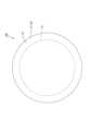
図2は、実施形態1に係る保持装置100の保持基板10(板状部材11)を平面視した状態を模式的に表した説明図である。図2に示されるように、板状部材11を平面視した状態において、第1表面S1に対する電極層12の面積比率が80%以上となっている。電極層12は、図2に示されるように、平面視で略円形状をなしており、第1表面S1の大部分と重なるように、板状部材11の内部に配置されている。Figure 2 is an explanatory diagram that shows a schematic plan view of the holding substrate 10 (plate-shaped member 11) of the
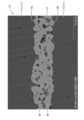
図3は、厚み方向に沿った板状部材11中の電極層12の切断面のSEM画像を示す図である。図3に示されるように、本実施形態の場合、電極層12の第1表面S1側(上側)における表面12aは、粗化されている。つまり、電極層12の表面12aは、多数の凸部と多数の凹部とを含む凹凸面となっている。Figure 3 is a diagram showing an SEM image of a cut surface of the
このような電極層12の第1表面S1側における表面12aのフラクタル次元Dは、1.18以上となっている。電極層12の表面12aにおけるフラクタル次元は、ボックスカウント法により求められる。The fractal dimension D of the
フラクタル次元Dが、1.18以上とは、電極層12の表面12a形状が複雑であることを意味している。フラクタル次元とは、幾何学的な複雑さの指標であり、本実施形態では、電極層12を切断面でみたときのフラクタル次元(即ち、2次元のフラクタル次元)を規定している。なお、一般的に、2次元のフラクタル次元において、例えば、輪郭形状が、真円、正方形、長方形等のシンプルな形状の場合のフラクタル次元は、約1となり、多数の凹凸を有する形状等、形状が複雑になるほどフラクタル次元は大きくなり、2に近付くことが知られている。A fractal dimension D of 1.18 or more means that the shape of the
ここで、ボックスカウント法によるフラクタル次元の解析方法(原理)を、簡単に説明する。例えば、ある平面内に存在する図形を、1辺の長さがdの正方形で分割するとき、その図形がN(d)個の正方形で覆われていたとすると、N(d)とdとの間に、
N(d)=ad-D (aは正の整数) ・・・(I)
という関係が成り立つとき、Dをその図形のフラクタル次元と定義する。
更に、上記式(I)の両辺の対数をとると、
log10N(d)=-D・log10d+log10a(aは正の整数)・・・(II)
となり、dとN(d)の両対数プロットを描けば、その直線の傾きからフラクタル次元Dを求めることができる。 Here, we will briefly explain the method (principle) of analyzing fractal dimension by the box counting method. For example, when a figure existing in a certain plane is divided into squares with a side length of d, if the figure is covered with N(d) squares, then between N(d) and d,
N(d) = ad- D (a is a positive integer) ... (I)
When the above relationship holds, D is defined as the fractal dimension of the figure.
Furthermore, taking the logarithm of both sides of the above formula (I) gives:
log10 N(d) = -D log10 d + log10 a (a is a positive integer) ... (II)
If a log-log plot of d and N(d) is drawn, the fractal dimension D can be found from the slope of the line.
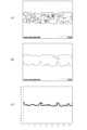
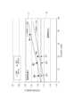
図4は、電極層12の切断面から抽出された表面12aの輪郭線に基づいて、ボックスピクセルサイズ(d)対ボックス数(N(d))について、常用対数プロットしたグラフを示す図である。なお、ボックスカウント法によるフラクタル次元の求め方の詳細は、後述する。Figure 4 shows a graph plotting the box pixel size (d) versus the number of boxes (N(d)) in common logarithms based on the contour of the
本実施形態の場合、電極層12の第2表面S2側(下側)における表面12bは、粗化されておらず、表面12aと比べて、凹凸が小さく、平坦な面となっている。つまり、本実施形態の電極層12は、少なくともウェハWが載せられる第1表面S1側の表面12aが、所望のフラクタル次元Dで表される凹凸面となるように粗化されている。In this embodiment, the
また、本実施形態の場合、厚み方向に沿った電極層12の切断面のうち、電極層12の中心側に設定された観察範囲に対するセラミックスの面積比率が30%以下となっている。In addition, in this embodiment, the area ratio of ceramic to the observation range set on the center side of the
図3のSEM画像に示されるように、電極層12の主成分である導電材料40が、層状をなすように存在している。そして、その層状の導電材料40の内部に、複数のセラミックス(アルミナ)50の塊部分が存在している。ただし、本実施形態の場合、電極層12の切断面において、セラミックス50は、第1誘電層111と第2誘電層112とを繋ぐような形で存在していない。つまり、本実施形態の場合、電極層12(導電材料)を厚み方向に貫通する形で、セラミックス50が存在していない。なお、層状をなした導電材料40の上側の表面が、電極層12の表面12aとなり、導電材料40の下側の表面が、電極層12の表面12bとなる。As shown in the SEM image of FIG. 3, the
セラミックスの前記面積比率が30%以下(好ましくは、25%以下)であると、電極層12が優れた熱伝導性を備える。なお、厚み方向に沿った電極層12の切断面における前記セラミックスの面積比率の算出方法は、後述する。前記面積比率の下限値としては、電極層12と板状部材11との間の密着性確保等の観点より、3%以上が好ましく、5%以上がより好ましい。When the ceramic area ratio is 30% or less (preferably 25% or less), the
なお、保持基板10は、第1表面S1側に不活性ガス(例えば、熱伝導ガスであるヘリウムガス)を供給するためのガス流路等の他の構成を備えていてもよい。The holding
ベース部材20は、例えば、金属(アルミニウム、アルミニウム合金等)、金属とセラミックスの複合体(Al-SiC)、又はセラミックス(SiC)を主成分として構成される。The
ベース部材20の内部には、冷却機構である冷媒流路21が設けられている。冷媒流路21に冷媒(例えば、フッ素系不活性液体、水等)が流されることで、プラズマ熱の冷却が行われる。また、冷媒流路21に冷媒が流されると、ベース部材20が冷却され、接合材30を介したベース部材20と保持基板10との間の伝熱(熱引き)により、保持基板10が冷却される。その結果、保持基板10の第1表面S1で保持されたウェハWが冷却される。なお、冷媒流路21における冷媒流量を適宜、調整することにより、第1表面S1で保持されたウェハWの温度を制御することができる。Inside the
なお、ベース部材20は、不活性ガスを供給するためのガス流路等の他の構成を備えていてもよい。The
接合材30は、例えば、シリコーン系の有機接合剤、無機接合剤、又はAl系の金属接着剤を含むボンディングシート等により構成される。接合材としては、保持基板10及びベース部材20の双方に対して高い接着力を備えつつ、高い耐圧性及び熱伝導性を備えるものが好ましい。なお、接合材30にも、必要に応じて、不活性ガスを供給するためのガス流路が形成されてもよい。The
続いて、本実施形態の保持装置100の製造方法の一例を説明する。ここで、先ず図5を参照しつつ、保持装置100が備える保持基板10の製造方法について説明する。図5は、保持基板10の製造方法を模式的に表した説明図である。この保持基板10の製造方法は、グリーンシート(セラミックグリーンシート)を利用するシート積層法を応用したものである。Next, an example of a method for manufacturing the
先ず、図5(A)に示されるように、板状部材11の第1誘電層111を形成するために、グリーンシートを複数枚積層して、第1積層物111Xが用意される。グリーンシート用のスラリーは、例えば、アルミナ粉末、アクリル系バインダ、分散剤、可塑剤、焼結助剤(例えば、ガラス、希土類酸化物)等を含む混合物に、更に有機溶剤を加えたものを、ボールミルを用いて混合することで得られる。このスラリーを、キャスティング装置でシート状に成形し、その後、得られた成形物を乾燥させることで、複数枚のグリーンシートが得られる。First, as shown in FIG. 5(A), in order to form the
次いで、図5(B)に示されるように、第1積層物111Xの表面111Xaに対して、表面粗化処理が施される。表面粗化処理は、最終的に得られる電極層12の表面12aを、所望のフラクタル次元Dで表される凹凸面となるように粗化することを目的として行われる。表面粗化処理は、電極層12を形成するためのメタライズペースト12Xの表面に対して、直接、行ってもよいし、その表面と接触する相手側(第1積層物111X)の表面111Xaに対して行ってもよい。ここでは、表面粗化処理として、相手側の第1積層物111Xの表面111Xaに対して行う場合を例示する。Next, as shown in FIG. 5(B), the surface 111Xa of the
表面粗化処理としては、所望のフラクタル次元D(1.18以上)が得られるものであれば、特に制限はなく、例えば、サンドブラスト処理、スパッタリング処理、コロナ(放電)処理、火炎処理、紫外線照射処理、電子線照射処理等が施されてもよい。There are no particular limitations on the surface roughening treatment, so long as the desired fractal dimension D (1.18 or more) is obtained, and for example, sandblasting, sputtering, corona (discharge) treatment, flame treatment, ultraviolet irradiation treatment, electron beam irradiation treatment, etc. may be used.
その後、図5(C)に示されるように、表面粗化処理後の第1積層物111Xの表面111Xaに、電極層12を形成するためのメタライズペースト12Xが積層される。メタライズペースト12Xは、アルミナ粉末(副成分)、アクリル系バインダ、有機溶剤の混合物に、タングステンやモリブデン等の導電性粉末(主成分)を添加して混練することで得られる。このメタライズペースト12Xは、例えばスクリーン印刷装置を用いて、第1積層物111Xの表面111Xa上に、層状に形成される。このようにメタライズペースト12Xを層状に形成すると、第1積層物111Xの表面111Xaと接触する表面が、最終的に、所望のフラクタル次元D(1.18以上)で表される凹凸面となる。After that, as shown in FIG. 5(C), a metallization paste 12X for forming an
なお、第1積層物111X上のメタライズペースト12Xを平面視した際、メタライズペースト12Xの周りには、メタライズペースト12Xの周りを取り囲む枠状のグリーンシート(不図示)が配置されている。この枠状のグリーンシートは、第1積層物111Xの表面111Xaのうち、メタライズペースト12Xが形成されていない箇所に配置される。When the metallization paste 12X on the
次いで、図5(D)に示されるように、板状部材11の第2誘電層112を形成するための第2積層物112Xが用意され、その第2積層物112Xが、第1積層物111X上のメタライズペースト12Xに積層される。Next, as shown in FIG. 5(D), a
第2積層物112Xは、上述した第1積層物111Xと同様、グリーンシートを複数枚積層することで形成される。このように形成された第2積層物112Xが、第1積層物111Xとの間でメタライズペースト12Xを挟むように、第1積層物111X上のメタライズペースト12X上に積層される。これらの積層物は、互いに熱圧着される。The
なお、第1積層物111X、メタライズペースト12X及び第2積層物112Xからなる積層物の外周は、適宜、切断されてもよい。そして、前記積層物をマシニングによって切削加工して円板状の成形体が得られる。続いて、得られた成形体を脱脂焼成し、更に、脱脂焼成後の成形体を焼成(本焼成)することで、焼結体が得られる。その後、焼結体の表面に対して、適宜、加工や研磨等を施すことにより、図5(E)に示されるような板状部材11を有する保持基板10が得られる。The outer periphery of the laminate consisting of the
ベース部材20の製造方法は、基本的に従来品の製造方法と同じである。そのため、その詳細説明は省略する。The manufacturing method for the
保持基板10及びベース部材20がそれぞれ作製された後、それらを、接合材30を利用して接合する。接合材30による保持基板10及びベース部材20の接合は、基本的には、従来品における接合と同じである。そのため、詳細説明は省略する。このようにして、保持装置100が製造される。After the holding
以上のように、本実施形態の保持装置100は、高純度のアルミナ(セラミックスの一例)を主成分とする板状部材11と、その内部に配置される電極層12との接着性に優れると共に、抜熱性(熱伝導性)に優れる保持基板11を備えている。As described above, the holding
電極層12は、主成分である導電材料40以外に、所定量のアルミナを副成分として含んでいるため、電極層12の表面12aを、フラクタル次元Dが1.18以上である凹凸面とすることができる。このような電極層12の表面12aは、それに隣接する第1誘電層111の表面との密着性に優れるため、それらの間に熱の移動の妨げとなる隙間(空間)が形成されることが抑制される。Because the
なお、電極層12中のアルミナ量は、比較的、少なく抑えられているため、電極層12は、熱伝導性の劣る、第1誘電層111と第2誘電層112とを繋ぐような形のセラミックス(アルミナ)50を備えず、主に熱伝導性に優れる導電材料40で構成されることになる。そのため、本実施形態の電極層12は、それ自体が熱伝導性に優れている。このような電極層12の表面12a側に積層された第1誘電層111側が、プラズマ処理時に加熱されても、熱は、第1誘電層111から電極層12へ速やかに移動することができる。電極層12へ移動した熱は、第2誘電層112へ移動しつつ、更にベース部材20側へ移動することになる。このような保持基板10を備えた保持装置100は、抜熱性(熱伝導性)に優れる。In addition, since the amount of alumina in the
また、本実施形態の場合、板状部材11を表側(第1表面S1側)から平面視した状態において、第1表面S1に対する電極層12の表面12aの面積比率が80%以上となっているため、電極層12が、保持基板10(保持装置100)の抜熱性(熱伝導性)に与える影響は大きいと言える。In addition, in the case of this embodiment, when the plate-
<実施形態2>
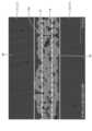
次いで、実施形態2に係る保持装置が備える保持基板10Aを、図6を参照しつつ説明する。図6は、実施形態2の保持基板10Aが備える板状部材11の厚み方向に沿った切断面のSEM画像を示す図である。本実施形態の場合、板状部材11中に形成される電極層12Aの両面が粗化されている。電極層12Aの第1表面側(上側)における表面12Aa、及び第2表面側(下側)における表面12Abは、多数の凸部と多数の凹部とを含む凹凸面となっている。なお、本実施形態の保持装置(保持基板10A)は、電極層12Aの両面が粗化されていること以外、基本的に、実施形態1と同じ構成を備えている。 <
Next, the holding
電極層12Aの表面12Aaのフラクタル次元D、及び電極層12Aの表面12Abのフラクタル次元Dは、共に1.18以上となっている。The fractal dimension D of the surface 12Aa of the
また、本実施形態の場合も、実施形態1と同様、厚み方向に沿った電極層12Aの切断面のうち、電極層12Aの中心側に設定された観察範囲に対するセラミックスの面積比率が30%以下となっている。In the present embodiment, as in the first embodiment, the ceramic area ratio to the observation range set at the center of the
電極層12Aの上側の表面12Aaを粗化する方法としては、例えば、保持基板10Aの製造時、第1誘電層111を形成するためのグリーンシートの第1積層物の表面に対して、上述した表面粗化処理を施すと共に、その第1積層物の表面に、電極層12Aを形成するためのメタライズペーストを積層する方法が挙げられる。One method for roughening the upper surface 12Aa of the
また、電極層12Aの下側の表面12Abを粗化する方法としては、例えば、保持基板10Aの製造時、第2誘電層112を形成するためのグリーンシートの第2積層物の表面に対して、上述した表面粗化処理を施すと共に、その第2積層物の表面を、第1積層物上のメタライズペーストに押し付けるように、第2積層物をメタライズペースト上に積層する方法が挙げられる。As a method for roughening the lower surface 12Ab of the
本実施形態のように、電極層12Aの上側の表面12Aaのみならず、下側の表面12Abについても、所望のフラクタル次元D(1.18以上)で表される凹凸面を備えるように、粗化されてもよい。このように電極層12Aの両面が粗化されることで、更に、本実施形態の保持基板10A(保持装置)の抜熱性(熱伝導性)が優れることになる。As in this embodiment, not only the upper surface 12Aa of the
以下、実施例に基づいて本発明を更に詳細に説明する。なお、本発明はこれらの実施例により何ら限定されるものではない。The present invention will be described in more detail below with reference to examples. Note that the present invention is not limited to these examples.
〔実施例1〕
(メタライズペーストの作製)
アルミナ粉末、アクリル系バインダ、有機溶剤の混合物に、導電性粉末を添加して混練することで、メタライズペーストを作製した。なお、メタライズペースト中のアルミナ粉末の量は、アルミナ粉末と導電性粉末の合計体積100%に対して、20体積%となるように調整した。Example 1
(Preparation of Metallizing Paste)
A metallization paste was prepared by adding conductive powder to a mixture of alumina powder, an acrylic binder, and an organic solvent, and kneading the mixture. The amount of alumina powder in the metallization paste was adjusted to 20% by volume relative to the total volume of the alumina powder and conductive powder, which was 100%.
(グリーンシートの作製)
アルミナ粉末、アクリル系バインダ、分散剤、可塑剤、焼結助剤等を含む混合物に、更に有機溶剤を加えたものを、ボールミルを用いて混合することで、高純度の板状部材(アルミナの含有率:99.5質量%以上)を形成するためのグリーンシート用のスラリーを作製した。(Preparation of green sheets)
A mixture containing alumina powder, acrylic binder, dispersant, plasticizer, sintering aid, etc., to which an organic solvent was further added, was mixed using a ball mill to produce a slurry for green sheets for forming high-purity plate-shaped members (alumina content: 99.5 mass % or more).
(保持基板の作製)
得られたメタライズペーストと、グリーンシート用のスラリーとを使用すること以外は、実施形態1において説明した保持基板の製造方法と同様の方法で、保持基板を模した実施例1のサンプルを作製した。なお、実施例1では、電極層を形成するための層状のメタライズペーストの上側の表面のみに、表面粗化処理により、粗化を施した。(Preparation of holding substrate)
Except for using the obtained metallization paste and the slurry for the green sheet, a sample of Example 1 simulating a holding substrate was produced in the same manner as the manufacturing method of the holding substrate described in the
〔実施例2~4〕
メタライズペースト中のアルミナ粉末の量を、表1に示される値(体積%)に変更したこと以外は、実施例1と同様の方法で、実施例2~4の各サンプルを作製した。なお、実施例2~4では、アルミナの含有率が99.5質量%以上の高純度の板状部材を形成するためのスラリーを作製した。[Examples 2 to 4]
Each sample of Examples 2 to 4 was produced in the same manner as Example 1, except that the amount of alumina powder in the metallizing paste was changed to the value (volume %) shown in Table 1. In Examples 2 to 4, slurries for forming high-purity plate-shaped members with an alumina content of 99.5 mass % or more were produced.
〔比較例1~3〕
メタライズペースト中のアルミナ粉末の量を、表1に示される値(体積%)に変更したこと以外は、比較例1と同様の方法で、比較例1~3の各サンプルを作製した。なお、比較例1~3では、アルミナの含有率が99.5質量%以上の高純度の板状部材を形成するためのスラリーを作製した。Comparative Examples 1 to 3
Each sample of Comparative Examples 1 to 3 was produced in the same manner as Comparative Example 1, except that the amount of alumina powder in the metallizing paste was changed to the value (volume %) shown in Table 1. In Comparative Examples 1 to 3, slurries for forming high-purity plate-shaped members with an alumina content of 99.5 mass % or more were produced.
〔評価〕
各実施例及び各比較例に係る各サンプルについて、以下に示される方法により、「電極層の切断面におけるセラミックスの面積比率」、「電極層の表面のフラクタル次元D」、「密着強度」、「熱伝導率」等を評価した。〔evaluation〕
For each sample relating to each example and each comparative example, the "area ratio of ceramics in the cut surface of the electrode layer,""fractal dimension D of the surface of the electrode layer,""adhesionstrength,""thermalconductivity," etc. were evaluated using the methods described below.
(電極層の切断面におけるセラミックスの面積比率)
保持基板を模したサンプルを、厚み方向に切断し、得られた切断面を研磨した。その後、切断面を、走査電子顕微鏡(SEM)を用いて撮影して、切断面のSEM画像(倍率:3000倍)を得た。図7は、切断面のSEM画像において、電極層12の中心側に設定された観察範囲Rを示す説明図である。観察範囲Rは、図7に示されるように、電極層12の最上部(トップ)を通るように設定された直線状の上側基準線L1と、最下部(ボトム)を通るように設定された直線状の下側基準線L2との間に設定される。上側基準線L1と下側基準線L2とは互いに平行に配されおり、そのような上側基準線L1と下側基準線L2との間の範囲を100%とした場合に、上側基準線L1から下側に30%の部分を除くと共に、下側基準線L2から上側に30%の部分を除いたものが、観察領域Rとなる。つまり、観察領域Rは、上側基準線L1と下側基準線L2との間で挟まれた範囲(100%)のうち、中心側の40%の部分からなる。(Area ratio of ceramics on the cut surface of the electrode layer)
A sample simulating a holding substrate was cut in the thickness direction, and the cut surface was polished. The cut surface was then photographed using a scanning electron microscope (SEM) to obtain an SEM image (magnification: 3000 times) of the cut surface. FIG. 7 is an explanatory diagram showing an observation range R set on the center side of the
その後、前記SEM画像を2値化処理し、得られた2値化画像から、画像処理ソフトを利用して、電極層12を構成する導電材料40と、その導電材料40の内部に存在するセラミックスの部分50とが区別される。そして、更に、画像処理ソフトを利用して、観察範囲R(100%)に対するセラミックスの面積比率が、求められる。観察範囲Rは、1つのサンプルについて、3箇所設定した、前記面積比率は、これら3箇所での平均値として求めた。結果は、表1に示した。The SEM image is then binarized, and the
(フラクタル次元D)
各サンプルにおける電極層の表面のフラクタル次元Dは、以下に示されるボックスカウント法により求めた。図8は、フラクタル次元Dを求める際に行われる画像処理を示す説明図である。先ず、上述した面積比率の評価時に撮影した、電極層の切断面のSEM画像(倍率:3000倍)を、画像処理ソフト(アメリカ国立衛生研究所、Wayne Rasband氏が作成したImageJ)を用いて、2値化処理し、更に、得られた2値化画像から、電極層12(導電材料40)の輪郭線を抽出した。図8(A)に、輪郭線を抽出した画像の一例を示す。なお、図8(A)の下側に示される電極層12の輪郭線が、粗化された表面に対応する。その後、図8(B)に示されるように、前記画像処理ソフトを用いて、輪郭線の内側を塗り潰し、そして、得られた塗り潰し画像から、図8(C)に示されるように、粗化された表面に対応する輪郭線部分を抽出した。なお、図8(C)に示されるように、抽出した輪郭線部分に対して、座標を設定した。(Fractal dimension D)
The fractal dimension D of the surface of the electrode layer in each sample was obtained by the box counting method shown below. FIG. 8 is an explanatory diagram showing the image processing performed when obtaining the fractal dimension D. First, the SEM image (magnification: 3000 times) of the cut surface of the electrode layer taken during the evaluation of the above-mentioned area ratio was binarized using image processing software (ImageJ created by Wayne Rasband, National Institutes of Health, USA), and further, the contour of the electrode layer 12 (conductive material 40) was extracted from the obtained binarized image. FIG. 8(A) shows an example of an image from which the contour is extracted. Note that the contour of the
その後、抽出した前記輪郭線部分について、前記画像処理ソフトのボックスカウンティングツールを用いて、正方形のボックス一辺の長さdを、2~64ピクセル(2,3,4,6,8,12,16,32,64)で段階的に変化させながら、各dの被覆数N(d)を計測した。得られた各正方形のボックス一辺の長さdと、それに対応した被覆数N(d)を、上記式(II)にしたがって、常用対数プロットし、その直線の傾きから、フラクタル次元を算出した。結果は、表1に示した。Then, for the extracted contour portion, the box counting tool of the image processing software was used to measure the number of coverings N(d) for each square box side length d, while gradually changing the length d from 2 to 64 pixels (2, 3, 4, 6, 8, 12, 16, 32, 64). The obtained square box side length d and the corresponding number of coverings N(d) were plotted in common logarithms according to the above formula (II), and the fractal dimension was calculated from the slope of the straight line. The results are shown in Table 1.
(表面粗さRa)
また、参考として、各サンプルにおける電極層の表面粗さ(算術平均粗さ)Raを、JIS B0601-2001に準拠して、図8(C)に示される輪郭部分(粗さ曲線)に基づいて求めた。結果は、表1に示した。(Surface roughness Ra)
For reference, the surface roughness (arithmetic mean roughness) Ra of the electrode layer in each sample was determined based on the contour portion (roughness curve) shown in Figure 8(C) in accordance with JIS B0601-2001. The results are shown in Table 1.
なお、表面粗さRaは、前記輪郭部分(粗さ曲線)からその平均線の方向に基準長さLだけを抜き取り、その抜き取り部分の平均線の方向にX軸、及び縦倍率の方向にY軸をそれぞれ設定した上で、粗さ曲線をy=f(X)で表したときに、以下の式(1)で求められる値を、マイクロメートル(μm)で表したものである。The surface roughness Ra is the value, expressed in micrometers (μm), calculated by the following formula (1) when a reference length L is cut out from the contour portion (roughness curve) in the direction of the average line, the X axis is set in the direction of the average line of the cut out portion, and the Y axis is set in the direction of the longitudinal magnification, and the roughness curve is expressed as y = f(X).

(密着強度)
各実施例等で作製した電極層用のメタライズペーストを使用して、図9に示される試験体TPを作製した。図9は、密着強度の測定に使用される試験体TPを模式的に表した説明図である。図9に示される試験体TPは、凹部を含む試験用の板状部材11Tの表面11Ta上に、試験用の電極層12T、及び導電性電極層(めっき付着用電極層)13Tが形成された積層体からなる。この積層体の導電性電極層13Tには、更に、ニッケルめっき層60T、及びろう材(Ag-Cu)を介して、棒状のコバール端子80Tが固定される。なお、図9には、説明の便宜上、表面粗化された電極層12Tの表面側が、符号12Taで示されている。(Adhesion strength)
A test specimen TP shown in FIG. 9 was prepared using the metallizing paste for the electrode layer prepared in each Example. FIG. 9 is an explanatory diagram that shows a schematic representation of the test specimen TP used for measuring adhesion strength. The test specimen TP shown in FIG. 9 is a laminate in which a
試験用の板状部材11Tは、実施例1等で用意したグリーンシート用のスラリーを用いて作製した。The
実施例1~4の試験体TPについては、上述した保持基板に模したサンプルの作製時と同様、表面粗化処理により粗化された板状部材11Tの表面11Ta上に、電極層12Tが形成されている。For the test specimens TP of Examples 1 to 4, an
以上のようにして作製した試験体TPに対して、株式会社島津製作所製のオートグラフ(精密万能試験機)を用いて、以下に示される方法で、電極層12Tの密着強度を測定した。具体的には、棒状のコバール端子80Tが水平方向に配されるように、試験体TPの積層体側を固定した状態で、根元側から15mm離れた箇所のコバール端子80Tに対して、オートグラフを用いて5mm/minの条件で押し下げるように力を加えた。そして、このように力が加えられることで試験体TPが破壊された際の強度(N)を測定した。各実施例及び各比較例において、それぞれ5回ずつ強度(N)の測定を行った。結果は、図10に示した。図10は、各実施例及び各比較例の電極層の接着強度(N)を測定した結果をまとめたグラフを示す図である。なお、5回の測定結果の平均値を、各実施例等の密着強度(N)とした。そして、密着強度(N)が80N以上の場合を、「密着性あり」とし、密着強度(N)が80N未満を、「密着性なし」とした。表1では、「密着性あり」を符号「○」で表し、「密着性なし」を符号「×」で表した。The adhesion strength of the
(熱伝導率)
各実施例等で作製した電極層用のメタライズペーストを使用して、試験用の電極層を作製した。そして得られた試験用の電極層を用いて、以下に示される方法で、熱伝導率を測定した。結果は、表1に示した。(Thermal Conductivity)
A test electrode layer was prepared using the metallizing paste for the electrode layer prepared in each Example. The thermal conductivity of the obtained test electrode layer was measured by the method described below. The results are shown in Table 1.
電極層用のメタライズペーストを、脱脂後に所定形状に成形し、得られた成形体を焼成して、焼成体を得た。その後、焼成体に対して、適宜、切断・研摩加工を施した後、その焼成体について、JIS R1611に準拠してレーザーフラッシュ法に基づいて熱拡散率と比熱を測定した。また、その焼成体について、JIS R1634に準拠して、嵩密度を測定した。このようにして得られた熱拡散率、比熱及び嵩密度を掛け合わせたものを、熱伝導率とした。The metallization paste for the electrode layer was degreased and molded into a predetermined shape, and the molded body obtained was fired to obtain a fired body. The fired body was then appropriately cut and polished, and the thermal diffusivity and specific heat of the fired body were measured based on the laser flash method in accordance with JIS R1611. The bulk density of the fired body was also measured in accordance with JIS R1634. The thermal diffusivity, specific heat, and bulk density thus obtained were multiplied to obtain the thermal conductivity.

(密着性について)
上述した密着強度の試験の結果、実施例1~4の電極層は、板状部材(高純度のアルミナ)に対する密着性に優れることが確かめられた。実施例1~3の場合、電極層におけるアルミナの含有率(5~20vol%)は、比較的、少ないものの、電極層の表面が所望のフラクタル次元D(1.18以上)となるように、粗化されている。また、実施例4の場合も、電極層の表面が所望のフラクタル次元D(1.18以上)となるように、粗化されている。このような実施例1~4の場合では、オートグラフを用いた密着強度の試験時に、試験体TPの電極層と板状部材との間の界面で破壊は起こらず、電極層の内部で破壊が生じた。(About adhesion)
As a result of the above-mentioned adhesion strength test, it was confirmed that the electrode layers of Examples 1 to 4 have excellent adhesion to the plate-shaped member (high-purity alumina). In the cases of Examples 1 to 3, the alumina content (5 to 20 vol%) in the electrode layer is relatively low, but the surface of the electrode layer is roughened so as to have a desired fractal dimension D (1.18 or more). In the case of Example 4, the surface of the electrode layer is roughened so as to have a desired fractal dimension D (1.18 or more). In the cases of Examples 1 to 4, during the adhesion strength test using an autograph, no destruction occurred at the interface between the electrode layer of the test specimen TP and the plate-shaped member, but destruction occurred inside the electrode layer.
これに対して、比較例1~3の電極層は、板状部材(高純度のアルミナ)に対して、十分な密着性を備えていないことが確かめられた。比較例1~3の場合、電極層におけるアルミナの含有率(5~20vol%)は、比較的、少ないため、電極層の表面が所望のフラクタル次元Dとなるように粗化されていないと、板状部材に対して十分な密着性を発揮できないと言える。なお、比較例1~3の場合では、オートグラフを用いた密着強度の試験時に、試験体TPの電極層と板状部材との間の界面で破壊が生じた。In contrast, it was confirmed that the electrode layers of Comparative Examples 1 to 3 did not have sufficient adhesion to the plate-shaped member (high-purity alumina). In the cases of Comparative Examples 1 to 3, the alumina content (5 to 20 vol%) in the electrode layer was relatively low, so unless the surface of the electrode layer was roughened to have the desired fractal dimension D, it could not exhibit sufficient adhesion to the plate-shaped member. In the cases of Comparative Examples 1 to 3, destruction occurred at the interface between the electrode layer of the test specimen TP and the plate-shaped member during adhesion strength testing using an autograph.
(熱伝導性について)
表1に示されるように、電極層におけるアルミナの含有率が多くなるにつれて、電極層の熱伝導率が低下することが確かめられた。特に、実施例1~4の中でも、実施例1~3の電極層は、熱伝導率が60W/mK以上であり、熱伝導性に優れる。なお、比較例1~3の電極層については、上述したように、板状部材に対する密着性は十分でないものも、熱伝導性に優れる。(Thermal conductivity)
As shown in Table 1, it was confirmed that the thermal conductivity of the electrode layer decreases as the alumina content in the electrode layer increases. In particular, among Examples 1 to 4, the electrode layers of Examples 1 to 3 have a thermal conductivity of 60 W/mK or more and are excellent in thermal conductivity. As for the electrode layers of Comparative Examples 1 to 3, as described above, they have excellent thermal conductivity even though they do not have sufficient adhesion to the plate-like member.
(フラクタル次元Dと密着性との関係)
ここで、図11に、各実施例及び各比較例における電極層のフラクタル次元Dと、電極層の密着性との関係をグラフにまとめた。図11のグラフの縦軸は、フラクタル次元Dを表し、横軸は、電極層に含まれるアルミナの含有率(vol%)を表す。そして、図11のグラフ中において、各実施例及び各比較例を、電極層の密着強度が80N以上の場合(密着性あり)と、電極層の密着強度が80N未満の場合(密着性なし)とに、フラクタル次元Dに基づいて区別すると、図11に示されるような範囲Z1(密着性あり)及び範囲Z2(密着性なし)を設定することができる。これらの範囲Z1及び範囲Z2は、フラクタル次元Dが1.18の付近で区別することができる。このような図11のグラフより、電極層の表面のフラクタル次元Dが1.18以上であると、電極層の密着強度が確保されると言える。(Relationship between fractal dimension D and adhesion)
Here, FIG. 11 shows a graph of the relationship between the fractal dimension D of the electrode layer in each example and each comparative example and the adhesion of the electrode layer. The vertical axis of the graph in FIG. 11 represents the fractal dimension D, and the horizontal axis represents the content (vol%) of alumina contained in the electrode layer. In the graph in FIG. 11, when each example and each comparative example are classified into a case where the adhesion strength of the electrode layer is 80N or more (with adhesion) and a case where the adhesion strength of the electrode layer is less than 80N (without adhesion) based on the fractal dimension D, it is possible to set the range Z1 (with adhesion) and the range Z2 (without adhesion) as shown in FIG. 11. These ranges Z1 and Z2 can be distinguished when the fractal dimension D is in the vicinity of 1.18. From the graph in FIG. 11, it can be said that the adhesion strength of the electrode layer is ensured when the fractal dimension D of the surface of the electrode layer is 1.18 or more.
なお、図11のグラフに示されるように、電極層中のアルミナの含有率(vol%)が大きくなると、電極層の表面におけるフラクタル次元Dが大きくなる傾向がある。また、図11のグラフに示されるように、電極層の表面が粗化されている方が、粗化されていない場合よりも、フラクタル次元Dが大きくなる。As shown in the graph of FIG. 11, the fractal dimension D of the surface of the electrode layer tends to increase as the alumina content (vol%) in the electrode layer increases. Also, as shown in the graph of FIG. 11, the fractal dimension D is larger when the surface of the electrode layer is roughened than when it is not roughened.
(表面粗さRaと密着性との関係)
参考として、図12に、各実施例及び各比較例における電極層の表面粗さRaと、電極層の密着性との関係をグラフにまとめた。図12のグラフの縦軸は、表面粗さRaを表し、横軸は、電極層に含まれるアルミナの含有率(vol%)を表す。このようなグラフにおいて、各実施例及び各比較例を、電極層の密着強度が80N以上の場合(密着性あり)と、電極層の密着強度が80N未満の場合(密着性なし)とに、表面粗さRaに基づいて区別しようとしても、それらを区別することができない。つまり、電極層の密着性は、表面粗さRaではなく、フラクタル次元Dで表す必要がある。(Relationship between surface roughness Ra and adhesion)
For reference, FIG. 12 shows a graph of the relationship between the surface roughness Ra of the electrode layer in each example and each comparative example and the adhesion of the electrode layer. The vertical axis of the graph in FIG. 12 represents the surface roughness Ra, and the horizontal axis represents the content (vol%) of alumina contained in the electrode layer. In such a graph, even if one tries to distinguish between the examples and the comparative examples based on the surface roughness Ra, when the adhesion strength of the electrode layer is 80 N or more (with adhesion) and when the adhesion strength of the electrode layer is less than 80 N (without adhesion), it is not possible to distinguish them. In other words, the adhesion of the electrode layer needs to be expressed by the fractal dimension D, not by the surface roughness Ra.
10…保持基板、11…板状部材、12…電極層、20…ベース部材、21…冷媒流路、30…接合材、40…導電材料、50…セラミックス、100…保持装置、111…第1誘電層、112…第2誘電層、R…観察範囲、S1…第1表面、S2…第2表面、S3…第3表面、S4…第4表面10...holding substrate, 11...plate-like member, 12...electrode layer, 20...base member, 21...coolant flow path, 30...bonding material, 40...conductive material, 50...ceramics, 100...holding device, 111...first dielectric layer, 112...second dielectric layer, R...observation area, S1...first surface, S2...second surface, S3...third surface, S4...fourth surface
Claims (4)
Translated fromJapanese前記板状部材は、前記電極層の前記第1表面側に配置され、前記主成分の含有率が99質量%以上である第1誘電層と、前記電極層の前記第2表面側に配置され、前記主成分の含有率が99質量%以上である第2誘電層とを含み、
前記電極層の前記第1表面側における表面のフラクタル次元Dが1.18以上である保持装置。 A holding device comprising a holding substrate having a plate-shaped member including a first surface for holding an object and a second surface disposed on the opposite side of the first surface, the plate-shaped member containing ceramics as a main component, and an electrode layer disposed inside the plate-shaped member, the electrode layer containing a conductive material as a main component and the ceramics as a sub-component,
the plate-like member includes a first dielectric layer disposed on the first surface side of the electrode layer, the first dielectric layer having a content of the main component of 99% by mass or more, and a second dielectric layer disposed on the second surface side of the electrode layer, the second dielectric layer having a content of the main component of 99% by mass or more,
A holding device, wherein the fractal dimension D of the surface on the first surface side of the electrode layer is 1.18 or more.
Priority Applications (5)
| Application Number | Priority Date | Filing Date | Title |
|---|---|---|---|
| JP2023129159AJP7682232B2 (en) | 2023-08-08 | 2023-08-08 | holding device |
| CN202410899166.5ACN119480599A (en) | 2023-08-08 | 2024-07-05 | Holding device |
| KR1020240091041AKR20250022604A (en) | 2023-08-08 | 2024-07-10 | Holding device |
| US18/787,424US20250054799A1 (en) | 2023-08-08 | 2024-07-29 | Holding apparatus |
| TW113129149ATW202516680A (en) | 2023-08-08 | 2024-08-05 | Holding device |
Applications Claiming Priority (1)
| Application Number | Priority Date | Filing Date | Title |
|---|---|---|---|
| JP2023129159AJP7682232B2 (en) | 2023-08-08 | 2023-08-08 | holding device |
Publications (2)
| Publication Number | Publication Date |
|---|---|
| JP2025024834A JP2025024834A (en) | 2025-02-21 |
| JP7682232B2true JP7682232B2 (en) | 2025-05-23 |
Family
ID=94482576
Family Applications (1)
| Application Number | Title | Priority Date | Filing Date |
|---|---|---|---|
| JP2023129159AActiveJP7682232B2 (en) | 2023-08-08 | 2023-08-08 | holding device |
Country Status (5)
| Country | Link |
|---|---|
| US (1) | US20250054799A1 (en) |
| JP (1) | JP7682232B2 (en) |
| KR (1) | KR20250022604A (en) |
| CN (1) | CN119480599A (en) |
| TW (1) | TW202516680A (en) |
Citations (5)
| Publication number | Priority date | Publication date | Assignee | Title |
|---|---|---|---|---|
| JP2004349612A (en) | 2003-05-26 | 2004-12-09 | Kyocera Corp | Electrostatic chuck |
| JP2005343733A (en) | 2004-06-02 | 2005-12-15 | Ngk Insulators Ltd | Method for manufacturing sintered compact with built-in electrode |
| JP2006060040A (en) | 2004-08-20 | 2006-03-02 | Rasa Ind Ltd | Electrostatically chucking plate, and manufacturing method thereof |
| JP2013077702A (en) | 2011-09-30 | 2013-04-25 | Fujifilm Corp | Copper foil for lamination |
| JP2020004748A (en) | 2018-06-25 | 2020-01-09 | 日本特殊陶業株式会社 | Electrostatic chuck |
Family Cites Families (1)
| Publication number | Priority date | Publication date | Assignee | Title |
|---|---|---|---|---|
| JPS5552851Y2 (en) | 1977-08-29 | 1980-12-08 |
- 2023
- 2023-08-08JPJP2023129159Apatent/JP7682232B2/enactiveActive
- 2024
- 2024-07-05CNCN202410899166.5Apatent/CN119480599A/enactivePending
- 2024-07-10KRKR1020240091041Apatent/KR20250022604A/enactivePending
- 2024-07-29USUS18/787,424patent/US20250054799A1/enactivePending
- 2024-08-05TWTW113129149Apatent/TW202516680A/enunknown
Patent Citations (5)
| Publication number | Priority date | Publication date | Assignee | Title |
|---|---|---|---|---|
| JP2004349612A (en) | 2003-05-26 | 2004-12-09 | Kyocera Corp | Electrostatic chuck |
| JP2005343733A (en) | 2004-06-02 | 2005-12-15 | Ngk Insulators Ltd | Method for manufacturing sintered compact with built-in electrode |
| JP2006060040A (en) | 2004-08-20 | 2006-03-02 | Rasa Ind Ltd | Electrostatically chucking plate, and manufacturing method thereof |
| JP2013077702A (en) | 2011-09-30 | 2013-04-25 | Fujifilm Corp | Copper foil for lamination |
| JP2020004748A (en) | 2018-06-25 | 2020-01-09 | 日本特殊陶業株式会社 | Electrostatic chuck |
Also Published As
| Publication number | Publication date |
|---|---|
| KR20250022604A (en) | 2025-02-17 |
| TW202516680A (en) | 2025-04-16 |
| US20250054799A1 (en) | 2025-02-13 |
| JP2025024834A (en) | 2025-02-21 |
| CN119480599A (en) | 2025-02-18 |
Similar Documents
| Publication | Publication Date | Title |
|---|---|---|
| JP5441020B1 (en) | Electrostatic chuck | |
| JP3323135B2 (en) | Electrostatic chuck | |
| KR101452245B1 (en) | Electrostatic chuck | |
| WO2006001425A1 (en) | Electrostatic chuck | |
| KR20140034687A (en) | Electrostatic chuck | |
| JP2000243821A (en) | Wafer support member | |
| JP7682232B2 (en) | holding device | |
| JP2010034256A (en) | Electrostatic chuck | |
| JP3728078B2 (en) | Plasma generating material | |
| JP6629624B2 (en) | Manufacturing method of ceramic heater | |
| JP7400854B2 (en) | Electrostatic chuck member, electrostatic chuck device, and method for manufacturing electrostatic chuck member | |
| JP2016018906A (en) | Electrode-buried body | |
| JP5284227B2 (en) | Electrostatic chuck and method for manufacturing electrostatic chuck | |
| JPWO2007000963A1 (en) | Method for manufacturing ceramic substrate having steps | |
| JP7038496B2 (en) | Parts for semiconductor manufacturing equipment and methods for manufacturing parts for semiconductor manufacturing equipment | |
| JP6154248B2 (en) | Channel member, heat exchanger using the same, and semiconductor manufacturing apparatus | |
| JP4069875B2 (en) | Wafer holding member | |
| JP2017017095A (en) | Passage member and heat exchanger using the same and semiconductor manufacturing equipment | |
| JP2025070758A (en) | Multilayer resistor and method for manufacturing the same | |
| WO2024009768A1 (en) | Holding device | |
| WO2024154827A1 (en) | Silicon nitride substrate and silicon nitride circuit board using same | |
| JP2023138085A (en) | Electrostatic chuck member and electrostatic chuck device | |
| JP2025152517A (en) | Electrostatic chuck device, base manufacturing method, and electrostatic chuck device manufacturing method | |
| WO2023120258A1 (en) | Electrostatic chuck member, electrostatic chuck device, and production method for electrostatic chuck member | |
| JP2004327563A (en) | Electrostatic chuck |
Legal Events
| Date | Code | Title | Description |
|---|---|---|---|
| A621 | Written request for application examination | Free format text:JAPANESE INTERMEDIATE CODE: A621 Effective date:20240926 | |
| A871 | Explanation of circumstances concerning accelerated examination | Free format text:JAPANESE INTERMEDIATE CODE: A871 Effective date:20240926 | |
| A131 | Notification of reasons for refusal | Free format text:JAPANESE INTERMEDIATE CODE: A131 Effective date:20241217 | |
| A521 | Request for written amendment filed | Free format text:JAPANESE INTERMEDIATE CODE: A523 Effective date:20250130 | |
| TRDD | Decision of grant or rejection written | ||
| A01 | Written decision to grant a patent or to grant a registration (utility model) | Free format text:JAPANESE INTERMEDIATE CODE: A01 Effective date:20250508 | |
| A61 | First payment of annual fees (during grant procedure) | Free format text:JAPANESE INTERMEDIATE CODE: A61 Effective date:20250513 | |
| R150 | Certificate of patent or registration of utility model | Ref document number:7682232 Country of ref document:JP Free format text:JAPANESE INTERMEDIATE CODE: R150 |