JP7679931B2 - HEAT DISSIPATION ASSEMBLY, ELECTRONIC DEVICE, AND CHIP PACKAGE STRUCTURE - Google Patents
HEAT DISSIPATION ASSEMBLY, ELECTRONIC DEVICE, AND CHIP PACKAGE STRUCTUREDownload PDFInfo
- Publication number
- JP7679931B2 JP7679931B2JP2023526276AJP2023526276AJP7679931B2JP 7679931 B2JP7679931 B2JP 7679931B2JP 2023526276 AJP2023526276 AJP 2023526276AJP 2023526276 AJP2023526276 AJP 2023526276AJP 7679931 B2JP7679931 B2JP 7679931B2
- Authority
- JP
- Japan
- Prior art keywords
- heat dissipation
- frame body
- heat spreader
- dissipation assembly
- heat
- Prior art date
- Legal status (The legal status is an assumption and is not a legal conclusion. Google has not performed a legal analysis and makes no representation as to the accuracy of the status listed.)
- Active
Links
Images


Classifications
- H—ELECTRICITY
- H05—ELECTRIC TECHNIQUES NOT OTHERWISE PROVIDED FOR
- H05K—PRINTED CIRCUITS; CASINGS OR CONSTRUCTIONAL DETAILS OF ELECTRIC APPARATUS; MANUFACTURE OF ASSEMBLAGES OF ELECTRICAL COMPONENTS
- H05K7/00—Constructional details common to different types of electric apparatus
- H05K7/20—Modifications to facilitate cooling, ventilating, or heating
- H05K7/2039—Modifications to facilitate cooling, ventilating, or heating characterised by the heat transfer by conduction from the heat generating element to a dissipating body
- G—PHYSICS
- G06—COMPUTING OR CALCULATING; COUNTING
- G06F—ELECTRIC DIGITAL DATA PROCESSING
- G06F1/00—Details not covered by groups G06F3/00 - G06F13/00 and G06F21/00
- G06F1/16—Constructional details or arrangements
- G06F1/20—Cooling means
- H—ELECTRICITY
- H01—ELECTRIC ELEMENTS
- H01L—SEMICONDUCTOR DEVICES NOT COVERED BY CLASS H10
- H01L23/00—Details of semiconductor or other solid state devices
- H01L23/02—Containers; Seals
- H01L23/04—Containers; Seals characterised by the shape of the container or parts, e.g. caps, walls
- H—ELECTRICITY
- H01—ELECTRIC ELEMENTS
- H01L—SEMICONDUCTOR DEVICES NOT COVERED BY CLASS H10
- H01L23/00—Details of semiconductor or other solid state devices
- H01L23/28—Encapsulations, e.g. encapsulating layers, coatings, e.g. for protection
- H01L23/31—Encapsulations, e.g. encapsulating layers, coatings, e.g. for protection characterised by the arrangement or shape
- H01L23/3107—Encapsulations, e.g. encapsulating layers, coatings, e.g. for protection characterised by the arrangement or shape the device being completely enclosed
- H—ELECTRICITY
- H01—ELECTRIC ELEMENTS
- H01L—SEMICONDUCTOR DEVICES NOT COVERED BY CLASS H10
- H01L23/00—Details of semiconductor or other solid state devices
- H01L23/34—Arrangements for cooling, heating, ventilating or temperature compensation ; Temperature sensing arrangements
- H01L23/36—Selection of materials, or shaping, to facilitate cooling or heating, e.g. heatsinks
- H01L23/367—Cooling facilitated by shape of device
- H01L23/3672—Foil-like cooling fins or heat sinks
- H—ELECTRICITY
- H01—ELECTRIC ELEMENTS
- H01L—SEMICONDUCTOR DEVICES NOT COVERED BY CLASS H10
- H01L23/00—Details of semiconductor or other solid state devices
- H01L23/34—Arrangements for cooling, heating, ventilating or temperature compensation ; Temperature sensing arrangements
- H01L23/36—Selection of materials, or shaping, to facilitate cooling or heating, e.g. heatsinks
- H01L23/367—Cooling facilitated by shape of device
- H01L23/3675—Cooling facilitated by shape of device characterised by the shape of the housing
- H—ELECTRICITY
- H01—ELECTRIC ELEMENTS
- H01L—SEMICONDUCTOR DEVICES NOT COVERED BY CLASS H10
- H01L23/00—Details of semiconductor or other solid state devices
- H01L23/34—Arrangements for cooling, heating, ventilating or temperature compensation ; Temperature sensing arrangements
- H01L23/40—Mountings or securing means for detachable cooling or heating arrangements ; fixed by friction, plugs or springs
- H01L23/4093—Snap-on arrangements, e.g. clips
- H—ELECTRICITY
- H05—ELECTRIC TECHNIQUES NOT OTHERWISE PROVIDED FOR
- H05K—PRINTED CIRCUITS; CASINGS OR CONSTRUCTIONAL DETAILS OF ELECTRIC APPARATUS; MANUFACTURE OF ASSEMBLAGES OF ELECTRICAL COMPONENTS
- H05K7/00—Constructional details common to different types of electric apparatus
- H05K7/20—Modifications to facilitate cooling, ventilating, or heating
- H05K7/2039—Modifications to facilitate cooling, ventilating, or heating characterised by the heat transfer by conduction from the heat generating element to a dissipating body
- H05K7/20436—Inner thermal coupling elements in heat dissipating housings, e.g. protrusions or depressions integrally formed in the housing
- H05K7/20445—Inner thermal coupling elements in heat dissipating housings, e.g. protrusions or depressions integrally formed in the housing the coupling element being an additional piece, e.g. thermal standoff
- H—ELECTRICITY
- H05—ELECTRIC TECHNIQUES NOT OTHERWISE PROVIDED FOR
- H05K—PRINTED CIRCUITS; CASINGS OR CONSTRUCTIONAL DETAILS OF ELECTRIC APPARATUS; MANUFACTURE OF ASSEMBLAGES OF ELECTRICAL COMPONENTS
- H05K7/00—Constructional details common to different types of electric apparatus
- H05K7/20—Modifications to facilitate cooling, ventilating, or heating
- H05K7/2039—Modifications to facilitate cooling, ventilating, or heating characterised by the heat transfer by conduction from the heat generating element to a dissipating body
- H05K7/20436—Inner thermal coupling elements in heat dissipating housings, e.g. protrusions or depressions integrally formed in the housing
- H05K7/2049—Pressing means used to urge contact, e.g. springs
- H—ELECTRICITY
- H01—ELECTRIC ELEMENTS
- H01L—SEMICONDUCTOR DEVICES NOT COVERED BY CLASS H10
- H01L23/00—Details of semiconductor or other solid state devices
- H01L23/34—Arrangements for cooling, heating, ventilating or temperature compensation ; Temperature sensing arrangements
- H01L23/40—Mountings or securing means for detachable cooling or heating arrangements ; fixed by friction, plugs or springs
- H01L23/4006—Mountings or securing means for detachable cooling or heating arrangements ; fixed by friction, plugs or springs with bolts or screws
- H01L2023/4075—Mechanical elements
- H01L2023/4081—Compliant clamping elements not primarily serving heat-conduction
- H—ELECTRICITY
- H01—ELECTRIC ELEMENTS
- H01L—SEMICONDUCTOR DEVICES NOT COVERED BY CLASS H10
- H01L23/00—Details of semiconductor or other solid state devices
- H01L23/34—Arrangements for cooling, heating, ventilating or temperature compensation ; Temperature sensing arrangements
- H01L23/40—Mountings or securing means for detachable cooling or heating arrangements ; fixed by friction, plugs or springs
- H01L23/4006—Mountings or securing means for detachable cooling or heating arrangements ; fixed by friction, plugs or springs with bolts or screws
- H01L2023/4075—Mechanical elements
- H01L2023/4087—Mounting accessories, interposers, clamping or screwing parts
- H—ELECTRICITY
- H01—ELECTRIC ELEMENTS
- H01L—SEMICONDUCTOR DEVICES NOT COVERED BY CLASS H10
- H01L23/00—Details of semiconductor or other solid state devices
- H01L23/34—Arrangements for cooling, heating, ventilating or temperature compensation ; Temperature sensing arrangements
- H01L23/40—Mountings or securing means for detachable cooling or heating arrangements ; fixed by friction, plugs or springs
- H01L23/4006—Mountings or securing means for detachable cooling or heating arrangements ; fixed by friction, plugs or springs with bolts or screws
Landscapes
- Engineering & Computer Science (AREA)
- Physics & Mathematics (AREA)
- Microelectronics & Electronic Packaging (AREA)
- General Physics & Mathematics (AREA)
- Power Engineering (AREA)
- Computer Hardware Design (AREA)
- Condensed Matter Physics & Semiconductors (AREA)
- Thermal Sciences (AREA)
- Materials Engineering (AREA)
- Chemical & Material Sciences (AREA)
- Theoretical Computer Science (AREA)
- General Engineering & Computer Science (AREA)
- Human Computer Interaction (AREA)
- Cooling Or The Like Of Semiconductors Or Solid State Devices (AREA)
- Cooling Or The Like Of Electrical Apparatus (AREA)
Description
Translated fromJapanese [関連出願への相互参照]
本願は、2020年11月10日付けで中国国家知識財産局に出願された中国特許出願第202011244298.2号、名称「HEAT DISSIPATION ASSEMBLY, ELECTRONIC DEVICE, AND CHIP PACKAGE STRUCTURE」の優先権を主張し、これは参照により本願に組み込まれる。 CROSS-REFERENCE TO RELATED APPLICATIONS
This application claims priority to Chinese Patent Application No. 202011244298.2, entitled "HEAT DISSIPATION ASSEMBLY, ELECTRONIC DEVICE, AND CHIP PACKAGE STRUCTURE," filed with the China State Intellectual Property Office on November 10, 2020, which is incorporated herein by reference.
本願は、放熱技術の分野に関し、特に放熱アセンブリ、電子デバイス、及びチップパッケージ構造に関する。This application relates to the field of heat dissipation technology, and in particular to heat dissipation assemblies, electronic devices, and chip package structures.
電子デバイスの継続的な発展に伴い、人々はますます高度なチップ集積を必要とし、チップの電力消費量も増大している。その結果、チップの放熱が非常に限られており、課題となっている。チップ構造は、図1に示されてよい。チップは概して、基板11、基板11に固定されたダイ12、及び保護カバー13を含んでいる。保護カバー13は、熱伝導材料を使用することによりダイ12に接合されている。With the continuous development of electronic devices, people require more and more high chip integration, and the power consumption of chips is also increasing. As a result, the heat dissipation of chips is very limited and becomes a challenge. The chip structure may be shown in FIG. 1. The chip generally includes a
チップの表面実装技術(SMT)において、高温のリフロープロセスは、高温抵抗性能及び熱伝導材料の接着性が良好であることを必要とする。しかしながら、良好な接着性を有し、高温抵抗性である熱伝導材料は、概しておよそ2W/mKしかない低い熱伝導係数を有しており、チップの放熱要件を満たすことができない。結果として、チップの放熱の問題が、ますます明らかになっている。In chip surface mount technology (SMT), the high temperature reflow process requires good high temperature resistance performance and adhesion of thermal conductive materials. However, thermal conductive materials with good adhesion and high temperature resistance generally have a low thermal conductivity coefficient of only about 2 W/mK, which cannot meet the heat dissipation requirements of chips. As a result, the problem of heat dissipation of chips is becoming more and more obvious.
本願は、要素の放熱効率を改善するために、放熱アセンブリ、電子デバイス、及びパッケージ構造を提供する。要素は、電子的要素、光学的要素、光電子的要素などを含むが、これらに限定されない。The present application provides heat dissipation assemblies, electronic devices, and package structures to improve the heat dissipation efficiency of elements, including but not limited to electronic elements, optical elements, optoelectronic elements, and the like.
第1の態様によれば、本願は、要素の放熱アセンブリを提供する。放熱アセンブリは、ヒートスプレッダ、フレームボディ、及び弾性構造部を含む。ヒートスプレッダは、要素に接触するように構成されており、要素によって生成された熱を均等に伝導することができる。フレームボディは、ヒートスプレッダの位置を制限するように構成されている。フレームボディは、ヒートスプレッダの側壁を取り囲んでおり、ヒートスプレッダが水平方向に移動するのを防止することができ、それによりヒートスプレッダの移動によって発生する放熱境界面の損傷が回避される。弾性構造部は、フレームボディに固着接続されており、弾性構造部は、ヒートスプレッダのうちの、接触予定の要素から離れる方に向いた側面に位置している。弾性構造部は、電子デバイス内の別のコンポーネントに接触し、それにより変形してよく、それにより要素、ヒートスプレッダ、及びフレームボディが、厚さ方向において確実に固定されて、要素によって生成された熱を円滑に伝導できることが確保される。According to a first aspect, the present application provides a heat dissipation assembly for an element. The heat dissipation assembly includes a heat spreader, a frame body, and an elastic structure. The heat spreader is configured to contact the element and can evenly conduct heat generated by the element. The frame body is configured to limit the position of the heat spreader. The frame body surrounds the side walls of the heat spreader and can prevent the heat spreader from moving in a horizontal direction, thereby avoiding damage to the heat dissipation interface caused by the movement of the heat spreader. The elastic structure is fixedly connected to the frame body, and the elastic structure is located on a side of the heat spreader facing away from the element to be contacted. The elastic structure may contact another component in the electronic device and be deformed thereby, thereby ensuring that the element, the heat spreader, and the frame body are securely fixed in the thickness direction to smoothly conduct heat generated by the element.
例えば、要素はチップである。本願のこの実施形態における放熱アセンブリでは、製造プロセスにおいて、チップに対して最初に表面実装技術が実行されてよく、次いで、チップの表面が熱伝導材料でコーティングされ、次いで、放熱アセンブリが取り付けられる。したがって、熱伝導材料の接着強度に対する要件が低減され、それにより、より良好な放熱性能を有する熱伝導材料を選択することができる。このように、要素及び放熱アセンブリの間の熱抵抗が小さく、それによりチップの放熱効率がさらに改善される。For example, the element is a chip. In the heat dissipation assembly in this embodiment of the present application, in the manufacturing process, surface mounting technology may be performed on the chip first, then the surface of the chip is coated with a thermal conductive material, and then the heat dissipation assembly is attached. Therefore, the requirements for the adhesive strength of the thermal conductive material are reduced, so that a thermal conductive material with better heat dissipation performance can be selected. In this way, the thermal resistance between the element and the heat dissipation assembly is small, which further improves the heat dissipation efficiency of the chip.
可能な実装形態では、フレームボディの縁部の少なくとも一部分が、ヒートスプレッダの表面の縁部の方に曲がっており、それによりフレームボディは、ヒートスプレッダの位置を垂直方向において制限することができる。加えて、ヒートスプレッダに対するフレームボディの被覆面積が小さく、それによりヒートスプレッダの熱伝導性能は影響を受けない。In a possible implementation, at least a portion of the edge of the frame body is bent toward the edge of the surface of the heat spreader, so that the frame body can limit the position of the heat spreader in the vertical direction. In addition, the coverage area of the frame body relative to the heat spreader is small, so that the thermal conduction performance of the heat spreader is not affected.
可能な実装形態において、フレームボディは、接触予定の要素の側壁を取り囲み、接触予定の要素にクランプ留めされるように構成されている。この配置により、ヒートスプレッダは要素の表面に固定されることが可能であり、それにより要素、ヒートスプレッダ、及びフレームボディは、水平方向において容易に移動しない。これにより、要素及びヒートスプレッダの間の放熱境界面の安定性がさらに確保される。In a possible implementation, the frame body is configured to surround the sidewalls of the element to be contacted and to be clamped to the element to be contacted. This arrangement allows the heat spreader to be fixed to the surface of the element, so that the element, heat spreader, and frame body do not easily move in the horizontal direction. This further ensures the stability of the heat dissipation interface between the element and the heat spreader.
可能な実装形態において、フレームボディのうちの、ヒートスプレッダからより遠くに離れた面の縁部は、接触予定の要素の表面と面一になる。この配置により、フレームボディ及び要素の間の接触面積が大きくなり、それによりフレームボディ及び要素の間のクランプ留め効果がより良好になる。加えて、フレームボディの縁部は、要素のうちの、ヒートスプレッダから離れる方に向いた面の表面を越えず、それによりフレームボディは、要素の位置にさらに容易に取り付けられることが可能である。さらに、フレームボディは要素の面積を占有せず、要素の周りの空間は、フレームボディを収容するのに十分である。 In a possible implementation, the edge of the frame body onthe side farther away from the heat spreader is flush with the surface of the element to be contacted. This arrangement increases the contact area between the frame body and the element, which leads to a better clamping effect between the frame body and the element. In addition, the edge of the frame body does not extend beyond the surface ofthe side of the element facing away from the heat spreader, which allows the frame body to be more easily attached to the element's location. Furthermore, the frame body does not occupy the area of the element, and the space around the element is sufficient to accommodate the frame body.
可能な実装形態において、フレームボディ及び要素の間のクランプ力を増大させるために、内部に向かって突出した突出構造部が、フレームボディの側壁に配置されてよい。フレームボディ、ヒートスプレッダ、及び要素が、水平方向において確実に固定されることを確保するために、要素は、突出構造部を使用することによって保持されることが可能である。In a possible implementation, a protruding structure protruding inward may be disposed on the side wall of the frame body to increase the clamping force between the frame body and the element. To ensure that the frame body, the heat spreader, and the element are securely fixed in the horizontal direction, the element can be held by using the protruding structure.
可能な実装形態において、突出構造部は、ヒートスプレッダのうちの、弾性構造部から離れる方に向いた面に位置している。要素及びヒートスプレッダが、水平方向において移動しないことを確保するために、要素の位置は、突出構造部を使用することによって制限されてよい。加えて、このように、フレームボディは、より容易にクランプ留めされるように要素に接触することができ、フレームボディ及び要素の間のクランプ力が増大し、それにより要素はより移動しにくくなる。 In a possible implementation, the protruding structure is located on the surface of the heat spreader facing away from the elastic structure. To ensure that the element and the heat spreader do not move in the horizontal direction, the position of the element may be limited by using the protruding structure. In addition, in this way, theframe body can contact the element to be clamped more easily, and the clamping force between the frame body and the element is increased, so that the element is less likely to move.
可能な実装形態において、フレームボディの少なくとも2つの対向する側壁に、突出構造部が存在している。例えば、突出構造部は、フレームボディのすべての4つの側壁に存在しているか、又は突出構造部は、フレームボディの2つの対向する側壁に存在している。このように、フレームボディのクランプ力をより均等にすることができる。In a possible implementation, the protruding structure is present on at least two opposing side walls of the frame body. For example, the protruding structure is present on all four side walls of the frame body, or the protruding structure is present on two opposing side walls of the frame body. In this way, the clamping force of the frame body can be made more uniform.
可能な実装形態において、フレームボディの少なくとも1つの側壁のそれぞれに、1つ又は複数の突出構造部が存在している。ヒートスプレッダ及び要素にフレームボディをクランプ留めする効果がより良好になるように、突出構造部の数量は、実際の要件に基づき設定されてよい。In a possible implementation, there are one or more protruding structures on each of at least one side wall of the frame body. The quantity of the protruding structures may be set based on actual requirements so as to achieve a better effect of clamping the frame body to the heat spreader and the element.
可能な実装形態において、弾性構造部は、フレームボディの少なくとも2つの対向する縁部に配置されている。例えば、弾性構造部は、フレームボディのすべての面の縁部に配置されてもよいし、又は弾性構造部は、フレームボディの2つの対向する面の縁部に配置されてもよい。このように、圧縮下で弾性構造部が変形した後に、ヒートスプレッダ及び要素に加えられる弾性力をより均等にすることができる。 In a possible implementation, the elastic structure is arranged on at least two opposite edges of the frame body. For example, the elastic structure may be arranged on the edges of allsides of the frame body, or the elastic structure may be arranged on the edges of two oppositesides of the frame body. In this way, the elastic force applied to the heat spreader and the element can be more uniform after the elastic structure is deformed under compression.
可能な実装形態において、弾性構造部は、ばねプレートとして構成されてよく、弾性構造部は、少なくとも1つの突出部分を有し、この突出部分は、ヒートスプレッダから離れる方に向いて突出している。このように、圧縮下で弾性構造部が変形するとき、弾性力が生成されることが可能であり、それによりヒートスプレッダ及び要素は互いに密着することができる。In a possible implementation, the elastic structure may be configured as a spring plate, the elastic structure having at least one protruding portion that protrudes away from the heat spreader. In this way, when the elastic structure deforms under compression, an elastic force can be generated, which allows the heat spreader and the element to be in close contact with each other.
可能な実装形態において、突出部分は、円弧形状として構成されてよい。このように、弾性構造部をより容易に変形することができ、弾性構造部の弾性が良好になる。In a possible implementation, the protruding portion may be configured as an arc shape. In this way, the elastic structure can be deformed more easily and the elasticity of the elastic structure is improved.
可能な実装形態において、弾性構造部の弾性能力を増大させるために、弾性構造部は、対称に配置された2つの突出部分を有するものとして構成されてよい。加えて、弾性構造部は、一体構造として構成されてよく、それにより弾性構造部の弾性が良好になる。In a possible implementation, in order to increase the elastic capacity of the elastic structure, the elastic structure may be configured to have two symmetrically arranged protruding portions. In addition, the elastic structure may be configured as a one-piece structure, which improves the elasticity of the elastic structure.
可能な実装形態において、突出部分はストリップ形状であり、突出部分の延伸方向は、ヒートスプレッダの縁部の延伸方向と同じであるか、又は突出部分の延伸方向及びヒートスプレッダの縁部の延伸方向の間に特定の挟角が存在している。突出部分が、これら2つの方式のうちのいずれかで配置されたとき、ヒートスプレッダのうちの、突出部分によって占有される面積を小さくすることができ、それにより要素の放熱効果は影響を受けない。要素の熱をより効果的に放散するために、突出部分の延伸方向は、要素の特定の構造に基づき設定されてよい。In a possible implementation, the protruding portion is strip-shaped, and the extension direction of the protruding portion is the same as the extension direction of the edge of the heat spreader, or there is a certain angle between the extension direction of the protruding portion and the extension direction of the edge of the heat spreader. When the protruding portion is arranged in either of these two ways, the area of the heat spreader occupied by the protruding portion can be reduced, so that the heat dissipation effect of the element is not affected. In order to dissipate the heat of the element more effectively, the extension direction of the protruding portion may be set based on the specific structure of the element.
可能な実装形態において、弾性構造部の材料は、弾性のプラスチック材料又は金属材料を含んでよい。例えば、弾性構造部は、弾性の薄鋼板又は板金部品として製造されてよく、それにより弾性構造部は、良好な弾性を有することができる。In a possible implementation, the material of the elastic structure may include an elastic plastic material or a metal material. For example, the elastic structure may be manufactured as an elastic thin steel plate or sheet metal part, so that the elastic structure can have good elasticity.
可能な実装形態において、ヒートスプレッダの形状は、接触予定の要素の輪郭の形状と同じであり、ヒートスプレッダのサイズは、要素の輪郭のサイズと同じである。このように、ヒートスプレッダの熱放散面積を大きくすることができ、それにより要素の放熱効率が改善される。加えて、これにより、フレームボディは、ヒートスプレッダの位置を制限しやすくなり、それによりフレームボディ及び要素の間のクランプ留め効果がより良好になる。In a possible implementation, the shape of the heat spreader is the same as the contour shape of the element it is to contact, and the size of the heat spreader is the same as the contour size of the element. In this way, the heat dissipation area of the heat spreader can be increased, thereby improving the heat dissipation efficiency of the element. In addition, this makes it easier for the frame body to limit the position of the heat spreader, which leads to a better clamping effect between the frame body and the element.
可能な実装形態において、ヒートスプレッダの材料は、金属材料を含んでよい。例えば、ヒートスプレッダは、銅、鉄、又はアルミニウムなど、高い熱伝導率を有する材料から作られてよい。金属材料は、強力な熱伝導能力を有する。したがって、ヒートスプレッダが金属材料から作られたとき、要素の熱は迅速に伝導されることが可能であり、それにより要素の放熱効率が改善される。In a possible implementation, the material of the heat spreader may include a metal material. For example, the heat spreader may be made of a material with high thermal conductivity, such as copper, iron, or aluminum. Metal materials have strong heat conduction capabilities. Therefore, when the heat spreader is made of a metal material, the heat of the element can be conducted quickly, thereby improving the heat dissipation efficiency of the element.
可能な実装形態において、フレームボディ及び弾性構造部は、一体構造であってよい。このように、弾性構造部及びフレームボディは、より堅く接続されることが可能である。製造中に、フレームボディ及び弾性構造部は、同じプロセスを介して直接形成されることが可能であり、それにより製造コストが削減される。In a possible implementation, the frame body and the elastic structure may be of one piece construction. In this way, the elastic structure and the frame body can be more firmly connected. During manufacturing, the frame body and the elastic structure can be directly formed via the same process, thereby reducing manufacturing costs.
可能な実装形態において、フレームボディは、取り外し可能な構造である。このように、フレームボディ、ヒートスプレッダ、及び要素を固定する方式を簡単にすることができる。In a possible implementation, the frame body is a removable structure. In this way, the method of fixing the frame body, the heat spreader, and the elements can be simplified.
第2の態様によれば、本願はさらに、電子デバイスを提供する。電子デバイスは、要素、及び第1の態様又は第1の態様の可能な実装形態のうちのいずれか1つによる放熱アセンブリを含んでよく、要素は、放熱アセンブリ内のヒートスプレッダに接触している。本願のこの実施形態で提供される電子デバイスにおいて、放熱アセンブリは、要素の位置に取り付けられており、それにより、要素によって生成された熱は、放熱アセンブリを介して伝導されることが可能であり、それにより電子デバイスの放熱効率が改善される。要素は、電子的要素、光学的要素、光電子的要素などを含むが、これらに限定されない。According to a second aspect, the present application further provides an electronic device. The electronic device may include an element and a heat dissipation assembly according to the first aspect or any one of the possible implementations of the first aspect, where the element is in contact with a heat spreader in the heat dissipation assembly. In the electronic device provided in this embodiment of the present application, the heat dissipation assembly is attached to the position of the element, so that heat generated by the element can be conducted through the heat dissipation assembly, thereby improving the heat dissipation efficiency of the electronic device. The element includes, but is not limited to, an electronic element, an optical element, an optoelectronic element, etc.
可能な実装形態において、電子デバイスは、下部ハウジング、下部ハウジングに固着接続された上部カバー、及びプリント回路基板をさらに含んでよい。下部ハウジング及び上部カバーは、プリント回路基板、要素、及び放熱アセンブリを収容できる空間を包囲している。プリント回路基板は、下部ハウジングに配置されている。要素は、プリント回路基板のうちの、下部ハウジングから離れる方に向いた面に固定されている。下部ハウジングに近い上部カバーの面に、放熱ボスが配置されている。放熱アセンブリの弾性構造部が、放熱ボスに接触しており、弾性構造部は変形している。放熱アセンブリは、要素の位置に取り付けられ、ヒートスプレッダの一方の面の表面が要素に接触し、ヒートスプレッダの他方の面の表面が弾性構造部に接触し、弾性構造部が放熱ボスに接触している。加えて、弾性構造部は、特定の範囲まで変形しており、それにより要素、ヒートスプレッダ、及びフレームボディは、厚さ方向において確実に固定されている。このように、要素によって生成された熱は、ヒートスプレッダ及び放熱ボスを介して均等に伝導されることが可能である。 In a possible implementation, the electronic device may further include a lower housing, an upper cover fixedly connected to the lower housing, and a printed circuit board. The lower housing and the upper cover enclose a space capable of accommodating the printed circuit board, the element, and the heat dissipation assembly. The printed circuit board is disposed in the lower housing. The element is fixed toa surface of the printed circuit board facing away from the lower housing. A heat dissipation boss is disposed ona surface of the upper cover close to the lower housing. An elastic structure of the heat dissipation assembly is in contact with the heat dissipation boss, and the elastic structure is deformed. The heat dissipation assembly is attached to the position of the element, a surface of oneside of the heat spreader is in contact with the element, a surface of the otherside of the heat spreader is in contact with the elastic structure, and the elastic structure is in contact with the heat dissipation boss. In addition, the elastic structure is deformed to a certain extent, so that the element, the heat spreader, and the frame body are securely fixed in the thickness direction. In this way, the heat generated by the element can be evenly conducted through the heat spreader and the heat dissipation boss.
可能な実装形態において、放熱ボス及びヒートスプレッダの間の空間に、第1の熱伝導材料が充填されている。例えば、第1の熱伝導材料は、サーマルゲルであってよい。In a possible implementation, the space between the heat dissipation boss and the heat spreader is filled with a first thermally conductive material. For example, the first thermally conductive material may be a thermal gel.
可能な実装形態において、ヒートスプレッダは、第2の熱伝導材料を介して要素に接触している。放熱アセンブリは、熱伝導材料の接着強度に対する要件が低いことから、良好な放熱能力を有する熱伝導材料を、第2の熱伝導材料として選択することができる。例えば、第2の熱伝導材料の材料は、熱伝導係数がおよそ6W/mKであるシリコーン材料を含んでよく、それにより要素の放熱効率が改善される。In a possible implementation, the heat spreader contacts the element through the second thermal conductive material. Since the heat dissipation assembly has low requirements for the adhesive strength of the thermal conductive material, a thermal conductive material with good heat dissipation ability can be selected as the second thermal conductive material. For example, the material of the second thermal conductive material may include a silicone material with a thermal conductivity coefficient of approximately 6 W/mK, thereby improving the heat dissipation efficiency of the element.
第3の態様によれば、チップパッケージのレイアウト面積を保護カバーが占有するという問題を解決するために、本願の一実施形態は、チップパッケージ構造をさらに提供する。チップパッケージ構造は、基板、基板に固定されたダイ、及びカバープレートを含んでよい。パッケージングのための十分な空間を取るために、ダイの縁部は、基板の縁部の範囲内に位置している。カバープレートは、ダイのうちの、基板から離れる方に向いた面に位置している。カバープレートは、基板に近い面に支柱を有する。支柱は、カバープレートの縁部に固定されている。基板には、支柱に対応した位置にノッチが提供されている。例えば、ノッチは、四半円の穴、半円の穴などであってよい。支柱は、ノッチの内面を介して基板に固着接続されている。 According to a third aspect, in order to solve the problem that the protective cover occupies the layout area of the chip package, an embodiment of the present application further provides a chip package structure. The chip package structure may include a substrate, a die fixed to the substrate, and a cover plate. To obtain a sufficient space for packaging, an edge of the die is located within an edge range of the substrate. The cover plate is located on a surface of the die facing away from the substrate. The cover plate has a support pillar ona surfaceclose to the substrate. The support pillar is fixed to an edge of the cover plate. The substrate is provided with a notch at a position corresponding to the support pillar. For example, the notch may be a quarter-circular hole, a semicircular hole, etc. The support pillar is fixedly connected to the substrate through an inner surface of the notch.
本願のこの実施形態で提供されるチップパッケージ構造では、支柱を有するカバープレートが配置されており、基板には、支柱に対応した位置にノッチが提供されており、支柱は、ノッチの内面を介して基板に固着接続されている。したがって、カバープレートは、要素の面積を占有せず、要素パッケージのレイアウト面積が増大する。In the chip package structure provided in this embodiment of the present application, a cover plate having support posts is disposed, and the substrate is provided with notches at positions corresponding to the support posts, and the support posts are fixedly connected to the substrate via the inner surface of the notch. Thus, the cover plate does not occupy the area of the element, and the layout area of the element package is increased.
可能な実装形態において、支柱のうちの、カバープレートから離れる方に向いた面の表面が、基板のうちの、カバープレートから離れる方に向いた面の表面と面一になっている。この配置により、ダイ及びカバープレートの間の間隙は、過度に大きい間隙に起因して要素及びカバープレートの間の熱抵抗が増大する事例を回避するため、及び過度に小さい間隙に起因して要素が圧搾される事例を回避するために、支柱を使用することによって制御されることが可能である。 In a possible implementation, thesurface of the support pillars facing away from the cover plate is flush with the surface of thesubstrate facing away from the cover plate. With this arrangement, the gap between the die and the cover plate can be controlled by using the support pillars to avoid cases where an excessively large gap would increase the thermal resistance between the component and the cover plate, and cases where an excessively small gap would cause the component to be squeezed.
可能な実装形態において、基板のノッチの内面は、金属層を有する。例えば、基板のノッチに、銅めっきが配置されてよい。したがって、支柱は、金属層を介してノッチの内面に溶接されてよく、それにより支柱及び基板の間の接続がより堅くなる。In a possible implementation, the inner surface of the notch in the substrate has a metal layer. For example, copper plating may be disposed on the notch in the substrate. The post may then be welded to the inner surface of the notch through the metal layer, making the connection between the post and the substrate more rigid.
可能な実装形態において、支柱は、内部に向かって突出した固定部分を有しており、この固定部分が、カバープレートに近い基板の面の表面に接触している。これにより、支柱の支持能力を強化し、ダイ及びカバープレートの間に特定の間隙を保つことを確保することができる。 In a possible implementation, the support pillars have fixing parts protruding inwards, which are in contact with the surface ofthe side of the substrate close to the cover plate, thereby enhancing the support capacity of the support pillars and ensuring a certain gap between the die and the cover plate.
可能な実装形態において、チップパッケージ構造の放熱効率を改善するために、ダイ及びカバープレートの間の空間には、第3の熱伝導材料が充填されている。In a possible implementation, the space between the die and the cover plate is filled with a third thermally conductive material to improve the heat dissipation efficiency of the chip package structure.
参照符号は以下の通りである。
1 要素;
11 基板;
12 ダイ;
13 保護カバー;
14 第2の溶接層;
15 第1の溶接層;
2 放熱アセンブリ;
21 ヒートスプレッダ;
22 フレームボディ;
23 弾性構造部;
231 突出部分;
P 突出構造部;
31 下部ハウジング;
32 上部カバー;
33 プリント回路基板;
34 放熱ボス;
35 光学コンポーネント;
T1 第1のボルト;
T2 第2のボルト;
4 カバープレート;
41 支柱;
411 固定部分;
U ノッチ The reference numbers are as follows:
1 element;
11 substrate;
12 die;
13 protective cover;
14 second weld layer;
15 first weld layer;
2 heat dissipation assembly;
21 heat spreader;
22 frame body;
23 elastic structure;
231 Protruding part;
P protruding structure;
31 lower housing;
32 upper cover;
33 printed circuit board;
34 heat dissipation boss;
35 Optical components;
T1 first bolt;
T2 second bolt;
4 cover plate;
41 Pillar;
411 Fixed part;
U notch
本願の目的、技術的解決策、及び利点をより明確にするために、以下ではさらに、添付図面を参照して詳細に本願を説明する。To make the objectives, technical solutions and advantages of the present application clearer, the present application will be further described in detail below with reference to the accompanying drawings.
本願の実施形態において提供される要素の放熱アセンブリについて理解を促すために、放熱アセンブリの適用シナリオを最初に説明する。本願における放熱アセンブリは、様々な要素が非高温環境で稼働するように、それらの様々な要素の熱を放散させてよく、それにより要素の焼損が回避され、要素の寿命が維持される。要素は、電子的要素、光学的要素、光電子的要素などを含むが、これらに限定されない。例えば、要素はチップであってよく、例えば、無線周波数集積チップ又はドライバチップなどの任意のタイプのチップであってよい。もちろん、本願の要素は、代替的に別のコンポーネントであってもよい。いくつかの実施形態において、放熱アセンブリは、光学モジュールにも適用されてよい。例えば、放熱アセンブリは、光学モジュール内のチップの位置に配置されてよい。放熱アセンブリを光学モジュールに配置することにより、光学モジュール内で高い熱密度を有するチップの放熱問題を効果的に解決することができる。加えて、放熱アセンブリは、電子デバイスの放熱効率を改善するために、携帯電話、タブレットコンピュータ、又はノートブックコンピュータなどの電子デバイスにも適用されてよい。To facilitate understanding of the heat dissipation assembly of the elements provided in the embodiments of the present application, the application scenario of the heat dissipation assembly will be described first. The heat dissipation assembly in the present application may dissipate heat from various elements so that the various elements can operate in a non-high temperature environment, thereby avoiding the burnout of the elements and maintaining the life of the elements. The elements include, but are not limited to, electronic elements, optical elements, optoelectronic elements, etc. For example, the elements may be chips, and may be any type of chip, such as a radio frequency integrated chip or a driver chip. Of course, the elements in the present application may alternatively be other components. In some embodiments, the heat dissipation assembly may also be applied to an optical module. For example, the heat dissipation assembly may be disposed at the position of the chip in the optical module. By disposing the heat dissipation assembly in the optical module, the heat dissipation problem of the chip with high heat density in the optical module can be effectively solved. In addition, the heat dissipation assembly may also be applied to electronic devices such as mobile phones, tablet computers, or notebook computers to improve the heat dissipation efficiency of the electronic devices.
例えば、要素はチップである。チップ集積の要件がますます高度になっていることから、概してチップは、データの交換、制御、及びデジタル/アナログ変換などの複数の機能を有することがあり、チップの電力消費も増大している。その結果、チップの放熱が非常に限られており、課題となっている。
チップの表面実装技術において、高温のリフロープロセスは、高温抵抗性能及び熱伝導材料の接着性が高いことを必要とする。しかしながら、良好な接着性を有し、高温抵抗性である熱伝導材料は、概しておよそ2W/mKしかない低い熱伝導係数を有しており、チップの放熱要件を満たすことができない。結果として、チップの放熱の問題が、ますます明らかになっている。 For example, the element is a chip. As the requirements for chip integration become more and more advanced, the chip generally may have multiple functions, such as data exchange, control, and digital/analog conversion, and the power consumption of the chip is also increasing. As a result, the heat dissipation of the chip is very limited and becomes a challenge.
In chip surface mounting technology, the high temperature reflow process requires high temperature resistance performance and high adhesion of thermal conductive material. However, thermal conductive material with good adhesion and high temperature resistance generally has a low thermal conductivity coefficient of only about 2 W/mK, which cannot meet the heat dissipation requirements of chip. As a result, the problem of heat dissipation of chip becomes more and more obvious.
これに基づき、チップの放熱の問題を解決するために、本願の実施形態は、放熱アセンブリ、電子デバイス、及びパッケージ構造を提供する。Based on this, to solve the problem of heat dissipation of chips, embodiments of the present application provide a heat dissipation assembly, an electronic device, and a package structure.
本明細書において、以下の添付図面における同様の参照符号及び文字は、同様のアイテムを表すことに留意されたい。したがって、添付図面においてアイテムがいったん定義されると、そのアイテムは、以下の添付図面においてさらに定義又は解釈される必要はない。It should be noted herein that like reference numbers and characters in the following attached drawings represent like items. Thus, once an item is defined in an attached drawing, that item does not need to be further defined or interpreted in the following attached drawings.
本願の説明において、「中央」、「上」、「下」、「左」、「右」、「垂直」、「水平」、「内側」、「外側」などの用語によって示される配向又は位置関係は、添付図面に基づく配向又は位置関係であり、当該の装置又は要素が特定の配向を有する必要があること、又は特定の配向で構築及び操作される必要があることを指示又は示唆するのではなく、本願の説明を容易にすること、及び説明を簡単にすることのみを意図していることに留意されたい。したがって、そのような用語を、本願に対する限定と解釈することはできない。加えて、「第1の」及び「第2の」という用語は、説明のみを目的として使用されており、相対的な重要性を指示又は示唆するものとは解釈されない。In the description of this application, it should be noted that the orientations or positional relationships indicated by terms such as "center," "top," "bottom," "left," "right," "vertical," "horizontal," "inside," and "outside" are based on the accompanying drawings and are intended only to facilitate and simplify the description of this application, rather than to indicate or imply that the device or element in question must have a particular orientation or be constructed and operated in a particular orientation. Thus, such terms cannot be construed as limitations on this application. In addition, the terms "first" and "second" are used for descriptive purposes only and are not to be construed as indicating or implying relative importance.
本願の説明において、別段に明示的に指定及び限定されない限り、「取り付け」、「相互接続」、及び「接続」という用語は、広義に理解されるべきであることに留意されたい。例えば、そのような用語は、固着接続、取り外し可能な接続、又は一体接続を示してもよく、機械的接続又は電気的接続を示してもよく、直接的な相互接続、中間媒体を介した間接的な相互接続、又は2つの要素間の内部通信を示してもよい。当業者は、特定の状況に基づき、本願における前述の用語の特定の意味を理解することができる。In the description of this application, unless expressly specified and limited otherwise, it should be noted that the terms "attached," "interconnected," and "connected" should be understood broadly. For example, such terms may indicate a fixed connection, a removable connection, or an integral connection, may indicate a mechanical connection or an electrical connection, may indicate a direct interconnection, an indirect interconnection through an intermediate medium, or an internal communication between two elements. Those skilled in the art can understand the specific meaning of the aforementioned terms in this application based on the specific situation.
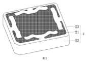
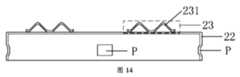
図2は、本願の一実施形態による放熱アセンブリ2の3次元構造の概略図である。図2に示してあるように、放熱アセンブリ2は、要素1に接触するように構成されたヒートスプレッダ21;ヒートスプレッダ21の位置を制限するように構成されたフレームボディ22、ここでフレームボディ22は、ヒートスプレッダ21の側壁を取り囲んでいる;フレームボディ22に固着接続された弾性構造部23、ここで弾性構造部23は、ヒートスプレッダ21のうちの、接触予定の要素1から離れる方に向いた側面に位置している、を含んでよい。2 is a schematic diagram of a three-dimensional structure of a
本願のこの実施形態において提供される放熱アセンブリでは、要素によって生成された熱を均等に伝導できるように、要素に接触するように構成されたヒートスプレッダが配置されており;ヒートスプレッダの位置を制限し、それによりヒートスプレッダが水平方向に移動するのを防止し、ヒートスプレッダの移動に起因した放熱境界面への損傷によって発生する放熱性能への影響を回避できるように、フレームボディが配置されており;さらに、フレームボディに固着接続された弾性構造部が配置されており、弾性構造部は、電子デバイス内の別のコンポーネントに接触し、変形してよく、それにより要素、ヒートスプレッダ、及びフレームボディが、厚さ方向において確実に固定されて、要素によって生成された熱を円滑に伝導できることが確保される。さらに、製造プロセスにおいて、最初に表面実装技術がチップに対して実行されてよく、チップの表面が熱伝導材料でコーティングされ、次いで、放熱アセンブリが取り付けられる。したがって、熱伝導材料の接着強度についての要件が低減し、それにより、より良好な放熱性能を有する熱伝導材料を選択することができる。このように、要素及び放熱アセンブリの間の熱抵抗が小さく、チップの放熱効率がさらに改善される。In the heat dissipation assembly provided in this embodiment of the present application, a heat spreader configured to contact the element is arranged so as to evenly conduct the heat generated by the element; a frame body is arranged so as to limit the position of the heat spreader, thereby preventing the heat spreader from moving in the horizontal direction, and avoiding the impact on the heat dissipation performance caused by damage to the heat dissipation interface due to the movement of the heat spreader; and an elastic structure part fixedly connected to the frame body is arranged, and the elastic structure part may contact and deform with another component in the electronic device, thereby ensuring that the element, the heat spreader, and the frame body are securely fixed in the thickness direction to ensure that the heat generated by the element can be smoothly conducted. Furthermore, in the manufacturing process, a surface mount technology may be performed on the chip first, and the surface of the chip is coated with a thermal conductive material, and then the heat dissipation assembly is attached. Therefore, the requirement for the adhesive strength of the thermal conductive material is reduced, so that a thermal conductive material with better heat dissipation performance can be selected. In this way, the thermal resistance between the element and the heat dissipation assembly is small, and the heat dissipation efficiency of the chip is further improved.
関連技術において、図1を参照されたい。ダイ12及び保護カバー13が、熱伝導材料を介して互いに接合されており、ダイ12によって生成された熱は、熱伝導材料及び保護カバー13を介して伝導される。しかしながら、表面実装技術において、高温リフロープロセスは、高温抵抗性能及び熱伝導材料の接着性が良好であることを必要とするが、良好な接着性を有し、高温抵抗性である熱伝導材料は、概しておよそ2W/mKしかない低い熱伝導係数を有しており、チップの放熱要件を満たすことができない。保護カバー13がダイ12に接合された、図1に示す関連技術の解決策に比べて、放熱アセンブリが配置された本願のこの実施形態では、要素の放熱利得は、7℃~11℃に達することができ、要素の電力消費もある程度まで低減し、それにより要素の性能が改善されることが、実験で証明されている。In the related art, please refer to FIG. 1. The
本願のこの実施形態では、要素がチップである一例を使用して、放熱アセンブリについて説明する。実際の適用例において、放熱アセンブリは、別の要素の熱も放散させてよく、放熱アセンブリの適用シナリオは、実際の要件に基づいて選択されてよい。要素は、本願において限定されない。In this embodiment of the present application, the heat dissipation assembly is described using an example in which the element is a chip. In practical applications, the heat dissipation assembly may also dissipate heat of another element, and the application scenario of the heat dissipation assembly may be selected based on practical requirements. The element is not limited in the present application.
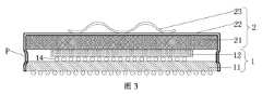
図3は、本願の一実施形態による、要素1の位置における放熱アセンブリの取り付けを示す概略図である。図2及び図3を参照すると、要素1によって生成された熱を伝導するために、ヒートスプレッダ21の一方の面の表面が要素1に接触している。ヒートスプレッダ21の均衡の取れた熱伝導効果を達成するために、ヒートスプレッダ21は、均一な厚さを有するものとして構成されてよい。例えば、ヒートスプレッダ21の厚さは、およそ2mmに設定されてよい。ヒートスプレッダ21の特定の厚さは、要素1の圧力抵抗性及び信頼性に基づき設定されてよい。ヒートスプレッダ21の厚さは、本願において限定されない。弾性構造部23は、ヒートスプレッダ21の、要素1から離れる方に向いた面に位置している。弾性構造部23が変形した後、要素1、ヒートスプレッダ21、及びフレームボディ22は、厚さ方向の定位置に固定されることが可能であり、それにより要素1によって生成された熱は、ヒートスプレッダ21に伝導されることが可能である。加えて、フレームボディ22は、ヒートスプレッダ21の位置を制限し、それによりヒートスプレッダ21が水平方向に移動するのを防止することができる。したがって、放熱アセンブリ2が要素1の位置に取り付けられた後、ヒートスプレッダ21は、水平方向又は厚さ方向に移動しない。これにより、放熱境界面が安定し、それにより要素1によって生成された熱が円滑に伝導されることが確保される。加えて、弾性構造部23は、フレームボディ22のうちの、ヒートスプレッダ21に近い面の縁部に位置していてよい。したがって、ヒートスプレッダ21に対する弾性構造部23の被覆面積は小さく、それによりヒートスプレッダ21の熱伝導性能は影響を受けない。 3 is a schematic diagram showing the installation of a heat dissipation assembly at the position of the
オプションで、本願において図2及び図3に示してあるように、弾性構造部23は、ヒートスプレッダ21に接触してよく、言い換えれば、弾性構造部23は、フレームボディ22の内側に位置している。このように、放熱アセンブリによって占有される空間は小さく、これは、空間の適切な利用にさらに資するものである。もちろん、代替的に、弾性構造部23はヒートスプレッダ21に接触していなくてもよい。例えば、弾性構造部23は、フレームボディ22の外側に位置していてよい。弾性構造部23が変形した後に、要素1、ヒートスプレッダ21、及びフレームボディ22を厚さ方向の位置に固定できる限り、弾性構造部23の特定の位置は、本願において限定されない。Optionally, as shown in FIG. 2 and FIG. 3 in the present application, the
図3を参照されたい。放熱効果をさらに改善するために、ヒートスプレッダ21及び要素1の間の空間が、熱伝導材料で充填されてよい。放熱アセンブリ2は、熱伝導材料の接着強度に対する要件が低いことから、良好な放熱性能能力を有する熱伝導材料を選択することができる。例えば、熱伝導材料は、熱伝導係数がおよそ6W/mKのシリコーン材料であってよく、それにより要素1の放熱効率が改善される。加えて、要素1及びヒートスプレッダ21の間の距離が過度に大きいことによって発生する、要素1からヒートスプレッダ21への熱伝導に対する影響を回避するために、要素1及びヒートスプレッダ21の間の間隙は、0.1mmよりも小さくなるように設定されてよく、例えば0.05mmに設定されてよく、言い換えれば要素1及びヒートスプレッダ21の間に配置される熱伝導材料の厚さは、0.1mmよりも小さい。See FIG. 3. To further improve the heat dissipation effect, the space between the
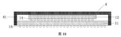
図4は、本願の一実施形態による、光学モジュールへの放熱アセンブリの適用を示す概略図である。図4に示してあるように、光学モジュールは、下部ハウジング31、下部ハウジング31に固着接続された上部カバー32、及びプリント回路基板33を含んでよい。上部カバー32は、放熱ボス34を含む。下部ハウジング31及び上部カバー32は、プリント回路基板33、要素1、及び放熱アセンブリ2を収容できる空間を包囲している。オプションで、下部ハウジング31が、第1のボルトT1を使用することにより上部カバー32に固着接続されてよく、プリント回路基板33は、下部ハウジング31上に配置される。オプションで、プリント回路基板33が、第2のボルトT2を使用することにより下部ハウジング31に固着接続されてよい。もちろん、代替的にプリント回路基板33は、本願において限定しない別の方式で下部ハウジング31に配置されてもよい。要素1は、プリント回路基板33に固定されている。オプションで、要素1は、第1の溶接層15を介してプリント回路基板33に固定されてよい。放熱アセンブリ2は、要素1の位置に取り付けられており、ここで、ヒートスプレッダ21の一方の面の表面は、要素1に接触しており、弾性構造部23は、放熱ボス34に接触している。加えて、弾性構造部23は、特定の範囲まで変形しており、それにより要素1、ヒートスプレッダ21、及びフレームボディ22は、厚さ方向において確実に固定されている。このように、要素1によって生成された熱は、ヒートスプレッダ21及び放熱ボス34を介して均等に伝導されることが可能である。 4 is a schematic diagram showing the application of a heat dissipation assembly to an optical module according to an embodiment of the present application. As shown in FIG. 4, the optical module may include a
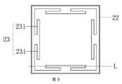
図5は、本願の一実施形態による、放熱アセンブリの構造の概略上面図である。図2及び図5に示してあるように、いくつかの実施形態においては、フレームボディ22の縁部の少なくとも一部分が、ヒートスプレッダ21の表面の縁部の方に曲がっている。このように、フレームボディ22は、垂直方向においてヒートスプレッダ21の位置を制限することができる。加えて、フレームボディ22の縁部は、ヒートスプレッダ21の表面の縁部の方に曲がっていることから、ヒートスプレッダ21に対するフレームボディ22の被覆面積が小さく、それによりヒートスプレッダ21の熱伝導性能は影響を受けない。図6は、破線Lにおける図5の概略断面図である。図6に示してあるように、フレームボディ22はヒートスプレッダ21を取り囲んでおり、フレームボディ22はヒートスプレッダ21に接触しており、それにより水平方向におけるヒートスプレッダ21の位置は制限されることが可能である。5 is a schematic top view of the structure of a heat dissipation assembly according to an embodiment of the present application. As shown in FIG. 2 and FIG. 5, in some embodiments, at least a portion of the edge of the
さらに、本願のこの実施形態に提供される放熱アセンブリにおいては図3を参照されたい。フレームボディ22は、接触予定の要素1の側壁を取り囲み、接触予定の要素1にクランプ留めされるように構成されている。このように、ヒートスプレッダ21は要素1の表面に固定されることが可能であり、それにより要素1、ヒートスプレッダ21、及びフレームボディ22は、水平方向において容易に移動しない。これにより、要素1及びヒートスプレッダ21の間の放熱境界面の安定性がさらに確保される。フレームボディ22及び要素1の間でクランプ留めを実装するために、フレームボディ22は、要素1の側壁の少なくとも一部分に接触してよい。For further heat dissipation assembly provided in this embodiment of the present application, please refer to FIG. 3. The
図3を参照されたい。本願のこの実施形態において、フレームボディ22のうちの、ヒートスプレッダ21からより遠くに離れた面の縁部は、接触予定の要素1の表面と面一になる。このように、フレームボディ22及び要素1の間の接触面積が大きく、それによりフレームボディ22は要素1にさらに容易にクランプ留めされ、ヒートスプレッダ21は、要素1の表面にさらに堅く固定されることが可能である。加えて、フレームボディ22のうちの、ヒートスプレッダ21からより遠く離れた面の縁部は、要素1の、ヒートスプレッダ21から離れる方に向いた面の表面を越えず、それによりフレームボディ22は、要素1の位置にさらに容易に取り付けられることが可能である。さらに、フレームボディ22は、要素1の面積を占有せず、それにより要素1の元の構造を変更する必要がなく、要素1の周りの空間は、フレームボディ22を収容するのに十分である。したがって、本願における放熱アセンブリは、小型の要素1にも適用することができ、それにより、不十分な空間に起因して放熱コンポーネントを小型の要素1に配置できないという関連技術の問題が解決される。 Please refer to Fig. 3. In this embodiment of the present application, the edge ofthe face of the
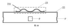
図7は、本願の一実施形態による、放熱アセンブリの構造の別の概略上面図である。図8は、図7に対応した放熱アセンブリの側面図である。図7及び図8に示してあるように、フレームボディ22の側壁には、内部に向かって突出した突出構造部Pが存在している。このように、要素1は、突出構造部Pを使用することによって保持されることが可能であり、それにより、フレームボディ22及び要素1の間のクランプ力がより大きくなり、それによりフレームボディ22、ヒートスプレッダ21、及び要素1が、水平方向において確実に固定されることが確保され、さらに、要素1及びヒートスプレッダ21の間の放熱境界面の安定性が確保される。Figure 7 is another schematic top view of the structure of a heat dissipation assembly according to an embodiment of the present application. Figure 8 is a side view of the heat dissipation assembly corresponding to Figure 7. As shown in Figures 7 and 8, the side wall of the
オプションで、本願のこの実施形態において提供される放熱アセンブリでは、図3に示してあるように、ヒートスプレッダ21のうちの、弾性構造部23から離れる方に向いた側面に、突出構造部Pが位置している。弾性構造部23は、フレームボディ22のうちの、ヒートスプレッダ21の近くにある面の縁部に固定されていることから、ヒートスプレッダ21の位置は、少なくとも弾性構造部23がフレームボディ22に接触する位置に制限されることが可能である。したがって、突出構造部Pは、ヒートスプレッダ21のうちの、弾性構造部23から離れる方に向いた面に配置され、それにより、要素1の位置は、突出構造部Pを使用することによりさらに制限されることが可能であり、それにより、要素1及びヒートスプレッダ21が、水平方向において移動しないことがさらに確保される。加えて、要素1がチップである一例を使用する。要素1は、基板11及びダイ12を含んでよい。ダイ12は、第2の溶接層14を介して基板11に固定されている。概して、ダイ12のサイズは、基板11のサイズよりも小さい。要素1の側壁の位置に突出構造部Pが配置されているので、フレームボディ22は、より容易にクランプ留めされるように要素1に接触することができ、さらに、フレームボディ22及び要素1の間のクランプ力を増大させることができ、それにより要素1はより移動しにくくなる。加えて、代替的に突出構造部Pは、ヒートスプレッダ21に対応した位置に配置されてもよい。突出構造部Pの特定の位置は、本願において限定されない。ダイ12は、ダイであってよく、半導体材料から作られた、パッケージングされていない集積回路本体の小さいブロックであり、集積回路の所与の機能は、半導体のこの小さい部分に実装される。 Optionally, in the heat dissipation assembly provided in this embodiment of the present application, as shown in FIG. 3, a protruding structure P is located on the side of the
図9は、本願の一実施形態による、放熱アセンブリの構造の別の概略上面図である。図10は、図9に対応した放熱アセンブリの側面図である。図9及び図10に示してあるように、突出構造部Pは、フレームボディ22の少なくとも2つの対向する側壁に存在している。例えば、図9に示してある放熱アセンブリでは、フレームボディ22の4つの側壁すべてに突出構造部Pが存在している。図11は、本願の一実施形態による、放熱アセンブリの構造の別の概略上面図である。図12は、図11に対応した放熱アセンブリの側面図である。図11及び図12においては、フレームボディ22の2つの対向する側壁に突出構造部Pが存在している。このように、フレームボディ22のクランプ力をより均等にすることができ、それにより、フレームボディ22の不均等なクランプ力によって発生する要素1及びヒートスプレッダ21の間の相対的な移動が回避される。9 is another schematic top view of the structure of the heat dissipation assembly according to an embodiment of the present application. FIG. 10 is a side view of the heat dissipation assembly corresponding to FIG. 9. As shown in FIG. 9 and FIG. 10, the protruding structure P is present on at least two opposing side walls of the
オプションで、本願の実施形態では、フレームボディ22の少なくとも1つの側壁のそれぞれに、1つ又は複数の突出構造部Pが存在している。図13は、本願の一実施形態による放熱アセンブリの構造の別の概略上面図である。図14は、図13に対応した放熱アセンブリの側面図である。図13及び図14に示してあるように、フレームボディ22の少なくとも1つの側壁のそれぞれに、1つの突出構造部Pが存在してよい。図15は、本願の一実施形態による、放熱アセンブリの構造の別の概略上面図である。図16は、図15に対応した放熱アセンブリの側面図である。図15及び図16に示してあるように、代替的には、フレームボディ22の少なくとも1つの側壁のそれぞれに、複数の突出構造部Pが存在してよい。このように、フレームボディ22のクランプ力を増大させることができ、それによりヒートスプレッダ21及び要素1に対するフレームボディ22のクランプ留めのより良好な効果が達成され、それによりヒートスプレッダ21及び要素1が、より移動しにくくなる。図15及び図16においては、フレームボディ22の1つの側壁に3つの突出構造部Pが存在する一例を、図解のために使用しており、突出構造部Pの数量は限定されない。加えて、図7~図16においては、フレームボディ22の側壁の中央区域の近くに突出構造部Pがある一例を、図解のために使用している。実際の適用例では、突出構造部Pの位置は、実際の要件に基づき設定されてよい。突出構造部Pの位置は、本願において限定されない。Optionally, in an embodiment of the present application, one or more protruding structures P are present on each of at least one side wall of the
本願のすべての添付図面において、限定された数量の突出構造部P及び弾性構造部23が、図解のための一例として使用されているが、これは、突出構造部P及び弾性構造部23の数量に限定を課すものではない。加えて、本願のすべての添付図面において、突出構造部Pが正方形である一例を、図解のために使用している。実際の適用例では、代替的に突出構造部Pは、円形、台形、又は別の形状として構成されてもよい。突出構造部Pの形状は、本願において限定されない。In all the accompanying drawings of this application, a limited number of protruding structures P and
オプションで、本願の実施形態における放熱アセンブリにおいては、図5に示してあるように、弾性構造部23が、フレームボディ22の少なくとも2つの対向する縁部に配置されている。このように、弾性構造部23が圧縮下で変形した後、ヒートスプレッダ21及び要素1に加えられる弾性力がより均等になり、それにより、ヒートスプレッダ21及び要素1に加えられる不均等な弾性力によって発生する相対的な移動が回避される。例えば、図5及び図6では、弾性構造部23は、フレームボディ22のすべての面の縁部に配置されている;図9及び図10に示してあるように、弾性構造部23は、フレームボディ22の2つの対向する面の縁部に配置されている。 Optionally, in the heat dissipation assembly in the embodiment of the present application, the
本願の一実施形態において、図5及び図6に示してあるように、弾性構造部23はばねプレートである。In one embodiment of the present application, as shown in Figures 5 and 6, the
弾性構造部23は、少なくとも1つの突出部分231を有する。突出部分231は、ヒートスプレッダ21から離れる方に向いて突出している。The
弾性構造部23は、ばねプレートとして構成されており、少なくとも1つの突出部分231が提供されており、それにより、圧縮下で弾性構造部23が変形したとき、弾性力が生成されることが可能であり、ヒートスプレッダ21及び要素1は、互いに密着することができる。加えて、突出部分231の一方の端部は固定されてよく、その一方で他方の端部は可動であり、それにより、突出部分231が圧縮されたとき、可動端部は、ヒートスプレッダ21の表面上を摺動することができ、突出部分231が圧縮されていないときには、可動端部は、初期状態に戻ることができる。このように、弾性構造部23の弾性能力が強力になる。The
オプションで、本願の実施形態における放熱アセンブリにおいて、図6に示してあるように、突出部分231は円弧形状であってよい。このように、弾性構造部23は、より容易に変形することができ、弾性構造部23の弾性が良好になる。Optionally, in the heat dissipation assembly in the embodiment of the present application, as shown in FIG. 6, the protruding
いくつかの実施形態において、本願の実施形態において提供される放熱アセンブリでは、図5に示してあるように、対称的に配置された2つの突出部分231を弾性構造部23が有しており、それにより弾性構造部23の弾性能力が増大する。2つの突出部分231の固定端部は、2つの突出部分231の他方の端部がなお可動であるように接続されてよい。例えば、弾性構造部23は、弾性構造部23の弾性が良好になるように、一体構造部として構成されてよい。図11及び図12に示してあるように、代替的に弾性構造部23は、1つの突出部分231を有してもよい。図12は図11の側面図であることから、図12では2つの突出部分231が存在しているが、これら2つの突出部分231は、同じ弾性構造部に属していないことに留意されたい。もちろん、代替的に弾性構造部23は、より多くの突出部分231を有してもよい。弾性構造部23における突出部分231の数量は、本願において限定されない。In some embodiments, in the heat dissipation assembly provided in the embodiment of the present application, as shown in FIG. 5, the
オプションで、本願の実施形態における放熱アセンブリでは、図5に示してあるように、突出部分231はストリップ形状であってよい。Optionally, in the heat dissipation assembly of the present embodiment, the protruding
図5及び図6に示してあるように、突出部分231の延伸方向は、ヒートスプレッダ21の縁部の延伸方向と同じである。代替的に、図13及び図14に示してあるように、突出部分231の延伸方向及びヒートスプレッダ21の縁部の延伸方向の間に、特定の挟角が存在している。突出部分231が、これら2つの方式のうちのいずれかで配置されたとき、ヒートスプレッダのうちの、突出部分231によって占有される面積が小さくなり、それにより要素の放熱効果は影響を受けない。実際の適用例においては、要素の熱をより効果的に放散するために、突出部分231の延伸方向は、要素の特定の構造に基づき設定されてよい。5 and 6, the extension direction of the protruding
本願のいくつかの実施形態において、弾性構造部の材料は、弾性のプラスチック材料又は金属材料を含んでよい。弾性構造部が、弾性のプラスチック材料又は金属材料から作られたとき、弾性構造部は良好な弾性を有することができる。例えば、弾性構造部は、弾性の薄鋼板又は板金部品として製造されてよい。もちろん、代替的に弾性構造部は、別の弾性材料から作られてもよい。例えば、代替的に弾性構造部は、プラスチック材料から作られてもよい。これは、本願において限定されるものではない。In some embodiments of the present application, the material of the elastic structure may include an elastic plastic material or a metal material. When the elastic structure is made of an elastic plastic material or a metal material, the elastic structure may have good elasticity. For example, the elastic structure may be manufactured as an elastic thin steel plate or sheet metal part. Of course, the elastic structure may alternatively be made of another elastic material. For example, the elastic structure may alternatively be made of a plastic material. This is not a limitation in the present application.
オプションで、本願の実施形態において提供される放熱アセンブリでは、図3に示してあるように、ヒートスプレッダ21の形状は、接触予定の要素1の輪郭の形状と同じであり、ヒートスプレッダ21のサイズは、要素1の輪郭のサイズと同じである。Optionally, in the heat dissipation assembly provided in the embodiments of the present application, the shape of the
本願における要素1の輪郭は、要素1の最も外側の縁部によって包囲された形状として理解されてよいことに留意されたい。要素1がチップである一例を使用する。要素1内の基板11のサイズは、ダイ12のサイズよりも大きく、したがって、要素1の輪郭は、基板11の輪郭であってよい。Please note that the outline of
ヒートスプレッダ21の形状及びサイズは、要素1の輪郭の形状及びサイズと同じになるように設定されている。このように、ヒートスプレッダ21の熱放散面積を大きくすることができ、それにより要素1の放熱効率が改善される。加えて、これにより、ヒートスプレッダ21の位置をフレームボディ22が制限しやすくなり、フレームボディ22及び要素1の間でより良好なクランプ留め効果も達成され、それによりヒートスプレッダ21及び要素1は、容易に移動せず、それによりヒートスプレッダ21及び要素1の間の放熱境界面の安定性が確保される。The shape and size of the
いくつかの実施形態において、本願の実施形態で提供される放熱アセンブリでは、ヒートスプレッダの材料が金属材料を含んでよい。金属材料は、強力な熱伝導能力を有する。ヒートスプレッダが金属材料から作られたとき、要素の熱は迅速に伝導されることが可能であり、それにより要素の放熱効率が改善される。例えば、ヒートスプレッダは、銅、鉄、又はアルミニウムなど、高い熱伝導率を有する材料から作られてよい。もちろん、代替的にヒートスプレッダは、強力な熱伝導能力を有する別の材料から作られてもよい。ヒートスプレッダの材料は、本願において限定されない。本願の実施形態においては、ヒートスプレッダ及び要素の間の間隙が小さく、例えば0.1mmよりも小さくなるように設定されてよく、ヒートスプレッダの熱伝導能力が強力であり、例えばヒートスプレッダが銅から作られたとき、ヒートスプレッダの熱伝導性は400W/mKに達することができるので、要素によって生成される熱は、均等且つ迅速に伝導されることが可能である。In some embodiments, in the heat dissipation assembly provided in the embodiments of the present application, the material of the heat spreader may include a metal material. The metal material has a strong thermal conduction ability. When the heat spreader is made of a metal material, the heat of the element can be rapidly conducted, thereby improving the heat dissipation efficiency of the element. For example, the heat spreader may be made of a material with high thermal conductivity, such as copper, iron, or aluminum. Of course, alternatively, the heat spreader may be made of another material with strong thermal conduction ability. The material of the heat spreader is not limited in the present application. In the embodiments of the present application, the gap between the heat spreader and the element may be set to be small, for example, smaller than 0.1 mm, and the heat spreader has a strong thermal conduction ability, for example, when the heat spreader is made of copper, the thermal conductivity of the heat spreader can reach 400 W/mK, so that the heat generated by the element can be conducted evenly and quickly.
オプションで、本願の実施形態において図3を参照されたい。フレームボディ22及び弾性構造部23は、一体構造であってよい。このように、弾性構造部23及びフレームボディ22は、より堅く接続されることが可能である。さらに、製造中に、フレームボディ22及び弾性構造部23は、同じプロセスを介して直接形成されることが可能であり、それにより製造段階が減少し、製造コストが削減される。もちろん、代替的に弾性構造部23及びフレームボディ22は、2つの別個のコンポーネントであってよく、その場合、弾性構造部23は、溶接又は接合などの方式でフレームボディ22の縁部の位置に固定される。フレームボディ22及び弾性構造部23を配置する特定の方式は、本願において限定されない。Optionally, see FIG. 3 in the embodiment of the present application. The
いくつかの実施形態において、本願の実施形態で提供される放熱アセンブリでは、フレームボディは取り外し可能な構造である。製造プロセスにおいて、チップに対して最初に表面実装技術が実行されてよく、次いで、チップの表面が熱伝導材料でコーティングされ、次いで、放熱アセンブリが取り付けられる。したがって、熱伝導材料の接着強度についての要件が低減し、それにより、より良好な放熱性能を有する熱伝導材料を選択することができ、それによりチップの放熱効率がさらに改善される。加えて、フレームボディが取り外し可能な構造として配置されたとき、フレームボディ、ヒートスプレッダ、及び要素を固定する方式が簡単になる。In some embodiments, in the heat dissipation assembly provided in the embodiments of the present application, the frame body is a removable structure. In the manufacturing process, the surface mount technology may be performed on the chip first, then the surface of the chip is coated with a thermal conductive material, and then the heat dissipation assembly is attached. Therefore, the requirement for the adhesive strength of the thermal conductive material is reduced, so that a thermal conductive material with better heat dissipation performance can be selected, which further improves the heat dissipation efficiency of the chip. In addition, when the frame body is arranged as a removable structure, the manner of fixing the frame body, the heat spreader, and the elements is simplified.
同じ技術的概念に基づき、本願の一実施形態はさらに、電子デバイスを提供する。図17に示してあるように、電子デバイスは、上で説明した要素1及び任意の放熱アセンブリ2を含む。要素1は、放熱アセンブリ2内のヒートスプレッダに接触している。本願のこの実施形態で提供される電子デバイスにおいて、放熱アセンブリは、要素の位置に取り付けられており、それにより、要素によって生成された熱は、放熱アセンブリを介して伝導されることが可能であり、それにより電子デバイスの放熱効率が改善される。要素は、電子的要素、光学的要素、光電子的要素などを含むが、これらに限定されない。Based on the same technical concept, an embodiment of the present application further provides an electronic device. As shown in FIG. 17, the electronic device includes the above-described
図17では、電子デバイスが光学モジュールである一例を、図解のために使用している。光学モジュールは、光から電気への変換及び電気から光への変換を実装するコンポーネントであり、光通信デバイスの重要な機能的モジュールである。図17に示してあるように、電子デバイスはさらに、光学コンポーネント35を含んでよい。本願においては、電子デバイスが光学モジュールである例を、説明のために使用している。もちろん、代替的に電子デバイスは、放熱を必要とする別のデバイスであってよく、放熱アセンブリは、電子デバイス内で放熱を必要とする要素の位置に取り付けられさえすればよい。電子デバイスのタイプは、本願において限定されない。17, an example in which the electronic device is an optical module is used for illustration. The optical module is a component that implements optical to electrical conversion and electrical to optical conversion, and is an important functional module of an optical communication device. As shown in FIG. 17, the electronic device may further include an optical component 35. In this application, an example in which the electronic device is an optical module is used for explanation. Of course, the electronic device may alternatively be another device that requires heat dissipation, and the heat dissipation assembly only needs to be attached to the position of the element that requires heat dissipation in the electronic device. The type of electronic device is not limited in this application.
本願のこの実施形態においては、図4を参照されたい。電子デバイスは、下部ハウジング31、下部ハウジング31に固着接続された上部カバー32、及びプリント回路基板33をさらに含んでよい。プリント回路基板33は、下部ハウジング31に配置されている。要素1は、プリント回路基板33のうちの、下部ハウジング31から離れる方に向いた面に固定されている。下部ハウジング31に近い上部カバー32の面に、放熱ボス34が配置されている。放熱アセンブリ2の弾性構造部23が、放熱ボス34に接触しており、弾性構造部23は変形している。 In this embodiment of the present application, please refer to Fig. 4. The electronic device may further include a
下部ハウジング31及び上部カバー32は、プリント回路基板33、要素1、及び放熱アセンブリ2を収容することができる空間を包囲している。オプションで、下部ハウジング31は、第1のボルトT1を使用することにより、上部カバー32に固着接続されてよく、プリント回路基板33は、第2のボルトT2を使用することにより、下部ハウジング31に固着接続されてよい。代替的に、プリント回路基板33は、本願において限定されない別の方式で、下部ハウジング31に配置されてもよい。要素1は、プリント回路基板33に固定されている。オプションで、要素1は、第1の溶接層15を介してプリント回路基板33に固定されてよい。放熱アセンブリ2は、要素1の位置に取り付けられ、この位置において、ヒートスプレッダ21の一方の面の表面が要素1に接触し、ヒートスプレッダの他方の面の表面が弾性構造部23に接触し、弾性構造部23が放熱ボス34に接触している。加えて、弾性構造部23は、特定の範囲まで変形しており、それにより要素1、ヒートスプレッダ21、及びフレームボディ22は、厚さ方向において確実に固定されている。このように、要素1によって生成された熱は、ヒートスプレッダ21及び放熱ボス34を介して均等に伝導されることが可能である。 The
いくつかの実施形態において、本願のこの実施形態で提供される電子デバイスでは、図4を参照されたい。放熱ボス34及びヒートスプレッダ21の間の空間には、第1の熱伝導材料(図示せず)が充填されている。例えば、第1の熱伝導材料は、サーマルゲルであってよい。弾性構造部23及び第1の熱伝導材料のための十分な空間を取るために、放熱ボス34及びヒートスプレッダ21の間の間隙は、0.5mmよりも小さくなるように設定されてよい。加えて、第1の熱伝導材料は軟質材料であり、弾性構造部23が圧縮及び伸長したとき、第1の熱伝導材料は、弾性構造部23とともに流れることができ、それにより、弾性構造部23の弾性能力に第1の熱伝導材料が影響を及ぼすことが防止される。In some embodiments, in the electronic device provided in this embodiment of the present application, see FIG. 4. The space between the
オプションで、本願のこの実施形態で提供される電子デバイスにおいては、図4を参照されたい。ヒートスプレッダ21は、第2の熱伝導材料(図示せず)を介して要素1に接触している。放熱アセンブリ2は、熱伝導材料の接着強度に対する要件が低いことから、良好な放熱能力を有する熱伝導材料を、第2の熱伝導材料として選択することができる。例えば、第2の熱伝導材料の材料は、熱伝導係数がおよそ6W/mKであるシリコーン材料を含んでよく、それにより要素1の放熱効率が改善される。加えて、代替的に第2の熱伝導材料の材料は、高い熱伝導率を有する別の材料であってもよい。これは、本願において限定されるものではない。加えて、要素1及びヒートスプレッダ21の間の距離が過度に大きいことによって発生する、要素1からヒートスプレッダ21への熱伝導に対する影響を回避するために、要素1及びヒートスプレッダ21の間の間隙は、0.1mmよりも小さくなるように設定されてよく、例えば0.05mmに設定されてよく、つまり要素1及びヒートスプレッダ21の間に配置される熱伝導材料の厚さは、0.1mmよりも小さい。Optionally, in the electronic device provided in this embodiment of the present application, see FIG. 4. The
図1に示してある関連技術において、チップは概して、基板11、基板11に固定されたダイ12、及び保護カバー13を含んでよい。保護カバー13は、熱伝導材料を使用することによりダイ12に接合されている。加えて、保護カバー13は、チップの4つの角部又は周囲に接合されており、したがって、保護カバー13は、チップパッケージのレイアウト面積を占有している。In the related art shown in FIG. 1, a chip may generally include a
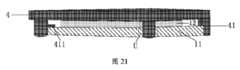
これに基づき、チップパッケージのレイアウト面積を保護カバーが占有するという問題を解決するために、本願の一実施形態は、チップパッケージ構造を提供する。
図18は、本願の一実施形態による、チップパッケージ構造の側面図である。図18に示してあるように、チップパッケージ構造は、基板11、基板11に固定されたダイ12、及びカバープレート4を含んでよい。ダイ12の縁部は、基板11の縁部の範囲内に位置している。オプションで、ダイ12は、第2の溶接層14を介して基板11に固定されてよい。
図19は、本願の一実施形態による、チップパッケージ構造の構造の概略平面図である。パッケージングのための十分な空間を取るために、ダイ12の縁部が、基板11の縁部の範囲内に位置しており、つまりダイ12のサイズが、基板11のサイズよりも小さいことを、図19から明確に確認することができる。ダイは、ダイであってよく、半導体材料から作られた、パッケージングされていない集積回路本体の小さいブロックであり、集積回路の所与の機能は、半導体のこの小さい部分に実装される。 Based on this, to solve the problem of the protective cover occupying the layout area of the chip package, an embodiment of the present application provides a chip package structure.
18 is a side view of a chip package structure according to an embodiment of the present application. As shown in FIG. 18, the chip package structure may include a
19 is a schematic plan view of the structure of a chip package structure according to an embodiment of the present application. It can be clearly seen from FIG. 19 that the edge of the die 12 is located within the edge of the
図20及び図21は、本願の一実施形態による、チップパッケージ構造の3次元構造の別の概略図である。
図20及び図21を一緒に参照されたい。ダイ12のうちの、基板11から離れる方に向いた面に、カバープレート4が位置しており;カバープレート4は、基板11に近い面に支柱41を有しており、この支柱41は、カバープレート4の縁部に固定されており;基板11には、支柱41に対応した位置にノッチUが提供されており;支柱41は、ノッチUの内面を介して基板11に固着接続されている。オプションで、ノッチUは、基板11の4つの角部又は側面縁部に配置されてよい。これは、本願において限定されるものではない。ノッチUは、四半円の穴又は半円の穴であってもよいし、又は別の形状であってもよく、これは本願において限定されない。 20 and 21 are another schematic diagrams of a three-dimensional structure of a chip package structure according to one embodiment of the present application.
Please refer to Figures 20 and 21 together. A cover plate 4 is located onthe surface of the die 12 facing away from the
本願のこの実施形態で提供されるチップパッケージ構造では、支柱を有するカバープレートが配置されており、カバープレートには、支柱に対応した位置にノッチが提供されており、支柱は、ノッチの内面を介して基板に固着接続されている。したがって、カバープレートは、要素の面積を占有せず、要素パッケージのレイアウト面積が増大する。本願のカバープレートでは、要素のレイアウト面積をおよそ9%増やせることが、実験により証明されている。In the chip package structure provided in this embodiment of the present application, a cover plate having support posts is disposed, and notches are provided in the cover plate at positions corresponding to the support posts, and the support posts are fixedly connected to the substrate via the inner surface of the notch. Thus, the cover plate does not occupy the area of the element, and the layout area of the element package is increased. It has been experimentally proven that the cover plate of the present application can increase the layout area of the element by approximately 9%.
本願のこの実施形態では、図18に示してあるように、支柱41のうちの、カバープレート4から離れる方に向いた面の表面が、基板11のうちの、カバープレート4から離れる方に向いた面の表面と面一になる。このように、過度に大きい間隙に起因して要素1及びカバープレート4の間の熱抵抗が増大する事例を回避し、過度に小さい間隙に起因して要素1が圧搾される事例を回避するために、ダイ12及びカバープレート4の間の間隙は、支柱41を使用することによって制御されることが可能である。 In this embodiment of the present application, thesurface of the support posts 41 facing away from the cover plate 4 is flush with the surface of the
オプションで、図21を参照されたい。支柱41に対応したノッチUを形成するために、基板11上の、支柱41に対応した位置がフライス加工されてよく、支柱41は、接合材料を使用することにより、ノッチUの内面に固定される。オプションで、基板11のノッチUの内面は、金属層を有してよい。例えば、基板11のノッチUに、銅めっきが配置されてよい。したがって、支柱41は、金属層を介してノッチUの内面に溶接されてよく、それにより支柱41及び基板11の間の接続がより堅くなる。もちろん、代替的に別の接合材料を使用して、支柱41がノッチUの内面に固定されてもよい。例えば、強い接着力を有する接着剤が使用されてよい。接合材料は、本願において限定されない。Optionally, see FIG. 21. To form a notch U corresponding to the
さらに、本願のこの実施形態において提供されるチップパッケージ構造では、支柱41は、図21に示してあるように、内部に向かって突出した固定部分411を有しており、この固定部分411が、カバープレート4に近い基板11の面の表面に接触している。支柱41には、固定部分411が提供されており、固定部分411は、基板11の表面に接触しており、それにより支柱41の支持能力がさらに強化されることが可能であり、それによりダイ12及びカバープレート4の間で特定の間隙を保持することが確保される。加えて、本願のこの実施形態において、図18を参照されたい。ダイ12及びカバープレート4の間の空間には、第3の熱伝導材料(図示せず)が充填されてよい。ダイ12によって生成された熱は、第3の熱伝導材料を介して伝導され、それによりチップパッケージ構造の放熱効率が改善される。 Furthermore, in the chip package structure provided in this embodiment of the present application, the
前述の説明は、本願の具体的な実装例に過ぎず、本願の保護範囲を限定することを意図するものではない。本願で開示された技術的範囲内で当業者が容易に想到する任意の変形又は置換は、本願の保護範囲に含まれるものとする。したがって、本願の保護範囲は、特許請求の範囲の保護範囲に従うものとする。
(他の可能な項目)
(項目1)
要素の放熱アセンブリであって、
前記要素(1)に接触するように構成されたヒートスプレッダ(21);
前記ヒートスプレッダ(21)の位置を制限するように構成されたフレームボディ(22)、ここで前記フレームボディ(22)は、前記ヒートスプレッダ(21)の側壁を取り囲んでいる;及び
前記フレームボディ(22)に固着接続された弾性構造部(23)、ここで前記弾性構造部(23)は、接触予定の前記要素(1)から離れる方に向いた前記ヒートスプレッダ(21)の面に位置している
を備える、放熱アセンブリ。
(項目2)
前記フレームボディ(22)の縁部の少なくとも一部分が、前記ヒートスプレッダ(21)の表面の縁部の方に曲がっている、項目1に記載の放熱アセンブリ。
(項目3)
前記フレームボディ(22)が、接触予定の前記要素(1)の側壁を取り囲み、接触予定の前記要素(1)にクランプ留めされるように構成されている、項目1に記載の放熱アセンブリ。
(項目4)
前記ヒートスプレッダ(21)からより遠く離れた、前記フレームボディ(22)の面の縁部が、接触予定の前記要素(1)の表面と面一になる、項目3に記載の放熱アセンブリ。
(項目5)
前記フレームボディ(22)の側壁に、内部に向かって突出した突出構造部(P)が存在している、項目3に記載の放熱アセンブリ。
(項目6)
前記突出構造部(P)が、前記弾性構造部(23)から離れる方に向いた前記ヒートスプレッダ(21)の面に位置している、項目5に記載の放熱アセンブリ。
(項目7)
前記フレームボディ(22)の少なくとも2つの対向する側壁に、突出構造部(P)が存在している、項目5に記載の放熱アセンブリ。
(項目8)
前記フレームボディ(22)の少なくとも1つの側壁のそれぞれに、1つ又は複数の突出構造部(P)が存在している、項目5に記載の放熱アセンブリ。
(項目9)
前記フレームボディ(22)の少なくとも2つの対向する縁部に、弾性構造部(23)が配置されている、項目1に記載の放熱アセンブリ。
(項目10)
前記弾性構造部(23)がばねプレートであり;
前記弾性構造部(23)が少なくとも1つの突出部分(231)を有し、前記突出部分(231)が、前記ヒートスプレッダ(21)から離れる方に向いて突出している、項目1から9のいずれか1項に記載の放熱アセンブリ。
(項目11)
前記突出部分(231)が円弧形状である、項目10に記載の放熱アセンブリ。
(項目12)
前記弾性構造部(23)が、対称に配置された2つの突出部分(231)を有する、項目10に記載の放熱アセンブリ。
(項目13)
前記突出部分(231)がストリップ形状であり;
前記突出部分(231)の延伸方向が、前記ヒートスプレッダ(21)の縁部の延伸方向と同じであるか;又は
前記突出部分(231)の延伸方向及び前記ヒートスプレッダ(21)の縁部の延伸方向の間に特定の挟角が存在している、項目10に記載の放熱アセンブリ。
(項目14)
前記弾性構造部(23)の材料が、弾性のプラスチック材料又は金属材料を含む、項目1に記載の放熱アセンブリ。
(項目15)
前記ヒートスプレッダ(21)の形状が、接触予定の前記要素(1)の輪郭の形状と同じであり;
前記ヒートスプレッダ(21)のサイズが、前記要素(1)の前記輪郭のサイズと同じである、項目1に記載の放熱アセンブリ。
(項目16)
前記ヒートスプレッダ(21)の材料が、金属材料を含む、項目1に記載の放熱アセンブリ。
(項目17)
前記フレームボディ(22)及び前記弾性構造部(23)が一体構造である、項目1から16のいずれか1項に記載の放熱アセンブリ。
(項目18)
前記フレームボディ(22)が取り外し可能な構造である、項目1から16のいずれか1項に記載の放熱アセンブリ。
(項目19)
要素(1)及び項目1から18のいずれか1項に記載の放熱アセンブリ(2)を備える電子デバイスであって、前記要素(1)が、前記放熱アセンブリ(2)内のヒートスプレッダに接触している、電子デバイス。
(項目20)
下部ハウジング(31)、前記下部ハウジング(31)に固着接続された上部カバー(32)、及びプリント回路基板(33)をさらに備え、
前記プリント回路基板(33)が、前記下部ハウジング(31)に配置されており、前記要素(1)が、前記プリント回路基板(33)のうちの、前記下部ハウジング(31)から離れる方に向いた面に固定されており;
前記下部ハウジング(31)に近い前記上部カバー(32)の面に、放熱ボス(34)が配置されており、前記放熱アセンブリ(2)の弾性構造部(23)が、前記放熱ボス(34)に接触しており、前記弾性構造部(23)が変形している、項目19に記載の電子デバイス。
(項目21)
前記放熱ボス(34)及び前記ヒートスプレッダ(21)の間の空間に、第1の熱伝導材料が充填されている、項目20に記載の電子デバイス。
(項目22)
前記ヒートスプレッダ(21)が、第2の熱伝導材料を介して前記要素(1)に接触している、項目19から21のいずれか1項に記載の電子デバイス。
(項目23)
前記第2の熱伝導材料の材料が、シリコーン材料を含む、項目22に記載の電子デバイス。
(項目24)
基板(11)、前記基板(11)に固定されたベアダイ(12)、及びカバープレート(4)を備え、
前記ベアダイ(12)の縁部が、前記基板(11)の縁部の範囲内に位置しており;
前記カバープレート(4)が、前記ベアダイ(12)のうちの、前記基板(11)から離れる方に向いた面に位置しており;
前記カバープレート(4)が、前記基板(11)に近い面に支柱(41)を有し、前記支柱(41)が、前記カバープレート(4)の縁部に固定されており;
前記基板(11)には、前記支柱(41)に対応した位置にノッチ(U)が提供されており、前記支柱(41)が、前記ノッチ(U)の内面を介して、前記基板(11)に固着接続されている
チップパッケージ構造。
(項目25)
前記支柱(41)のうちの、前記カバープレート(4)から離れる方に向いた面の表面が、前記基板(11)のうちの、前記カバープレート(4)から離れる方に向いた面の表面と面一になっている、項目24に記載のチップパッケージ構造。
(項目26)
前記基板(11)の前記ノッチ(U)の前記内面が、金属層を有する、項目24に記載のチップパッケージ構造。
(項目27)
前記支柱(41)が、内部に向かって突出した固定部分(411)を有し;
前記固定部分(411)が、前記カバープレート(4)に近い前記基板(11)の面の表面に接触している、項目24から26のいずれか1項に記載のチップパッケージ構造。
(項目28)
前記ベアダイ(12)及び前記カバープレート(4)の間の空間に、第3の熱伝導材料が充填されている、項目24から26のいずれか1項に記載のチップパッケージ構造。 The above description is merely a specific implementation example of the present application, and is not intended to limit the scope of protection of the present application. Any modifications or replacements that are easily conceived by those skilled in the art within the technical scope disclosed in the present application shall be included in the scope of protection of the present application. Therefore, the scope of protection of the present application shall be subject to the scope of protection of the claims.
(Other possible items)
(Item 1)
A heat dissipation assembly of an element, comprising:
A heat spreader (21) configured to contact said element (1);
a frame body (22) configured to limit the position of the heat spreader (21), wherein the frame body (22) surrounds a side wall of the heat spreader (21); and a resilient structure (23) fixedly connected to the frame body (22), wherein the resilient structure (23) is located ona surface of the heat spreader (21) facing away from the element (1) with which it is to come into contact.
(Item 2)
2. The heat dissipation assembly of
(Item 3)
2. The heat dissipation assembly according to
(Item 4)
4. The heat dissipation assembly according to claim 3, wherein an edge ofa face of the frame body (22) farther away from the heat spreader (21) is flush with a surface of the element (1) with which it is to come into contact.
(Item 5)
4. The heat dissipation assembly according to claim 3, wherein a protruding structure (P) protruding inwardly is present on a side wall of the frame body (22).
(Item 6)
6. The heat dissipation assembly according to claim 5, wherein the protruding structure (P) is located ona surface of the heat spreader (21) facing away from the elastic structure (23).
(Item 7)
6. The heat dissipation assembly according to claim 5, wherein a protruding structure (P) is present on at least two opposing side walls of the frame body (22).
(Item 8)
6. The heat dissipation assembly according to claim 5, wherein one or more protruding structures (P) are present on each of at least one sidewall of the frame body (22).
(Item 9)
2. The heat dissipation assembly according to
(Item 10)
The elastic structure (23) is a spring plate;
10. The heat dissipation assembly of any one of
(Item 11)
(Item 12)
(Item 13)
said protruding portion (231) being strip-shaped;
(Item 14)
(Item 15)
The shape of the heat spreader (21) is the same as the contour shape of the element (1) that it is to contact;
2. The heat dissipation assembly of
(Item 16)
(Item 17)
17. The heat dissipation assembly according to any one of the preceding claims, wherein the frame body (22) and the elastic structure (23) are of one piece construction.
(Item 18)
17. The heat dissipation assembly according to any one of the preceding claims, wherein the frame body (22) is a removable structure.
(Item 19)
19. An electronic device comprising an element (1) and a heat dissipation assembly (2) according to any one of
(Item 20)
The device further comprises a lower housing (31), an upper cover (32) fixedly connected to the lower housing (31), and a printed circuit board (33),
the printed circuit board (33) is disposed in the lower housing (31), and the element (1) is fixed to asurface of the printed circuit board (33) facing away from the lower housing (31);
20. The electronic device according to claim 19, wherein a heat dissipation boss (34) is disposed ona surface of the upper cover (32) close to the lower housing (31), and an elastic structure (23) of the heat dissipation assembly (2) is in contact with the heat dissipation boss (34), and the elastic structure (23) is deformed.
(Item 21)
(Item 22)
22. The electronic device of any one of claims 19 to 21, wherein the heat spreader (21) is in contact with the element (1) via a second thermally conductive material.
(Item 23)
23. The electronic device of
(Item 24)
The device comprises a substrate (11), a bare die (12) fixed to the substrate (11), and a cover plate (4),
The edge of the bare die (12) is located within the edge of the substrate (11);
The cover plate (4) is located on asurface of the bare die (12) facing away from the substrate (11);
The cover plate (4) has a support (41) ona surface close to the substrate (11), and the support (41) is fixed to an edge of the cover plate (4);
The substrate (11) is provided with a notch (U) at a position corresponding to the support (41), and the support (41) is fixedly connected to the substrate (11) through the inner surface of the notch (U).
(Item 25)
25. The chip package structure according to item 24, wherein thesurface of the support (41) facing away from the cover plate (4) isflush with the surface of the substrate (11) facing away from the cover plate (4).
(Item 26)
25. The chip package structure according to item 24, wherein the inner surface of the notch (U) of the substrate (11) has a metal layer.
(Item 27)
The support (41) has a fixing portion (411) protruding inwardly;
27. The chip package structure according to any one of items 24 to 26, wherein the fixing portion (411) is in contact with a surface of aside of the substrate (11) that is closer to the cover plate (4).
(Item 28)
27. The chip package structure of any one of items 24 to 26, wherein a space between the bare die (12) and the cover plate (4) is filled with a third thermally conductive material.
Claims (24)
Translated fromJapanese前記要素に接触するように構成されたヒートスプレッダ;
前記ヒートスプレッダの位置を制限するように構成されたフレームボディ、ここで前記フレームボディは、前記ヒートスプレッダの側壁を取り囲んでいる;及び
前記フレームボディに固着接続された弾性構造部、ここで前記弾性構造部は、前記ヒートスプレッダのうちの、接触予定の前記要素から離れる方に向いた面に位置し、前記弾性構造部は、前記フレームボディに接続される接続部分と、前記接続部分に対して対称的に配置され、前記接続部分よりも前記ヒートスプレッダから離れる方向に突出する2つの突出部分を有する、
を備える、放熱アセンブリ。 A heat dissipation assembly of an element, comprising:
a heat spreader configured to contact the element;
a frame body configured to limit the position of the heat spreader, the frame body surrounding a side wall of the heat spreader; and a resilient structure fixedly connected to the frame body, the resilient structure being located on a surface of the heat spreader facing away from the element to be contacted, the resilient structure havinga connection portion connected to the frame body and two protruding portions disposed symmetrically with respect to the connection portion and protruding in a direction away from the heat spreader beyond the connection portion.
A heat dissipation assembly comprising:
前記放熱アセンブリが、
前記要素に接触するように構成されたヒートスプレッダ;
前記ヒートスプレッダの位置を制限するように構成されたフレームボディ、ここで前記フレームボディは、前記ヒートスプレッダの側壁を取り囲んでいる;及び
前記フレームボディに固着接続された弾性構造部、ここで前記弾性構造部は、前記ヒートスプレッダのうちの、接触予定の前記要素から離れる方に向いた面に位置し、前記弾性構造部は、前記フレームボディに接続される接続部分と、前記接続部分に対して対称的に配置され、前記接続部分よりも前記ヒートスプレッダから離れる方向に突出する2つの突出部分を有する、
を有し、
前記要素が前記放熱アセンブリ内の前記ヒートスプレッダに接触している、電子デバイス。 An electronic device comprising a component and a heat dissipation assembly,
The heat dissipation assembly comprises:
a heat spreader configured to contact the element;
a frame body configured to limit the position of the heat spreader, the frame body surrounding a side wall of the heat spreader; and a resilient structure fixedly connected to the frame body, the resilient structure being located on a surface of the heat spreader facing away from the element to be contacted, the resilient structure havinga connection portion connected to the frame body and two protruding portions disposed symmetrically with respect to the connection portionand protruding in a direction away from the heat spreader beyond the connection portion .
having
The element contacts the heat spreader in the heat dissipation assembly.
前記プリント回路基板が、前記下部ハウジングに配置されており、前記要素が、前記プリント回路基板のうちの、前記下部ハウジングから離れる方に向いた面に固定されており;
前記上部カバーの前記下部ハウジングに近い面に、放熱ボスが配置されており、前記放熱アセンブリ内の前記弾性構造部が、前記放熱ボスに接触しており、前記弾性構造部が変形している、請求項14に記載の電子デバイス。 a lower housing, an upper cover fixedly connected to the lower housing, and a printed circuit board;
the printed circuit board is disposed in the lower housing, and the element is fixed to a surface of the printed circuit board facing away from the lower housing;
15. The electronic device of claim 14, wherein a heat dissipation boss is disposed on a surface of the upper cover close to the lower housing, and the elastic structure in the heat dissipation assembly is in contact with the heat dissipation boss and is deformed.
前記放熱アセンブリが、
前記要素に接触するように構成されたヒートスプレッダ;
前記ヒートスプレッダの位置を制限するように構成されたフレームボディ、ここで前記フレームボディは、前記ヒートスプレッダの側壁を取り囲んでいる;及び
前記フレームボディに固着接続された弾性構造部、ここで前記弾性構造部は、前記ヒートスプレッダのうちの、接触予定の前記要素から離れる方に向いた面に位置している
を有し、
前記要素が前記放熱アセンブリ内の前記ヒートスプレッダに接触している、電子デバイスであって、
下部ハウジング、前記下部ハウジングに固着接続された上部カバー、及びプリント回路基板をさらに備え、
前記プリント回路基板が、前記下部ハウジングに配置されており、前記要素が、前記プリント回路基板のうちの、前記下部ハウジングから離れる方に向いた面に固定されており;
前記上部カバーの前記下部ハウジングに近い面に、放熱ボスが配置されており、前記放熱アセンブリ内の前記弾性構造部が、前記放熱ボスに接触しており、前記弾性構造部が変形している、電子デバイス。 An electronic device comprising a component and a heat dissipation assembly,
The heat dissipation assembly comprises:
a heat spreader configured to contact the element;
a frame body configured to limit a position of the heat spreader, the frame body surrounding a sidewall of the heat spreader; and a resilient structure fixedly connected to the frame body, the resilient structure located on a surface of the heat spreader facing away from the element to be contacted,
the element contacting the heat spreader in the heat dissipation assembly,
a lower housing, an upper cover fixedly connected to the lower housing, and a printed circuit board;
the printed circuit board is disposed in the lower housing, and the element is fixed to a surface of the printed circuit board facing away from the lower housing;
An electronic device, wherein a heat dissipation boss is disposed on a surface of the upper cover close to the lower housing, and the elastic structure in the heat dissipation assembly is in contact with the heat dissipation boss and is deformed.
前記ダイの縁部が、前記基板の縁部の範囲内に位置しており;
前記カバープレートが、前記ダイのうちの、前記基板から離れる方に向いた面に位置しており;
前記カバープレートが、前記基板に近い面に支柱を有し、前記支柱が、前記カバープレートの縁部に固定されており;
前記基板には、前記支柱に対応した位置にノッチが提供されており、前記支柱が、前記ノッチの内面を介して、前記基板に固着接続されており、前記ノッチの前記内面が金属層を有し;
前記支柱が、内部に向かって突出した固定部分を有し;
前記固定部分が、前記基板の前記カバープレートに近い面の表面に接触している、
チップパッケージ構造。 a substrate, a die secured to the substrate, and a cover plate;
an edge of the die is located within an edge of the substrate;
the cover plate is located on a surface of the die facing away from the substrate;
the cover plate has a support post on a surface adjacent to the substrate, the support post being fixed to an edge of the cover plate;
the substrate is provided with a notch at a position corresponding to the support pillar, the support pillar being fixedly connected to the substrate via an inner surface of the notch, the inner surface of the notchhaving a metal layer;
the post having an inwardly protruding fixing portion;
the fixing portion is in contact with a surface of the substrate that is closer to the cover plate;
Chip package structure.
前記ダイの縁部が、前記基板の縁部の範囲内に位置しており;
前記カバープレートが、前記ダイのうちの、前記基板から離れる方に向いた面に位置しており;
前記カバープレートが、前記基板に近い面に支柱を有し、前記支柱が、前記カバープレートの縁部に固定されており;
前記基板には、前記支柱に対応した位置にノッチが提供されており、前記支柱が、前記ノッチの内面を介して、前記基板に固着接続されており、
前記支柱が、内部に向かって突出した固定部分を有し;
前記固定部分が、前記基板の前記カバープレートに近い面の表面に接触している、
チップパッケージ構造。 a substrate, a die secured to the substrate, and a cover plate;
an edge of the die is located within an edge of the substrate;
the cover plate is located on a surface of the die facing away from the substrate;
the cover plate has a support post on a surface adjacent to the substrate, the support post being fixed to an edge of the cover plate;
The substrate is provided with a notch at a position corresponding to the support post, and the support post is fixedly connected to the substrate via an inner surface of the notch;
the post having an inwardly protruding fixing portion;
the fixing portion is in contact with a surface of the substrate that is closer to the cover plate;
Chip package structure.
Applications Claiming Priority (3)
| Application Number | Priority Date | Filing Date | Title |
|---|---|---|---|
| CN202011244298.2 | 2020-11-10 | ||
| CN202011244298.2ACN113543579B (en) | 2020-11-10 | 2020-11-10 | Heat dissipation assembly, electronic equipment and chip packaging structure |
| PCT/CN2021/106108WO2022100128A1 (en) | 2020-11-10 | 2021-07-13 | Heat dissipation assembly, electronic device, and chip package structure |
Publications (2)
| Publication Number | Publication Date |
|---|---|
| JP2023547471A JP2023547471A (en) | 2023-11-10 |
| JP7679931B2true JP7679931B2 (en) | 2025-05-20 |
Family
ID=78094450
Family Applications (1)
| Application Number | Title | Priority Date | Filing Date |
|---|---|---|---|
| JP2023526276AActiveJP7679931B2 (en) | 2020-11-10 | 2021-07-13 | HEAT DISSIPATION ASSEMBLY, ELECTRONIC DEVICE, AND CHIP PACKAGE STRUCTURE |
Country Status (5)
| Country | Link |
|---|---|
| US (1) | US20230275003A1 (en) |
| EP (1) | EP4225002A4 (en) |
| JP (1) | JP7679931B2 (en) |
| CN (2) | CN113543579B (en) |
| WO (1) | WO2022100128A1 (en) |
Families Citing this family (7)
| Publication number | Priority date | Publication date | Assignee | Title |
|---|---|---|---|---|
| CN116193646B (en)* | 2021-11-26 | 2025-08-26 | 广州联动万物科技有限公司 | A heating module |
| CN114245670A (en)* | 2021-12-15 | 2022-03-25 | Oppo广东移动通信有限公司 | Electronic device |
| US20240023285A1 (en)* | 2022-07-13 | 2024-01-18 | Quantum-Si Incorporated | Flexible metal chip cooling interface |
| CN116121708B (en)* | 2023-01-04 | 2023-09-08 | 上海欧展电器有限公司 | Heating device for be used for vacuum coating machine |
| CN116249328A (en)* | 2023-03-13 | 2023-06-09 | 联想(北京)有限公司 | A heat conduction element and electronic equipment |
| CN116666310B (en)* | 2023-08-02 | 2023-10-27 | 烟台台芯电子科技有限公司 | An IGBT packaging structure |
| TWI883620B (en)* | 2023-10-27 | 2025-05-11 | 日月光半導體製造股份有限公司 | Component position optimization method and package structure |
Citations (5)
| Publication number | Priority date | Publication date | Assignee | Title |
|---|---|---|---|---|
| JP2002190684A (en) | 2000-12-21 | 2002-07-05 | Sony Corp | Heat radiator for electronic equipment |
| JP2002217343A (en) | 2001-01-16 | 2002-08-02 | Denso Corp | Electronic device |
| CN1802747A (en) | 2003-06-05 | 2006-07-12 | 索尼计算机娱乐公司 | Electronic device, information processor, and electromagnetic radiation suppressing member |
| JP2014120772A (en) | 2012-12-17 | 2014-06-30 | Princo Corp | Chip heat radiation structure |
| US20170092619A1 (en) | 2015-09-28 | 2017-03-30 | Xilinx, Inc. | Stacked silicon package assembly having an enhanced lid |
Family Cites Families (22)
| Publication number | Priority date | Publication date | Assignee | Title |
|---|---|---|---|---|
| JPH08125078A (en)* | 1994-10-28 | 1996-05-17 | Akuteii:Kk | Heat sink mounting device for semiconductor element |
| JP2803022B2 (en)* | 1995-03-20 | 1998-09-24 | 株式会社アクティー | Mounting device for heat sink for semiconductor device |
| JPH09130069A (en)* | 1995-10-31 | 1997-05-16 | Sanyo Electric Co Ltd | Electric equipment |
| US6191478B1 (en)* | 1999-06-07 | 2001-02-20 | Agilent Technologies Inc. | Demountable heat spreader and high reliability flip chip package assembly |
| JP4272169B2 (en)* | 2003-04-16 | 2009-06-03 | 富士通株式会社 | Electronic component package assembly and printed circuit board unit |
| CN201115145Y (en)* | 2007-09-03 | 2008-09-10 | 太业科技股份有限公司 | Fastener for heat sink |
| CN201230109Y (en)* | 2008-06-18 | 2009-04-29 | 富士康(昆山)电脑接插件有限公司 | Electric connector component |
| JP5733893B2 (en)* | 2009-12-22 | 2015-06-10 | 新光電気工業株式会社 | Electronic component equipment |
| CN103125019A (en)* | 2010-04-30 | 2013-05-29 | 优博创新科技产权有限公司 | Semiconductor package configured for electrical connection to printed circuit board and method for providing same |
| JP5530517B2 (en)* | 2010-06-18 | 2014-06-25 | シャープ株式会社 | Heat dissipation structure of electronic equipment |
| TWI482578B (en)* | 2011-06-21 | 2015-04-21 | Enzotechnology Corp | Heat-dissipation unit and assembly of the heat-dissipation unit and chip set |
| US9728510B2 (en)* | 2015-04-10 | 2017-08-08 | Analog Devices, Inc. | Cavity package with composite substrate |
| US9721859B2 (en)* | 2015-09-01 | 2017-08-01 | Texas Instruments Incorporated | Semi-hermetic semiconductor package |
| US10163816B2 (en)* | 2016-06-13 | 2018-12-25 | Taiwan Semiconductor Manufacturing Co., Ltd. | Structure and formation method of chip package with lid |
| WO2018053871A1 (en)* | 2016-09-26 | 2018-03-29 | 深圳市大疆创新科技有限公司 | Heat dissipation mechanism, electronic governor provided with heat dissipation mechanism, and electronic device |
| CN109786336A (en)* | 2017-11-13 | 2019-05-21 | 华为技术有限公司 | Encapsulating structure and electronic device |
| CN209845602U (en)* | 2019-01-30 | 2019-12-24 | 上海剑桥科技股份有限公司 | Elastic heat conducting structure |
| CN210405997U (en)* | 2019-05-24 | 2020-04-24 | 科大讯飞股份有限公司 | Heat dissipation structure of electronic device |
| CN110278688B (en)* | 2019-06-18 | 2020-07-24 | Oppo广东移动通信有限公司 | Housing components and electronic equipment |
| CN210575912U (en)* | 2019-10-17 | 2020-05-19 | 浙江宇视科技有限公司 | Circuit boards and electronic equipment |
| CN210805740U (en)* | 2019-12-17 | 2020-06-19 | 青岛歌尔智能传感器有限公司 | Packaging structure and electronic equipment |
| CN211088270U (en)* | 2020-01-09 | 2020-07-24 | 甬矽电子(宁波)股份有限公司 | Chip packaging structure and optical sensor |
- 2020
- 2020-11-10CNCN202011244298.2Apatent/CN113543579B/enactiveActive
- 2020-11-10CNCN202310090963.4Apatent/CN116153882A/enactivePending
- 2021
- 2021-07-13EPEP21890659.2Apatent/EP4225002A4/enactivePending
- 2021-07-13WOPCT/CN2021/106108patent/WO2022100128A1/ennot_activeCeased
- 2021-07-13JPJP2023526276Apatent/JP7679931B2/enactiveActive
- 2023
- 2023-05-08USUS18/144,580patent/US20230275003A1/enactivePending
Patent Citations (5)
| Publication number | Priority date | Publication date | Assignee | Title |
|---|---|---|---|---|
| JP2002190684A (en) | 2000-12-21 | 2002-07-05 | Sony Corp | Heat radiator for electronic equipment |
| JP2002217343A (en) | 2001-01-16 | 2002-08-02 | Denso Corp | Electronic device |
| CN1802747A (en) | 2003-06-05 | 2006-07-12 | 索尼计算机娱乐公司 | Electronic device, information processor, and electromagnetic radiation suppressing member |
| JP2014120772A (en) | 2012-12-17 | 2014-06-30 | Princo Corp | Chip heat radiation structure |
| US20170092619A1 (en) | 2015-09-28 | 2017-03-30 | Xilinx, Inc. | Stacked silicon package assembly having an enhanced lid |
Also Published As
| Publication number | Publication date |
|---|---|
| CN113543579B (en) | 2023-03-21 |
| CN113543579A (en) | 2021-10-22 |
| US20230275003A1 (en) | 2023-08-31 |
| WO2022100128A1 (en) | 2022-05-19 |
| EP4225002A4 (en) | 2024-06-19 |
| JP2023547471A (en) | 2023-11-10 |
| EP4225002A1 (en) | 2023-08-09 |
| CN116153882A (en) | 2023-05-23 |
Similar Documents
| Publication | Publication Date | Title |
|---|---|---|
| JP7679931B2 (en) | HEAT DISSIPATION ASSEMBLY, ELECTRONIC DEVICE, AND CHIP PACKAGE STRUCTURE | |
| CN115244685B (en) | Packaging structure, electronic equipment and chip packaging method | |
| JP2009124091A (en) | Semiconductor package module | |
| EP3905870B1 (en) | Heat transport device and electronic apparatus | |
| US20240324093A1 (en) | Circuit board assembly and electronic device | |
| CN214477410U (en) | Heat dissipation module and terminal | |
| CN217239446U (en) | Heat sink, circuit board, and electronic apparatus | |
| US20230170923A1 (en) | Communications module | |
| US20240071859A1 (en) | Chip package structure and electronic device | |
| JP4046623B2 (en) | Power semiconductor module and fixing method thereof | |
| US20180338386A1 (en) | Heat dissipating structure for power supply and heat dissipating method thereof | |
| CN117500149A (en) | Vapor chamber, circuit board assembly and electronic equipment | |
| JP7223639B2 (en) | electronic controller | |
| CN118102681B (en) | Electronic equipment | |
| JP2004031854A (en) | Heat radiation structure | |
| CN212587487U (en) | Solid state hard drives and circuit board | |
| CN222261021U (en) | Chip packaging module | |
| CN219180503U (en) | Heat conduction structure, processor and packaging device | |
| KR102097729B1 (en) | Heat spreader and electronic device comprising the same | |
| CN119170592B (en) | Integrated semiconductor device and packaging method | |
| CN221977925U (en) | Chip packaging structure and electronic device | |
| CN212967676U (en) | Heat dissipation chip and circuit board | |
| JP2025119881A (en) | electronic equipment | |
| JP2002076220A (en) | Cooling structure of electronic component | |
| WO2023098503A1 (en) | Shielding structure, package body, board-level architecture, radiator, and electronic device |
Legal Events
| Date | Code | Title | Description |
|---|---|---|---|
| A621 | Written request for application examination | Free format text:JAPANESE INTERMEDIATE CODE: A621 Effective date:20230605 | |
| A977 | Report on retrieval | Free format text:JAPANESE INTERMEDIATE CODE: A971007 Effective date:20240531 | |
| A131 | Notification of reasons for refusal | Free format text:JAPANESE INTERMEDIATE CODE: A131 Effective date:20240702 | |
| A521 | Request for written amendment filed | Free format text:JAPANESE INTERMEDIATE CODE: A523 Effective date:20240819 | |
| A02 | Decision of refusal | Free format text:JAPANESE INTERMEDIATE CODE: A02 Effective date:20241119 | |
| A521 | Request for written amendment filed | Free format text:JAPANESE INTERMEDIATE CODE: A523 Effective date:20250106 | |
| TRDD | Decision of grant or rejection written | ||
| A01 | Written decision to grant a patent or to grant a registration (utility model) | Free format text:JAPANESE INTERMEDIATE CODE: A01 Effective date:20250408 | |
| A61 | First payment of annual fees (during grant procedure) | Free format text:JAPANESE INTERMEDIATE CODE: A61 Effective date:20250422 | |
| R150 | Certificate of patent or registration of utility model | Ref document number:7679931 Country of ref document:JP Free format text:JAPANESE INTERMEDIATE CODE: R150 |