JP7675141B2 - display device - Google Patents
display deviceDownload PDFInfo
- Publication number
- JP7675141B2 JP7675141B2JP2023144164AJP2023144164AJP7675141B2JP 7675141 B2JP7675141 B2JP 7675141B2JP 2023144164 AJP2023144164 AJP 2023144164AJP 2023144164 AJP2023144164 AJP 2023144164AJP 7675141 B2JP7675141 B2JP 7675141B2
- Authority
- JP
- Japan
- Prior art keywords
- insulating layer
- film
- layer
- transistor
- oxide semiconductor
- Prior art date
- Legal status (The legal status is an assumption and is not a legal conclusion. Google has not performed a legal analysis and makes no representation as to the accuracy of the status listed.)
- Active
Links
Images


Classifications
- H—ELECTRICITY
- H10—SEMICONDUCTOR DEVICES; ELECTRIC SOLID-STATE DEVICES NOT OTHERWISE PROVIDED FOR
- H10D—INORGANIC ELECTRIC SEMICONDUCTOR DEVICES
- H10D30/00—Field-effect transistors [FET]
- H10D30/01—Manufacture or treatment
- H10D30/021—Manufacture or treatment of FETs having insulated gates [IGFET]
- H10D30/031—Manufacture or treatment of FETs having insulated gates [IGFET] of thin-film transistors [TFT]
- H—ELECTRICITY
- H10—SEMICONDUCTOR DEVICES; ELECTRIC SOLID-STATE DEVICES NOT OTHERWISE PROVIDED FOR
- H10D—INORGANIC ELECTRIC SEMICONDUCTOR DEVICES
- H10D30/00—Field-effect transistors [FET]
- H10D30/60—Insulated-gate field-effect transistors [IGFET]
- H10D30/67—Thin-film transistors [TFT]
- H10D30/6704—Thin-film transistors [TFT] having supplementary regions or layers in the thin films or in the insulated bulk substrates for controlling properties of the device
- H—ELECTRICITY
- H10—SEMICONDUCTOR DEVICES; ELECTRIC SOLID-STATE DEVICES NOT OTHERWISE PROVIDED FOR
- H10D—INORGANIC ELECTRIC SEMICONDUCTOR DEVICES
- H10D30/00—Field-effect transistors [FET]
- H10D30/60—Insulated-gate field-effect transistors [IGFET]
- H10D30/67—Thin-film transistors [TFT]
- H10D30/6729—Thin-film transistors [TFT] characterised by the electrodes
- H10D30/673—Thin-film transistors [TFT] characterised by the electrodes characterised by the shapes, relative sizes or dispositions of the gate electrodes
- H—ELECTRICITY
- H10—SEMICONDUCTOR DEVICES; ELECTRIC SOLID-STATE DEVICES NOT OTHERWISE PROVIDED FOR
- H10D—INORGANIC ELECTRIC SEMICONDUCTOR DEVICES
- H10D30/00—Field-effect transistors [FET]
- H10D30/60—Insulated-gate field-effect transistors [IGFET]
- H10D30/67—Thin-film transistors [TFT]
- H10D30/6729—Thin-film transistors [TFT] characterised by the electrodes
- H10D30/6737—Thin-film transistors [TFT] characterised by the electrodes characterised by the electrode materials
- H10D30/6739—Conductor-insulator-semiconductor electrodes
- H—ELECTRICITY
- H10—SEMICONDUCTOR DEVICES; ELECTRIC SOLID-STATE DEVICES NOT OTHERWISE PROVIDED FOR
- H10D—INORGANIC ELECTRIC SEMICONDUCTOR DEVICES
- H10D30/00—Field-effect transistors [FET]
- H10D30/60—Insulated-gate field-effect transistors [IGFET]
- H10D30/67—Thin-film transistors [TFT]
- H10D30/674—Thin-film transistors [TFT] characterised by the active materials
- H10D30/6755—Oxide semiconductors, e.g. zinc oxide, copper aluminium oxide or cadmium stannate
- H—ELECTRICITY
- H10—SEMICONDUCTOR DEVICES; ELECTRIC SOLID-STATE DEVICES NOT OTHERWISE PROVIDED FOR
- H10D—INORGANIC ELECTRIC SEMICONDUCTOR DEVICES
- H10D30/00—Field-effect transistors [FET]
- H10D30/60—Insulated-gate field-effect transistors [IGFET]
- H10D30/67—Thin-film transistors [TFT]
- H10D30/6757—Thin-film transistors [TFT] characterised by the structure of the channel, e.g. transverse or longitudinal shape or doping profile
- H—ELECTRICITY
- H10—SEMICONDUCTOR DEVICES; ELECTRIC SOLID-STATE DEVICES NOT OTHERWISE PROVIDED FOR
- H10D—INORGANIC ELECTRIC SEMICONDUCTOR DEVICES
- H10D64/00—Electrodes of devices having potential barriers
- H10D64/01—Manufacture or treatment
- H10D64/031—Manufacture or treatment of data-storage electrodes
- H10D64/035—Manufacture or treatment of data-storage electrodes comprising conductor-insulator-conductor-insulator-semiconductor structures
- H—ELECTRICITY
- H10—SEMICONDUCTOR DEVICES; ELECTRIC SOLID-STATE DEVICES NOT OTHERWISE PROVIDED FOR
- H10D—INORGANIC ELECTRIC SEMICONDUCTOR DEVICES
- H10D64/00—Electrodes of devices having potential barriers
- H10D64/60—Electrodes characterised by their materials
- H10D64/66—Electrodes having a conductor capacitively coupled to a semiconductor by an insulator, e.g. MIS electrodes
- H10D64/665—Electrodes having a conductor capacitively coupled to a semiconductor by an insulator, e.g. MIS electrodes the conductor comprising a layer of elemental metal contacting the insulator, e.g. tungsten or molybdenum
- H—ELECTRICITY
- H10—SEMICONDUCTOR DEVICES; ELECTRIC SOLID-STATE DEVICES NOT OTHERWISE PROVIDED FOR
- H10D—INORGANIC ELECTRIC SEMICONDUCTOR DEVICES
- H10D64/00—Electrodes of devices having potential barriers
- H10D64/60—Electrodes characterised by their materials
- H10D64/66—Electrodes having a conductor capacitively coupled to a semiconductor by an insulator, e.g. MIS electrodes
- H10D64/68—Electrodes having a conductor capacitively coupled to a semiconductor by an insulator, e.g. MIS electrodes characterised by the insulator, e.g. by the gate insulator
- H10D64/681—Electrodes having a conductor capacitively coupled to a semiconductor by an insulator, e.g. MIS electrodes characterised by the insulator, e.g. by the gate insulator having a compositional variation, e.g. multilayered
- H10D64/685—Electrodes having a conductor capacitively coupled to a semiconductor by an insulator, e.g. MIS electrodes characterised by the insulator, e.g. by the gate insulator having a compositional variation, e.g. multilayered being perpendicular to the channel plane
- H—ELECTRICITY
- H10—SEMICONDUCTOR DEVICES; ELECTRIC SOLID-STATE DEVICES NOT OTHERWISE PROVIDED FOR
- H10D—INORGANIC ELECTRIC SEMICONDUCTOR DEVICES
- H10D64/00—Electrodes of devices having potential barriers
- H10D64/60—Electrodes characterised by their materials
- H10D64/66—Electrodes having a conductor capacitively coupled to a semiconductor by an insulator, e.g. MIS electrodes
- H10D64/68—Electrodes having a conductor capacitively coupled to a semiconductor by an insulator, e.g. MIS electrodes characterised by the insulator, e.g. by the gate insulator
- H10D64/693—Electrodes having a conductor capacitively coupled to a semiconductor by an insulator, e.g. MIS electrodes characterised by the insulator, e.g. by the gate insulator the insulator comprising nitrogen, e.g. nitrides, oxynitrides or nitrogen-doped materials
- H—ELECTRICITY
- H10—SEMICONDUCTOR DEVICES; ELECTRIC SOLID-STATE DEVICES NOT OTHERWISE PROVIDED FOR
- H10D—INORGANIC ELECTRIC SEMICONDUCTOR DEVICES
- H10D99/00—Subject matter not provided for in other groups of this subclass
Landscapes
- Thin Film Transistor (AREA)
- Solid State Image Pick-Up Elements (AREA)
- Electroluminescent Light Sources (AREA)
- Liquid Crystal (AREA)
- Insulated Gate Type Field-Effect Transistor (AREA)
- Electrodes Of Semiconductors (AREA)
- Engineering & Computer Science (AREA)
- Manufacturing & Machinery (AREA)
- Mechanical Treatment Of Semiconductor (AREA)
- Bipolar Transistors (AREA)
- Noodles (AREA)
Description
Translated fromJapanese本明細書等で開示する発明は、半導体装置及び半導体装置の作製方法に関する。The invention disclosed in this specification relates to a semiconductor device and a method for manufacturing the semiconductor device.
なお、本明細書等において半導体装置とは、半導体特性を利用することで機能しうる装置
全般を指し、電気光学装置、発光表示装置、半導体回路及び電子機器は全て半導体装置で
ある。In this specification and the like, the term "semiconductor device" refers to any device that can function by utilizing semiconductor characteristics, and electro-optical devices, light-emitting display devices, semiconductor circuits, and electronic devices are all classified as semiconductor devices.
絶縁表面を有する基板上に形成された半導体薄膜を用いてトランジスタを構成する技術が
注目されている。該トランジスタは集積回路(IC)や画像表示装置(単に表示装置とも
表記する)のような電子デバイスに広く応用されている。トランジスタに適用可能な半導
体薄膜としてシリコン系半導体材料が広く知られているが、その他の材料として酸化物半
導体が注目されている。A technology for constructing a transistor using a semiconductor thin film formed on a substrate having an insulating surface has been attracting attention. The transistor is widely applied to electronic devices such as integrated circuits (ICs) and image display devices (also simply referred to as display devices). Silicon-based semiconductor materials are widely known as semiconductor thin films applicable to transistors, but oxide semiconductors have also attracted attention as other materials.
例えば、酸化物半導体として、酸化亜鉛又はIn-Ga-Zn系酸化物半導体を用いてト
ランジスタを作製する技術が開示されている(特許文献1及び特許文献2参照)。For example, techniques for manufacturing a transistor using zinc oxide or an In—Ga—Zn-based oxide semiconductor as an oxide semiconductor have been disclosed (see
酸化物半導体を用いた半導体装置を大量生産(以下、量産と略記する)する場合において
、開発コスト、及び開発スピードを考慮すると、実用化されている量産技術である非晶質
シリコンや多結晶シリコンといったシリコン系半導体材料を用いたトランジスタ構成、プ
ロセス条件、又は生産装置等の利用が望まれる。In the case of mass-producing (hereinafter abbreviated as "mass production") semiconductor devices using oxide semiconductors, in consideration of development costs and development speed, it is desirable to use a transistor configuration, process conditions, production equipment, or the like that uses a silicon-based semiconductor material such as amorphous silicon or polycrystalline silicon, which is a mass production technology that has been put into practical use.
しかしながら、酸化物半導体のキャリア生成メカニズムは、シリコン系半導体材料と大き
く異なり、酸化物半導体の物性は、トランジスタの特性、又はトランジスタの信頼性に大
きく影響する。However, the carrier generation mechanism of an oxide semiconductor is significantly different from that of a silicon-based semiconductor material, and the physical properties of an oxide semiconductor significantly affect the characteristics or reliability of a transistor.
特に、シリコン系半導体材料に対して用いていたゲート絶縁層は、酸化物半導体に適用す
るには当該酸化物半導体との界面特性を十分に満たす構成ではない。そのため、酸化物半
導体を用いた半導体装置に適したゲート絶縁層の開発が望まれている。In particular, the gate insulating layer used for silicon-based semiconductor materials does not have sufficient interface characteristics with the oxide semiconductor for application to the oxide semiconductor, and therefore there is a need to develop a gate insulating layer suitable for a semiconductor device using an oxide semiconductor.
また、非晶質シリコンや多結晶シリコンといったシリコン系半導体材料を用いたトランジ
スタで構成された半導体装置は、第8世代(横2160mm×縦2460mm)以上のガ
ラス基板に対応できるため、生産性が高く、コストが低いという利点を有する。一方で、
ガラス基板を用いる場合、その絶縁性が高く、またその面積が大きいことから、静電気に
よる破壊(ESD:Electro-Static Discharge)の問題が特に
顕在化する。これは、酸化物半導体材料を用いる場合にも当然に考慮すべき問題である。In addition, semiconductor devices that are configured with transistors using silicon-based semiconductor materials such as amorphous silicon and polycrystalline silicon have the advantages of being highly productive and low cost because they can be used with glass substrates of 8th generation or later (2160 mm wide x 2460 mm long).
When a glass substrate is used, the problem of electrostatic discharge (ESD) becomes particularly evident due to its high insulating properties and large area, which is also a problem that must be taken into consideration when an oxide semiconductor material is used.
上述したような技術的背景のもと、本発明の一態様は、実用化されている量産技術からの
トランジスタ構成、プロセス条件、又は生産装置等の変更が少なく、半導体装置に安定し
た電気特性を付与し、信頼性の高い半導体装置を提供することを課題の一とする。In view of the above technical background, an object of one embodiment of the present invention is to provide a highly reliable semiconductor device which requires little change in a transistor structure, process conditions, production equipment, or the like from a mass production technique currently in practical use and which imparts stable electrical characteristics to the semiconductor device.
また、本発明の一態様は、静電破壊による歩留まりの低下を防ぐことができる半導体装置
を提供することを課題の一とする。Another object of one embodiment of the present invention is to provide a semiconductor device capable of preventing a decrease in yield due to electrostatic breakdown.
開示する発明の一態様は、ゲート電極層と酸化物半導体層との間に、ゲート電極層側から
、膜中欠陥の低減された窒素を含むシリコン膜と、水素濃度の低減された窒素を含むシリ
コン膜との積層構造をゲート絶縁層として含む半導体装置である。より具体的には、例え
ば以下の構成とすることができる。One embodiment of the disclosed invention is a semiconductor device including, as a gate insulating layer, a stacked structure of a silicon film containing nitrogen with reduced defects and a silicon film containing nitrogen with reduced hydrogen concentration, which are stacked from the gate electrode layer side, between a gate electrode layer and an oxide semiconductor layer.
本発明の一態様は、ゲート電極層と、ゲート電極層上の第1のゲート絶縁層と、第1のゲ
ート絶縁層上に設けられ、第1のゲート絶縁層よりも膜厚の小さい第2のゲート絶縁層と
、第2のゲート絶縁層上の酸化物半導体層と、酸化物半導体層と電気的に接続するソース
電極層及びドレイン電極層と、を有し、第1のゲート絶縁層は、電子スピン共鳴法におい
て、g値が2.003に現れる信号に対応するスピン密度が1×10¹⁷spins/c
m3以下である窒素を含むシリコン膜であり、第2のゲート絶縁層は、第1のゲート絶縁
層よりも含有水素濃度の低い窒素を含むシリコン膜である半導体装置である。One embodiment of the present invention includes a gate electrode layer, a first gate insulating layer over the gate electrode layer, a second gate insulating layer provided over the first gate insulating layer and having a thickness smaller than that of the first gate insulating layer, an oxide semiconductor layer over the second gate insulating layer, and a source electrode layer and a drain electrode layer electrically connected to the oxide semiconductor layer,
The semiconductor device is a silicon film containing nitrogen having a hydrogen concentration of not more than3 m, and the second gate insulating layer is a silicon film containing nitrogen having a hydrogen concentration lower than that of the first gate insulating layer.
また、本発明の他の一態様は、ゲート電極層と、ゲート電極層上の第1のゲート絶縁層と
、第1のゲート絶縁層に設けられ、第1のゲート絶縁層よりも膜厚の大きい第2のゲート
絶縁層と、第2のゲート絶縁層上に設けられ、第2のゲート絶縁層よりも膜厚の小さい第
3のゲート絶縁層と、第3のゲート絶縁層上の酸化物半導体層と、酸化物半導体層と電気
的に接続するソース電極層及びドレイン電極層と、を有し、第2のゲート絶縁層は、電子
スピン共鳴法において、g値が2.003に現れる信号に対応するスピン密度が1×10
17spins/cm3以下である窒素を含むシリコン膜であり、第1のゲート絶縁層及
び第3のゲート絶縁層は、第2のゲート絶縁層よりも含有水素濃度の低い窒素を含むシリ
コン膜である半導体装置である。なお、ゲート電極層は、銅を含むことが好ましい。Another embodiment of the present invention includes a gate electrode layer, a first gate insulating layer over the gate electrode layer, a second gate insulating layer provided on the first gate insulating layer and having a thickness larger than that of the first gate insulating layer, a third gate insulating layer provided on the second gate insulating layer and having a thickness smaller than that of the second gate insulating layer, an oxide semiconductor layer over the third gate insulating layer, and a source electrode layer and a drain electrode layer electrically connected to the oxide semiconductor layer, in which the second gate insulating layer has a spin density of 1×10 corresponding to a signal at which a g value appears at 2.003 in electron spin resonance spectroscopy.
The semiconductor device is a semiconductor device in which the gate electrode layer is a silicon film containing nitrogen having a hydrogen concentration of17 spins/cm3 orless , and the first gate insulating layer and the third gate insulating layer are silicon films containing nitrogen having a lower hydrogen concentration than the second gate insulating layer. Note that the gate electrode layer preferably contains copper.
上記の半導体装置において、酸化物半導体層は、構成元素が同一で互いに組成の異なる第
1の酸化物半導体層と第2の酸化物半導体層との積層構造を含んでいてもよい。In the above semiconductor device, the oxide semiconductor layer may include a stacked structure of a first oxide semiconductor layer and a second oxide semiconductor layer which have the same constituent elements but different compositions.
また、上記の半導体装置において、ソース電極層及びドレイン電極層を覆い、酸化物半導
体層の一部と接する第1の絶縁層と、第1の絶縁層上の第2の絶縁層を有し、第1の絶縁
層は、第2の絶縁層よりも含有水素濃度の低い窒素を含むシリコン膜であり、第2の絶縁
層は、電子スピン共鳴法において、g値が2.003に現れる信号に対応するスピン密度
が1×10¹⁷spins/cm3以下である窒素を含むシリコン膜であることが好まし
い。In addition, the above semiconductor device preferably includes a first insulating layer that covers the source electrode layer and the drain electrode layer and is in contact with a part of the oxide semiconductor layer, and a second insulating layer on the first insulating layer, in which the first insulating layer is a silicon film containing nitrogen and has a lower hydrogen concentration than the second insulating layer, and the second insulating layer is a silicon film containing nitrogen and has a spin density of 1×10¹⁷ spins/cm3 or less corresponding to a signal that appears at a g-value of 2.003 in electron spin resonance spectroscopy.
本発明の一態様によって提供される半導体装置は、実用化されている量産技術からの変更
が少ない製造方法によって製造された、安定した電気特性を有し、信頼性の高い半導体装
置である。A semiconductor device provided according to one embodiment of the present invention is a highly reliable semiconductor device that has stable electrical characteristics and is manufactured by a manufacturing method with few changes from a mass production technique that is in practical use.
また、本発明の一態様によって、静電破壊による歩留まりの低下を防ぐことが可能な半導
体装置を提供することができる。According to one embodiment of the present invention, a semiconductor device in which a decrease in yield due to electrostatic damage can be prevented can be provided.
以下では、本発明の実施の形態について図面を用いて詳細に説明する。但し、本発明は以
下の説明に限定されず、その形態及び詳細を様々に変更し得ることは、当業者であれば容
易に理解される。従って、本発明は以下に示す実施の形態の記載内容に限定して解釈され
るものではない。Hereinafter, the embodiments of the present invention will be described in detail with reference to the drawings. However, the present invention is not limited to the following description, and those skilled in the art will easily understand that the form and details of the present invention can be modified in various ways. Therefore, the present invention should not be interpreted as being limited to the description of the embodiments shown below.
なお、以下に説明する本発明の構成において、同一部分又は同様の機能を有する部分には
同一の符号を異なる図面間で共通して用い、その繰り返しの説明は省略する。また、同様
の機能を有する部分を指す場合には、ハッチパターンを同じくし、特に符号を付さない場
合がある。In the configuration of the present invention described below, the same parts or parts having similar functions are denoted by the same reference numerals in different drawings, and the repeated explanations are omitted. In addition, when referring to parts having similar functions, the same hatch pattern may be used and no particular reference numeral may be used.
なお、本明細書で説明する各図において、各構成の大きさ、膜の厚さ、又は領域は、明瞭
化のために誇張されている場合がある。よって、必ずしもそのスケールに限定されない。In addition, in each figure described in this specification, the size of each component, the thickness of a film, or an area may be exaggerated for clarity, and therefore, the drawings are not necessarily limited to the scale.
なお、本明細書等において、第1、第2等として付される序数詞は便宜上用いるものであ
り、工程順又は積層順を示すものではない。また、本明細書等において発明を特定するた
めの事項として固有の名称を示すものではない。In this specification, ordinal numbers such as 1st, 2nd, etc. are used for convenience and do not indicate the order of steps or stacking. Furthermore, they do not indicate specific names as matters for identifying the invention in this specification.
(実施の形態1)
本実施の形態では、半導体装置及び半導体装置の作製方法の一形態を、図1乃至図3を用
いて説明する。本実施の形態では、半導体装置の一例として、酸化物半導体層を有するボ
トムゲート型のトランジスタを示す。(Embodiment 1)
In this embodiment, one embodiment of a semiconductor device and a manufacturing method of the semiconductor device will be described with reference to FIGS. 1 to 3. In this embodiment, a bottom-gate transistor including an oxide semiconductor layer will be described as an example of a semiconductor device.
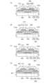
図1(A)乃至図1(C)にトランジスタ300の構成例を示す。図1(A)は、トラン
ジスタ300の平面図であり、図1(B)は、図1(A)中の鎖線X1-Y1における断
面図であり、図1(C)は、図1(A)中の鎖線V1-W1における断面図である。1A to 1C show a configuration example of a
トランジスタ300は、絶縁表面を有する基板400上に設けられたゲート電極層402
と、ゲート電極層402上のゲート絶縁層404と、ゲート絶縁層404上に接し、ゲー
ト電極層402と重畳する酸化物半導体層408と、酸化物半導体層408と電気的に接
続するソース電極層410a及びドレイン電極層410bと、を含む。The
a
トランジスタ300において、ゲート絶縁層404は、ゲート電極層402と接するゲー
ト絶縁層404aと、ゲート絶縁層404a上のゲート絶縁層404bと、を含んで構成
される。In the
ゲート絶縁層404a及びゲート絶縁層404bとして窒素を含むシリコン膜を適用する
。窒素を含むシリコン膜は、酸化シリコン膜と比較して比誘電率が高く、同等の静電容量
を得るのに必要な膜厚が大きいため、ゲート絶縁層を物理的に厚膜化することができる。
よって、トランジスタ300の絶縁耐圧の低下を抑制、さらには絶縁耐圧を向上させて、
半導体装置の静電破壊を抑制することができる。A silicon film containing nitrogen is used as the
Therefore, the decrease in the dielectric strength of the
It is possible to suppress electrostatic damage to the semiconductor device.
窒素を含むシリコン膜としては、例えば、窒化シリコン膜、窒化酸化シリコン膜、酸化窒
化シリコン膜が挙げられるが、窒素の含有量が多い程高い比誘電率を有するため、窒化シ
リコン膜を適用することが好ましい。また、酸化シリコンのエネルギーギャップが8eV
であるのに対して窒化シリコンのエネルギーギャップは5.5eVと小さく、それに応じ
て固有抵抗も小さいため、窒化シリコン膜を用いることでより高いESD耐性を付与する
ことが可能となる。さらに、窒化シリコン膜をCVD法で成膜する場合、窒化酸化シリコ
ン膜等の酸素と窒素を含むシリコン膜をCVD法で成膜する場合に適用される温室効果ガ
スであるN2Oガスを用いる必要がない。なお、本明細書中において、酸化窒化シリコン
膜とは、その組成として、窒素よりも酸素の含有量が多い膜を指し、窒化酸化シリコン膜
とは、その組成として、酸素よりも窒素の含有量が多い膜を指す。Examples of silicon films containing nitrogen include silicon nitride films, silicon nitride oxide films, and silicon oxynitride films. Since the higher the nitrogen content, the higher the relative dielectric constant, it is preferable to use a silicon nitride film. In addition, the energy gap of silicon oxide is 8 eV.
In contrast, the energy gap of silicon nitride is as small as 5.5 eV, and the specific resistance is accordingly small, so that the use of a silicon nitride film can provide higher ESD resistance. Furthermore, when forming a silicon nitride film by a CVD method, there is no need to use N2 O gas, which is a greenhouse gas that is applied when forming a silicon film containing oxygen and nitrogen, such as a silicon nitride oxide film, by a CVD method. In this specification, a silicon oxynitride film refers to a film whose composition contains more oxygen than nitrogen, and a silicon nitride oxide film refers to a film whose composition contains more nitrogen than oxygen.
本実施の形態において、ゲート絶縁層404a及びゲート絶縁層404bとしては、窒化
シリコン膜を適用する。In this embodiment, a silicon nitride film is used as the
ゲート絶縁層404aは、ゲート絶縁層404bよりも厚い膜厚を有し、膜中欠陥が低減
された窒化シリコン膜を用いるものとする。例えば、ゲート絶縁層404aの膜厚を30
0nm以上400nm以下とする。また、電子スピン共鳴法(ESR:Electron
Spin Resonance)においてNcセンター(g値が2.003)に現れる
信号に対応するスピン密度が、好ましくは1×10¹⁷spins/cm3以下、より好
ましくは5×10¹⁶spins/cm3以下である窒化シリコン膜を適用する。このよ
うに、膜中欠陥が低減された窒化シリコン膜を厚い膜厚(例えば、300nm以上)で設
けることにより、ゲート絶縁層404aの絶縁耐圧を、例えば300V以上とすることが
可能である。The
The thickness is set to 0 nm or more and 400 nm or less.
A silicon nitride film is applied in which the spin density corresponding to a signal appearing at the Nc center (g value is 2.003) in the Nc spin resonance is preferably 1×10¹⁷ spins/cm3 or less, more preferably 5×10¹⁶ spins/cm3 or less. By providing a silicon nitride film with reduced in-film defects in this way with a large thickness (e.g., 300 nm or more), it is possible to make the dielectric strength of the
また、ゲート絶縁層404bは、酸化物半導体層408と接するため、含有水素濃度の低
減された窒化シリコン膜とする。ゲート絶縁層404bの水素濃度は、少なくともゲート
絶縁層404aよりも低い濃度とする。例えば、プラズマCVD法により、ゲート絶縁層
404a及びゲート絶縁層404bを成膜する場合に、供給ガス中に含まれる水素濃度を
低下させることで、ゲート絶縁層404bの水素濃度をゲート絶縁層404aよりも低減
することができる。具体的には、ゲート絶縁層404a及びゲート絶縁層404bとして
窒化シリコン膜を形成する場合には、ゲート絶縁層404a成膜のための供給ガスよりも
アンモニア流量を低減、またはアンモニアを用いずにゲート絶縁層404bを成膜すれば
よい。Further, the
また、ゲート絶縁層404bの膜厚は25nm以上150nm以下とする。ゲート絶縁層
404bとして含有水素濃度が低減された窒化シリコン膜を設けることで、酸化物半導体
層408への水素、又は水素化合物(例えば、水)の混入を低減することができる。水素
は酸化物半導体中でキャリアの生成要因となり、トランジスタのしきい値電圧をマイナス
方向に変動(シフト)させる要因となるため、水素濃度の低減された窒化シリコン膜をゲ
ート絶縁層404bとして設けることで、トランジスタの電気特性を安定化させることが
できる。また、水素濃度の低減された窒化シリコン膜をゲート絶縁層404bとして設け
ることで、ゲート絶縁層404aに含有される水素又は水素化合物等の不純物の酸化物半
導体層408への拡散を防止するバリア膜としての効果も奏する。The thickness of the
なお、本実施の形態において、ゲート絶縁層404aとゲート絶縁層404bはともに窒
化シリコン膜であり、材料や成膜条件によっては、各ゲート絶縁層同士の界面が不明確に
なる場合もある。よって、図1においては、ゲート絶縁層404aとゲート絶縁層404
bの界面を模式的に点線で図示している。これは以降の各図面においても同様である。In this embodiment, the
The interface of b is shown by a dotted line in the same manner in the subsequent drawings.
以下では、酸化物半導体層の構造について説明する。The structure of the oxide semiconductor layer is described below.
酸化物半導体層は、単結晶酸化物半導体層と非単結晶酸化物半導体層とに大別される。非
単結晶酸化物半導体層とは、非晶質酸化物半導体層、微結晶酸化物半導体層、多結晶酸化
物半導体層、CAAC-OS(C Axis Aligned Crystalline
Oxide Semiconductor)膜などをいう。The oxide semiconductor layer is roughly classified into a single-crystal oxide semiconductor layer and a non-single-crystal oxide semiconductor layer. The non-single-crystal oxide semiconductor layer includes an amorphous oxide semiconductor layer, a microcrystalline oxide semiconductor layer, a polycrystalline oxide semiconductor layer, and a CAAC-OS (C Axis Aligned Crystalline)
This refers to films such as oxide semiconductor films.
非晶質酸化物半導体層は、膜中における原子配列が不規則であり、結晶成分を有さない酸
化物半導体層である。微小領域においても結晶部を有さず、膜全体が完全な非晶質構造の
酸化物半導体層が典型である。The amorphous oxide semiconductor layer is an oxide semiconductor layer in which the atomic arrangement in the film is irregular and does not include a crystalline component, and is typically an oxide semiconductor layer in which no crystalline part is included even in a microscopic region and the entire film has a completely amorphous structure.
微結晶酸化物半導体層は、例えば、1nm以上10nm未満の大きさの微結晶(ナノ結晶
ともいう。)を含む。従って、微結晶酸化物半導体層は、非晶質酸化物半導体層よりも原
子配列の規則性が高い。そのため、微結晶酸化物半導体層は、非晶質酸化物半導体層より
も欠陥準位密度が低いという特徴がある。The microcrystalline oxide semiconductor layer includes, for example, microcrystals (also referred to as nanocrystals) having a size of 1 nm or more and less than 10 nm. Therefore, the microcrystalline oxide semiconductor layer has a higher degree of regularity in atomic arrangement than an amorphous oxide semiconductor layer. Therefore, the microcrystalline oxide semiconductor layer has a lower density of defect states than an amorphous oxide semiconductor layer.
CAAC-OS膜は、複数の結晶部を有する酸化物半導体層の一つであり、ほとんどの結
晶部は、一辺が100nm未満の立方体内に収まる大きさである。従って、CAAC-O
S膜に含まれる結晶部は、一辺が10nm未満、5nm未満または3nm未満の立方体内
に収まる大きさの場合も含まれる。CAAC-OS膜は、微結晶酸化物半導体層よりも欠
陥準位密度が低いという特徴がある。以下、CAAC-OS膜について詳細な説明を行う
。The CAAC-OS film is one of the oxide semiconductor layers having a plurality of crystal parts, and most of the crystal parts fit within a cube with one side less than 100 nm.
The crystal parts included in the S film may be contained within a cube having one side of less than 10 nm, less than 5 nm, or less than 3 nm. The CAAC-OS film has a feature of having a lower density of defect states than a microcrystalline oxide semiconductor layer. The CAAC-OS film will be described in detail below.
CAAC-OS膜を透過型電子顕微鏡(TEM:Transmission Elect
ron Microscope)によって観察すると、結晶部同士の明確な境界、即ち結
晶粒界(グレインバウンダリーともいう。)を確認することができない。そのため、CA
AC-OS膜は、結晶粒界に起因する電子移動度の低下が起こりにくいといえる。The CAAC-OS film was observed using a transmission electron microscope (TEM).
When observed with a C.A.R.O. Microscope, it is not possible to confirm clear boundaries between crystalline portions, i.e., grain boundaries.
It can be said that in the AC-OS film, a decrease in electron mobility caused by crystal grain boundaries is unlikely to occur.
CAAC-OS膜を、試料面と概略平行な方向からTEMによって観察(断面TEM観察
)すると、結晶部において、金属原子が層状に配列していることを確認できる。金属原子
の各層は、CAAC-OS膜の膜を形成する面(被形成面ともいう。)または上面の凹凸
を反映した形状であり、CAAC-OS膜の被形成面または上面と平行に配列する。When the CAAC-OS film is observed by a TEM from a direction approximately parallel to the sample surface (cross-sectional TEM observation), it can be seen that metal atoms are arranged in layers in the crystal part. Each layer of metal atoms has a shape that reflects the unevenness of the surface (also referred to as the surface on which the CAAC-OS film is formed) or the top surface of the CAAC-OS film, and is arranged in parallel to the surface on which the CAAC-OS film is formed or the top surface.
なお、本明細書において、「平行」とは、二つの直線が-10°以上10°以下の角度で
配置されている状態をいう。従って、-5°以上5°以下の場合も含まれる。また、「垂
直」とは、二つの直線が80°以上100°以下の角度で配置されている状態をいう。従
って、85°以上95°以下の場合も含まれる。In this specification, "parallel" refers to a state in which two straight lines are arranged at an angle of -10° or more and 10° or less. Therefore, it also includes the case of -5° or more and 5° or less. Furthermore, "perpendicular" refers to a state in which two straight lines are arranged at an angle of 80° or more and 100° or less. Therefore, it also includes the case of 85° or more and 95° or less.
一方、CAAC-OS膜を、試料面と概略垂直な方向からTEMによって観察(平面TE
M観察)すると、結晶部において、金属原子が三角形状または六角形状に配列しているこ
とを確認できる。しかしながら、異なる結晶部間で、金属原子の配列に規則性は見られな
い。On the other hand, the CAAC-OS film was observed by TEM from a direction approximately perpendicular to the sample surface (planar TEM).
When the metal atoms are aligned in the crystal regions, it can be seen that they are arranged in triangular or hexagonal shapes. However, no regularity is observed in the arrangement of the metal atoms between different crystal regions.
断面TEM観察および平面TEM観察より、CAAC-OS膜の結晶部は配向性を有して
いることがわかる。Cross-sectional and planar TEM observations reveal that the crystal parts of the CAAC-OS film have orientation.
CAAC-OS膜に対し、X線回折(XRD:X-Ray Diffraction)装
置を用いて構造解析を行うと、例えばInGaZnO4の結晶を有するCAAC-OS膜
のout-of-plane法による解析では、回折角(2θ)が31°近傍にピークが
現れる場合がある。このピークは、InGaZnO4の結晶の(009)面に帰属される
ことから、CAAC-OS膜の結晶がc軸配向性を有し、c軸が被形成面または上面に概
略垂直な方向を向いていることが確認できる。When a CAAC-OS film is subjected to structural analysis using an X-ray diffraction (XRD) apparatus, for example, a peak may appear at a diffraction angle (2θ) of about 31° in an out-of-plane analysis of a CAAC-OS film having InGaZnO4 crystals. This peak is attributed to the (009) plane of the InGaZnO4 crystals, and therefore it can be confirmed that the crystals of the CAAC-OS film have c-axis orientation and the c-axis faces in a direction approximately perpendicular to the surface on which the CAAC-OS film is formed or the top surface.
一方、CAAC-OS膜に対し、c軸に概略垂直な方向からX線を入射させるin-pl
ane法による解析では、2θが56°近傍にピークが現れる場合がある。このピークは
、InGaZnO4の結晶の(110)面に帰属される。InGaZnO4の単結晶酸化
物半導体層であれば、2θを56°近傍に固定し、試料面の法線ベクトルを軸(φ軸)と
して試料を回転させながら分析(φスキャン)を行うと、(110)面と等価な結晶面に
帰属されるピークが6本観察される。これに対し、CAAC-OS膜の場合は、2θを5
6°近傍に固定してφスキャンした場合でも、明瞭なピークが現れない。On the other hand, in-plane X-ray irradiation is performed on the CAAC-OS film in a direction substantially perpendicular to the c-axis.
In the analysis by the AN method, a peak may appear when 2θ is around 56°. This peak is attributed to the (110) plane of the InGaZnO4 crystal. In the case of a single crystal oxide semiconductor layer of InGaZnO4 , when 2θ is fixed at around 56° and analysis (φ scan) is performed while rotating the sample around the axis (φ axis) of the normal vector of the sample surface, six peaks attributed to a crystal plane equivalent to the (110) plane are observed. In contrast, in the case of a CAAC-OS film, when 2θ is fixed at around 56°, six peaks attributed to a crystal plane equivalent to the (110) plane are observed.
Even when φ is fixed at around 6° and scanned, no clear peak appears.
以上のことから、CAAC-OS膜では、異なる結晶部間ではa軸およびb軸の配向は不
規則であるが、c軸配向性を有し、かつc軸が被形成面または上面の法線ベクトルに平行
な方向を向いていることがわかる。従って、前述の断面TEM観察で確認された層状に配
列した金属原子の各層は、結晶のab面に平行な面である。From the above, it can be seen that the orientation of the a-axis and the b-axis is irregular between different crystal parts in the CAAC-OS film, but the film has a c-axis orientation, and the c-axis is parallel to the normal vector of the surface on which the film is formed or the top surface. Therefore, each layer of metal atoms arranged in layers confirmed by the above-mentioned cross-sectional TEM observation is a plane parallel to the a-b plane of the crystal.
なお、結晶部は、CAAC-OS膜を成膜した際、または加熱処理などの結晶化処理を行
った際に形成される。上述したように、結晶のc軸は、CAAC-OS膜の被形成面また
は上面の法線ベクトルに平行な方向に配向する。従って、例えば、CAAC-OS膜の形
状をエッチングなどによって変化させた場合、結晶のc軸がCAAC-OS膜の被形成面
または上面の法線ベクトルと平行にならないこともある。The crystalline parts are formed when the CAAC-OS film is formed or when a crystallization treatment such as heat treatment is performed. As described above, the c-axis of the crystal is oriented in a direction parallel to the normal vector of the surface on which the CAAC-OS film is formed or the top surface. Therefore, for example, when the shape of the CAAC-OS film is changed by etching or the like, the c-axis of the crystal may not be parallel to the normal vector of the surface on which the CAAC-OS film is formed or the top surface.
また、CAAC-OS膜中の結晶化度が均一でなくてもよい。例えば、CAAC-OS膜
の結晶部が、CAAC-OS膜の上面近傍からの結晶成長によって形成される場合、上面
近傍の領域は、被形成面近傍の領域よりも結晶化度が高くなることがある。また、CAA
C-OS膜に不純物を添加する場合、不純物が添加された領域の結晶化度が変化し、部分
的に結晶化度の異なる領域が形成されることもある。The degree of crystallinity in the CAAC-OS film does not have to be uniform. For example, when a crystalline portion of the CAAC-OS film is formed by crystal growth from the vicinity of the top surface of the CAAC-OS film, the degree of crystallinity in the vicinity of the top surface may be higher than that in the vicinity of the surface on which the CAAC-OS film is formed.
When an impurity is added to a C-OS film, the degree of crystallinity of a region to which the impurity is added may change, and a region having a different degree of crystallinity may be formed partially.
なお、InGaZnO4の結晶を有するCAAC-OS膜のout-of-plane法
による解析では、2θが31°近傍のピークの他に、2θが36°近傍にもピークが現れ
る場合がある。2θが36°近傍のピークは、CAAC-OS膜中の一部に、c軸配向性
を有さない結晶が含まれることを示している。CAAC-OS膜は、2θが31°近傍に
ピークを示し、2θが36°近傍にピークを示さないことが好ましい。In addition, in an out-of-plane analysis of a CAAC-OS film containing InGaZnO4 crystals, a peak may appear at 2θ near 36° in addition to the peak at 2θ near 31°. The peak at 2θ near 36° indicates that crystals without c-axis orientation are contained in part of the CAAC-OS film. It is preferable that the CAAC-OS film shows a peak at 2θ near 31° and does not show a peak at 2θ near 36°.
なお、本明細書において、結晶が三方晶または菱面体晶である場合、六方晶系として表す
。In this specification, when the crystal is a trigonal or rhombohedral crystal, it is represented as a hexagonal crystal system.
CAAC-OS膜を用いたトランジスタは、可視光や紫外光の照射による電気特性の変動
が小さい。よって、当該トランジスタは、信頼性が高い。A transistor including a CAAC-OS film has small changes in electrical characteristics due to irradiation with visible light or ultraviolet light, and thus has high reliability.
なお、酸化物半導体層408は、例えば、非晶質酸化物半導体層、微結晶酸化物半導体層
、CAAC-OS膜のいずれの構造であってもよいし、これらの構造のうち二種以上を含
んでいてもよい。またこれらの構造のうち、二種以上を有する積層膜であってもよい。Note that the
CAAC-OS膜は、例えば、多結晶である酸化物半導体スパッタリング用ターゲットを
用い、スパッタリング法によって成膜する。当該スパッタリング用ターゲットにイオンが
衝突すると、スパッタリング用ターゲットに含まれる結晶領域がa-b面から劈開し、a
-b面に平行な面を有する平板状またはペレット状のスパッタリング粒子として剥離する
ことがある。この場合、当該平板状のスパッタリング粒子が、結晶状態を維持したまま基
板に到達することで、CAAC-OS膜を成膜することができる。The CAAC-OS film is formed by a sputtering method using a polycrystalline oxide semiconductor sputtering target. When ions collide with the sputtering target, a crystalline region included in the sputtering target is cleaved from the a-b plane.
The sputtered particles may be peeled off as flat or pellet-like sputtered particles having a surface parallel to the -b plane. In this case, the flat sputtered particles reach the substrate while maintaining their crystalline state, thereby forming a CAAC-OS film.
また、CAAC-OS膜を成膜するために、以下の条件を適用することが好ましい。In addition, it is preferable to apply the following conditions to form a CAAC-OS film.
成膜時の不純物混入を低減することで、不純物によって結晶状態が崩れることを抑制でき
る。例えば、成膜室内に存在する不純物濃度(水素、水、二酸化炭素および窒素など)を
低減すればよい。また、成膜ガス中の不純物濃度を低減すればよい。具体的には、露点が
-80℃以下、好ましくは-100℃以下である成膜ガスを用いる。By reducing the amount of impurities mixed in during film formation, it is possible to prevent the crystal state from being destroyed by the impurities. For example, the concentration of impurities (hydrogen, water, carbon dioxide, nitrogen, etc.) present in the film formation chamber may be reduced. In addition, the concentration of impurities in the film formation gas may be reduced. Specifically, a film formation gas having a dew point of -80°C or less, preferably -100°C or less, may be used.
また、成膜時の基板加熱温度を高めることで、基板付着後にスパッタリング粒子のマイグ
レーションが起こる。具体的には、基板加熱温度を100℃以上740℃以下、好ましく
は200℃以上500℃以下として成膜する。成膜時の基板加熱温度を高めることで、平
板状のスパッタリング粒子が基板に到達した場合、基板上でマイグレーションが起こり、
スパッタリング粒子の平らな面が基板に付着する。In addition, by increasing the substrate heating temperature during film formation, migration of sputtered particles occurs after deposition on the substrate. Specifically, the substrate heating temperature is set to 100° C. or higher and 740° C. or lower, preferably 200° C. or higher and 500° C. or lower, and film formation is performed. By increasing the substrate heating temperature during film formation, when flat sputtered particles reach the substrate, migration occurs on the substrate,
The flat surface of the sputtered particle adheres to the substrate.
また、成膜ガス中の酸素割合を高め、電力を最適化することで成膜時のプラズマダメージ
を軽減すると好ましい。成膜ガス中の酸素割合は、30体積%以上、好ましくは100体
積%とする。It is also preferable to reduce plasma damage during film formation by increasing the oxygen ratio in the film formation gas and optimizing the power. The oxygen ratio in the film formation gas is set to 30 volume % or more, preferably 100 volume %.
スパッタリング用ターゲットの一例として、In-Ga-Zn-O化合物ターゲットにつ
いて以下に示す。As an example of a sputtering target, an In--Ga--Zn--O compound target will be described below.
InOX粉末、GaOY粉末およびZnOZ粉末を所定の比率で混合し、加圧処理後、1
000℃以上1500℃以下の温度で加熱処理をすることで多結晶であるIn-Ga-Z
n-O化合物ターゲットとする。なお、X、YおよびZは任意の正数である。ここで、所
定のmol数比は、例えば、InOX粉末、GaOY粉末およびZnOZ粉末が、2:2
:1、8:4:3、3:1:1、1:1:1、4:2:3または3:1:2である。なお
、粉末の種類、およびその混合するmol数比は、作製するスパッタリング用ターゲット
によって適宜変更すればよい。InOX powder, GaOY powder and ZnOZ powder are mixed in a predetermined ratio, pressurized, and then cooled.
By performing heat treatment at a temperature of 000°C or higher and 1500°C or lower, polycrystalline In-Ga-Z
The n-O compound target is a mixture of InOX powder, GaOY powder, and ZnOZ powder in a ratio of 2:2.
The molar ratio of the powders may be appropriately changed depending on the sputtering target to be produced.
トランジスタ300の構成要素として、ソース電極層410a及びドレイン電極層410
bを覆い、酸化物半導体層408と接する絶縁層414を含めてもよい。As components of the
b and in contact with the
絶縁層414としては、酸化シリコン膜、酸化ガリウム膜、酸化アルミニウム膜、窒化シ
リコン膜、酸化窒化シリコン膜、酸化窒化アルミニウム膜、または窒化酸化シリコン膜等
を用いることができる。但し、絶縁層414を、窒素を含むシリコン膜、より好ましくは
窒化シリコン膜とすることで、半導体装置の作製工程中、又は、形成後の半導体装置に対
する静電破壊をより低減することが可能となるため、好ましい。A silicon oxide film, a gallium oxide film, an aluminum oxide film, a silicon nitride film, a silicon oxynitride film, an aluminum oxynitride film, a silicon nitride oxide film, or the like can be used as the insulating
以下に、図2を用いてトランジスタ300の作製方法の一例を示す。Below, an example of a method for manufacturing the
まず、絶縁表面を有する基板400上に、ゲート電極層402を形成する。First, a
絶縁表面を有する基板400に使用することができる基板に大きな制約はないが、少なく
とも後の熱処理に耐えうる程度の耐熱性を有することが必要となる。例えば、バリウムホ
ウケイ酸ガラスやアルミノホウケイ酸ガラス等のガラス基板、セラミック基板、石英基板
、サファイヤ基板などを用いることができる。また、シリコンや炭化シリコン等の単結晶
半導体基板、多結晶半導体基板、シリコンゲルマニウム等の化合物半導体基板、SOI基
板等を適用することができ、これらの基板に半導体素子が設けられたものを基板400と
して用いてもよい。There are no significant restrictions on the substrate that can be used for the
ゲート電極層402は、モリブデン、チタン、タンタル、タングステン、アルミニウム、
銅、クロム、ネオジム、スカンジウム等の金属材料又はこれらを主成分とする合金材料を
用いて形成することができる。また、ゲート電極層402としてリン等の不純物元素をド
ーピングした多結晶シリコン膜に代表される半導体膜、ニッケルシリサイド等のシリサイ
ド膜を用いてもよい。ゲート電極層402は単層構造としてもよいし、積層構造としても
よい。ゲート電極層402はテーパ形状としてもよく、例えばテーパ角を30°以上70
°以下とすればよい。ここで、テーパ角とは、テーパ形状を有する層の側面と、当該層の
底面との間の角度を指す。The
The
The taper angle may be set to 0° or less. Here, the taper angle refers to the angle between the side surface of a layer having a tapered shape and the bottom surface of the layer.
また、ゲート電極層402の材料は、酸化インジウム酸化スズ、酸化タングステンを含む
インジウム酸化物、酸化タングステンを含むインジウム亜鉛酸化物、酸化チタンを含むイ
ンジウム酸化物、酸化チタンを含むインジウムスズ酸化物、酸化インジウム酸化亜鉛、酸
化ケイ素を添加したインジウムスズ酸化物等の導電性材料を適用することもできる。The
または、ゲート電極層402の材料として、窒素を含むIn-Ga-Zn系酸化物、窒素
を含むIn-Sn系酸化物、窒素を含むIn-Ga系酸化物、窒素を含むIn-Zn系酸
化物、窒素を含むSn系酸化物、窒素を含むIn系酸化物、金属窒化物(窒化インジウム
、窒化亜鉛、窒化タンタル、窒化タングステンなど)を用いてもよい。これらの材料は、
5eV以上の仕事関数を有するため、これらの材料を用いてゲート電極層402を形成す
ることでトランジスタのしきい値電圧をプラスにすることができ、ノーマリオフのスイッ
チングトランジスタを実現できる。Alternatively, the
Since these materials have a work function of 5 eV or more, the threshold voltage of the transistor can be made positive by forming the
次いで、ゲート電極層402を覆うように、ゲート絶縁層404a及びゲート絶縁層40
4bを含むゲート絶縁層404を形成する(図2(A)参照)。ゲート絶縁層404とし
ては、窒素を含むシリコン膜を適用することができる。本実施の形態では、窒化シリコン
膜でなるゲート絶縁層404aと窒化シリコン膜でなるゲート絶縁層404bを積層させ
てゲート絶縁層404とする。ゲート絶縁層404は、面内バラツキ、パーティクル混入
および成膜タクトを低減する観点から、CVD法を用いて成膜を行うことが効果的である
。また、CVD法は、大面積基板に対する成膜についても効果的である。Next, the
A
本実施の形態では、プラズマCVD法によってゲート絶縁層404a及びゲート絶縁層4
04bを連続的に形成する。まず、供給ガスをシラン(SiH4)、窒素(N2)及びア
ンモニア(NH3)の混合ガスとして、ゲート絶縁層404aとなる窒化シリコン膜を成
膜し、その後、供給ガスを、シラン(SiH4)と窒素(N2)の混合ガスに切り替えて
、ゲート絶縁層404bとなる窒化シリコン膜を成膜する。In this embodiment, the
First, a silicon nitride film that will become the
プラズマCVD法の供給ガスをシラン(SiH4)、窒素(N2)及びアンモニア(NH
3)の混合ガスとして成膜された窒化シリコン膜は、供給ガスをシラン(SiH4)と窒
素(N2)の混合ガスとして成膜された窒化シリコン膜よりも膜中欠陥を低減することが
できる。よって、ゲート絶縁層404aは、少なくともゲート絶縁層404bよりも膜中
欠陥の低減された膜であり、例えば、電子スピン共鳴法(ESR)においてNcセンター
(g値が2.003)に現れる信号に対応するスピン密度を、好ましくは1×10¹⁷s
pins/cm3、より好ましくは5×1016spins/cm3以下とすることがで
きる。また、混合ガスにアンモニアを含んで成膜された窒化シリコン膜は、供給ガスをシ
ランと窒素の混合ガスとした場合よりも被覆性の良好な膜とすることができるため、ゲー
ト電極層402に接するゲート絶縁層として、上述の混合ガスを用いた窒化シリコン膜を
設けることは有効である。また、膜中欠陥の低減されたゲート絶縁層404aを膜厚30
0nm以上400nm以下で設けることで、ゲート絶縁層404の絶縁耐圧を300V以
上とすることができる。The supply gas for the plasma CVD method was silane (SiH4 ), nitrogen (N2 ), and ammonia (NH
A silicon nitride film formed using a mixed gas of silane (SiH4 ) and nitrogen (N2 ) as a supply gas can reduce defects in the film more than a silicon nitride film formed using a mixed gas of silane (SiH 4 ) and nitrogen (N 2) . Therefore, the
The concentration of the silicon nitride film formed using the mixed gas containing ammonia can be more preferably 5×10¹⁶ spins/cm3or less. Since a silicon nitride film formed using the mixed gas containing ammonia can have better coverage than a film formed using a mixed gas of silane and nitrogen as a supply gas, it is effective to provide a silicon nitride film using the above-mentioned mixed gas as a gate insulating layer in contact with the
When the
一方、材料ガス中にアンモニアを含まずに成膜されたゲート絶縁層404bは、ゲート絶
縁層404aと比較して含有水素濃度が低い膜とすることができる。このような膜を酸化
物半導体層408と接する態様で設けることで、ゲート絶縁層404bから酸化物半導体
層408への水素の混入を低減することができる。また、ゲート絶縁層404bは、ゲー
ト絶縁層404aに含まれる水素又は水素化合物が、酸化物半導体層408への混入する
ことを抑制するバリア膜としても機能する。On the other hand, the
ゲート絶縁層404として、膜中欠陥の低減された厚膜のゲート絶縁層404aと、水素
濃度の低減されたゲート絶縁層404bとを積層することで、絶縁耐圧を良好としつつ、
酸化物半導体層408への水素等の不純物の拡散を抑制することができる。よって、当該
ゲート絶縁層404を含むトランジスタの静電破壊を抑制し、且つ、電気特性を安定化さ
せることが可能となる。As the
It is possible to suppress diffusion of impurities such as hydrogen into the
次いで、ゲート絶縁層404b上に酸化物半導体層を形成し、エッチング処理によって島
状に加工して、酸化物半導体層408を形成する(図2(B)参照)。Next, an oxide semiconductor layer is formed over the
酸化物半導体層408は、非晶質構造であってもよいし、結晶性であってもよい。成膜後
の酸化物半導体層を非晶質構造とする場合には、後の作製工程において熱処理を加えるこ
とで結晶性の酸化物半導体層408としてもよい。非晶質酸化物半導体層を結晶化させる
熱処理の温度は、250℃以上700℃以下、好ましくは400℃以上、より好ましくは
500℃以上、さらに好ましくは550℃以上とする。なお、当該熱処理は、作製工程に
おける他の熱処理と兼ねることも可能である。The
酸化物半導体層408の成膜方法は、スパッタリング法、MBE(Molecular
Beam Epitaxy)法、CVD法、パルスレーザ堆積法、ALD(Atomic
Layer Deposition)法等を適宜用いることができる。The
Beam Epitaxy method, CVD method, pulsed laser deposition method, ALD (Atomic
A layer deposition method or the like can be appropriately used.
酸化物半導体層408を成膜する際、できる限り膜中に含まれる水素濃度を低減させるこ
とが好ましい。水素濃度を低減させるには、例えば、スパッタリング法を用いて成膜を行
う場合には、スパッタリング装置の成膜室内に供給する雰囲気ガスとして、水素、水、水
酸基又は水素化物などの不純物が除去された高純度の希ガス(代表的にはアルゴン)、酸
素、及び希ガスと酸素との混合ガスを適宜用いる。It is preferable to reduce the hydrogen concentration in the film as much as possible when the
また、成膜室内の残留水分を除去しつつ水素及び水分が除去されたスパッタガスを導入し
て成膜を行うことで、成膜された酸化物半導体層の水素濃度を低減させることができる。
成膜室内の残留水分を除去するためには、吸着型の真空ポンプ、例えば、クライオポンプ
、イオンポンプ、チタンサブリメーションポンプを用いることが好ましい。また、ターボ
分子ポンプにコールドトラップを加えたものであってもよい。クライオポンプは、例えば
、水素分子、水(H2O)など水素原子を含む化合物(より好ましくは炭素原子を含む化
合物も)等の排気能力が高いため、クライオポンプを用いて排気した成膜室で成膜した膜
中に含まれる不純物の濃度を低減できる。Furthermore, when the film is formed by introducing a sputtering gas from which hydrogen and moisture have been removed while removing moisture remaining in the film formation chamber, the hydrogen concentration in the formed oxide semiconductor layer can be reduced.
In order to remove the residual moisture in the film forming chamber, it is preferable to use an adsorption type vacuum pump, for example, a cryopump, an ion pump, or a titanium sublimation pump. Alternatively, a turbo molecular pump with a cold trap may be used. Since the cryopump has a high pumping capacity for compounds containing hydrogen atoms, such as hydrogen molecules and water (H2 O) (and more preferably compounds containing carbon atoms), the concentration of impurities contained in the film formed in the film forming chamber evacuated using the cryopump can be reduced.
なお、ゲート絶縁層404及び酸化物半導体層は、大気開放せずに連続的に成膜すること
が好ましい。ゲート絶縁層404及び酸化物半導体層の成膜を大気開放せずに連続的に行
うことで、酸化物半導体層表面への水素又は水素化合物の付着(例えば、吸着水など)を
防止することができるため、不純物の混入を抑制することができる。Note that the
また、酸化物半導体層をスパッタリング法で成膜する場合、成膜に用いる金属酸化物ター
ゲットの相対密度(充填率)は90%以上100%以下、好ましくは95%以上99.9
%以下とする。相対密度の高い金属酸化物ターゲットを用いることにより、成膜される膜
を緻密な膜とすることができる。In addition, when the oxide semiconductor layer is formed by a sputtering method, the relative density (filling rate) of a metal oxide target used for the film formation is 90% or more and 100% or less, preferably 95% or more and 99.9% or less.
By using a metal oxide target with a high relative density, the deposited film can be made dense.
なお、基板400を高温に保持した状態で酸化物半導体層を形成することも、酸化物半導
体層中に含まれうる不純物濃度を低減するのに有効である。基板400を加熱する温度と
しては、150℃以上450℃以下とすればよく、好ましくは基板温度を200℃以上3
50℃以下とすればよい。また、成膜時に基板を高温で加熱することで、結晶性酸化物半
導体層を形成することができる。Note that forming the oxide semiconductor layer while the
The temperature may be less than or equal to 50° C. In addition, a crystalline oxide semiconductor layer can be formed by heating the substrate at a high temperature during film formation.
酸化物半導体層408としてCAAC-OS膜を適用する場合、該CAAC-OS膜を得
る方法としては、例えば、成膜温度を200℃以上450℃以下として酸化物半導体層の
成膜を行い、表面に概略垂直にc軸配向させる方法がある。または、酸化物半導体層を薄
い膜厚で成膜した後、200℃以上700℃以下の熱処理を行い、表面に概略垂直にc軸
配向させてもよい。または、一層目として薄い膜厚で成膜した後、200℃以上700℃
以下の熱処理を行い、二層目の成膜を行い、表面に概略垂直にc軸配向させてもよい。When a CAAC-OS film is used as the
The following heat treatment may be carried out to form a second layer, and the c-axis may be oriented approximately perpendicular to the surface.
酸化物半導体層408に用いる酸化物半導体としては、少なくともインジウム(In)を
含む。特に、インジウムと亜鉛(Zn)を含むことが好ましい。また、該酸化物半導体を
用いたトランジスタの電気特性のばらつきを減らすためのスタビライザーとして、それら
に加えてガリウム(Ga)を有することが好ましい。また、スタビライザーとしてスズ(
Sn)、ハフニウム(Hf)、アルミニウム(Al)、ジルコニウム(Zr)のいずれか
一種または複数種を有することが好ましい。The oxide semiconductor used for the
It is preferable that the material contains one or more of the following: Sn), hafnium (Hf), aluminum (Al), and zirconium (Zr).
また、他のスタビライザーとして、ランタノイドである、ランタン(La)、セリウム(
Ce)、プラセオジム(Pr)、ネオジム(Nd)、サマリウム(Sm)、ユウロピウム
(Eu)、ガドリニウム(Gd)、テルビウム(Tb)、ジスプロシウム(Dy)、ホル
ミウム(Ho)、エルビウム(Er)、ツリウム(Tm)、イッテルビウム(Yb)、ル
テチウム(Lu)のいずれか一種または複数種を有してもよい。Other stabilizers include lanthanides such as lanthanum (La) and cerium (
The element may have one or more of the following: arsenic (Ce), praseodymium (Pr), neodymium (Nd), samarium (Sm), europium (Eu), gadolinium (Gd), terbium (Tb), dysprosium (Dy), holmium (Ho), erbium (Er), thulium (Tm), ytterbium (Yb), and lutetium (Lu).
例えば、酸化物半導体として、酸化インジウム、酸化スズ、酸化亜鉛、二元系金属の酸化
物であるIn-Zn系酸化物、In-Mg系酸化物、In-Ga系酸化物、三元系金属の
酸化物であるIn-Ga-Zn系酸化物、In-Al-Zn系酸化物、In-Sn-Zn
系酸化物、In-Hf-Zn系酸化物、In-La-Zn系酸化物、In-Ce-Zn系
酸化物、In-Pr-Zn系酸化物、In-Nd-Zn系酸化物、In-Sm-Zn系酸
化物、In-Eu-Zn系酸化物、In-Gd-Zn系酸化物、In-Tb-Zn系酸化
物、In-Dy-Zn系酸化物、In-Ho-Zn系酸化物、In-Er-Zn系酸化物
、In-Tm-Zn系酸化物、In-Yb-Zn系酸化物、In-Lu-Zn系酸化物、
四元系金属の酸化物であるIn-Sn-Ga-Zn系酸化物、In-Hf-Ga-Zn系
酸化物、In-Al-Ga-Zn系酸化物、In-Sn-Al-Zn系酸化物、In-S
n-Hf-Zn系酸化物、In-Hf-Al-Zn系酸化物を用いることができる。Examples of oxide semiconductors include indium oxide, tin oxide, zinc oxide, In-Zn oxides, which are oxides of binary metals, In-Mg oxides, In-Ga oxides, In-Ga-Zn oxides, which are oxides of ternary metals, In-Al-Zn oxides, In-Sn-Zn oxides,
based oxides, In-Hf-Zn based oxides, In-La-Zn based oxides, In-Ce-Zn based oxides, In-Pr-Zn based oxides, In-Nd-Zn based oxides, In-Sm-Zn based oxides, In-Eu-Zn based oxides, In-Gd-Zn based oxides, In-Tb-Zn based oxides, In-Dy-Zn based oxides, In-Ho-Zn based oxides, In-Er-Zn based oxides, In-Tm-Zn based oxides, In-Yb-Zn based oxides, In-Lu-Zn based oxides,
Oxides of quaternary metals include In-Sn-Ga-Zn oxides, In-Hf-Ga-Zn oxides, In-Al-Ga-Zn oxides, In-Sn-Al-Zn oxides, In-S
An n-Hf-Zn based oxide or an In-Hf-Al-Zn based oxide can be used.
例えば、In-Ga-Zn系酸化物とは、InとGaとZnを主成分として有する酸化物
という意味であり、InとGaとZnの比率は問わない。また、InとGaとZn以外の
金属元素が入っていてもよい。For example, an In-Ga-Zn oxide means an oxide having In, Ga, and Zn as main components, regardless of the ratio of In, Ga, and Zn. Also, metal elements other than In, Ga, and Zn may be included.
また、酸化物半導体として、InMO3(ZnO)m(m>0、且つ、mは整数でない)
で表記される材料を用いてもよい。なお、Mは、Ga、Fe、MnおよびCoから選ばれ
た一の金属元素または複数の金属元素を示す。また、酸化物半導体として、In2SnO
5(ZnO)n(n>0、且つ、nは整数)で表記される材料を用いてもよい。In addition, the oxide semiconductor may be InMO3 (ZnO)m (m>0, and m is not an integer).
In addition, M represents one or more metal elements selected from Ga, Fe, Mn, and Co. In addition, as the oxide semiconductor, a material represented by the formula (I ) may be used.
A material expressed asZnO.sup.5 (ZnO)n (n>0, and n is an integer) may also be used.
例えば、In:Ga:Zn=1:1:1(=1/3:1/3:1/3)、In:Ga:Z
n=2:2:1(=2/5:2/5:1/5)、あるいはIn:Ga:Zn=3:1:2
(=1/2:1/6:1/3)の原子数比のIn-Ga-Zn系酸化物やその組成の近傍
の酸化物を用いることができる。あるいは、In:Sn:Zn=1:1:1(=1/3:
1/3:1/3)、In:Sn:Zn=2:1:3(=1/3:1/6:1/2)あるい
はIn:Sn:Zn=2:1:5(=1/4:1/8:5/8)の原子数比のIn-Sn
-Zn系酸化物やその組成の近傍の酸化物を用いるとよい。For example, In:Ga:Zn=1:1:1 (=1/3:1/3:1/3), In:Ga:Z
n=2:2:1 (=2/5:2/5:1/5), or In:Ga:Zn=3:1:2
In-Ga-Zn oxides having an atomic ratio of In:Sn:Zn=1:1:1 (=1/3:1/6:1/3) or oxides having a similar composition can be used.
In-Sn with an atomic ratio of In:Sn:Zn=2:1:3 (=1/3:1/3:1/6:1/2) or In:Sn:Zn=2:1:5 (=1/4:1/8:5/8)
It is preferable to use a -Zn-based oxide or an oxide having a composition close to that.
しかし、インジウムを含む酸化物半導体を用いたトランジスタは、これらに限られず、必
要とする電気的特性(電界効果移動度、しきい値、ばらつき等)に応じて適切な組成のも
のを用いればよい。また、必要とする電気的特性を得るために、キャリア濃度や不純物濃
度、欠陥密度、金属元素と酸素の原子数比、原子間距離、密度等を適切なものとすること
が好ましい。However, the transistor using an oxide semiconductor containing indium is not limited to these, and may have an appropriate composition depending on required electrical characteristics (field-effect mobility, threshold value, variation, etc.) In order to obtain required electrical characteristics, it is preferable to set the carrier concentration, impurity concentration, defect density, atomic ratio of metal element to oxygen, interatomic distance, density, and the like appropriately.
例えば、In-Sn-Zn系酸化物半導体を用いたトランジスタでは比較的容易に高い電
界効果移動度が得られる。しかしながら、In-Ga-Zn系酸化物半導体を用いたトラ
ンジスタでも、バルク内欠陥密度を低くすることにより電界効果移動度を上げることがで
きる。For example, a transistor using an In-Sn-Zn-based oxide semiconductor can relatively easily achieve high field-effect mobility. However, even in a transistor using an In-Ga-Zn-based oxide semiconductor, the field-effect mobility can be increased by reducing the bulk defect density.
なお、例えば、In、Ga、Znの原子数比がIn:Ga:Zn=a:b:c(a+b+
c=1)である酸化物の組成が、原子数比がIn:Ga:Zn=A:B:C(A+B+C
=1)の酸化物の組成の近傍であるとは、a、b、cが、(a-A)2+(b-B)2+
(c-C)2≦r2を満たすことをいう。rとしては、例えば、0.05とすればよい。
他の酸化物でも同様である。For example, the atomic ratio of In, Ga, and Zn is In:Ga:Zn=a:b:c (a+b+
The composition of the oxide in which the atomic ratio is In:Ga:Zn=A:B:C (A+B+C
= 1), a, b, and c are in the vicinity of the oxide composition (a-A)2 + (b-B)2 +
This means that (cC)2 ≦r2 is satisfied, where r is set to, for example, 0.05.
The same is true for other oxides.
また、酸化物半導体層408に対して、膜中に含まれる過剰な水素(水や水酸基を含む)
を除去(脱水化又は脱水素化)するための熱処理を行うことが好ましい。熱処理の温度は
、300℃以上700℃以下、又は基板の歪み点未満とする。熱処理は減圧下又は窒素雰
囲気下などで行うことができる。この熱処理によって、n型の導電性を付与する不純物で
ある水素を除去することができる。In addition, the
It is preferable to perform a heat treatment for removing (dehydrating or dehydrogenating) hydrogen. The temperature of the heat treatment is 300° C. or higher and 700° C. or lower, or lower than the strain point of the substrate. The heat treatment can be performed under reduced pressure or in a nitrogen atmosphere. This heat treatment can remove hydrogen, which is an impurity that imparts n-type conductivity.
なお、脱水化又は脱水素化のための熱処理は、酸化物半導体層の成膜後であればトランジ
スタの作製工程においてどのタイミングで行ってもよい。また、脱水化又は脱水素化のた
めの熱処理は、複数回行ってもよく、他の熱処理と兼ねてもよい。Note that the heat treatment for dehydration or dehydrogenation may be performed at any timing in the manufacturing process of a transistor as long as it is performed after the formation of the oxide semiconductor layer. The heat treatment for dehydration or dehydrogenation may be performed multiple times or may be performed together with other heat treatments.
熱処理においては、窒素、又はヘリウム、ネオン、アルゴン等の希ガスに、水、水素など
が含まれないことが好ましい。又は、熱処理装置に導入する窒素、又はヘリウム、ネオン
、アルゴン等の希ガスの純度を、6N(99.9999%)以上好ましくは7N(99.
99999%)以上(即ち不純物濃度を1ppm以下、好ましくは0.1ppm以下)と
することが好ましい。In the heat treatment, it is preferable that the nitrogen or rare gas such as helium, neon, argon, etc. does not contain water, hydrogen, etc. Alternatively, the purity of the nitrogen or rare gas such as helium, neon, argon, etc. introduced into the heat treatment device is 6N (99.9999%) or more, preferably 7N (99.
99999%) or more (i.e., the impurity concentration is 1 ppm or less, preferably 0.1 ppm or less).
また、熱処理で酸化物半導体層408を加熱した後、加熱温度を維持、又はその加熱温度
から徐冷しながら同じ炉に高純度の酸素ガス、高純度の一酸化二窒素ガス、又は超乾燥エ
ア(CRDS(キャビティリングダウンレーザー分光法)方式の露点計を用いて測定した
場合の水分量が20ppm(露点換算で-55℃)以下、好ましくは1ppm以下、より
好ましくは10ppb以下の空気)を導入してもよい。酸素ガス又は一酸化二窒素ガスに
、水、水素などが含まれないことが好ましい。又は、熱処理装置に導入する酸素ガス又は
一酸化二窒素ガスの純度を、6N以上好ましくは7N以上(即ち、酸素ガス又は一酸化二
窒素ガス中の不純物濃度を1ppm以下、好ましくは0.1ppm以下)とすることが好
ましい。酸素ガス又は一酸化二窒素ガスの作用により、脱水化又は脱水素化処理による不
純物の排除工程によって同時に減少してしまった酸化物半導体を構成する主成分材料であ
る酸素を供給することによって、酸化物半導体層を高純度化及びi型(真性)化すること
ができる。After the
また、脱水化又は脱水素化処理によって、酸化物半導体を構成する主成分材料である酸素
が同時に脱離して減少してしまうおそれがあるため、脱水化又は脱水素化処理を行った酸
化物半導体層に、酸素(少なくとも、酸素ラジカル、酸素原子、酸素イオン、のいずれか
を含む)を導入して膜中に酸素を供給してもよい。In addition, there is a risk that oxygen, which is a main component material of an oxide semiconductor, is released and reduced by the dehydration or dehydrogenation treatment. Therefore, oxygen (including at least any of oxygen radicals, oxygen atoms, and oxygen ions) may be introduced into the oxide semiconductor layer that has been subjected to the dehydration or dehydrogenation treatment to supply oxygen into the film.
脱水化又は脱水素化処理を行った酸化物半導体層に、酸素を導入して膜中に酸素を供給す
ることによって、酸化物半導体層を高純度化、及びi型(真性)化することができる。高
純度化し、i型(真性)化した酸化物半導体を有するトランジスタは、電気特性変動が抑
制されており、電気的に安定である。By introducing oxygen into the oxide semiconductor layer that has been subjected to dehydration or dehydrogenation treatment and supplying oxygen into the film, the oxide semiconductor layer can be highly purified and made to be i-type (intrinsic). A transistor including a highly purified and i-type (intrinsic) oxide semiconductor has suppressed fluctuation in electrical characteristics and is electrically stable.
酸化物半導体層408に酸素導入する場合、酸化物半導体層408に直接導入してもよい
し、後に形成される絶縁層を通過して酸化物半導体層408へ導入してもよい。酸素(少
なくとも、酸素ラジカル、酸素原子、酸素イオンのいずれかを含む)の導入方法としては
、イオン注入法、イオンドーピング法、プラズマイマージョンイオン注入法、プラズマ処
理等を用いることができる。また、酸素導入処理には、酸素を含むガスを用いることがで
きる。酸素を含むガスとしては、酸素、一酸化二窒素、二酸化窒素、二酸化炭素、一酸化
炭素などを用いることができる。また、酸素導入処理において、酸素を含むガスに希ガス
を含ませてもよい。In the case of introducing oxygen into the
例えば、イオン注入法で酸化物半導体層408へ酸素イオンの注入を行う場合、ドーズ量
を1×10¹³ions/cm2以上5×1016ions/cm2以下とすればよい。For example, in the case where oxygen ions are implanted into the
酸化物半導体層408への酸素の供給は、酸化物半導体層の成膜後であれば、そのタイミ
ングは特に限定されない。また、酸素の導入は複数回行ってもよい。There is no particular limitation on the timing of supplying oxygen to the
次いで、酸化物半導体層408上に導電膜を形成し、これを加工してソース電極層410
a及びドレイン電極層410bを形成する(図2(C)参照)。Next, a conductive film is formed over the
Then, a
ソース電極層410a及びドレイン電極層410bとしては、例えば、Al、Cr、Cu
、Ta、Ti、Mo、Wから選ばれた元素を含む金属膜、または上述した元素を成分とす
る金属窒化物膜(窒化チタン膜、窒化モリブデン膜、窒化タングステン膜)等を用いるこ
とができる。また、Al、Cuなどの金属膜の下側又は上側の一方または双方にTi、M
o、Wなどの高融点金属膜またはそれらの金属窒化物膜(窒化チタン膜、窒化モリブデン
膜、窒化タングステン膜)を積層させた構成としてもよい。また、ソース電極層410a
及びドレイン電極層410bを、導電性の金属酸化物で形成してもよい。導電性の金属酸
化物としては酸化インジウム(In2O3)、酸化スズ(SnO2)、酸化亜鉛(ZnO
)、酸化インジウム酸化スズ(In2O3-SnO2)、酸化インジウム酸化亜鉛(In
2O3-ZnO)またはこれらの金属酸化物材料に酸化シリコンを含ませたものを用いる
ことができる。The
A metal film containing an element selected from the group consisting of Al, Ta, Ti, Mo, and W, or a metal nitride film containing the above-mentioned elements (titanium nitride film, molybdenum nitride film, tungsten nitride film), etc., can be used. In addition, a metal film such as Al, Cu, etc. can be formed on either or both of the upper and lower sides of the metal film, and Ti, M, etc. can be used.
Alternatively, the
The
), indium tin oxide (In2 O3 —SnO2 ), indium zinc oxide (In
2 O3 —ZnO) or these metal oxide materials containing silicon oxide can be used.
また、ソース電極層410a及びドレイン電極層410bとして窒素を含むIn-Ga-
Zn-O膜、窒素を含むIn-Sn-O膜、窒素を含むIn-Ga-O膜、窒素を含むI
n-Zn-O膜、窒素を含むSn-O膜、窒素を含むIn-O膜等の金属窒化物膜を用い
ることができる。これらの膜は、酸化物半導体層408と同じ構成元素を含むため、酸化
物半導体層408との界面を安定化させることができる。例えば、ソース電極層410a
及びドレイン電極層410bとして、酸化物半導体層408に接する側から窒素を含むI
n-Ga-Zn-O膜とタングステン膜の積層構造を適用することができる。The
Zn—O film, nitrogen-containing In—Sn—O film, nitrogen-containing In—Ga—O film, nitrogen-containing I
A metal nitride film such as an n-Zn—O film, a Sn—O film containing nitrogen, or an In—O film containing nitrogen can be used. These films contain the same constituent elements as the
and the
A laminated structure of an n-Ga-Zn-O film and a tungsten film can be applied.
次いで、ソース電極層410a、ドレイン電極層410b及び露出した酸化物半導体層4
08を覆うように、絶縁層414を形成する(図2(D)参照)。Next, the
An insulating
絶縁層414としてはプラズマCVD法、スパッタリング法により形成することができ、
酸化シリコン膜、酸化ガリウム膜、酸化アルミニウム膜、窒化シリコン膜、酸化窒化シリ
コン膜、酸化窒化アルミニウム膜、または窒化酸化シリコン膜等を用いることができる。
但し、絶縁層414を、窒素を含むシリコン膜、より好ましくは窒化シリコン膜を含む層
とすることで、半導体装置の作製工程中、又は、形成後の半導体装置に対する静電破壊を
より低減することが可能となるため、好ましい。The insulating
A silicon oxide film, a gallium oxide film, an aluminum oxide film, a silicon nitride film, a silicon oxynitride film, an aluminum oxynitride film, a silicon nitride oxide film, or the like can be used.
However, it is preferable that the insulating
絶縁層414を形成後、熱処理を行ってもよい。熱処理の温度は、200℃以上が好まし
く、例えば220℃とすればよい。Heat treatment may be performed after the insulating
以上によって、本実施の形態のトランジスタ300を形成することができる。By the above steps, the
図3(A)にトランジスタ310の構成例を示す。図3(A)に示すトランジスタ310
は、図1のトランジスタ300と同様に、絶縁表面を有する基板400上に設けられたゲ
ート電極層402と、ゲート電極層402上のゲート絶縁層404a及びゲート絶縁層4
04bを含むゲート絶縁層404と、ゲート絶縁層404b上に設けられ、ゲート電極層
402と重畳する酸化物半導体層408と、酸化物半導体層408と電気的に接続するソ
ース電極層410a及びドレイン電極層410bと、を含む。また、ソース電極層410
a及びドレイン電極層410bを覆い、酸化物半導体層408と接する絶縁層414をト
ランジスタ310の構成要素としてもよい。FIG. 3A illustrates a configuration example of a
1, a
the
The insulating
トランジスタ310は、酸化物半導体層408が積層構造を有する点において、トランジ
スタ300と相違する。すなわちトランジスタ310において酸化物半導体層408は、
ゲート絶縁層404と接する酸化物半導体層408aと、絶縁層414と接する酸化物半
導体層408bと、を含んで構成される。The
The
なお、トランジスタ310において、酸化物半導体層408以外の構成は、トランジスタ
300と同様であり、トランジスタ300についての説明を参酌することができる。Note that the structure of the
酸化物半導体層408に含まれる酸化物半導体層408aと酸化物半導体層408bは、
構成元素を同一とし、両者の組成を異ならせることが好ましい。酸化物半導体層408a
及び酸化物半導体層408bとしてインジウム及びガリウムを含む酸化物半導体層を形成
する場合、ゲート電極層402に近い側(チャネル側)の酸化物半導体層408aのイン
ジウムとガリウムの含有率をIn>Gaとするとよい。またゲート電極層402から遠い
側(バックチャネル側)の酸化物半導体層408bのインジウムとガリウムの含有率をI
n≦Gaとするとよい。The
It is preferable that the
In the case where an oxide semiconductor layer containing indium and gallium is formed as the
It is preferable to set n≦Ga.
酸化物半導体では主として重金属のs軌道がキャリア伝導に寄与しており、インジウムの
含有率を多くすることによりs軌道のオーバーラップが多くなる傾向があるため、In>
Gaの組成となる酸化物はIn≦Gaの組成となる酸化物と比較して高い移動度を備える
。また、GaはInと比較して酸素欠損の形成エネルギーが大きく酸素欠損が生じにくい
ため、In≦Gaの組成となる酸化物はIn>Gaの組成となる酸化物と比較して安定し
た特性を備える。In oxide semiconductors, the s-orbitals of heavy metals mainly contribute to carrier conduction, and the overlap of s-orbitals tends to increase by increasing the indium content.
An oxide having a composition of Ga has a higher mobility than an oxide having a composition of In≦Ga. Also, since Ga has a larger energy for forming oxygen vacancies than In and is less likely to have oxygen vacancies, an oxide having a composition of In≦Ga has more stable characteristics than an oxide having a composition of In>Ga.
チャネル側にIn>Gaの組成となる酸化物半導体を適用し、バックチャネル側にIn≦
Gaの組成となる酸化物半導体を適用することで、トランジスタの移動度および信頼性を
さらに高めることが可能となる。例えば、酸化物半導体層408aの原子数比をIn:G
a:Zn=3:1:2とし、酸化物半導体層408bの原子数比をIn:Ga:Zn=1
:1:1としてもよい。An oxide semiconductor having a composition of In>Ga is applied to the channel side, and an oxide semiconductor having a composition of In≦
By using an oxide semiconductor having a Ga composition, the mobility and reliability of the transistor can be further increased.
The atomic ratio of In:Ga:Zn in the
:1:1 may also be used.
酸化物半導体層408aと酸化物半導体層408bに、結晶性の異なる酸化物半導体を適
用してもよい。すなわち、単結晶酸化物半導体、多結晶酸化物半導体、ナノ結晶酸化物半
導体、非晶質酸化物半導体、またはCAAC-OSを適宜組み合わせた構成としてもよい
。但し、非晶質酸化物半導体は水素などの不純物を吸収しやすく、また、酸素欠損が生じ
やすいためn型化されやすい。このため、チャネル側の酸化物半導体層408aは、CA
AC-OSなどの結晶性を有する酸化物半導体を適用することが好ましい。The
It is preferable to use an oxide semiconductor having crystallinity such as AC-OS.
また、バックチャネル側の酸化物半導体層408bに非晶質酸化物半導体を用いると、ソ
ース電極層410aおよびドレイン電極層410b形成時のエッチング処理により酸素欠
損が生じ、n型化されやすい。酸化物半導体層408bには結晶性を有する酸化物半導体
を適用することが好ましい。When an amorphous oxide semiconductor is used for the
なお、酸化物半導体層408は、スパッタリング法によって形成することができ、スパッ
タリングターゲットにインジウムを含有すると成膜時のパーティクルの発生を低減するこ
とができる。よって、インジウムを含む酸化物半導体層408a及びインジウムを含む酸
化物半導体層408bとすることがより好ましい。Note that the
なお、酸化物半導体層408bにおいて、絶縁層414と接する領域の膜厚を、ソース電
極層410a及びドレイン電極層410bと接する領域の膜厚よりも小さくしてもよい。
例えば、ソース電極層410a及びドレイン電極層410bとなる導電膜の加工の際に一
部をエッチングすることによって、又はソース電極層410a及びドレイン電極層410
bを形成後に酸化物半導体層408bの露出した領域にエッチング処理を行うことによっ
て膜厚の小さい領域を形成することができる。トランジスタ310のチャネル形成領域と
して機能する領域の膜厚を小さくすることで、ソース電極層410a及びドレイン電極層
410bと接する領域の抵抗をチャネル形成領域と比較して低減することができる。よっ
て、ソース電極層410a及びドレイン電極層410bとのコンタクト抵抗を低減するこ
とが可能となる。Note that in the
For example, the conductive film to be the
After the formation of the
図3(B)にトランジスタ320の構成例を示す。図3(B)に示すトランジスタ320
は、図1のトランジスタ300と同様に、絶縁表面を有する基板400上に設けられたゲ
ート電極層402と、ゲート電極層402上のゲート絶縁層404a及びゲート絶縁層4
04bを含むゲート絶縁層404と、ゲート絶縁層404b上に設けられ、ゲート電極層
402と重畳する酸化物半導体層408と、酸化物半導体層408と電気的に接続するソ
ース電極層410a及びドレイン電極層410bと、を含み、且つ、ソース電極層410
a及びドレイン電極層410bを覆い、酸化物半導体層408と接する絶縁層414を有
する。FIG. 3B illustrates a configuration example of the
1, a
a
The insulating
トランジスタ320は、絶縁層414が、酸化物半導体層408の一部と接する絶縁層4
14aと、絶縁層414a上に接する絶縁層414bと、を含んで構成される点において
、トランジスタ300と相違する。In the
The
絶縁層414aとしては、ゲート絶縁層404bと同様の構成とすることができる。絶縁
層414aを設けることで、酸化物半導体層408への水素又は水素化合物の混入を抑制
することができるため、トランジスタの電気特性をより安定化することができる。The insulating
また、絶縁層414bとしては、ゲート絶縁層404aと同様の構成とすることができる
。絶縁層414bを設けることで、作製工程中、又は、形成後の半導体装置に対する静電
破壊をより低減することが可能となる。The insulating
なお、トランジスタ320のその他の構成要素は、トランジスタ300と同様の構成とす
ることができ、トランジスタ300についての説明を参酌することができる。Note that other components of the
図3(C)にトランジスタ330の構成例を示す。図3(C)に示すトランジスタ330
は、図1のトランジスタ300と同様に、絶縁表面を有する基板400上に設けられたゲ
ート電極層402と、ゲート電極層402上のゲート絶縁層404と、ゲート絶縁層40
4と接し、ゲート電極層402と重畳する酸化物半導体層408と、酸化物半導体層40
8と電気的に接続するソース電極層410a及びドレイン電極層410bと、を含む。ま
た、ソース電極層410a及びドレイン電極層410bを覆い、酸化物半導体層408と
接する絶縁層414をトランジスタ330の構成要素としてもよい。FIG. 3C illustrates a configuration example of a
1, a
an
8. An insulating
トランジスタ330は、ゲート絶縁層404が、ゲート電極層402と接するゲート絶縁
層404cと、ゲート絶縁層404c上に接するゲート絶縁層404aと、ゲート絶縁層
404a上のゲート絶縁層404bとを含む点において、トランジスタ300と相違する
。トランジスタ330において、ゲート絶縁層404以外の構成は、トランジスタ300
と同様であり、トランジスタ300についての説明を参酌することができる。The
, and the description of the
本実施の形態では、ゲート絶縁層404c、ゲート絶縁層404a及びゲート絶縁層40
4bとして窒化シリコン膜を用い、各ゲート絶縁層はプラズマCVD法によって連続的に
形成するものとする。具体的には、シラン(SiH4)と窒素(N2)の混合ガスを供給
してゲート絶縁層404cとなる窒化シリコン膜を成膜した後、供給ガスをシラン(Si
H4)、窒素(N2)及びアンモニア(NH3)の混合ガスに切り替えて、ゲート絶縁層
404aとなる窒化シリコン膜を成膜し、その後、供給ガスを、シラン(SiH4)と窒
素(N2)の混合ガスに切り替えて、ゲート絶縁層404bとなる窒化シリコン膜を成膜
する。In this embodiment, the
A silicon nitride film is used as the
The supply gas is then switched to a mixed gas of silane (SiH4 ) and nitrogen (N2) to deposit a silicon nitride film that will become the
シラン(SiH4)と窒素(N2)の混合ガスを供給して形成されたゲート絶縁層404
cは、少なくともシラン(SiH4)、窒素(N2)及びアンモニア(NH3)の混合ガ
スを供給して形成されたゲート絶縁層404aよりも、成膜雰囲気中及び膜中のアンモニ
アを低減することができる。アンモニアは、窒素原子上の孤立電子対の働きにより、金属
錯体の配位子となる。よって、例えば、ゲート電極層402として銅を用いる場合、アン
モニアの含有量が多いゲート絶縁層を該ゲート電極層と接する態様で設けると以下式(1
)に示す反応によって、銅がゲート絶縁層中に拡散する恐れがある。A
The
) may cause copper to diffuse into the gate insulating layer.
図3(C)に示すトランジスタ330では、少なくともゲート絶縁層404aよりもアン
モニアの含有量が低いゲート絶縁層404cを、ゲート電極層402と接する態様で設け
ることで、ゲート電極層402の材料(例えば、銅)がゲート絶縁層404中へ拡散する
ことを抑制することができる。即ち、ゲート絶縁層404cは、ゲート電極層402を構
成する金属材料に対するバリア膜として機能することができる。ゲート絶縁層404cを
設けることで、トランジスタの信頼性をより向上させることができる。3C , the
なお、トランジスタ330に含まれるゲート絶縁層404a及びゲート絶縁層404bの
構成は、トランジスタ310と同様とすることができる。上述の構成を有するゲート絶縁
層を含むことで、トランジスタの静電破壊を防止し、且つ、トランジスタに安定した電気
特性を付与することができ、信頼性の高い半導体装置とすることが可能となる。Note that the structures of the
ゲート絶縁層404cの膜厚は、30nm以上100nm以下、好ましくは30nm以上
50nm以下とする。また、上述したようにトランジスタの静電破壊対策として設けるゲ
ート絶縁層404aの膜厚は300nm以上400nm以下とすることが好ましく、酸化
物半導体層408への水素の拡散を防止するバリア膜として機能するゲート絶縁層404
bの膜厚は、25nm以上150nm以下とすることが好ましい。但し、ゲート絶縁層4
04の膜厚(ゲート絶縁層404c、ゲート絶縁層404a及びゲート絶縁層404bの
膜厚の合計)を、355nm以上550nm以下とするように、各ゲート絶縁層の膜厚を
適宜調整することが好ましい。The thickness of the
The thickness of the gate insulating layer 4b is preferably 25 nm or more and 150 nm or less.
It is preferable to adjust the thickness of each gate insulating layer as appropriate so that the thickness of gate insulating layer 404 (the total thickness of
図3(D)にトランジスタ340の構成例を示す。図3(D)に示すトランジスタ340
は、ゲート絶縁層404(より具体的にはゲート絶縁層404b)と、酸化物半導体層4
08との間に、ゲート絶縁層407を有する点で、図3(C)のトランジスタ330と相
違する。トランジスタ340において、ゲート絶縁層407以外の構成は、トランジスタ
330と同様であり、トランジスタ330についての説明を参酌することができる。FIG. 3D illustrates a configuration example of the
The gate insulating layer 404 (more specifically, the
3C in that a
酸化物半導体層408と接するゲート絶縁層407としては、酸化シリコン膜、酸化ガリ
ウム膜、酸化アルミニウム膜等の酸素を含む絶縁層を用いることが好ましい。また、ゲー
ト絶縁層407が化学量論的組成よりも過剰に酸素を含む領域(酸素過剰領域)を含むこ
とがより好ましい。酸化物半導体層408と接する絶縁層が酸素過剰領域を含むことで、
酸化物半導体層408へ酸素を供給することが可能となり、酸化物半導体層408からの
酸素の脱離を防止するとともに酸素欠損を補填することが可能となるためである。ゲート
絶縁層407に酸素過剰領域を設けるには、例えば、酸素雰囲気下にてゲート絶縁層40
7を形成すればよい。又は、成膜後のゲート絶縁層407に酸素を導入して、酸素過剰領
域を形成してもよい。As the
This is because oxygen can be supplied to the
Alternatively, oxygen may be introduced into the
ゲート絶縁層407の膜厚は、25nm以上100nm以下とする。但し、ゲート絶縁層
404の膜厚(ゲート絶縁層404c、ゲート絶縁層404a及びゲート絶縁層404b
の膜厚の合計)と、ゲート絶縁層407の膜厚の合計の膜厚を、355nm以上550n
m以下とするように、各ゲート絶縁層の膜厚を適宜調整することが好ましい。The thickness of the
The total thickness of the
It is preferable to appropriately adjust the film thickness of each gate insulating layer so that the thickness is equal to or less than 1.0 m.
なお、図1及び図3に示すトランジスタは、それぞれ一部が異なる構成であるが、本発明
の一態様は特に限定されず、様々な組み合わせが可能である。Note that the transistors in FIGS. 1 and 3 have different structures; however, one embodiment of the present invention is not particularly limited thereto, and various combinations are possible.
本実施の形態で示すトランジスタは、ゲート絶縁層として、ゲート電極層側から厚膜(例
えば、膜厚300nm)の膜中欠陥の低減された窒素を含むシリコン膜と、水素濃度の低
減された窒素を含むシリコン膜との積層構造を有するトランジスタである。よって、トラ
ンジスタは、電気特性変動が抑制され、且つ静電破壊が抑制されている。このようなトラ
ンジスタを含むことで、信頼性の高い半導体装置を歩留まりよく提供することができる。The transistor described in this embodiment has a stacked structure of a gate insulating layer including a thick (for example, 300 nm thick) silicon film containing nitrogen with reduced defects and a silicon film containing nitrogen with reduced hydrogen concentration from the gate electrode layer side. Thus, the transistor is prevented from causing fluctuations in electrical characteristics and electrostatic breakdown. By including such a transistor, a highly reliable semiconductor device can be provided with a high yield.
以上、本実施の形態に示す構成、方法などは、他の実施の形態に示す構成、方法などと適
宜組み合わせて用いることができる。The structures, methods, and the like described in this embodiment can be used in appropriate combination with the structures, methods, and the like described in other embodiments.
(実施の形態2)
実施の形態1に示したトランジスタを用いて表示機能を有する半導体装置(表示装置とも
いう)を作製することができる。また、トランジスタを含む駆動回路の一部又は全体を、
画素部と同じ基板上に一体形成し、システムオンパネルを形成することができる。(Embodiment 2)
A semiconductor device having a display function (also referred to as a display device) can be manufactured using the transistor described in
It is possible to form the pixel section on the same substrate as the LCD panel, thereby forming a system on panel.
図4(A)において、基板4001上に設けられた画素部4002を囲むようにして、シ
ール材4005が設けられ、基板4006によって封止されている。図4(A)において
は、基板4001上のシール材4005によって囲まれている領域とは異なる領域に、I
Cチップ、又は別途用意された基板上に単結晶半導体膜又は多結晶半導体膜で形成された
走査線駆動回路4004、信号線駆動回路4003が実装されている。また信号線駆動回
路4003と走査線駆動回路4004を通して画素部4002に与えられる各種信号及び
電位は、FPC(Flexible printed circuit)4018a、4
018bから供給されている。In Fig. 4A, a
A scanning
It is supplied by 018b.
図4(B)及び図4(C)において、基板4001上に設けられた画素部4002と、走
査線駆動回路4004とを囲むようにして、シール材4005が設けられている。また画
素部4002と、走査線駆動回路4004の上に基板4006が設けられている。よって
画素部4002と、走査線駆動回路4004とは、基板4001とシール材4005と基
板4006とによって、表示素子と共に封止されている。図4(B)及び(C)において
は、基板4001上のシール材4005によって囲まれている領域とは異なる領域に、I
Cチップ、又は別途用意された基板上に単結晶半導体膜又は多結晶半導体膜で形成された
信号線駆動回路4003が実装されている。図4(B)及び図4(C)においては、信号
線駆動回路4003と走査線駆動回路4004を通して画素部4002に与えられる各種
信号及び電位は、FPC4018から供給されている。4B and 4C, a
A signal
また図4(B)及び図4(C)においては、信号線駆動回路4003を別途形成し、基板
4001に実装している例を示しているが、この構成に限定されない。走査線駆動回路を
別途形成して実装してもよいし、信号線駆動回路の一部又は走査線駆動回路の一部のみを
別途形成して実装してもよい。4B and 4C show an example in which the signal
なお、別途形成した駆動回路の接続方法は、特に限定されるものではなく、COG(Ch
ip On Glass)方法、ワイヤボンディング方法、或いはTAB(Tape A
utomated Bonding)方法などを用いることができる。図4(A)は、C
OG方法により信号線駆動回路4003、走査線駆動回路4004を実装する例であり、
図4(B)は、COG方法により信号線駆動回路4003を実装する例であり、図4(C
)は、TAB方法により信号線駆動回路4003を実装する例である。The method of connecting the separately formed drive circuit is not particularly limited, and may be any method such as COG (
ip on glass method, wire bonding method, or TAB (Tape A
FIG. 4A shows a C
This is an example in which a signal
FIG. 4B shows an example in which a signal
40) is an example in which a signal
なお、表示装置とは、表示素子が封止された状態にあるパネルと、該パネルにコントロー
ラを含むIC等を実装した状態にあるモジュールとを含む。すなわち、本明細書中におけ
る表示装置とは、画像表示デバイス、表示デバイス、もしくは光源(照明装置含む)を指
す。また、表示素子が封止された状態にあるパネルだけでなく、コネクター、例えばFP
CもしくはTCPが取り付けられたモジュール、TCPの先にプリント配線板が設けられ
たモジュール、又は表示素子にCOG方式によりIC(集積回路)が直接実装されたモジ
ュールも全て表示装置に含むものとする。The display device includes a panel in which a display element is sealed, and a module in which an IC including a controller is mounted on the panel. That is, the display device in this specification refers to an image display device, a display device, or a light source (including a lighting device). In addition to a panel in which a display element is sealed, a connector, for example, an FP
The display device also includes modules with a C or TCP attached, modules with a printed wiring board provided beyond a TCP, and modules with an IC (integrated circuit) directly mounted on the display element by the COG method.
また基板上に設けられた画素部及び走査線駆動回路は、トランジスタを複数有しており、
実施の形態1に示したトランジスタを適用することができる。In addition, the pixel portion and the scanning line driver circuit provided on the substrate each have a plurality of transistors.
The transistor described in
表示装置に設けられる表示素子としては液晶素子(液晶表示素子ともいう)、発光素子(
発光表示素子ともいう)を用いることができる。発光素子は、電流又は電圧によって輝度
が制御される素子をその範疇に含んでおり、具体的には無機EL(Electro Lu
minescence)、有機EL等が含まれる。また、電子インク表示装置(電子ペー
パー)など、電気的作用によりコントラストが変化する表示媒体も適用することができる
。Examples of display elements provided in the display device include liquid crystal elements (also called liquid crystal display elements), light-emitting elements (
The light-emitting element includes an element whose luminance is controlled by a current or a voltage, and specifically, an inorganic EL (Electro Luminescence) element can be used.
minescence), organic EL, etc. Also applicable is a display medium in which the contrast changes due to an electrical effect, such as an electronic ink display device (electronic paper).
半導体装置の一形態について、図4乃至図6を用いて説明する。図6は、図4(B)のM
-Nにおける断面図に相当する。One embodiment of a semiconductor device will be described with reference to FIGS.
This corresponds to the cross-sectional view taken along line -N.
図4及び図6で示すように、半導体装置は接続端子電極4015及び端子電極4016を
有しており、接続端子電極4015及び端子電極4016はFPC4018、4018b
が有する端子と異方性導電層4019を介して、電気的に接続されている。As shown in FIG. 4 and FIG. 6, the semiconductor device has a
The semiconductor device 401 is electrically connected to a terminal of the semiconductor device 401 via an anisotropic
接続端子電極4015は、第1の電極層4034と同じ導電層から形成され、端子電極4
016は、トランジスタ4010、4011のソース電極層及びドレイン電極層と同じ導
電層で形成されている。The
The transistor 016 is formed of the same conductive layer as the source electrode layer and the drain electrode layer of the
また基板4001上に設けられた画素部4002と、走査線駆動回路4004は、トラン
ジスタを複数有しており、図6では、画素部4002に含まれるトランジスタ4010と
、走査線駆動回路4004に含まれるトランジスタ4011とを例示している。図6(A
)では、トランジスタ4010、4011上には絶縁層4032が設けられ、図6(B)
では、さらに、平坦化絶縁層として機能する絶縁層4021が設けられている。A
6B, an insulating
In the
トランジスタ4010、4011としては、実施の形態1に示したトランジスタを適用す
ることができる。本実施の形態では、実施の形態1で示したトランジスタ300と同様な
構造を有するトランジスタを適用する例を示す。トランジスタ4010、4011は、ボ
トムゲート構造のトランジスタである。The transistors described in
トランジスタ4010、4011は、ゲート絶縁層4020aとして厚膜(例えば、膜厚
300nm)の膜中欠陥の低減された窒素を含むシリコン膜を含み、ゲート絶縁層402
0bとして、水素濃度の低減された窒素を含むシリコン膜を有するトランジスタである。
よって、トランジスタ4010、4011は、電気特性変動が抑制され、且つ静電破壊が
抑制されている。The
0b is a transistor having a silicon film containing nitrogen with a reduced hydrogen concentration.
Therefore, in the
また、駆動回路用のトランジスタ4011の酸化物半導体層のチャネル形成領域と重なる
位置にさらに導電層を設けてもよい。導電層を酸化物半導体層のチャネル形成領域と重な
る位置に設けることによって、トランジスタ4011のしきい値電圧の変化量をさらに低
減することができる。また、導電層は、電位がトランジスタ4011のゲート電極層と同
じでもよいし、異なっていても良く、第2のゲート電極層として機能させることもできる
。また、導電層の電位がフローティング状態であってもよい。A conductive layer may be further provided in a position overlapping with a channel formation region of the oxide semiconductor layer of the
また、該導電層は外部の電場を遮蔽する、すなわち外部の電場が内部(トランジスタを含
む回路部)に作用しないようにする機能(特に静電気に対する静電遮蔽機能)も有する。
導電層の遮蔽機能により、静電気などの外部の電場の影響によりトランジスタの電気的な
特性が変動することを防止することができる。The conductive layer also has the function of shielding an external electric field, that is, of preventing an external electric field from acting on the inside (circuit portion including transistors) (particularly, an electrostatic shielding function against static electricity).
The shielding function of the conductive layer can prevent the electrical characteristics of the transistor from fluctuating due to the influence of an external electric field such as static electricity.
画素部4002に設けられたトランジスタ4010は表示素子と電気的に接続し、表示パ
ネルを構成する。表示素子は表示を行うことができれば特に限定されず、様々な表示素子
を用いることができる。A
図6(A)に表示素子として液晶素子を用いた液晶表示装置の例を示す。図6(A)にお
いて、液晶素子4013は、第1の電極層4034、第2の電極層4031、及び液晶層
4008を含む。なお、液晶層4008を挟持するように配向膜として機能する絶縁層4
038、4033が設けられている。第2の電極層4031は基板4006側に設けられ
、第1の電極層4034と第2の電極層4031とは液晶層4008を介して積層する構
成となっている。6A shows an example of a liquid crystal display device using a liquid crystal element as a display element. In FIG. 6A, a liquid crystal element 4013 includes a
The
またスペーサ4035は絶縁層を選択的にエッチングすることで得られる柱状のスペーサ
であり、液晶層4008の膜厚(セルギャップ)を制御するために設けられている。なお
球状のスペーサを用いていてもよい。The
表示素子として、液晶素子を用いる場合、サーモトロピック液晶、強誘電性液晶、反強誘
電性液晶等を用いることができる。これらの液晶材料は、低分子化合物でも高分子化合物
でもよい。これらの液晶材料(液晶組成物)は、条件により、コレステリック相、スメク
チック相、キュービック相、カイラルネマチック相、等方相等を示す。When a liquid crystal element is used as a display element, a thermotropic liquid crystal, a ferroelectric liquid crystal, an antiferroelectric liquid crystal, or the like can be used. These liquid crystal materials may be low molecular weight compounds or high molecular weight compounds. These liquid crystal materials (liquid crystal compositions) exhibit a cholesteric phase, a smectic phase, a cubic phase, a chiral nematic phase, an isotropic phase, or the like, depending on the conditions.
また、液晶層4008に、配向膜を用いないブルー相を発現する液晶組成物を用いてもよ
い。この場合、液晶層4008と、第1の電極層4034及び第2の電極層4031とは
接する構造となる。ブルー相は液晶相の一つであり、コレステリック液晶を昇温していく
と、コレステリック相から等方相へ転移する直前に発現する相である。ブルー相は、液晶
及びカイラル剤を混合させた液晶組成物を用いて発現させることができる。また、ブルー
相が発現する温度範囲を広げるために、ブルー相を発現する液晶組成物に重合性モノマー
及び重合開始剤などを添加し、高分子安定化させる処理を行って液晶層を形成することも
できる。ブルー相を発現する液晶組成物は、応答速度が短く、光学的等方性であるため配
向処理が不要であり、視野角依存性が小さい。また配向膜を設けなくてもよいのでラビン
グ処理も不要となるため、ラビング処理によって引き起こされる静電破壊を防止すること
ができ、作製工程中の液晶表示装置の不良や破損を軽減することができる。よって液晶表
示装置の生産性を向上させることが可能となる。In addition, a liquid crystal composition that expresses a blue phase without using an alignment film may be used for the
また、液晶材料の固有抵抗は、1×10⁹Ω・cm以上であり、好ましくは1×10¹¹
Ω・cm以上であり、さらに好ましくは1×10¹²Ω・cm以上である。なお、本明細
書における固有抵抗の値は、20℃で測定した値とする。The liquid crystal material has a resistivity of 1×10⁹ Ω·cm or more, and preferably 1×10¹¹
The resistivity is preferably Ω·cm or more, and more preferably 1×10¹² Ω·cm or more. Note that the resistivity value in this specification is a value measured at 20°C.
液晶表示装置に設けられる保持容量の大きさは、画素部に配置されるトランジスタのリー
ク電流等を考慮して、所定の期間の間電荷を保持できるように設定される。保持容量の大
きさは、トランジスタのオフ電流等を考慮して設定すればよい。本明細書に開示する酸化
物半導体層を有するトランジスタを用いることにより、各画素における液晶容量に対して
1/3以下、好ましくは1/5以下の容量の大きさを有する保持容量を設ければ充分であ
る。The size of a storage capacitor provided in a liquid crystal display device is set so that charge can be stored for a predetermined period, taking into consideration a leakage current of a transistor arranged in a pixel portion, etc. The size of the storage capacitor may be set in consideration of an off-state current of the transistor, etc. By using a transistor having an oxide semiconductor layer disclosed in this specification, it is sufficient to provide a storage capacitor having a capacitance that is ⅓ or less, preferably ⅕ or less, of the liquid crystal capacitance in each pixel.
本明細書に開示する酸化物半導体層を用いたトランジスタは、オフ状態における電流値(
オフ電流値)を低く制御することができる。よって、画像信号等の電気信号の保持時間を
長くすることができ、書き込み間隔も長く設定できる。よって、リフレッシュ動作の頻度
を少なくすることができるため、消費電力を抑制する効果を奏する。The transistor including the oxide semiconductor layer disclosed in this specification has a current value in an off state (
The off-state current (OFF-state current value) can be controlled to be low. This allows the retention time of electrical signals such as image signals to be extended, and the write interval can be set to be long. This reduces the frequency of refresh operations, which has the effect of suppressing power consumption.
また、本明細書に開示する酸化物半導体層を用いたトランジスタは、比較的高い電界効果
移動度が得られるため、高速駆動が可能である。例えば、このようなトランジスタを液晶
表示装置に用いることで、画素部のスイッチングトランジスタと、駆動回路部に使用する
ドライバートランジスタを同一基板上に形成することができる。また、画素部においても
、このようなトランジスタを用いることで、高画質な画像を提供することができる。In addition, a transistor using an oxide semiconductor layer disclosed in this specification can achieve relatively high field-effect mobility and thus can be driven at high speed. For example, by using such a transistor in a liquid crystal display device, a switching transistor in a pixel portion and a driver transistor used in a driver circuit portion can be formed over the same substrate. In addition, by using such a transistor in the pixel portion, a high-quality image can be provided.
液晶表示装置には、TN(Twisted Nematic)モード、IPS(In-P
lane-Switching)モード、FFS(Fringe Field Swit
ching)モード、ASM(Axially Symmetric aligned
Micro-cell)モード、OCB(Optical Compensated B
irefringence)モード、FLC(Ferroelectric Liqui
d Crystal)モード、AFLC(AntiFerroelectric Liq
uid Crystal)モードなどを用いることができる。The liquid crystal display device includes TN (Twisted Nematic) mode, IPS (In-P
lane-Switching) mode, FFS (Fringe Field Switching) mode,
ching) mode, ASM (Axially Symmetrically aligned)
Micro-cell mode, OCB (Optical Compensated B)
irefringence) mode, FLC (Ferroelectric Liquid
d Crystal) mode, AFLC (AntiFerroelectric Liq)
uid Crystal mode, etc. can be used.
また、ノーマリーブラック型の液晶表示装置、例えば垂直配向(VA)モードを採用した
透過型の液晶表示装置としてもよい。垂直配向モードとしては、いくつか挙げられるが、
例えば、MVA(Multi-Domain Vertical Alignment)
モード、PVA(Patterned Vertical Alignment)モード
、ASV(Advanced Super View)モードなどを用いることができる
。また、VA型の液晶表示装置にも適用することができる。VA型の液晶表示装置とは、
液晶表示パネルの液晶分子の配列を制御する方式の一種である。VA型の液晶表示装置は
、電圧が印加されていないときにパネル面に対して液晶分子が垂直方向を向く方式である
。また、画素(ピクセル)をいくつかの領域(サブピクセル)に分け、それぞれ別の方向
に分子を倒すよう工夫されているマルチドメイン化あるいはマルチドメイン設計といわれ
る方法を用いることができる。In addition, the liquid crystal display device may be a normally black type liquid crystal display device, for example, a transmissive type liquid crystal display device that employs a vertical alignment (VA) mode. There are several types of vertical alignment modes, including:
For example, MVA (Multi-Domain Vertical Alignment)
A VA mode, a PVA (Patterned Vertical Alignment) mode, an ASV (Advanced Super View) mode, etc. can be used. The present invention can also be applied to a VA type liquid crystal display device. A VA type liquid crystal display device is a
It is a type of method for controlling the alignment of liquid crystal molecules in a liquid crystal display panel. In a VA type liquid crystal display device, the liquid crystal molecules are oriented vertically to the panel surface when no voltage is applied. It is also possible to use a method called multi-domain or multi-domain design, in which a pixel is divided into several regions (sub-pixels) and the molecules are tilted in a different direction in each region.
また、表示装置において、ブラックマトリクス(遮光層)、偏光部材、位相差部材、反射
防止部材などの光学部材(光学基板)などは適宜設ける。例えば、偏光基板及び位相差基
板による円偏光を用いてもよい。また、光源としてバックライト、サイドライトなどを用
いてもよい。In addition, in the display device, optical members (optical substrates) such as a black matrix (light-shielding layer), a polarizing member, a retardation member, and an anti-reflection member are appropriately provided. For example, circular polarization by a polarizing substrate and a retardation substrate may be used. In addition, a backlight, a sidelight, or the like may be used as a light source.
また、画素部における表示方式は、プログレッシブ方式やインターレース方式等を用いる
ことができる。また、カラー表示する際に画素で制御する色要素としては、RGB(Rは
赤、Gは緑、Bは青を表す)の三色に限定されない。例えば、RGBW(Wは白を表す)
、又はRGBに、イエロー、シアン、マゼンタ等を一色以上追加したものがある。なお、
色要素のドット毎にその表示領域の大きさが異なっていてもよい。ただし、開示する発明
はカラー表示の表示装置に限定されるものではなく、モノクロ表示の表示装置に適用する
こともできる。The display method in the pixel section can be a progressive method, an interlace method, etc. The color elements controlled by the pixels when displaying colors are not limited to the three colors RGB (R stands for red, G stands for green, and B stands for blue). For example, RGBW (W stands for white)
Or, one or more colors such as yellow, cyan, magenta, etc. are added to RGB.
The size of the display area may be different for each dot of the color element, but the disclosed invention is not limited to color display devices and can also be applied to monochrome display devices.
また、表示装置に含まれる表示素子として、エレクトロルミネッセンスを利用する発光素
子を適用することができる。エレクトロルミネッセンスを利用する発光素子は、発光材料
が有機化合物であるか、無機化合物であるかによって区別され、一般的に、前者は有機E
L素子、後者は無機EL素子と呼ばれている。In addition, a light-emitting element using electroluminescence can be applied as a display element included in the display device. Light-emitting elements using electroluminescence are classified according to whether the light-emitting material is an organic compound or an inorganic compound. In general, the former is called an organic E
The latter is called an inorganic EL element.
有機EL素子は、発光素子に電圧を印加することにより、一対の電極から電子および正孔
がそれぞれ発光性の有機化合物を含む層に注入され、電流が流れる。そして、それらキャ
リア(電子および正孔)が再結合することにより、発光性の有機化合物が励起状態を形成
し、その励起状態が基底状態に戻る際に発光する。このようなメカニズムから、このよう
な発光素子は、電流励起型の発光素子と呼ばれる。本実施の形態では、発光素子として有
機EL素子を用いる例を示す。In an organic EL element, when a voltage is applied to a light-emitting element, electrons and holes are injected from a pair of electrodes into a layer containing a light-emitting organic compound, and a current flows. Then, the carriers (electrons and holes) are recombined, causing the light-emitting organic compound to form an excited state, and light is emitted when the excited state returns to the ground state. Due to this mechanism, such a light-emitting element is called a current-excited light-emitting element. In this embodiment, an example in which an organic EL element is used as a light-emitting element is shown.
無機EL素子は、その素子構成により、分散型無機EL素子と薄膜型無機EL素子とに分
類される。分散型無機EL素子は、発光材料の粒子をバインダ中に分散させた発光層を有
するものであり、発光メカニズムはドナー準位とアクセプター準位を利用するドナー-ア
クセプター再結合型発光である。薄膜型無機EL素子は、発光層を誘電体層で挟み込み、
さらにそれを電極で挟んだ構造であり、発光メカニズムは金属イオンの内殻電子遷移を利
用する局在型発光である。なお、ここでは、発光素子として有機EL素子を用いて説明す
る。Inorganic EL elements are classified into dispersion-type inorganic EL elements and thin-film inorganic EL elements according to the element structure. Dispersion-type inorganic EL elements have a light-emitting layer in which particles of a light-emitting material are dispersed in a binder, and the light-emitting mechanism is a donor-acceptor recombination type light emission that utilizes the donor level and the acceptor level. Thin-film inorganic EL elements have a light-emitting layer sandwiched between dielectric layers,
The light emitting mechanism is localized light emission that utilizes the inner shell electron transition of metal ions. Note that the following description will be given using an organic EL element as the light emitting element.
発光素子は発光を取り出すために少なくとも一対の電極の一方が透光性であればよい。そ
して、基板上にトランジスタ及び発光素子を形成し、基板とは逆側の面から発光を取り出
す上面射出や、基板側の面から発光を取り出す下面射出や、基板側及び基板とは反対側の
面から発光を取り出す両面射出構造の発光素子があり、どの射出構造の発光素子も適用す
ることができる。The light-emitting element may have at least one of a pair of electrodes that is light-transmitting in order to extract light emission. A transistor and a light-emitting element are formed on a substrate, and light is extracted from the surface opposite the substrate (top emission), light is extracted from the surface on the substrate side (bottom emission), or light is extracted from both the substrate side and the surface opposite the substrate (double emission). Any light-emitting element with any emission structure can be used.
図5(A)(B)及び図6(B)に表示素子として発光素子を用いた発光装置の例を示す
。5A, 5B and 6B show examples of light-emitting devices using light-emitting elements as display elements.
図5(A)は発光装置の平面図であり、図5(A)中の一点鎖線S1-T1、S2-T2
、及びS3-T3で切断した断面が図5(B)に相当する。なお、図5(A)の平面図に
おいては、電界発光層542及び第2の電極層543は省略してあり図示していない。FIG. 5A is a plan view of the light emitting device, and dashed lines S1-T1 and S2-T2 in FIG.
5A and the cross section taken along line S3-T3 corresponds to Fig. 5B. Note that the
図5に示す発光装置は、基板500上に、トランジスタ510、容量素子520、配線層
交差部530を有しており、トランジスタ510は発光素子540と電気的に接続してい
る。なお、図5は基板500を通過して発光素子540からの光を取り出す、下面射出型
構造の発光装置である。5 has a
トランジスタ510としては、実施の形態1に示したトランジスタを適用することができ
る。本実施の形態では、実施の形態1で示したトランジスタ300と同様な構造を有する
トランジスタを適用する例を示す。トランジスタ510は、ボトムゲート構造のトランジ
スタである。The transistor described in
トランジスタ510はゲート電極層511a、511b、ゲート絶縁層502a、502
b、502cを含むゲート絶縁層502、酸化物半導体層512、ソース電極層又はドレ
イン電極層として機能する導電層513a、513bを含む。また、トランジスタ510
上には絶縁層525が形成されている。The
The
An insulating
容量素子520は、導電層521a、521b、ゲート絶縁層502、酸化物半導体層5
22、導電層523を含み、導電層521a、521bと導電層523とで、ゲート絶縁
層502及び酸化物半導体層522を挟む構成とすることで容量を形成する。The
22, a
配線層交差部530は、ゲート電極層511a、511bと、導電層533との交差部で
あり、ゲート電極層511a、511bと、導電層533とは、間にゲート絶縁層502
を介して交差する。The
Intersect via.
本実施の形態においては、ゲート電極層511a及び導電層521aとして膜厚30nm
のチタン膜を用い、ゲート電極層511b及び導電層521bとして膜厚200nmの銅
薄膜を用いる。よって、ゲート電極層はチタン膜と銅薄膜との積層構造となる。In this embodiment mode, the
A 200-nm-thick titanium film is used as the
トランジスタ510は、ゲート絶縁層502cとしてアンモニアの含有量の低減された銅
のバリア膜として機能する窒素を含むシリコン膜を含み、ゲート絶縁層502aとして厚
膜(例えば、膜厚300nm)の膜中欠陥の低減された窒素を含むシリコン膜を含み、ゲ
ート絶縁層502bとして、水素濃度の低減された窒素を含むシリコン膜を有するトラン
ジスタである。このような構成とすることで、トランジスタ510の電気特性を良好とす
ることができ、またトランジスタ510の静電破壊を防止することができる。よって、信
頼性の高い半導体装置を歩留まりよく提供することが可能となる。The
酸化物半導体層512、522としては膜厚25nmのIn-Ga-Zn-O膜を用いる
。As the oxide semiconductor layers 512 and 522, a 25-nm-thick In—Ga—Zn—O film is used.
トランジスタ510、容量素子520、及び配線層交差部530上には層間絶縁層504
が形成され、層間絶縁層504上において発光素子540と重畳する領域にカラーフィル
タ層505が設けられている。層間絶縁層504及びカラーフィルタ層505上には平坦
化絶縁層として機能する絶縁層506が設けられている。An interlayer insulating
A
絶縁層506上に第1の電極層541、電界発光層542、第2の電極層543の順に積
層した積層構造を含む発光素子540が設けられている。発光素子540とトランジスタ
510とは、導電層513aに達する絶縁層506及び層間絶縁層504に形成された開
口において、第1の電極層541及び導電層513aが接することによって電気的に接続
されている。なお、第1の電極層541の一部及び該開口を覆うように隔壁507が設け
られている。A light-emitting
絶縁層506には膜厚1500nmの感光性のアクリル膜、隔壁507には膜厚1500
nmの感光性のポリイミド膜を用いることができる。The insulating
For example, a polyimide film having a photosensitivity of 100 nm can be used.
カラーフィルタ層505としては、例えば有彩色の透光性樹脂を用いることができる。有
彩色の透光性樹脂としては、感光性、非感光性の有機樹脂を用いることができるが、感光
性の有機樹脂層を用いるとレジストマスク数を削減することができるため、工程が簡略化
し好ましい。For example, a chromatic light-transmitting resin can be used as the
有彩色は、黒、灰、白などの無彩色を除く色であり、カラーフィルタ層は、着色された有
彩色の光のみを透過する材料で形成される。有彩色としては、赤色、緑色、青色などを用
いることができる。また、シアン、マゼンダ、イエロー(黄)などを用いてもよい。着色
された有彩色の光のみを透過するとは、カラーフィルタ層における透過光は、その有彩色
の光の波長にピークを有するということである。カラーフィルタ層は、含ませる着色材料
の濃度と光の透過率の関係に考慮して、最適な膜厚を適宜制御するとよい。例えば、カラ
ーフィルタ層505の膜厚は1500nm以上2000nm以下とすればよい。The chromatic colors are colors excluding achromatic colors such as black, gray, and white, and the color filter layer is formed of a material that transmits only colored chromatic light. As the chromatic colors, red, green, blue, and the like can be used. In addition, cyan, magenta, yellow, and the like can also be used. Transmitting only colored chromatic light means that the transmitted light in the color filter layer has a peak at the wavelength of the chromatic light. The color filter layer may be appropriately controlled to an optimal film thickness in consideration of the relationship between the concentration of the coloring material contained therein and the light transmittance. For example, the film thickness of the
図6(B)に示す発光装置においては、発光素子4513は、画素部4002に設けられ
たトランジスタ4010と電気的に接続している。なお発光素子4513の構成は、第1
の電極層4034、電界発光層4511、第2の電極層4031の積層構造であるが、示
した構成に限定されない。発光素子4513から取り出す光の方向などに合わせて、発光
素子4513の構成は適宜変えることができる。In the light-emitting device shown in FIG. 6B, the light-emitting
The structure of the light-emitting
隔壁4510、507は、有機絶縁材料、又は無機絶縁材料を用いて形成する。特に感光
性の樹脂材料を用い、第1の電極層4034、541上に開口部を形成し、その開口部の
側壁が連続した曲率を持って形成される傾斜面となるように形成することが好ましい。The
電界発光層4511、542は、単数の層で構成されていても、複数の層が積層されるよ
うに構成されていてもどちらでもよい。The
発光素子4513、540に酸素、水素、水分、二酸化炭素等が侵入しないように、第2
の電極層4031、543及び隔壁4510、507上に保護膜を形成してもよい。保護
膜としては、窒化シリコン膜、窒化酸化シリコン膜、DLC膜等を形成することができる
。In order to prevent oxygen, hydrogen, moisture, carbon dioxide, etc. from entering the
A protective film may be formed over the
また、発光素子4513、540に酸素、水素、水分、二酸化炭素等が侵入しないように
、発光素子4513、540を覆う有機化合物を含む層を蒸着法により形成してもよい。In order to prevent oxygen, hydrogen, moisture, carbon dioxide, and the like from entering the light-emitting
また、基板4001、基板4006、及びシール材4005によって封止された空間には
充填材4514が設けられ密封されている。このように外気に曝されないように気密性が
高く、脱ガスの少ない保護フィルム(貼り合わせフィルム、紫外線硬化樹脂フィルム等)
やカバー材でパッケージング(封入)することが好ましい。A
It is preferable to package (enclose) the package in a cover material.
充填材4514としては窒素やアルゴンなどの不活性な気体の他に、紫外線硬化樹脂又は
熱硬化樹脂を用いることができ、PVC(ポリビニルクロライド)、アクリル樹脂、ポリ
イミド、エポキシ樹脂、シリコーン樹脂、PVB(ポリビニルブチラル)又はEVA(エ
チレンビニルアセテート共重合体)を用いることができる。例えば充填材として窒素を用
いればよい。In addition to an inert gas such as nitrogen or argon, an ultraviolet curing resin or a thermosetting resin can be used as the
また、必要であれば、発光素子の射出面に偏光板、又は円偏光板(楕円偏光板を含む)、
位相差板(λ/4板、λ/2板)、カラーフィルタなどの光学フィルムを適宜設けてもよ
い。また、偏光板又は円偏光板に反射防止膜を設けてもよい。例えば、表面の凹凸により
反射光を拡散し、映り込みを低減できるアンチグレア処理を施すことができる。If necessary, a polarizing plate or a circular polarizing plate (including an elliptical polarizing plate) may be provided on the light-emitting surface of the light-emitting element.
Optical films such as retardation plates (lambda/4 plates, lambda/2 plates) and color filters may be provided as appropriate. In addition, an anti-reflection film may be provided on the polarizing plate or the circular polarizing plate. For example, an anti-glare treatment may be applied to the plate to diffuse reflected light by using surface irregularities, thereby reducing glare.
また、表示装置として、電子インクを駆動させる電子ペーパーを提供することも可能であ
る。電子ペーパーは、電気泳動表示装置(電気泳動ディスプレイ)とも呼ばれており、紙
と同じ読みやすさ、他の表示装置に比べ低消費電力、薄くて軽い形状とすることが可能と
いう利点を有している。It is also possible to provide electronic paper that drives electronic ink as a display device. Electronic paper is also called an electrophoretic display device (electrophoretic display), and has the advantages of being as easy to read as paper, consuming less power than other display devices, and being able to be made thin and lightweight.
電気泳動表示装置は、様々な形態が考えられ得るが、プラスの電荷を有する第1の粒子と
、マイナスの電荷を有する第2の粒子とを含むマイクロカプセルが溶媒に複数分散された
ものであり、マイクロカプセルに電界を印加することによって、マイクロカプセル中の粒
子を互いに反対方向に移動させて一方側に集合した粒子の色のみを表示するものである。
なお、第1の粒子又は第2の粒子は染料を含み、電界がない場合において移動しないもの
である。また、第1の粒子の色と第2の粒子の色は異なるもの(無色を含む)とする。Electrophoretic display devices can take various forms, but typically consist of multiple microcapsules dispersed in a solvent, each containing a first particle having a positive charge and a second particle having a negative charge. By applying an electric field to the microcapsules, the particles in the microcapsules are caused to move in opposite directions, thereby displaying only the color of the particles that have gathered on one side.
The first particles or the second particles contain a dye and do not move in the absence of an electric field. The first particles and the second particles have different colors (including colorless).
上記マイクロカプセルを溶媒中に分散させたものが電子インクと呼ばれるものである。カ
ラーフィルタや色素を有する粒子を用いることによってカラー表示も可能である。The above-mentioned microcapsules dispersed in a solvent are called electronic ink. Color displays are also possible by using color filters or particles containing pigments.
なお、図4乃至図6において、基板4001、500、基板4006としては、ガラス基
板の他、可撓性を有する基板も用いることができ、例えば透光性を有するプラスチック基
板などを用いることができる。プラスチックとしては、FRP(Fiberglass-
Reinforced Plastics)板、PVF(ポリビニルフルオライド)フィ
ルム、ポリエステルフィルム又はアクリル樹脂フィルムを用いることができる。また、透
光性が必要でなければ、アルミニウムやステンレスなどの金属基板(金属フィルム)を用
いてもよい。例えば、アルミニウムホイルをPVFフィルムやポリエステルフィルムで挟
んだ構造のシートを用いることもできる。4 to 6, as the
For example, a polyvinyl fluoride (PVF) plate, a polyester film, or an acrylic resin film can be used. If light transmission is not required, a metal substrate (metal film) such as aluminum or stainless steel can be used. For example, a sheet having a structure in which aluminum foil is sandwiched between PVF films or polyester films can be used.
また、平坦化絶縁層として機能する絶縁層4021、506は、アクリル樹脂、ポリイミ
ド、ベンゾシクロブテン系樹脂、ポリアミド、エポキシ樹脂等の、耐熱性を有する有機材
料を用いることができる。また上記有機材料の他に、シロキサン系樹脂、PSG(リンガ
ラス)、BPSG(リンボロンガラス)等の低誘電率材料(low-k材料)を用いるこ
とができる。なお、これらの材料で形成される絶縁層を複数積層させることで、絶縁層4
021、506を形成してもよい。The insulating
021, 506 may also be formed.
絶縁層4021、506の形成法は、特に限定されず、その材料に応じて、スパッタリン
グ法、スピンコート、ディップ、スプレー塗布、液滴吐出法(インクジェット法)、スク
リーン印刷、オフセット印刷等を用いることができる。The method for forming the insulating
第1の電極層4034、541、第2の電極層4031、543は、酸化タングステンを
含むインジウム酸化物、酸化タングステンを含むインジウム亜鉛酸化物、酸化チタンを含
むインジウム酸化物、酸化チタンを含むインジウム錫酸化物、インジウム錫酸化物(以下
、ITOと示す。)、インジウム亜鉛酸化物、酸化ケイ素を添加したインジウム錫酸化物
、グラフェンなどの透光性を有する導電性材料を用いることができる。For the
また、第1の電極層4034、541、第2の電極層4031、543はタングステン(
W)、モリブデン(Mo)、ジルコニウム(Zr)、ハフニウム(Hf)、バナジウム(
V)、ニオブ(Nb)、タンタル(Ta)、クロム(Cr)、コバルト(Co)、ニッケ
ル(Ni)、チタン(Ti)、白金(Pt)、アルミニウム(Al)、銅(Cu)、銀(
Ag)等の金属、又はその合金、若しくはその金属窒化物から一つ、又は複数種を用いて
形成することができる。The
W), molybdenum (Mo), zirconium (Zr), hafnium (Hf), vanadium (
V), niobium (Nb), tantalum (Ta), chromium (Cr), cobalt (Co), nickel (Ni), titanium (Ti), platinum (Pt), aluminum (Al), copper (Cu), silver (
The
本実施の形態においては、図5に示す発光装置は下面射出型なので、第1の電極層541
は透光性、第2の電極層543は反射性を有する。よって、第1の電極層541に金属膜
を用いる場合は透光性を保てる程度膜厚を薄く、第2の電極層543に透光性を有する導
電層を用いる場合は、反射性を有する導電層を積層するとよい。In this embodiment mode, since the light emitting device shown in FIG. 5 is a bottom emission type, the
The
また、第1の電極層4034、541、第2の電極層4031、543として、導電性高
分子(導電性ポリマーともいう)を含む導電性組成物を用いて形成することができる。導
電性高分子としては、いわゆるπ電子共役系導電性高分子が用いることができる。例えば
、ポリアニリン又はその誘導体、ポリピロール又はその誘導体、ポリチオフェン又はその
誘導体、若しくはアニリン、ピロールおよびチオフェンの2種以上からなる共重合体若し
くはその誘導体などがあげられる。The
また、駆動回路保護用の保護回路を設けてもよい。保護回路は、非線形素子を用いて構成
することが好ましい。A protection circuit for protecting the drive circuit may also be provided, and is preferably constructed using a non-linear element.
以上のように実施の形態1で示したトランジスタを適用することで、様々な機能を有する
半導体装置を提供することができる。As described above, by using the transistor described in
本実施の形態に示す構成、方法などは、他の実施の形態に示す構成、方法などと適宜組み
合わせて用いることができる。The structure, method, and the like described in this embodiment can be used in appropriate combination with the structure, method, and the like described in other embodiments.
(実施の形態3)
実施の形態1に示したトランジスタを用いて、対象物の情報を読み取るイメージセンサ機
能を有する半導体装置を作製することができる。(Embodiment 3)
By using the transistor described in
図7(A)に、イメージセンサ機能を有する半導体装置の一例を示す。図7(A)はフォ
トセンサの等価回路であり、図7(B)はフォトセンサの一部を示す断面図である。An example of a semiconductor device having an image sensor function is shown in Fig. 7A, which is an equivalent circuit of a photosensor, and Fig. 7B is a cross-sectional view showing a part of the photosensor.
フォトダイオード602は、一方の電極がフォトダイオードリセット信号線658に、他
方の電極がトランジスタ640のゲートに電気的に接続されている。トランジスタ640
は、ソース又はドレインの一方がフォトセンサ基準信号線672に、ソース又はドレイン
の他方がトランジスタ656のソース又はドレインの一方に電気的に接続されている。ト
ランジスタ656は、ゲートがゲート信号線659に、ソース又はドレインの他方がフォ
トセンサ出力信号線671に電気的に接続されている。One electrode of the
One of the source or the drain is electrically connected to the photosensor
なお、本明細書における回路図において、酸化物半導体層を用いるトランジスタと明確に
判明できるように、酸化物半導体層を用いるトランジスタの記号には「OS」と記載して
いる。図7(A)において、トランジスタ640、トランジスタ656は実施の形態1に
示したトランジスタが適用でき、酸化物半導体層を用いるトランジスタである。本実施の
形態では、実施の形態1で示したトランジスタ300と同様な構造を有するトランジスタ
を適用する例を示す。トランジスタ640は、ボトムゲート構造のトランジスタである。Note that in circuit diagrams in this specification, a transistor including an oxide semiconductor layer is denoted by the symbol "OS" so that it can be clearly identified as a transistor including an oxide semiconductor layer. In Figure 7A, the
図7(B)は、フォトセンサにおけるフォトダイオード602及びトランジスタ640に
示す断面図であり、絶縁表面を有する基板601(素子基板)上に、センサとして機能す
るフォトダイオード602及びトランジスタ640が設けられている。フォトダイオード
602、トランジスタ640の上には接着層608を用いて基板613が設けられている
。7B is a cross-sectional view of a
トランジスタ640上には絶縁層632、層間絶縁層633、層間絶縁層634が設けら
れている。フォトダイオード602は、層間絶縁層633上に形成された電極層641b
と、電極層641b上に順に積層された第1半導体膜606a、第2半導体膜606b、
及び第3半導体膜606cと、層間絶縁層634上に設けられ、第1乃至第3の半導体膜
を介して電極層641bと電気的に接続する電極層642と、電極層641bと同じ層に
設けられ、電極層642と電気的に接続する電極層641aと、を有している。An insulating
A
and a
電極層641bは、層間絶縁層634に形成された導電層643と電気的に接続し、電極
層642は電極層641aを介して導電層645と電気的に接続している。導電層645
は、トランジスタ640のゲート電極層と電気的に接続しており、フォトダイオード60
2はトランジスタ640と電気的に接続している。The
is electrically connected to the gate electrode layer of the
2 is electrically connected to a
ここでは、第1半導体膜606aとしてp型の導電型を有する半導体膜と、第2半導体膜
606bとして高抵抗な半導体膜(i型半導体膜)、第3半導体膜606cとしてn型の
導電型を有する半導体膜を積層するpin型のフォトダイオードを例示している。Here, a pin-type photodiode is illustrated in which a semiconductor film having p-type conductivity is stacked as the
第1半導体膜606aはp型半導体膜であり、p型を付与する不純物元素を含むアモルフ
ァスシリコン膜により形成することができる。第1半導体膜606aの形成には13族の
不純物元素(例えばボロン(B))を含む半導体材料ガスを用いて、プラズマCVD法に
より形成する。半導体材料ガスとしてはシラン(SiH4)を用いればよい。または、S
i2H6、SiH2Cl2、SiHCl3、SiCl4、SiF4等を用いてもよい。ま
た、不純物元素を含まないアモルファスシリコン膜を形成した後に、拡散法やイオン注入
法を用いて該アモルファスシリコン膜に不純物元素を導入してもよい。イオン注入法等に
より不純物元素を導入した後に加熱等を行うことで、不純物元素を拡散させるとよい。こ
の場合にアモルファスシリコン膜を形成する方法としては、LPCVD法、気相成長法、
又はスパッタリング法等を用いればよい。第1半導体膜606aの膜厚は10nm以上5
0nm以下となるよう形成することが好ましい。The
Alternatively ,i2H6 ,SiH2Cl2 ,SiHCl3 ,SiCl4 ,SiF4 , etc. may be used. After forming an amorphous silicon film that does not contain impurity elements, impurity elements may be introduced intothe amorphous silicon film by using a diffusion method or an ion implantation method. After introducing the impurity elements by the ion implantation method or the like, the impurity elements may be diffused by heating or the like. In this case, the amorphous silicon film may be formed by using the LPCVD method, the vapor phase growth method,
Alternatively, a sputtering method or the like may be used.
It is preferable to form the film so that the thickness is 0 nm or less.
第2半導体膜606bは、i型半導体膜(真性半導体膜)であり、アモルファスシリコン
膜により形成する。第2半導体膜606bの形成には、半導体材料ガスを用いて、アモル
ファスシリコン膜をプラズマCVD法により形成する。半導体材料ガスとしては、シラン
(SiH4)を用いればよい。または、Si2H6、SiH2Cl2、SiHCl3、S
iCl4、SiF4等を用いてもよい。第2半導体膜606bの形成は、LPCVD法、
気相成長法、スパッタリング法等により行ってもよい。第2半導体膜606bの膜厚は2
00nm以上1000nm以下となるように形成することが好ましい。The
iCl4 , SiF4 , etc. may be used. The
The
It is preferable to form the insulating film so that the thickness is 00 nm or more and 1000 nm or less.
第3半導体膜606cは、n型半導体膜であり、n型を付与する不純物元素を含むアモル
ファスシリコン膜により形成する。第3半導体膜606cの形成には、15族の不純物元
素(例えばリン(P))を含む半導体材料ガスを用いて、プラズマCVD法により形成す
る。半導体材料ガスとしてはシラン(SiH4)を用いればよい。または、Si2H6、
SiH2Cl2、SiHCl3、SiCl4、SiF4等を用いてもよい。また、不純物
元素を含まないアモルファスシリコン膜を形成した後に、拡散法やイオン注入法を用いて
該アモルファスシリコン膜に不純物元素を導入してもよい。イオン注入法等により不純物
元素を導入した後に加熱等を行うことで、不純物元素を拡散させるとよい。この場合にア
モルファスシリコン膜を形成する方法としては、LPCVD法、気相成長法、又はスパッ
タリング法等を用いればよい。第3半導体膜606cの膜厚は20nm以上200nm以
下となるよう形成することが好ましい。The
SiH2 Cl2 , SiHCl3 , SiCl4 , SiF4 , etc. may be used. After forming an amorphous silicon film that does not contain an impurity element, an impurity element may be introduced into the amorphous silicon film by using a diffusion method or an ion implantation method. The impurity element may be diffused by heating or the like after the impurity element is introduced by an ion implantation method or the like. In this case, the amorphous silicon film may be formed by using an LPCVD method, a vapor phase growth method, a sputtering method, or the like. It is preferable that the
また、第1半導体膜606a、第2半導体膜606b、及び第3半導体膜606cは、ア
モルファス半導体ではなく、多結晶半導体を用いて形成してもよいし、微結晶(セミアモ
ルファス(Semi Amorphous Semiconductor:SAS))半
導体を用いて形成してもよい。The
また、光電効果で発生した正孔の移動度は電子の移動度に比べて小さいため、pin型の
フォトダイオードはp型の半導体膜側を受光面とする方がよい特性を示す。ここでは、p
in型のフォトダイオードが形成されている基板601の面からフォトダイオード602
が受ける光を電気信号に変換する例を示す。また、受光面とした半導体膜側とは逆の導電
型を有する半導体膜側からの光は外乱光となるため、電極層は遮光性を有する導電層を用
いるとよい。また、n型の半導体膜側を受光面として用いることもできる。In addition, since the mobility of holes generated by the photoelectric effect is smaller than that of electrons, a pin-type photodiode exhibits better characteristics when the p-type semiconductor film side is used as the light receiving surface.
From the surface of the
The following shows an example in which the light received by the semiconductor film is converted into an electric signal. Since light from the semiconductor film side having the opposite conductivity type to the semiconductor film side serving as the light receiving surface becomes disturbance light, it is preferable to use a conductive layer having a light blocking property as the electrode layer. The n-type semiconductor film side can also be used as the light receiving surface.
トランジスタ640は、ゲート絶縁層631aとして厚膜(例えば、膜厚300nm)の
膜中欠陥の低減された窒素を含むシリコン膜を含み、ゲート絶縁層631bとして、水素
濃度の低減された窒素を含むシリコン膜を有するトランジスタである。よって、トランジ
スタ640は、電気特性変動が抑制され、且つ静電破壊が抑制されている。このようなト
ランジスタ640を含むことで、信頼性の高い半導体装置を歩留まりよく提供することが
できる。The
絶縁層632、層間絶縁層633、層間絶縁層634としては、絶縁性材料を用いて、そ
の材料に応じて、スパッタリング法、プラズマCVD法、スピンコート、ディップ、スプ
レー塗布、液滴吐出法(インクジェット法)、スクリーン印刷、オフセット印刷等を用い
て形成することができる。The insulating
層間絶縁層633、634としては、表面凹凸を低減するため平坦化絶縁層として機能す
る絶縁層が好ましい。層間絶縁層633、634としては、例えばポリイミド、アクリル
樹脂、ベンゾシクロブテン系樹脂、ポリアミド、エポキシ樹脂等の、耐熱性を有する有機
絶縁材料を用いることができる。また上記有機絶縁材料の他に、低誘電率材料(low-
k材料)、シロキサン系樹脂、PSG(リンガラス)、BPSG(リンボロンガラス)等
の単層、又は積層を用いることができる。The
For example, a single layer or a laminate of a material such as a siloxane resin, PSG (phosphorus glass), or BPSG (borophosphorus glass) can be used.
フォトダイオード602に入射する光を検出することによって、被検出物の情報を読み取
ることができる。なお、被検出物の情報を読み取る際にバックライトなどの光源を用いる
ことができる。Information on the detected object can be read by detecting light incident on the
本実施の形態に示す構成、方法などは、他の実施の形態に示す構成、方法などと適宜組み
合わせて用いることができる。The structure, method, and the like described in this embodiment can be used in appropriate combination with the structure, method, and the like described in other embodiments.
(実施の形態4)
本明細書に開示する半導体装置は、さまざまな電子機器(遊技機も含む)に適用すること
ができる。電子機器としては、テレビジョン装置(テレビ、又はテレビジョン受信機とも
いう)、コンピュータ用などのモニタ、デジタルカメラ、デジタルビデオカメラ、デジタ
ルフォトフレーム、携帯電話機、携帯型ゲーム機、携帯情報端末、音響再生装置、遊技機
(パチンコ機、スロットマシン等)、ゲーム筐体が挙げられる。これらの電子機器の具体
例を図8に示す。(Embodiment 4)
The semiconductor device disclosed in this specification can be applied to various electronic devices (including gaming machines). Examples of the electronic devices include television devices (also called televisions or television receivers), monitors for computers, digital cameras, digital video cameras, digital photo frames, mobile phones, portable game machines, personal digital assistants, audio playback devices, gaming machines (pachinko machines, slot machines, etc.), and game cabinets. Specific examples of these electronic devices are shown in FIG.
図8(A)は、表示部を有するテーブル9000を示している。テーブル9000は、筐
体9001に表示部9003が組み込まれており、表示部9003により映像を表示する
ことが可能である。なお、4本の脚部9002により筐体9001を支持した構成を示し
ている。また、電力供給のための電源コード9005を筐体9001に有している。8A shows a table 9000 having a display unit. In the table 9000, a
上記実施の形態のいずれかに示す半導体装置は、表示部9003に用いることが可能であ
り、電子機器に高い信頼性を付与することができる。The semiconductor device described in any of the above embodiments can be used for the
表示部9003は、タッチ入力機能を有しており、テーブル9000の表示部9003に
表示された表示ボタン9004を指などで触れることで、画面操作や、情報を入力するこ
とができ、また他の家電製品との通信を可能とする、又は制御を可能とすることで、画面
操作により他の家電製品をコントロールする制御装置としてもよい。例えば、実施の形態
3に示したイメージセンサ機能を有する半導体装置を用いれば、表示部9003にタッチ
入力機能を持たせることができる。The
また、筐体9001に設けられたヒンジによって、表示部9003の画面を床に対して垂
直に立てることもでき、テレビジョン装置としても利用できる。狭い部屋においては、大
きな画面のテレビジョン装置は設置すると自由な空間が狭くなってしまうが、テーブルに
表示部が内蔵されていれば、部屋の空間を有効に利用することができる。In addition, the screen of the
図8(B)は、テレビジョン装置9100を示している。テレビジョン装置9100は、
筐体9101に表示部9103が組み込まれており、表示部9103により映像を表示す
ることが可能である。なお、ここではスタンド9105により筐体9101を支持した構
成を示している。FIG. 8B shows a
A
テレビジョン装置9100の操作は、筐体9101が備える操作スイッチや、別体のリモ
コン操作機9110により行うことができる。リモコン操作機9110が備える操作キー
9109により、チャンネルや音量の操作を行うことができ、表示部9103に表示され
る映像を操作することができる。また、リモコン操作機9110に、当該リモコン操作機
9110から出力する情報を表示する表示部9107を設ける構成としてもよい。The
図8(B)に示すテレビジョン装置9100は、受信機やモデムなどを備えている。テレ
ビジョン装置9100は、受信機により一般のテレビ放送の受信を行うことができ、さら
にモデムを介して有線又は無線による通信ネットワークに接続することにより、一方向(
送信者から受信者)又は双方向(送信者と受信者間、あるいは受信者間同士など)の情報
通信を行うことも可能である。The
It is also possible to communicate information from sender to receiver or bidirectionally (between sender and receiver, or between receivers, etc.).
上記実施の形態のいずれかに示す半導体装置は、表示部9103、9107に用いること
が可能であり、テレビジョン装置、及びリモコン操作機に高い信頼性を付与することがで
きる。The semiconductor device described in any of the above embodiments can be used for the
図8(C)はコンピュータであり、本体9201、筐体9202、表示部9203、キー
ボード9204、外部接続ポート9205、ポインティングデバイス9206等を含む。FIG. 8C shows a computer, which includes a
上記実施の形態のいずれかに示す半導体装置は、表示部9203に用いることが可能であ
り、コンピュータに高い信頼性を付与することができる。The semiconductor device described in any of the above embodiments can be used for the
図9(A)及び図9(B)は2つ折り可能なタブレット型端末である。図9(A)は、開
いた状態であり、タブレット型端末は、筐体9630、表示部9631a、表示部963
1b、表示モード切り替えスイッチ9034、電源スイッチ9035、省電力モード切り
替えスイッチ9036、留め具9033、操作スイッチ9038、を有する。9A and 9B show a tablet terminal that can be folded in half. FIG. 9A shows the tablet terminal in an open state. The tablet terminal includes a
1b, a display
上記実施の形態のいずれかに示す半導体装置は、表示部9631a、表示部9631bに
用いることが可能であり、信頼性の高いタブレット型端末とすることが可能となる。The semiconductor device described in any of the above embodiments can be used for the
表示部9631aは、一部をタッチパネルの領域9632aとすることができ、表示され
た操作キー9638にふれることでデータ入力をすることができる。なお、表示部963
1aにおいては、一例として半分の領域が表示のみの機能を有する構成、もう半分の領域
がタッチパネルの機能を有する構成を示しているが該構成に限定されない。表示部963
1aの全ての領域がタッチパネルの機能を有する構成としても良い。例えば、表示部96
31aの全面をキーボードボタン表示させてタッチパネルとし、表示部9631bを表示
画面として用いることができる。A part of the
In the example shown in FIG. 1a, one half of the display area has a display function and the other half has a touch panel function, but the present invention is not limited to this configuration.
The entire area of the display unit 96 may have a touch panel function.
The entire surface of the
また、表示部9631bにおいても表示部9631aと同様に、表示部9631bの一部
をタッチパネルの領域9632bとすることができる。また、タッチパネルのキーボード
表示切り替えボタン9639が表示されている位置に指やスタイラスなどでふれることで
表示部9631bにキーボードボタン表示することができる。Similarly to the
また、タッチパネルの領域9632aとタッチパネルの領域9632bに対して同時にタ
ッチ入力することもできる。In addition, touch input can be made simultaneously to touch
また、表示モード切り替えスイッチ9034は、縦表示又は横表示などの表示の向きを切
り替え、白黒表示やカラー表示の切り替えなどを選択できる。省電力モード切り替えスイ
ッチ9036は、タブレット型端末に内蔵している光センサで検出される使用時の外光の
光量に応じて表示の輝度を最適なものとすることができる。タブレット型端末は光センサ
だけでなく、ジャイロ、加速度センサ等の傾きを検出するセンサなどの他の検出装置を内
蔵させてもよい。Furthermore, the display
また、図9(A)では表示部9631bと表示部9631aの表示面積が同じ例を示して
いるが特に限定されず、一方のサイズともう一方のサイズが異なっていてもよく、表示の
品質も異なっていてもよい。例えば一方が他方よりも高精細な表示を行える表示パネルと
してもよい。9A shows an example in which the display areas of the
図9(B)は、閉じた状態であり、タブレット型端末は、筐体9630、太陽電池963
3、充放電制御回路9634を有する。なお、図9(B)では充放電制御回路9634の
一例としてバッテリー9635、DCDCコンバータ9636を有する構成について示し
ている。FIG. 9B shows the tablet terminal in a closed state. The tablet terminal includes a
9B shows a configuration including a
なお、タブレット型端末は2つ折り可能なため、未使用時に筐体9630を閉じた状態に
することができる。従って、表示部9631a、表示部9631bを保護できるため、耐
久性に優れ、長期使用の観点からも信頼性の優れたタブレット型端末を提供できる。Since the tablet terminal can be folded in two, the
また、この他にも図9(A)及び図9(B)に示したタブレット型端末は、様々な情報(
静止画、動画、テキスト画像など)を表示する機能、カレンダー、日付又は時刻などを表
示部に表示する機能、表示部に表示した情報をタッチ入力操作又は編集するタッチ入力機
能、様々なソフトウェア(プログラム)によって処理を制御する機能、等を有することが
できる。In addition, the tablet terminals shown in FIGS. 9(A) and 9(B) can store various information (
The display unit may have a function for displaying images, still images, videos, text images, etc., a function for displaying a calendar, date or time, etc., a touch input function for performing touch input operations or editing of information displayed on the display unit, and a function for controlling processing using various software (programs).
タブレット型端末の表面に装着された太陽電池9633によって、電力をタッチパネル、
表示部、又は映像信号処理部等に供給することができる。なお、太陽電池9633は、筐
体9630の片面又は両面に設けることができ、バッテリー9635の充電を効率的に行
うことができる。なおバッテリー9635としては、リチウムイオン電池を用いると、小
型化を図れる等の利点がある。The
The power can be supplied to a display unit, a video signal processor, or the like. The
また、図9(B)に示す充放電制御回路9634の構成、及び動作について図9(C)に
ブロック図を示し説明する。図9(C)には、太陽電池9633、バッテリー9635、
DCDCコンバータ9636、コンバータ9637、スイッチSW1乃至SW3、表示部
9631について示しており、バッテリー9635、DCDCコンバータ9636、コン
バータ9637、スイッチSW1乃至SW3が、図9(B)に示す充放電制御回路963
4に対応する箇所となる。The configuration and operation of the charge/
The
This corresponds to 4.
まず外光により太陽電池9633により発電がされる場合の動作の例について説明する。
太陽電池で発電した電力は、バッテリー9635を充電するための電圧となるようDCD
Cコンバータ9636で昇圧又は降圧がなされる。そして、表示部9631の動作に太陽
電池9633からの電力が用いられる際にはスイッチSW1をオンにし、コンバータ96
37で表示部9631に必要な電圧に昇圧又は降圧をすることとなる。また、表示部96
31での表示を行わない際には、SW1をオフにし、SW2をオンにしてバッテリー96
35の充電を行う構成とすればよい。First, an example of operation in which power is generated by the
The power generated by the solar cell is converted to a voltage to charge the
When power from the
The display unit 9631 is stepped up or stepped down to a voltage required for the display unit 9631.
When the display on the 31 is not to be performed, SW1 is turned off and SW2 is turned on to charge the battery 96
It is sufficient to configure the device to charge the battery 35.
なお太陽電池9633については、発電手段の一例として示したが、特に限定されず、圧
電素子(ピエゾ素子)や熱電変換素子(ペルティエ素子)などの他の発電手段によるバッ
テリー9635の充電を行う構成であってもよい。例えば、無線(非接触)で電力を送受
信して充電する無接点電力伝送モジュールや、また他の充電手段を組み合わせて行う構成
としてもよい。Although the
本実施の形態に示す構成、方法などは、他の実施の形態に示す構成、方法などと適宜組み
合わせて用いることができる。The structure, method, and the like described in this embodiment can be used in appropriate combination with the structure, method, and the like described in other embodiments.
本実施例では、プラズマCVD法により成膜した窒化シリコン膜の膜質の評価結果ついて
説明する。具体的には、供給ガスをシランと窒素の混合ガスとして成膜した窒化シリコン
膜と、供給ガスをシランと窒素とアンモニアの混合ガスとして成膜した窒化シリコン膜の
、ESR測定の結果を示す。In this example, the evaluation results of the film quality of silicon nitride films formed by plasma CVD are described. Specifically, the results of ESR measurements of silicon nitride films formed using a mixture of silane and nitrogen gas as the supply gas and a mixture of silane, nitrogen, and ammonia gas as the supply gas are shown.
本実施例において、ESR測定に用いた試料の作製方法を以下に説明する。The method for preparing the samples used in the ESR measurements in this example is described below.
ESR測定には、石英基板上に厚さ300nmの窒化シリコン膜を成膜した試料1乃至試
料5を用いた。窒化シリコン膜の成膜は、石英基板をプラズマCVD装置の成膜室内に設
置し、成膜室内の圧力を100Paに制御し、27.12MHzの高周波電源で2000
Wの電力を供給した。また、基板温度は350℃とした。なお、該プラズマCVD装置は
電極面積が6000cm2である平行平板型のプラズマCVD装置である。試料1は、供
給ガスをシランと窒素の混合ガスとした。また、試料2乃至試料5は、供給ガスをシラン
と窒素とアンモニアの混合ガスとした。各試料における成膜条件を、以下の表1に示す。For the ESR measurement,
A power of 1000 W was supplied. The substrate temperature was 350° C. The plasma CVD apparatus was a parallel plate type plasma CVD apparatus with an electrode area of 6000 cm2. For
作製した試料1乃至試料5について、ESR測定を行った。ESR測定は以下の条件で行
った。測定温度は、-170℃とし、9.2GHzの高周波電力(マイクロ波パワー)は
1mWとし、磁場の向きは作製した試料1乃至試料5の窒化シリコン膜の表面と平行とし
、窒化シリコン膜に含まれるNcセンターに由来するg=2.003に現れる信号に対応
するスピン密度の検出下限は、8.1×10¹⁵spins/cm3である。The ESR measurement was performed on the
ESR測定の結果を図10(A)に示す。図10(A)から、供給ガスにアンモニアを含
まない試料1のNcセンターに由来するスピン密度は2.7×10¹⁷spins/cm
3であり、膜中欠陥の多い窒化シリコン膜であることが確認された。一方、供給ガスにア
ンモニアを含有する試料2乃至試料5では、Ncセンターに由来するスピン密度が5.1
×1016spins/cm3(試料2)、5.2×1016spins/cm3(試料
3)、6.0×10¹⁶spins/cm3(試料4)、5.5×1016spins/
cm3(試料5)と、アンモニアの流量に依存せずに一様に低い値を示し、膜中欠陥の低
減された窒化シリコン膜であることが確認された。The results of the ESR measurement are shown in Fig. 10(A). From Fig. 10(A), it can be seen that the spin density derived from the Nc center of
Onthe other hand, in the
x 1016 spins/cm3 (sample 2), 5.2 x 10¹⁶ spins/cm3 (sample 3), 6.0 x 10¹⁶ spins/cm3 (sample 4), 5.5 x 10¹⁶ spins/
cm3 (sample 5), showing a uniformly low value independent of the ammonia flow rate, and it was confirmed that the silicon nitride film had reduced defects therein.
また、ESR測定によって得られた1次微分曲線を図10(B)に示す。図10(B)よ
り、g値が2.003において、試料1では膜中欠陥(Ncセンター)に由来する信号が
強い強度で検出された。一方、試料2乃至試料5においては、g値が2.003における
信号強度は小さいことが確認された。The first derivative curves obtained by the ESR measurement are shown in Fig. 10B. As shown in Fig. 10B, when the g value was 2.003, a signal derived from a defect in the film (Nc center) was detected with high intensity in
以上より、プラズマCVD法により窒化シリコン膜を成膜する際の供給ガスをシランと窒
素とアンモニアの混合ガスとすることで、膜中欠陥の低減された窒化シリコン膜を成膜可
能であることが示された。当該窒化シリコン膜をゲート絶縁層として用いることで、絶縁
耐圧の良好なゲート絶縁層を実現可能であり、該ゲート絶縁層を含むトランジスタをES
D耐性の良好なトランジスタとすることが可能であることが示唆される。From the above, it has been shown that a silicon nitride film with reduced defects can be formed by using a mixture of silane, nitrogen, and ammonia as the supply gas when forming a silicon nitride film by plasma CVD. By using the silicon nitride film as a gate insulating layer, a gate insulating layer with good dielectric strength can be realized, and a transistor including the gate insulating layer can be used as an ES.
This suggests that it is possible to obtain a transistor with good D tolerance.
本実施例では、プラズマCVD法により成膜した窒化シリコン膜の、バリア膜としての特
性について評価を行った。図11に評価結果を示す。評価方法としては、昇温脱離ガス分
光法(TDS:Thermal Desorption Spectroscopy)を
用いた。In this example, the barrier film properties of the silicon nitride film formed by the plasma CVD method were evaluated. The evaluation results are shown in Fig. 11. Thermal Desorption Spectroscopy (TDS) was used as the evaluation method.
本実施例では、石英基板上にプラズマCVD法によって窒化シリコン膜を成膜した試料6
乃至試料8を用いて評価を行った。以下に、試料の作製方法を示す。In this example, a
Evaluations were performed using
窒化シリコン膜の成膜は、石英基板をプラズマCVD装置の成膜室内に設置し、成膜室内
の圧力を100Paに制御し、27.12MHzの高周波電源で2000Wの電力を供給
した。また、基板温度は350℃とした。なお、該プラズマCVD装置は電極面積が60
00cm2である平行平板型のプラズマCVD装置である。The silicon nitride film was formed by placing a quartz substrate in a deposition chamber of a plasma CVD apparatus, controlling the pressure in the deposition chamber to 100 Pa, and supplying 2000 W of power from a high-frequency power source of 27.12 MHz. The substrate temperature was set to 350° C. The plasma CVD apparatus had an electrode area of 60
The plasma CVD apparatus is a parallel plate type having an area of 1000cm2 .
試料6は、供給ガスをシランと窒素とアンモニアの混合ガス(SiH4流量200scc
m:N2流量2000sccm:NH3流量2000sccm)として、膜厚300nm
の窒化シリコン膜を成膜した。For
m:N2 flow rate 2000 sccm:NH3 flow rate 2000 sccm) and the film thickness was 300 nm.
A silicon nitride film was formed.
試料7は、供給ガスをシランと窒素とアンモニアの混合ガス(SiH4流量200scc
m:N2流量2000sccm:NH3流量2000sccm)として、膜厚275nm
の第1の窒化シリコン膜を成膜後、同じ成膜室内において供給ガスをシランと窒素の混合
ガス(SiH4流量200sccm:N2流量5000sccm)として、膜厚50nm
の第2の窒化シリコン膜を成膜した。For sample 7, the supply gas was a mixture of silane, nitrogen and ammonia (SiH4 flow
m:N2 flow rate 2000 sccm:NH3 flow rate 2000 sccm) and the film thickness was 275 nm.
After the first silicon nitride film was formed, a mixed gas of silane and nitrogen (SiH4 flow
A second silicon nitride film was formed.
試料8は、供給ガスをシランと窒素とアンモニアの混合ガス(SiH4流量200scc
m:N2流量2000sccm:NH3流量2000sccm)として、膜厚275nm
の第1の窒化シリコン膜を成膜後、同じ成膜室内においてアンモニアの流量を低減させて
SiH4流量200sccm:N2流量2000sccm:NH3流量100sccmと
して、膜厚50nmの第2の窒化シリコン膜を成膜した。For
m:N2 flow rate 2000 sccm:NH3 flow rate 2000 sccm) and the film thickness was 275 nm.
After the first silicon nitride film was formed, the flow rate of ammonia was reduced toSiH4 flow
図11に、各試料のM/z=2(H2)のTDS測定の評価結果を示す。図11(A)は
、本実施例で作製した試料6及び試料7のM/z=2(H2)のTDS測定の評価結果で
あり、図11(B)は、試料6及び試料8のM/z=2(H2)のTDS測定の評価結果
である。The evaluation results of the TDS measurement of each sample at M/z = 2 (H2 ) are shown in Fig. 11. Fig. 11(A) shows the evaluation results of the TDS measurement of
図11(A)及び図11(B)より、膜中の水素濃度が多い窒化シリコン膜が単層で設け
られた試料6においては、加熱処理によって水素の放出が確認された。一方、膜中の水素
濃度が低減された窒化シリコン膜を上層に積層した試料7及び試料8では、試料6で水素
の放出が確認される450℃前後では水素の放出が見られず、その後さらに加熱処理を行
っても、水素の放出が極低減されていることが確認される。11A and 11B, hydrogen release due to heat treatment was confirmed in
従って、水素濃度の高い窒化シリコン膜に接して、水素濃度が低減された窒化シリコン膜
を上層に設けることで、水素のブロッキング効果を奏することが示された。Therefore, it was demonstrated that a hydrogen blocking effect can be achieved by providing a silicon nitride film with a reduced hydrogen concentration as an upper layer in contact with a silicon nitride film with a high hydrogen concentration.
実施例1で示したように、供給ガスをシランと窒素とアンモニアとしてプラズマCVD法
により成膜した窒化シリコン膜は、膜中欠陥が低減された絶縁耐圧の高い膜である。よっ
て、当該膜中欠陥が低減された窒化シリコン膜に、水素濃度の低減された窒化シリコン膜
を積層させた構成は、ESD耐性を高く維持したまま、酸化物半導体層のドナーとなりう
る水素の放出を低減することができるため、トランジスタのゲート絶縁層として好ましく
適用することができる。As shown in Example 1, a silicon nitride film formed by a plasma CVD method using silane, nitrogen, and ammonia as supply gases is a film with reduced in-film defects and high dielectric strength voltage. Therefore, a structure in which a silicon nitride film with reduced hydrogen concentration is stacked on the silicon nitride film with reduced in-film defects can reduce release of hydrogen that can serve as a donor for the oxide semiconductor layer while maintaining high ESD resistance, and can therefore be preferably used as a gate insulating layer of a transistor.
本実施例では、プラズマCVD法により成膜した窒化シリコン膜について、供給ガスの違
いによる膜質の違いを評価した。具体的には、供給ガスをシランと窒素の混合ガスとして
成膜した窒化シリコン膜と、供給ガスをシランと窒素とアンモニアの混合ガスとして成膜
した窒化シリコン膜の、膜密度及びウェットエッチングレートの測定結果を示す。In this example, the difference in film quality due to the difference in supply gas was evaluated for silicon nitride films formed by plasma CVD. Specifically, the film density and wet etching rate of a silicon nitride film formed using a mixed gas of silane and nitrogen as the supply gas and a silicon nitride film formed using a mixed gas of silane, nitrogen, and ammonia as the supply gas are measured.
本実施例において、測定に用いた試料の作製方法を以下に説明する。The method for preparing the samples used in the measurements in this example is described below.
測定には、石英基板上に窒化シリコン膜を成膜した試料9乃至試料11を用いた。窒化シ
リコン膜の成膜は、石英基板をプラズマCVD装置の成膜室内に設置し、成膜室内の圧力
を100Paに制御し、27.12MHzの高周波電源で2000Wの電力を供給した。
また、基板温度は350℃とした。なお、該プラズマCVD装置は電極面積が6000c
m2である平行平板型のプラズマCVD装置である。試料9は、供給ガスをシランと窒素
の混合ガスとした。また、試料10及び試料11は、供給ガスをシランと窒素とアンモニ
アの混合ガスとした。各試料における成膜条件を、以下の表2に示す。For the measurements, samples 9 to 11, in which a silicon nitride film was formed on a quartz substrate, were used. The silicon nitride film was formed by placing the quartz substrate in a deposition chamber of a plasma CVD apparatus, controlling the pressure in the deposition chamber to 100 Pa, and supplying 2000 W of power from a 27.12 MHz high frequency power source.
The substrate temperature was set to 350° C. The plasma CVD apparatus had an electrode area of 6000 cm.
The plasma CVD apparatus was a parallel plate type having a capacity of1000 sq.m. The supply gas for sample 9 was a mixed gas of silane and nitrogen. The supply gas for
表2に示す通り、試料9の成膜条件は、実施例1の試料1と同じであり、試料10の成膜
条件は実施例1の試料2と同じであり、試料11の成膜条件は実施例1の試料5と同じで
ある。As shown in Table 2, the deposition conditions for sample 9 were the same as those for
作製した試料9乃至試料11について、ウェットエッチングレートの測定、及びX線反射
率法(XRR:X-ray Reflectometry)を用いた膜密度の測定を行っ
た。なお、ウェットエッチングレートの測定は、0.5%フッ酸で60秒処理を行った場
合のエッチング量から算出した。Measurement of the wet etching rate and measurement of the film density using X-ray reflectometry (XRR) were performed for the prepared samples 9 to 11. The wet etching rate was calculated from the amount of etching when the sample was treated with 0.5% hydrofluoric acid for 60 seconds.
膜密度及びウェットエッチングレートの測定結果を図12に示す。図12より、供給ガス
のアンモニア流量比が大きい試料11では、膜密度が低く、ウェットエッチングレートが
速い。一方、アンモニア流量比の低減された、又は、供給ガスにアンモニアを含まない試
料9及び試料10では、膜密度が高く、ウェットエッチングレートが遅いことが確認され
た。よって、供給ガスのアンモニア流量比を低減することで、又は、供給ガス中にアンモ
ニアを含有しないことで、緻密な窒化シリコン膜を形成することができ、当該緻密な窒化
シリコン膜を銅等の金属元素、及び\又は水素のブロッキング膜として機能させることが
可能であるといえる。The measurement results of the film density and the wet etching rate are shown in FIG. 12. As shown in FIG. 12,
また、図13に、アンモニア流量を変化させて成膜した第1の窒化シリコン膜乃至第3の
窒化シリコン膜を含むトランジスタの断面STEM(Scanning Transmi
ssion Electron Microscope)写真を示す。なお、図13(B
)は、図13(A)に示すトランジスタにおいて四角で囲んだ領域を拡大した部分拡大図
である。FIG. 13 shows cross-sectional scanning transmission electron microscopy (STEM) images of transistors including the first to third silicon nitride films formed by changing the ammonia flow rate.
The following is a 3D Electron Microscope (SIS) photograph of the 3D ionized electron microscope.
13A is a partial enlarged view of a region surrounded by a square in the transistor shown in FIG.
図13(A)及び図13(B)に示すトランジスタは、ガラス基板700上に形成された
タングステン膜702上に、第1の窒化シリコン膜704a、第2の窒化シリコン膜70
4b、第3の窒化シリコン膜704c及び酸化窒化シリコン膜706からなるゲート絶縁
層と、ゲート絶縁層上に、In-Ga-Zn系酸化物半導体層からなる酸化物半導体層7
08と、酸化物半導体層708に接する電極層710としてタングステン膜、アルミニウ
ム膜及びチタン膜の積層と、電極層710及び酸化物半導体層708上に酸化窒化シリコ
ン膜712と、を含む。The transistor shown in FIGS. 13A and 13B includes a first silicon nitride film 704a, a second silicon nitride film 702, and a tungsten film 703 formed on a glass substrate 700.
4b, a gate insulating layer made of a third silicon nitride film 704c and a silicon oxynitride film 706, and an oxide semiconductor layer 7 made of an In—Ga—Zn-based oxide semiconductor layer on the gate insulating layer.
7, a stack of a tungsten film, an aluminum film, and a titanium film as an electrode layer 710 in contact with the oxide semiconductor layer 708 , and a silicon oxynitride film 712 over the electrode layer 710 and the oxide semiconductor layer 708 .
本実施例では、ゲート絶縁層として機能する第1の窒化シリコン膜704a乃至第3の窒
化シリコン膜704c、並びに、酸化窒化シリコン膜706を連続的に形成した。具体的
には、まず供給ガスをシランと窒素とアンモニアの混合ガス(SiH4流量200scc
m:N2流量2000sccm:NH3流量100sccm)として、膜厚50nmの第
1の窒化シリコン膜704aを成膜後、アンモニア流量のみを2000sccmへと変化
させ、膜厚300nmの第2の窒化シリコン膜704bを成膜した。その後、再びアンモ
ニア流量を100sccmへと変化させて、膜厚50nmの第3の窒化シリコン膜704
cを成膜後、供給ガスをシランと一酸化二窒素の混合ガス(SiH4流量20sccm:
N2O流量3000sccm)として、膜厚50nmの酸化窒化シリコン膜706を形成
した。In this embodiment, the first silicon nitride film 704a to the third silicon nitride film 704c functioning as a gate insulating layer and the silicon oxynitride film 706 were successively formed. Specifically, the supply gas was first a mixture gas of silane, nitrogen and ammonia (SiH4 flow
After forming a first silicon nitride film 704a having a thickness of 50 nm under the conditions ofammonia flow rate of 2000 sccm andNH3 flow rate of 100 sccm, only the ammonia flow rate was changed to 2000 sccm to form a second silicon nitride film 704b having a thickness of 300 nm. Thereafter, the ammonia flow rate was changed again to 100 sccm to form a third silicon nitride film 704 having a thickness of 50 nm.
After forming the film c, the supply gas was changed to a mixed gas of silane and dinitrogen monoxide (SiH4 flow
A silicon oxynitride film 706 having a thickness of 50 nm was formed with an N2 O flow rate of 3000 sccm.
なお、第1の窒化シリコン膜704a乃至第3の窒化シリコン膜704cの成膜において
は、成膜室内の圧力を100Paに制御し、27.12MHzの高周波電源で2000W
の電力を供給した。また、酸化窒化シリコン膜706の成膜においては、成膜室内の圧力
を40Paに制御し、高周波電源で100Wの電力を供給した。また、第1の窒化シリコ
ン膜704a乃至第3の窒化シリコン膜704c、並びに酸化窒化シリコン膜706の成
膜において基板温度は350℃とした。なお、成膜に用いたプラズマCVD装置は電極面
積が6000cm2である平行平板型のプラズマCVD装置である。In the deposition of the first silicon nitride film 704a to the third silicon nitride film 704c, the pressure in the deposition chamber was controlled to 100 Pa, and a high frequency power source of 27.12 MHz was used to generate 2000 W.
A power of 100 W was supplied to the deposition chamber. In the deposition of the silicon oxynitride film 706, the pressure in the deposition chamber was controlled to 40 Pa, and a power of 100 W was supplied from a high frequency power source. In the deposition of the first to third silicon nitride films 704a to 704c and the silicon oxynitride film 706, the substrate temperature was set to 350° C. The plasma CVD apparatus used in the deposition was a parallel plate type plasma CVD apparatus with an electrode area of 6000 cm2 .
図12に示す膜密度測定の結果より、供給ガス中のアンモニア流量が少ない第1の窒化シ
リコン膜704a及び第3の窒化シリコン膜704cは、膜密度の高い緻密な窒化シリコ
ン膜である。図13(A)及び図13(B)のSTEM写真では、第1の窒化シリコン膜
704a乃至第3の窒化シリコン膜704cでは、濃淡差が認められ、供給ガスの流量比
による膜の特性の差異がSTEM写真からも確認可能であるといえる。12, the first silicon nitride film 704a and the third silicon nitride film 704c, which have a low ammonia flow rate in the supply gas, are dense silicon nitride films with high film density. In the STEM photographs of FIG. 13A and FIG. 13B, the first silicon nitride film 704a to the third silicon nitride film 704c have a difference in shading, and it can be said that the difference in film characteristics due to the flow rate ratio of the supply gas can be confirmed from the STEM photographs.
本実施例では、供給ガス中のアンモニア流量を変化させて窒化シリコン膜を積層した場合
の、各窒化シリコン膜の膜中水素濃度の測定結果を示す。In this embodiment, the measurement results of the hydrogen concentration in each silicon nitride film when the silicon nitride film was laminated while changing the ammonia flow rate in the supply gas are shown.
本実施例において、測定に用いた試料の作製方法を以下に説明する。The method for preparing the samples used in the measurements in this example is described below.
測定には、シリコン基板上に、供給ガス中のアンモニア流量を変化させて窒化シリコン膜
を積層した試料12及び試料13を用いた。窒化シリコン膜の成膜は、石英基板をプラズ
マCVD装置の成膜室内に設置し、成膜室内の圧力を100Paに制御し、27.12M
Hzの高周波電源で2000Wの電力を供給した。また、基板温度は350℃とした。な
お、該プラズマCVD装置は電極面積が6000cm2である平行平板型のプラズマCV
D装置である。For the measurement,
A power of 2000 W was supplied from a high-frequency power source of 100 Hz. The substrate temperature was set to 350° C. The plasma CVD apparatus was a parallel plate type plasma CVD apparatus with an electrode area of 6000 cm2.
D device.
試料12は、シリコン基板上に、アンモニアを含有しない第1の供給ガスを原料ガスとし
て、膜厚50nmの窒化シリコン膜を成膜し、ガス流量を変化させて、アンモニア流量の
多い第2の供給ガスを原料ガスとして、膜厚300nmの窒化シリコン膜を成膜した後、
再度、ガス流量を第1の供給ガスへと変化させて、膜厚50nmの窒化シリコン膜を成膜
した。For
The gas flow rate was again changed to the first supply gas, and a silicon nitride film was formed to a thickness of 50 nm.
試料13は、シリコン基板上に、アンモニア流量の少ない第3の供給ガスを原料ガスとし
て、膜厚50nmの窒化シリコン膜を成膜し、ガス流量を変化させて、アンモニア流量の
多い第2の供給ガスを原料ガスとして、膜厚300nmの窒化シリコン膜を成膜した後、
再度、ガス流量を第3の供給ガスへと変化させて、膜厚50nmの窒化シリコン膜を成膜
した。For
The gas flow rate was again changed to the third supply gas, and a silicon nitride film was formed to a thickness of 50 nm.
第1の供給ガス乃至第3の供給ガスの詳細を、以下の表3に示す。Details of the first to third supply gases are shown in Table 3 below.
作製した積層構造の窒化シリコン膜について、含有水素濃度及び含有酸素濃度を二次イオ
ン質量分析法(SIMS:Secondary Ion Mass Spectrome
try)によって測定した。図14(A)に試料12の膜中水素濃度の測定結果を示し、
図14(B)に試料12の膜中酸素濃度の測定結果を示す。また、図14(C)に、試料
13の膜中水素濃度の測定結果を示し、図14(D)に、試料13の膜中酸素濃度の測定
結果を示す。The hydrogen concentration and oxygen concentration of the silicon nitride film having the laminated structure thus produced were measured by secondary ion mass spectrometry (SIMS).
The hydrogen concentration in the film of
Fig. 14B shows the measurement results of the oxygen concentration in the film of
図14(A)及び図14(C)より、供給ガス中のアンモニア流量の多い、すなわち、供
給ガス中の水素濃度の高い第2の供給ガスを用いて成膜した窒化シリコン膜においては、
水素濃度プロファイルの増加が確認された。As shown in FIGS. 14A and 14C, in the silicon nitride film formed using the second supply gas having a high ammonia flow rate in the supply gas, i.e., a high hydrogen concentration in the supply gas,
An increase in the hydrogen concentration profile was observed.
よって、供給ガス中のアンモニア流量を低減、またはアンモニアを含有しない、すなわち
、供給ガス中の水素濃度の低減することで、成膜される窒化シリコン膜の水素濃度を低減
可能であることが示された。Therefore, it was shown that the hydrogen concentration in the silicon nitride film to be formed can be reduced by reducing the ammonia flow rate in the supply gas or by not containing ammonia, i.e., by reducing the hydrogen concentration in the supply gas.
本実施例では、膜中欠陥の低減された厚膜の窒化シリコン膜を含むゲート絶縁層について
、絶縁耐圧及びESD耐性を評価した結果を示す。In this embodiment, the results of evaluating the dielectric strength and ESD resistance of a gate insulating layer including a thick silicon nitride film with reduced in-film defects are shown.
本実施例において、測定に用いた実施例素子1及び実施例素子2、並びに、比較素子1及
び比較素子2の作製方法を以下に示す。本実施例では、ゲート絶縁層を介してゲート配線
とソース配線(又はドレイン配線)を交差させた素子を作製した。なお、交差部の大きさ
は、10μm×10μmとした。また、以下の各素子において、ゲート絶縁層の成膜には
、プラズマCVD装置は電極面積が6000cm2である平行平板型のプラズマCVD装
置を用いた。該プラズマCVD装置において、電源電力は、27.12MHzの高周波電
源により供給した。In this example, the manufacturing methods of
実施例素子1は、ゲート配線として、膜厚30nmの窒化タンタル膜と、膜厚200nm
の銅膜と、膜厚5nmのタングステン膜を積層させ、タングステン膜に接してゲート絶縁
層を形成した。ゲート絶縁層は、プラズマCVD法によって、膜厚325nmの窒化シリ
コン膜と膜厚50nmの酸化窒化シリコン膜を連続的に形成した。The
A copper film having a thickness of 325 nm and a tungsten film having a thickness of 5 nm were stacked to form a gate insulating layer in contact with the tungsten film. The gate insulating layer was formed by successively forming a silicon nitride film having a thickness of 325 nm and a silicon oxynitride film having a thickness of 50 nm by a plasma CVD method.
実施例素子1における窒化シリコン膜は、プラズマCVD装置の圧力を100Paとし、
電源電力を2000Wとして、アンモニア流量の多い供給ガスを原料ガスとして成膜する
ことで、膜中欠陥の少ない窒化シリコン膜とした。具体的には、シランと窒素とアンモニ
アの混合ガスを、200sccm:2000sccm:2000sccm(=SiH4:
N2:NH3)の流量比で供給した。The silicon nitride film in the
A silicon nitride film with few defects was formed by using a source power of 2000 W and a supply gas with a high ammonia flow rate as the raw material gas. Specifically, a mixture gas of silane, nitrogen, and ammonia was supplied at 200 sccm: 2000 sccm: 2000 sccm (=SiH4:
The gases were supplied at a flow rate ratio of N2 :NH3 .
実施例素子2は、ゲート配線として、膜厚200nmのタングステン膜を形成し、該タン
グステン膜に接してゲート絶縁層を形成した。実施例素子2のゲート絶縁層の作製条件は
、実施例素子1と同一である。In the
また、比較素子1は、ゲート配線として、膜厚30nmの窒化タンタル膜と、膜厚200
nmの銅膜を積層させ、銅膜に接してゲート絶縁層を形成した。ゲート絶縁層は、プラズ
マCVD法によって、膜厚50nmの窒化シリコン膜と、膜厚270nmの酸化窒化シリ
コン膜を連続的に形成した。In addition, the
A copper film having a thickness of 50 nm was laminated on the gate insulating layer in contact with the copper film, and the gate insulating layer was formed by successively forming a silicon nitride film having a thickness of 50 nm and a silicon oxynitride film having a thickness of 270 nm by plasma CVD.
比較素子1における窒化シリコン膜は、プラズマCVD装置の圧力を60Paとし、電源
電力を150Wとして、アンモニアを含有しない供給ガスを原料ガスとして成膜すること
で、膜中欠陥の多い窒化シリコン膜とした。具体的には、シランと窒素の混合ガスを、5
0sccm:5000sccm(=SiH4:N2)の流量比で供給した。The silicon nitride film in the
The gases were supplied at a flow rate ratio of 0 sccm:5000 sccm (=SiH4 :N2 ).
比較素子2は、ゲート配線として、膜厚200nmのタングステン膜を形成し、該タング
ステン膜に接してゲート絶縁層を形成した。比較素子2のゲート絶縁層の作製条件は、比
較素子1と同一である。In the
作製した実施例素子1、実施例素子2、比較素子1及び比較素子2の構成条件を、以下の
表4に示す。The configuration conditions of the produced
次いで、作製した素子を用いてゲート絶縁層の絶縁耐圧の測定及びESD耐性の評価を行
った。Next, the dielectric strength of the gate insulating layer was measured and the ESD resistance was evaluated using the fabricated element.
本実施例において絶縁耐圧の測定は、ソース配線(又はドレイン配線)の端子を0V(G
ND)に固定し、ゲート配線の端子にバイアス電圧を印加して、電流が1×10⁻⁶A流
れたときの電圧値を絶縁破壊された電圧値として判定した。バイアス電圧は、0Vから+
500Vまで、+10V刻みで印加し、遅延時間(Delay time)は0.5秒と
した。測定には、株式会社ケースレーインスツルメンツ社製のピコアンメータ(型番64
87)を用いた。In this embodiment, the insulation voltage is measured by setting the terminal of the source wiring (or drain wiring) to 0 V (G
A bias voltage was applied to the terminal of the gate wiring, and the voltage value at which a current of 1×10⁻⁶ A flowed was determined as the voltage value at which dielectric breakdown occurred.
A voltage of +10 V was applied up to 500 V, and the delay time was 0.5 seconds. A picoammeter (model number 6401) manufactured by Keithley Instruments, Inc. was used for the measurement.
87) was used.
図15に、ゲート絶縁層の絶縁耐圧の測定結果を示す。図15において、縦軸は電流(A
)を示し、横軸は電圧(V)を示す。図15より、膜中欠陥の多い窒化シリコン膜の薄膜
(50nm)をゲート絶縁層として含む比較素子1では、20Vでゲート絶縁層の絶縁破
壊が確認された。また、同様に、比較素子2では、タングステン膜をゲート電極層として
用いることで、絶縁耐圧の向上が見られるものの、230Vでゲート絶縁層の絶縁破壊が
確認された。15 shows the measurement results of the dielectric strength of the gate insulating layer. In FIG. 15, the vertical axis represents the current (A
15 ), and the horizontal axis represents voltage (V). As shown in Fig. 15 , in
一方、膜中欠陥の少ない窒化シリコン膜の厚膜(325nm)をゲート絶縁層として含む
実施例素子1では、電流が1×10⁻⁶Aを超えて流れたときの電圧値が320Vであり
、高い絶縁耐圧を示した。また、同様に実施例素子2では、電流が1×10⁻⁶Aを超え
て流れたときの電圧値が370Vであり、高い絶縁耐圧を示した。よって、膜中欠陥の少
ない窒化シリコン膜を厚膜で設けることにより、絶縁耐圧を300V以上にまで向上させ
ることが可能であることが示された。On the other hand, in
次いで、作製した実施例素子を用いてESD耐性の評価を行った。本実施例においてES
D耐性の評価は、HBM(Human Body Model)を採用して、容量値C=
100pF、抵抗値R=1.5kΩとして、50V~破壊電圧まで50V刻みで電圧値を
上昇させ、且つ両極性の電圧を各3回印加した。すなわち、同じ値で、順バイアス電圧及
び逆バイアス電圧を3回ずつ印加した。電圧の印加は室温、大気雰囲気下にて行った。そ
して、印加後の光学顕微鏡検査にて、素子に破壊痕が確認された時点の印加電圧を破壊電
圧とした。Next, the ESD resistance of the fabricated example element was evaluated.
The D resistance was evaluated using a Human Body Model (HBM) with a capacitance value of C =
With a load of 100 pF and a resistance value R of 1.5 kΩ, the voltage was increased in 50 V increments from 50 V to the breakdown voltage, and voltages of both polarities were applied three times each. That is, the same forward bias voltage and reverse bias voltage were applied three times each. The voltage application was performed at room temperature and in an air atmosphere. The applied voltage at the point when a breakdown mark was confirmed on the element by optical microscopy after application was determined to be the breakdown voltage.
実施例素子1において、破壊痕が確認された時点の印加電圧は600Vであった。また、
実施例素子2において、破壊痕が確認された時点の印加電圧は750Vであった。In the
In
以上より、実施例素子1及び実施例素子2は、ともに高いESD耐性を有することが確認
された。これは、図15に示すゲート絶縁層の絶縁耐圧の評価において、実施例素子1及
び実施例素子2では高い絶縁耐圧を示す結果と一致していた。また、ESD耐性の評価に
おいては、ゲート絶縁層が絶縁破壊された電圧に対しておよそ2倍の電圧で素子に破壊痕
が確認された。From the above, it was confirmed that both
300 トランジスタ
310 トランジスタ
320 トランジスタ
330 トランジスタ
340 トランジスタ
400 基板
402 ゲート電極層
404 ゲート絶縁層
404a ゲート絶縁層
404b ゲート絶縁層
404c ゲート絶縁層
407 ゲート絶縁層
408 酸化物半導体層
408a 酸化物半導体層
408b 酸化物半導体層
410a ソース電極層
410b ドレイン電極層
414 絶縁層
414a 絶縁層
414b 絶縁層
500 基板
502 ゲート絶縁層
502a ゲート絶縁層
502b ゲート絶縁層
502c ゲート絶縁層
504 層間絶縁層
505 カラーフィルタ層
506 絶縁層
507 隔壁
510 トランジスタ
511a ゲート電極層
511b ゲート電極層
512 酸化物半導体層
513a 導電層
513b 導電層
520 容量素子
521a 導電層
521b 導電層
522 酸化物半導体層
523 導電層
525 絶縁層
530 配線層交差部
533 導電層
540 発光素子
541 電極層
542 電界発光層
543 電極層
601 基板
602 フォトダイオード
606a 半導体膜
606b 半導体膜
606c 半導体膜
608 接着層
613 基板
631a ゲート絶縁層
631b ゲート絶縁層
632 絶縁層
633 層間絶縁層
634 層間絶縁層
640 トランジスタ
641a 電極層
641b 電極層
642 電極層
643 導電層
645 導電層
656 トランジスタ
658 フォトダイオードリセット信号線
659 ゲート信号線
671 フォトセンサ出力信号線
672 フォトセンサ基準信号線
700 ガラス基板
702 タングステン膜
704a 第1の窒化シリコン膜
704b 第2の窒化シリコン膜
704c 第3の窒化シリコン膜
706 酸化窒化シリコン膜
708 酸化物半導体層
710 電極層
712 酸化窒化シリコン膜
4001 基板
4002 画素部
4003 信号線駆動回路
4004 走査線駆動回路
4005 シール材
4006 基板
4008 液晶層
4010 トランジスタ
4011 トランジスタ
4013 液晶素子
4015 接続端子電極
4016 端子電極
4018 FPC
4019 異方性導電層
4020a ゲート絶縁層
4020b ゲート絶縁層
4021 絶縁層
4031 電極層
4032 絶縁層
4033 絶縁層
4034 電極層
4035 スペーサ
4038 絶縁層
4510 隔壁
4511 電界発光層
4513 発光素子
4514 充填材
9000 テーブル
9001 筐体
9002 脚部
9003 表示部
9004 表示ボタン
9005 電源コード
9033 留め具
9034 スイッチ
9035 電源スイッチ
9036 スイッチ
9038 操作スイッチ
9100 テレビジョン装置
9101 筐体
9103 表示部
9105 スタンド
9107 表示部
9109 操作キー
9110 リモコン操作機
9201 本体
9202 筐体
9203 表示部
9204 キーボード
9205 外部接続ポート
9206 ポインティングデバイス
9630 筐体
9631 表示部
9631a 表示部
9631b 表示部
9632a 領域
9632b 領域
9633 太陽電池
9634 充放電制御回路
9635 バッテリー
9636 DCDCコンバータ
9637 コンバータ
9638 操作キー
9639 ボタン300 Transistor 310 Transistor 320 Transistor 330 Transistor 340 Transistor 400 Substrate 402 Gate electrode layer 404 Gate insulating layer 404a Gate insulating layer 404b Gate insulating layer 404c Gate insulating layer 407 Gate insulating layer 408 Oxide semiconductor layer 408a Oxide semiconductor layer 408b Oxide semiconductor layer 410a Source electrode layer 410b Drain electrode layer 414 Insulating layer 414a Insulating layer 414b Insulating layer 500 Substrate 502 Gate insulating layer 502a Gate insulating layer 502b Gate insulating layer 502c Gate insulating layer 504 Interlayer insulating layer 505 Color filter layer 506 Insulating layer 507 Partition wall 510 Transistor 511a Gate electrode layer 511b Gate electrode layer 512 Oxide semiconductor layer 513a Conductive layer 513b Conductive layer 520 Capacitor element 521a Conductive layer 521b Conductive layer 522 Oxide semiconductor layer 523 Conductive layer 525 Insulating layer 530 Wiring layer intersection 533 Conductive layer 540 Light-emitting element 541 Electrode layer 542 Electroluminescent layer 543 Electrode layer 601 Substrate 602 Photodiode 606a Semiconductor film 606b Semiconductor film 606c Semiconductor film 608 Adhesive layer 613 Substrate 631a Gate insulating layer 631b Gate insulating layer 632 Insulating layer 633 Interlayer insulating layer 634 Interlayer insulating layer 640 Transistor 641a Electrode layer 641b Electrode layer 642 Electrode layer 643 Conductive layer 645 Conductive layer 656 Transistor 658 Photodiode reset signal line 659 Gate signal line 671 Photosensor output signal line 672 Photosensor reference signal line 700 Glass substrate 702 Tungsten film 704a First silicon nitride film 704b Second silicon nitride film 704c Third silicon nitride film 706 Silicon oxynitride film 708 Oxide semiconductor layer 710 Electrode layer 712 Silicon oxynitride film 4001 Substrate 4002 Pixel portion 4003 Signal line driver circuit 4004 Scanning line driver circuit 4005 Sealing material 4006 Substrate 4008 Liquid crystal layer 4010 Transistor 4011 Transistor 4013 Liquid crystal element 4015 Connection terminal electrode 4016 Terminal electrode 4018 FPC
4019 Anisotropic
Claims (5)
Translated fromJapanese前記画素の少なくとも一は、トランジスタと、前記トランジスタと電気的に接続された表示素子と、を有する表示装置であって、
前記トランジスタのゲート電極としての機能を有する第1の導電層と、
前記第1の導電層の上方に位置する領域を有する第1の絶縁層と、
前記第1の絶縁層の上面と接する領域を有する第2の絶縁層と、
前記第2の絶縁層の上面と接する領域を有する第3の絶縁層と、
前記第3の絶縁層の上面と接する領域を有し、且つ前記トランジスタのチャネル形成領域を有する酸化物半導体層と、を有し、
前記第1の絶縁層は、窒素と、シリコンとを有し、
前記第2の絶縁層は、窒素と、シリコンとを有し、
前記第3の絶縁層は、酸素と、シリコンとを有し、
前記第2の絶縁層における含有酸素濃度は、前記第1の絶縁層における含有酸素濃度よりも高く、
前記第3の絶縁層における含有酸素濃度は、前記第2の絶縁層における含有酸素濃度よりも高い、表示装置。 A pixel portion having a plurality of pixels,
At least one of the pixels includes a transistor and a display element electrically connected to the transistor,
a first conductive layer having a function as a gate electrode of the transistor;
a first insulating layer having a region overlying the first conductive layer;
a second insulating layer having a region in contact with an upper surface of the first insulating layer;
a third insulating layer having a region in contact with an upper surface of the second insulating layer;
an oxide semiconductor layer having a region in contact with a top surface of the third insulating layer and including a channel formation region of the transistor;
the first insulating layer comprises nitrogen and silicon;
the second insulating layer comprises nitrogen and silicon;
the third insulating layer comprises oxygen and silicon;
the second insulating layer has ahigher oxygen concentration than the first insulating layer;
A display device, wherein the third insulating layer has a higher oxygen concentration than the second insulating layer .
前記画素の少なくとも一は、トランジスタと、前記トランジスタと電気的に接続された表示素子と、を有する表示装置であって、
前記トランジスタのゲート電極としての機能を有する第1の導電層と、
前記第1の導電層の上方に位置する領域を有する第1の絶縁層と、
前記第1の絶縁層の上面と接する領域を有する第2の絶縁層と、
前記第2の絶縁層の上面と接する領域を有する第3の絶縁層と、
前記第3の絶縁層の上面と接する領域を有し、且つ前記トランジスタのチャネル形成領域を有する酸化物半導体層と、
前記酸化物半導体層と接する領域を有し、且つ前記トランジスタのソース電極又はドレイン電極としての機能を有する第2の導電層と、
前記第2の導電層の上面と接する領域と、前記酸化物半導体層の上面と接する領域と、を有する第4の絶縁層と、を有し、
前記第1の絶縁層は、窒素と、シリコンとを有し、
前記第2の絶縁層は、窒素と、シリコンとを有し、
前記第3の絶縁層は、酸素と、シリコンとを有し、
前記第4の絶縁層は、酸素と、シリコンとを有し、
前記第2の絶縁層における含有酸素濃度は、前記第1の絶縁層における含有酸素濃度よりも高く、
前記第3の絶縁層における含有酸素濃度は、前記第2の絶縁層における含有酸素濃度よりも高い、表示装置。 A pixel portion having a plurality of pixels,
At least one of the pixels includes a transistor and a display element electrically connected to the transistor,
a first conductive layer having a function as a gate electrode of the transistor;
a first insulating layer having a region overlying the first conductive layer;
a second insulating layer having a region in contact with an upper surface of the first insulating layer;
a third insulating layer having a region in contact with an upper surface of the second insulating layer;
an oxide semiconductor layer having a region in contact with a top surface of the third insulating layer and including a channel formation region of the transistor;
a second conductive layer having a region in contact with the oxide semiconductor layer and functioning as a source electrode or a drain electrode of the transistor;
a fourth insulating layer having a region in contact with an upper surface of the second conductive layer and a region in contact with an upper surface of the oxide semiconductor layer;
the first insulating layer comprises nitrogen and silicon;
the second insulating layer comprises nitrogen and silicon;
the third insulating layer comprises oxygen and silicon;
the fourth insulating layer comprises oxygen and silicon;
the second insulating layer has ahigher oxygen concentration than the first insulating layer;
A display device, wherein the third insulating layer has a higher oxygen concentration than the second insulating layer .
前記画素の少なくとも一は、トランジスタと、前記トランジスタと電気的に接続された表示素子と、を有する表示装置であって、
前記トランジスタのゲート電極としての機能を有する第1の導電層と、
前記第1の導電層の上方に位置する領域を有する第1の絶縁層と、
前記第1の絶縁層の上面と接する領域を有する第2の絶縁層と、
前記第2の絶縁層の上面と接する領域を有する第3の絶縁層と、
前記第3の絶縁層の上面と接する領域を有し、且つ前記トランジスタのチャネル形成領域を有する酸化物半導体層と、を有し、
前記第1の絶縁層は、窒素と、シリコンとを有し、
前記第2の絶縁層は、窒素と、シリコンとを有し、
前記第3の絶縁層は、酸素と、シリコンとを有し、
前記第2の絶縁層における含有酸素濃度は、前記第1の絶縁層における含有酸素濃度よりも高く、
前記第3の絶縁層における含有酸素濃度は、前記第2の絶縁層における含有酸素濃度よりも高く、
前記第2の絶縁層における含有窒素濃度は、前記第3の絶縁層における含有窒素濃度よりも高く、
前記第1の絶縁層の膜厚は、前記第2の絶縁層の膜厚より大きく、
前記第1の絶縁層の膜厚は、前記第3の絶縁層の膜厚より大きい、表示装置。 A pixel portion having a plurality of pixels,
At least one of the pixels includes a transistor and a display element electrically connected to the transistor,
a first conductive layer having a function as a gate electrode of the transistor;
a first insulating layer having a region overlying the first conductive layer;
a second insulating layer having a region in contact with an upper surface of the first insulating layer;
a third insulating layer having a region in contact with an upper surface of the second insulating layer;
an oxide semiconductor layer having a region in contact with a top surface of the third insulating layer and including a channel formation region of the transistor;
the first insulating layer comprises nitrogen and silicon;
the second insulating layer comprises nitrogen and silicon;
the third insulating layer comprises oxygen and silicon;
the second insulating layer has a higher oxygen concentration than the first insulating layer;
the third insulating layer has a higher oxygen concentration than the second insulating layer;
a nitrogen concentration in the second insulating layer is higher than a nitrogen concentration in the third insulating layer;
The thickness of the first insulating layer is greater than the thickness of the second insulating layer,
A display device, wherein the first insulating layer has a thickness greater than a thickness of the third insulating layer.
前記画素の少なくとも一は、トランジスタと、前記トランジスタと電気的に接続された表示素子と、を有する表示装置であって、
前記トランジスタのゲート電極としての機能を有する第1の導電層と、
前記第1の導電層の上方に位置する領域を有する第1の絶縁層と、
前記第1の絶縁層の上面と接する領域を有する第2の絶縁層と、
前記第2の絶縁層の上面と接する領域を有する第3の絶縁層と、
前記第3の絶縁層の上面と接する領域を有し、且つ前記トランジスタのチャネル形成領域を有する酸化物半導体層と、
前記酸化物半導体層と接する領域を有し、且つ前記トランジスタのソース電極又はドレイン電極としての機能を有する第2の導電層と、
前記第2の導電層の上面と接する領域と、前記酸化物半導体層の上面と接する領域と、を有する第4の絶縁層と、を有し、
前記第1の絶縁層は、窒素と、シリコンとを有し、
前記第2の絶縁層は、窒素と、シリコンとを有し、
前記第3の絶縁層は、酸素と、シリコンとを有し、
前記第4の絶縁層は、酸素と、シリコンとを有し、
前記第2の絶縁層における含有酸素濃度は、前記第1の絶縁層における含有酸素濃度よりも高く、
前記第3の絶縁層における含有酸素濃度は、前記第2の絶縁層における含有酸素濃度よりも高く、
前記第2の絶縁層における含有窒素濃度は、前記第3の絶縁層における含有窒素濃度よりも高く、
前記第1の絶縁層の膜厚は、前記第2の絶縁層の膜厚より大きく、
前記第1の絶縁層の膜厚は、前記第3の絶縁層の膜厚より大きい、表示装置。 A pixel portion having a plurality of pixels,
At least one of the pixels includes a transistor and a display element electrically connected to the transistor,
a first conductive layer having a function as a gate electrode of the transistor;
a first insulating layer having a region overlying the first conductive layer;
a second insulating layer having a region in contact with an upper surface of the first insulating layer;
a third insulating layer having a region in contact with an upper surface of the second insulating layer;
an oxide semiconductor layer having a region in contact with a top surface of the third insulating layer and including a channel formation region of the transistor;
a second conductive layer having a region in contact with the oxide semiconductor layer and functioning as a source electrode or a drain electrode of the transistor;
a fourth insulating layer having a region in contact with an upper surface of the second conductive layer and a region in contact with an upper surface of the oxide semiconductor layer;
the first insulating layer comprises nitrogen and silicon;
the second insulating layer comprises nitrogen and silicon;
the third insulating layer comprises oxygen and silicon;
the fourth insulating layer comprises oxygen and silicon;
the second insulating layer has a higher oxygen concentration than the first insulating layer;
the third insulating layer has a higher oxygen concentration than the second insulating layer;
a nitrogen concentration in the second insulating layer is higher than a nitrogen concentration in the third insulating layer;
The thickness of the first insulating layer is greater than the thickness of the second insulating layer,
A display device, wherein the first insulating layer has a thickness greater than a thickness of the third insulating layer.
前記第2の絶縁層における含有水素濃度は、前記第1の絶縁層における含有水素濃度よりも低い、表示装置。 In any one of claims 1 to 4,
A display device, wherein the second insulating layer has a lower hydrogen concentration than the first insulating layer.
Priority Applications (1)
| Application Number | Priority Date | Filing Date | Title |
|---|---|---|---|
| JP2025073022AJP2025107219A (en) | 2012-05-10 | 2025-04-25 | Semiconductor Device |
Applications Claiming Priority (7)
| Application Number | Priority Date | Filing Date | Title |
|---|---|---|---|
| JP2012108929 | 2012-05-10 | ||
| JP2012108929 | 2012-05-10 | ||
| JP2012125174 | 2012-05-31 | ||
| JP2012125174 | 2012-05-31 | ||
| JP2019077568AJP2019125809A (en) | 2012-05-10 | 2019-04-16 | Semiconductor device |
| JP2020193050AJP6987952B2 (en) | 2012-05-10 | 2020-11-20 | Transistor |
| JP2021195308AJP7346530B2 (en) | 2012-05-10 | 2021-12-01 | semiconductor equipment |
Related Parent Applications (1)
| Application Number | Title | Priority Date | Filing Date |
|---|---|---|---|
| JP2021195308ADivisionJP7346530B2 (en) | 2012-05-10 | 2021-12-01 | semiconductor equipment |
Related Child Applications (1)
| Application Number | Title | Priority Date | Filing Date |
|---|---|---|---|
| JP2025073022ADivisionJP2025107219A (en) | 2012-05-10 | 2025-04-25 | Semiconductor Device |
Publications (3)
| Publication Number | Publication Date |
|---|---|
| JP2023164513A JP2023164513A (en) | 2023-11-10 |
| JP2023164513A5 JP2023164513A5 (en) | 2024-02-28 |
| JP7675141B2true JP7675141B2 (en) | 2025-05-15 |
Family
ID=49547960
Family Applications (8)
| Application Number | Title | Priority Date | Filing Date |
|---|---|---|---|
| JP2013099644AActiveJP6023651B2 (en) | 2012-05-10 | 2013-05-09 | Method for manufacturing semiconductor device |
| JP2016198669AActiveJP6212192B2 (en) | 2012-05-10 | 2016-10-07 | Semiconductor device |
| JP2017176316AActiveJP6516811B2 (en) | 2012-05-10 | 2017-09-14 | Semiconductor device |
| JP2019077568AWithdrawnJP2019125809A (en) | 2012-05-10 | 2019-04-16 | Semiconductor device |
| JP2020193050AActiveJP6987952B2 (en) | 2012-05-10 | 2020-11-20 | Transistor |
| JP2021195308AActiveJP7346530B2 (en) | 2012-05-10 | 2021-12-01 | semiconductor equipment |
| JP2023144164AActiveJP7675141B2 (en) | 2012-05-10 | 2023-09-06 | display device |
| JP2025073022APendingJP2025107219A (en) | 2012-05-10 | 2025-04-25 | Semiconductor Device |
Family Applications Before (6)
| Application Number | Title | Priority Date | Filing Date |
|---|---|---|---|
| JP2013099644AActiveJP6023651B2 (en) | 2012-05-10 | 2013-05-09 | Method for manufacturing semiconductor device |
| JP2016198669AActiveJP6212192B2 (en) | 2012-05-10 | 2016-10-07 | Semiconductor device |
| JP2017176316AActiveJP6516811B2 (en) | 2012-05-10 | 2017-09-14 | Semiconductor device |
| JP2019077568AWithdrawnJP2019125809A (en) | 2012-05-10 | 2019-04-16 | Semiconductor device |
| JP2020193050AActiveJP6987952B2 (en) | 2012-05-10 | 2020-11-20 | Transistor |
| JP2021195308AActiveJP7346530B2 (en) | 2012-05-10 | 2021-12-01 | semiconductor equipment |
Family Applications After (1)
| Application Number | Title | Priority Date | Filing Date |
|---|---|---|---|
| JP2025073022APendingJP2025107219A (en) | 2012-05-10 | 2025-04-25 | Semiconductor Device |
Country Status (7)
| Country | Link |
|---|---|
| US (3) | US9048324B2 (en) |
| JP (8) | JP6023651B2 (en) |
| KR (2) | KR20210109658A (en) |
| CN (2) | CN104285302B (en) |
| DE (1) | DE112013002407B4 (en) |
| TW (8) | TW202519050A (en) |
| WO (1) | WO2013168687A1 (en) |
Families Citing this family (33)
| Publication number | Priority date | Publication date | Assignee | Title |
|---|---|---|---|---|
| KR20250009548A (en) | 2012-05-10 | 2025-01-17 | 가부시키가이샤 한도오따이 에네루기 켄큐쇼 | Semiconductor device |
| KR102343715B1 (en)* | 2012-07-20 | 2021-12-27 | 가부시키가이샤 한도오따이 에네루기 켄큐쇼 | Semiconductor device and method for manufacturing semiconductor device |
| KR20140026257A (en) | 2012-08-23 | 2014-03-05 | 가부시키가이샤 한도오따이 에네루기 켄큐쇼 | Display device |
| WO2014061535A1 (en) | 2012-10-17 | 2014-04-24 | Semiconductor Energy Laboratory Co., Ltd. | Semiconductor device |
| TWI637517B (en) | 2012-10-24 | 2018-10-01 | 半導體能源研究所股份有限公司 | Semiconductor device and method of manufacturing same |
| TWI611566B (en) | 2013-02-25 | 2018-01-11 | 半導體能源研究所股份有限公司 | Display device and electronic device |
| JP2015195327A (en)* | 2013-06-05 | 2015-11-05 | 株式会社半導体エネルギー研究所 | semiconductor device |
| KR102304824B1 (en)* | 2013-08-09 | 2021-09-23 | 가부시키가이샤 한도오따이 에네루기 켄큐쇼 | Semiconductor device |
| CN103730475B (en)* | 2013-12-26 | 2016-08-31 | 京东方科技集团股份有限公司 | A kind of array base palte and manufacture method, display device |
| CN112233982A (en) | 2014-02-28 | 2021-01-15 | 株式会社半导体能源研究所 | Method for manufacturing semiconductor device |
| JP2015195337A (en)* | 2014-03-28 | 2015-11-05 | ローム株式会社 | Discrete capacitor and manufacturing method of the same |
| KR102399893B1 (en) | 2014-07-15 | 2022-05-20 | 가부시키가이샤 한도오따이 에네루기 켄큐쇼 | Semiconductor device, manufacturing method thereof, and display device including the semiconductor device |
| JP6425508B2 (en)* | 2014-11-25 | 2018-11-21 | 株式会社ジャパンディスプレイ | Thin film transistor |
| US20160155803A1 (en)* | 2014-11-28 | 2016-06-02 | Semiconductor Energy Laboratory Co., Ltd. | Semiconductor Device, Method for Manufacturing the Semiconductor Device, and Display Device Including the Semiconductor Device |
| JP6357665B2 (en)* | 2014-12-05 | 2018-07-18 | 株式会社Joled | Thin film transistor substrate and manufacturing method thereof |
| KR102334986B1 (en)* | 2014-12-09 | 2021-12-06 | 엘지디스플레이 주식회사 | Crystallization Method for Oxide Semiconductor Layer, Semiconductor Device and Method for Manufacturing the Same, Applying thereof |
| US9685560B2 (en) | 2015-03-02 | 2017-06-20 | Semiconductor Energy Laboratory Co., Ltd. | Transistor, method for manufacturing transistor, semiconductor device, and electronic device |
| KR102653836B1 (en) | 2015-03-03 | 2024-04-03 | 가부시키가이샤 한도오따이 에네루기 켄큐쇼 | Semiconductor device, method for manufacturing the same, or display device including the same |
| US10186618B2 (en)* | 2015-03-18 | 2019-01-22 | Semiconductor Energy Laboratory Co., Ltd. | Semiconductor device and manufacturing method thereof |
| JP2017152656A (en)* | 2016-02-26 | 2017-08-31 | Tianma Japan株式会社 | Image sensor and manufacturing method thereof |
| WO2017159625A1 (en)* | 2016-03-15 | 2017-09-21 | シャープ株式会社 | Active matrix substrate |
| KR102643111B1 (en)* | 2016-07-05 | 2024-03-04 | 삼성디스플레이 주식회사 | Thin film transistor, thin film transistor array panel including the same and manufacturing method thereof |
| US9985082B2 (en)* | 2016-07-06 | 2018-05-29 | Lg Display Co., Ltd. | Organic light emitting display device comprising multi-type thin film transistor and method of manufacturing the same |
| JP7154136B2 (en) | 2017-02-07 | 2022-10-17 | 株式会社半導体エネルギー研究所 | Manufacturing method of semiconductor device |
| KR102446301B1 (en)* | 2017-12-11 | 2022-09-23 | 엘지디스플레이 주식회사 | Thin film trnasistor having supporting layer, method for manufacturing the same and display device comprising the same |
| JP2020042261A (en)* | 2018-09-06 | 2020-03-19 | シャープ株式会社 | Electrowetting device |
| CN109817724A (en)* | 2019-02-01 | 2019-05-28 | 武汉华星光电半导体显示技术有限公司 | Array substrate and manufacturing method of array substrate |
| CN110429024B (en)* | 2019-08-08 | 2022-04-15 | 京东方科技集团股份有限公司 | Preparation method of interlayer insulating layer and thin film transistor |
| JP2021044426A (en)* | 2019-09-12 | 2021-03-18 | キオクシア株式会社 | Semiconductor storage device |
| KR20210035553A (en)* | 2019-09-24 | 2021-04-01 | 삼성전자주식회사 | Domain switching device and method of manufacturing the same |
| JP7458164B2 (en)* | 2019-10-23 | 2024-03-29 | 株式会社ジャパンディスプレイ | semiconductor equipment |
| KR20210104213A (en)* | 2020-02-14 | 2021-08-25 | 삼성디스플레이 주식회사 | Display device and method for manufacturing the same |
| CN117157768A (en)* | 2022-03-30 | 2023-12-01 | 京东方科技集团股份有限公司 | Metal oxide thin film transistor, array substrate and display device |
Citations (4)
| Publication number | Priority date | Publication date | Assignee | Title |
|---|---|---|---|---|
| JP2006106110A (en) | 2004-09-30 | 2006-04-20 | Semiconductor Energy Lab Co Ltd | Display device, manufacturing method thereof, and television device |
| JP2009130229A (en) | 2007-11-27 | 2009-06-11 | Semiconductor Energy Lab Co Ltd | Method for manufacturing semiconductor device |
| JP2011129943A (en) | 2008-07-31 | 2011-06-30 | Semiconductor Energy Lab Co Ltd | Semiconductor device |
| JP2011216603A (en) | 2010-03-31 | 2011-10-27 | Toppan Printing Co Ltd | Thin-film transistor and method for manufacturing the same |
Family Cites Families (171)
| Publication number | Priority date | Publication date | Assignee | Title |
|---|---|---|---|---|
| JPS60198861A (en) | 1984-03-23 | 1985-10-08 | Fujitsu Ltd | Thin film transistor |
| JPH0244256B2 (en) | 1987-01-28 | 1990-10-03 | Kagaku Gijutsucho Mukizaishitsu Kenkyushocho | INGAZN2O5DESHIMESARERUROTSUHOSHOKEINOSOJOKOZOOJUSURUKAGOBUTSUOYOBISONOSEIZOHO |
| JPH0244260B2 (en) | 1987-02-24 | 1990-10-03 | Kagaku Gijutsucho Mukizaishitsu Kenkyushocho | INGAZN5O8DESHIMESARERUROTSUHOSHOKEINOSOJOKOZOOJUSURUKAGOBUTSUOYOBISONOSEIZOHO |
| JPH0244258B2 (en) | 1987-02-24 | 1990-10-03 | Kagaku Gijutsucho Mukizaishitsu Kenkyushocho | INGAZN3O6DESHIMESARERUROTSUHOSHOKEINOSOJOKOZOOJUSURUKAGOBUTSUOYOBISONOSEIZOHO |
| JPS63210023A (en) | 1987-02-24 | 1988-08-31 | Natl Inst For Res In Inorg Mater | Compound having a hexagonal layered structure represented by InGaZn↓4O↓7 and its manufacturing method |
| JPH0244262B2 (en) | 1987-02-27 | 1990-10-03 | Kagaku Gijutsucho Mukizaishitsu Kenkyushocho | INGAZN6O9DESHIMESARERUROTSUHOSHOKEINOSOJOKOZOOJUSURUKAGOBUTSUOYOBISONOSEIZOHO |
| JPH0244263B2 (en) | 1987-04-22 | 1990-10-03 | Kagaku Gijutsucho Mukizaishitsu Kenkyushocho | INGAZN7O10DESHIMESARERUROTSUHOSHOKEINOSOJOKOZOOJUSURUKAGOBUTSUOYOBISONOSEIZOHO |
| JPH0727900B2 (en)* | 1988-06-28 | 1995-03-29 | 松下電器産業株式会社 | Method for manufacturing semiconductor device |
| JP2885458B2 (en)* | 1990-02-27 | 1999-04-26 | 株式会社東芝 | Thin film transistor |
| JPH05251705A (en) | 1992-03-04 | 1993-09-28 | Fuji Xerox Co Ltd | Thin-film transistor |
| JPH06104434A (en)* | 1992-09-18 | 1994-04-15 | Sharp Corp | Film transistor element and active matrix display and image sensor |
| JP3479375B2 (en) | 1995-03-27 | 2003-12-15 | 科学技術振興事業団 | Metal oxide semiconductor device in which a pn junction is formed with a thin film transistor made of a metal oxide semiconductor such as cuprous oxide, and methods for manufacturing the same |
| KR100394896B1 (en) | 1995-08-03 | 2003-11-28 | 코닌클리케 필립스 일렉트로닉스 엔.브이. | A semiconductor device including a transparent switching element |
| JP3625598B2 (en) | 1995-12-30 | 2005-03-02 | 三星電子株式会社 | Manufacturing method of liquid crystal display device |
| JP4170454B2 (en) | 1998-07-24 | 2008-10-22 | Hoya株式会社 | Article having transparent conductive oxide thin film and method for producing the same |
| JP2000150861A (en) | 1998-11-16 | 2000-05-30 | Tdk Corp | Oxide thin film |
| JP3276930B2 (en) | 1998-11-17 | 2002-04-22 | 科学技術振興事業団 | Transistor and semiconductor device |
| JP2000332012A (en)* | 1999-05-19 | 2000-11-30 | Sony Corp | Method of forming silicon nitride film |
| JP5210473B2 (en)* | 1999-06-21 | 2013-06-12 | 株式会社半導体エネルギー研究所 | Display device |
| KR100768642B1 (en)* | 1999-07-08 | 2007-10-18 | 가부시키가이샤 히타치세이사쿠쇼 | Semiconductor device and manufacturing method thereof |
| TW460731B (en) | 1999-09-03 | 2001-10-21 | Ind Tech Res Inst | Electrode structure and production method of wide viewing angle LCD |
| JP4089858B2 (en) | 2000-09-01 | 2008-05-28 | 国立大学法人東北大学 | Semiconductor device |
| KR20020038482A (en) | 2000-11-15 | 2002-05-23 | 모리시타 요이찌 | Thin film transistor array, method for producing the same, and display panel using the same |
| JP3997731B2 (en) | 2001-03-19 | 2007-10-24 | 富士ゼロックス株式会社 | Method for forming a crystalline semiconductor thin film on a substrate |
| JP2002289859A (en) | 2001-03-23 | 2002-10-04 | Minolta Co Ltd | Thin film transistor |
| JP3925839B2 (en) | 2001-09-10 | 2007-06-06 | シャープ株式会社 | Semiconductor memory device and test method thereof |
| JP4090716B2 (en) | 2001-09-10 | 2008-05-28 | 雅司 川崎 | Thin film transistor and matrix display device |
| JP4164562B2 (en) | 2002-09-11 | 2008-10-15 | 独立行政法人科学技術振興機構 | Transparent thin film field effect transistor using homologous thin film as active layer |
| WO2003040441A1 (en) | 2001-11-05 | 2003-05-15 | Japan Science And Technology Agency | Natural superlattice homologous single crystal thin film, method for preparation thereof, and device using said single crystal thin film |
| JP2003168645A (en)* | 2001-12-03 | 2003-06-13 | Hitachi Ltd | Semiconductor thin film device, method of manufacturing the same, and image display device |
| JP4083486B2 (en) | 2002-02-21 | 2008-04-30 | 独立行政法人科学技術振興機構 | Method for producing LnCuO (S, Se, Te) single crystal thin film |
| CN1445821A (en) | 2002-03-15 | 2003-10-01 | 三洋电机株式会社 | Forming method of ZnO film and ZnO semiconductor layer, semiconductor element and manufacturing method thereof |
| JP3933591B2 (en) | 2002-03-26 | 2007-06-20 | 淳二 城戸 | Organic electroluminescent device |
| US7339187B2 (en) | 2002-05-21 | 2008-03-04 | State Of Oregon Acting By And Through The Oregon State Board Of Higher Education On Behalf Of Oregon State University | Transistor structures |
| JP2004022625A (en) | 2002-06-13 | 2004-01-22 | Murata Mfg Co Ltd | Semiconductor device and method of manufacturing the semiconductor device |
| US7105868B2 (en) | 2002-06-24 | 2006-09-12 | Cermet, Inc. | High-electron mobility transistor with zinc oxide |
| US7067843B2 (en) | 2002-10-11 | 2006-06-27 | E. I. Du Pont De Nemours And Company | Transparent oxide semiconductor thin film transistors |
| JP4166105B2 (en) | 2003-03-06 | 2008-10-15 | シャープ株式会社 | Semiconductor device and manufacturing method thereof |
| JP2004273732A (en) | 2003-03-07 | 2004-09-30 | Sharp Corp | Active matrix substrate and manufacturing method thereof |
| JP4108633B2 (en) | 2003-06-20 | 2008-06-25 | シャープ株式会社 | THIN FILM TRANSISTOR, MANUFACTURING METHOD THEREOF, AND ELECTRONIC DEVICE |
| US7262463B2 (en) | 2003-07-25 | 2007-08-28 | Hewlett-Packard Development Company, L.P. | Transistor including a deposited channel region having a doped portion |
| US7145174B2 (en) | 2004-03-12 | 2006-12-05 | Hewlett-Packard Development Company, Lp. | Semiconductor device |
| US7297977B2 (en) | 2004-03-12 | 2007-11-20 | Hewlett-Packard Development Company, L.P. | Semiconductor device |
| US7282782B2 (en) | 2004-03-12 | 2007-10-16 | Hewlett-Packard Development Company, L.P. | Combined binary oxide semiconductor device |
| CN1998087B (en) | 2004-03-12 | 2014-12-31 | 独立行政法人科学技术振兴机构 | Amorphous oxide and thin film transistor |
| US7211825B2 (en) | 2004-06-14 | 2007-05-01 | Yi-Chi Shih | Indium oxide-based thin film transistors and circuits |
| JP2006100760A (en) | 2004-09-02 | 2006-04-13 | Casio Comput Co Ltd | Thin film transistor and manufacturing method thereof |
| US7285501B2 (en) | 2004-09-17 | 2007-10-23 | Hewlett-Packard Development Company, L.P. | Method of forming a solution processed device |
| US7298084B2 (en) | 2004-11-02 | 2007-11-20 | 3M Innovative Properties Company | Methods and displays utilizing integrated zinc oxide row and column drivers in conjunction with organic light emitting diodes |
| AU2005302964B2 (en) | 2004-11-10 | 2010-11-04 | Canon Kabushiki Kaisha | Field effect transistor employing an amorphous oxide |
| US7863611B2 (en) | 2004-11-10 | 2011-01-04 | Canon Kabushiki Kaisha | Integrated circuits utilizing amorphous oxides |
| US7453065B2 (en) | 2004-11-10 | 2008-11-18 | Canon Kabushiki Kaisha | Sensor and image pickup device |
| KR100953596B1 (en) | 2004-11-10 | 2010-04-21 | 캐논 가부시끼가이샤 | Light emitting device |
| EP2453481B1 (en) | 2004-11-10 | 2017-01-11 | Canon Kabushiki Kaisha | Field effect transistor with amorphous oxide |
| US7829444B2 (en) | 2004-11-10 | 2010-11-09 | Canon Kabushiki Kaisha | Field effect transistor manufacturing method |
| US7791072B2 (en) | 2004-11-10 | 2010-09-07 | Canon Kabushiki Kaisha | Display |
| US7579224B2 (en) | 2005-01-21 | 2009-08-25 | Semiconductor Energy Laboratory Co., Ltd. | Method for manufacturing a thin film semiconductor device |
| TWI505473B (en) | 2005-01-28 | 2015-10-21 | Semiconductor Energy Lab | Semiconductor device, electronic device, and method of manufacturing semiconductor device |
| TWI445178B (en) | 2005-01-28 | 2014-07-11 | Semiconductor Energy Lab | Semiconductor device, electronic device, and method of manufacturing semiconductor device |
| US7858451B2 (en) | 2005-02-03 | 2010-12-28 | Semiconductor Energy Laboratory Co., Ltd. | Electronic device, semiconductor device and manufacturing method thereof |
| US7948171B2 (en) | 2005-02-18 | 2011-05-24 | Semiconductor Energy Laboratory Co., Ltd. | Light emitting device |
| US20060197092A1 (en) | 2005-03-03 | 2006-09-07 | Randy Hoffman | System and method for forming conductive material on a substrate |
| US8681077B2 (en) | 2005-03-18 | 2014-03-25 | Semiconductor Energy Laboratory Co., Ltd. | Semiconductor device, and display device, driving method and electronic apparatus thereof |
| US7544967B2 (en) | 2005-03-28 | 2009-06-09 | Massachusetts Institute Of Technology | Low voltage flexible organic/transparent transistor for selective gas sensing, photodetecting and CMOS device applications |
| US7645478B2 (en) | 2005-03-31 | 2010-01-12 | 3M Innovative Properties Company | Methods of making displays |
| US8300031B2 (en) | 2005-04-20 | 2012-10-30 | Semiconductor Energy Laboratory Co., Ltd. | Semiconductor device comprising transistor having gate and drain connected through a current-voltage conversion element |
| JP2006344849A (en) | 2005-06-10 | 2006-12-21 | Casio Comput Co Ltd | Thin film transistor |
| US7402506B2 (en) | 2005-06-16 | 2008-07-22 | Eastman Kodak Company | Methods of making thin film transistors comprising zinc-oxide-based semiconductor materials and transistors made thereby |
| US7691666B2 (en) | 2005-06-16 | 2010-04-06 | Eastman Kodak Company | Methods of making thin film transistors comprising zinc-oxide-based semiconductor materials and transistors made thereby |
| US7507618B2 (en) | 2005-06-27 | 2009-03-24 | 3M Innovative Properties Company | Method for making electronic devices using metal oxide nanoparticles |
| KR100711890B1 (en) | 2005-07-28 | 2007-04-25 | 삼성에스디아이 주식회사 | OLED display and manufacturing method thereof |
| JP2007059128A (en) | 2005-08-23 | 2007-03-08 | Canon Inc | Organic EL display device and manufacturing method thereof |
| JP4873528B2 (en)* | 2005-09-02 | 2012-02-08 | 財団法人高知県産業振興センター | Thin film transistor manufacturing method |
| JP4280736B2 (en) | 2005-09-06 | 2009-06-17 | キヤノン株式会社 | Semiconductor element |
| JP4850457B2 (en) | 2005-09-06 | 2012-01-11 | キヤノン株式会社 | Thin film transistor and thin film diode |
| JP2007073705A (en) | 2005-09-06 | 2007-03-22 | Canon Inc | Oxide semiconductor channel thin film transistor and method for manufacturing the same |
| JP5116225B2 (en) | 2005-09-06 | 2013-01-09 | キヤノン株式会社 | Manufacturing method of oxide semiconductor device |
| JP5064747B2 (en) | 2005-09-29 | 2012-10-31 | 株式会社半導体エネルギー研究所 | Semiconductor device, electrophoretic display device, display module, electronic device, and method for manufacturing semiconductor device |
| EP1770788A3 (en) | 2005-09-29 | 2011-09-21 | Semiconductor Energy Laboratory Co., Ltd. | Semiconductor device having oxide semiconductor layer and manufacturing method thereof |
| JP5078246B2 (en) | 2005-09-29 | 2012-11-21 | 株式会社半導体エネルギー研究所 | Semiconductor device and manufacturing method of semiconductor device |
| JP5037808B2 (en) | 2005-10-20 | 2012-10-03 | キヤノン株式会社 | Field effect transistor using amorphous oxide, and display device using the transistor |
| CN101577231B (en) | 2005-11-15 | 2013-01-02 | 株式会社半导体能源研究所 | Semiconductor device and method of manufacturing the same |
| TWI292281B (en) | 2005-12-29 | 2008-01-01 | Ind Tech Res Inst | Pixel structure of active organic light emitting diode and method of fabricating the same |
| US7867636B2 (en) | 2006-01-11 | 2011-01-11 | Murata Manufacturing Co., Ltd. | Transparent conductive film and method for manufacturing the same |
| JP4977478B2 (en) | 2006-01-21 | 2012-07-18 | 三星電子株式会社 | ZnO film and method of manufacturing TFT using the same |
| US7576394B2 (en) | 2006-02-02 | 2009-08-18 | Kochi Industrial Promotion Center | Thin film transistor including low resistance conductive thin films and manufacturing method thereof |
| US7977169B2 (en) | 2006-02-15 | 2011-07-12 | Kochi Industrial Promotion Center | Semiconductor device including active layer made of zinc oxide with controlled orientations and manufacturing method thereof |
| JP5015473B2 (en) | 2006-02-15 | 2012-08-29 | 財団法人高知県産業振興センター | Thin film transistor array and manufacturing method thereof |
| KR20070101595A (en) | 2006-04-11 | 2007-10-17 | 삼성전자주식회사 | ZnO TFT |
| US20070252928A1 (en) | 2006-04-28 | 2007-11-01 | Toppan Printing Co., Ltd. | Structure, transmission type liquid crystal display, reflection type display and manufacturing method thereof |
| JP5028033B2 (en) | 2006-06-13 | 2012-09-19 | キヤノン株式会社 | Oxide semiconductor film dry etching method |
| KR20080008562A (en)* | 2006-07-20 | 2008-01-24 | 삼성전자주식회사 | Manufacturing Method of Array Substrate, Array Substrate and Display Device Having Same |
| JP4999400B2 (en) | 2006-08-09 | 2012-08-15 | キヤノン株式会社 | Oxide semiconductor film dry etching method |
| JP4609797B2 (en) | 2006-08-09 | 2011-01-12 | Nec液晶テクノロジー株式会社 | Thin film device and manufacturing method thereof |
| JP4332545B2 (en) | 2006-09-15 | 2009-09-16 | キヤノン株式会社 | Field effect transistor and manufacturing method thereof |
| JP4274219B2 (en) | 2006-09-27 | 2009-06-03 | セイコーエプソン株式会社 | Electronic devices, organic electroluminescence devices, organic thin film semiconductor devices |
| JP5164357B2 (en) | 2006-09-27 | 2013-03-21 | キヤノン株式会社 | Semiconductor device and manufacturing method of semiconductor device |
| US7622371B2 (en) | 2006-10-10 | 2009-11-24 | Hewlett-Packard Development Company, L.P. | Fused nanocrystal thin film semiconductor and method |
| US7772021B2 (en) | 2006-11-29 | 2010-08-10 | Samsung Electronics Co., Ltd. | Flat panel displays comprising a thin-film transistor having a semiconductive oxide in its channel and methods of fabricating the same for use in flat panel displays |
| JP2008140684A (en) | 2006-12-04 | 2008-06-19 | Toppan Printing Co Ltd | Color EL display and manufacturing method thereof |
| KR101303578B1 (en) | 2007-01-05 | 2013-09-09 | 삼성전자주식회사 | Etching method of thin film |
| US8207063B2 (en) | 2007-01-26 | 2012-06-26 | Eastman Kodak Company | Process for atomic layer deposition |
| US7993700B2 (en)* | 2007-03-01 | 2011-08-09 | Applied Materials, Inc. | Silicon nitride passivation for a solar cell |
| KR100851215B1 (en) | 2007-03-14 | 2008-08-07 | 삼성에스디아이 주식회사 | Thin film transistor and organic light emitting display device using same |
| US7795613B2 (en) | 2007-04-17 | 2010-09-14 | Toppan Printing Co., Ltd. | Structure with transistor |
| KR101325053B1 (en) | 2007-04-18 | 2013-11-05 | 삼성디스플레이 주식회사 | Thin film transistor substrate and manufacturing method thereof |
| KR20080094300A (en) | 2007-04-19 | 2008-10-23 | 삼성전자주식회사 | Thin film transistors and methods of manufacturing the same and flat panel displays comprising thin film transistors |
| KR101334181B1 (en) | 2007-04-20 | 2013-11-28 | 삼성전자주식회사 | Thin Film Transistor having selectively crystallized channel layer and method of manufacturing the same |
| CN101663762B (en) | 2007-04-25 | 2011-09-21 | 佳能株式会社 | Oxynitride semiconductor |
| KR101345376B1 (en) | 2007-05-29 | 2013-12-24 | 삼성전자주식회사 | Fabrication method of ZnO family Thin film transistor |
| JP5058909B2 (en) | 2007-08-17 | 2012-10-24 | 株式会社半導体エネルギー研究所 | Plasma CVD apparatus and thin film transistor manufacturing method |
| JP5213422B2 (en)* | 2007-12-04 | 2013-06-19 | キヤノン株式会社 | Oxide semiconductor element having insulating layer and display device using the same |
| US8202365B2 (en) | 2007-12-17 | 2012-06-19 | Fujifilm Corporation | Process for producing oriented inorganic crystalline film, and semiconductor device using the oriented inorganic crystalline film |
| JP5308019B2 (en)* | 2007-12-19 | 2013-10-09 | 三菱電機株式会社 | THIN FILM TRANSISTOR, MANUFACTURING METHOD THEREOF, AND DISPLAY DEVICE |
| JP5467728B2 (en)* | 2008-03-14 | 2014-04-09 | 富士フイルム株式会社 | Thin film field effect transistor and method of manufacturing the same |
| JP4555358B2 (en) | 2008-03-24 | 2010-09-29 | 富士フイルム株式会社 | Thin film field effect transistor and display device |
| KR100941850B1 (en)* | 2008-04-03 | 2010-02-11 | 삼성모바일디스플레이주식회사 | Thin film transistor, its manufacturing method, and flat panel display device comprising thin film transistor |
| TWI508282B (en)* | 2008-08-08 | 2015-11-11 | Semiconductor Energy Lab | Semiconductor device and method of manufacturing same |
| JP5537787B2 (en) | 2008-09-01 | 2014-07-02 | 株式会社半導体エネルギー研究所 | Method for manufacturing semiconductor device |
| JP4623179B2 (en) | 2008-09-18 | 2011-02-02 | ソニー株式会社 | Thin film transistor and manufacturing method thereof |
| JP5451280B2 (en) | 2008-10-09 | 2014-03-26 | キヤノン株式会社 | Wurtzite crystal growth substrate, manufacturing method thereof, and semiconductor device |
| TWI567829B (en) | 2008-10-31 | 2017-01-21 | 半導體能源研究所股份有限公司 | Semiconductor device and method of manufacturing same |
| TWI506795B (en) | 2008-11-28 | 2015-11-01 | Semiconductor Energy Lab | Semiconductor device and method of manufacturing same |
| US8441007B2 (en) | 2008-12-25 | 2013-05-14 | Semiconductor Energy Laboratory Co., Ltd. | Display device and manufacturing method thereof |
| TWI501319B (en)* | 2008-12-26 | 2015-09-21 | Semiconductor Energy Lab | Semiconductor device and manufacturing method thereof |
| WO2010098101A1 (en)* | 2009-02-27 | 2010-09-02 | 株式会社アルバック | Transistor, transistor manufacturing method, and manufacturing device thereof |
| TWI397184B (en)* | 2009-04-29 | 2013-05-21 | Ind Tech Res Inst | Oxide semiconductor thin film transistor |
| EP2256814B1 (en)* | 2009-05-29 | 2019-01-16 | Semiconductor Energy Laboratory Co, Ltd. | Oxide semiconductor device and method for manufacturing the same |
| JP5322787B2 (en)* | 2009-06-11 | 2013-10-23 | 富士フイルム株式会社 | THIN FILM TRANSISTOR AND MANUFACTURING METHOD THEREOF, ELECTRO-OPTICAL DEVICE, AND SENSOR |
| WO2011013596A1 (en) | 2009-07-31 | 2011-02-03 | Semiconductor Energy Laboratory Co., Ltd. | Semiconductor device and manufacturing method thereof |
| WO2011037010A1 (en)* | 2009-09-24 | 2011-03-31 | Semiconductor Energy Laboratory Co., Ltd. | Semiconductor element and method for manufacturing the same |
| WO2011037008A1 (en)* | 2009-09-24 | 2011-03-31 | Semiconductor Energy Laboratory Co., Ltd. | Method for manufacturing oxide semiconductor film and method for manufacturing semiconductor device |
| US9667378B2 (en)* | 2009-10-01 | 2017-05-30 | Telefonaktiebolaget Lm Ericsson (Publ) | Multi-granular feedback reporting and feedback processing for precoding in telecommunications |
| KR102019239B1 (en)* | 2009-10-30 | 2019-09-06 | 가부시키가이샤 한도오따이 에네루기 켄큐쇼 | Semiconductor device |
| KR101370301B1 (en)* | 2009-11-20 | 2014-03-05 | 가부시키가이샤 한도오따이 에네루기 켄큐쇼 | Method for manufacturing semiconductor device |
| KR101802406B1 (en) | 2009-11-27 | 2017-11-28 | 가부시키가이샤 한도오따이 에네루기 켄큐쇼 | Semiconductor device and method for manufacturing the same |
| WO2011065244A1 (en) | 2009-11-28 | 2011-06-03 | Semiconductor Energy Laboratory Co., Ltd. | Semiconductor device and method for manufacturing the same |
| WO2011068022A1 (en)* | 2009-12-04 | 2011-06-09 | Semiconductor Energy Laboratory Co., Ltd. | Semiconductor device |
| KR101511076B1 (en)* | 2009-12-08 | 2015-04-10 | 가부시키가이샤 한도오따이 에네루기 켄큐쇼 | Semiconductor device and manufacturing method thereof |
| KR20110069454A (en)* | 2009-12-17 | 2011-06-23 | 한국전자통신연구원 | Thin film transistor and method of forming the same |
| KR101768433B1 (en) | 2009-12-18 | 2017-08-16 | 가부시키가이샤 한도오따이 에네루기 켄큐쇼 | Method for manufacturing semiconductor device |
| CN102903758B (en) | 2009-12-28 | 2015-06-03 | 株式会社半导体能源研究所 | Semiconductor device |
| JP2011138934A (en)* | 2009-12-28 | 2011-07-14 | Sony Corp | Thin film transistor, display device, and electronic equipment |
| JP2011159908A (en)* | 2010-02-03 | 2011-08-18 | Sony Corp | Thin film transistor and method of manufacturing the same, and display device |
| KR101636998B1 (en)* | 2010-02-12 | 2016-07-08 | 삼성디스플레이 주식회사 | Thin Film Transistor and Method to Fabricate the Same |
| KR101132119B1 (en) | 2010-03-10 | 2012-04-05 | 삼성모바일디스플레이주식회사 | array substrate of liquid crystal display and fabrication method thereof |
| KR102436902B1 (en) | 2010-04-02 | 2022-08-25 | 가부시키가이샤 한도오따이 에네루기 켄큐쇼 | Semiconductor device |
| JP2011222767A (en)* | 2010-04-09 | 2011-11-04 | Sony Corp | Thin film transistor, display device, and electronic device |
| US8629438B2 (en) | 2010-05-21 | 2014-01-14 | Semiconductor Energy Laboratory Co., Ltd. | Semiconductor device and manufacturing method thereof |
| US9209314B2 (en)* | 2010-06-16 | 2015-12-08 | Semiconductor Energy Laboratory Co., Ltd. | Field effect transistor |
| US8552425B2 (en) | 2010-06-18 | 2013-10-08 | Semiconductor Energy Laboratory Co., Ltd. | Semiconductor device |
| US20140151682A1 (en) | 2010-07-15 | 2014-06-05 | Sharp Kabushiki Kaisha | Circuit board, display device, and process for production of circuit board |
| US8871565B2 (en) | 2010-09-13 | 2014-10-28 | Semiconductor Energy Laboratory Co., Ltd. | Method for manufacturing semiconductor device |
| US20120064665A1 (en) | 2010-09-13 | 2012-03-15 | Semiconductor Energy Laboratory Co., Ltd. | Deposition apparatus, apparatus for successive deposition, and method for manufacturing semiconductor device |
| KR101932576B1 (en) | 2010-09-13 | 2018-12-26 | 가부시키가이샤 한도오따이 에네루기 켄큐쇼 | Semiconductor device and method for manufacturing the same |
| TWI562379B (en)* | 2010-11-30 | 2016-12-11 | Semiconductor Energy Lab Co Ltd | Semiconductor device and method for manufacturing semiconductor device |
| KR101832361B1 (en)* | 2011-01-19 | 2018-04-16 | 삼성디스플레이 주식회사 | Thin film transistor array panel |
| US9478668B2 (en) | 2011-04-13 | 2016-10-25 | Semiconductor Energy Laboratory Co., Ltd. | Oxide semiconductor film and semiconductor device |
| US8809928B2 (en)* | 2011-05-06 | 2014-08-19 | Semiconductor Energy Laboratory Co., Ltd. | Semiconductor device, memory device, and method for manufacturing the semiconductor device |
| US9214474B2 (en) | 2011-07-08 | 2015-12-15 | Semiconductor Energy Laboratory Co., Ltd. | Semiconductor device and method for manufacturing semiconductor device |
| US8952377B2 (en) | 2011-07-08 | 2015-02-10 | Semiconductor Energy Laboratory Co., Ltd. | Semiconductor device and manufacturing method thereof |
| US8748886B2 (en) | 2011-07-08 | 2014-06-10 | Semiconductor Energy Laboratory Co., Ltd. | Semiconductor device and method for manufacturing semiconductor device |
| US9660092B2 (en)* | 2011-08-31 | 2017-05-23 | Semiconductor Energy Laboratory Co., Ltd. | Oxide semiconductor thin film transistor including oxygen release layer |
| TWI613824B (en) | 2011-12-23 | 2018-02-01 | 半導體能源研究所股份有限公司 | Semiconductor device |
| JP5917385B2 (en) | 2011-12-27 | 2016-05-11 | 株式会社半導体エネルギー研究所 | Method for manufacturing semiconductor device |
| US9653614B2 (en) | 2012-01-23 | 2017-05-16 | Semiconductor Energy Laboratory Co., Ltd. | Semiconductor device and method for manufacturing the same |
| TWI604609B (en) | 2012-02-02 | 2017-11-01 | 半導體能源研究所股份有限公司 | Semiconductor device |
| US20130207111A1 (en) | 2012-02-09 | 2013-08-15 | Semiconductor Energy Laboratory Co., Ltd. | Semiconductor device, display device including semiconductor device, electronic device including semiconductor device, and method for manufacturing semiconductor device |
| KR20230004930A (en) | 2012-04-13 | 2023-01-06 | 가부시키가이샤 한도오따이 에네루기 켄큐쇼 | Semiconductor device |
| KR102119914B1 (en) | 2012-05-31 | 2020-06-05 | 가부시키가이샤 한도오따이 에네루기 켄큐쇼 | Semiconductor device and manufacturing method thereof |
| JP6208469B2 (en) | 2012-05-31 | 2017-10-04 | 株式会社半導体エネルギー研究所 | Semiconductor device |
- 2013
- 2013-04-24KRKR1020217026819Apatent/KR20210109658A/ennot_activeCeased
- 2013-04-24WOPCT/JP2013/062793patent/WO2013168687A1/enactiveApplication Filing
- 2013-04-24DEDE112013002407.1Tpatent/DE112013002407B4/enactiveActive
- 2013-04-24CNCN201380024388.2Apatent/CN104285302B/enactiveActive
- 2013-04-24KRKR1020147034244Apatent/KR102295737B1/enactiveActive
- 2013-04-24CNCN201710606836.XApatent/CN107403840B/ennot_activeExpired - Fee Related
- 2013-04-25TWTW113151785Apatent/TW202519050A/enunknown
- 2013-04-25TWTW106113112Apatent/TWI626748B/enactive
- 2013-04-25TWTW102114837Apatent/TWI590455B/enactive
- 2013-04-25TWTW113115308Apatent/TW202435453A/enunknown
- 2013-04-25TWTW107109680Apatent/TWI665806B/enactive
- 2013-04-25TWTW111112017Apatent/TW202230815A/enunknown
- 2013-04-25TWTW108113876Apatent/TWI767117B/ennot_activeIP Right Cessation
- 2013-04-25TWTW110101310Apatent/TWI763252B/enactive
- 2013-05-02USUS13/875,507patent/US9048324B2/enactiveActive
- 2013-05-09JPJP2013099644Apatent/JP6023651B2/enactiveActive
- 2015
- 2015-05-07USUS14/706,282patent/US9412874B2/enactiveActive
- 2016
- 2016-07-07USUS15/204,085patent/US9831325B2/enactiveActive
- 2016-10-07JPJP2016198669Apatent/JP6212192B2/enactiveActive
- 2017
- 2017-09-14JPJP2017176316Apatent/JP6516811B2/enactiveActive
- 2019
- 2019-04-16JPJP2019077568Apatent/JP2019125809A/ennot_activeWithdrawn
- 2020
- 2020-11-20JPJP2020193050Apatent/JP6987952B2/enactiveActive
- 2021
- 2021-12-01JPJP2021195308Apatent/JP7346530B2/enactiveActive
- 2023
- 2023-09-06JPJP2023144164Apatent/JP7675141B2/enactiveActive
- 2025
- 2025-04-25JPJP2025073022Apatent/JP2025107219A/enactivePending
Patent Citations (4)
| Publication number | Priority date | Publication date | Assignee | Title |
|---|---|---|---|---|
| JP2006106110A (en) | 2004-09-30 | 2006-04-20 | Semiconductor Energy Lab Co Ltd | Display device, manufacturing method thereof, and television device |
| JP2009130229A (en) | 2007-11-27 | 2009-06-11 | Semiconductor Energy Lab Co Ltd | Method for manufacturing semiconductor device |
| JP2011129943A (en) | 2008-07-31 | 2011-06-30 | Semiconductor Energy Lab Co Ltd | Semiconductor device |
| JP2011216603A (en) | 2010-03-31 | 2011-10-27 | Toppan Printing Co Ltd | Thin-film transistor and method for manufacturing the same |
Also Published As
Similar Documents
| Publication | Publication Date | Title |
|---|---|---|
| JP7675141B2 (en) | display device | |
| JP7693910B2 (en) | Semiconductor Device | |
| JP7521092B2 (en) | Display device | |
| JP6227287B2 (en) | Semiconductor device | |
| JP6130747B2 (en) | Semiconductor device |
Legal Events
| Date | Code | Title | Description |
|---|---|---|---|
| A621 | Written request for application examination | Free format text:JAPANESE INTERMEDIATE CODE: A621 Effective date:20231005 | |
| A521 | Request for written amendment filed | Free format text:JAPANESE INTERMEDIATE CODE: A523 Effective date:20240219 | |
| A977 | Report on retrieval | Free format text:JAPANESE INTERMEDIATE CODE: A971007 Effective date:20241129 | |
| A131 | Notification of reasons for refusal | Free format text:JAPANESE INTERMEDIATE CODE: A131 Effective date:20250107 | |
| A521 | Request for written amendment filed | Free format text:JAPANESE INTERMEDIATE CODE: A523 Effective date:20250228 | |
| TRDD | Decision of grant or rejection written | ||
| A01 | Written decision to grant a patent or to grant a registration (utility model) | Free format text:JAPANESE INTERMEDIATE CODE: A01 Effective date:20250401 | |
| A61 | First payment of annual fees (during grant procedure) | Free format text:JAPANESE INTERMEDIATE CODE: A61 Effective date:20250425 | |
| R150 | Certificate of patent or registration of utility model | Ref document number:7675141 Country of ref document:JP Free format text:JAPANESE INTERMEDIATE CODE: R150 |