JP7672648B2 - Inorganic/organic hybrid complementary semiconductor device and method for manufacturing same - Google Patents
Inorganic/organic hybrid complementary semiconductor device and method for manufacturing sameDownload PDFInfo
- Publication number
- JP7672648B2 JP7672648B2JP2021029329AJP2021029329AJP7672648B2JP 7672648 B2JP7672648 B2JP 7672648B2JP 2021029329 AJP2021029329 AJP 2021029329AJP 2021029329 AJP2021029329 AJP 2021029329AJP 7672648 B2JP7672648 B2JP 7672648B2
- Authority
- JP
- Japan
- Prior art keywords
- single crystal
- film
- type
- layer
- organic
- Prior art date
- Legal status (The legal status is an assumption and is not a legal conclusion. Google has not performed a legal analysis and makes no representation as to the accuracy of the status listed.)
- Active
Links
Images


Classifications
- H—ELECTRICITY
- H10—SEMICONDUCTOR DEVICES; ELECTRIC SOLID-STATE DEVICES NOT OTHERWISE PROVIDED FOR
- H10D—INORGANIC ELECTRIC SEMICONDUCTOR DEVICES
- H10D86/00—Integrated devices formed in or on insulating or conducting substrates, e.g. formed in silicon-on-insulator [SOI] substrates or on stainless steel or glass substrates
- H10D86/40—Integrated devices formed in or on insulating or conducting substrates, e.g. formed in silicon-on-insulator [SOI] substrates or on stainless steel or glass substrates characterised by multiple TFTs
- H10D86/421—Integrated devices formed in or on insulating or conducting substrates, e.g. formed in silicon-on-insulator [SOI] substrates or on stainless steel or glass substrates characterised by multiple TFTs having a particular composition, shape or crystalline structure of the active layer
- H10D86/423—Integrated devices formed in or on insulating or conducting substrates, e.g. formed in silicon-on-insulator [SOI] substrates or on stainless steel or glass substrates characterised by multiple TFTs having a particular composition, shape or crystalline structure of the active layer comprising semiconductor materials not belonging to the Group IV, e.g. InGaZnO
- H—ELECTRICITY
- H10—SEMICONDUCTOR DEVICES; ELECTRIC SOLID-STATE DEVICES NOT OTHERWISE PROVIDED FOR
- H10D—INORGANIC ELECTRIC SEMICONDUCTOR DEVICES
- H10D30/00—Field-effect transistors [FET]
- H10D30/60—Insulated-gate field-effect transistors [IGFET]
- H10D30/67—Thin-film transistors [TFT]
- H10D30/674—Thin-film transistors [TFT] characterised by the active materials
- H10D30/6755—Oxide semiconductors, e.g. zinc oxide, copper aluminium oxide or cadmium stannate
- H—ELECTRICITY
- H10—SEMICONDUCTOR DEVICES; ELECTRIC SOLID-STATE DEVICES NOT OTHERWISE PROVIDED FOR
- H10D—INORGANIC ELECTRIC SEMICONDUCTOR DEVICES
- H10D86/00—Integrated devices formed in or on insulating or conducting substrates, e.g. formed in silicon-on-insulator [SOI] substrates or on stainless steel or glass substrates
- H10D86/40—Integrated devices formed in or on insulating or conducting substrates, e.g. formed in silicon-on-insulator [SOI] substrates or on stainless steel or glass substrates characterised by multiple TFTs
- H10D86/60—Integrated devices formed in or on insulating or conducting substrates, e.g. formed in silicon-on-insulator [SOI] substrates or on stainless steel or glass substrates characterised by multiple TFTs wherein the TFTs are in active matrices
- H—ELECTRICITY
- H10—SEMICONDUCTOR DEVICES; ELECTRIC SOLID-STATE DEVICES NOT OTHERWISE PROVIDED FOR
- H10D—INORGANIC ELECTRIC SEMICONDUCTOR DEVICES
- H10D99/00—Subject matter not provided for in other groups of this subclass
- H—ELECTRICITY
- H10—SEMICONDUCTOR DEVICES; ELECTRIC SOLID-STATE DEVICES NOT OTHERWISE PROVIDED FOR
- H10K—ORGANIC ELECTRIC SOLID-STATE DEVICES
- H10K10/00—Organic devices specially adapted for rectifying, amplifying, oscillating or switching; Organic capacitors or resistors having potential barriers
- H10K10/40—Organic transistors
- H10K10/46—Field-effect transistors, e.g. organic thin-film transistors [OTFT]
- H10K10/462—Insulated gate field-effect transistors [IGFETs]
- H10K10/464—Lateral top-gate IGFETs comprising only a single gate
- H—ELECTRICITY
- H10—SEMICONDUCTOR DEVICES; ELECTRIC SOLID-STATE DEVICES NOT OTHERWISE PROVIDED FOR
- H10K—ORGANIC ELECTRIC SOLID-STATE DEVICES
- H10K10/00—Organic devices specially adapted for rectifying, amplifying, oscillating or switching; Organic capacitors or resistors having potential barriers
- H10K10/40—Organic transistors
- H10K10/46—Field-effect transistors, e.g. organic thin-film transistors [OTFT]
- H10K10/462—Insulated gate field-effect transistors [IGFETs]
- H10K10/466—Lateral bottom-gate IGFETs comprising only a single gate
- H—ELECTRICITY
- H10—SEMICONDUCTOR DEVICES; ELECTRIC SOLID-STATE DEVICES NOT OTHERWISE PROVIDED FOR
- H10K—ORGANIC ELECTRIC SOLID-STATE DEVICES
- H10K10/00—Organic devices specially adapted for rectifying, amplifying, oscillating or switching; Organic capacitors or resistors having potential barriers
- H10K10/40—Organic transistors
- H10K10/46—Field-effect transistors, e.g. organic thin-film transistors [OTFT]
- H10K10/462—Insulated gate field-effect transistors [IGFETs]
- H10K10/468—Insulated gate field-effect transistors [IGFETs] characterised by the gate dielectrics
- H10K10/474—Insulated gate field-effect transistors [IGFETs] characterised by the gate dielectrics the gate dielectric comprising a multilayered structure
- H10K10/476—Insulated gate field-effect transistors [IGFETs] characterised by the gate dielectrics the gate dielectric comprising a multilayered structure comprising at least one organic layer and at least one inorganic layer
- H—ELECTRICITY
- H10—SEMICONDUCTOR DEVICES; ELECTRIC SOLID-STATE DEVICES NOT OTHERWISE PROVIDED FOR
- H10K—ORGANIC ELECTRIC SOLID-STATE DEVICES
- H10K10/00—Organic devices specially adapted for rectifying, amplifying, oscillating or switching; Organic capacitors or resistors having potential barriers
- H10K10/80—Constructional details
- H10K10/88—Passivation; Containers; Encapsulations
- H—ELECTRICITY
- H10—SEMICONDUCTOR DEVICES; ELECTRIC SOLID-STATE DEVICES NOT OTHERWISE PROVIDED FOR
- H10K—ORGANIC ELECTRIC SOLID-STATE DEVICES
- H10K19/00—Integrated devices, or assemblies of multiple devices, comprising at least one organic element specially adapted for rectifying, amplifying, oscillating or switching, covered by group H10K10/00
- H10K19/20—Integrated devices, or assemblies of multiple devices, comprising at least one organic element specially adapted for rectifying, amplifying, oscillating or switching, covered by group H10K10/00 comprising components having an active region that includes an inorganic semiconductor
- H—ELECTRICITY
- H10—SEMICONDUCTOR DEVICES; ELECTRIC SOLID-STATE DEVICES NOT OTHERWISE PROVIDED FOR
- H10K—ORGANIC ELECTRIC SOLID-STATE DEVICES
- H10K71/00—Manufacture or treatment specially adapted for the organic devices covered by this subclass
- H10K71/10—Deposition of organic active material
- H10K71/12—Deposition of organic active material using liquid deposition, e.g. spin coating
- H—ELECTRICITY
- H10—SEMICONDUCTOR DEVICES; ELECTRIC SOLID-STATE DEVICES NOT OTHERWISE PROVIDED FOR
- H10K—ORGANIC ELECTRIC SOLID-STATE DEVICES
- H10K71/00—Manufacture or treatment specially adapted for the organic devices covered by this subclass
- H10K71/821—Patterning of a layer by embossing, e.g. stamping to form trenches in an insulating layer
- H—ELECTRICITY
- H10—SEMICONDUCTOR DEVICES; ELECTRIC SOLID-STATE DEVICES NOT OTHERWISE PROVIDED FOR
- H10K—ORGANIC ELECTRIC SOLID-STATE DEVICES
- H10K77/00—Constructional details of devices covered by this subclass and not covered by groups H10K10/80, H10K30/80, H10K50/80 or H10K59/80
- H10K77/10—Substrates, e.g. flexible substrates
- H10K77/111—Flexible substrates
- H—ELECTRICITY
- H10—SEMICONDUCTOR DEVICES; ELECTRIC SOLID-STATE DEVICES NOT OTHERWISE PROVIDED FOR
- H10K—ORGANIC ELECTRIC SOLID-STATE DEVICES
- H10K85/00—Organic materials used in the body or electrodes of devices covered by this subclass
- H—ELECTRICITY
- H10—SEMICONDUCTOR DEVICES; ELECTRIC SOLID-STATE DEVICES NOT OTHERWISE PROVIDED FOR
- H10K—ORGANIC ELECTRIC SOLID-STATE DEVICES
- H10K85/00—Organic materials used in the body or electrodes of devices covered by this subclass
- H10K85/60—Organic compounds having low molecular weight
- H10K85/615—Polycyclic condensed aromatic hydrocarbons, e.g. anthracene
- H10K85/623—Polycyclic condensed aromatic hydrocarbons, e.g. anthracene containing five rings, e.g. pentacene
- H—ELECTRICITY
- H10—SEMICONDUCTOR DEVICES; ELECTRIC SOLID-STATE DEVICES NOT OTHERWISE PROVIDED FOR
- H10K—ORGANIC ELECTRIC SOLID-STATE DEVICES
- H10K85/00—Organic materials used in the body or electrodes of devices covered by this subclass
- H10K85/60—Organic compounds having low molecular weight
- H10K85/649—Aromatic compounds comprising a hetero atom
- H10K85/654—Aromatic compounds comprising a hetero atom comprising only nitrogen as heteroatom
- H—ELECTRICITY
- H10—SEMICONDUCTOR DEVICES; ELECTRIC SOLID-STATE DEVICES NOT OTHERWISE PROVIDED FOR
- H10K—ORGANIC ELECTRIC SOLID-STATE DEVICES
- H10K85/00—Organic materials used in the body or electrodes of devices covered by this subclass
- H10K85/60—Organic compounds having low molecular weight
- H10K85/649—Aromatic compounds comprising a hetero atom
- H10K85/657—Polycyclic condensed heteroaromatic hydrocarbons
- H10K85/6572—Polycyclic condensed heteroaromatic hydrocarbons comprising only nitrogen in the heteroaromatic polycondensed ring system, e.g. phenanthroline or carbazole
- H—ELECTRICITY
- H10—SEMICONDUCTOR DEVICES; ELECTRIC SOLID-STATE DEVICES NOT OTHERWISE PROVIDED FOR
- H10K—ORGANIC ELECTRIC SOLID-STATE DEVICES
- H10K71/00—Manufacture or treatment specially adapted for the organic devices covered by this subclass
- H10K71/10—Deposition of organic active material
- H10K71/16—Deposition of organic active material using physical vapour deposition [PVD], e.g. vacuum deposition or sputtering
- Y—GENERAL TAGGING OF NEW TECHNOLOGICAL DEVELOPMENTS; GENERAL TAGGING OF CROSS-SECTIONAL TECHNOLOGIES SPANNING OVER SEVERAL SECTIONS OF THE IPC; TECHNICAL SUBJECTS COVERED BY FORMER USPC CROSS-REFERENCE ART COLLECTIONS [XRACs] AND DIGESTS
- Y02—TECHNOLOGIES OR APPLICATIONS FOR MITIGATION OR ADAPTATION AGAINST CLIMATE CHANGE
- Y02E—REDUCTION OF GREENHOUSE GAS [GHG] EMISSIONS, RELATED TO ENERGY GENERATION, TRANSMISSION OR DISTRIBUTION
- Y02E10/00—Energy generation through renewable energy sources
- Y02E10/50—Photovoltaic [PV] energy
- Y02E10/549—Organic PV cells
Landscapes
- Engineering & Computer Science (AREA)
- Chemical & Material Sciences (AREA)
- Materials Engineering (AREA)
- Physics & Mathematics (AREA)
- Spectroscopy & Molecular Physics (AREA)
- Manufacturing & Machinery (AREA)
- Inorganic Chemistry (AREA)
- Thin Film Transistor (AREA)
- Metal-Oxide And Bipolar Metal-Oxide Semiconductor Integrated Circuits (AREA)
- Electroluminescent Light Sources (AREA)
- Liquid Deposition Of Substances Of Which Semiconductor Devices Are Composed (AREA)
Description
Translated fromJapanese本発明は、無機/有機ハイブリッド相補型半導体デバイス及びその製造方法に関する。The present invention relates to an inorganic/organic hybrid complementary semiconductor device and a method for manufacturing the same.
半導体デバイスはIoT(Internet of Things)社会における電子デバイスの基本素子として期待されている。特に、p型トランジスタとn型トランジスタとから構成される相補型金属酸化膜半導体(CMOS)が、現在の集積回路の基盤技術となっている。Semiconductor devices are expected to be the basic elements of electronic devices in the IoT (Internet of Things) society. In particular, complementary metal-oxide semiconductors (CMOS), which consist of p-type and n-type transistors, are the fundamental technology for current integrated circuits.
しかしながら、依然として、大規模な製造が可能な安価なCMOSが求められている。また、長期安定性に優れ、p型トランジスタとn型トランジスタの動作のバランスが良く高速で動作するCMOSが求められている。However, there is still a demand for inexpensive CMOS that can be manufactured on a large scale. There is also a demand for CMOS that has excellent long-term stability, a good balance between the operation of p-type and n-type transistors, and operates at high speeds.
本発明は、上記事情に鑑みてなされたものであり、安価に製造することができ、長期安定性に優れ、p型トランジスタとn型トランジスタの動作のバランスが良く、高速で動作する相補型半導体デバイスを提供することを目的とする。The present invention has been made in consideration of the above circumstances, and aims to provide a complementary semiconductor device that can be manufactured inexpensively, has excellent long-term stability, has a good balance between the operation of p-type and n-type transistors, and operates at high speed.
本発明の要旨は以下のとおりである。
(1)基板、
p型有機半導体単結晶層、
前記基板と前記p型有機半導体単結晶層との間のn型アモルファス金属酸化物無機半導体層、及び
前記p型有機半導体単結晶層と前記n型アモルファス金属酸化物無機半導体層との間の保護層
を含み、
前記p型有機半導体単結晶層の主面に垂直方向からみたときに、前記p型有機半導体単結晶層の少なくとも一部が前記n型アモルファス金属酸化物無機半導体層に重なるように、または前記p型有機半導体単結晶層が前記n型アモルファス金属酸化物無機半導体層と重ならないように、前記p型有機半導体単結晶層が配置されており、
前記p型有機半導体単結晶層と前記n型アモルファス金属酸化物無機半導体層との間の距離が1mm以下であり、
前記n型アモルファス金属酸化物無機半導体層が、前記基板側よりも前記p型有機半導体単結晶層側の酸素欠陥量が多い、厚み方向の酸素欠陥量の分布を有する、
無機/有機ハイブリッド相補型半導体デバイス。
(2)前記p型有機半導体単結晶層の平均厚みが2~100nmである、上記(1)に記載の無機/有機ハイブリッド相補型半導体デバイス。
(3)前記p型有機半導体単結晶膜は、0.0025mm2以上のシングルドメインを有する、上記(1)または(2)に記載の無機/有機ハイブリッド相補型半導体デバイス。
(4)前記基板がフレキシブル基板である、上記(1)~(3)のいずれか一項に記載の無機/有機ハイブリッド相補型半導体デバイス。
(5)前記保護層が、第1の有機膜及び第2の有機膜を含み、
前記第1の有機膜が、前記n型アモルファス金属酸化物無機半導体層側に位置し、前記第2の有機膜が、前記p型有機半導体単結晶層側に位置し、
前記第1の有機膜が有機溶媒可溶性ポリマーで構成され、前記第2の有機膜が真空蒸着膜である、
上記(1)~(4)のいずれかに記載の無機/有機ハイブリッド相補型半導体デバイス。
(6)前記第1の有機膜が10nm以上の厚みを有し、前記第2の有機膜が100~300nmの厚みを有する、上記(5)に記載の無機/有機ハイブリッド相補型半導体デバイス。
(7)第1の有機膜がPMMA膜であり、第2の有機膜がパリレン膜である、上記(5)または(6)に記載の無機/有機ハイブリッド相補型半導体デバイス。
(8)基板を用意すること、
前記基板上にn型構造を形成すること、
前記n型構造上に保護層を形成すること、及び
前記保護層上にp型構造を形成すること
を含む、無機/有機ハイブリッド相補型半導体デバイスの製造方法であって、
前記n型構造を形成することが、
ゾルゲル法を用いて、金属塩を含むn型アモルファス金属酸化物無機半導体の前駆体溶液を調製すること、
前記基板上に、前記前駆体溶液を塗布して前駆体膜を形成すること、及び
前記前駆体膜を350~400℃で熱処理してn型アモルファス金属酸化物無機半導体層を形成すること
を含み、
前記p型構造を形成することが、塗布法を用いてp型有機半導体単結晶層を形成すること
を含み、
前記p型有機半導体単結晶層の主面に垂直方向からみたときに、前記p型有機半導体単結晶層の少なくとも一部が前記n型アモルファス金属酸化物無機半導体層に重なるように、または前記p型有機半導体単結晶層が前記n型アモルファス金属酸化物無機半導体層と重ならないように、前記p型有機半導体単結晶層が配置されており、
前記p型有機半導体単結晶層と前記n型アモルファス金属酸化物無機半導体層との間の距離が1mm以下であり、
前記n型アモルファス金属酸化物無機半導体層が、前記基板側よりも前記p型有機半導体単結晶層側の酸素欠陥量が多い、厚み方向の酸素欠陥量の分布を有する、
無機/有機ハイブリッド相補型半導体デバイスの製造方法。
(9)前記前駆体溶液を塗布して前記前駆体膜を形成することが、スピンコート法を用いて行われる、上記(8)に記載の無機/有機ハイブリッド相補型半導体デバイスの製造方法。
(10)前記保護層を形成することが、
ポリマーが溶解した有機溶媒を調製すること、
前記n型構造上に、前記ポリマーが溶解した有機溶媒を塗布して第1の有機膜を形成すること、及び
前記第1の有機膜上に、化学気相成長法を用いて真空蒸着膜である第2の有機膜を形成すること
を含む、上記(8)または(9)に記載の無機/有機ハイブリッド相補型半導体デバイスの製造方法。
(11)前記p型有機半導体単結晶層を形成することが、
前記塗布法を用いて、親水性且つ非水溶性の第1の基板上に、p型有機半導体単結晶膜を形成すること、及び
前記第1の基板と前記p型有機半導体単結晶膜との界面に水または水溶液を適用して、前記p型有機半導体単結晶膜を前記第1の基板から分離させて、第2の基板上にp型有機半導体単結晶層を配置すること
を含み、
前記第2の基板は、前記n型構造のゲート絶縁層及びS/D電極のうちの少なくとも1つ、保護層、またはそれらの組み合わせである、
上記(8)~(10)のいずれかに記載の無機/有機ハイブリッド相補型半導体デバイスの製造方法。
(12)前記p型有機半導体単結晶層を形成することが、
前記塗布法を用いて、親水性且つ非水溶性の第3の基板上に、p型有機半導体単結晶膜を形成すること、
前記p型有機半導体単結晶膜を、凸部及び凹部を有するスタンプの前記凸部に押し付けること、
前記第3の基板と前記p型有機半導体単結晶膜との界面に水または水溶液を適用して、前記凸部に前記p型有機半導体単結晶膜を転写すること、及び
前記凸部に転写された前記p型有機半導体単結晶膜を第4の基板に押し付けて、前記第4の基板に前記p型有機半導体単結晶膜を転写してパターニングされたp型有機半導体単結晶層を得ること
を含み、
前記第4の基板は、前記n型構造のゲート絶縁層及びS/D電極のうちの少なくとも1つ、保護層、またはそれらの組み合わせである、
上記(8)~(10)のいずれかに記載の無機/有機ハイブリッド相補型半導体デバイスの製造方法。 The gist of the present invention is as follows.
(1) a substrate,
A p-type organic semiconductor single crystal layer;
an n-type amorphous metal oxide inorganic semiconductor layer between the substrate and the p-type organic semiconductor single crystal layer; and a protection layer between the p-type organic semiconductor single crystal layer and the n-type amorphous metal oxide inorganic semiconductor layer,
the p-type organic semiconductor single crystal layer is disposed such that, when viewed from a direction perpendicular to a main surface of the p-type organic semiconductor single crystal layer, at least a portion of the p-type organic semiconductor single crystal layer overlaps the n-type amorphous metal oxide inorganic semiconductor layer, or such that the p-type organic semiconductor single crystal layer does not overlap the n-type amorphous metal oxide inorganic semiconductor layer;
The distance between the p-type organic semiconductor single crystal layer and the n-type amorphous metal oxide inorganic semiconductor layer is 1 mm or less;
the n-type amorphous metal oxide inorganic semiconductor layer has a distribution of oxygen vacancies in a thickness direction in which the amount of oxygen vacancies is greater on the p-type organic semiconductor single crystal layer side than on the substrate side;
Inorganic/organic hybrid complementary semiconductor devices.
(2) The inorganic/organic hybrid complementary semiconductor device according to (1) above, wherein the average thickness of the p-type organic semiconductor single crystal layer is 2 to 100 nm.
(3) The inorganic/organic hybrid complementary semiconductor device according to (1) or (2) above, wherein the p-type organic semiconductor single crystal film has a single domain of 0.0025mm2 or more.
(4) The inorganic/organic hybrid complementary semiconductor device according to any one of (1) to (3) above, wherein the substrate is a flexible substrate.
(5) The protective layer includes a first organic film and a second organic film,
the first organic film is located on the n-type amorphous metal oxide inorganic semiconductor layer side, and the second organic film is located on the p-type organic semiconductor single crystal layer side;
The first organic film is composed of an organic solvent-soluble polymer, and the second organic film is a vacuum-deposited film.
An inorganic/organic hybrid complementary semiconductor device according to any one of (1) to (4) above.
(6) The inorganic/organic hybrid complementary semiconductor device according to (5) above, wherein the first organic film has a thickness of 10 nm or more, and the second organic film has a thickness of 100 to 300 nm.
(7) The inorganic/organic hybrid complementary semiconductor device according to (5) or (6) above, wherein the first organic film is a PMMA film and the second organic film is a parylene film.
(8) providing a substrate;
forming an n-type structure on the substrate;
forming a protective layer on the n-type structure; and forming a p-type structure on the protective layer,
forming the n-type structure
preparing a precursor solution of an n-type amorphous metal oxide inorganic semiconductor containing a metal salt using a sol-gel method;
applying the precursor solution onto the substrate to form a precursor film; and heat-treating the precursor film at 350 to 400° C. to form an n-type amorphous metal oxide inorganic semiconductor layer.
forming the p-type structure includes forming a p-type organic semiconductor single crystal layer using a coating method;
the p-type organic semiconductor single crystal layer is disposed such that, when viewed from a direction perpendicular to a main surface of the p-type organic semiconductor single crystal layer, at least a portion of the p-type organic semiconductor single crystal layer overlaps the n-type amorphous metal oxide inorganic semiconductor layer, or such that the p-type organic semiconductor single crystal layer does not overlap the n-type amorphous metal oxide inorganic semiconductor layer;
The distance between the p-type organic semiconductor single crystal layer and the n-type amorphous metal oxide inorganic semiconductor layer is 1 mm or less;
the n-type amorphous metal oxide inorganic semiconductor layer has a distribution of oxygen vacancies in a thickness direction in which the amount of oxygen vacancies is greater on the p-type organic semiconductor single crystal layer side than on the substrate side;
A method for fabricating hybrid inorganic/organic complementary semiconductor devices.
(9) The method for producing an inorganic/organic hybrid complementary semiconductor device according to (8) above, wherein applying the precursor solution to form the precursor film is carried out using a spin coating method.
(10) Forming the protective layer
preparing an organic solvent having a polymer dissolved therein;
(9) A method for producing an inorganic/organic hybrid complementary semiconductor device according to (8) or (9) above, comprising: applying an organic solvent having the polymer dissolved therein onto the n-type structure to form a first organic film; and forming a second organic film, which is a vacuum deposition film, on the first organic film by using a chemical vapor deposition method.
(11) The formation of the p-type organic semiconductor single crystal layer
forming a p-type organic semiconductor single crystal film on a hydrophilic and water-insoluble first substrate by using the coating method; and applying water or an aqueous solution to an interface between the first substrate and the p-type organic semiconductor single crystal film to separate the p-type organic semiconductor single crystal film from the first substrate, thereby disposing a p-type organic semiconductor single crystal layer on a second substrate,
The second substrate is at least one of a gate insulating layer and an S/D electrode of the n-type structure, a protective layer, or a combination thereof;
A method for producing an inorganic/organic hybrid complementary semiconductor device according to any one of (8) to (10) above.
(12) The formation of the p-type organic semiconductor single crystal layer
forming a p-type organic semiconductor single crystal film on a hydrophilic and water-insoluble third substrate by using the coating method;
pressing the p-type organic semiconductor single crystal film against a protrusion of a stamp having a protrusion and a recess;
applying water or an aqueous solution to an interface between the third substrate and the p-type organic semiconductor single crystal film to transfer the p-type organic semiconductor single crystal film to the protruding portions; and pressing the p-type organic semiconductor single crystal film transferred to the protruding portions against a fourth substrate to transfer the p-type organic semiconductor single crystal film to the fourth substrate, thereby obtaining a patterned p-type organic semiconductor single crystal layer,
The fourth substrate is at least one of a gate insulating layer and an S/D electrode of the n-type structure, a protective layer, or a combination thereof;
A method for producing an inorganic/organic hybrid complementary semiconductor device according to any one of (8) to (10) above.
本発明によれば、安価に製造することができ、長期安定性に優れ、p型トランジスタとn型トランジスタの動作のバランスが良く、高速で動作する相補型半導体デバイスを提供することができる。The present invention provides a complementary semiconductor device that can be manufactured inexpensively, has excellent long-term stability, has a well-balanced operation between p-type and n-type transistors, and operates at high speed.
本開示は、基板、p型有機半導体単結晶層、前記基板と前記p型有機半導体単結晶層との間のn型アモルファス金属酸化物無機半導体層、及び前記p型有機半導体単結晶層と前記n型アモルファス金属酸化物無機半導体層との間の保護層を含み、前記p型有機半導体単結晶層の主面に垂直方向からみたときに、前記p型有機半導体単結晶層の少なくとも一部が前記n型アモルファス金属酸化物無機半導体層に重なるように、または前記p型有機半導体単結晶層が前記n型アモルファス金属酸化物無機半導体層と重ならないように、前記p型有機半導体単結晶層が配置されており、前記p型有機半導体単結晶層と前記n型アモルファス金属酸化物無機半導体層との間の距離が1mm以下であり、前記n型アモルファス金属酸化物無機半導体層が、前記基板側よりも前記p型有機半導体単結晶層側の酸素欠陥量が多い、厚み方向の酸素欠陥量の分布を有する、無機/有機ハイブリッド相補型半導体デバイスを対象とする。The present disclosure relates to an inorganic/organic hybrid complementary semiconductor device that includes a substrate, a p-type organic semiconductor single crystal layer, an n-type amorphous metal oxide inorganic semiconductor layer between the substrate and the p-type organic semiconductor single crystal layer, and a protective layer between the p-type organic semiconductor single crystal layer and the n-type amorphous metal oxide inorganic semiconductor layer, and the p-type organic semiconductor single crystal layer is arranged such that, when viewed from a direction perpendicular to the main surface of the p-type organic semiconductor single crystal layer, at least a portion of the p-type organic semiconductor single crystal layer overlaps the n-type amorphous metal oxide inorganic semiconductor layer, or the p-type organic semiconductor single crystal layer does not overlap the n-type amorphous metal oxide inorganic semiconductor layer, the distance between the p-type organic semiconductor single crystal layer and the n-type amorphous metal oxide inorganic semiconductor layer is 1 mm or less, and the n-type amorphous metal oxide inorganic semiconductor layer has a distribution of oxygen defects in the thickness direction such that the amount of oxygen defects is greater on the p-type organic semiconductor single crystal layer side than on the substrate side.
本開示の無機/有機ハイブリッド相補型半導体デバイス(以下、相補型半導体デバイスともいう)は、溶液プロセスを用いて大気下で成膜されたアモルファス金属酸化物無機半導体層(以下、AOS層ともいう)及び有機半導体単結晶層で構成される。そのため、本開示の相補型半導体デバイスの製造には、ドライプロセスで用いられる高真空チャンバー等の特別な装置が不要であり、製造コストを従来よりも低減することができる。特に、大面積化を図る場合に、高真空チャンバー等の特別な装置の大型化が不要であり、ドライプロセスに対してコスト低減効果がさらに大きくなる。The inorganic/organic hybrid complementary semiconductor device (hereinafter also referred to as a complementary semiconductor device) of the present disclosure is composed of an amorphous metal oxide inorganic semiconductor layer (hereinafter also referred to as an AOS layer) and an organic semiconductor single crystal layer, which are formed in the atmosphere using a solution process. Therefore, special equipment such as a high vacuum chamber used in a dry process is not required for the manufacture of the complementary semiconductor device of the present disclosure, and manufacturing costs can be reduced compared to conventional methods. In particular, when attempting to increase the area, there is no need to enlarge special equipment such as a high vacuum chamber, and the cost reduction effect is even greater compared to a dry process.
本開示の相補型半導体デバイスは、長期安定性にも優れており、大気中に5ヶ月静置前後で、実質的に同じ特性を示すことができる。The complementary semiconductor device disclosed herein also has excellent long-term stability, and exhibits substantially the same characteristics after being left in air for five months.
p型トランジスタが有機半導体単結晶で構成され、n型トランジスタはAOSで構成されるため、p型トランジスタとn型トランジスタの動作のバランスが良く、本開示の相補型半導体デバイスは高速で動作することができる。Since the p-type transistor is made of an organic semiconductor single crystal and the n-type transistor is made of AOS, the operation of the p-type and n-type transistors is well balanced, and the complementary semiconductor device disclosed herein can operate at high speed.
AOS層は、溶液プロセスで形成されるため、AOS層の表面における酸素の欠損が生じ、図67に模式的に表すように、AOS層の厚み方向(主表面に垂直方向)に酸素欠陥量の分布を有する。すなわち、AOS層の基板側と表面側とで酸素欠損の状態が異なる。相補型半導体デバイス中では、AOS層は、有機半導体単結晶層側の酸素欠陥量が多い厚み方向の酸素欠陥量の分布を有する。Because the AOS layer is formed by a solution process, oxygen vacancies occur on the surface of the AOS layer, and as shown in FIG. 67, the AOS layer has a distribution of oxygen vacancies in the thickness direction (perpendicular to the main surface). In other words, the state of oxygen vacancies differs between the substrate side and the surface side of the AOS layer. In a complementary semiconductor device, the AOS layer has a distribution of oxygen vacancies in the thickness direction, with the amount of oxygen vacancies being greater on the organic semiconductor single crystal layer side.
そのため、溶液法で形成したAOS層は、好ましくは4~7nm、より好ましくは5~6nmの膜厚のときに特に良好に動作する。表面の酸素欠損を活用してデバイスの性能を最大化させている。スパッタ等のドライプロセスで形成したAOS膜は、このような酸素欠損状態の分布を有しない。AOS層の膜厚は、前駆体溶液中の金属イオン濃度を変えること等により調整することができる。Therefore, AOS layers formed by solution processes work particularly well when the thickness is preferably 4-7 nm, more preferably 5-6 nm. The oxygen vacancies on the surface are utilized to maximize device performance. AOS films formed by dry processes such as sputtering do not have this distribution of oxygen vacancies. The thickness of the AOS layer can be adjusted by, for example, changing the metal ion concentration in the precursor solution.
AOS層の厚み方向の酸素欠陥量の分布は、角度分解X線光電子分光法(XPS)で、O1s全体に対するM-O-M(金属酸化物になっている状態)の割合(ηM-O-M)の角度依存性を測定することで、評価することができる。厚み方向に酸素欠陥量の分布を有するAOS層は、AOS層の最表面に近いほどM-O-M(M:InまたはZn)結合が少なくなる。 The distribution of oxygen vacancies in the thickness direction of the AOS layer can be evaluated by measuring the angle dependence of the ratio (η M-O-M) of M-O-M (metal oxide state) to the total O1s by angle- resolved X-ray photoelectron spectroscopy (XPS). An AOS layer having a distribution of oxygen vacancies in the thickness direction has fewer M-O-M (M: In or Zn) bonds closer to the outermost surface of the AOS layer.
角度分解XPSとは、図66に示すように、測定試料の表面に垂直方向を基準(0°)としたXPSの検出器(アナライザ)に対する角度(傾斜角θ)を変えることによって、下記式1及び式2:

AOS層は、内部のηM-O-Mに対する最表面のηM-O-Mの比率が、好ましくは10%以上、より好ましくは15%以上、さらに好ましくは20%以上小さい。 In the AOS layer, the ratio of ηMOM at the outermost surface to η MOMin the interior is preferably smaller by 10% or more, more preferably by 15% or more, and further preferably by 20% or more.
AOS層は、好ましくは0.0025mm2以上、より好ましくは0.005mm2以上、さらに好ましくは0.5mm2以上、さらにより好ましくは2.0mm2以上の面積を有する。 The AOS layer preferably has an area of 0.0025mm2 or more, more preferably 0.005mm2 or more, even more preferably 0.5mm2 or more, and even more preferably 2.0mm2 or more.
AOS層は、好ましくは0.5cm2/V・s以上、より好ましくは3.0cm2/V・s以上、さらに好ましくは5.0cm2/V・s以上、さらにより好ましくは7.5cm2/V・s以上、さらにより好ましくは10cm2/V・s以上の移動度を示す。AOS層の移動度は、有機電界効果トランジスタの測定結果から算出することができる。 The AOS layer preferably exhibits a mobility of 0.5 cm2 /V·s or more, more preferably 3.0 cm2 /V·s or more, even more preferably 5.0 cm2 /V·s or more, even more preferably 7.5 cm2 /V·s or more, and even more preferably 10 cm2 /V·s or more. The mobility of the AOS layer can be calculated from the measurement results of an organic field-effect transistor.
AOS層を構成する無機半導体の種類については特に制限は無いが、例えば、ZnO、In2O3、In-Zn-O(IZO)、In-Ga-Zn-O(IGZO)等を用いることができる。 The type of inorganic semiconductor constituting the AOS layer is not particularly limited, but for example, ZnO, In2 O3 , In--Zn--O (IZO), In--Ga--Zn--O (IGZO), etc. can be used.
AOS層は、薄膜X線回折により、アモルファスであるかどうかを確認することができる。Whether the AOS layer is amorphous can be confirmed by thin-film X-ray diffraction.
有機半導体単結晶層の平均膜厚は、好ましくは2~100nmであり、より好ましくは4~20nmである。有機半導体単結晶層の平均膜厚の上限は、18nm以下、16nm以下、14nm以下、12nm以下、10nm以下、または8nm以下でもよい。有機半導体単結晶層の平均膜厚が前記範囲にあることにより、良好なデバイス特性を得ることができる。有機半導体単結晶層の平均膜厚の測定は、触針式表面形状測定器または原子間力顕微鏡を用いて行うことができる。The average film thickness of the organic semiconductor single crystal layer is preferably 2 to 100 nm, and more preferably 4 to 20 nm. The upper limit of the average film thickness of the organic semiconductor single crystal layer may be 18 nm or less, 16 nm or less, 14 nm or less, 12 nm or less, 10 nm or less, or 8 nm or less. By having the average film thickness of the organic semiconductor single crystal layer within the above range, good device characteristics can be obtained. The average film thickness of the organic semiconductor single crystal layer can be measured using a stylus surface profiler or an atomic force microscope.
有機半導体単結晶層は厚み方向に、好ましくは1分子層~50分子層、より好ましくは1分子層~10分子層、さらに好ましくは1分子層~5分子層、さらにより好ましくは1分子層~4分子層、さらにより好ましくは1分子層~3分子層、さらにより好ましくは1分子層~2分子層を有する。有機半導体単結晶層は、1分子層を有することが最も好ましいが、厚み方向に2分子層以上を有してもよい。有機半導体単結晶層の分子層数は原子間力顕微鏡で測定することができる。The organic semiconductor single crystal layer preferably has 1 to 50 molecular layers in the thickness direction, more preferably 1 to 10 molecular layers, even more preferably 1 to 5 molecular layers, even more preferably 1 to 4 molecular layers, even more preferably 1 to 3 molecular layers, and even more preferably 1 to 2 molecular layers. The organic semiconductor single crystal layer most preferably has 1 molecular layer, but may have 2 or more molecular layers in the thickness direction. The number of molecular layers of the organic semiconductor single crystal layer can be measured with an atomic force microscope.
有機半導体単結晶層の1分子層の厚みは、好ましくは2~6nm、より好ましくは2~4nmである。有機半導体単結晶層の1分子層の厚みは単結晶X線構造解析と原子間力顕微鏡観察と組み合わせることで測定することができる。The thickness of one molecular layer of the organic semiconductor single crystal layer is preferably 2 to 6 nm, and more preferably 2 to 4 nm. The thickness of one molecular layer of the organic semiconductor single crystal layer can be measured by combining single crystal X-ray structure analysis and atomic force microscope observation.
有機半導体単結晶層は、シングルドメインまたはマルチドメインからなり、好ましくはシングルドメインからなる。有機半導体単結晶層のドメインは、単結晶X線回折で測定することができる。有機半導体単結晶層は、好ましくは0.0025mm2以上、より好ましくは0.005mm2以上、さらに好ましくは0.5mm2以上、さらにより好ましくは2.0mm2以上の連続面積のシングルドメインを有する。有機半導体単結晶層のシングルドメインの面積は、AOSの上述した好ましい面積と同じでもよい。有機半導体単結晶層の面積は、上記シングルドメインの面積と同じでもよい。 The organic semiconductor single crystal layer is composed of a single domain or multiple domains, and is preferably composed of a single domain. The domain of the organic semiconductor single crystal layer can be measured by single crystal X-ray diffraction. The organic semiconductor single crystal layer has a single domain with a continuous area of preferably 0.0025mm2 or more, more preferably 0.005mm2 or more, even more preferably 0.5mm2 or more, and even more preferably 2.0mm2 or more. The area of the single domain of the organic semiconductor single crystal layer may be the same as the above-mentioned preferred area of the AOS. The area of the organic semiconductor single crystal layer may be the same as the area of the above-mentioned single domain.
当然理解されるべきことであるが、本開示の相補型半導体デバイスにおける有機半導体単結晶層には、上記好ましい連続面積のシングルドメインを有する有機半導体単結晶層が分離されたものが組み込まれていてもよい。例えば、上記好ましい連続面積のシングルドメインを有する有機半導体単結晶層が、複数片の有機半導体単結晶層に分離されて有機半導体デバイスに組み込まれたものでもよく、及び/または上記好ましい連続面積のシングルドメインを有する有機半導体単結晶層の不要な部分がフォトリソグラフィ等によりエッチングされ、複数片の有機半導体単結晶層に分離されて相補型半導体デバイスに組み込まれたものでもよい。相補型半導体デバイス内で各有機半導体単結晶層が分離されていることで、他の素子と電気的に孤立させることができる。分離された各有機半導体単結晶層が、結晶軸の方向が揃った単結晶膜から得られていることは、単結晶X線回折、電子線回折で測定することや偏光顕微鏡での観察によって確認できる。It should be understood that the organic semiconductor single crystal layer in the complementary semiconductor device of the present disclosure may incorporate a separated organic semiconductor single crystal layer having a single domain with the above-mentioned preferred continuous area. For example, the organic semiconductor single crystal layer having the above-mentioned preferred continuous area single domain may be separated into multiple pieces of organic semiconductor single crystal layers and incorporated into the organic semiconductor device, and/or the unnecessary parts of the organic semiconductor single crystal layer having the above-mentioned preferred continuous area single domain may be etched by photolithography or the like, separated into multiple pieces of organic semiconductor single crystal layers and incorporated into the complementary semiconductor device. By separating each organic semiconductor single crystal layer in the complementary semiconductor device, it is possible to electrically isolate it from other elements. It can be confirmed that each separated organic semiconductor single crystal layer is obtained from a single crystal film with the same crystal axis direction by measuring with single crystal X-ray diffraction or electron beam diffraction or by observing with a polarizing microscope.
有機半導体単結晶層は、好ましくは0.5cm2/V・s以上、より好ましくは3.0cm2/V・s以上、さらに好ましくは5.0cm2/V・s以上、さらにより好ましくは7.5cm2/V・s以上、さらにより好ましくは10cm2/V・s以上の移動度を示す。有機半導体単結晶層の移動度は、有機電界効果トランジスタの測定結果から算出することができる。 The organic semiconductor single crystal layer preferably exhibits a mobility of 0.5 cm2 /V·s or more, more preferably 3.0 cm2 /V·s or more, even more preferably 5.0 cm2 /V·s or more, even more preferably 7.5 cm2 /V·s or more, and even more preferably 10 cm2 /V·s or more. The mobility of the organic semiconductor single crystal layer can be calculated from the measurement results of the organic field effect transistor.
有機半導体単結晶層を構成する有機半導体の種類については特に制限は無いが、例えば、4環以上の多環芳香族化合物や、1つまたは複数の不飽和の五員複素環式化合物と複数のベンゼン環とによる4環以上の多環化合物を用いることができる。There are no particular limitations on the type of organic semiconductor that constitutes the organic semiconductor single crystal layer, but for example, polycyclic aromatic compounds with four or more rings, and polycyclic compounds with four or more rings that consist of one or more unsaturated five-membered heterocyclic compounds and multiple benzene rings can be used.
また、有機半導体単結晶層を構成する有機半導体は、自己凝縮機能の高い材料であることが好ましく、例えば、高移動度を示す次式(1)のp型有機半導体Cn-DNBDT-NW等が挙げられる。The organic semiconductor constituting the organic semiconductor single crystal layer is preferably a material with high self-condensation function, such as the p-type organic semiconductor Cn-DNBDT-NW of the following formula (1), which exhibits high mobility.

有機半導体単結晶層を構成する有機半導体の他の例を、次式(2)~次式(5)に示す。Other examples of organic semiconductors that make up the organic semiconductor single crystal layer are shown in the following formulas (2) to (5).

式(2)中、R3、R4、R5及びR6はそれぞれ独立に、水素原子又は炭素数が1~14のアルキル基である。アルキル基はヘテロ原子(典型的には酸素原子及び硫黄原子から選択される。)を含んでもよく、アルキル基中の水素原子はハロゲン原子等の置換基で置換されていてもよい。自己凝集能の理由により、R4=R5であることが好ましく、R3=R6であることが好ましい。溶解性の観点から、好ましくは、R4及びR5が水素原子であり、R3及びR6がそれぞれ独立に炭素数が1~14のアルキル基であるか、又は、R3及びR6が水素原子であり、R4及びR5がそれぞれ独立に炭素数が1~14のアルキル基である。より好ましくは、R3及びR6が水素原子であり、R4及びR5がそれぞれ独立に炭素数が1~14のアルキル基である。自己凝集能の理由により、アルキル基の好ましい炭素数は4~12であり、より好ましくは6~10である。In formula (2), R3, R4, R5, and R6 are each independently a hydrogen atom or an alkyl group having 1 to 14 carbon atoms. The alkyl group may contain a heteroatom (typically selected from an oxygen atom and a sulfur atom), and the hydrogen atom in the alkyl group may be substituted with a substituent such as a halogen atom. Due to the self-aggregation ability, it is preferable that R4 = R5, and it is preferable that R3 = R6. From the viewpoint of solubility, it is preferable that R4 and R5 are hydrogen atoms, and R3 and R6 are each independently an alkyl group having 1 to 14 carbon atoms, or R3 and R6 are hydrogen atoms, and R4 and R5 are each independently an alkyl group having 1 to 14 carbon atoms. More preferably, R3 and R6 are hydrogen atoms, and R4 and R5 are each independently an alkyl group having 1 to 14 carbon atoms. Due to the self-aggregation ability, the alkyl group preferably has 4 to 12 carbon atoms, and more preferably 6 to 10 carbon atoms.

式(3)中、R7、R8、R9及びR10はそれぞれ独立に、水素原子又は炭素数が1~14のアルキル基である。アルキル基はヘテロ原子(典型的には酸素原子及び硫黄原子から選択される。)を含んでもよく、アルキル基中の水素原子はハロゲン原子等の置換基で置換されていてもよい。自己凝集能の理由により、R7=R9であることが好ましく、R8=R10であることが好ましい。溶解性の観点から、好ましくは、R7及びR9が水素原子であり、R8及びR10がそれぞれ独立に炭素数が1~14のアルキル基であるか、又は、R8及びR10が水素原子であり、R7及びR9がそれぞれ独立に炭素数が1~14のアルキル基である。より好ましくは、R8及びR10が水素原子であり、R7及びR9がそれぞれ独立に炭素数が1~14のアルキル基である。自己凝集能の理由により、アルキル基の好ましい炭素数は6~13であり、より好ましくは8~10である。In formula (3), R7, R8, R9, and R10 are each independently a hydrogen atom or an alkyl group having 1 to 14 carbon atoms. The alkyl group may contain a heteroatom (typically selected from an oxygen atom and a sulfur atom), and the hydrogen atom in the alkyl group may be substituted with a substituent such as a halogen atom. Due to the self-aggregation ability, it is preferable that R7 = R9, and it is preferable that R8 = R10. From the viewpoint of solubility, it is preferable that R7 and R9 are hydrogen atoms, and R8 and R10 are each independently an alkyl group having 1 to 14 carbon atoms, or R8 and R10 are hydrogen atoms, and R7 and R9 are each independently an alkyl group having 1 to 14 carbon atoms. More preferably, R8 and R10 are hydrogen atoms, and R7 and R9 are each independently an alkyl group having 1 to 14 carbon atoms. Due to the self-aggregation ability, the alkyl group preferably has 6 to 13 carbon atoms, and more preferably 8 to 10 carbon atoms.

式(4)中、R11、R12、R13及びR14はそれぞれ独立に、水素原子又は炭素数が1~14のアルキル基である。アルキル基はヘテロ原子(典型的には酸素原子及び硫黄原子から選択される。)を含んでもよく、アルキル基中の水素原子はハロゲン原子等の置換基で置換されていてもよい。自己凝集能の理由により、R11=R13であることが好ましく、R12=R14であることが好ましい。溶解性の観点から、好ましくは、R11及びR13が水素原子であり、R12及びR14がそれぞれ独立に炭素数が1~14のアルキル基であるか、又は、R12及びR14が水素原子であり、R11及びR13がそれぞれ独立に炭素数が1~14のアルキル基である。より好ましくは、R12及びR14が水素原子であり、R11及びR13がそれぞれ独立に炭素数が1~14のアルキル基である。自己凝集能の理由により、アルキル基の好ましい炭素数は5~12であり、より好ましくは8~10である。In formula (4), R11, R12, R13, and R14 are each independently a hydrogen atom or an alkyl group having 1 to 14 carbon atoms. The alkyl group may contain a heteroatom (typically selected from an oxygen atom and a sulfur atom), and the hydrogen atom in the alkyl group may be substituted with a substituent such as a halogen atom. Due to the self-aggregation ability, it is preferable that R11 = R13, and it is preferable that R12 = R14. From the viewpoint of solubility, it is preferable that R11 and R13 are hydrogen atoms, and R12 and R14 are each independently an alkyl group having 1 to 14 carbon atoms, or that R12 and R14 are hydrogen atoms, and R11 and R13 are each independently an alkyl group having 1 to 14 carbon atoms. More preferably, R12 and R14 are hydrogen atoms, and R11 and R13 are each independently an alkyl group having 1 to 14 carbon atoms. Due to the self-aggregation ability, the alkyl group preferably has 5 to 12 carbon atoms, and more preferably 8 to 10 carbon atoms.

式(5)中、R15、R16、R17及びR18はそれぞれ独立に、水素原子又は炭素数が1~14のアルキル基である。アルキル基はヘテロ原子(典型的には酸素原子及び硫黄原子から選択される。)を含んでもよく、アルキル基中の水素原子はハロゲン原子等の置換基で置換されていてもよい。自己凝集能の理由により、R15=R17であることが好ましく、R16=R18であることが好ましい。溶解性の観点から、好ましくは、R16及びR18が水素原子であり、R15及びR17がそれぞれ独立に炭素数が1~14のアルキル基であるか、又は、R15及びR17が水素原子であり、R16及びR18がそれぞれ独立に炭素数が1~14のアルキル基である。より好ましくは、R16及びR18が水素原子であり、R15及びR17がそれぞれ独立に炭素数が1~14のアルキル基である。自己凝集能の理由により、アルキル基の好ましい炭素数は5~12であり、より好ましくは8~10である。In formula (5), R15, R16, R17, and R18 are each independently a hydrogen atom or an alkyl group having 1 to 14 carbon atoms. The alkyl group may contain a heteroatom (typically selected from an oxygen atom and a sulfur atom), and the hydrogen atom in the alkyl group may be substituted with a substituent such as a halogen atom. Due to the self-aggregation ability, it is preferable that R15 = R17, and it is preferable that R16 = R18. From the viewpoint of solubility, it is preferable that R16 and R18 are hydrogen atoms, and R15 and R17 are each independently an alkyl group having 1 to 14 carbon atoms, or R15 and R17 are hydrogen atoms, and R16 and R18 are each independently an alkyl group having 1 to 14 carbon atoms. More preferably, R16 and R18 are hydrogen atoms, and R15 and R17 are each independently an alkyl group having 1 to 14 carbon atoms. Due to the self-aggregation ability, the alkyl group preferably has 5 to 12 carbon atoms, and more preferably 8 to 10 carbon atoms.
有機半導体単結晶層を構成する有機半導体のさらに他の例を、次式(6)~次式(15)に示す。式(6)~式(15)中、Rは、直鎖アルキル、分岐アルキル、環状アルキル、フッ素化直鎖・分岐アルキル、トリイソプロピルシリルエチニル、フェニルなどを用いることができる。Further examples of organic semiconductors constituting the organic semiconductor single crystal layer are shown in the following formulas (6) to (15). In formulas (6) to (15), R can be a linear alkyl, a branched alkyl, a cyclic alkyl, a fluorinated linear or branched alkyl, triisopropylsilylethynyl, phenyl, etc.


有機半導体単結晶層は、透過型電子顕微鏡(TEM)で観察することにより、単結晶であるかどうかを確認することができる。Whether the organic semiconductor single crystal layer is a single crystal can be confirmed by observing it with a transmission electron microscope (TEM).
本開示の相補型半導体デバイスに用いられる基板は、従来、半導体プロセスで用いられている基板、フレキシブル基板等であることができ、好ましくはフレキシブル基板である。フレキシブル基板はフィルム状の基板であり、好ましくは、ポリイミド基板、ポリフェニレンスルファイド基板、またはシリコーン基板である。基板の厚みは、好ましくは0.001~1mmであり、より好ましくは0.002~0.1mmである。フレキシブル基板を用いることにより、本開示の相補型半導体デバイスは、好ましくは0.03%以上、より好ましくは0.04%以上、さらに好ましくは0.08%以上の歪みεに歪ませた状態でも、歪みがない状態と実質的に同じ特性を示すことができる。歪みε(%)は、ε=hs/2R×100(式中、hsは相補型半導体デバイスが配置される基板の厚みであり、Rは曲げ半径である)で近似計算される。例えば、10μmの厚みを有するポリイミド基板上に配置された200nmの厚みを有する相補型半導体デバイスを、半径が6mmのガラス円筒に巻きつけた場合、歪みε(%)=10μm/(2×6mm)×100で計算される。 The substrate used in the complementary semiconductor device of the present disclosure may be a substrate or a flexible substrate conventionally used in semiconductor processes, and is preferably a flexible substrate. The flexible substrate is a film-like substrate, and is preferably a polyimide substrate, a polyphenylene sulfide substrate, or a silicone substrate. The thickness of the substrate is preferably 0.001 to 1 mm, and more preferably 0.002 to 0.1 mm. By using a flexible substrate, the complementary semiconductor device of the present disclosure can exhibit substantially the same characteristics as in an unstrained state even when strained to a strain ε of preferably 0.03% or more, more preferably 0.04% or more, and even more preferably 0.08% or more. The strain ε (%) is approximately calculated by ε=hs /2R×100 (wherein hs is the thickness of the substrate on which the complementary semiconductor device is disposed, and R is the bending radius). For example, when a complementary semiconductor device having a thickness of 200 nm arranged on a polyimide substrate having a thickness of 10 μm is wrapped around a glass cylinder having a radius of 6 mm, the strain is calculated as ε (%)=10 μm/(2×6 mm)×100.
有機半導体単結晶層とAOS層との間の距離は、1mm以下、好ましくは0.8mm以下、より好ましくは0.5mm以下、さらに好ましくは0.3mm以下、さらにより好ましくは0.1mm以下である。有機半導体単結晶層とAOS層との間の距離とは、有機半導体単結晶層とAOS層との最短距離をいう。有機半導体単結晶層とAOS層との間の距離が、上記範囲にあることにより、相補型半導体デバイスの高速動作が可能になり、また、相補型半導体デバイスの高集積化が可能である。p型有機半導体単結晶層の主面に垂直方向からみたときに、p型有機半導体単結晶層の少なくとも一部が前記n型アモルファス酸化物無機半導体層に重なる場合は、図1に例示するように、有機半導体単結晶層とAOS層との間の距離は、相補型半導体デバイスの中間層の厚みに相当する。p型有機半導体単結晶層がn型アモルファス酸化物無機半導体層と重ならないようにp型有機半導体単結晶層が配置されている場合は、図18に例示するように、有機半導体単結晶層とAOS層との間の距離は、有機半導体単結晶層の端部とAOS層の端部との間の距離に相当する。The distance between the organic semiconductor single crystal layer and the AOS layer is 1 mm or less, preferably 0.8 mm or less, more preferably 0.5 mm or less, even more preferably 0.3 mm or less, and even more preferably 0.1 mm or less. The distance between the organic semiconductor single crystal layer and the AOS layer refers to the shortest distance between the organic semiconductor single crystal layer and the AOS layer. When the distance between the organic semiconductor single crystal layer and the AOS layer is in the above range, high-speed operation of the complementary semiconductor device is possible, and the complementary semiconductor device can be highly integrated. When at least a part of the p-type organic semiconductor single crystal layer overlaps the n-type amorphous oxide inorganic semiconductor layer when viewed from a direction perpendicular to the main surface of the p-type organic semiconductor single crystal layer, as exemplified in FIG. 1, the distance between the organic semiconductor single crystal layer and the AOS layer corresponds to the thickness of the intermediate layer of the complementary semiconductor device. When the p-type organic semiconductor single crystal layer is arranged so that it does not overlap with the n-type amorphous oxide inorganic semiconductor layer, as illustrated in FIG. 18, the distance between the organic semiconductor single crystal layer and the AOS layer corresponds to the distance between the end of the organic semiconductor single crystal layer and the end of the AOS layer.
保護層は、AOS層と有機半導体単結晶層との間に配置される。保護層は、AOS層と隣接していても隣接していなくてもよいが、好ましくはAOS層に隣接している。保護層は、有機半導体単結晶層と隣接していても隣接していなくてもよい。保護層は、相補型半導体デバイスの製造プロセスによる影響からAOS層を保護することができる。保護層はまた、水、酸素等の大気中の成分がAOS層と反応することを防止することができる。これにより、AOS層の劣化を防止することができ、相補型半導体デバイスの長期安定性を向上することができる。保護層は、AOS層の主面と平行に配置され得るが、加えて、AOS層の端面を保護するように配置されてもよい。The protective layer is disposed between the AOS layer and the organic semiconductor single crystal layer. The protective layer may be adjacent to the AOS layer or not, but is preferably adjacent to the AOS layer. The protective layer may be adjacent to the organic semiconductor single crystal layer or not. The protective layer can protect the AOS layer from the effects of the manufacturing process of the complementary semiconductor device. The protective layer can also prevent components in the atmosphere, such as water and oxygen, from reacting with the AOS layer. This can prevent deterioration of the AOS layer and improve the long-term stability of the complementary semiconductor device. The protective layer can be disposed parallel to the main surface of the AOS layer, but in addition, it can be disposed so as to protect the end surface of the AOS layer.
保護層の厚みは、好ましくは1000nm以下、より好ましくは500nm以下、さらに好ましくは250nm以下、さらにより好ましくは100nm以下、さらにより好ましくは75nm以下である。保護層の厚みの下限は、好ましくは25nm以上である。保護層の厚みが薄いほど、表面平坦性に優れた保護層を形成しやすくなり、相補型半導体デバイスの特性低下を抑制することができる。保護層の厚みの下限が上記範囲であることにより、より良好なバリア機能を得ることができる。The thickness of the protective layer is preferably 1000 nm or less, more preferably 500 nm or less, even more preferably 250 nm or less, even more preferably 100 nm or less, and even more preferably 75 nm or less. The lower limit of the thickness of the protective layer is preferably 25 nm or more. The thinner the protective layer is, the easier it is to form a protective layer with excellent surface flatness, and the deterioration of the characteristics of the complementary semiconductor device can be suppressed. By setting the lower limit of the thickness of the protective layer within the above range, a better barrier function can be obtained.
保護層は、好ましくは、第1の有機膜及び第2の有機膜を含み、第1の有機膜が、n型アモルファス金属酸化物無機半導体層側に位置し、第2の有機膜が、p型有機半導体単結晶層側に位置し、第1の有機膜が有機溶媒可溶性ポリマーで構成され、第2の有機膜が真空蒸着膜である。The protective layer preferably includes a first organic film and a second organic film, the first organic film being located on the n-type amorphous metal oxide inorganic semiconductor layer side and the second organic film being located on the p-type organic semiconductor single crystal layer side, the first organic film being composed of an organic solvent-soluble polymer, and the second organic film being a vacuum deposition film.
有機溶媒可溶性ポリマーは、有機溶媒に可溶性のポリマーを意味し、有機溶媒に溶解したときにポリマーまたはオリゴマーであるものが含まれる。有機溶媒は、有機溶媒可溶性ポリマーを溶解可能且つAOS層を溶解しない溶媒であり、例えば酢酸ブチル、トルエン、キシレン、アセトニトリル等が挙げられる。The organic solvent-soluble polymer means a polymer that is soluble in an organic solvent, and includes those that are polymers or oligomers when dissolved in an organic solvent. The organic solvent is a solvent that can dissolve the organic solvent-soluble polymer but does not dissolve the AOS layer, and examples of such solvents include butyl acetate, toluene, xylene, and acetonitrile.
有機溶媒可溶性ポリマーで構成された第1の有機膜は、溶液プロセスというマイルドな方法で、AOS層にダメージを与えずにAOS層上に成膜することができる。溶液プロセスは、真空やラジカル反応を利用しないので、酸素の脱離による酸素欠陥のさらなる形成を避けることができ、また、AOS層との反応性が非常に低いかないという利点がある。溶液プロセスには、酸が発生するような反応もない。そのため、AOS層上に直接、ダメージを実質的に与えずに、第1の有機膜を形成することができる。真空蒸着膜である第2の有機膜は、第1の有機膜上に形成されるため、真空プロセスによるAOS層へのダメージを抑制することができる。The first organic film, which is made of an organic solvent-soluble polymer, can be formed on the AOS layer by a mild method called solution processing without damaging the AOS layer. The solution process does not use vacuum or radical reactions, so it is possible to avoid further formation of oxygen defects due to oxygen elimination, and has the advantage of being very low reactivity with the AOS layer. The solution process does not involve any reaction that generates acid. Therefore, the first organic film can be formed directly on the AOS layer without causing substantial damage. The second organic film, which is a vacuum deposition film, is formed on the first organic film, so damage to the AOS layer caused by the vacuum process can be suppressed.
パリレンのような化学気相成長膜(真空蒸着膜)は、基板加熱の必要がない化学気相成長法(CVD)で成膜できるが、AOS層は環境感度が非常に高いために、真空蒸着膜の成膜時の真空環境及び発生するラジカルによってもダメージを受けやすい。Chemical vapor deposition films (vacuum deposition films) such as parylene can be formed by chemical vapor deposition (CVD), which does not require substrate heating, but AOS layers are highly environmentally sensitive and are easily damaged by the vacuum environment and radicals generated during the formation of the vacuum deposition film.
これに対して、AOS層上に、有機溶媒可溶性ポリマーを含む第1の有機膜を溶液プロセスで形成することにより、AOS層に実質的なダメージを与えることなく、第1の有機膜を配置することができる。In contrast, by forming a first organic film containing an organic solvent-soluble polymer on the AOS layer by a solution process, the first organic film can be disposed without substantially damaging the AOS layer.
第1の有機膜は、真空蒸着膜の成膜時に発生するラジカル及び真空環境からAOS層を保護することができる。そのため、AOS層にダメージを実質的に与えずに、第1の有機膜上に第2の有機膜を形成することができる。第1の有機膜は、密度が低いのでガスバリア性能が低く、酸素をある程度透過させてしまう。第1の有機膜の密度は、好ましくは0.4~1.3g/cm3、より好ましくは0.5~1.2g/cm3、さらに好ましくは0.6~1.1g/cm3、さらに好ましくは0.7~1.0g/cm3である。一方で、第1の有機膜の上に比較的密度が高い第2の有機膜が位置するので、水分や酸素は保護層を実質的に通過できない。第1の有機膜の密度は、X線反射率測定から算出される。X線反射率データのフィッティングにより、膜厚と膜密度とを同時にフィッティングパラメータとして見積もることができる。 The first organic film can protect the AOS layer from radicals and the vacuum environment generated during the formation of the vacuum deposition film. Therefore, the second organic film can be formed on the first organic film without substantially damaging the AOS layer. The first organic film has a low density and therefore a low gas barrier performance, and allows oxygen to pass through to a certain extent. The density of the first organic film is preferably 0.4 to 1.3 g/cm3 , more preferably 0.5 to 1.2 g/cm3 , even more preferably 0.6 to 1.1 g/cm3 , and even more preferably 0.7 to 1.0 g/cm3 . On the other hand, since the second organic film, which has a relatively high density, is located on the first organic film, moisture and oxygen cannot substantially pass through the protective layer. The density of the first organic film is calculated from X-ray reflectivity measurement. By fitting the X-ray reflectivity data, the film thickness and film density can be estimated simultaneously as fitting parameters.
真空蒸着膜である第2の有機膜は、溶液プロセスで形成される第1の有機膜とは異なり、ドライプロセスで形成される。そのため、第2の有機膜は緻密であり、バリア効果が高い。真空蒸着膜からなる第2の有機膜の密度は、有機溶媒可溶性ポリマーを含む第1の有機膜の密度よりも大きい。第2の有機膜の密度は、好ましくは1.0~1.5g/cm3、より好ましくは1.0超~1.45g/cm3である。第2の有機膜の密度は、ASTM D1505またはASTM E1461で測定される。 The second organic film, which is a vacuum deposition film, is formed by a dry process, unlike the first organic film, which is formed by a solution process. Therefore, the second organic film is dense and has a high barrier effect. The density of the second organic film, which is a vacuum deposition film, is higher than the density of the first organic film containing an organic solvent-soluble polymer. The density of the second organic film is preferably 1.0 to 1.5 g/cm3 , and more preferably more than 1.0 to 1.45 g/cm3 . The density of the second organic film is measured by ASTM D1505 or ASTM E1461.
保護層は、任意の形状であることができ、保護膜、保護シート等であることができる。The protective layer can be of any shape and can be a protective film, protective sheet, etc.
第1の有機膜は、好ましくは10nm以上、より好ましくは13nm以上、さらに好ましくは16nm以上の厚みを有する。第1の有機膜が上記好ましい厚みを有することにより、第2の有機膜を真空蒸着する際の真空プロセス及び発生するラジカルによるAOS層へのダメージをより抑制することができる。第1の有機膜の厚みの上限は特に限定されず、例えば1mm以下でもよいが、相補型半導体デバイスの全体厚みが大きくなるため、第1の有機膜の厚みは小さい方がよく、好ましくは1000nm以下、より好ましくは500nm以下であり、100nm以下、50nm以下、または30nm以下でもよい。The first organic film preferably has a thickness of 10 nm or more, more preferably 13 nm or more, and even more preferably 16 nm or more. When the first organic film has the above-mentioned preferred thickness, damage to the AOS layer caused by the vacuum process and the radicals generated when vacuum-depositing the second organic film can be further suppressed. The upper limit of the thickness of the first organic film is not particularly limited, and may be, for example, 1 mm or less, but since the overall thickness of the complementary semiconductor device will be large, the thickness of the first organic film is preferably small, and is preferably 1000 nm or less, more preferably 500 nm or less, and may be 100 nm or less, 50 nm or less, or 30 nm or less.
第2の有機膜は、好ましくは100~300nm、より好ましくは120~200nmの厚みを有する。真空蒸着膜である第2の有機膜が上記好ましい厚みを有することにより、相補型半導体デバイスの作製プロセスによるAOS層へのダメージ、及び相補型半導体デバイスの長期間の大気への暴露によるAOS層へのダメージをより抑制することができる。また、真空蒸着膜は比較的硬いポリマー膜であるが、第2の有機膜の厚みの上限が上記好ましい範囲にあることにより、フレキシブル基板上に相補型半導体デバイスを形成したときのフレキシビリティへの影響を小さくすることができる。The second organic film preferably has a thickness of 100 to 300 nm, more preferably 120 to 200 nm. By having the second organic film, which is a vacuum deposition film, have the above-mentioned preferred thickness, damage to the AOS layer caused by the manufacturing process of the complementary semiconductor device and damage to the AOS layer caused by long-term exposure of the complementary semiconductor device to the atmosphere can be further suppressed. In addition, although the vacuum deposition film is a relatively hard polymer film, by having the upper limit of the thickness of the second organic film be within the above-mentioned preferred range, the impact on flexibility when a complementary semiconductor device is formed on a flexible substrate can be reduced.
有機溶媒可溶性ポリマーは、好ましくは、アクリル系ポリマー、スチレン系ポリマー、フッ素系ポリマー、熱架橋性ポリマー、またはそれらの組み合わせである。The organic solvent-soluble polymer is preferably an acrylic polymer, a styrene polymer, a fluorine-based polymer, a thermally crosslinkable polymer, or a combination thereof.
アクリル系ポリマーは、好ましくは、ポリメタクリル酸メチル(PMMA)、ポリメタクリル酸アダマンチル(PADMA)、またはポリメタクリル酸シクロヘキシル(PCMA)である。The acrylic polymer is preferably polymethylmethacrylate (PMMA), polyadamantylmethacrylate (PADMA), or polycyclohexylmethacrylate (PCMA).
スチレン系ポリマーは、好ましくは、ポリスチレン、ポリ-α-メチルスチレン(PαMS)、ポリ-4-メチルスチレン(PMS)、またはポリビニルフェノール(PVP)である。The styrene-based polymer is preferably polystyrene, poly-α-methylstyrene (PαMS), poly-4-methylstyrene (PMS), or polyvinylphenol (PVP).
フッ素系ポリマーは、好ましくは、CYTOP(登録商標)またはテフロン(登録商標)AFである。The fluoropolymer is preferably CYTOP(R) or Teflon(R) AF.
熱架橋性ポリマーは、好ましくは、エポキシ樹脂または熱硬化性シクロオレフィンポリマーである。The thermally crosslinkable polymer is preferably an epoxy resin or a thermosetting cycloolefin polymer.
真空蒸着膜は好ましくはパリレンである。パリレンは、逐次的に室温付近で成膜されるため、緻密性及び均一性が高い点で好ましい。パリレンにはその誘導体も含まれる。The vacuum deposited film is preferably parylene. Parylene is preferred because it is formed sequentially at around room temperature and has high density and uniformity. Parylene also includes its derivatives.
保護層は上述の構成に限られず、好ましくは、第1の有機膜及び無機酸化物絶縁体膜を含む保護層(以下、第2の保護層という)であってもよい。第2の保護層においては、第1の有機膜が、n型アモルファス金属酸化物無機半導体層側に位置し、無機酸化物絶縁体膜が、p型有機半導体単結晶層側に位置する。AOS層と無機酸化物絶縁体膜との間に第1の有機膜が存在することにより、無機酸化物絶縁体膜を形成する際のAOS層へのダメージを抑制することができる。The protective layer is not limited to the above-mentioned configuration, and may preferably be a protective layer including a first organic film and an inorganic oxide insulator film (hereinafter referred to as a second protective layer). In the second protective layer, the first organic film is located on the n-type amorphous metal oxide inorganic semiconductor layer side, and the inorganic oxide insulator film is located on the p-type organic semiconductor single crystal layer side. The presence of the first organic film between the AOS layer and the inorganic oxide insulator film can suppress damage to the AOS layer when forming the inorganic oxide insulator film.
第1の有機膜は、上述の第1の有機膜と同じ構成を有するが、好ましくは50nm以上、より好ましくは75nm以上、さらに好ましくは100nm以上の厚みを有する。第1の有機膜が、前記好ましい厚みを有することにより、無機酸化物絶縁体膜を形成する際のAOS層へのダメージをより抑制することができる。The first organic film has the same configuration as the first organic film described above, but preferably has a thickness of 50 nm or more, more preferably 75 nm or more, and even more preferably 100 nm or more. When the first organic film has the preferred thickness, damage to the AOS layer during the formation of the inorganic oxide insulator film can be further suppressed.
AlOx層等の無機酸化物絶縁体膜を、AOS層上に、原子層堆積(ALD)法を用いて無機酸化物絶縁体膜を直接成膜しようとすると、ALD法は真空下で基板を加熱し且つ水を介するプロセスなので、AOSは劣化してしまう。AOS層上に、スパッタリング法を用いて無機酸化物絶縁体膜を直接成膜しようとすると、スパッタリング法は真空プロセスなので、AOSは劣化してしまう。If an inorganic oxide insulator film such as an AlOx layer is formed directly on the AOS layer using atomic layer deposition (ALD), the AOS will deteriorate because the ALD process involves heating the substrate under vacuum and using water. If an inorganic oxide insulator film is formed directly on the AOS layer using sputtering, the AOS will deteriorate because sputtering is a vacuum process.
第1の有機膜は、ALD法に付随する水分またはスパッタリングプロセスの真空環境からAOS層を保護することができる。そのため、AOS層にダメージを実質的に与えずに、第1の有機膜上に無機酸化物絶縁体膜を形成することができる。第1の有機膜は、密度が低いのでガスバリア性能が低く、酸素をある程度透過させてしまう。一方で、第1の有機膜上に緻密構造を有する無機酸化物絶縁体膜が位置するので、水分や酸素は第2の保護層を実質的に通過できない。The first organic film can protect the AOS layer from moisture accompanying the ALD method or the vacuum environment of the sputtering process. Therefore, an inorganic oxide insulator film can be formed on the first organic film without substantially damaging the AOS layer. The first organic film has low gas barrier performance due to its low density, and allows oxygen to permeate to a certain extent. On the other hand, since an inorganic oxide insulator film having a dense structure is located on the first organic film, moisture and oxygen cannot substantially pass through the second protective layer.
好ましくは、保護層は、第1の有機膜と無機酸化物絶縁体膜との間に位置する真空蒸着膜である第2の有機膜をさらに含む。真空蒸着膜である第2の有機膜が、第1の有機膜と無機酸化物絶縁体膜との間に位置することにより、無機酸化物絶縁体膜を形成する際のAOS層へのダメージをより抑制することができる。また、第2の有機膜を形成するCVDプロセスによるラジカルの攻撃から、AOS層を保護することができる。第2の保護層が第2の有機膜を含むとき、第1の有機膜の好ましい厚みは薄くてもよく、10nm以上の厚みでもよい。Preferably, the protective layer further includes a second organic film, which is a vacuum-deposited film located between the first organic film and the inorganic oxide insulator film. By positioning the second organic film, which is a vacuum-deposited film, between the first organic film and the inorganic oxide insulator film, damage to the AOS layer when forming the inorganic oxide insulator film can be further suppressed. In addition, the AOS layer can be protected from attack by radicals caused by the CVD process for forming the second organic film. When the second protective layer includes the second organic film, the preferred thickness of the first organic film may be thin or may be 10 nm or more.
第2の有機膜の構成は、上述の第2の有機膜と同じ構成を有するが、第2の保護層における第2の有機膜の厚みは、好ましくは10~40nm、より好ましくは15~35nmである。第2の有機膜は密度が高いために、上記好ましい厚み範囲でも無機酸化物絶縁体とともにバリア効果を得ることができるので、第2の保護層の全体厚みを低減することができる。The second organic film has the same configuration as the second organic film described above, but the thickness of the second organic film in the second protective layer is preferably 10 to 40 nm, more preferably 15 to 35 nm. Because the second organic film has a high density, it can obtain a barrier effect together with the inorganic oxide insulator even in the above preferred thickness range, so the overall thickness of the second protective layer can be reduced.
第1の有機膜、第2の有機膜、及び無機酸化物絶縁体膜を含むハイブリッド構造の第2の保護層は、有機溶媒可溶性ポリマーを含む第1の有機膜及び真空蒸着膜である第2の有機膜が、無機酸化物絶縁体膜を形成するときのALDプロセスまたはスパッタリングプロセスによるダメージからのバッファ層として機能し、無機酸化物絶縁体膜は強力なバリア効果を有する。The second protective layer of the hybrid structure including the first organic film, the second organic film, and the inorganic oxide insulator film has a strong barrier effect, with the first organic film including an organic solvent-soluble polymer and the second organic film being a vacuum deposition film, functioning as a buffer layer against damage caused by the ALD process or sputtering process when forming the inorganic oxide insulator film.
無機酸化物絶縁体膜の厚みは、好ましくは5~100nm、より好ましくは15~75nm、さらに好ましくは25~55nmである。無機酸化物絶縁体膜は、ポリマーで構成される第2の有機膜よりもバリア効果がさらに高いため、上記好ましい厚み範囲で、良好なバリア効果を発揮しつつ、第2の保護層の全体厚みを低減することができる。無機酸化物絶縁体膜は緻密構造を有し比較的硬いため、第2の保護層を含む電子素子または電子デバイスのフレキシビリティを確保する観点で、無機酸化物絶縁体膜の厚みは、100nm以下が好ましい。The thickness of the inorganic oxide insulator film is preferably 5 to 100 nm, more preferably 15 to 75 nm, and even more preferably 25 to 55 nm. The inorganic oxide insulator film has a higher barrier effect than the second organic film composed of a polymer, so that within the above preferred thickness range, the total thickness of the second protective layer can be reduced while still exhibiting a good barrier effect. Since the inorganic oxide insulator film has a dense structure and is relatively hard, the thickness of the inorganic oxide insulator film is preferably 100 nm or less from the viewpoint of ensuring the flexibility of the electronic element or electronic device including the second protective layer.
第2の保護層が、有機溶媒可溶性ポリマーを含む第1の有機膜、真空蒸着膜からなる第2の有機膜、及び無機酸化物絶縁体膜を含む場合、第2の保護層の合計厚みは、好ましくは100nm以下、より好ましくは90nm以下、さらに好ましくは80nm以下である。真空蒸着膜からなる第2の有機膜を備える場合、第2の保護層の全体厚みを薄くすることができる。第2の保護層の厚みの下限は、好ましくは25nm以上、より好ましくは40nm以上である。第2の保護層の厚みが上記好ましい範囲であることにより、良好なバリア機能を得つつ、第2の保護層を備えた電子素子または電子デバイスの厚みを低減することができる。When the second protective layer includes a first organic film containing an organic solvent-soluble polymer, a second organic film made of a vacuum deposition film, and an inorganic oxide insulator film, the total thickness of the second protective layer is preferably 100 nm or less, more preferably 90 nm or less, and even more preferably 80 nm or less. When the second organic film made of a vacuum deposition film is included, the total thickness of the second protective layer can be reduced. The lower limit of the thickness of the second protective layer is preferably 25 nm or more, more preferably 40 nm or more. By having the thickness of the second protective layer within the above preferred range, it is possible to reduce the thickness of the electronic element or electronic device provided with the second protective layer while obtaining a good barrier function.
無機酸化物絶縁体膜の無機酸化物絶縁体は、好ましくは、AlOx、HfOx、ZrOx、SiOx、TiOx、またはそれらの組み合わせである。xは化学量論組成を満たす値でもよく化学量論組成を満たさない値でもよい。無機酸化物絶縁体膜は密度が高く、空気中の水分子や酸素のような大きな分子は透過できないため、水分やガスに対するバリア効果が高い。The inorganic oxide insulator of the inorganic oxide insulator film is preferably AlOx, HfOx, ZrOx, SiOx, TiOx, or a combination thereof. x may be a value that satisfies the stoichiometric composition or a value that does not satisfy the stoichiometric composition. The inorganic oxide insulator film has a high density and cannot be permeated by large molecules such as water molecules and oxygen in the air, so it has a high barrier effect against moisture and gas.
第2の保護層は、好ましくは、第1の有機膜としてPMMA層、第2の有機膜としてパリレン層、及び無機酸化物絶縁体膜としてAlOx層の3層のハイブリッド構造を有する。PMMA/パリレン/AlOxのハイブリッド3層保護層は、AOS層の性能を劣化させることなく、強力な保護を得ることができる。The second protective layer preferably has a three-layer hybrid structure of a PMMA layer as the first organic film, a parylene layer as the second organic film, and an AlOx layer as the inorganic oxide insulator film. The PMMA/parylene/AlOx hybrid three-layer protective layer can provide strong protection without degrading the performance of the AOS layer.
ゲート絶縁膜、ゲート電極、及びソース/ドレイン電極(S/D電極)は、従来用いられている材料で構成され得る。The gate insulating film, gate electrode, and source/drain electrodes (S/D electrodes) can be made of conventional materials.
本開示の相補型半導体デバイスは、p型構造とn型構造とで構成される。有機半導体単結晶層の主面に垂直方向からみたときに、有機半導体単結晶層とAOS層とが完全に重なるように有機半導体単結晶層が配置されている場合の相補型半導体デバイスのとり得る例を以下に説明する。The complementary semiconductor device of the present disclosure is composed of a p-type structure and an n-type structure. Below, we will explain possible examples of complementary semiconductor devices in which the organic semiconductor single crystal layer is arranged so that the organic semiconductor single crystal layer and the AOS layer completely overlap when viewed from a direction perpendicular to the main surface of the organic semiconductor single crystal layer.
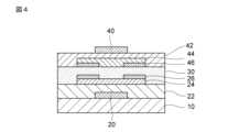
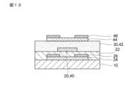
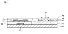
n型トランジスタがボトムゲート・トップコンタクト構造を有する場合、相補型半導体デバイスのp型構造/n型構造は、図1のボトムゲート・トップコンタクト/ボトムゲート・トップコンタクト構造、図2のボトムゲート・ボトムコンタクト/ボトムゲート・トップコンタクト構造、図3のトップゲート・トップコンタクト/ボトムゲート・トップコンタクト構造、または図4のトップゲート・ボトムコンタクト/ボトムゲート・トップコンタクト構造を有することができる。図1を例に説明すると、基板10上にn型構造のゲート電極20、ゲート絶縁層22、n型アモルファス金属酸化物無機半導体層24、及びS/D電極26が配置され、保護層30を挟んで、p型構造のゲート電極40、ゲート絶縁層42、p型有機半導体単結晶層44、及びS/D電極46が配置される。When the n-type transistor has a bottom gate-top contact structure, the p-type structure/n-type structure of the complementary semiconductor device can have the bottom gate-top contact/bottom gate-top contact structure of FIG. 1, the bottom gate-bottom contact/bottom gate-top contact structure of FIG. 2, the top gate-top contact/bottom gate-top contact structure of FIG. 3, or the top gate-bottom contact/bottom gate-top contact structure of FIG. 4. Taking FIG. 1 as an example, an n-
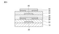
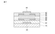
n型トランジスタがボトムゲート・ボトムコンタクト構造を有する場合、相補型半導体デバイスのp型構造/n型構造は、図5のボトムゲート・トップコンタクト/ボトムゲート・ボトムコンタクト構造、図6のボトムゲート・ボトムコンタクト/ボトムゲート・ボトムコンタクト構造、図7のトップゲート・トップコンタクト/ボトムゲート・ボトムコンタクト構造、または図8のトップゲート・ボトムコンタクト/ボトムゲート・ボトムコンタクト構造を有することができる。When the n-type transistor has a bottom-gate-bottom-contact structure, the p-type structure/n-type structure of the complementary semiconductor device can have the bottom-gate-top-contact/bottom-gate-bottom-contact structure of FIG. 5, the bottom-gate-bottom-contact/bottom-gate-bottom-contact structure of FIG. 6, the top-gate-top-contact/bottom-gate-bottom-contact structure of FIG. 7, or the top-gate-bottom-contact/bottom-gate-bottom-contact structure of FIG. 8.
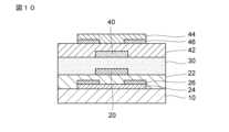
n型トランジスタがトップゲート・トップコンタクト構造を有する場合、相補型半導体デバイスのp型構造/n型構造は、図9のボトムゲート・トップコンタクト/トップゲート・トップコンタクト構造、図10のボトムゲート・ボトムコンタクト/トップゲート・トップコンタクト構造、図11のトップゲート・トップコンタクト/トップゲート・トップコンタクト構造、または図12のトップゲート・ボトムコンタクト/トップゲート・トップコンタクト構造を有することができる。図9の構造のように、n型構造がトップゲート構造及びp型構造がボトムゲート構造を有するとき、n型構造のトップゲート電極とp型構造のボトムゲート電極とを共通にし、且つ保護層とp型ゲート絶縁層とを共通にした図13に示す構造を有してもよい。図10の構造においても同様である。When the n-type transistor has a top gate-top contact structure, the p-type structure/n-type structure of the complementary semiconductor device can have the bottom gate-top contact/top gate-top contact structure of FIG. 9, the bottom gate-bottom contact/top gate-top contact structure of FIG. 10, the top gate-top contact/top gate-top contact structure of FIG. 11, or the top gate-bottom contact/top gate-top contact structure of FIG. 12. When the n-type structure has a top gate structure and the p-type structure has a bottom gate structure, as in the structure of FIG. 9, the top gate electrode of the n-type structure and the bottom gate electrode of the p-type structure may be common, and the protective layer and the p-type gate insulating layer may be common, as shown in FIG. 13. The same applies to the structure of FIG. 10.
n型トランジスタがトップゲート・ボトムコンタクト構造を有する場合、相補型半導体デバイスのp型構造/n型構造は、図14のボトムゲート・トップコンタクト/トップゲート・ボトムコンタクト構造、図15のボトムゲート・ボトムコンタクト/トップゲート・ボトムコンタクト構造、図16のトップゲート・トップコンタクト/トップゲート・ボトムコンタクト構造、または図17のトップゲート・ボトムコンタクト/トップゲート・ボトムコンタクト構造を有することができる。図14及び図15の構造のように、n型構造がトップゲート構造及びp型構造がボトムゲート構造を有するとき、図13と同様に、n型構造のトップゲート電極とp型構造のボトムゲート電極を共通にし、且つ保護層とp型ゲート絶縁層とを共通にした構造を有してもよい。When the n-type transistor has a top gate bottom contact structure, the p-type structure/n-type structure of the complementary semiconductor device can have the bottom gate top contact/top gate bottom contact structure of FIG. 14, the bottom gate bottom contact/top gate bottom contact structure of FIG. 15, the top gate top contact/top gate bottom contact structure of FIG. 16, or the top gate bottom contact/top gate bottom contact structure of FIG. 17. When the n-type structure has a top gate structure and the p-type structure has a bottom gate structure, as in the structures of FIG. 14 and FIG. 15, the top gate electrode of the n-type structure and the bottom gate electrode of the p-type structure may be common, as in FIG. 13, and the protective layer and the p-type gate insulating layer may be common.
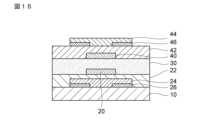
有機半導体単結晶層の主面に垂直方向からみたときに、有機半導体単結晶層がAOS層と重ならないように、有機半導体単結晶層が配置されている場合の相補型半導体デバイスのとり得る例を以下に説明する。Below is a description of possible examples of complementary semiconductor devices in which the organic semiconductor single crystal layer is arranged so that it does not overlap with the AOS layer when viewed from a direction perpendicular to the main surface of the organic semiconductor single crystal layer.
n型トランジスタがボトムゲート・トップコンタクト構造を有する場合、相補型半導体デバイスのn型構造/p型構造は、図18のボトムゲート・トップコンタクト/ボトムゲート・トップコンタクト構造、図19のボトムゲート・トップコンタクト/トップゲート・トップコンタクト構造、図20のボトムゲート・トップコンタクト/ボトムゲート・ボトムコンタクト構造、または図21のボトムゲート・トップコンタクト/トップゲート・ボトムコンタクト構造を有することができる。図18のように、n型構造がトップコンタクト構造及びp型構造がボトムゲート構造を有する場合、n型構造のS/D電極とp型構造のゲート電極とを同一材料で同一層に形成して、保護層とp型ゲート絶縁層とを共通にした図22に示す構造を有してもよい。図20の構造においても同様である。When the n-type transistor has a bottom gate-top contact structure, the n-type structure/p-type structure of the complementary semiconductor device can have the bottom gate-top contact/bottom gate-top contact structure of FIG. 18, the bottom gate-top contact/top gate-top contact structure of FIG. 19, the bottom gate-top contact/bottom gate-bottom contact structure of FIG. 20, or the bottom gate-top contact/top gate-bottom contact structure of FIG. 21. As in FIG. 18, when the n-type structure has a top contact structure and the p-type structure has a bottom gate structure, the S/D electrode of the n-type structure and the gate electrode of the p-type structure may be formed in the same layer with the same material, and the protective layer and the p-type gate insulating layer may be formed in common as shown in FIG. 22. The same applies to the structure of FIG. 20.
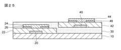
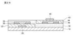
n型トランジスタがボトムゲート・ボトムコンタクト構造を有する場合、相補型半導体デバイスのn型構造/p型構造は、図23のボトムゲート・ボトムコンタクト/ボトムゲート・トップコンタクト構造、図24のボトムゲート・ボトムコンタクト/トップゲート・トップコンタクト構造、図25のボトムゲート・ボトムコンタクト/ボトムゲート・ボトムコンタクト構造、または図26のボトムゲート・ボトムコンタクト/トップゲート・ボトムコンタクト構造を有することができる。When the n-type transistor has a bottom-gate-bottom-contact structure, the n-type structure/p-type structure of the complementary semiconductor device can have the bottom-gate-bottom-contact/bottom-gate-top-contact structure of FIG. 23, the bottom-gate-bottom-contact/top-gate-top-contact structure of FIG. 24, the bottom-gate-bottom-contact/bottom-gate-bottom-contact structure of FIG. 25, or the bottom-gate-bottom-contact/top-gate-bottom-contact structure of FIG. 26.
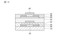
n型トランジスタがトップゲート・トップコンタクト構造を有する場合、相補型半導体デバイスのn型構造/p型構造は、図27のトップゲート・トップコンタクト/ボトムゲート・トップコンタクト構造、図28のトップゲート・トップコンタクト/トップゲート・トップコンタクト構造、図29のトップゲート・トップコンタクト/ボトムゲート・ボトムコンタクト構造、または図30のトップゲート・トップコンタクト/トップゲート・ボトムコンタクト構造を有することができる。図27のようにn型構造がトップゲート構造及びp型構造がボトムゲート構造を有する場合、n型構造のゲートとp型構造のゲート電極とを同一材料で同一層に形成して、保護層とp型ゲート絶縁層とを共通にした図31に示す構造を有してもよい。図29の構造においても同様である。When the n-type transistor has a top gate-top contact structure, the n-type structure/p-type structure of the complementary semiconductor device can have the top gate-top contact/bottom gate-top contact structure of FIG. 27, the top gate-top contact/top gate-top contact structure of FIG. 28, the top gate-top contact/bottom gate-bottom contact structure of FIG. 29, or the top gate-top contact/top gate-bottom contact structure of FIG. 30. When the n-type structure has a top gate structure and the p-type structure has a bottom gate structure as in FIG. 27, the gate of the n-type structure and the gate electrode of the p-type structure may be formed in the same layer with the same material, and the protective layer and the p-type gate insulating layer may be formed in common as shown in FIG. 31. The same applies to the structure in FIG. 29.
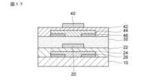
n型トランジスタがトップゲート・ボトムコンタクト構造を有する場合、相補型半導体デバイスのn型構造/p型構造は、図32のトップゲート・ボトムコンタクト/ボトムゲート・トップコンタクト構造、図33のトップゲート・ボトムコンタクト/トップゲート・トップコンタクト構造、図34のトップゲート・ボトムコンタクト/ボトムゲート・ボトムコンタクト構造、または図35のトップゲート・ボトムコンタクト/トップゲート・ボトムコンタクト構造を有することができる。図32のようにn型構造がトップゲート構造及びp型構造がボトムゲート構造を有する場合、図31と同様に、保護層とp型構造のゲート絶縁層とを共通にした構造を有してもよい。図33の構造においても同様である。When the n-type transistor has a top gate bottom contact structure, the n-type structure/p-type structure of the complementary semiconductor device can have the top gate bottom contact/bottom gate top contact structure of FIG. 32, the top gate bottom contact/top gate top contact structure of FIG. 33, the top gate bottom contact/bottom gate bottom contact structure of FIG. 34, or the top gate bottom contact/top gate bottom contact structure of FIG. 35. When the n-type structure has a top gate structure and the p-type structure has a bottom gate structure as in FIG. 32, the protective layer and the gate insulating layer of the p-type structure may be in common, as in FIG. 31. The same applies to the structure in FIG. 33.
図1~図35に示すように、AOS層は、基板上、ゲート絶縁層上、ゲート電極上、S/D電極上、またはそれらの組み合わせの上に形成され得る。AOS層上には、保護層、S/D電極、ゲート絶縁層、ゲート電極、有機半導体単結晶層、またはそれらの組み合わせが隣接して形成され得る。As shown in Figures 1 to 35, the AOS layer may be formed on a substrate, a gate insulating layer, a gate electrode, an S/D electrode, or a combination thereof. A protective layer, an S/D electrode, a gate insulating layer, a gate electrode, an organic semiconductor single crystal layer, or a combination thereof may be formed adjacent to the AOS layer.
本開示の方法は、基板を用意すること、前記基板上にn型構造を形成すること、前記n型構造上に保護層を形成すること、及び前記保護層上にp型構造を形成することを含む、無機/有機ハイブリッド相補型半導体デバイスの製造方法であって、前記n型構造を形成することが、ゾルゲル法を用いて、金属塩を含むn型アモルファス金属酸化物無機半導体の前駆体溶液を調製すること、前記基板上に、前記前駆体溶液を塗布して前駆体膜を形成すること、及び前記前駆体膜を350~400℃で熱処理してn型アモルファス金属酸化物無機半導体層を形成することを含み、前記p型構造を形成することが、塗布法を用いてp型有機半導体単結晶層を形成することを含み、前記p型有機半導体単結晶層の主面に垂直方向からみたときに、前記p型有機半導体単結晶層の少なくとも一部が前記n型アモルファス金属酸化物無機半導体層に重なるように、または前記p型有機半導体単結晶層が前記n型アモルファス金属酸化物無機半導体層と重ならないように、前記p型有機半導体単結晶層が配置されており、前記p型有機半導体単結晶層と前記n型アモルファス金属酸化物無機半導体層との間の距離が1mm以下であり、前記n型アモルファス金属酸化物無機半導体層が、前記基板側よりも前記p型有機半導体単結晶層側の酸素欠陥量が多い、厚み方向の酸素欠陥量の分布を有する、無機/有機ハイブリッド相補型半導体デバイスの製造方法を対象とする。n型構造及びp型構造はそれぞれ、図1~図35を参照して説明したn型構造及びp型構造の上記例示の構成をとり得る。The method disclosed herein is a method for manufacturing an inorganic/organic hybrid complementary semiconductor device, comprising: preparing a substrate; forming an n-type structure on the substrate; forming a protective layer on the n-type structure; and forming a p-type structure on the protective layer, wherein forming the n-type structure comprises using a sol-gel method to prepare a precursor solution of an n-type amorphous metal oxide inorganic semiconductor containing a metal salt, applying the precursor solution onto the substrate to form a precursor film, and heat-treating the precursor film at 350 to 400°C to form an n-type amorphous metal oxide inorganic semiconductor layer, and forming the p-type structure comprises using a coating method to form a p-type organic semiconductor single crystal layer, and forming the p-type structure comprises using a coating method to form a p-type organic semiconductor single crystal layer. The present invention relates to a method for manufacturing an inorganic/organic hybrid complementary semiconductor device, in which the p-type organic semiconductor single crystal layer is arranged so that at least a portion of the p-type organic semiconductor single crystal layer overlaps the n-type amorphous metal oxide inorganic semiconductor layer or the p-type organic semiconductor single crystal layer does not overlap the n-type amorphous metal oxide inorganic semiconductor layer when viewed from a direction perpendicular to the main surface of the p-type organic semiconductor single crystal layer, the distance between the p-type organic semiconductor single crystal layer and the n-type amorphous metal oxide inorganic semiconductor layer is 1 mm or less, and the n-type amorphous metal oxide inorganic semiconductor layer has a distribution of oxygen defects in the thickness direction in which the amount of oxygen defects is greater on the p-type organic semiconductor single crystal layer side than on the substrate side. The n-type structure and the p-type structure can have the above-mentioned exemplary configurations of the n-type structure and the p-type structure described with reference to Figures 1 to 35, respectively.
本開示の方法では、アモルファス金属酸化物無機半導体層(AOS層)及び有機半導体単結晶層の成膜プロセスとして溶液プロセスを用いる。AOS層及び有機半導体単結晶層を、溶液プロセスを用いて大気下で成膜することができるので、ドライプロセスで用いられる高真空チャンバー等の特別な装置が不要であり、安価に製造することができる。特に、大面積化を図る場合に、高真空チャンバー等の特別な装置の大型化が不要であり、ドライプロセスに対してコスト低減効果がさらに大きくなる。In the method disclosed herein, a solution process is used as a deposition process for the amorphous metal oxide inorganic semiconductor layer (AOS layer) and the organic semiconductor single crystal layer. Since the AOS layer and the organic semiconductor single crystal layer can be deposited in air using a solution process, special equipment such as a high vacuum chamber used in a dry process is not required, and they can be manufactured at low cost. In particular, when attempting to increase the area, there is no need to enlarge special equipment such as a high vacuum chamber, and the cost reduction effect is even greater compared to the dry process.
AOS層の成膜プロセスとして、まず、図36に示すように、ゾルゲル法を用いてAOSの前駆体溶液を調製する。金属塩を水または有機溶媒中に溶解した後、加水分解し、縮合してM-O-M構造を形成して前駆体をゾル化させた前駆体溶液を調製する。例えば、AOS層としてIZO層を形成する場合、硝酸インジウムと硝酸亜鉛とを混合して前駆体溶液を調製する。図36におけるMは、AOS中に含まれる金属カチオン元素であり、例えばIn、Zn、Ga、Al、Sn、Y等の金属元素が挙げられる。Rはアルキル基である。Xとしては、塩化物塩、硝酸塩、酢酸塩等が挙げられる。溶媒は、水、水溶液、アルコール等の、酸素が金属イオンに結合・架橋可能な溶媒であることができ、O及びHを含み、Cを含んでもよく、さらにN、F、Cl等の他の元素を含んでもよい。溶媒は、例えば2-メトキシエタノールであることができるAs a process for forming the AOS layer, first, as shown in FIG. 36, a precursor solution of AOS is prepared using a sol-gel method. A metal salt is dissolved in water or an organic solvent, and then hydrolyzed and condensed to form an M-O-M structure, and the precursor is solvated to prepare a precursor solution. For example, when an IZO layer is formed as the AOS layer, a precursor solution is prepared by mixing indium nitrate and zinc nitrate. M in FIG. 36 is a metal cation element contained in the AOS, and examples of the metal elements include In, Zn, Ga, Al, Sn, and Y. R is an alkyl group. Examples of X include chloride salts, nitrate salts, and acetate salts. The solvent can be a solvent in which oxygen can bond to and crosslink with metal ions, such as water, an aqueous solution, or an alcohol, and contains O and H, and may also contain C, and may further contain other elements such as N, F, and Cl. The solvent can be, for example, 2-methoxyethanol.
次いで、前駆体溶液を基板上に塗布して前駆体の薄膜を形成する。前駆体溶液の塗布方法は、好ましくは、スピンコート法、バーコート法、スプレーコート法、ディップコート法、インクジェット法、フレキソ印刷法、またはグラビア印刷法であり、より好ましくはスピンコート法、バーコート法、スプレーコート法、ディップコート法、またはインクジェット法であり、さらに好ましくはスピンコート法である。図37に、前駆体溶液を基板上にスピンコート位して前駆体の薄膜を形成する態様を表す模式図を示す。前駆体の薄膜をソフトベーク(熱処理)して溶媒を除去し、ハードベーク(熱処理)して緻密なアモルファス金属酸化物無機半導体層を形成することができる。The precursor solution is then applied onto the substrate to form a thin precursor film. The method for applying the precursor solution is preferably spin coating, bar coating, spray coating, dip coating, inkjet printing, flexographic printing, or gravure printing, more preferably spin coating, bar coating, spray coating, dip coating, or inkjet printing, and even more preferably spin coating. Figure 37 shows a schematic diagram illustrating an embodiment in which the precursor solution is spin-coated onto the substrate to form a thin precursor film. The thin precursor film can be soft-baked (heat-treated) to remove the solvent, and then hard-baked (heat-treated) to form a dense amorphous metal oxide inorganic semiconductor layer.
スピンコート法は、活性層の堆積において、再現性の良さと、加工されたままの膜の均一性の高さにおいて利点を有する。スピンコート法で形成した熱処理前の薄膜は、前駆体溶液の調製で用いられる窒素等の不純物を多量に含んでおり、ドライプロセスで得られるものとは全く異なるが、熱処理によって窒素等の不純物はガスとして放出され、不純物が抜けた箇所が酸素で架橋され得る。The spin coating method has the advantage of good reproducibility in the deposition of active layers and high uniformity of the processed film. The thin film formed by the spin coating method before heat treatment contains a large amount of impurities such as nitrogen used in the preparation of the precursor solution, and is completely different from that obtained by the dry process. However, the nitrogen and other impurities are released as gas by heat treatment, and the areas where the impurities have disappeared can be bridged with oxygen.
溶媒を除去するソフトベークは、好ましくは100~150℃で行う。前記好ましい温度で熱処理することにより、より良好に溶媒を除去することができる。The soft bake to remove the solvent is preferably performed at 100 to 150°C. By performing heat treatment at the preferred temperature, the solvent can be removed more effectively.
焼成するハードベークは350~400℃で行われる。400℃以下という低温で熱処理することにより、フレキシブル基板を含む場合でも、フレキシブル基板を損傷させずに、アモルファス金属酸化物無機半導体層を形成することができる。また、熱処理温度が高いとM-O-M構造の形成が容易になり、結晶性が高くなり、浅いドナー濃度が増加し、移動度が向上するが、温度が高すぎるとオン電圧(VON)の負電圧シフトや高オフ電流が発生し、消費電力が増加する傾向があるため、この観点でも熱処理温度は400℃以下とする。熱処理温度が350℃未満の場合は、アモルファス金属酸化物無機半導体層中に有機残渣が発生し、有機残渣は電子トラップとして働くため、熱処理温度は350℃以上とする。 The hard bake is performed at 350 to 400° C. By performing the heat treatment at a low temperature of 400° C. or less, an amorphous metal oxide inorganic semiconductor layer can be formed without damaging the flexible substrate, even when the flexible substrate is included. In addition, when the heat treatment temperature is high, the formation of the M-O-M structure becomes easier, the crystallinity becomes high, the shallow donor concentration increases, and the mobility improves. However, when the temperature is too high, a negative voltage shift of the on-voltage (VON ) and a high off-current occur, and power consumption tends to increase. From this viewpoint, the heat treatment temperature is set to 400° C. or less. When the heat treatment temperature is less than 350° C., organic residues are generated in the amorphous metal oxide inorganic semiconductor layer, and the organic residues act as electron traps, so the heat treatment temperature is set to 350° C. or more.
熱処理温度の下限は、好ましくは355℃以上、より好ましくは360℃以上、さらに好ましくは365℃以上である。熱処理温度の上限は、好ましくは400℃未満、より好ましくは395℃以下、さらにより好ましくは390℃以下、さらにより好ましくは385℃以下、さらにより好ましくは380℃以下、さらにより好ましくは375℃以下である。上記好ましい温度範囲で熱処理することにより、消費電力及び有機残渣をより低減することができる。The lower limit of the heat treatment temperature is preferably 355°C or higher, more preferably 360°C or higher, and even more preferably 365°C or higher. The upper limit of the heat treatment temperature is preferably less than 400°C, more preferably 395°C or lower, even more preferably 390°C or lower, even more preferably 385°C or lower, even more preferably 380°C or lower, and even more preferably 375°C or lower. By performing heat treatment within the above preferred temperature range, power consumption and organic residues can be further reduced.
本方法で形成されるAOS層の面積は、好ましくは2mm2以上、より好ましくは10mm2以上、さらに好ましくは100mm2以上、さらにより好ましくは1000mm2以上、さらにより好ましくは10000mm2以上である。AOS層の面積の上限は、特に限定されず、製造設備の大きさによって制限され、例えば10m2としてもよい。本開示の相補型半導体デバイスにおけるAOS層は、溶液プロセスで成膜するため、低コストで上記のように大きな面積を有することができる。 The area of the AOS layer formed by this method is preferably2 mm2 or more, more preferably 10mm2 or more, even more preferably 100mm2 or more, even more preferably 1000mm2 or more, and even more preferably 10000mm2 or more. The upper limit of the area of the AOS layer is not particularly limited and is limited by the size of the manufacturing equipment, and may be, for example, 10m2 . The AOS layer in the complementary semiconductor device of the present disclosure is formed by a solution process, and therefore can have such a large area at low cost.
(AOS層のパターニング)
溶液プロセスで成膜するAOS層は、光ラジカル開始剤と炭酸ナトリウム現像剤とを用いてパターニングを行うことが好ましい。図38に、光ラジカル開始剤と炭酸ナトリウム現像剤を用いたパターニング操作を表す模式図を示す。 (Patterning of AOS layer)
The solution-processed AOS layer is preferably patterned using a photoradical initiator and a sodium carbonate developer. A schematic diagram illustrating the patterning operation using a photoradical initiator and a sodium carbonate developer is shown in Figure 38.
溶液プロセスで成膜するAOS層は、酸素、水、有機溶媒等の外部環境に非常に敏感である。従来のフォトリソグラフィプロセスで用いられる光酸発生剤や水酸化テトラメチルアンモニウム(TMAH)等の強アルカリ現像剤は、AOS層にダメージを与え得る。これに対して、光ラジカル開始剤と、強アルカリ現像剤よりもマイルドな溶媒である炭酸ナトリウム現像剤(1質量%のNa2CO3溶液)とを用いてフォトリソグラフィ法でパターニングすることにより、溶液プロセスで成膜したAOS層の特性を変えずに、微細なパターニングを行うことができる。 The AOS layer formed by the solution process is very sensitive to external environments such as oxygen, water, and organic solvents. The photoacid generator and strong alkaline developer such as tetramethylammonium hydroxide (TMAH) used in conventional photolithography processes can damage the AOS layer. In contrast, by patterning by photolithography using a photoradical initiator and a sodium carbonate developer (1% bymassNa2CO3 solution), which is a milder solvent than the strong alkaline developer, fine patterning can be performed without changing the properties of the AOS layer formed by the solution process.
図39に示すように、シャドウマスクを介してS/D電極を構成する金属を蒸着して、AOS層上にS/D電極を形成することができる。S/D電極のパターニングには、レジストPDMを使用してもよい。S/D電極を構成する金属は、例えばAl等が挙げられる。As shown in FIG. 39, the metal constituting the S/D electrode can be evaporated through a shadow mask to form the S/D electrode on the AOS layer. Resist PDM may be used to pattern the S/D electrode. Examples of metals constituting the S/D electrode include Al.
図40に、S/D電極を形成したAOS(MOSともいう)層を含むn型TFTの一例の模式図を示す。Figure 40 shows a schematic diagram of an example of an n-type TFT that includes an AOS (also called MOS) layer on which S/D electrodes are formed.
好ましくは、保護層を形成することが、ポリマーが溶解した有機溶媒を調製すること、n型構造上に、ポリマーが溶解した有機溶媒を塗布して第1の有機膜を形成すること、及び第1の有機膜上に、化学気相成長法を用いて真空蒸着膜である第2の有機膜を形成することを含む。Preferably, forming the protective layer includes preparing an organic solvent in which a polymer is dissolved, applying the organic solvent in which the polymer is dissolved onto the n-type structure to form a first organic film, and forming a second organic film, which is a vacuum deposition film, on the first organic film by using a chemical vapor deposition method.
有機溶媒とポリマーを混合して、ポリマーが溶解した有機溶媒を調製することができる。ポリマーの濃度は、第1の有機膜の目的とする厚みに応じて変えればよく、例えば1~80mg/mL、2~70mg/mL、または3~60mg/mLである。The organic solvent and the polymer can be mixed to prepare an organic solvent in which the polymer is dissolved. The concentration of the polymer can be varied depending on the desired thickness of the first organic film, and is, for example, 1 to 80 mg/mL, 2 to 70 mg/mL, or 3 to 60 mg/mL.
n型構造上に、ポリマーが溶解した有機溶媒を塗布して第1の有機膜を形成する。塗布方法は、好ましくは、スピンコート法、バーコート法、スプレーコート法、ディップコート法、インクジェット法、フレキソ印刷法、またはグラビア印刷法であり、より好ましくはスピンコート法、バーコート法、スプレーコート法、ディップコート法、またはインクジェット法であり、さらに好ましくはスピンコート法である。The first organic film is formed by applying an organic solvent in which a polymer is dissolved onto the n-type structure. The application method is preferably a spin coating method, a bar coating method, a spray coating method, a dip coating method, an inkjet method, a flexographic printing method, or a gravure printing method, more preferably a spin coating method, a bar coating method, a spray coating method, a dip coating method, or an inkjet method, and even more preferably a spin coating method.
第1の有機膜上に、化学気相成長法(CVD)を用いて真空蒸着膜である第2の有機膜を形成する。真空蒸着膜である第2の有機膜は、CVDで成膜する。CVDは軽い真空プロセスであり、成膜速度、処理面積、緻密性、及び均一性の点で好ましい。A second organic film, which is a vacuum deposition film, is formed on the first organic film using chemical vapor deposition (CVD). The second organic film, which is a vacuum deposition film, is formed by CVD. CVD is a light vacuum process, and is preferable in terms of film formation speed, processing area, density, and uniformity.
有機半導体単結晶層は、有機半導体単結晶層は、ゲート絶縁層、S/D電極、保護層、またはそれらの組み合わせ上に、直接、塗布法を用いて成膜してもよい。The organic semiconductor single crystal layer may be formed directly on the gate insulating layer, the S/D electrode, the protective layer, or a combination thereof by using a coating method.
塗布法は、有機半導体を有機溶媒に溶解させて有機半導体溶液を調製し、基板上に有機半導体溶液を塗布し、有機溶媒を蒸発させて膜を形成する方法である。有機溶媒としては、従来、塗布法に用いられている有機溶媒を用いることができ、例えばトルエン、ジクロロベンゼン等を用いることができる。The coating method involves dissolving an organic semiconductor in an organic solvent to prepare an organic semiconductor solution, coating the organic semiconductor solution on a substrate, and evaporating the organic solvent to form a film. As the organic solvent, any organic solvent that has been conventionally used in coating methods can be used, such as toluene or dichlorobenzene.
塗布法で形成される有機半導体単結晶層の面積は、好ましくは2mm2以上、より好ましくは10mm2以上、さらに好ましくは100mm2以上、さらにより好ましくは1000mm2以上、さらにより好ましくは10000mm2以上である。有機半導体単結晶層の面積の上限は、特に限定されず、製造設備の大きさによって制限され、例えば10m2としてもよい。従来、気相成長法を用いる場合は最大でも1mm2程度の面積を有する有機半導体単結晶膜しか得られなかったのに対して、本方法における有機半導体単結晶層は、溶液プロセスで成膜するため、上記のように大きな面積を有することができる。 The area of the organic semiconductor single crystal layer formed by the coating method is preferably 2 mm2 or more, more preferably 10 mm2 or more, even more preferably 100 mm2 or more, even more preferably 1000 mm2 or more, and even more preferably 10000 mm2 or more. The upper limit of the area of the organic semiconductor single crystal layer is not particularly limited, and is limited by the size of the manufacturing equipment, and may be, for example, 10 m2. Conventionally, when using a vapor phase growth method, only an organic semiconductor single crystal film having an area of about 1 mm2 at most could be obtained, whereas the organic semiconductor single crystal layer in this method can have a large area as described above because it is formed by a solution process.
好ましくは、p型有機半導体単結晶層を形成することが、塗布法を用いて、親水性且つ非水溶性の第1の基板上に、p型有機半導体単結晶膜を形成すること、及び第1の基板とp型有機半導体単結晶膜との界面に水または水溶液を適用して、p型有機半導体単結晶膜を第1の基板から分離させて、第2の基板上にp型有機半導体単結晶層を配置することを含み、第2の基板は、n型構造のゲート絶縁層及びS/D電極のうちの少なくとも1つ、保護層、またはそれらの組み合わせである。Preferably, forming the p-type organic semiconductor single crystal layer includes forming a p-type organic semiconductor single crystal film on a hydrophilic and water-insoluble first substrate using a coating method, and applying water or an aqueous solution to the interface between the first substrate and the p-type organic semiconductor single crystal film to separate the p-type organic semiconductor single crystal film from the first substrate and disposing the p-type organic semiconductor single crystal layer on a second substrate, the second substrate being at least one of a gate insulating layer and an S/D electrode of an n-type structure, a protective layer, or a combination thereof.
第1の基板から分離させるp型有機半導体単結晶膜を、上記ゲート絶縁層、S/D電極、保護層、またはそれらの組み合わせの上に配置して有機半導体単結晶層を形成する。n型構造のゲート絶縁層及びS/D電極のうちの少なくとも1つ、保護層、またはそれらの組み合わせを第2の基板という。第2の基板とは、p型有機半導体単結晶層を配置するときにp型有機半導体単結晶層に接する表面に位置するものをいう。この有機半導体単結晶層の形成方法によれば、第2の基板が、疎水性、溶剤可溶性、非耐熱性、またはそれらの組み合わせの特性を有していても、さらには、凹部、凸部、または凹凸部を有していても、第2の基板上に、薄い膜厚を有する有機半導体単結晶層を容易に配置することができる。The p-type organic semiconductor single crystal film to be separated from the first substrate is disposed on the gate insulating layer, the S/D electrode, the protective layer, or a combination thereof to form an organic semiconductor single crystal layer. At least one of the gate insulating layer and the S/D electrode of the n-type structure, the protective layer, or a combination thereof is called the second substrate. The second substrate refers to a substrate located on the surface that contacts the p-type organic semiconductor single crystal layer when the p-type organic semiconductor single crystal layer is disposed. According to this method for forming an organic semiconductor single crystal layer, even if the second substrate has characteristics of hydrophobicity, solvent solubility, non-heat resistance, or a combination thereof, and further, even if the second substrate has a concave portion, a convex portion, or an uneven portion, an organic semiconductor single crystal layer having a thin film thickness can be easily disposed on the second substrate.
塗布法として、従来から用いられている方法を用いることができ、例えば、エッジキャスト法、連続エッジキャスト法、ドロップキャスト法、スピンコーティング法、印刷法(インクジェット法やグラビア印刷法)、ディスペンサー法、及びスプレー法、ディップコート法、ダイコーター法、ロールコーター法、バーコーター法、ブレードコーティング法等を用いることができる。As the coating method, a method that has been conventionally used can be used, such as edge casting, continuous edge casting, drop casting, spin coating, printing (inkjet printing or gravure printing), dispenser, spray, dip coating, die coater, roll coater, bar coater, blade coating, etc.
第1の基板は、水の接触角が好ましくは20度以下、より好ましくは10度以下の親水性基板である。第1の基板は非水溶性であり、例えば雲母またはガラスであることができる。第1の基板が非水溶性であるため、第1の基板と有機半導体単結晶膜との界面に水または水溶液を適用する際に、第1の基板の成分が溶出して有機半導体単結晶膜に付着したり反応することがなく、高純度な有機半導体単結晶膜を得ることができる。また、第1の基板と有機半導体単結晶膜との界面に水または水溶液を適用する際に、第1の基板の形状が崩れることなく維持されるために、有機半導体単結晶膜の形状を歪ませることなく第1の基板から有機半導体単結晶膜を分離させることができる。非水溶性とは、水または水溶液に実質的に溶解、分解、または膨潤しないことをいう。ガラスは、好ましくは、表面にUV・オゾン処理または親水性コーティング材料等により親水化処理されたものである。The first substrate is a hydrophilic substrate having a contact angle with water of preferably 20 degrees or less, more preferably 10 degrees or less. The first substrate is water-insoluble, and can be, for example, mica or glass. Since the first substrate is water-insoluble, when water or an aqueous solution is applied to the interface between the first substrate and the organic semiconductor single crystal film, the components of the first substrate do not dissolve and adhere to or react with the organic semiconductor single crystal film, and a high-purity organic semiconductor single crystal film can be obtained. Furthermore, when water or an aqueous solution is applied to the interface between the first substrate and the organic semiconductor single crystal film, the shape of the first substrate is maintained without being distorted, and the organic semiconductor single crystal film can be separated from the first substrate without distorting the shape of the organic semiconductor single crystal film. Water-insoluble means that the glass does not substantially dissolve, decompose, or swell in water or an aqueous solution. The glass is preferably hydrophilized by UV/ozone treatment or a hydrophilic coating material or the like.
第1の基板と有機半導体単結晶膜との界面に水または水溶液を適用して、有機半導体単結晶膜を第1の基板から分離させる。第1の基板上に塗布する有機半導体単結晶膜の分子は疎水性であるため、親水性の第1の基板と疎水性の有機半導体単結晶膜の分子との間に水または水溶液が入り、有機半導体単結晶膜を第1の基板から分離させることができる。Water or an aqueous solution is applied to the interface between the first substrate and the organic semiconductor single crystal film, and the organic semiconductor single crystal film is separated from the first substrate. Since the molecules of the organic semiconductor single crystal film applied to the first substrate are hydrophobic, water or an aqueous solution enters between the hydrophilic first substrate and the molecules of the hydrophobic organic semiconductor single crystal film, and the organic semiconductor single crystal film can be separated from the first substrate.
親水性の第1の基板の水または水溶液の接触角は、疎水性の有機半導体単結晶膜の水または水溶液の接触角よりも小さく、第1の基板と有機半導体単結晶膜との水または水溶液の接触角の差は、好ましくは80度以上、より好ましくは90度以上である。有機半導体単結晶膜の接触角は好ましくは100~120度である。親水性の第1の基板と疎水性の有機半導体単結晶膜との接触角の差が、前記好ましい範囲であることにより、より安定して第1の基板から有機半導体単結晶膜を剥離させることができる。The contact angle of water or an aqueous solution of the hydrophilic first substrate is smaller than the contact angle of water or an aqueous solution of the hydrophobic organic semiconductor single crystal film, and the difference in the contact angle of water or an aqueous solution between the first substrate and the organic semiconductor single crystal film is preferably 80 degrees or more, more preferably 90 degrees or more. The contact angle of the organic semiconductor single crystal film is preferably 100 to 120 degrees. By having the difference in contact angle between the hydrophilic first substrate and the hydrophobic organic semiconductor single crystal film within the above-mentioned preferred range, the organic semiconductor single crystal film can be peeled off from the first substrate more stably.
第1の基板と有機半導体単結晶膜との界面に水または水溶液を適用する方法は特に限定されず、有機半導体単結晶膜を形成した第1の基板を水または水溶液中に浸漬すること、第1の基板と有機半導体単結晶膜との界面にスポイトで滴下する等の方法であることができる。The method of applying water or an aqueous solution to the interface between the first substrate and the organic semiconductor single crystal film is not particularly limited, and may be, for example, immersing the first substrate on which the organic semiconductor single crystal film is formed in water or an aqueous solution, or dropping the solution onto the interface between the first substrate and the organic semiconductor single crystal film with a dropper.
第1の基板と有機半導体単結晶膜との界面に水または水溶液を適用する方法は、好ましくは、有機半導体単結晶膜を形成した第1の基板を水または水溶液中に浸漬することを含む。有機半導体単結晶膜を形成した第1の基板を水または水溶液中に浸漬することによって、水または水溶液中で有機半導体単結晶膜が第1の基板から分離し、水または水溶液中で自立した(self-standing状態の)有機半導体単結晶膜を得ることができる。自立した有機半導体単結晶膜は、上記第2の基板上に配置することができる。The method of applying water or an aqueous solution to the interface between the first substrate and the organic semiconductor single crystal film preferably includes immersing the first substrate on which the organic semiconductor single crystal film is formed in water or an aqueous solution. By immersing the first substrate on which the organic semiconductor single crystal film is formed in water or an aqueous solution, the organic semiconductor single crystal film separates from the first substrate in the water or aqueous solution, and an organic semiconductor single crystal film that is free-standing (self-standing) in the water or aqueous solution can be obtained. The free-standing organic semiconductor single crystal film can be disposed on the second substrate.
有機半導体単結晶膜を第2の基板の上に配置することは、好ましくは、第1の基板上に形成した有機半導体単結晶膜に接するように第2の基板を配置しながら、第1の基板と有機半導体単結晶膜との界面に水または水溶液を適用して有機半導体単結晶膜を第1の基板から分離させて第2の基板の上に配置することを含む。このように有機半導体単結晶膜に接するように第2の基板を配置しながら有機半導体単結晶膜を第1の基板から分離させることにより、第1の基板から第2の基板の上に、有機半導体単結晶膜を移し替えることができる。Placing the organic semiconductor single crystal film on the second substrate preferably includes applying water or an aqueous solution to the interface between the first substrate and the organic semiconductor single crystal film while placing the second substrate so as to be in contact with the organic semiconductor single crystal film formed on the first substrate, thereby separating the organic semiconductor single crystal film from the first substrate and placing the organic semiconductor single crystal film on the second substrate. By separating the organic semiconductor single crystal film from the first substrate while placing the second substrate so as to be in contact with the organic semiconductor single crystal film in this manner, the organic semiconductor single crystal film can be transferred from the first substrate onto the second substrate.
別法では、有機半導体単結晶膜を第2の基板の上に配置することは、好ましくは、有機半導体単結晶膜を形成した第1の基板を水または水溶液中に浸漬し、水または水溶液中で有機半導体単結晶膜を第1の基板から分離して自立した有機半導体単結晶膜を得て、水または水溶液中で第2の基板の上に有機半導体単結晶膜を配置することを含む。このように、水または水溶液中で、自立した有機半導体単結晶膜を第2の基板の上に配置することによって、第1の基板から第2の基板の上に容易に有機半導体単結晶膜を移し替えることができる。Alternatively, disposing the organic semiconductor single crystal film on the second substrate preferably includes immersing the first substrate on which the organic semiconductor single crystal film is formed in water or an aqueous solution, separating the organic semiconductor single crystal film from the first substrate in the water or aqueous solution to obtain a free-standing organic semiconductor single crystal film, and disposing the organic semiconductor single crystal film on the second substrate in the water or aqueous solution. In this way, by disposing the free-standing organic semiconductor single crystal film on the second substrate in the water or aqueous solution, the organic semiconductor single crystal film can be easily transferred from the first substrate to the second substrate.
さらに好ましくは、有機半導体単結晶膜を第2の基板の上に配置することは、第1の基板上に形成した有機半導体単結晶膜に接するように第2の基板を配置しながら、第1の基板、有機半導体単結晶膜、及び第2の基板を水または水溶液中に浸漬し、有機半導体単結晶膜を第1の基板から第2の基板に移し替えることを含む。このように、水または水溶液中で、有機半導体単結晶膜に接するように第2の基板を配置しながら有機半導体単結晶膜を第1の基板から分離させることにより、第1の基板から第2の基板の上にさらに容易に有機半導体単結晶膜を移し替えることができる。More preferably, disposing the organic semiconductor single crystal film on the second substrate includes immersing the first substrate, the organic semiconductor single crystal film, and the second substrate in water or an aqueous solution while disposing the second substrate so as to be in contact with the organic semiconductor single crystal film formed on the first substrate, and transferring the organic semiconductor single crystal film from the first substrate to the second substrate. In this way, by separating the organic semiconductor single crystal film from the first substrate while disposing the second substrate so as to be in contact with the organic semiconductor single crystal film in water or an aqueous solution, the organic semiconductor single crystal film can be more easily transferred from the first substrate to the second substrate.
有機半導体単結晶膜のパターニングは、特に限定されず従来の方法で行うことができるが、ドライフィルムのフォトレジストを用いて行うことが好ましい。ドライフィルムのフォトレジストを用いる場合、有機溶媒を含む塗布するタイプのフォトレジストを用いる場合よりも、有機半導体単結晶膜のダメージを抑制することができる。Patterning of the organic semiconductor single crystal film is not particularly limited and can be performed by a conventional method, but is preferably performed using a dry film photoresist. When a dry film photoresist is used, damage to the organic semiconductor single crystal film can be suppressed more than when a coat-type photoresist containing an organic solvent is used.
好ましくは、p型有機半導体単結晶層を形成することが、塗布法を用いて、親水性且つ非水溶性の第3の基板上に、p型有機半導体単結晶膜を形成すること、p型有機半導体単結晶膜を、凸部及び凹部を有するスタンプの前記凸部に押し付けること、第3の基板と前記p型有機半導体単結晶膜との界面に水または水溶液を適用して、凸部にp型有機半導体単結晶膜を転写すること、及び凸部に転写されたp型有機半導体単結晶膜を第4の基板に押し付けて、第4の基板に前記p型有機半導体単結晶膜を転写してパターニングされたp型有機半導体単結晶層を得ることを含み、第4の基板は、n型構造のゲート絶縁層及びS/D電極のうちの少なくとも1つ、保護層、またはそれらの組み合わせである。Preferably, forming a p-type organic semiconductor single crystal layer includes forming a p-type organic semiconductor single crystal film on a hydrophilic and water-insoluble third substrate using a coating method, pressing the p-type organic semiconductor single crystal film onto the convex parts of a stamp having convex parts and concave parts, applying water or an aqueous solution to the interface between the third substrate and the p-type organic semiconductor single crystal film to transfer the p-type organic semiconductor single crystal film onto the convex parts, and pressing the p-type organic semiconductor single crystal film transferred onto the convex parts onto a fourth substrate to transfer the p-type organic semiconductor single crystal film onto the fourth substrate to obtain a patterned p-type organic semiconductor single crystal layer, the fourth substrate being at least one of an n-type gate insulating layer and an S/D electrode, a protective layer, or a combination thereof.
n型構造のゲート絶縁層及びS/D電極のうちの少なくとも1つ、保護層、またはそれらの組み合わせを第4の基板という。第4の基板とは、スタンプと凸部からp型有機半導体単結晶層を転写してパターニングするときにp型有機半導体単結晶層に接する表面に位置するものをいう。At least one of the gate insulating layer and S/D electrodes of the n-type structure, the protective layer, or a combination of them is called the fourth substrate. The fourth substrate refers to the surface that is in contact with the p-type organic semiconductor single crystal layer when the p-type organic semiconductor single crystal layer is transferred and patterned from the stamp and the protrusions.
この方法によれば、モールドを作製しておけばフォトリソグラフィが不要で低コストである。スタンプへの転写と同時にp型有機半導体単結晶層のパターニングを行うことができるため、パターニングを短時間で行うことができる。スタンプの凹凸を利用してp型有機半導体単結晶層のパターニングを物理的に行うので、溶剤やレーザーを用いる必要がなく、様々なp型有機半導体単結晶層のパターニングを行うことができ、汎用性が高い。第4の基板にはスタンプを押し付けるだけであるため、第4の基板に溶媒等のダメージを与えることがない。例えば、第4の基板が有機材料を溶解させる溶剤に溶解性である場合でも、パターニングされたp型有機半導体単結晶層を形成することができる。スタンプには水または水溶液しか触れず、溶媒の接触や加熱される必要がないため、溶媒や熱によるスタンプの膨潤または収縮がない。例えば、あらかじめ塗布して単結晶となった膜をパターニングできる。According to this method, photolithography is unnecessary if a mold is prepared, and the cost is low. Since the p-type organic semiconductor single crystal layer can be patterned simultaneously with the transfer onto the stamp, patterning can be performed in a short time. Since the p-type organic semiconductor single crystal layer is physically patterned using the unevenness of the stamp, there is no need to use a solvent or laser, and various p-type organic semiconductor single crystal layers can be patterned, making it highly versatile. Since the stamp is simply pressed against the fourth substrate, the fourth substrate is not damaged by a solvent or the like. For example, even if the fourth substrate is soluble in a solvent that dissolves organic materials, a patterned p-type organic semiconductor single crystal layer can be formed. Since the stamp only comes into contact with water or an aqueous solution and does not need to come into contact with a solvent or be heated, there is no swelling or shrinkage of the stamp due to the solvent or heat. For example, a film that has been applied in advance and turned into a single crystal can be patterned.
この方法においては、塗布法を用いて、親水性且つ非水溶性の第3の基板上に、耐水性のp型有機半導体単結晶膜を形成する。塗布法は、有機材料を有機溶媒に溶解させて有機溶液を調製し、基板上に有機溶液を塗布し、有機溶媒を蒸発させて膜を形成する方法である。有機溶媒としては、従来、塗布法に用いられている有機溶媒を用いることができ、例えばトルエン、ジクロロベンゼン等を用いることができる。In this method, a water-resistant p-type organic semiconductor single crystal film is formed on a hydrophilic and water-insoluble third substrate by using a coating method. The coating method is a method in which an organic material is dissolved in an organic solvent to prepare an organic solution, the organic solution is applied onto a substrate, and the organic solvent is evaporated to form a film. As the organic solvent, organic solvents conventionally used in coating methods can be used, such as toluene and dichlorobenzene.
塗布法としては、従来から用いられている方法を用いることができ、例えば、エッジキャスト法、連続エッジキャスト法、ドロップキャスト法、スピンコーティング法、印刷法(インクジェット法やグラビア印刷法)、ディスペンサー法、及びスプレー法、ディップコート法、ダイコーター法、ロールコーター法、バーコーター法、ブレードコーティング法等を用いることができる。As the coating method, a method that has been conventionally used can be used, such as edge casting, continuous edge casting, drop casting, spin coating, printing (inkjet printing or gravure printing), dispenser, spray, dip coating, die coater, roll coater, bar coater, blade coating, etc.
第3の基板は、水または水溶液の接触角が好ましくは20度以下、より好ましくは10度以下の親水性基板である。第3の基板は、表面が親水性の基板または表面を親水化処理した基板であることができ、ガラス基板またはマイカが好ましく、より好ましくはガラス基板である。ガラス基板は、好ましくはEagleガラスである。親水化処理は、ガラス基板にUV/O3処理をすることで行うことができる。 The third substrate is a hydrophilic substrate having a contact angle of water or an aqueous solution of preferably 20 degrees or less, more preferably 10 degrees or less. The third substrate can be a substrate having a hydrophilic surface or a substrate having a hydrophilic surface, and is preferably a glass substrate or mica, more preferably a glass substrate. The glass substrate is preferably Eagle glass. The hydrophilic treatment can be performed by subjecting the glass substrate to UV/O3 treatment.
第3の基板は非水溶性であり、例えば雲母またはガラスであることができる。第3の基板が非水溶性であるため、第3の基板とp型有機半導体単結晶膜との界面に水または水溶液を適用する際に、第3の基板の成分が溶出してp型有機半導体単結晶膜に付着したり反応することがなく、高純度なp型有機半導体単結晶膜を得ることができる。また、第3の基板とp型有機半導体単結晶膜との界面に水または水溶液を適用する際に、第3の基板の形状が崩れることなく維持されるために、p型有機半導体単結晶膜の形状を歪ませることなく第3の基板から有機膜を分離させることができる。非水溶性とは、水または水溶液に実質的に溶解、分解、または膨潤しないことをいう。ガラスは、好ましくは、表面にUV・オゾン処理または親水性コーティング材料等により親水化処理されたものである。第3の基板は柔軟性を有してもよい。The third substrate is water-insoluble, and can be, for example, mica or glass. Since the third substrate is water-insoluble, when water or an aqueous solution is applied to the interface between the third substrate and the p-type organic semiconductor single crystal film, the components of the third substrate do not dissolve and adhere to or react with the p-type organic semiconductor single crystal film, and a high-purity p-type organic semiconductor single crystal film can be obtained. In addition, when water or an aqueous solution is applied to the interface between the third substrate and the p-type organic semiconductor single crystal film, the shape of the third substrate is maintained without being distorted, so that the organic film can be separated from the third substrate without distorting the shape of the p-type organic semiconductor single crystal film. Water-insoluble means that it does not substantially dissolve, decompose, or swell in water or an aqueous solution. The glass is preferably hydrophilized by UV/ozone treatment or a hydrophilic coating material on the surface. The third substrate may be flexible.
第3の基板とp型有機半導体単結晶膜との界面に水または水溶液を適用して、p型有機半導体単結晶膜を第3の基板から分離させる。p型有機半導体単結晶膜は、疎水性のp型有機半導体単結晶膜であればよい。親水性の第3の基板と疎水性のp型有機半導体単結晶膜の分子との間に水または水溶液が入り、p型有機半導体単結晶膜を第3の基板から分離させることができる。Water or an aqueous solution is applied to the interface between the third substrate and the p-type organic semiconductor single crystal film to separate the p-type organic semiconductor single crystal film from the third substrate. The p-type organic semiconductor single crystal film may be a hydrophobic p-type organic semiconductor single crystal film. Water or an aqueous solution enters between the hydrophilic third substrate and the molecules of the hydrophobic p-type organic semiconductor single crystal film, allowing the p-type organic semiconductor single crystal film to be separated from the third substrate.
親水性の第3の基板の水の接触角は、疎水性のp型有機半導体単結晶膜の水の接触角よりも小さく、第3の基板とp型有機半導体単結晶膜との水の接触角の差は、好ましくは80度以上、より好ましくは90度以上である。p型有機半導体単結晶膜の接触角は好ましくは100~120度である。親水性の第3の基板と疎水性のp型有機半導体単結晶膜との接触角の差が、前記好ましい範囲であることにより、より安定して第3の基板からp型有機半導体単結晶膜を剥離させることができる。The water contact angle of the hydrophilic third substrate is smaller than the water contact angle of the hydrophobic p-type organic semiconductor single crystal film, and the difference in water contact angle between the third substrate and the p-type organic semiconductor single crystal film is preferably 80 degrees or more, more preferably 90 degrees or more. The contact angle of the p-type organic semiconductor single crystal film is preferably 100 to 120 degrees. By having the difference in contact angle between the hydrophilic third substrate and the hydrophobic p-type organic semiconductor single crystal film within the above-mentioned preferred range, the p-type organic semiconductor single crystal film can be peeled off from the third substrate more stably.
第3の基板とp型有機半導体単結晶膜との界面に水または水溶液を適用する方法は特に限定されず、第3の基板とp型有機半導体単結晶膜との界面にスポイト等の水供給器を用いて水または水溶液を滴下すること、p型有機半導体単結晶膜を形成した第3の基板を水または水溶液中に浸漬すること等の方法であることができる。The method of applying water or an aqueous solution to the interface between the third substrate and the p-type organic semiconductor single crystal film is not particularly limited, and may be a method of dripping water or an aqueous solution onto the interface between the third substrate and the p-type organic semiconductor single crystal film using a water supply such as a dropper, or a method of immersing the third substrate on which the p-type organic semiconductor single crystal film has been formed in water or an aqueous solution.
疎水性とは、好ましくは80度以上の接触角、より好ましくは90度以上の接触角、さらに好ましくは100度以上、さらにより好ましくは110度以上、さらにより好ましくは150度以上の接触角を有し得る。Hydrophobicity preferably means a contact angle of 80 degrees or more, more preferably a contact angle of 90 degrees or more, even more preferably a contact angle of 100 degrees or more, even more preferably a contact angle of 110 degrees or more, and even more preferably a contact angle of 150 degrees or more.
スタンプの凸部の最上部と凹部の最低部との間の距離は、好ましくは2~100μm、より好ましくは5~50μm、さらに好ましくは7~40μm、さらにより好ましくは10~30μmである。スタンプの凸部の最上部と凹部の最低部との間の距離が上記好ましい範囲であることにより、スタンプとp型有機半導体単結晶膜とを押し付ける際に凹部がp型有機半導体単結晶膜に接触することを抑制し且つ凸部が折れることを抑制しながら、物理的にパターニングを行うことができる。The distance between the top of the protrusions of the stamp and the bottom of the recesses is preferably 2 to 100 μm, more preferably 5 to 50 μm, even more preferably 7 to 40 μm, and even more preferably 10 to 30 μm. By having the distance between the top of the protrusions of the stamp and the bottom of the recesses within the above preferred range, physical patterning can be performed while preventing the recesses from coming into contact with the p-type organic semiconductor single crystal film and preventing the protrusions from breaking when the stamp and the p-type organic semiconductor single crystal film are pressed against each other.
p型有機半導体単結晶膜をスタンプの凸部に押し付ける際の圧力は、凹部がp型有機半導体単結晶膜に接触せず且つ凸部が折れない範囲に適宜調整すればよいが、例えば5~200kPa、10~100kPa、または15~50kPaであることができる。The pressure when pressing the p-type organic semiconductor single crystal film against the protruding parts of the stamp may be adjusted appropriately so that the concave parts do not come into contact with the p-type organic semiconductor single crystal film and the protruding parts do not break, and may be, for example, 5 to 200 kPa, 10 to 100 kPa, or 15 to 50 kPa.
スタンプの構成材料は、好ましくは樹脂、好ましくはポリジメチルシロキサン(PDMS)またはポリメチルメタクリレート(PMMA)、さらに好ましくはPDMSである。スタンプの構成材料は、PDMSまたはPMMAを主要な構成要素としてもよい。このような材料で構成されたスタンプを用いることにより、p型有機半導体単結晶膜をスタンプの凸部に転写すること、及びスタンプの凸部から第4の基板にp型有機半導体単結晶膜を転写することを良好に行うことができる。スタンプは疎水性であってもよい。スタンプは、ガラスまたはフィルムの支持基板を備えてもよい。The stamp is preferably made of a resin, preferably polydimethylsiloxane (PDMS) or polymethylmethacrylate (PMMA), more preferably PDMS. The stamp may be made of a material that mainly comprises PDMS or PMMA. By using a stamp made of such a material, it is possible to effectively transfer the p-type organic semiconductor single crystal film to the protruding portions of the stamp, and to effectively transfer the p-type organic semiconductor single crystal film from the protruding portions of the stamp to the fourth substrate. The stamp may be hydrophobic. The stamp may include a support substrate of glass or film.
支持基板は、好ましくは、ガラス基板、ポリエチレンナフタレート(PEN)基板、またはポリエチレンテレフタレート(PET)基板である。The support substrate is preferably a glass substrate, a polyethylene naphthalate (PEN) substrate, or a polyethylene terephthalate (PET) substrate.
ガラス基板、PEN基板、またはPET基板(スタンプ作製時の熱処理温度による)は、硬化前のスタンプ材料の押さえつけ及び熱硬化後にスタンプ作製用モールドからの剥離しやすさに基づいて選択することができる。スタンプの基材にフレキシブル基板を用いることで、剥離が容易になる。A glass substrate, PEN substrate, or PET substrate (depending on the heat treatment temperature during stamp production) can be selected based on the ease of pressing the stamp material before curing and peeling it off the stamp production mold after thermal curing. Using a flexible substrate as the base material for the stamp makes peeling easier.
スタンプの表面には剥離層を形成してもよい。剥離層は、好ましくはCYTOPまたは自己組織化単分子膜(SAM)であり、より好ましくはCTYOPである。自己組織化単分子膜は、例えば、デシルトリメトキシシラン(DTS)、トリエトキシ-1H,1H,2H,2H-ヘプタデカフルオロデシルシラン(F-SAM)、またはトリメトキシ(2-フェニルエチル)シラン(β-PTS)である。DTSは約101度の接触角を有し、F-SAMは約110度の接触角を有し、β-PTSは約80度の接触角を有するので、第4の基板にp型有機半導体単結晶膜を転写する際に、p型有機半導体単結晶膜をスタンプからより容易に剥離して転写しやすくなる。SAM処理は、気相法または液相法で行うことができる。A release layer may be formed on the surface of the stamp. The release layer is preferably CYTOP or a self-assembled monolayer (SAM), more preferably CTYOP. The self-assembled monolayer is, for example, decyltrimethoxysilane (DTS), triethoxy-1H,1H,2H,2H-heptadecafluorodecylsilane (F-SAM), or trimethoxy(2-phenylethyl)silane (β-PTS). Since DTS has a contact angle of about 101 degrees, F-SAM has a contact angle of about 110 degrees, and β-PTS has a contact angle of about 80 degrees, when transferring the p-type organic semiconductor single crystal film to the fourth substrate, the p-type organic semiconductor single crystal film can be more easily peeled off from the stamp and transferred. The SAM treatment can be performed by a gas phase method or a liquid phase method.
パターニングされたp型有機半導体単結晶層は、好ましくは、10個以上の単結晶膜を含み、それぞれの単結晶膜が、厚みが2nm以上、幅が500nm以上、及び長さが500nm以上を有し、隣り合う単結晶膜同士の間隔は10μm以上である。The patterned p-type organic semiconductor single crystal layer preferably includes 10 or more single crystal films, each of which has a thickness of 2 nm or more, a width of 500 nm or more, and a length of 500 nm or more, and the distance between adjacent single crystal films is 10 μm or more.
パターニングされたp型有機半導体単結晶層に含まれる単結晶膜の個数は、より好ましくは50個以上、さらに好ましくは100個以上である。単結晶膜の幅及び長さはそれぞれ、より好ましくは15μm以上、さらに好ましくは45μm以上であることができる。単結晶膜の厚みは、より好ましくは2~100nm、さらに好ましくは7~20nmである。隣り合う単結晶膜同士の間隔は、より好ましくは20μm以上、さらに好ましくは25μm以上である。The number of single crystal films contained in the patterned p-type organic semiconductor single crystal layer is more preferably 50 or more, and even more preferably 100 or more. The width and length of the single crystal film can each be more preferably 15 μm or more, and even more preferably 45 μm or more. The thickness of the single crystal film is more preferably 2 to 100 nm, and even more preferably 7 to 20 nm. The distance between adjacent single crystal films is more preferably 20 μm or more, and even more preferably 25 μm or more.
単結晶膜の幅の上限は特に制限されないが、例えば500μm以下である。単結晶膜同士の間隔の上限は特に制限されない。There is no particular upper limit to the width of the single crystal film, but it is, for example, 500 μm or less. There is no particular upper limit to the distance between the single crystal films.
本方法において形成される有機半導体単結晶層、AOS層、保護層、及び相補型半導体デバイスの構成は、相補型半導体デバイスに関して説明した上述の内容が適用される。ゲート電極、ゲート絶縁膜、及びS/D電極の構成に関しても同様である。The organic semiconductor single crystal layer, AOS layer, protective layer, and complementary semiconductor device formed in this method are the same as those described above for the complementary semiconductor device. The same is true for the gate electrode, gate insulating film, and S/D electrode.
(実施例1)
(相補型半導体デバイスを作製)
図41及び図42に示す相補型半導体デバイスを作製した。図41は、作製した相補型半導体デバイスの断面模式図であり、図42は、作製した相補型半導体デバイスを模式的に表した斜視図である。図41の断面図に示すように、n型TFTのS/D電極とp型TFTのゲート電極を同一層に配置し、IZOのn型無機TFT上にp型有機TFTを配置した。n型無機TFTの保護層としてPMMA層/パリレン層を配置した。このPMMA層/パリレン層は、p型有機TFTのゲート絶縁膜としても機能するので、工程の削減効果も得られる。相補型半導体デバイスの製造方法を下記に示す。 Example 1
(Fabrication of complementary semiconductor devices)
A complementary semiconductor device shown in FIG. 41 and FIG. 42 was fabricated. FIG. 41 is a schematic cross-sectional view of the fabricated complementary semiconductor device, and FIG. 42 is a perspective view of the fabricated complementary semiconductor device. As shown in the cross-sectional view of FIG. 41, the S/D electrode of the n-type TFT and the gate electrode of the p-type TFT are arranged in the same layer, and the p-type organic TFT is arranged on the n-type inorganic TFT of IZO. A PMMA layer/parylene layer is arranged as a protective layer for the n-type inorganic TFT. This PMMA layer/parylene layer also functions as a gate insulating film for the p-type organic TFT, so that the effect of reducing the number of steps can be obtained. The manufacturing method of the complementary semiconductor device is shown below.
(ゾルゲル法によるAOS前駆体溶液の調製)
図36に模式的に示すゾルゲル法で酸化インジウム亜鉛(IZO)の前駆体溶液を調製した。10mLの2-メトキシエタノールに0.462gのIn(NO3)3-xH2O(Aldrich)を添加し、大気下で6時間撹拌して、インジウムの前駆体溶液(0.1M)を得た。10mLの2-メトキシエタノールに0.297gのZn(NO3)2-xH2O(Aldrich)を添加し、大気下で6時間撹拌して、亜鉛の前駆体溶液(0.1M)を得た。得られたインジウム及び亜鉛の前駆体溶液を、In:Zn=3:2のモル比で混合し、大気下で6時間撹拌して、IZOの前駆体溶液を調製した。 (Preparation of AOS precursor solution by sol-gel method)
A precursor solution of indium zinc oxide (IZO) was prepared by the sol-gel method shown in FIG. 36. 0.462 g of In(NO3 )3 -xH2 O (Aldrich) was added to 10 mL of 2-methoxyethanol, and the mixture was stirred in air for 6 hours to obtain an indium precursor solution (0.1 M). 0.297 g of Zn(NO3 )2 -xH2 O (Aldrich) was added to 10 mL of 2-methoxyethanol, and the mixture was stirred in air for 6 hours to obtain a zinc precursor solution (0.1 M). The obtained indium and zinc precursor solutions were mixed in a molar ratio of In:Zn=3:2, and the mixture was stirred in air for 6 hours to prepare an IZO precursor solution.
(PI基板の作製)
5cm角のガラス製サポーター上にポリイミドワニス(ユピア(登録商標)-ST、宇部興産株式会社製)を2000rpmで3分間スピンコートした後、大気下においてホットプレート上で110℃60分、150℃30分、200℃10分、250℃10分、及び430℃10分の条件で熱硬化させて、厚みが10μmのポリイミド基板を形成した。 (Preparation of PI Substrate)
Polyimide varnish (UPIA (registered trademark)-ST, manufactured by Ube Industries, Ltd.) was spin-coated onto a 5 cm square glass support at 2000 rpm for 3 minutes, and then thermally cured on a hot plate in air under conditions of 110°C for 60 minutes, 150°C for 30 minutes, 200°C for 10 minutes, 250°C for 10 minutes, and 430°C for 10 minutes to form a polyimide substrate with a thickness of 10 μm.
(ゲート電極及びゲート絶縁膜の形成)
ポリイミド基板上に、フォトレジスト(TLOR、東京応化工業株式会社)で形成したパターン上にCr/Au/Crを蒸着し、次いでフォトレジストを除去するリフトオフ法により、厚みが5/25/5nmのCr/Au/Crのゲート電極を形成した。ポリイミド基板と形成したゲート電極との全面に、厚みが75nmのAlOx(アルミナ)ゲート絶縁膜を原子層堆積(ALD)法で形成した。 (Formation of Gate Electrode and Gate Insulating Film)
A Cr/Au/Cr gate electrode with a thickness of 5/25/5 nm was formed on a polyimide substrate by depositing Cr/Au/Cr on a pattern formed with photoresist (TLOR, Tokyo Ohka Kogyo Co., Ltd.) and then removing the photoresist by a lift-off method. An AlOx (alumina) gate insulating film with a thickness of 75 nm was formed on the entire surface of the polyimide substrate and the formed gate electrode by an atomic layer deposition (ALD) method.
(AOS層の形成)
AlOxゲート絶縁膜を形成した基板をUVオゾンクリーナー(フィルゲン社製、UV253H)で10分間処理し、有機残渣を除去し、濡れ性を向上させた。 (Formation of AOS layer)
The substrate on which the AlOx gate insulating film was formed was treated with a UV ozone cleaner (UV253H, manufactured by Filgen) for 10 minutes to remove organic residues and improve wettability.
図37に模式的に示すように、上記UV処理した基板上に、調製したIZO前駆体溶液を500rpmで5秒間、次いで5000rpmで30秒間スピンコートしてIZO中間膜を形成した。次いで、形成したIZO中間膜に、大気雰囲気下で、150℃で5分間の熱処理を行い、さらに370℃で1時間の熱処理を行い、厚みが6nmのAOS膜(IZO膜)を形成した。形成したIZO膜に感光性誘電体(PDM、太陽インキ製造株式会社)を用いてフォトリソグラフィ及び1.75質量%のシュウ酸水溶液によるウェットエッチングを施して、パターニングされたn型半導体であるIZO活性層を形成した。As shown in FIG. 37, the prepared IZO precursor solution was spin-coated on the UV-treated substrate at 500 rpm for 5 seconds, then at 5000 rpm for 30 seconds to form an IZO intermediate film. The IZO intermediate film thus formed was then heat-treated in air at 150° C. for 5 minutes, and then at 370° C. for 1 hour to form an AOS film (IZO film) with a thickness of 6 nm. The IZO film thus formed was subjected to photolithography using a photosensitive dielectric (PDM, Taiyo Ink Mfg. Co., Ltd.) and wet etching with a 1.75% by mass aqueous solution of oxalic acid to form an IZO active layer, which is a patterned n-type semiconductor.
パターニングされたIZO活性層を有する基板上の同一レイヤーに、感光性誘電体(PDM、太陽インキ製造株式会社)を配置及びフォトリソグラフィでパターニングを行い、パターニングしたPDMをシャドウマスクとして用いて、Alを熱蒸着及びリフトオフにより、厚みが60nmのn型トランジスタのS/D電極とp型有機半導体のゲート電極とを形成した。次いで、S/D電極を形成した積層体を、大気下、90℃で3時間熱処理し、室温まで徐冷した。A photosensitive dielectric (PDM, Taiyo Ink Mfg. Co., Ltd.) was placed on the same layer on the substrate with the patterned IZO active layer and patterned by photolithography. Using the patterned PDM as a shadow mask, Al was thermally evaporated and lifted off to form an S/D electrode of an n-type transistor and a gate electrode of a p-type organic semiconductor, each 60 nm thick. The laminate with the S/D electrodes formed was then heat-treated in air at 90°C for 3 hours and slowly cooled to room temperature.
(保護層の形成)
IZO層の保護層とp型有機トランジスタのゲート絶縁膜とを兼ねて、AlOxゲート絶縁膜、IZO層、及びAl電極の全面上に、13nm厚のPMMA層及び200nm厚のパリレン層を形成して、相補型半導体デバイスの中間体を得た。 (Formation of protective layer)
A 13 nm thick PMMA layer and a 200 nm thick parylene layer were formed on the entire surfaces of the AlOx gate insulating film, the IZO layer, and the Al electrode, serving as both a protective layer for the IZO layer and a gate insulating film for the p-type organic transistor, to obtain an intermediate product of a complementary semiconductor device.
PMMA層は、0.56質量%のPMMA溶液(Mw=120,000)を溶解させた酢酸ブチル溶液を、500rpmで5秒間、4000rpmで30秒間スピンコートした後、150℃で1時間熱処理することで形成した。パリレンは、CVD真空蒸着で成膜した。The PMMA layer was formed by spin-coating a butyl acetate solution containing 0.56% by weight PMMA (Mw = 120,000) at 500 rpm for 5 seconds and 4000 rpm for 30 seconds, followed by heat treatment at 150°C for 1 hour. Parylene was deposited by CVD vacuum deposition.
(p型有機半導体単結晶層の形成)
p型トランジスタ部分の保護層上に、連続エッジキャスト法により、p型半導体であるC9-DMBDT-NWの有機半導体単結晶層を形成した。連続エッジキャスト法は以下のようにして行った。 (Formation of p-type organic semiconductor single crystal layer)
An organic semiconductor single crystal layer of a p-type semiconductor, C9 -DMBDT-NW, was formed on the protective layer of the p-type transistor portion by a continuous edge casting method. The continuous edge casting method was performed as follows.
親水性基板として天然マイカ基板を用意した。有機半導体として、高移動度を示す下記式(16):
マイカ基板上に成膜した有機半導体単結晶膜に保護層が接するように、保護層を形成した相補型半導体デバイスの中間体を配置し、マイカ基板と有機半導体単結晶膜との界面に水を滴下して、有機半導体単結晶膜をマイカ基板から剥離させ、保護層上に転写した。転写した有機半導体単結晶膜をフォトリソグラフィでパターニングして有機半導体単結層を形成した。The intermediate complementary semiconductor device with the protective layer formed was placed so that the protective layer was in contact with the organic semiconductor single crystal film formed on the mica substrate, and water was dropped onto the interface between the mica substrate and the organic semiconductor single crystal film to peel the organic semiconductor single crystal film from the mica substrate and transfer it onto the protective layer. The transferred organic semiconductor single crystal film was patterned by photolithography to form an organic semiconductor single crystal layer.
(有機半導体単結晶膜のパターニング)
有機半導体単結晶膜のパターニングは、フォトレジストとして5μm厚のドライフィルムレジスト(PDM、太陽インキ製造株式会社製)を用いて、次のようにして行った。 (Patterning of organic semiconductor single crystal film)
The patterning of the organic semiconductor single crystal film was carried out as follows using a 5 μm thick dry film resist (PDM, manufactured by Taiyo Ink Mfg. Co., Ltd.) as a photoresist.
有機半導体単結晶膜上に30nm厚のAuを熱蒸着により堆積させ、PMMA溶液(Mw=120,000、0.56質量%、酢酸ブチル溶液)を500rpmで5秒間、1000rpmで30秒間スピンコートした後、80℃で10分間熱処理して、300nm厚のPMMA膜を形成し、PMMA膜上にドライフィルムレジストをラミネートした。A 30 nm thick Au film was deposited on the organic semiconductor single crystal film by thermal evaporation, and a PMMA solution (Mw = 120,000, 0.56 mass%, butyl acetate solution) was spin-coated at 500 rpm for 5 seconds and 1000 rpm for 30 seconds, followed by heat treatment at 80°C for 10 minutes to form a 300 nm thick PMMA film, and a dry film resist was laminated on the PMMA film.
フォトリソグラフィによりドライフィルムレジストをパターニングし、パターニングされたドライフィルムレジストをマスクとして用いてO2プラズマ処理によりPMMA膜を除去した。次いで、Aurum S-50790(関東化学株式会社製)を用いたエッチングによりAu膜をパターニングした。さらに、O2プラズマ処理により有機半導体単結晶膜をパターニングした。次いで、PMMA膜とドライフィルムレジストを、マイルドなフォトレジストリムーバーであるアセトニトリルで剥離した。 The dry film resist was patterned by photolithography, and the PMMA film was removed byO2 plasma treatment using the patterned dry film resist as a mask. Then, the Au film was patterned by etching using Aurum S-50790 (manufactured by Kanto Chemical Co., Ltd.). Furthermore, the organic semiconductor single crystal film was patterned byO2 plasma treatment. Then, the PMMA film and the dry film resist were peeled off with acetonitrile, a mild photoresist remover.
(S/D電極の形成)
上記の方法で作製した相補型半導体デバイスの中間体の全面に、60nm厚のAuを熱蒸着により堆積させた。次いで、上記と同様の方法で、PMMA膜の形成、ドライフィルムレジストのラミネート、フォトリソグラフィによるドライフィルムレジストのパターニング、O2プラズマによるPMMA膜の除去、Aurum S-50790を用いたAu膜のパターニング、及びアセトニトリルを用いたレジスト剥離を行い、縦0.2mm、横1mm、及び高さ90nm(配線部分を除く)のAuのS/D電極を形成した。次いで、S/D電極を形成した積層体を、大気下、90℃で3時間熱処理し、室温まで徐冷した。このようにして、図41に示すp型構造/n型構造がボトムゲート・トップコンタクト/ボトムゲート・トップコンタクト構造の相補型半導体デバイスを作製した。得られた相補型半導体デバイスは、厚みが10μmのポリイミド基板上に配置され、ポリイミド基板を除く厚みは約380nmであった。 (Formation of S/D Electrodes)
A 60 nm thick Au film was deposited by thermal evaporation on the entire surface of the intermediate body of the complementary semiconductor device produced by the above method. Next, in the same manner as above, the formation of a PMMA film, lamination of a dry film resist, patterning of the dry film resist by photolithography, removal of the PMMA film byO2 plasma, patterning of the Au film using Aurum S-50790, and resist stripping using acetonitrile were performed to form an Au S/D electrode having a length of 0.2 mm, a width of 1 mm, and a height of 90 nm (excluding the wiring portion). Next, the laminate on which the S/D electrode was formed was heat-treated at 90°C for 3 hours in air and slowly cooled to room temperature. In this way, a complementary semiconductor device having a p-type structure/n-type structure of bottom gate-top contact/bottom gate-top contact structure shown in FIG. 41 was produced. The obtained complementary semiconductor device was placed on a polyimide substrate with a thickness of 10 μm, and the thickness excluding the polyimide substrate was about 380 nm.
(実施例2)
実施例1と同様の方法で、チャネル幅Wを200μmとして、チャネル長Lがそれぞれ、100μm、80μm、60μm、40μm、20μm、10μm、7μm、及び5μmの相補型半導体デバイスを作製した。p型有機TFT及びn型無機TFTのチャネル長Lは同じにした。 Example 2
Complementary semiconductor devices having a channel width W of 200 μm and a channel length L of 100 μm, 80 μm, 60 μm, 40 μm, 20 μm, 10 μm, 7 μm, and 5 μm were fabricated in the same manner as in Example 1. The channel length L of the p-type organic TFT and the n-type inorganic TFT were set to be the same.
図43に、得られた有機/無機ハイブリッド相補型半導体デバイスの外観写真を示す。図43の上側の写真が、チャネル長Lがそれぞれ、100μm、80μm、60μm、40μm、20μm、10μm、7μm、及び5μmの相補型半導体デバイスの外観写真である。図43の下側の写真が、p型構造及びn型構造のチャネル長Lが40μm、20μm、10μm、7μm、及び5μmの相補型半導体デバイスの拡大写真である。相補型半導体デバイスは、上側の層に位置する有機TFTと下側の層に位置する無機TFTとから構成される。図43に示す相補型半導体デバイスにおける有機半導体単結晶層とAOS層との間の距離は100μmであった。Figure 43 shows an external view of the obtained organic/inorganic hybrid complementary semiconductor device. The upper photograph in Figure 43 shows the external view of the complementary semiconductor device with channel lengths L of 100 μm, 80 μm, 60 μm, 40 μm, 20 μm, 10 μm, 7 μm, and 5 μm, respectively. The lower photograph in Figure 43 shows an enlarged view of the complementary semiconductor device with p-type and n-type structures with channel lengths L of 40 μm, 20 μm, 10 μm, 7 μm, and 5 μm. The complementary semiconductor device is composed of an organic TFT located in the upper layer and an inorganic TFT located in the lower layer. The distance between the organic semiconductor single crystal layer and the AOS layer in the complementary semiconductor device shown in Figure 43 was 100 μm.
(実施例3)
実施例1と同様の方法で、W/Lが200μm/9μmの有機TFTと、W/Lが200μm/13μmの無機TFTとからなる有機/無機ハイブリッド相補型半導体デバイスを作製し、特性を評価した。 Example 3
In the same manner as in Example 1, an organic/inorganic hybrid complementary semiconductor device consisting of an organic TFT with a W/L of 200 μm/9 μm and an inorganic TFT with a W/L of 200 μm/13 μm was fabricated and its characteristics were evaluated.
図44は、ゲート電圧を0V~-10Vで-2Vのステップ及び0V~10Vで2Vのステップで変化させたときの、相補型半導体デバイスに含まれるp型有機TFT及びn型無機TFTそれぞれの、ドレイン電圧に対するドレイン電流の出力特性をまとめたグラフである。図45の左側の図は、p型有機TFTのゲート電圧に対するドレイン電流の伝達特性を表すグラフであり、右側の図は、n型無機TFTのゲート電圧に対するドレイン電流の伝達特性を表すグラフである。これらの測定は相補型半導体デバイス作製後に実施した。図46に示す有機無機ハイブリッド相補型半導体インバーター単素子の回路図において、測定されない側のTFTのソース電圧とドレイン電圧を等電位とした。例えば、p型有機TFTを測定する際、相補型半導体インバーターの出力端子にドレイン電圧を印加するが、同時にn型無機TFT中のソース電圧にp型有機TFTのドレイン電圧と同じ電圧を印加することで、n型無機TFTに電流が流れないようにした。Figure 44 is a graph summarizing the drain current output characteristics versus drain voltage for each of the p-type organic TFT and n-type inorganic TFT included in the complementary semiconductor device when the gate voltage is changed from 0V to -10V in steps of -2V and from 0V to 10V in steps of 2V. The left diagram in Figure 45 is a graph showing the transfer characteristics of the drain current versus the gate voltage of the p-type organic TFT, and the right diagram is a graph showing the transfer characteristics of the drain current versus the gate voltage of the n-type inorganic TFT. These measurements were performed after the complementary semiconductor device was fabricated. In the circuit diagram of the organic-inorganic hybrid complementary semiconductor inverter single element shown in Figure 46, the source voltage and drain voltage of the TFT not being measured were set to be equipotential. For example, when measuring the p-type organic TFT, a drain voltage is applied to the output terminal of the complementary semiconductor inverter, but at the same time, the same voltage as the drain voltage of the p-type organic TFT is applied to the source voltage in the n-type inorganic TFT to prevent current from flowing through the n-type inorganic TFT.
p型有機TFTの移動度は5.1cm2V-1s-1であり、n型無機TFTの移動度は4.0cm2V-1s-1であった。また、p型有機TFTのオフ電流は10-11A及びオンオフ比は108であり、n型無機TFTのオフ電流は10-12A及びオンオフ比は108であった。p型有機TFTとn型無機TFTの閾値電圧もほぼ同じであった。このように、本開示の相補型半導体デバイスを構成するp型有機TFT及びn型無機TFTは、動作のバランスが良く高速で動作することが確認できた。 The mobility of the p-type organic TFT was 5.1 cm2 V-1 s-1 , and the mobility of the n-type inorganic TFT was 4.0 cm2 V-1 s-1 . The off-current of the p-type organic TFT was 10-11 A and the on-off ratio was 108 , and the off-current of the n-type inorganic TFT was 10-12 A and the on-off ratio was 108. The threshold voltages of the p-type organic TFT and the n-type inorganic TFT were also almost the same. Thus, it was confirmed that the p-type organic TFT and the n-type inorganic TFT constituting the complementary semiconductor device of the present disclosure have a well-balanced operation and operate at high speed.
実施例3で得られた有機無機ハイブリッド相補型半導体デバイス単素子のインバーター特性を評価した。図46は、有機無機ハイブリッド相補型半導体インバーター単素子の回路図である。The inverter characteristics of the organic-inorganic hybrid complementary semiconductor device single element obtained in Example 3 were evaluated. Figure 46 is a circuit diagram of the organic-inorganic hybrid complementary semiconductor inverter single element.
図47に、実施例3で作製した相補型半導体デバイスについて、インプット電圧を0~10Vで変化させたときのアウトプット電圧の出力特性を示す。良好なレール・ツー・レール性能が得られていた。図48に、実施例3で作製した相補型半導体デバイスのスイッチング時の電圧の増幅作用の原因を評価したグラフを示す。VDDが7V程度の場合に大きな電圧ゲインが得られ、30~40Vの電圧ゲインが得られていた。 Fig. 47 shows the output voltage characteristics of the complementary semiconductor device fabricated in Example 3 when the input voltage was changed from 0 to 10 V. Good rail-to-rail performance was obtained. Fig. 48 shows a graph evaluating the cause of the voltage amplification effect during switching of the complementary semiconductor device fabricated in Example 3. A large voltage gain was obtained when VDD was about 7 V, with a voltage gain of 30 to 40 V being obtained.
図49に、実施例3で作製した相補型半導体デバイスのインプット電圧とサプライ電流との関係を表すグラフを示す。VDDが7Vの場合に、待機中の静的電力消費量は0.76μW以下と小さいことが分かった。図50は、実施例3で作製した相補型半導体デバイスノイズマージンを評価したグラフである。NMHは2.7Vであり、NMLは1.9Vであり、大きなノイズマージンが得られていた。図51は、実施例3で作製した相補型半導体デバイスを作製直後に測定した初期特性及び大気中に5ヶ月放置後の特性を評価したグラフである。初期特性及び5ヶ月放置後において、実質的に同じスイッチング特性を示し、良好な長期安定性を有することが分かった。 FIG. 49 shows a graph showing the relationship between the input voltage and the supply current of the complementary semiconductor device fabricated in Example 3. When VDD was 7 V, it was found that the static power consumption during standby was small, at 0.76 μW or less. FIG. 50 is a graph showing an evaluation of the noise margin of the complementary semiconductor device fabricated in Example 3.NMH was 2.7 V, andNML was 1.9 V, and a large noise margin was obtained. FIG. 51 is a graph showing an evaluation of the initial characteristics measured immediately after fabrication of the complementary semiconductor device fabricated in Example 3 and the characteristics after being left in the air for 5 months. It was found that the initial characteristics and the characteristics after being left in the air for 5 months showed substantially the same switching characteristics, and that the device had good long-term stability.
(フレキシブル評価)
図52に、実施例3と同様の方法で作製し、レーザーリフトオフ(LLO)法を用いてガラスサポーターから剥離したポリイミド基板上に形成した相補型半導体デバイスの外観写真を示す。5cm角のポリイミド基板上に750個超の相補型インバーターが集積されている。図53に、ポリイミド基板上に形成した相補型半導体デバイスを湾曲させた状態の模式図を示す。 (Flexible Evaluation)
Fig. 52 shows a photograph of the appearance of a complementary semiconductor device formed on a polyimide substrate prepared in the same manner as in Example 3 and peeled off from a glass supporter by a laser lift-off (LLO) method. More than 750 complementary inverters are integrated on a 5 cm square polyimide substrate. Fig. 53 shows a schematic diagram of a curved state of the complementary semiconductor device formed on a polyimide substrate.
図54は、LLO処理前後(剥離前後)のW/Lが200μm/10μmの有機TFT及び無機TFTで構成される相補型半導体デバイスの電圧伝達曲線(VTC)特性を表すグラフである。VDDが4V、6V、8V、及び10Vの場合に、LLO処理前後でほぼ同じ特性を示し、LLO処理による相補型半導体デバイスへのダメージはほとんどないことが分かった。 54 is a graph showing the voltage transfer curve (VTC) characteristics of a complementary semiconductor device composed of organic TFTs and inorganic TFTs with a W/L of 200 μm/10 μm before and after the LLO treatment (before and after peeling). When VDD was 4 V, 6 V, 8 V, and 10 V, the characteristics were almost the same before and after the LLO treatment, and it was found that the LLO treatment caused almost no damage to the complementary semiconductor device.
図55に、半径が6.0mmのガラス円筒の表面に、図52のポリイミド基板上に形成した相補型半導体デバイスを巻きつけた外観写真を示す。図55にはまた、平面基板、半径が17.5mm(歪み0.03%)、12.0mm(歪み0.04%)、及び6.0mm(歪み0.08%)の円筒のそれぞれの表面に、nチャネルのW/Lが50μm/24μm及びpチャネルのW/Lが210μm/19μmの有機TFT及び無機TFTで構成される実施例3と同様の方法で作製された相補型半導体デバイスを配置した場合の出力特性を表すグラフを示す。平面基板及び曲率が異なる円筒上に配置した相補型半導体デバイスは、ほぼ同じ特性を示した。フレキシブル基板としてポリイミド基板を用いることで、フレキシブル相補型半導体デバイスを得ることができた。Figure 55 shows a photograph of the appearance of the complementary semiconductor device formed on the polyimide substrate of Figure 52 wrapped around the surface of a glass cylinder with a radius of 6.0 mm. Figure 55 also shows a graph showing the output characteristics of complementary semiconductor devices fabricated in the same manner as in Example 3, which are composed of organic TFTs and inorganic TFTs with n-channel W/L of 50 μm/24 μm and p-channel W/L of 210 μm/19 μm, arranged on the surfaces of a flat substrate and cylinders with radii of 17.5 mm (distortion 0.03%), 12.0 mm (distortion 0.04%), and 6.0 mm (distortion 0.08%). The complementary semiconductor devices arranged on the flat substrate and on cylinders with different curvatures showed almost the same characteristics. By using a polyimide substrate as a flexible substrate, a flexible complementary semiconductor device could be obtained.
(リングオシレータ特性評価)
実施例1と同様の方法でそれぞれ作製した5つの相補型半導体デバイスをループ状に接続した5段のリングオシレータ(発振回路)を作製した。図56に、リングオシレータの外観写真、回路図、及び四角で囲んだ部分を拡大した外観写真を示す。各段のTFTは、pチャネルについては、W/L=200μm/4μm及びΔL=3μm、並びにnチャネルについては、W/L=200μm/8μm及びΔL=1.5μmの同一寸法を有している。ΔLは、ゲート電極とS/D電極のオーバーラップしている部分の長さである。 (Ring oscillator characteristic evaluation)
A five-stage ring oscillator (oscillating circuit) was fabricated by connecting five complementary semiconductor devices, each fabricated in the same manner as in Example 1, in a loop. Figure 56 shows an external photograph of the ring oscillator, a circuit diagram, and an external photograph in which the area enclosed by a square is enlarged. The TFTs in each stage have the same dimensions, W/L = 200 μm/4 μm and ΔL = 3 μm for the p-channel and W/L = 200 μm/8 μm and ΔL = 1.5 μm for the n-channel. ΔL is the length of the overlapping portion between the gate electrode and the S/D electrode.
図57は、VDDが10Vのときの単一の相補型半導体デバイスのインバーター特性を評価したグラフである。チャネル長が短いインバーターでも、レール・ツー・レール特性を示し、順方向・逆方向電圧掃引ともにVMが5V程度の対称遷移、並びに3.2VのNMH及び2.9VのNMLという高いノイズマージンを示していることが示唆された。 57 is a graph evaluating the inverter characteristics of a single complementary semiconductor device when VDD is 10 V. It was suggested that even an inverter with a short channel length exhibits rail-to-rail characteristics, and exhibits a symmetrical transition with VM of about 5 V in both forward and reverse voltage sweeps, as well as a high noise margin ofNMH of 3.2 V andNML of 2.9 V.
図58に、VDDが10Vのときのリングオシレータの出力電圧を測定したグラフを示す。リングオシレータの発振周波数fROSCは77kHzであり、下式:
従来報告されている溶液プロセス且つ400℃以下の熱処理で成膜された有機半導体及び酸化物半導体をベースとした相補型半導体デバイスのリングオシレータ特性を、スケーラブルな製造とフレキシブルな回路の観点から比較した。表1に、評価結果を示す。p型半導体は全て有機半導体である。n型半導体は、実施例1及び比較例2がアモルファス酸化物であり、その他は有機半導体である。表1中の実施例1とは、実施例1と同様の方法でそれぞれ作製した5つの相補型半導体デバイスをループ状に接続した5段のリングオシレータである。遅延時間はVDDに比例関係にあり、各例のリングオシレータ特性を比較するために、VDDを10Vに揃えたときの換算遅延時間をt10Vとして示す。比較例1、2及び4~6は、インクジェット法で、比較例3は連続エッジキャスト法で、比較例7はスピンコート法で、同一レイヤーにp型半導体及びn型半導体が形成されており、保護層は用いられていない。 The ring oscillator characteristics of complementary semiconductor devices based on organic semiconductors and oxide semiconductors formed by a solution process and heat treatment at 400° C. or less, which have been reported in the past, were compared from the viewpoint of scalable manufacturing and flexible circuits. Table 1 shows the evaluation results. All p-type semiconductors are organic semiconductors. The n-type semiconductors in Example 1 and Comparative Example 2 are amorphous oxides, and the others are organic semiconductors. Example 1 in Table 1 is a five-stage ring oscillator in which five complementary semiconductor devices, each of which was fabricated by the same method as in Example 1, are connected in a loop. The delay time is proportional to VDD , and in order to compare the ring oscillator characteristics of each example, the converted delay time when VDD is set to 10 V is shown as t10V . Comparative Examples 1, 2, and 4 to 6 are formed by the inkjet method, Comparative Example 3 is formed by the continuous edge cast method, and Comparative Example 7 is formed by the spin coat method, and p-type and n-type semiconductors are formed in the same layer, and no protective layer is used.

比較例1は、Takeda, Y. et al. Appl. Sci. 2018, 8, 1331に報告の方法で作製した。比較例2は、K. Hong, et al. Adv. Mater. 2014, 26, 7032に報告の方法で作製した。比較例3は、M. Uno, et al. Adv. Electron. Mater. 2015, 1, 1500178に報告の方法で作製した。比較例4は、K.J. Baeg. et al. Org. Electron. 2013, 14, 1407に報告の方法で作製した。比較例5は、S. H. Kim, et al, IEEE Electron Device Lett. 2013, 34, 307に報告の方法で作製した。比較例6は、W. Smaal, et al, Org. Electron. 2012, 13, 1686に報告の方法で作製した。比較例7は、L. Herlogsson, et al. Adv. Mater. 2011, 23, 4684に報告の方法で作製した。Comparative Example 1 was prepared by the method reported in Takeda, Y. et al. Appl. Sci. 2018, 8, 1331. Comparative Example 2 was prepared by the method reported in K. Hong, et al. Adv. Mater. 2014, 26, 7032. Comparative Example 3 was prepared by the method reported in M. Uno, et al. Adv. Electron. Mater. 2015, 1, 1500178. Comparative Example 4 was prepared by the method reported in K.J. Baeg. et al. Org. Electron. 2013, 14, 1407. Comparative Example 5 was prepared by the method reported in S. H. Kim, et al, IEEE Electron Device Lett. 2013, 34, 307. Comparative Example 6 was prepared by the method reported in W. Smaal, et al., Org. Electron. 2012, 13, 1686. Comparative Example 7 was prepared by the method reported in L. Herlogsson, et al., Adv. Mater. 2011, 23, 4684.
実施例1で作製した相補型半導体デバイスを5つつなげたリングオシレータは、従来報告されている溶液プロセス且つ400℃以下の熱処理で成膜された有機半導体及び酸化物半導体をベースとした相補型半導体デバイスのリングオシレータと比較して、換算遅延時間t10Vが非常に小さいことが分かった。 The ring oscillator formed by connecting five complementary semiconductor devices prepared in Example 1 was found to have a very small equivalent delay timet10V compared to previously reported ring oscillators of complementary semiconductor devices based on organic semiconductors and oxide semiconductors formed by a solution process and a heat treatment at 400° C. or less.
(酸素欠陥の濃度分布の分析)
図59に、実施例1と同様の方法で作製したAOS層のO1sの角度分解XPSの測定結果を示す。図59(a)は、傾斜角θを0°、40°、55°、63°、及び70°としたときの、実施例1で形成したAOS層のO1sの測定スペクトルをまとめたグラフである。図59(b)~図59(f)は、傾斜角θを0°、40°、55°、63°、及び70°として測定した測定スペクトルを、結合エネルギーが529.7eVにピークを持つM-O-M、531.1eVにピークを持つM-O(H)、及び532.0eVにピークを持つM-O-Rに分解及びフィッティングしたグラフである。 (Analysis of oxygen defect concentration distribution)
Fig. 59 shows the results of angle-resolved XPS measurement of O1s of the AOS layer produced by the same method as in Example 1. Fig. 59(a) is a graph summarizing the measured spectra of O1s of the AOS layer formed in Example 1 when the tilt angles θ were set to 0°, 40°, 55°, 63°, and 70°. Fig. 59(b) to Fig. 59(f) are graphs obtained by decomposing and fitting the measured spectra measured with the tilt angles θ set to 0°, 40°, 55°, 63°, and 70° into M-O-M having a peak at a binding energy of 529.7 eV, M-O(H) having a peak at 531.1 eV, and M-O-R having a peak at 532.0 eV.
Mは、InまたはZnを意味する。M-O-Mは、金属イオン間を酸素が架橋して酸素欠陥がない化学量論組成の酸化物を意味する。M-O(H)は、金属イオン間を架橋しない不対電子を有する酸素または水酸基を含む酸素欠陥がある組成を意味する。M-O-Rは、金属イオンに結合したH2O、CO2、アルコール等の有機物中の酸素を含む酸素欠陥がある組成を意味する。 M means In or Zn. M-O-M means an oxide of a stoichiometric composition in which oxygen bridges metal ions and there are no oxygen defects. M-O(H) means a composition in which there are oxygen defects containing oxygen or hydroxyl groups with unpaired electrons that do not bridge metal ions. M-O-R means a composition in which there are oxygen defects containing oxygen in organic matter such as H2 O, CO2 , or alcohol that is bonded to metal ions.
図60、図68及び表2に、上記フィッティングにより算出した、O1s全体に対するM-O-M(金属酸化物になっている状態)の割合(ηM-O-M)の角度依存性を示す。 60, 68 and Table 2 show the angle dependence of the ratio (ηMOM ) of MOM (metal oxide state) to the entire O1s calculated by the above fitting.

傾斜角θが大きくなるほど表面選択的になり、AOS層の表面に近い組成を表す。AOS膜の内部はM-O-M結合の割合が約50%で一定であるが、AOS膜の表面に近いほどM-O-M結合の割合が少なくなり、約40%まで減少、すなわちM-O-M結合の割合は約20%減少した。このように、AOS層は、内部に比べて表面付近では酸素欠陥が多く、膜厚方向に不均一な化学組成を有することが示された。図68において、横軸の5.5nmにおける3点は、AOS最表面から5.5nmまでの深さまでの各M-O種の積算値の割合であり、2.8nmにおける3点は最表面から2.8nmの深さまでのM-O種の積算値の割合である。相補型半導体デバイスの経時変化が少ないのは、AOS層の表面近傍に酸素欠陥が最初から入っていることも寄与していると考えられる。The larger the inclination angle θ, the more surface selective it becomes, and the closer the composition is to the surface of the AOS layer. The ratio of M-O-M bonds inside the AOS film is constant at about 50%, but the ratio of M-O-M bonds decreases toward the surface of the AOS film, decreasing to about 40%, i.e., the ratio of M-O-M bonds decreases by about 20%. Thus, it was shown that the AOS layer has more oxygen defects near the surface than inside, and has a non-uniform chemical composition in the film thickness direction. In Figure 68, the three points at 5.5 nm on the horizontal axis represent the ratio of the integrated value of each M-O species from the outermost surface of the AOS to a depth of 5.5 nm, and the three points at 2.8 nm represent the ratio of the integrated value of M-O species from the outermost surface to a depth of 2.8 nm. It is believed that the small change over time in complementary semiconductor devices is also due to the fact that oxygen defects are present from the beginning near the surface of the AOS layer.
(参考例1:AOS層の厚みを変えた実施例)
ゲート絶縁膜として熱酸化SiO2(厚み100nm)を有するPドープSiウエハー基板を、アセトン次いで2-プロパノール中で各10分間超音波洗浄した後、ホットプレートを用い、大気下、100℃で10分間乾燥させた。 (Reference Example 1: Example in which the thickness of the AOS layer was changed)
A P-doped Si wafer substrate having a thermally oxidized SiO2 (
上記洗浄及び乾燥した基板をUVオゾンクリーナー(フィルゲン社製、UV253H)で10分間処理し、有機残渣を除去し、濡れ性を向上させた。The washed and dried substrate was treated with a UV ozone cleaner (UV253H, manufactured by Filgen) for 10 minutes to remove organic residues and improve wettability.
前駆体溶液濃度を変えたこと以外は実施例1と同様の方法で異なる厚みのIZO膜(AOS層)を形成した。図61及び表3に、前駆体溶液濃度と形成したAOS層の厚みの関係を示す。AOS層の厚みは、X線反射率で測定した。IZO films (AOS layers) of different thicknesses were formed in the same manner as in Example 1, except that the precursor solution concentration was changed. Figure 61 and Table 3 show the relationship between the precursor solution concentration and the thickness of the formed AOS layer. The thickness of the AOS layer was measured by X-ray reflectivity.
IZO膜上に、メタルマスクを用いてソース・ドレイン(S/D)電極(Al、40nm)を熱蒸着により成膜及びパターニングした。さらに、イットリウムアルミニウムガーネット(YAG)レーザーによりIZO膜をパターニングして、大気下、90℃で3時間熱処理し室温まで徐冷してIZO活性層を得た。On the IZO film, source/drain (S/D) electrodes (Al, 40 nm) were formed and patterned by thermal evaporation using a metal mask. The IZO film was then patterned using an yttrium aluminum garnet (YAG) laser, and the film was heat-treated in air at 90°C for 3 hours and slowly cooled to room temperature to obtain an IZO active layer.
IZO活性層及びS/D電極を形成したゲート絶縁層上に、PMMA(Mw:120,000)を溶解させた酢酸ブチル溶液(50mg/mL)を、500rpmで5秒間、4000rpmで30秒間スピンコートした後、150℃で2時間熱処理を行い、厚みが100nmのPMMA層を形成した。PMMA層上に、ALD法を用いて、基板温度を110℃に保ちながら、厚みが40nmのAlOxを堆積させて、PMMA層/AlOx層の2層の保護層を形成した。このようにして、保護層とIZO膜とを有するボトムゲート・トップコンタクトn型無機TFTを作製した。作製したn型無機TFTは、100μmのチャネル長(L)及び2000μmのチャネル幅(W)を有していた。On the gate insulating layer on which the IZO active layer and S/D electrodes were formed, a butyl acetate solution (50 mg/mL) in which PMMA (Mw: 120,000) was dissolved was spin-coated at 500 rpm for 5 seconds and at 4000 rpm for 30 seconds, and then heat-treated at 150°C for 2 hours to form a PMMA layer with a thickness of 100 nm. On the PMMA layer, AlOx with a thickness of 40 nm was deposited using the ALD method while maintaining the substrate temperature at 110°C, forming a two-layer protective layer of PMMA layer/AlOx layer. In this way, a bottom-gate top-contact n-type inorganic TFT having a protective layer and an IZO film was fabricated. The fabricated n-type inorganic TFT had a channel length (L) of 100 μm and a channel width (W) of 2000 μm.

総金属イオン濃度を0.05M、0.1M、及び0.2Mとしてそれぞれ形成したIZOのTFT特性を評価した。図62に、AOS層の厚みが2.5nm、5.5nm、及び11nmのTFTの、ドレイン電圧を2Vとしたとき及び30Vとしたときの、ゲート電圧に対するドレイン電流の関係を示す。The TFT characteristics of IZO formed with total metal ion concentrations of 0.05 M, 0.1 M, and 0.2 M were evaluated. Figure 62 shows the relationship between the drain current and the gate voltage for TFTs with AOS layer thicknesses of 2.5 nm, 5.5 nm, and 11 nm, when the drain voltage was 2 V and 30 V.
AOS層の厚みが2.5nmの場合は、オフ電流は良好であるが、移動度が比較的低く、ヒステリシスもみられた。AOS層の厚みが5.5nmの場合は、オフ電流及び移動度は良好であり、ヒステリシスもみられなかった。AOS層の厚みが11nmの場合は、オフ状態が得られなかった。総金属イオン濃度が0.1Mで、AOS層の厚みが5.5nmのときに、最も良好なTFT特性が得られた。When the AOS layer was 2.5 nm thick, the off current was good, but the mobility was relatively low and hysteresis was observed. When the AOS layer was 5.5 nm thick, the off current and mobility were good and no hysteresis was observed. When the AOS layer was 11 nm thick, the off state was not obtained. The best TFT characteristics were obtained when the total metal ion concentration was 0.1 M and the AOS layer was 5.5 nm thick.
(参考例2)
熱処理温度を変更したこと以外は参考例1と同様の方法で成膜した酸化物薄膜(IZO)、及びそれを用いて参考例1と同様の方法で作製したn型TFTの特性を評価した。 (Reference Example 2)
An oxide thin film (IZO) was formed in the same manner as in Reference Example 1 except that the heat treatment temperature was changed, and an n-type TFT was fabricated using the oxide thin film in the same manner as in Reference Example 1, and the characteristics were evaluated.
図63に、350℃、370℃、及び390℃の異なる温度で焼結して作製したIZO薄膜を用いて作製したTFT特性を示す。図64に、各焼結温度で得られたIZO薄膜のXRD測定結果を示す。図65に、各焼結温度で得られたIZO薄膜の全反射FT-IR測定結果を示す。Figure 63 shows the characteristics of TFTs fabricated using IZO thin films sintered at different temperatures, 350°C, 370°C, and 390°C. Figure 64 shows the XRD measurement results of the IZO thin films obtained at each sintering temperature. Figure 65 shows the total reflection FT-IR measurement results of the IZO thin films obtained at each sintering temperature.
各焼結温度でアモルファス構造を示し、均一性が高く、良好な特性を有するIZO薄膜が得られていた。ただし、350℃での熱処理では、電子トラップとして働く有機残渣が観察された。したがって、このIZO系は370℃が最適であると考えられる。At each sintering temperature, an amorphous structure was obtained, and IZO thin films with high uniformity and good properties were obtained. However, when heat-treated at 350°C, organic residues that act as electron traps were observed. Therefore, it is believed that 370°C is optimal for this IZO system.
図69及び図70に、370℃の熱処理前後のIZO薄膜の原子間力顕微鏡(AFM、島津製作所製SPM-9700HT)像及びX線反射率法で測定した厚みを示す。熱処理前に比べて熱処理後は、表面粗さは4.3nmから0.2nmに減少し、厚さは14nmから5.5nmとほぼ半減した。Figures 69 and 70 show atomic force microscope (AFM, Shimadzu SPM-9700HT) images of the IZO thin film before and after heat treatment at 370°C, and the thickness measured by X-ray reflectivity. After heat treatment, compared to before heat treatment, the surface roughness decreased from 4.3 nm to 0.2 nm, and the thickness was reduced by almost half, from 14 nm to 5.5 nm.
10 基板
20 n型構造のゲート電極
22 n型構造のゲート絶縁膜
24 n型アモルファス金属酸化物無機半導体層
26 n型構造のS/D電極
30 保護層
40 p型構造のゲート電極
42 p型構造のゲート絶縁膜
44 p型有機半導体単結晶層
46 p型構造のS/D電極
REFERENCE SIGNS
Claims (10)
Translated fromJapanesep型有機半導体単結晶層、
前記基板と前記p型有機半導体単結晶層との間のn型アモルファス金属酸化物無機半導体層、及び
前記p型有機半導体単結晶層と前記n型アモルファス金属酸化物無機半導体層との間の保護層
を含み、
前記p型有機半導体単結晶層の主面に垂直方向からみたときに、前記p型有機半導体単結晶層の少なくとも一部が前記n型アモルファス金属酸化物無機半導体層に重なるように、または前記p型有機半導体単結晶層が前記n型アモルファス金属酸化物無機半導体層と重ならないように、前記p型有機半導体単結晶層が配置されており、
前記p型有機半導体単結晶層と前記n型アモルファス金属酸化物無機半導体層との間の距離が1mm以下であり、
前記n型アモルファス金属酸化物無機半導体層が、前記基板側よりも前記p型有機半導体単結晶層側の酸素欠陥量が多い、厚み方向の酸素欠陥量の分布を有し、
前記保護層が、第1の有機膜及び第2の有機膜を含み、
前記第1の有機膜が、前記n型アモルファス金属酸化物無機半導体層側に位置し、前記第2の有機膜が、前記p型有機半導体単結晶層側に位置し、
前記第1の有機膜が有機溶媒可溶性ポリマーで構成され、前記第2の有機膜が真空蒸着膜である、
無機/有機ハイブリッド相補型半導体デバイス。 substrate,
A p-type organic semiconductor single crystal layer;
an n-type amorphous metal oxide inorganic semiconductor layer between the substrate and the p-type organic semiconductor single crystal layer; and a protection layer between the p-type organic semiconductor single crystal layer and the n-type amorphous metal oxide inorganic semiconductor layer,
the p-type organic semiconductor single crystal layer is disposed such that, when viewed from a direction perpendicular to a main surface of the p-type organic semiconductor single crystal layer, at least a portion of the p-type organic semiconductor single crystal layer overlaps the n-type amorphous metal oxide inorganic semiconductor layer, or such that the p-type organic semiconductor single crystal layer does not overlap the n-type amorphous metal oxide inorganic semiconductor layer;
The distance between the p-type organic semiconductor single crystal layer and the n-type amorphous metal oxide inorganic semiconductor layer is 1 mm or less;
the n-type amorphous metal oxide inorganic semiconductor layerhas a distribution of oxygen vacancies in a thickness direction in which the amount of oxygen vacancies is greater on the p-type organic semiconductor single crystal layer side than on the substrate side;
the protective layer includes a first organic film and a second organic film,
the first organic film is located on the n-type amorphous metal oxide inorganic semiconductor layer side, and the second organic film is located on the p-type organic semiconductor single crystal layer side;
The first organic film is composed of an organic solvent-soluble polymer, and the second organic film is a vacuum-deposited film.
Inorganic/organic hybrid complementary semiconductor devices.
前記基板上にn型構造を形成すること、
前記n型構造上に保護層を形成すること、及び
前記保護層上にp型構造を形成すること
を含む、無機/有機ハイブリッド相補型半導体デバイスの製造方法であって、
前記n型構造を形成することが、
ゾルゲル法を用いて、金属塩を含むn型アモルファス金属酸化物無機半導体の前駆体溶液を調製すること、
前記基板上に、前記前駆体溶液を塗布して前駆体膜を形成すること、及び
前記前駆体膜を350~400℃で熱処理してn型アモルファス金属酸化物無機半導体層を形成すること
を含み、
前記p型構造を形成することが、塗布法を用いてp型有機半導体単結晶層を形成すること
を含み、
前記p型有機半導体単結晶層の主面に垂直方向からみたときに、前記p型有機半導体単結晶層の少なくとも一部が前記n型アモルファス金属酸化物無機半導体層に重なるように、または前記p型有機半導体単結晶層が前記n型アモルファス金属酸化物無機半導体層と重ならないように、前記p型有機半導体単結晶層が配置されており、
前記p型有機半導体単結晶層と前記n型アモルファス金属酸化物無機半導体層との間の距離が1mm以下であり、
前記n型アモルファス金属酸化物無機半導体層が、前記基板側よりも前記p型有機半導体単結晶層側の酸素欠陥量が多い、厚み方向の酸素欠陥量の分布を有し、
前記保護層を形成することが、
ポリマーが溶解した有機溶媒を調製すること、
前記n型構造上に、前記ポリマーが溶解した有機溶媒を塗布して第1の有機膜を形成すること、及び
前記第1の有機膜上に、化学気相成長法を用いて真空蒸着膜である第2の有機膜を形成すること
を含む、
無機/有機ハイブリッド相補型半導体デバイスの製造方法。 Preparing the substrate;
forming an n-type structure on the substrate;
forming a protective layer on the n-type structure; and forming a p-type structure on the protective layer,
forming the n-type structure
preparing a precursor solution of an n-type amorphous metal oxide inorganic semiconductor containing a metal salt using a sol-gel method;
applying the precursor solution onto the substrate to form a precursor film; and heat-treating the precursor film at 350 to 400° C. to form an n-type amorphous metal oxide inorganic semiconductor layer.
forming the p-type structure includes forming a p-type organic semiconductor single crystal layer using a coating method;
the p-type organic semiconductor single crystal layer is disposed such that, when viewed from a direction perpendicular to a main surface of the p-type organic semiconductor single crystal layer, at least a portion of the p-type organic semiconductor single crystal layer overlaps the n-type amorphous metal oxide inorganic semiconductor layer, or such that the p-type organic semiconductor single crystal layer does not overlap the n-type amorphous metal oxide inorganic semiconductor layer;
The distance between the p-type organic semiconductor single crystal layer and the n-type amorphous metal oxide inorganic semiconductor layer is 1 mm or less;
the n-type amorphous metal oxide inorganic semiconductor layer has a distribution of oxygen vacancies in a thickness direction in which the amount of oxygen vacancies is greater on the p-type organic semiconductor single crystal layer side than on the substrate side;
forming the protective layer,
preparing an organic solvent having a polymer dissolved therein;
applying an organic solvent having the polymer dissolved therein onto the n-type structure to form a first organic film; and
forming a second organic film, which is a vacuum deposition film, on the first organic film by using a chemical vapor deposition method;
Including,
A method for fabricating hybrid inorganic/organic complementary semiconductor devices.
前記塗布法を用いて、親水性且つ非水溶性の第1の基板上に、p型有機半導体単結晶膜を形成すること、及び
前記第1の基板と前記p型有機半導体単結晶膜との界面に水または水溶液を適用して、前記p型有機半導体単結晶膜を前記第1の基板から分離させて、第2の基板上に前記p型有機半導体単結晶層を配置すること
を含み、
前記第2の基板は、前記n型構造のゲート絶縁層及びS/D電極のうちの少なくとも1つ、前記保護層、またはそれらの組み合わせである、
請求項7または8に記載の無機/有機ハイブリッド相補型半導体デバイスの製造方法。 forming the p-type organic semiconductor single crystal layer,
forming a p-type organic semiconductor single crystal film on a hydrophilic and water-insoluble first substrate by using the coating method; and applying water or an aqueous solution to an interface between the first substrate and the p-type organic semiconductor single crystal film to separate the p-type organic semiconductor single crystal film from the first substrate, and disposing the p-type organic semiconductor single crystal layer on a second substrate,
The second substrate is at least one of a gate insulating layer and an S/D electrode of the n-type structure, the protective layer, or a combination thereof;
A method for producing the inorganic/organic hybrid complementary semiconductor device according to claim7 or 8 .
前記塗布法を用いて、親水性且つ非水溶性の第3の基板上に、p型有機半導体単結晶膜を形成すること、
前記p型有機半導体単結晶膜を、凸部及び凹部を有するスタンプの前記凸部に押し付けること、
前記第3の基板と前記p型有機半導体単結晶膜との界面に水または水溶液を適用して、前記凸部に前記p型有機半導体単結晶膜を転写すること、及び
前記凸部に転写された前記p型有機半導体単結晶膜を第4の基板に押し付けて、前記第4の基板に前記p型有機半導体単結晶膜を転写してパターニングされた前記p型有機半導体単結晶層を得ること
を含み、
前記第4の基板は、前記n型構造のゲート絶縁層及びS/D電極のうちの少なくとも1つ、前記保護層、またはそれらの組み合わせである、
請求項7または8に記載の無機/有機ハイブリッド相補型半導体デバイスの製造方法。 forming the p-type organic semiconductor single crystal layer,
forming a p-type organic semiconductor single crystal film on a hydrophilic and water-insoluble third substrate by using the coating method;
pressing the p-type organic semiconductor single crystal film against a protrusion of a stamp having a protrusion and a recess;
applying water or an aqueous solution to an interface between the third substrate and the p-type organic semiconductor single crystal film to transfer the p-type organic semiconductor single crystal film to the protruding portions; and pressing the p-type organic semiconductor single crystal film transferred to the protruding portions against a fourth substrate to transfer the p-type organic semiconductor single crystal film to the fourth substrate, thereby obtaining a patterned p-type organic semiconductor single crystal layer,
The fourth substrate is at least one of a gate insulating layer and an S/D electrode of the n-type structure, the protective layer, or a combination thereof;
A method for producing the inorganic/organic hybrid complementary semiconductor device according to claim7 or 8 .
Priority Applications (7)
| Application Number | Priority Date | Filing Date | Title |
|---|---|---|---|
| JP2021029329AJP7672648B2 (en) | 2021-02-25 | 2021-02-25 | Inorganic/organic hybrid complementary semiconductor device and method for manufacturing same |
| KR1020237032190AKR102764160B1 (en) | 2021-02-25 | 2022-02-24 | Inorganic/organic hybrid complementary semiconductor device and its manufacturing method |
| CN202280016632.XACN116918074A (en) | 2021-02-25 | 2022-02-24 | Inorganic/organic hybrid complementary semiconductor device and manufacturing method thereof |
| EP22759742.4AEP4300592A4 (en) | 2021-02-25 | 2022-02-24 | INORGANIC-ORGANIC HYBRID COMPLEMENTARY SEMICONDUCTOR DEVICE AND PRODUCTION METHOD THEREOF |
| PCT/JP2022/007658WO2022181707A1 (en) | 2021-02-25 | 2022-02-24 | Inorganic/organic hybrid complementary semiconductor device and method for producing same |
| US18/278,073US20240147741A1 (en) | 2021-02-25 | 2022-02-24 | Inorganic/organic hybrid complementary semiconductor device and method for manufacturing same |
| TW111107101ATW202234659A (en) | 2021-02-25 | 2022-02-25 | Inorganic/organic hybrid complementary semiconductor device and method for producing same |
Applications Claiming Priority (1)
| Application Number | Priority Date | Filing Date | Title |
|---|---|---|---|
| JP2021029329AJP7672648B2 (en) | 2021-02-25 | 2021-02-25 | Inorganic/organic hybrid complementary semiconductor device and method for manufacturing same |
Publications (2)
| Publication Number | Publication Date |
|---|---|
| JP2022130245A JP2022130245A (en) | 2022-09-06 |
| JP7672648B2true JP7672648B2 (en) | 2025-05-08 |
Family
ID=83049146
Family Applications (1)
| Application Number | Title | Priority Date | Filing Date |
|---|---|---|---|
| JP2021029329AActiveJP7672648B2 (en) | 2021-02-25 | 2021-02-25 | Inorganic/organic hybrid complementary semiconductor device and method for manufacturing same |
Country Status (7)
| Country | Link |
|---|---|
| US (1) | US20240147741A1 (en) |
| EP (1) | EP4300592A4 (en) |
| JP (1) | JP7672648B2 (en) |
| KR (1) | KR102764160B1 (en) |
| CN (1) | CN116918074A (en) |
| TW (1) | TW202234659A (en) |
| WO (1) | WO2022181707A1 (en) |
Citations (11)
| Publication number | Priority date | Publication date | Assignee | Title |
|---|---|---|---|---|
| JP2002518844A (en) | 1998-06-19 | 2002-06-25 | シン フイルム エレクトロニクス エイエスエイ | Integrated inorganic / organic complementary thin film transistor circuit and manufacturing method thereof |
| JP2010056540A (en) | 2008-07-31 | 2010-03-11 | Semiconductor Energy Lab Co Ltd | Semiconductor device and manufacturing method thereof |
| JP2010114171A (en) | 2008-11-05 | 2010-05-20 | Hitachi Ltd | Semiconductor device |
| JP2011009413A (en) | 2009-06-25 | 2011-01-13 | Seiko Epson Corp | Semiconductor device, and electronic apparatus |
| JP2011258760A (en) | 2010-06-09 | 2011-12-22 | Ricoh Co Ltd | Stacked semiconductor device |
| JP2013021190A (en) | 2011-07-12 | 2013-01-31 | Dainippon Printing Co Ltd | Manufacturing method of organic semiconductor element and organic semiconductor element |
| JP2013123045A (en) | 2011-11-11 | 2013-06-20 | Semiconductor Energy Lab Co Ltd | Semiconductor device |
| JP2014143403A (en) | 2012-12-27 | 2014-08-07 | National Institute Of Advanced Industrial & Technology | Precursor coating solution of multicomponent oxide semiconductor and method of producing multicomponent oxide semiconductor film using coating solution |
| WO2016199680A1 (en) | 2015-06-08 | 2016-12-15 | シャープ株式会社 | Semiconductor device and method for manufacturing same |
| US20180166503A1 (en) | 2016-02-29 | 2018-06-14 | Shenzhen China Star Optoelectronics Technology Co., Ltd. | Complementary thin film transistor and manufacturing method thereof |
| WO2020171131A1 (en) | 2019-02-22 | 2020-08-27 | 国立大学法人東京大学 | Organic semiconductor device, method for manufacturing organic semiconductor single-crystal film, and method for manufacturing organic semiconductor device |
Family Cites Families (2)
| Publication number | Priority date | Publication date | Assignee | Title |
|---|---|---|---|---|
| JP2010034343A (en)* | 2008-07-30 | 2010-02-12 | Sumitomo Chemical Co Ltd | Method for manufacturing semiconductor device and semiconductor device |
| TWI875983B (en)* | 2020-03-10 | 2025-03-11 | 國立大學法人東京大學 | Method for manufacturing patterned organic film, device for manufacturing patterned organic film, organic semiconductor device manufactured thereby, and integrated circuit including organic semiconductor device |
- 2021
- 2021-02-25JPJP2021029329Apatent/JP7672648B2/enactiveActive
- 2022
- 2022-02-24USUS18/278,073patent/US20240147741A1/enactivePending
- 2022-02-24WOPCT/JP2022/007658patent/WO2022181707A1/ennot_activeCeased
- 2022-02-24EPEP22759742.4Apatent/EP4300592A4/enactivePending
- 2022-02-24KRKR1020237032190Apatent/KR102764160B1/enactiveActive
- 2022-02-24CNCN202280016632.XApatent/CN116918074A/enactivePending
- 2022-02-25TWTW111107101Apatent/TW202234659A/enunknown
Patent Citations (11)
| Publication number | Priority date | Publication date | Assignee | Title |
|---|---|---|---|---|
| JP2002518844A (en) | 1998-06-19 | 2002-06-25 | シン フイルム エレクトロニクス エイエスエイ | Integrated inorganic / organic complementary thin film transistor circuit and manufacturing method thereof |
| JP2010056540A (en) | 2008-07-31 | 2010-03-11 | Semiconductor Energy Lab Co Ltd | Semiconductor device and manufacturing method thereof |
| JP2010114171A (en) | 2008-11-05 | 2010-05-20 | Hitachi Ltd | Semiconductor device |
| JP2011009413A (en) | 2009-06-25 | 2011-01-13 | Seiko Epson Corp | Semiconductor device, and electronic apparatus |
| JP2011258760A (en) | 2010-06-09 | 2011-12-22 | Ricoh Co Ltd | Stacked semiconductor device |
| JP2013021190A (en) | 2011-07-12 | 2013-01-31 | Dainippon Printing Co Ltd | Manufacturing method of organic semiconductor element and organic semiconductor element |
| JP2013123045A (en) | 2011-11-11 | 2013-06-20 | Semiconductor Energy Lab Co Ltd | Semiconductor device |
| JP2014143403A (en) | 2012-12-27 | 2014-08-07 | National Institute Of Advanced Industrial & Technology | Precursor coating solution of multicomponent oxide semiconductor and method of producing multicomponent oxide semiconductor film using coating solution |
| WO2016199680A1 (en) | 2015-06-08 | 2016-12-15 | シャープ株式会社 | Semiconductor device and method for manufacturing same |
| US20180166503A1 (en) | 2016-02-29 | 2018-06-14 | Shenzhen China Star Optoelectronics Technology Co., Ltd. | Complementary thin film transistor and manufacturing method thereof |
| WO2020171131A1 (en) | 2019-02-22 | 2020-08-27 | 国立大学法人東京大学 | Organic semiconductor device, method for manufacturing organic semiconductor single-crystal film, and method for manufacturing organic semiconductor device |
Also Published As
| Publication number | Publication date |
|---|---|
| EP4300592A1 (en) | 2024-01-03 |
| EP4300592A4 (en) | 2024-08-14 |
| KR20230146644A (en) | 2023-10-19 |
| JP2022130245A (en) | 2022-09-06 |
| CN116918074A (en) | 2023-10-20 |
| WO2022181707A1 (en) | 2022-09-01 |
| KR102764160B1 (en) | 2025-02-07 |
| US20240147741A1 (en) | 2024-05-02 |
| TW202234659A (en) | 2022-09-01 |
Similar Documents
| Publication | Publication Date | Title |
|---|---|---|
| US6617609B2 (en) | Organic thin film transistor with siloxane polymer interface | |
| CN107408510B (en) | Thin film transistor, method for manufacturing thin film transistor, and image display device using thin film transistor | |
| JP7683939B2 (en) | Method for manufacturing patterned organic film, apparatus for manufacturing patterned organic film, organic semiconductor device manufactured thereby, and integrated circuit including organic semiconductor device | |
| JP2007512680A (en) | Thin film transistor sealing method | |
| US20100078639A1 (en) | Thin film semiconductor device fabrication method and thin film semiconductor device | |
| WO2016067590A1 (en) | Thin-film transistor and method for producing same | |
| US9263686B2 (en) | Method of manufacturing organic thin film transistor having organic polymer insulating layer | |
| KR102820132B1 (en) | Electrodes for source/drain of organic semiconductor devices, organic semiconductor devices using the same, and methods for manufacturing the same | |
| JP7672648B2 (en) | Inorganic/organic hybrid complementary semiconductor device and method for manufacturing same | |
| KR101643442B1 (en) | Alkylsilane laminate, method for producing the same, and thin-film transistor | |
| KR102277814B1 (en) | Thin film transistor and method of manufacturing the same and electronic device including the thin film transistor | |
| JP7637942B2 (en) | Encapsulating material for compounds having non-stoichiometric composition and method for producing the same | |
| JP5810650B2 (en) | Organic semiconductor device manufacturing method and organic semiconductor device | |
| WO2012086609A1 (en) | Field-effect transistor, method for producing same, and electronic device including same | |
| CN101656294A (en) | Device and process involving pinhole undercut area | |
| Watanabe et al. | Scalable High-Speed Hybrid Complementary Integrated Circuits based on Solution-Processed Organic and Amorphous Metal Oxide Semiconductors | |
| US20140070197A1 (en) | Method for forming patterned organic electrode | |
| Wei et al. | Scalable High-Speed Hybrid Complementary Integrated Circuits based on Solution-Processed Organic and Inorganic Transistors | |
| JP5429784B2 (en) | Organic thin film transistor and manufacturing method thereof |
Legal Events
| Date | Code | Title | Description |
|---|---|---|---|
| A621 | Written request for application examination | Free format text:JAPANESE INTERMEDIATE CODE: A621 Effective date:20231204 | |
| A131 | Notification of reasons for refusal | Free format text:JAPANESE INTERMEDIATE CODE: A131 Effective date:20250107 | |
| A521 | Request for written amendment filed | Free format text:JAPANESE INTERMEDIATE CODE: A523 Effective date:20250306 | |
| TRDD | Decision of grant or rejection written | ||
| A01 | Written decision to grant a patent or to grant a registration (utility model) | Free format text:JAPANESE INTERMEDIATE CODE: A01 Effective date:20250318 | |
| A61 | First payment of annual fees (during grant procedure) | Free format text:JAPANESE INTERMEDIATE CODE: A61 Effective date:20250414 | |
| R150 | Certificate of patent or registration of utility model | Ref document number:7672648 Country of ref document:JP Free format text:JAPANESE INTERMEDIATE CODE: R150 |