JP7672516B2 - Light control device - Google Patents
Light control deviceDownload PDFInfo
- Publication number
- JP7672516B2 JP7672516B2JP2023576651AJP2023576651AJP7672516B2JP 7672516 B2JP7672516 B2JP 7672516B2JP 2023576651 AJP2023576651 AJP 2023576651AJP 2023576651 AJP2023576651 AJP 2023576651AJP 7672516 B2JP7672516 B2JP 7672516B2
- Authority
- JP
- Japan
- Prior art keywords
- substrate
- light control
- terminal
- dimming
- array substrate
- Prior art date
- Legal status (The legal status is an assumption and is not a legal conclusion. Google has not performed a legal analysis and makes no representation as to the accuracy of the status listed.)
- Active
Links
Images


Classifications
- G—PHYSICS
- G02—OPTICS
- G02F—OPTICAL DEVICES OR ARRANGEMENTS FOR THE CONTROL OF LIGHT BY MODIFICATION OF THE OPTICAL PROPERTIES OF THE MEDIA OF THE ELEMENTS INVOLVED THEREIN; NON-LINEAR OPTICS; FREQUENCY-CHANGING OF LIGHT; OPTICAL LOGIC ELEMENTS; OPTICAL ANALOGUE/DIGITAL CONVERTERS
- G02F1/00—Devices or arrangements for the control of the intensity, colour, phase, polarisation or direction of light arriving from an independent light source, e.g. switching, gating or modulating; Non-linear optics
- G02F1/01—Devices or arrangements for the control of the intensity, colour, phase, polarisation or direction of light arriving from an independent light source, e.g. switching, gating or modulating; Non-linear optics for the control of the intensity, phase, polarisation or colour
- G02F1/13—Devices or arrangements for the control of the intensity, colour, phase, polarisation or direction of light arriving from an independent light source, e.g. switching, gating or modulating; Non-linear optics for the control of the intensity, phase, polarisation or colour based on liquid crystals, e.g. single liquid crystal display cells
- G02F1/133—Constructional arrangements; Operation of liquid crystal cells; Circuit arrangements
- G02F1/1333—Constructional arrangements; Manufacturing methods
- G02F1/1345—Conductors connecting electrodes to cell terminals
- G—PHYSICS
- G02—OPTICS
- G02F—OPTICAL DEVICES OR ARRANGEMENTS FOR THE CONTROL OF LIGHT BY MODIFICATION OF THE OPTICAL PROPERTIES OF THE MEDIA OF THE ELEMENTS INVOLVED THEREIN; NON-LINEAR OPTICS; FREQUENCY-CHANGING OF LIGHT; OPTICAL LOGIC ELEMENTS; OPTICAL ANALOGUE/DIGITAL CONVERTERS
- G02F1/00—Devices or arrangements for the control of the intensity, colour, phase, polarisation or direction of light arriving from an independent light source, e.g. switching, gating or modulating; Non-linear optics
- G02F1/01—Devices or arrangements for the control of the intensity, colour, phase, polarisation or direction of light arriving from an independent light source, e.g. switching, gating or modulating; Non-linear optics for the control of the intensity, phase, polarisation or colour
- G02F1/13—Devices or arrangements for the control of the intensity, colour, phase, polarisation or direction of light arriving from an independent light source, e.g. switching, gating or modulating; Non-linear optics for the control of the intensity, phase, polarisation or colour based on liquid crystals, e.g. single liquid crystal display cells
- G02F1/133—Constructional arrangements; Operation of liquid crystal cells; Circuit arrangements
- G02F1/1333—Constructional arrangements; Manufacturing methods
- G02F1/1343—Electrodes
- G02F1/13439—Electrodes characterised by their electrical, optical, physical properties; materials therefor; method of making
- G—PHYSICS
- G02—OPTICS
- G02F—OPTICAL DEVICES OR ARRANGEMENTS FOR THE CONTROL OF LIGHT BY MODIFICATION OF THE OPTICAL PROPERTIES OF THE MEDIA OF THE ELEMENTS INVOLVED THEREIN; NON-LINEAR OPTICS; FREQUENCY-CHANGING OF LIGHT; OPTICAL LOGIC ELEMENTS; OPTICAL ANALOGUE/DIGITAL CONVERTERS
- G02F1/00—Devices or arrangements for the control of the intensity, colour, phase, polarisation or direction of light arriving from an independent light source, e.g. switching, gating or modulating; Non-linear optics
- G02F1/01—Devices or arrangements for the control of the intensity, colour, phase, polarisation or direction of light arriving from an independent light source, e.g. switching, gating or modulating; Non-linear optics for the control of the intensity, phase, polarisation or colour
- G02F1/13—Devices or arrangements for the control of the intensity, colour, phase, polarisation or direction of light arriving from an independent light source, e.g. switching, gating or modulating; Non-linear optics for the control of the intensity, phase, polarisation or colour based on liquid crystals, e.g. single liquid crystal display cells
- G02F1/133—Constructional arrangements; Operation of liquid crystal cells; Circuit arrangements
- G02F1/136—Liquid crystal cells structurally associated with a semi-conducting layer or substrate, e.g. cells forming part of an integrated circuit
Landscapes
- Physics & Mathematics (AREA)
- Nonlinear Science (AREA)
- Chemical & Material Sciences (AREA)
- Crystallography & Structural Chemistry (AREA)
- General Physics & Mathematics (AREA)
- Optics & Photonics (AREA)
- Mathematical Physics (AREA)
- Engineering & Computer Science (AREA)
- Microelectronics & Electronic Packaging (AREA)
- Liquid Crystal (AREA)
Description
Translated fromJapanese本開示は、調光装置に関する。The present disclosure relates to a dimming device.
特許文献1の調光装置は、調光パネルを備える。調光パネルは、例えば、アレイ基板および対向基板と、これらの基板の間に封入した液晶層と、を有する。入射光が調光パネルに入ると、当該調光パネルにおいて入射光の光透過率が調整され、この調整された透過光が調光装置から出る。調光パネルにおいては、下側のアレイ基板と上側の対向基板とが上下に積層される。また、アレイ基板および対向基板のそれぞれには、端子が設けられる。外部接続用配線は、1つの調光パネルにおけるアレイ基板の端子と対向基板の端子にそれぞれ接続される。即ち、外部接続用配線は、1つの調光パネルに2つずつ接続される。The dimming device of
調光装置に使用されるフレキシブルプリント基板などの外部接続用配線の数をより少なくすることが望まれる。It is desirable to reduce the number of external connection wirings, such as flexible printed circuit boards, used in dimming devices.
本開示は、前記に鑑みてなされたものであり、調光装置の基板の端子に接続されるフレキシブルプリント基板などの外部接続用配線の数を抑制することが可能な調光装置を提供することを目的とする。The present disclosure has been made in consideration of the above, and aims to provide a dimming device that can reduce the number of external connection wirings, such as flexible printed circuit boards, that are connected to the terminals of the substrate of the dimming device.
本開示の一態様に係る調光装置は、第1端子を有する第1基板と前記第1基板に重なり且つ第2端子を有する第2基板とを有する調光パネルが、第1方向に複数積層されるパネルユニットと、前記第1端子および前記第2端子の少なくともいずれかに接続される外部接続用配線と、前記パネルユニットにおける前記第1方向に交差する第2方向の端部に設けられ且つ前記第1方向に延びる導電部材と、を備え、前記導電部材は、前記パネルユニットにおける最も前記第1方向の一方側に位置する調光パネルから最も前記第1方向の他方側に位置する調光パネルまで延び、且つ、それぞれの前記調光パネルにおける、前記第1基板の前記第1端子と前記第2基板の前記第2端子とを接続する。A dimming device according to one embodiment of the present disclosure includes a panel unit in which dimming panels, each having a first substrate having a first terminal and a second substrate overlapping the first substrate and having a second terminal, are stacked in a first direction; wiring for external connection connected to at least one of the first terminal and the second terminal; and a conductive member provided at an end of the panel unit in a second direction intersecting the first direction and extending in the first direction, the conductive member extending from a dimming panel located closest to one side of the first direction in the panel unit to a dimming panel located closest to the other side of the first direction, and connecting the first terminal of the first substrate and the second terminal of the second substrate in each of the dimming panels.
本開示を実施するための形態(実施形態)につき、図面を参照しつつ詳細に説明する。以下の実施形態に記載した内容により本開示が限定されるものではない。また、以下に記載した構成要素には、当業者が容易に想定できるもの、実質的に同一のものが含まれる。さらに、以下に記載した構成要素は適宜組み合わせることが可能である。A form (embodiment) for implementing the present disclosure will be described in detail with reference to the drawings. The present disclosure is not limited to the contents described in the following embodiment. Furthermore, the components described below include those that a person skilled in the art would easily imagine and those that are substantially identical. Furthermore, the components described below can be combined as appropriate.
なお、開示はあくまで一例にすぎず、当業者において、開示の主旨を保っての適宜変更について容易に想到し得るものについては、当然に本開示の範囲に含有されるものである。また、図面は説明をより明確にするため、実際の態様に比べ、各部の幅、厚さ、形状等について模式的に表される場合があるが、あくまで一例であって、本開示の解釈を限定するものではない。また、本明細書と各図において、既出の図に関して前述したものと同様の要素には、同一の符号を付して、詳細な説明を適宜省略することがある。なお、以下の説明において、アレイ基板は、第1基板または下基板とも称せられる。対向基板は、第2基板または上基板とも称せられる。Note that the disclosure is merely an example, and those skilled in the art who can easily conceive of appropriate modifications that maintain the gist of the disclosure are naturally included in the scope of the present disclosure. In addition, in order to make the explanation clearer, the width, thickness, shape, etc. of each part may be shown diagrammatically compared to the actual embodiment, but this is merely an example and does not limit the interpretation of the present disclosure. In addition, in this specification and each figure, elements similar to those described above with respect to the previous figures are given the same reference numerals, and detailed explanations may be omitted as appropriate. In the following explanation, the array substrate is also referred to as the first substrate or the lower substrate. The opposing substrate is also referred to as the second substrate or the upper substrate.
[第1実施形態]
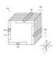
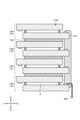
図1は、第1実施形態に係る調光装置を模式的に示す斜視図である。図2は、図1の調光装置の断面図である。図3は、複数のセルを設けたウエハを示す模式図である。図4は、図3のセルを複数積層させた断面図である。[First embodiment]
Fig. 1 is a perspective view showing a light control device according to a first embodiment. Fig. 2 is a cross-sectional view of the light control device shown in Fig. 1. Fig. 3 is a schematic view showing a wafer provided with a plurality of cells. Fig. 4 is a cross-sectional view of a plurality of stacked cells shown in Fig. 3.
なお、図に示すXYZ座標において、X方向は、前後方向であり、X1側はX2側の反対である。X1側は前側とも称し、X2側は後側とも称する。Y方向は、左右方向であり、Y1側はY2側の反対である。Y1側は左側とも称し、Y2側は右側とも称する。Z方向は、上下方向(積層方向)である。Z1側はZ2側の反対である。Z1側は上側とも称し、Z2側は下側とも称する。なお、Z方向は第1方向とも称せられ、X方向およびY方向は第2方向とも称せられる。例えば、第1方向の一方側は、Z方向のZ1側であり、第1方向の他方側は、Z方向のZ2側である。In the XYZ coordinate system shown in the figure, the X direction is the front-to-back direction, and the X1 side is opposite the X2 side. The X1 side is also called the front side, and the X2 side is also called the rear side. The Y direction is the left-to-right direction, and the Y1 side is opposite the Y2 side. The Y1 side is also called the left side, and the Y2 side is also called the right side. The Z direction is the up-down direction (stacking direction). The Z1 side is opposite the Z2 side. The Z1 side is also called the upper side, and the Z2 side is also called the lower side. The Z direction is also called the first direction, and the X and Y directions are also called the second directions. For example, one side of the first direction is the Z1 side of the Z direction, and the other side of the first direction is the Z2 side of the Z direction.
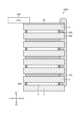
図1および図2に示すように、第1実施形態に係る調光装置100は、パネルユニット110と、導電部材500と、外部接続用配線の一例であるフレキシブルプリント基板(FPC:FLEXIBLE PRINTED CIRCUITS)400と、を備える。外部接続用配線400は、フレキシブルプリント基板に限らず導線であっても良い。1 and 2, the
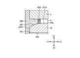
図2に示すように、本実施形態では、パネルユニット110は、Z方向(第1方向)に複数(実施形態では4つ)の調光パネル1を積層させて形成される。調光パネル1は、本実施形態では、正方形であるが、本発明はこれに限定されず、5角形などの多角形も含む。2, in this embodiment, the
具体的には、図2に示すように、4つの調光パネル1は、上側から順に、調光パネル1A、1B、1C、1Dが積層される。それぞれの調光パネル1は、下側に配置されるアレイ基板2と、上側に配置される対向基板3と、アレイ基板2および対向基板3の間に設けられるシール600と、シール600の内側に充填される液晶層4と、端子200と、を備える。なお、シール600の内側は、有効領域である。また、Z方向から見た場合に、アレイ基板2および対向基板3の大きさは同一である。そして、例えば、最も下側に位置する調光パネル1Dにおけるアレイ基板2の端子200に外部接続用配線(フレキシブルプリント基板)400が電気的に接続される。Specifically, as shown in FIG. 2, the four
また、パネルユニット110の側部には、導電部材500が上下方向に沿って延びている(後述の図10を参照)。導電部材500の材質は、例えば、銀(Ag)またはカーボン(C)などが適用可能である。導電部材500は、例えば、導電材を含むペーストをアレイ基板2等に塗布し硬化させて形成する。In addition, a
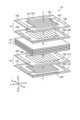
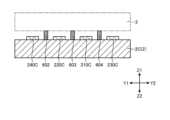
次に、積層させたウエハを上下に切り出して個片化してパネルユニット110を作製する手順を簡単に説明する。Next, we will briefly explain the procedure for cutting the stacked wafers into individual pieces at the top and bottom to create the
図3に示すように、ウエハ45には、シール600および液晶層4が一定間隔で配置される。破線は分割線47を示す。このように、ウエハ45上で液晶セルを複数作製する。次いで、図4に示すように、この液晶セルを有するウエハ45を、透光性接着剤720(例えばOCR)を用いて接着しつつ上下に積層する。そして、図4に示す分割線47に沿ってワイヤーソーやダイシングなどで切断して個片化する。これにより、パネルユニット110が完成する。As shown in FIG. 3, the
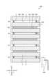
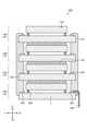
次いで、パネルユニット110を構成するアレイ基板2および対向基板3の配線および端子について詳細に説明する。図5は、図2に示す上側から1番目と2番目の調光パネルにおけるアレイ基板の平面図である。図6は、図2に示す上側から1番目と2番目の調光パネルにおける対向基板の平面図である。図7は、図2に示す上側から3番目と4番目の調光パネルにおけるアレイ基板の平面図である。図8は、図2に示す上側から1番目と2番目の調光パネルにおける対向基板の平面図である。図9は、4枚の調光パネルを上下に離隔して配置した状態を示す分解斜視図である。図10は、図9に示す4枚の調光パネルを積層させた第1実施形態に係る調光装置を模式的に示す斜視図である。図11は、4つの導電部材と、それぞれの調光パネルにおいてアレイ基板および対向基板の電極と接続する導電部材との関係を示す表である。Next, the wiring and terminals of the
前述したように、図9を参照すると、4つの調光パネルは、上側から順に、調光パネル1A、調光パネル1B、調光パネル1Cおよび調光パネル1Dが積層される。As mentioned above, referring to Figure 9, the four dimming panels are stacked from the top as dimming
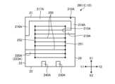
図5に示すように、調光パネル1Aおよび調光パネル1Bのアレイ基板2は、第1端子210、220、230、240と、液晶駆動電極250と、を備える。なお、アレイ基板2は、平面視で正方形であり、第1辺21、第2辺22、第3辺23および第4辺24を有する。第1辺21は、X1側に位置する。第2辺22は、X2側に位置する。第3辺23は、Y1側に位置する。第4辺24は、Y2側に位置する。As shown in Figure 5, the
第1端子210は、直線部213、215を有する。直線部213、215は、幅広の帯状体である。直線部213は、端211から端212まで延びる。直線部213は、第1辺21に沿って延びる。直線部215は、端212から端214まで延びる。端214は、配線251に接続される。アレイ基板2の中央には、液晶駆動電極250が設けられ、配線251は、液晶駆動電極250に電気的に接続される。配線251は、Y方向に延びる。液晶駆動電極250は、複数設けられ、それぞれがX方向に延びる。The
第1端子220は、直線部223、225を有する。直線部223、225は、幅広の帯状体である。直線部223は、端221から端222まで延びる。直線部223は、第2辺22に沿って延びる。直線部225は、端222から端224まで延びる。端224は、配線252に接続される。配線252は、液晶駆動電極250に接続される。配線252は、Y方向に延びる。The
第1端子230は、直線部233を有する。直線部233は、幅広の帯状体である。直線部233は、端231から端232まで延びる。直線部233は、第3辺23に沿って延びる。The
第1端子240は、直線部243を有する。直線部243は、幅広の帯状体である。直線部243は、端241から端242まで延びる。直線部243は、第4辺24に沿って延びる。The
図6に示すように、調光パネル1Aおよび調光パネル1Bの対向基板3は、第2端子310、320、330、340と、液晶駆動電極350と、を備える。なお、対向基板3は、平面視で正方形であり、第1辺31、第2辺32、第3辺33および第4辺34を有する。第1辺31は、X1側に位置する。第2辺32は、X2側に位置する。第3辺33は、Y1側に位置する。第4辺34は、Y2側に位置する。As shown in Figure 6, the opposing
第2端子310は、直線部313を有する。直線部313は、幅広の帯状体である。直線部313は、端311から端312まで延びる。直線部313は、第1辺31に沿って延びる。The
第2端子320は、直線部323を有する。直線部323は、幅広の帯状体である。直線部323は、端321から端322まで延びる。直線部323は、第2辺32に沿って延びる。The
第2端子330は、直線部333、335を有する。直線部333、335は、幅広の帯状体である。直線部333は、端331から端332まで延びる。直線部333は、第3辺33に沿って延びる。直線部335は、端332から端334まで延びる。端334は、配線351に接続される。対向基板3の中央には、液晶駆動電極350が設けられ、配線351は、液晶駆動電極350に電気的に接続される。配線351は、X方向に延びる。液晶駆動電極350は、複数設けられ、それぞれがY方向に延びる。The
第2端子340は、直線部343、345を有する。直線部343、345は、幅広の帯状体である。直線部343は、端341から端342まで延びる。直線部343は、第4辺34に沿って延びる。直線部345は、端342から端344まで延びる。端344は、配線352に接続される。配線352は、液晶駆動電極350に電気的に接続される。配線352は、X方向に延びる。The
次に、調光パネル1C、1Dについて説明するが、調光パネル1C、1Dは、調光パネル1A、1Bを時計回り方向(右回り方向)に90度回転させたものである。従って、調光パネル1C、1Dに含まれるアレイ基板2および対向基板3の配線、端子、および電極の位置も、調光パネル1A、1Bに含まれるアレイ基板2および対向基板3の配線、端子、および電極を時計回り方向(右回り方向)に90度回転させたものである。Next, the dimming
そして、図9に示すように、調光パネル1A、1B、1C、1Dを上下に積層してパネルユニット110を作製する。次に、図10に示すように、パネルユニット110の側部に導電部材500を設ける。具体的には、パネルユニット110のそれぞれの辺の側部に、4つの導電部材510、520、530、540を設ける。具体的には、例えば、銀やカーボンなどの導電材を含むペーストをパネルユニット110の側部に塗布したのち硬化させることにより導電部材500を形成する。ペーストは、調光パネル1におけるアレイ基板2の端子200および対向基板3の端子200に電気的に接続するように塗布する。従って、1つの調光パネル1におけるアレイ基板2の端子200と対向基板3の端子200とは、導電部材500を介して電気的に接続される。以上より、1つの導電部材500は、調光パネル1Dにおけるアレイ基板2の端子200および対向基板3の端子200と、調光パネル1Cにおけるアレイ基板2の端子200および対向基板3の端子200と、調光パネル1Bにおけるアレイ基板2の端子200および対向基板3の端子200と、調光パネル1Aにおけるアレイ基板2の端子200および対向基板3の端子200と、を電気的に接続する。Then, as shown in FIG. 9, the dimming
ここで、図11の表を説明する。例えば、調光パネル1Aにおけるアレイ基板の欄に記載された210(510)は、図5に示す第1端子210が導電部材510に接続されることを意味する。図5に示すように第1端子210は、X1側に位置する。図10に示すように、導電部材510もX1側に位置する。従って、ともにX1側に配置される導電部材510と第1端子210とが電気的に接続される。Here, the table in Figure 11 will be explained. For example, 210 (510) written in the column for the array substrate in the
また、調光パネル1Dにおける対向基板の欄に記載された340(520)は、図8に示す第2端子340が導電部材520に接続されることを意味する。図8に示すように第2端子340は、X2側に位置する。図10に示すように、導電部材520もX2側に位置する。従って、ともにX2側に配置される導電部材520と第2端子340とが電気的に接続される。なお、本実施形態に係る調光装置100においては、p波偏光用の液晶セルとs波偏光用の液晶セルとを積層して組み合わせている。Furthermore, 340 (520) written in the column for the opposing substrate in the
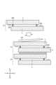
次いで、第1比較例を説明する。図12は、第1比較例に係るパネルユニットの調光パネルを積層する状態を示す模式図である。図13は、第1比較例に係るパネルユニットに1つの導電部材を設けた状態を示す模式図である。図14は、第1比較例に係る調光装置を示す模式図である。Next, a first comparative example will be described. Fig. 12 is a schematic diagram showing the state in which the dimming panels of the panel unit according to the first comparative example are stacked. Fig. 13 is a schematic diagram showing the state in which one conductive member is provided on the panel unit according to the first comparative example. Fig. 14 is a schematic diagram showing the dimming device according to the first comparative example.
図12から図14に示すように、第1比較例に係る調光装置100Aおよびパネルユニット110Aにおいては、アレイ基板2に対して対向基板3がY方向にずれて配置される。具体的には、対向基板3はアレイ基板2に対してY1側に位置がずれている。また、アレイ基板2の端子200の上側には対向基板3が対向配置されない。対向基板3の端子300の下側にはアレイ基板2が対向配置されない。以下、簡単に、第1比較例に係る調光装置100Aの作製手順を説明する。As shown in Figures 12 to 14, in the
まず、図12に示すように、アレイ基板2、対向基板3、シール600および液晶層4を含む調光パネル10を上下に積層する。上側の調光パネル10と下側の調光パネル10とを接合する際には、OCAなどの光学粘着シートである透光性接着剤720を用いる。これにより、図13に示すように、パネルユニット110Aが作製される。なお、図13に示すように、パネルユニット110Aにおいては、上側から順に、調光パネル10A、10B、10Cおよび10Dがこの順に積層される。First, as shown in Fig. 12, the
次に、図13に示すように、パネルユニット110Aの側部の一方側(Y2側)には、導電部材510を設ける。導電部材510は、それぞれの調光パネル10におけるアレイ基板2の端子200を上下に繋ぐ。また、図14に示すように、パネルユニット110Aの側部の他方側(Y1側)には、導電部材520を設ける。導電部材520は、それぞれの調光パネル10における対向基板3の端子300を上下に繋ぐ。なお、外部接続用配線400は、例えば、一番下に位置する調光パネル10におけるアレイ基板2の端子200に接続される。Next, as shown in FIG. 13, a
次いで、第2比較例を説明する。図15は、第2比較例に係る調光装置を示す模式図である。Next, we will explain the second comparative example. Figure 15 is a schematic diagram showing a dimming device related to the second comparative example.
図15に示すように、第2比較例に係る調光装置100Fおよびパネルユニット110Fにおいて、導電部材510、520はアレイ基板2の端子200に接続され且つ対向基板3には接続されない。また、アレイ基板2の端子200は導電部材510によって上下に繋がれて、調光パネル10Dの端子200にて外部接続用配線400に接続される。以下、簡単に、第2比較例に係る調光装置100Fを説明する。15, in the
図15に示すように、調光パネル10を上下に積層してパネルユニット110Fが形成される。調光パネル10は、アレイ基板2、対向基板3、シール600および液晶層4を含む。アレイ基板2は、対向基板3よりも大きい。具体的には、アレイ基板2は対向基板3よりもX方向及びY方向に大きく形成されており、アレイ基板2の各辺に設けられる端子200は、Z1側から見て対向基板3から露出されている。対向基板3には、端子が設けられない。パネルユニット110Fにおいては、上側から順に、調光パネル10A、10B、10Cおよび10Dがこの順に積層される。As shown in FIG. 15, a
パネルユニット110Fの側部の一方側(Y2側)には、導電部材510が設けられる。導電部材510は、それぞれの調光パネル10におけるアレイ基板2の端子200を上下に繋ぐ。また、パネルユニット110Fの側部の他方側(Y1側)には、導電部材520が設けられる。導電部材520は、それぞれの調光パネル10におけるアレイ基板2の端子200を上下に繋ぐ。なお、外部接続用配線(フレキシブルプリント基板)400は、例えば、一番下に位置する調光パネル10Dにおけるアレイ基板2の端子200に接続される。A
以上説明したように、第1実施形態の調光装置100は、第1端子210、220、230、240を有するアレイ基板2(第1基板)と第2端子310、330、330、340を有する対向基板3とを有する調光パネル1A、1B、1C、1が、上下方向(第1方向、Z方向)に複数積層されるパネルユニット110と、第1端子または第2端子に接続される外部接続用配線(フレキシブルプリント基板)400と、パネルユニット110における側部(第2方向の端部)に設けられ且つ上下方向に延びる導電部材500と、を備える。導電部材500は、パネルユニット110における最も上側(第1方向の一方側)に位置する調光パネル1Aから最も下側(第1方向の他方側)に位置する調光パネル1Dまで延び、且つ、それぞれの調光パネルにおける、アレイ基板2の第1端子と対向基板3の第2端子とを接続する。As described above, the dimming
前述したように、特許文献1では、1つの調光パネルにおけるアレイ基板の端子と対向基板の端子とのそれぞれに外部接続用配線400を1つずつ接続するため、調光装置全体に用いる外部接続用配線400の数が多くなる。具体的には特許文献1では、外部接続用配線400が8枚必要となる。As mentioned above, in
しかし、本実施形態及び第1、第2比較例では、図11の表で説明したように、例えば、調光パネル1Dのアレイ基板2の第1端子210、220と、調光パネル1Dの対向基板3の第2端子330、340との合計4か所に例えばフレキシブルプリント基板などの外部接続用配線400を接続すればよい。However, in this embodiment and the first and second comparative examples, as explained in the table of Figure 11, it is sufficient to connect
即ち、4つの調光パネルを積層した調光装置の場合、特許文献1では、外部接続用配線400が8枚必要となるが、本実施形態及び第1、第2比較例では、外部接続用配線400の数が4枚で済むことになり、外部接続用配線400の数を抑制できる。なお、4つの外部接続用配線400は、矩形状の調光装置100の各辺に1つずつ配置することができるため、4つの外部接続用配線400を1つの辺に集中させる場合よりも、外部接続用配線400の接続作業が容易になる。That is, in the case of a light control device having four stacked light control panels, eight
調光パネル1、1A、1B、1C、1Dは、上下方向から見て多角形の形状を有し、第1端子210、220、230、240および第2端子310、320、330、340は、多角形の辺に沿って延びる帯状体である。これによれば、調光パネル1、1A、1B、1C、1Dの縁に沿って幅広の端子が配置されるので、端子とフレキシブルプリント基板などの外部接続用配線400との接続作業が容易である。The dimming
また、第1比較例及び第2比較例においては、Z1側から見て、アレイ基板2の端子200が対向基板3から露出されているため、外部接続用配線(フレキシブルプリント基板)400と端子200との接続が第1実施形態に比べより容易となる。しかし、第1比較例及び第2比較例に係る導電部材510及び520においては、導電部材510及び520と基板との接続部分のZ方向距離が第1実施形態よりも大きい。例えば、第1比較例では、図13に示すように導電部材510は、調光パネル10Aのアレイ基板2、調光パネル10Bのアレイ基板2、調光パネル10Cおよび調光パネル10Dのアレイ基板2に接続されるが、対向基板3には接続されない。即ち、導電部材510と基板との接続部分同士のZ方向の距離は、1枚の調光パネル10の厚さになる。従って、第1比較例及び第2比較例においては、導電部材510及び520の導電性のペーストを塗布する際の制御が難しい。In addition, in the first and second comparative examples, the
これに対して、第1実施形態では、端子200が位置するアレイ基板2と対向基板3とが向かい合っており、導電部材510及び520は、全ての調光パネル10のアレイ基板2および対向基板3に接続される。即ち、導電部材510及び520と基板との接続部分同士のZ方向の距離は、アレイ基板2と対向基板3とのZ方向距離になる。従って、第1実施形態では、導電性ペーストの塗布面であるパネルユニット110の側面が第1比較例及び第2比較例に比べ平坦化されることで、導電部材510及び520の導電性のペーストを塗布する際の制御が容易となる。In contrast, in the first embodiment, the
さらに、第1比較例及び第2比較例においては、アレイ基板2と対向基板3の大きさが異なることや、一方の基板が他方の基板とZ方向で重ならない領域を有するため、上述の図3及び図4にて述べたようにアレイ基板2と対向基板3が複数形成されたウエハを複数積層させた状態でのダイシングが行えず、調光装置の製造効率の低下及び製造コストの増加となり得る。Furthermore, in the first and second comparative examples, since the
これに対して、第1実施形態においては、導電部材510及び520の導電性のペーストの塗布のしやすさ、積層されたウエハ上でアレイ基板2及び対向基板3を一括してダイシング可能とすることで製造効率の向上を図ることができる点で、第1比較例及び第2比較例にはないメリットを有している。また、第1実施形態では、アレイ基板2と対向基板3がY方向およびX方向でずれないで、Z方向で重なり合うため、パネルユニット110の額縁が狭くなり、調光装置100の小型化や狭額縁化にも貢献する。In contrast, the first embodiment has advantages not found in the first and second comparative examples in that the conductive paste of the
[第2実施形態]
次に、第2実施形態について説明する。図16は、第2実施形態に係る調光装置を模式的に示す斜視図である。図17は、図16に示す上側から1番目と2番目の調光パネルにおけるアレイ基板の平面図である。図18は、図16に示す上側から1番目と2番目の調光パネルにおける対向基板の平面図である。図19は、図16に示す上側から3番目と4番目の調光パネルにおけるアレイ基板の平面図である。図20は、図16に示す上側から3番目と4番目の調光パネルにおける対向基板の平面図である。[Second embodiment]
Next, the second embodiment will be described. Fig. 16 is a perspective view showing a light control device according to the second embodiment. Fig. 17 is a plan view of an array substrate in the first and second light control panels from the top shown in Fig. 16. Fig. 18 is a plan view of an opposing substrate in the first and second light control panels from the top shown in Fig. 16. Fig. 19 is a plan view of an array substrate in the third and fourth light control panels from the top shown in Fig. 16. Fig. 20 is a plan view of an opposing substrate in the third and fourth light control panels from the top shown in Fig. 16.
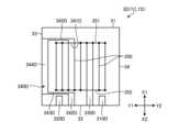
まず、パネルユニット110を構成するアレイ基板および対向基板の配線および端子について詳細に説明する。図17に示すように、調光パネル1Aおよび調光パネル1Bのアレイ基板2Aは、第1端子210A、220A、230A、240Aと、液晶駆動電極250と、を備える。第1辺21は、X1側に位置する。第2辺22は、X2側に位置する。第3辺23は、Y1側に位置する。第4辺24は、Y2側に位置する。First, the wiring and terminals of the array substrate and counter substrate that constitute the
第1端子210Aは、直線部216A、217A、218A、219A、を有する。直線部216Aは、端211Aから端212Aまで延びる。直線部217Aは、端212Aから端213Aまで延びる。直線部218Aは、端213Aから端214Aまで延びる。直線部219Aは、端214Aから端215Aまで延びる。端215Aは、配線251に接続される。直線部216Aは、第2辺22に沿って延びる。直線部217Aは、第4辺24に沿って延びる。直線部218Aは、第1辺21に沿って延びる。The
第1端子220Aは、直線部223Aを有する。直線部223Aは、端221AからX方向に沿って端222Aまで延びる。端222Aは、配線252に接続される。The
第1端子230Aは、端231Aから端232Aまで延びる。第1端子240Aは、端241Aから端242Aまで延びる。第1端子230Aは、第1端子240AよりもX2側に配置される。第1端子230Aおよび第1端子240Aは、第3辺23に設けられる。図18に示すように、調光パネル1Aおよび調光パネル1Bの対向基板3Aは、第2端子310A、320A、330A、340Aと、液晶駆動電極350と、を備える。The
第2端子310Aは、端311Aから端312Aまで延びる。第2端子320Aは、端321Aから端322Aまで延びる。第2端子310Aは、第2端子320AよりもY2側に配置される。第2端子310Aおよび第2端子320Aは、第2辺32に設けられる。The
第2端子330Aは、第3辺33に設けられる。第2端子340Aは、直線部346A、347A、348A、349Aを有する。直線部346Aは、端341Aから端342Aまで延びる。直線部346Aは、第3辺33に沿って延びる。直線部347Aは、端342Aから端343Aまで延びる。直線部347Aは、第1辺31に沿って延びる。直線部348Aは、端343Aから端344Aまで延びる。直線部347Aは、第4辺34に沿って延びる。直線部349Aは、端344Aから端345Aまで延びる。端345Aは、配線352に接続される。The
次に、調光パネル1C、1Dについて説明する。調光パネル1C、1Dにおけるアレイ基板の端子、配線および液晶駆動電極は、上側から見た状態で、調光パネル1Aおよび調光パネル1Bにおける対向基板の端子、配線および液晶駆動電極の位置と一致する。即ち、図19に示すアレイ基板と図18に示す対向基板について、端子、配線および液晶駆動電極の位置が同じである。また、図20に示す対向基板と図17に示すアレイ基板について、端子、配線および液晶駆動電極の位置が同じである。以下、具体的に説明する。Next, the dimming
図19に示すように、調光パネル1Cおよび調光パネル1Dのアレイ基板2Bは、第1端子210A、220A、230A、240Aと、液晶駆動電極250と、を備える。第1辺21は、X1側に位置する。第2辺22は、X2側に位置する。第3辺23は、Y1側に位置する。第4辺24は、Y2側に位置する。As shown in Figure 19, the
第1端子210Aは、直線部216A、217A、218A、219A、を有する。直線部216Aは、第3辺23に沿って延びる。直線部217Aは、第1辺21に沿って延びる。直線部218Aは、第4辺24に沿って延びる。第1端子210Aは、配線251に接続される。The
第1端子220Aは、直線部223Aを有する。直線部223Aは、第3辺23に設けられる。直線部223Aは、配線252に接続される。The
第1端子230Aおよび第1端子240Aは、第2辺22に設けられる。第1端子230Aは、第1端子240AよりもY2側に配置される。The
図20に示すように、調光パネル1Cおよび調光パネル1Dの対向基板3Bは、第2端子310A、320A、330A、340Aと、液晶駆動電極350と、を備える。As shown in FIG. 20, the opposing
第2端子310A、320Aは、第3辺33に設けられる。第2端子310Aは、第2端子320AよりもX1側に位置する。The
第2端子330Aは、第2辺32に設けられる。The
第2端子340Aは、直線部346A、347A、348A、349Aを有する。直線部346Aは、第2辺32に沿って延びる。直線部347Aは、第4辺34に沿って延びる。直線部348Aは、第1辺31に沿って延びる。直線部349Aの端345Aは、配線352に接続される。The
以上説明したように、第2実施形態によっても、4つの調光パネルを積層した調光装置の場合、特許文献1では、外部接続用配線400が8枚必要となるが、本実施形態では、外部接続用配線400の数が4枚で済むことになり、第1実施形態と同様に、外部接続用配線400の数を抑制できる。As described above, even in the second embodiment, in the case of a dimming device having four stacked dimming panels, eight
また、第1端子210Aの直線部217Aおよび第2端子340Aの直線部347Aは、辺の全域に亘って延びているため、外部接続用配線400を接続する範囲が長くなる。In addition, the
[第3実施形態]
次に、第3実施形態について説明する。図21は、第3実施形態に係る調光装置を模式的に示す斜視図である。図22は、図21に示す上側から1番目と2番目の調光パネルにおけるアレイ基板の平面図である。図23は、図21に示す上側から1番目と2番目の調光パネルにおける対向基板の平面図である。図24は、図21に示す上側から3番目と4番目の調光パネルにおけるアレイ基板の平面図である。図25は、図21に示す上側から3番目と4番目の調光パネルにおける対向基板の平面図である。[Third embodiment]
Next, a third embodiment will be described. Fig. 21 is a perspective view showing a light control device according to the third embodiment. Fig. 22 is a plan view of an array substrate in the first and second light control panels from the top shown in Fig. 21. Fig. 23 is a plan view of an opposing substrate in the first and second light control panels from the top shown in Fig. 21. Fig. 24 is a plan view of an array substrate in the third and fourth light control panels from the top shown in Fig. 21. Fig. 25 is a plan view of an opposing substrate in the third and fourth light control panels from the top shown in Fig. 21.
まず、第3実施形態に係る調光装置100Cにおけるパネルユニット110を構成するアレイ基板および対向基板の配線および端子について詳細に説明する。第3実施形態においては、全ての調光パネルにおいて、4つの端子が同一の第2辺に配置される。以下、具体的に説明する。First, the wiring and terminals of the array substrate and the opposing substrate constituting the
図22に示すように、調光パネル1Aおよび調光パネル1Bのアレイ基板2Cは、第1端子210C、220C、230C、240Cと、液晶駆動電極250と、を備える。第1辺21は、X1側に位置する。第2辺22は、X2側に位置する。第3辺23は、Y1側に位置する。第4辺24は、Y2側に位置する。As shown in Figure 22, the
第1端子210Cは、第2辺32に設けられる。第1端子210Cの端211Cは配線252に接続される。第1端子220Cは、直線部222C、223C、224C、225Cを有する。直線部222Cは、第2辺22から端226Cまで延びる。直線部223Cは、端226Cから端227Cまでに延びる。直線部224Cは、端227Cから端228Cまでに延びる。直線部225Cは、端228Cから端229Cまでに延びる。端229Cは、配線251に接続される。The
第1端子230Cは、第2辺22に設けられる。第1端子230Cは、第1端子210CよりもY2側に位置する。The
第1端子240Cは、第2辺22に設けられる。第1端子240Cは、直線部222CよりもY1側に位置する。The
アレイ基板2Cの第2辺22において、Y2側からY1側に向けて、第1端子230C、第1端子210C、第1端子220Cの直線部222Cおよび第1端子240Cが順に並んで配置される。On the
図23に示すように、調光パネル1Aおよび調光パネル1Bの対向基板3Cは、第2端子310C、320C、330C、340Cと、液晶駆動電極350と、を備える。As shown in FIG. 23, the opposing
第2端子310Cおよび第2端子320Cは、第2辺32に設けられる。第2端子310Cは、第2端子320CよりもY2側に配置される。The
第2端子330Cは、直線部332C、333C、334Cを有する。直線部332Cは、第2辺32に沿って延びる。直線部333Cは、第4辺34に沿って延びる。直線部334Cは、端331Cを有し、端331Cは、配線352に接続される。The
第2端子340Cは、直線部342C、343C、344Cを有する。直線部342Cは、第2辺32に沿って延びる。直線部343Cは、第3辺33に沿って延びる。直線部344Cは、端341Cを有し、端341Cは、配線351に接続される。The
次に、調光パネル1C、1Dについて説明する。調光パネル1C、1Dにおけるアレイ基板の端子、配線および液晶駆動電極は、上側から見た状態で、調光パネル1Aおよび調光パネル1Bにおける対向基板の端子、配線および液晶駆動電極の位置と一致する。即ち、図24に示すアレイ基板と図23に示す対向基板について、端子、配線および液晶駆動電極の位置が同じである。また、図25に示す対向基板と図22に示すアレイ基板について、端子、配線および液晶駆動電極の位置が同じである。以下、具体的に説明する。Next, the dimming
図24に示すように、調光パネル1Cおよび調光パネル1Dのアレイ基板2Dは、第1端子210D、220D、230D、240Dと、液晶駆動電極250と、を備える。第1辺21は、X1側に位置する。第2辺22は、X2側に位置する。第3辺23は、Y1側に位置する。第4辺24は、Y2側に位置する。As shown in Figure 24, the
第1端子210Dは、直線部212D、213D、214Dを有する。直線部212Dは、第2辺22に沿って延びる。直線部213Dは、第4辺24に沿って延びる。直線部214Dは、端211Dを有し、端211Dは、配線251に接続される。The
第1端子220Dは、直線部222D、223D、224Dを有する。直線部222Dは、第2辺22に沿って延びる。直線部223Dは、第3辺23に沿って延びる。直線部224Dは、端221Dを有し、端221Dは、配線252に接続される。The
第1端子230D、240Dは、第2辺22に設けられる。第1端子230Dは、第1端子240DよりもY2側に位置する。The
図25に示すように、調光パネル1Cおよび調光パネル1Dの対向基板3Dは、第2端子310D、320D、330D、340Dと、液晶駆動電極350と、を備える。As shown in FIG. 25, the opposing
第2端子310Dおよび第2端子320Dは、第2辺32に設けられる。第2端子310Dは、第2端子320DよりもY2側に位置する。The
第2端子330Dは、第2辺32に設けられる。第2端子330Dは、配線352に接続される。The
第2端子340Dは、直線部342D、343D、344D、345Dを有する。直線部342Dは、第2辺32に設けられる。直線部343Dは、直線部342Dの先端からY1側に延びる。直線部344Dは、第3辺33に沿って延びる。直線部345Dは、Y方向に延び、端341Dが配線351に接続される。The
以上説明したように、第3実施形態によっても、第1および第2実施形態と同様に、例えばフレキシブルプリント基板のような外部接続用配線400の数を抑制できる。特に、第3実施形態では、一つの辺に全ての端子が配置されるため、4つの外部接続用配線400が同一方向に引き出され、外部接続用配線400に接続される外部コネクタを1つにすることができる。As described above, the third embodiment can also reduce the number of
[第1変形例]
次に、第1変形例を説明する。図26は、第1変形例に係る調光装置を示す模式的な断面図である。[First Modification]
Next, a first modified example will be described below. Fig. 26 is a schematic cross-sectional view showing a light control device according to the first modified example.
図26に示すように、第1変形例においては、アレイ基板2Eの端部に面取部25Eを設けている。面取部25Eは、表面20aと側面20cとの角部に設けられる。面取部25Eは、例えば、断面において傾斜面で示される。傾斜面は、導電部材500に近づくに従って下側に傾斜する。つまり、面取部25Eは、アレイ基板2Eと対向基板3との上下距離がY1側に向かうに従って大きくなる形状に形成される。面取部25Eは、例えば、アレイ基板2Eの表面(上面)20aの端251Eと、アレイ基板2Eの側面20cの端252Eとを結ぶ平面である。As shown in FIG. 26, in the first modified example, a chamfered portion 25E is provided at the end of the
以上説明したように、第1変形例では、Y1側に向かうに従って上下方向の距離(Z方向の距離)が大きくなる面取部25Eを有するため、例えば、導電性のペーストを塗布して導電部材500を形成する際に、面取部25Eからペーストが流入するので、導電部材500の成形作業が容易である。As described above, the first modified example has a chamfered portion 25E whose vertical distance (distance in the Z direction) increases toward the Y1 side. Therefore, for example, when applying conductive paste to form the
[第2変形例]
次に、第2変形例を説明する。図27は、第2変形例に係る調光装置を示す模式的な断面図である。[Second Modification]
Next, a second modified example will be described with reference to Fig. 27, which is a schematic cross-sectional view showing a light control device according to the second modified example.
図27に示すように、第2変形例においては、アレイ基板2Fの端部に曲面部25Fを設けている。曲面部25Fは、表面20aと側面20cとの角部に設けられる。曲面部25Fは、アレイ基板2Eと対向基板3との上下距離がY1側に向かうに従って大きくなる形状に形成される。曲面部25Fは、対向基板3に向けて凸状に湾曲する。As shown in Figure 27, in the second modified example, a
以上説明したように、第2変形例では、凸状に湾曲する曲面部25Fを有するため、例えば、導電性のペーストを塗布して導電部材500を形成する際に、曲面部25Fからペーストが流入するので、導電部材500の成形作業が容易である。As described above, the second modified example has a
[第3変形例]
次に、第3変形例を説明する。図28は、第3変形例に係る調光装置を示す模式的な断面図である。[Third Modification]
Next, a third modified example will be described below. Fig. 28 is a schematic cross-sectional view showing a light control device according to the third modified example.
図28に示すように、第3変形例においては、導電部材を2層構造にしている。つまり、実施形態で説明した導電部材500は、1層構造であるが、第3変形例に係る導電部材550は、第1層551の上に第2層552を形成した2層構造である。具体的には、第1層551として、粘度の低いペーストを塗布し、第1層551の上に、第2層552として粘度の高いペーストを塗布したのち、ペーストを硬化させて導電部材550を形成する。なお、粘度の低いペーストとしては、例えば、銀(Ag)のペーストが好ましく、粘度の高いペーストとしては、例えば、カーボン(C)のペーストが好ましい。As shown in FIG. 28, in the third modified example, the conductive member has a two-layer structure. That is, the
以上説明したように、第3変形例では、導電部材500は、銀を含む第1層551と、第1層551の上に積層され且つカーボンを含む第2層552とを有する。As described above, in the third modified example, the
導電部材500は、例えば導電材を含むペーストで塗布して乾燥させることにより形成する。ここで、低粘度のペーストの方が高粘度のペーストよりも収縮率が高い。仮に、第1層目に高粘度のペーストを塗布したのち、第2層目に高粘度のペーストを塗布して、ペースト全体を乾燥させると、第2層目にひびなどが入りやすい。従って、第1層目に粘度の低い銀のペーストを塗布したのち、第2層目に、銀よりも粘度の高いカーボンのペーストを塗布することにより、導電部材500を形成することが好ましい。The
[第4変形例]
次に、第4変形例を説明する。図29は、第4変形例に係る調光装置を示す模式的な断面図である。[Fourth Modification]
Next, a fourth modified example will be described below. Fig. 29 is a schematic cross-sectional view showing a light control device according to the fourth modified example.
図29に示すように、第4変形例においては、アレイ基板2Gの側面20cに凹凸部25Gを設けている。換言すると、凹凸部25Gは、溝でもある。つまり、アレイ基板2Gの側面20cに、上下方向に沿って、凸部と凹部とが交互に配置されている。As shown in Fig. 29, in the fourth modified example,
以上説明したように、第4変形例では、アレイ基板2Gの側面20cには、凹凸部25Gが設けられる。導電部材500を、例えば導電材を含むペーストで塗布して乾燥させることによって形成する場合、ペーストが凹凸部25Gの溝の中に入って硬化する。このため、導電部材500がアレイ基板2Gにより強固に固定される。As described above, in the fourth modified example, the
[第5変形例]
次に、第5変形例を説明する。図30は、第5変形例に係る調光装置において、アレイ基板と対向基板を導通体で接続した調光パネルを示す模式的な断面図である。図31は、図30の調光パネルを積層したパネルユニットを示す模式図である。図32は、図31のパネルユニットの側部に導電部材を設けた模式図である。[Fifth Modification]
Next, a fifth modified example will be described. Fig. 30 is a schematic cross-sectional view showing a light control panel in which an array substrate and an opposing substrate are connected by a conductor in a light control device according to the fifth modified example. Fig. 31 is a schematic diagram showing a panel unit in which the light control panels of Fig. 30 are stacked. Fig. 32 is a schematic diagram in which a conductive member is provided on the side of the panel unit of Fig. 31.
第5変形例では、アレイ基板2と対向基板3とを導通体43で上下に電気的に接続すると共に導通体43に導電部材560を電気的に接続している。以下、具体的に説明する。In the fifth modified example, the
まず、図30に示すように、アレイ基板2の表面20aに電極41を形成する。電極41は、例えばY方向の全体に延び、例えば液晶駆動電極250に接続される。また、対向基板3の表面3aおよび裏面3bの端部に電極40を形成する。その後、図31に示すように、電極40と電極41とを接続するように、上下方向に延びる導通体43を設ける。First, as shown in Fig. 30, an
そして、図32に示すように、パネルユニット110の側部に導電部材560を設ける。導電部材560は、側方(Y方向)に突出する突出部561が上下に間隔をおいて複数設けられる。突出部561の先端は、導通体43と電気的に接続される。32, a
以上説明したように、第5変形例では、アレイ基板2の第1端子210と対向基板3の第2端子310とを導通体43で接続し、導通体43に導電部材500を接続している。アレイ基板2の第1端子210と対向基板3の第2端子310とは、導通体43と導電部材500との双方で接続されるため、より導通性が高くなる。As described above, in the fifth modified example, the
[第6変形例]
次に、第6変形例を説明する。図33は、第6変形例に係る調光装置を示す模式的な断面図である。[Sixth Modification]
Next, a sixth modified example will be described with reference to Fig. 33, which is a schematic cross-sectional view showing a light control device according to the sixth modified example.
第6変形例においては、パネルユニット110において、導電部材500に接続するITO膜を設け、ITO膜に例えばフレキシブルプリント基板などの外部接続用配線400を接続している。以下、具体的に説明する。In the sixth variant, an ITO film is provided in the
図33に示すように、調光装置100Dにおいては、パネルユニット110の最も上側に配置した対向基板3の上面(裏面30b)の上にITO膜44を設ける。ITO膜44はY方向の略全体に亘って形成する。ITO膜44におけるY1側の端部に外部接続用配線400を接続している。ITO膜44は、透光性導電膜の一例である。As shown in FIG. 33, in the
以上説明したように、第6変形例では、対向基板3の上面には、導電部材500に接続されたITO膜44が形成される。ITO膜44は、外部接続用配線400と接続される。As described above, in the sixth modified example, an
前述した実施形態および変形例では、外部接続用配線400は、端子200に接続している。しかし、本変形例では、外部接続用配線400は、導電部材500およびITO膜44を介して端子200と接続されるため、対向基板3の上面のように端子がない部位にも外部接続用配線400を接続することができる。In the above-described embodiment and modified example, the
[第7変形例]
次に、第7変形例を説明する。図34は、第7変形例に係る調光装置を示す模式的な断面図である。[Seventh Modification]
Next, a seventh modification will be described with reference to Fig. 34, which is a schematic cross-sectional view showing a light control device according to the seventh modification.
第7変形例においては、パネルユニット110の最も上側に配置した対向基板3にITO膜44を形成し、当該ITO膜44に例えばフレキシブルプリント基板などの外部接続用配線400を接続した。これに対して、第7変形例においては、パネルユニット110の最も下側に配置したアレイ基板2にITO膜44を形成し、当該ITO膜44に外部接続用配線400を接続した。以下、具体的に説明する。In the seventh modified example, an
図34に示すように、調光装置100Eにおいては、パネルユニット110の最も下側に配置したアレイ基板2の下面(裏面20b)にITO膜44を設ける。ITO膜44はY方向の略全体に亘って形成する。ITO膜44におけるY1側の端部の下に外部接続用配線400を接続している。As shown in Figure 34, in the
以上説明したように、第7変形例では、アレイ基板2の下面2b(第1方向の他方側の面)には、導電部材500に接続されたITO膜44が形成され、ITO膜44は、外部接続用配線400と接続される。As described above, in the seventh modified example, an
前述した実施形態および変形例では、外部接続用配線400は、端子200に接続している。しかし、本変形例では、外部接続用配線400は、導電部材500およびITO膜44を介して端子200と接続されるため、アレイ基板2の下面2bのように端子がない部位にも外部接続用配線400を接続することができる。In the above-described embodiment and modified example, the
[第8変形例]
図35は、第8変形例に係る調光装置を示す模式的な断面図である。図36は、図35の調光装置を示す模式的な平面図である。[Eighth Modification]
Fig. 35 is a schematic cross-sectional view showing a light control device according to an eighth modified example. Fig. 36 is a schematic plan view showing the light control device of Fig. 35.
第6変形例においては、パネルユニット110の最も上側に配置した対向基板3にITO膜44を形成し、当該ITO膜44に例えばフレキシブルプリント基板などの外部接続用配線400を接続した。これに対して、第8変形例においては、パネルユニット110の最も上側に配置した対向基板3に金属配線46を設け、当該金属配線46に外部接続用配線400を接続した。以下、具体的に説明する。In the sixth modified example, an
図35に示すように、調光装置100Gにおいては、パネルユニット110の最も上側に配置した対向基板3の上面(裏面30b)に金属配線46を設ける。金属配線46は、不透明である。図36に示すように、シール600の内側は有効領域である。金属配線46は、シール600の外側を囲むように設けられる。4つの導電部材500のそれぞれは、外部接続用配線400に接続される。As shown in FIG. 35, in the
以上説明したように、第8変形例では、対向基板3の上面(裏面30b)に金属配線46が設けられ、金属配線46は、外部接続用配線400と接続されるため、対向基板3の上面のように端子がない部位にも外部接続用配線400を接続することができる。As described above, in the eighth modified example,
[第9変形例]
次に、第9変形例を説明する。図37は、第9変形例に係る調光装置におけるアレイ基板の平面図である。図38は、図37のXXXVIII-XXXVIII線による断面図である。[Ninth Modification]
Next, a ninth modification will be described. Fig. 37 is a plan view of an array substrate in a light control device according to the ninth modification. Fig. 38 is a cross-sectional view taken along line XXXVIII-XXXVIII in Fig. 37.
図37および図38に示すように、第9変形例では、アレイ基板2の複数の端子(第1端子210C、220C、230C、240C)について、Y方向に隣接する端子の間に、シール600の隔壁部602、603、604を設けている。シール600は、円環部601と、隔壁部602、603、604と、を有する。円環部601の内周側には、液晶層4が充填される。隔壁部602、603、604は、円環部601からX2側に向けて延びる。隔壁部602は、第1端子240Cおよび220Cとの間に位置する。隔壁部603は、第1端子220Cおよび210Cとの間に位置する。隔壁部604は、第1端子210Cおよび230Cの間に位置する。37 and 38, in the ninth modified example, for a plurality of terminals (
以上説明したように、第9変形例では、各端子210C、220C、230C、240Cの間に隔壁部602、603、604を設けているため、隣接する端子間のショートを抑制することができる。As described above, in the ninth variant,
1、1A、1B、1C、1D 調光パネル
2、2A、2B、2C、2D、2E、2F、2G アレイ基板(第1基板、下基板)
3、3A、3B、3C、3D 対向基板(第2基板、上基板)
4 液晶層
10、10A、10B、10C、10D 調光パネル
20a 表面
20b 裏面
20c 側面
21 第1辺
22 第2辺
23 第3辺
24 第4辺
25E 面取部
25F 曲面部
25G 凹凸部
31 第1辺
32 第2辺
33 第3辺
34 第4辺
40、41 電極
43 導通体
44 ITO膜(透光性導電膜)
46 金属配線
100、100A、100C、100D、100E、100F、100G 調光装置
110、110A、110F パネルユニット
200 端子
210、210A、210C、210D、220、220A、220C、220D、230、230A、230C、230D、240、240A、240C 第1端子
250 液晶駆動電極
300 端子
310、310A、310C、310D、320、320A、320C、320D、330、330A、330C、330D、340、340A、340C、340D 第2端子
350 液晶駆動電極
400 外部接続用配線(フレキシブルプリント基板)
500、510、520、530、540、550、560 導電部材
551 第1層
552 第2層
561 突出部
600 シール
601 円環部
602、603、604 隔壁部
720 透光性接着剤1, 1A, 1B, 1C, 1D:
3, 3A, 3B, 3C, 3D Opposite board (second board, upper board)
4
46
500, 510, 520, 530, 540, 550, 560
Claims (8)
Translated fromJapanese前記第1端子および前記第2端子の少なくともいずれかに接続される外部接続用配線と、
前記パネルユニットにおける前記第1方向に交差する第2方向の端部に設けられ且つ前記第1方向に延びる導電部材と、
を備え、
前記導電部材は、
前記パネルユニットにおける最も前記第1方向の一方側に位置する調光パネルから最も前記第1方向の他方側に位置する調光パネルまで延び、且つ、
それぞれの前記調光パネルにおける、前記第1基板の前記第1端子と前記第2基板の前記第2端子とを接続し、
それぞれの前記調光パネルにおいて、
前記第1基板の前記第1端子と前記第2基板の前記第2端子とは導通体で接続され、当該導通体に、前記導電部材が接続される、
調光装置。 A panel unit in which a plurality of light control panels each having a first substrate having a first terminal and a second substrate overlapping the first substrate and having a second terminal are stacked in a first direction;
an external connection wiring connected to at least one of the first terminal and the second terminal;
a conductive member provided at an end of the panel unit in a second direction intersecting the first direction and extending in the first direction;
Equipped with
The conductive member is
The panel unit extends from a light control panel located closest to one side in the first direction to a light control panel located closest to the other side in the first direction, and
The first terminal of the first substrate and the second terminal of the second substrate in each of the light control panelsare connected to each other;
In each of the light control panels,
the first terminal of the first substrate and the second terminal of the second substrate are connected by a conductor, and the conductive member is connected to the conductor;
Dimmer.
前記第1端子および前記第2端子は、前記多角形の辺に沿って延びる帯状体の直線部を含む、
請求項1に記載の調光装置。 The light control panel has a polygonal shape when viewed from the first direction,
The first terminal and the second terminal include straight portions of strips extending along sides of the polygon.
The light control device according to claim 1 .
前記第1基板の前記第2基板側の表面と前記第2基板の前記第1基板側の表面との少なくともいずれかにおける前記第2方向の一方側の端部は、
前記第1基板と前記第2基板との前記第1方向に沿った距離が、前記第2方向の一方側に向かうに従って大きくなる面取部を有する、
請求項1または2に記載の調光装置。 Regarding the first substrate and the second substrate included in one of the light control panels,
An end portion on one side in the second direction of at least one of a surface of the first substrate facing the second substrate and a surface of the second substrate facing the first substrate is
a chamfered portion in which the distance between the first substrate and the second substrate in the first direction increases toward one side in the second direction;
The light control device according to claim 1 or 2.
前記第1基板の前記第2基板側の表面と前記第2基板の前記第1基板側の表面との少なくともいずれかにおける前記第2方向の一方側の端部は、
前記第1基板と前記第2基板との前記第1方向に沿った距離が前記第2方向の一方側に向かうに従って大きくなり、且つ、凸状に湾曲する曲面部を有する、
請求項1または2に記載の調光装置。 Regarding the first substrate and the second substrate included in one of the light control panels,
An end portion on one side in the second direction of at least one of a surface of the first substrate facing the second substrate and a surface of the second substrate facing the first substrate is
a distance between the first substrate and the second substrate in the first direction increases toward one side in the second direction, and the first substrate has a curved surface portion that is convexly curved;
The light control device according to claim 1 or 2.
請求項1に記載の調光装置。 The conductive member has a first layer including silver and a second layer including carbon laminated on the first layer.
The light control device according to claim 1 .
請求項1に記載の調光装置。 a side surface provided at an end portion in the second direction of at least one of the first substrate and the second substrate has an uneven portion;
The light control device according to claim 1 .
前記第1基板に対して前記第1方向の一方側に前記第2基板が配置され、
前記第2基板の前記第1方向の一方側の面には、前記導電部材に接続された透光性導電膜が形成され、
当該透光性導電膜は、前記外部接続用配線と接続される、
請求項1に記載の調光装置。 Regarding the light control panel located closest to one side in the first direction provided in the panel unit,
the second substrate is disposed on one side of the first substrate in the first direction,
a transparent conductive film connected to the conductive member is formed on one surface of the second substrate in the first direction;
the transparent conductive film is connected to the external connection wiring;
The light control device according to claim 1 .
前記第1基板に対して前記第1方向の一方側に前記第2基板が配置され、
前記第1基板の前記第1方向の他方側の面には、前記導電部材に接続された透光性導電膜が形成され、
当該透光性導電膜は、前記外部接続用配線と接続される、
請求項1に記載の調光装置。 Regarding the light control panel located closest to the other side in the first direction in the panel unit,
the second substrate is disposed on one side of the first substrate in the first direction,
a transparent conductive film connected to the conductive member is formed on the other surface of the first substrate in the first direction;
the transparent conductive film is connected to the external connection wiring;
The light control device according to claim 1 .
Applications Claiming Priority (3)
| Application Number | Priority Date | Filing Date | Title |
|---|---|---|---|
| JP2022009932 | 2022-01-26 | ||
| JP2022009932 | 2022-01-26 | ||
| PCT/JP2022/043426WO2023145225A1 (en) | 2022-01-26 | 2022-11-24 | Light control device |
Publications (3)
| Publication Number | Publication Date |
|---|---|
| JPWO2023145225A1 JPWO2023145225A1 (en) | 2023-08-03 |
| JPWO2023145225A5 JPWO2023145225A5 (en) | 2024-08-28 |
| JP7672516B2true JP7672516B2 (en) | 2025-05-07 |
Family
ID=87471420
Family Applications (1)
| Application Number | Title | Priority Date | Filing Date |
|---|---|---|---|
| JP2023576651AActiveJP7672516B2 (en) | 2022-01-26 | 2022-11-24 | Light control device |
Country Status (4)
| Country | Link |
|---|---|
| US (1) | US20240361648A1 (en) |
| JP (1) | JP7672516B2 (en) |
| CN (1) | CN222813031U (en) |
| WO (1) | WO2023145225A1 (en) |
Citations (4)
| Publication number | Priority date | Publication date | Assignee | Title |
|---|---|---|---|---|
| US20050195488A1 (en) | 2002-09-20 | 2005-09-08 | Mccabe Ian A. | Electro-optic mirror cell |
| JP2009158755A (en) | 2007-12-27 | 2009-07-16 | Kyocera Corp | Substrate connection structure and electronic device |
| WO2017175796A1 (en) | 2016-04-05 | 2017-10-12 | 凸版印刷株式会社 | Light dimming module |
| JP2020027210A (en) | 2018-08-15 | 2020-02-20 | 大日本印刷株式会社 | Design material and method for manufacturing laminated polymer dispersion type liquid crystal device used for the same |
Family Cites Families (3)
| Publication number | Priority date | Publication date | Assignee | Title |
|---|---|---|---|---|
| JPH0452732Y2 (en)* | 1985-05-21 | 1992-12-11 | ||
| JPH10197906A (en)* | 1996-11-14 | 1998-07-31 | Nikon Corp | Electrochromic device |
| JPH11316395A (en)* | 1998-03-05 | 1999-11-16 | Nikon Corp | Electrochromic device |
- 2022
- 2022-11-24JPJP2023576651Apatent/JP7672516B2/enactiveActive
- 2022-11-24CNCN202290000863.7Upatent/CN222813031U/enactiveActive
- 2022-11-24WOPCT/JP2022/043426patent/WO2023145225A1/ennot_activeCeased
- 2024
- 2024-07-12USUS18/771,627patent/US20240361648A1/enactivePending
Patent Citations (4)
| Publication number | Priority date | Publication date | Assignee | Title |
|---|---|---|---|---|
| US20050195488A1 (en) | 2002-09-20 | 2005-09-08 | Mccabe Ian A. | Electro-optic mirror cell |
| JP2009158755A (en) | 2007-12-27 | 2009-07-16 | Kyocera Corp | Substrate connection structure and electronic device |
| WO2017175796A1 (en) | 2016-04-05 | 2017-10-12 | 凸版印刷株式会社 | Light dimming module |
| JP2020027210A (en) | 2018-08-15 | 2020-02-20 | 大日本印刷株式会社 | Design material and method for manufacturing laminated polymer dispersion type liquid crystal device used for the same |
Also Published As
| Publication number | Publication date |
|---|---|
| JPWO2023145225A1 (en) | 2023-08-03 |
| WO2023145225A1 (en) | 2023-08-03 |
| CN222813031U (en) | 2025-04-29 |
| US20240361648A1 (en) | 2024-10-31 |
Similar Documents
| Publication | Publication Date | Title |
|---|---|---|
| CN108957880B (en) | Array substrate, display panel and manufacturing method thereof | |
| KR20180095471A (en) | Method for manufacturing light emitting module and light emitting module | |
| CN114072758B (en) | Display device and method of manufacturing the same | |
| JP7012130B1 (en) | Micro LED display panel and its manufacturing method | |
| CN109840035B (en) | Display panel and display device | |
| CN113689788A (en) | Surface Display Module | |
| CN106206614A (en) | Flexible display panel and flexible display device | |
| WO2018051658A1 (en) | Solar cell module | |
| JP7672516B2 (en) | Light control device | |
| CN108598102B (en) | Light emitting device | |
| CN1662846A (en) | Comprising devices for connection to electronic control circuits and display units, especially liquid crystal units or photovoltaic units | |
| CN222564281U (en) | Display substrate and display panel | |
| JP7672502B2 (en) | Dimmers and panels | |
| CN116125709A (en) | Display module and display device | |
| CN108630114A (en) | A kind of LED display unit group and display panel | |
| CN112509992B (en) | Display panel, electronic device and method for manufacturing display panel | |
| CN111383545A (en) | Light board module for LED display | |
| CN115985895A (en) | Light emitting diode packaging structure, display panel and splicing type display device | |
| JP2023182313A (en) | Dimmer device | |
| JP2011155132A (en) | Solar cell module, and method of manufacturing the same | |
| CN219780849U (en) | Display panel | |
| JPS59138355A (en) | Multi-layer mounting structure of memory device | |
| JP2024055126A (en) | Light control device and method for manufacturing the same | |
| CN118742105B (en) | Display panel, method for manufacturing display panel, and electronic device | |
| CN114171656B (en) | Receiving substrate and manufacturing method thereof |
Legal Events
| Date | Code | Title | Description |
|---|---|---|---|
| A521 | Request for written amendment filed | Free format text:JAPANESE INTERMEDIATE CODE: A523 Effective date:20240614 | |
| A621 | Written request for application examination | Free format text:JAPANESE INTERMEDIATE CODE: A621 Effective date:20240614 | |
| A131 | Notification of reasons for refusal | Free format text:JAPANESE INTERMEDIATE CODE: A131 Effective date:20250121 | |
| A521 | Request for written amendment filed | Free format text:JAPANESE INTERMEDIATE CODE: A523 Effective date:20250317 | |
| TRDD | Decision of grant or rejection written | ||
| A01 | Written decision to grant a patent or to grant a registration (utility model) | Free format text:JAPANESE INTERMEDIATE CODE: A01 Effective date:20250401 | |
| A61 | First payment of annual fees (during grant procedure) | Free format text:JAPANESE INTERMEDIATE CODE: A61 Effective date:20250422 | |
| R150 | Certificate of patent or registration of utility model | Ref document number:7672516 Country of ref document:JP Free format text:JAPANESE INTERMEDIATE CODE: R150 |