JP7668944B2 - Light-emitting device - Google Patents
Light-emitting deviceDownload PDFInfo
- Publication number
- JP7668944B2 JP7668944B2JP2024155115AJP2024155115AJP7668944B2JP 7668944 B2JP7668944 B2JP 7668944B2JP 2024155115 AJP2024155115 AJP 2024155115AJP 2024155115 AJP2024155115 AJP 2024155115AJP 7668944 B2JP7668944 B2JP 7668944B2
- Authority
- JP
- Japan
- Prior art keywords
- effect transistor
- field effect
- light
- layer
- drain
- Prior art date
- Legal status (The legal status is an assumption and is not a legal conclusion. Google has not performed a legal analysis and makes no representation as to the accuracy of the status listed.)
- Active
Links
Images


Classifications
- H—ELECTRICITY
- H10—SEMICONDUCTOR DEVICES; ELECTRIC SOLID-STATE DEVICES NOT OTHERWISE PROVIDED FOR
- H10D—INORGANIC ELECTRIC SEMICONDUCTOR DEVICES
- H10D86/00—Integrated devices formed in or on insulating or conducting substrates, e.g. formed in silicon-on-insulator [SOI] substrates or on stainless steel or glass substrates
- H10D86/40—Integrated devices formed in or on insulating or conducting substrates, e.g. formed in silicon-on-insulator [SOI] substrates or on stainless steel or glass substrates characterised by multiple TFTs
- H10D86/421—Integrated devices formed in or on insulating or conducting substrates, e.g. formed in silicon-on-insulator [SOI] substrates or on stainless steel or glass substrates characterised by multiple TFTs having a particular composition, shape or crystalline structure of the active layer
- H10D86/423—Integrated devices formed in or on insulating or conducting substrates, e.g. formed in silicon-on-insulator [SOI] substrates or on stainless steel or glass substrates characterised by multiple TFTs having a particular composition, shape or crystalline structure of the active layer comprising semiconductor materials not belonging to the Group IV, e.g. InGaZnO
- G—PHYSICS
- G09—EDUCATION; CRYPTOGRAPHY; DISPLAY; ADVERTISING; SEALS
- G09G—ARRANGEMENTS OR CIRCUITS FOR CONTROL OF INDICATING DEVICES USING STATIC MEANS TO PRESENT VARIABLE INFORMATION
- G09G3/00—Control arrangements or circuits, of interest only in connection with visual indicators other than cathode-ray tubes
- G09G3/20—Control arrangements or circuits, of interest only in connection with visual indicators other than cathode-ray tubes for presentation of an assembly of a number of characters, e.g. a page, by composing the assembly by combination of individual elements arranged in a matrix no fixed position being assigned to or needed to be assigned to the individual characters or partial characters
- G09G3/22—Control arrangements or circuits, of interest only in connection with visual indicators other than cathode-ray tubes for presentation of an assembly of a number of characters, e.g. a page, by composing the assembly by combination of individual elements arranged in a matrix no fixed position being assigned to or needed to be assigned to the individual characters or partial characters using controlled light sources
- G09G3/30—Control arrangements or circuits, of interest only in connection with visual indicators other than cathode-ray tubes for presentation of an assembly of a number of characters, e.g. a page, by composing the assembly by combination of individual elements arranged in a matrix no fixed position being assigned to or needed to be assigned to the individual characters or partial characters using controlled light sources using electroluminescent panels
- G09G3/32—Control arrangements or circuits, of interest only in connection with visual indicators other than cathode-ray tubes for presentation of an assembly of a number of characters, e.g. a page, by composing the assembly by combination of individual elements arranged in a matrix no fixed position being assigned to or needed to be assigned to the individual characters or partial characters using controlled light sources using electroluminescent panels semiconductive, e.g. using light-emitting diodes [LED]
- G09G3/3208—Control arrangements or circuits, of interest only in connection with visual indicators other than cathode-ray tubes for presentation of an assembly of a number of characters, e.g. a page, by composing the assembly by combination of individual elements arranged in a matrix no fixed position being assigned to or needed to be assigned to the individual characters or partial characters using controlled light sources using electroluminescent panels semiconductive, e.g. using light-emitting diodes [LED] organic, e.g. using organic light-emitting diodes [OLED]
- G09G3/3225—Control arrangements or circuits, of interest only in connection with visual indicators other than cathode-ray tubes for presentation of an assembly of a number of characters, e.g. a page, by composing the assembly by combination of individual elements arranged in a matrix no fixed position being assigned to or needed to be assigned to the individual characters or partial characters using controlled light sources using electroluminescent panels semiconductive, e.g. using light-emitting diodes [LED] organic, e.g. using organic light-emitting diodes [OLED] using an active matrix
- G09G3/3233—Control arrangements or circuits, of interest only in connection with visual indicators other than cathode-ray tubes for presentation of an assembly of a number of characters, e.g. a page, by composing the assembly by combination of individual elements arranged in a matrix no fixed position being assigned to or needed to be assigned to the individual characters or partial characters using controlled light sources using electroluminescent panels semiconductive, e.g. using light-emitting diodes [LED] organic, e.g. using organic light-emitting diodes [OLED] using an active matrix with pixel circuitry controlling the current through the light-emitting element
- G—PHYSICS
- G09—EDUCATION; CRYPTOGRAPHY; DISPLAY; ADVERTISING; SEALS
- G09G—ARRANGEMENTS OR CIRCUITS FOR CONTROL OF INDICATING DEVICES USING STATIC MEANS TO PRESENT VARIABLE INFORMATION
- G09G3/00—Control arrangements or circuits, of interest only in connection with visual indicators other than cathode-ray tubes
- G09G3/20—Control arrangements or circuits, of interest only in connection with visual indicators other than cathode-ray tubes for presentation of an assembly of a number of characters, e.g. a page, by composing the assembly by combination of individual elements arranged in a matrix no fixed position being assigned to or needed to be assigned to the individual characters or partial characters
- G09G3/22—Control arrangements or circuits, of interest only in connection with visual indicators other than cathode-ray tubes for presentation of an assembly of a number of characters, e.g. a page, by composing the assembly by combination of individual elements arranged in a matrix no fixed position being assigned to or needed to be assigned to the individual characters or partial characters using controlled light sources
- G09G3/30—Control arrangements or circuits, of interest only in connection with visual indicators other than cathode-ray tubes for presentation of an assembly of a number of characters, e.g. a page, by composing the assembly by combination of individual elements arranged in a matrix no fixed position being assigned to or needed to be assigned to the individual characters or partial characters using controlled light sources using electroluminescent panels
- G09G3/32—Control arrangements or circuits, of interest only in connection with visual indicators other than cathode-ray tubes for presentation of an assembly of a number of characters, e.g. a page, by composing the assembly by combination of individual elements arranged in a matrix no fixed position being assigned to or needed to be assigned to the individual characters or partial characters using controlled light sources using electroluminescent panels semiconductive, e.g. using light-emitting diodes [LED]
- G09G3/3208—Control arrangements or circuits, of interest only in connection with visual indicators other than cathode-ray tubes for presentation of an assembly of a number of characters, e.g. a page, by composing the assembly by combination of individual elements arranged in a matrix no fixed position being assigned to or needed to be assigned to the individual characters or partial characters using controlled light sources using electroluminescent panels semiconductive, e.g. using light-emitting diodes [LED] organic, e.g. using organic light-emitting diodes [OLED]
- G09G3/3275—Details of drivers for data electrodes
- H—ELECTRICITY
- H10—SEMICONDUCTOR DEVICES; ELECTRIC SOLID-STATE DEVICES NOT OTHERWISE PROVIDED FOR
- H10D—INORGANIC ELECTRIC SEMICONDUCTOR DEVICES
- H10D84/00—Integrated devices formed in or on semiconductor substrates that comprise only semiconducting layers, e.g. on Si wafers or on GaAs-on-Si wafers
- H10D84/80—Integrated devices formed in or on semiconductor substrates that comprise only semiconducting layers, e.g. on Si wafers or on GaAs-on-Si wafers characterised by the integration of at least one component covered by groups H10D12/00 or H10D30/00, e.g. integration of IGFETs
- H10D84/811—Combinations of field-effect devices and one or more diodes, capacitors or resistors
- H—ELECTRICITY
- H10—SEMICONDUCTOR DEVICES; ELECTRIC SOLID-STATE DEVICES NOT OTHERWISE PROVIDED FOR
- H10D—INORGANIC ELECTRIC SEMICONDUCTOR DEVICES
- H10D86/00—Integrated devices formed in or on insulating or conducting substrates, e.g. formed in silicon-on-insulator [SOI] substrates or on stainless steel or glass substrates
- H10D86/40—Integrated devices formed in or on insulating or conducting substrates, e.g. formed in silicon-on-insulator [SOI] substrates or on stainless steel or glass substrates characterised by multiple TFTs
- H10D86/441—Interconnections, e.g. scanning lines
- H—ELECTRICITY
- H10—SEMICONDUCTOR DEVICES; ELECTRIC SOLID-STATE DEVICES NOT OTHERWISE PROVIDED FOR
- H10D—INORGANIC ELECTRIC SEMICONDUCTOR DEVICES
- H10D86/00—Integrated devices formed in or on insulating or conducting substrates, e.g. formed in silicon-on-insulator [SOI] substrates or on stainless steel or glass substrates
- H10D86/40—Integrated devices formed in or on insulating or conducting substrates, e.g. formed in silicon-on-insulator [SOI] substrates or on stainless steel or glass substrates characterised by multiple TFTs
- H10D86/481—Integrated devices formed in or on insulating or conducting substrates, e.g. formed in silicon-on-insulator [SOI] substrates or on stainless steel or glass substrates characterised by multiple TFTs integrated with passive devices, e.g. auxiliary capacitors
- H—ELECTRICITY
- H10—SEMICONDUCTOR DEVICES; ELECTRIC SOLID-STATE DEVICES NOT OTHERWISE PROVIDED FOR
- H10D—INORGANIC ELECTRIC SEMICONDUCTOR DEVICES
- H10D86/00—Integrated devices formed in or on insulating or conducting substrates, e.g. formed in silicon-on-insulator [SOI] substrates or on stainless steel or glass substrates
- H10D86/40—Integrated devices formed in or on insulating or conducting substrates, e.g. formed in silicon-on-insulator [SOI] substrates or on stainless steel or glass substrates characterised by multiple TFTs
- H10D86/60—Integrated devices formed in or on insulating or conducting substrates, e.g. formed in silicon-on-insulator [SOI] substrates or on stainless steel or glass substrates characterised by multiple TFTs wherein the TFTs are in active matrices
- H—ELECTRICITY
- H10—SEMICONDUCTOR DEVICES; ELECTRIC SOLID-STATE DEVICES NOT OTHERWISE PROVIDED FOR
- H10H—INORGANIC LIGHT-EMITTING SEMICONDUCTOR DEVICES HAVING POTENTIAL BARRIERS
- H10H20/00—Individual inorganic light-emitting semiconductor devices having potential barriers, e.g. light-emitting diodes [LED]
- H10H20/80—Constructional details
- H10H20/85—Packages
- H10H20/857—Interconnections, e.g. lead-frames, bond wires or solder balls
- G—PHYSICS
- G09—EDUCATION; CRYPTOGRAPHY; DISPLAY; ADVERTISING; SEALS
- G09G—ARRANGEMENTS OR CIRCUITS FOR CONTROL OF INDICATING DEVICES USING STATIC MEANS TO PRESENT VARIABLE INFORMATION
- G09G2300/00—Aspects of the constitution of display devices
- G09G2300/08—Active matrix structure, i.e. with use of active elements, inclusive of non-linear two terminal elements, in the pixels together with light emitting or modulating elements
- G09G2300/0809—Several active elements per pixel in active matrix panels
- G09G2300/0842—Several active elements per pixel in active matrix panels forming a memory circuit, e.g. a dynamic memory with one capacitor
- G09G2300/0852—Several active elements per pixel in active matrix panels forming a memory circuit, e.g. a dynamic memory with one capacitor being a dynamic memory with more than one capacitor
- G—PHYSICS
- G09—EDUCATION; CRYPTOGRAPHY; DISPLAY; ADVERTISING; SEALS
- G09G—ARRANGEMENTS OR CIRCUITS FOR CONTROL OF INDICATING DEVICES USING STATIC MEANS TO PRESENT VARIABLE INFORMATION
- G09G2300/00—Aspects of the constitution of display devices
- G09G2300/08—Active matrix structure, i.e. with use of active elements, inclusive of non-linear two terminal elements, in the pixels together with light emitting or modulating elements
- G09G2300/0809—Several active elements per pixel in active matrix panels
- G09G2300/0842—Several active elements per pixel in active matrix panels forming a memory circuit, e.g. a dynamic memory with one capacitor
- G09G2300/0861—Several active elements per pixel in active matrix panels forming a memory circuit, e.g. a dynamic memory with one capacitor with additional control of the display period without amending the charge stored in a pixel memory, e.g. by means of additional select electrodes
- G—PHYSICS
- G09—EDUCATION; CRYPTOGRAPHY; DISPLAY; ADVERTISING; SEALS
- G09G—ARRANGEMENTS OR CIRCUITS FOR CONTROL OF INDICATING DEVICES USING STATIC MEANS TO PRESENT VARIABLE INFORMATION
- G09G2320/00—Control of display operating conditions
- G09G2320/04—Maintaining the quality of display appearance
- G09G2320/043—Preventing or counteracting the effects of ageing
- G09G2320/045—Compensation of drifts in the characteristics of light emitting or modulating elements
- H—ELECTRICITY
- H10—SEMICONDUCTOR DEVICES; ELECTRIC SOLID-STATE DEVICES NOT OTHERWISE PROVIDED FOR
- H10K—ORGANIC ELECTRIC SOLID-STATE DEVICES
- H10K59/00—Integrated devices, or assemblies of multiple devices, comprising at least one organic light-emitting element covered by group H10K50/00
- H10K59/10—OLED displays
Landscapes
- Engineering & Computer Science (AREA)
- Physics & Mathematics (AREA)
- Computer Hardware Design (AREA)
- General Physics & Mathematics (AREA)
- Theoretical Computer Science (AREA)
- Electroluminescent Light Sources (AREA)
- Control Of El Displays (AREA)
- Devices For Indicating Variable Information By Combining Individual Elements (AREA)
- Control Of Indicators Other Than Cathode Ray Tubes (AREA)
- Thin Film Transistor (AREA)
- Metal-Oxide And Bipolar Metal-Oxide Semiconductor Integrated Circuits (AREA)
Description
Translated fromJapanese本発明の一態様は、半導体装置に関する。また、本発明の一態様は、発光装置に関する。
また、本発明の一態様は、電子機器に関する。1. Field of the Invention One embodiment of the present invention relates to a semiconductor device and a light-emitting device.
Another embodiment of the present invention relates to an electronic device.
近年、電界効果トランジスタを用いた半導体装置の開発が進められている。In recent years, development of semiconductor devices using field effect transistors has progressed.
上記半導体装置としては、例えば上記電界効果トランジスタのソースとドレインの間に流
れる電流量を制御して所望の動作を行う半導体装置などが挙げられる(例えば特許文献1
)。As the semiconductor device, for example, there is a semiconductor device that performs a desired operation by controlling the amount of current flowing between the source and drain of the field effect transistor (see, for example, Patent Document 1:
).
しかしながら、従来の半導体装置では、電界効果トランジスタにおける閾値電圧のばらつ
きの影響により、ソースとドレインの間に流れる電流量の制御が難しいといった問題があ
った。ソースとドレインの間に流れる電流量が制御できないと、半導体装置において例え
ば動作不良などが起こってしまう。However, in conventional semiconductor devices, there is a problem that it is difficult to control the amount of current flowing between the source and drain due to the influence of variations in the threshold voltage of the field effect transistor. If the amount of current flowing between the source and drain cannot be controlled, for example, malfunctions may occur in the semiconductor device.
本発明の一態様では、動作不良を抑制すること、及び電界効果トランジスタの閾値電圧の
ばらつきによる影響を低減することの一つ又は複数を課題の一つとする。An object of one embodiment of the present invention is to suppress malfunction and/or reduce an influence of variation in threshold voltage of a field-effect transistor.
本発明の一態様では、チャネル形成領域を介して互いに重畳する第1のゲート及び第2の
ゲートを有する電界効果トランジスタを用いる。さらに、第2のゲートの電位を制御する
ことにより、電界効果トランジスタの閾値電圧を設定する。上記構成にすることにより、
動作時における電界効果トランジスタのソースとドレインの間に流れる電流量の制御を図
る。In one embodiment of the present invention, a field effect transistor having a first gate and a second gate overlapping with each other with a channel formation region therebetween is used. Furthermore, the potential of the second gate is controlled to set the threshold voltage of the field effect transistor. With the above structure,
The aim is to control the amount of current flowing between the source and drain of a field effect transistor during operation.
本発明の一態様は、電界効果トランジスタと、スイッチと、容量素子と、を備える半導体
装置である。One embodiment of the present invention is a semiconductor device including a field-effect transistor, a switch, and a capacitor.
上記電界効果トランジスタは、チャネル形成領域を介して互いに重畳する第1のゲート及
び第2のゲートを有する。電界効果トランジスタにおける閾値電圧の値は、第2のゲート
の電位に応じて変化する。また、電界効果トランジスタは、ノーマリオンであってもよい
。例えば、電界効果トランジスタは、デプレッション型トランジスタであってもよい。The field effect transistor has a first gate and a second gate overlapping each other via a channel formation region. A value of a threshold voltage in the field effect transistor changes depending on a potential of the second gate. The field effect transistor may be a normally-on type. For example, the field effect transistor may be a depletion type transistor.
上記スイッチは、電界効果トランジスタのソース及びドレインの一方と、電界効果トラン
ジスタにおける第2のゲートと、を導通状態にするか否かを制御する機能を有する。The switch has a function of controlling whether one of the source and the drain of the field effect transistor and the second gate of the field effect transistor are brought into a conductive state.
上記容量素子は、電界効果トランジスタにおける第2のゲートと電界効果トランジスタに
おけるソース及びドレインの他方との間の電圧を保持する機能を有する。The capacitive element has a function of holding a voltage between the second gate of the field effect transistor and the other of the source and drain of the field effect transistor.
本発明の一態様により、動作不良を抑制すること、及び電界効果トランジスタの閾値電圧
のばらつきによる影響を低減することの一つ又は複数の効果を得ることができる。According to one embodiment of the present invention, one or more of the following effects can be obtained: suppression of operational defects and reduction of influence due to variations in threshold voltages of field-effect transistors.
本発明に係る実施形態の例について以下に説明する。なお、本発明の趣旨及び本発明の範
囲から逸脱することなく実施形態の内容を変更することは、当業者であれば容易である。
よって、本発明は、以下に示す実施形態の記載内容に限定されない。The following describes an embodiment of the present invention. It will be appreciated by those skilled in the art that modifications to the embodiment may be made without departing from the spirit and scope of the present invention.
Therefore, the present invention is not limited to the description of the embodiments shown below.
なお、各実施形態における内容(例えば明細書又は図に示す内容)の一部又は全部を互い
に適宜組み合わせることができる。また、各実施形態における内容の一部を互いに適宜置
き換えることができる。In addition, the contents of each embodiment (for example, the contents shown in the specification or drawings) may be combined in part or in whole as appropriate. In addition, parts of the contents of each embodiment may be substituted for each other as appropriate.
また、第1、第2などの序数は、構成要素の混同を避けるために付しており、各構成要素
の数は、序数の数に限定されない。Moreover, ordinal numbers such as first, second, etc. are added to avoid confusion of components, and the number of each component is not limited to the number of the ordinal numbers.
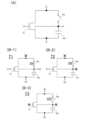
(実施形態1)
本実施形態では、2つのゲートを有する電界効果トランジスタを備える半導体装置の例に
ついて図1を用いて説明する。(Embodiment 1)
In this embodiment, an example of a semiconductor device including a field effect transistor having two gates will be described with reference to FIG.
図1(A)に示す半導体装置は、電界効果トランジスタTrと、スイッチSwと、容量素
子Cpと、を備える。The semiconductor device shown in FIG. 1A includes a field effect transistor Tr, a switch Sw, and a capacitor Cp.
電界効果トランジスタTrは、第1のゲート及び第2のゲートを有する。電界効果トラン
ジスタTrにおける第1のゲート及び第2のゲートは、チャネル形成領域を介して互いに
重畳する。また、電界効果トランジスタTrは、第2のゲートの電位に応じて閾値電圧の
値が制御される。The field effect transistor Tr has a first gate and a second gate. The first gate and the second gate of the field effect transistor Tr overlap each other via a channel formation region. The value of the threshold voltage of the field effect transistor Tr is controlled in response to the potential of the second gate.
電界効果トランジスタTrとしては、エンハンスメント型又はデプレッション型の電界効
果トランジスタを用いることができる。As the field effect transistor Tr, an enhancement type or a depletion type field effect transistor can be used.
スイッチSwは、電界効果トランジスタTrにおけるソース及びドレインの一方と、電界
効果トランジスタTrにおける第2のゲートと、を導通状態にするか否かを制御する機能
を有する。The switch Sw has a function of controlling whether one of the source and the drain of the field effect transistor Tr and the second gate of the field effect transistor Tr are brought into a conductive state.
容量素子Cpは、電界効果トランジスタTrにおける第2のゲートと電界効果トランジス
タTrにおけるソース及びドレインの他方との間の電圧を保持する機能を有する。The capacitance element Cp has a function of holding a voltage between the second gate of the field effect transistor Tr and the other of the source and drain of the field effect transistor Tr.
次に、本実施形態における半導体装置の駆動方法例として図1(A)に示す半導体装置の
駆動方法例について図1(B-1)乃至図1(B-3)を用いて説明する。なお、ここで
は、一例として電界効果トランジスタTrが、デプレッション型のNチャネル型トランジ
スタである場合について説明する。Next, as an example of a method for driving the semiconductor device according to this embodiment, an example of a method for driving the semiconductor device shown in FIG 1A will be described with reference to FIG 1B-1 to FIG 1B-3. Note that, as an example, the case where the field-effect transistor Tr is a depletion-type N-channel transistor will be described here.
図1(A)に示す半導体装置の駆動方法例では、図1(B-1)に示すように、期間T1
において、スイッチSwをオン状態(状態ONともいう)にする。また、電界効果トラン
ジスタTrにおける第1のゲートに電位V1を供給する。また、電界効果トランジスタT
rにおける第2のゲートに電位V2を供給する。また、電界効果トランジスタTrにおけ
るソース及びドレインの他方に電位Vbを供給する。なお、V2の値は、V1-Vbの値
より大きいとする。In the example of the method for driving the semiconductor device shown in FIG. 1A, as shown in FIG.
In this case, the switch Sw is turned on (also referred to as the ON state). A potential V1 is supplied to the first gate of the field effect transistor Tr.
A potential V2 is supplied to the second gate of the field effect transistor Tr, and a potential Vb is supplied to the other of the source and drain of the field effect transistor Tr. The value of V2 is assumed to be greater than the value of V1-Vb.
このとき、電界効果トランジスタTrにおける第2のゲートとドレインが導通状態になり
、電界効果トランジスタTrにおける第2のゲート及びドレインのそれぞれの電位が電位
V2になる。これにより、電位V2に応じて電界効果トランジスタTrの閾値電圧(Vt
hともいう)が負方向にシフトする。At this time, the second gate and drain of the field effect transistor Tr are in a conductive state, and the potentials of the second gate and drain of the field effect transistor Tr become the potential V2. As a result, the threshold voltage (Vt
h) shifts in the negative direction.
例えば、元の電界効果トランジスタTrの閾値電圧をVth0とすると、期間T1におけ
る電界効果トランジスタTrの閾値電圧は、Vth0-ΔVthとなる。このとき、ΔV
thの値は、電位V2の値に応じて決まる。よって、電位V2の値に応じて電界効果トラ
ンジスタTrの閾値電圧の値が変化する。For example, if the threshold voltage of the original field effect transistor Tr is Vth0, the threshold voltage of the field effect transistor Tr during the period T1 is Vth0-ΔVth.
The value of th is determined according to the value of the potential V2. Therefore, the value of the threshold voltage of the field effect transistor Tr changes according to the value of the potential V2.
また、電界効果トランジスタTrにおける第1のゲートとソースの間の電圧(Vgsとも
いう)がV1-Vbになる。このとき、V1-Vbの値は、期間T1における電界効果ト
ランジスタTrの閾値電圧より大きい。このため、電界効果トランジスタTrがオン状態
になる。Furthermore, the voltage (also referred to as Vgs) between the first gate and the source of the field-effect transistor Tr becomes V1-Vb. At this time, the value of V1-Vb is greater than the threshold voltage of the field-effect transistor Tr in the period T1. Therefore, the field-effect transistor Tr is turned on.
次に、期間T2において、スイッチSwをオン状態にする。また、電界効果トランジスタ
Trにおける第1のゲートに電位V1を供給する。また、電界効果トランジスタTrにお
ける第2のゲートを浮遊状態にする。Next, in a period T2, the switch Sw is turned on, a potential V1 is supplied to the first gate of the field effect transistor Tr, and the second gate of the field effect transistor Tr is brought into a floating state.
このとき、電界効果トランジスタTrは、オン状態のままである。よって、電界効果トラ
ンジスタTrにおけるソースとドレインの間に電流が流れることにより、電界効果トラン
ジスタTrにおける第2のゲートの電位が変化する。これにより、電界効果トランジスタ
Trにおける閾値電圧の値が正方向にシフトし、電界効果トランジスタTrにおける閾値
電圧がV1-Vb以上になった時点で電界効果トランジスタTrがオフ状態になる。これ
により、電界効果トランジスタTrの閾値電圧データが得られる。At this time, the field effect transistor Tr remains in the on state. Therefore, a current flows between the source and drain of the field effect transistor Tr, and the potential of the second gate of the field effect transistor Tr changes. As a result, the value of the threshold voltage of the field effect transistor Tr shifts in the positive direction, and when the threshold voltage of the field effect transistor Tr becomes equal to or higher than V1-Vb, the field effect transistor Tr is turned off. In this way, the threshold voltage data of the field effect transistor Tr is obtained.
次に、期間T3において、スイッチSwをオフ状態にする。また、電界効果トランジスタ
Trにおける第1のゲートの電位をV1+Vsigにして電界効果トランジスタTrにお
ける第1のゲートを浮遊状態にする。Vsigは、データ信号の電位である。また、電界
効果トランジスタTrにおける第2のゲートを浮遊状態にする。また、電界効果トランジ
スタTrにおけるソース及びドレインの一方に電位Vaを供給する。Next, in a period T3, the switch Sw is turned off. The potential of the first gate of the field effect transistor Tr is set to V1+Vsig to put the first gate of the field effect transistor Tr into a floating state. Vsig is the potential of the data signal. The second gate of the field effect transistor Tr is put into a floating state. A potential Va is supplied to one of the source and drain of the field effect transistor Tr.
このとき、電界効果トランジスタTrがオン状態になり、電界効果トランジスタTrにお
けるソースとドレインの間に電流が流れる。このとき、電界効果トランジスタTrにおけ
るソース及びドレインの他方の電位を電位Vcとする。At this time, the field effect transistor Tr is turned on, and a current flows between the source and drain of the field effect transistor Tr. At this time, the potential of the other of the source and drain of the field effect transistor Tr is set to a potential Vc.
例えば、電界効果トランジスタTrを飽和領域で動作させる場合、電界効果トランジスタ
Trにおけるソースとドレインの間に流れる電流値(Ids)は、電界効果トランジスタ
Trの閾値電圧に関係なく、第1のゲートに入力されたデータ信号の値に応じて決まる。
よって、例えばVgsがV1-Vbより大きい場合に電界効果トランジスタTrがオン状
態になり、ソースとドレインの間に電流が流れる。For example, when the field effect transistor Tr is operated in the saturation region, the value of the current (Ids) flowing between the source and drain of the field effect transistor Tr is determined according to the value of the data signal input to the first gate, regardless of the threshold voltage of the field effect transistor Tr.
Therefore, for example, when Vgs is greater than V1-Vb, the field effect transistor Tr is turned on, and a current flows between the source and drain.
また、電界効果トランジスタTrの劣化などにより、電界効果トランジスタTrのソース
及びドレインの他方の電位が変化した場合であっても電界効果トランジスタTrにおける
第1のゲート及び第2のゲートが浮遊状態であり、容量素子Cpがあるため、電界効果ト
ランジスタTrにおける第1のゲートとソースの間における電圧の変化を抑制できる。Furthermore, even if the potential of the other of the source and drain of the field effect transistor Tr changes due to deterioration of the field effect transistor Tr or the like, the first gate and the second gate of the field effect transistor Tr are in a floating state, and the capacitance element Cp is present, so that the change in voltage between the first gate and the source of the field effect transistor Tr can be suppressed.
なお、期間T2と期間T3の間に移動度補正期間を設け、電界効果トランジスタTrの移
動度に応じて電界効果トランジスタTrにおける第2のゲートの電位を設定してもよい。
これにより、電界効果トランジスタTrの移動度のばらつきによる影響を抑制できる。Note that a mobility correction period may be provided between the period T2 and the period T3, and the potential of the second gate of the field effect transistor Tr may be set in accordance with the mobility of the field effect transistor Tr.
This makes it possible to suppress the influence of variations in the mobility of the field effect transistor Tr.
以上が本実施形態における半導体装置の駆動方法例の説明である。The above is an explanation of an example of a method for driving a semiconductor device in this embodiment.
図1を用いて説明したように、本実施形態における半導体装置の一例では、閾値電圧デー
タ取得期間(例えば期間T2)を設け、電界効果トランジスタの閾値電圧のデータを予め
取得しておく。これにより、電界効果トランジスタのソースとドレインの間に流れる電流
量を、電界効果トランジスタの閾値電圧に関係なく決められるため、電界効果トランジス
タの閾値電圧のばらつきによる影響を抑制できる。また、電界効果トランジスタの劣化に
よる影響を抑制できる。1, in one example of the semiconductor device of this embodiment, a threshold voltage data acquisition period (e.g., period T2) is provided, and data on the threshold voltage of the field effect transistor is acquired in advance. This allows the amount of current flowing between the source and drain of the field effect transistor to be determined regardless of the threshold voltage of the field effect transistor, thereby suppressing the influence of variations in the threshold voltage of the field effect transistor. In addition, the influence of degradation of the field effect transistor can be suppressed.
また、本実施形態における半導体装置の一例では、チャネル形成領域を介して互いに重畳
する第1のゲート及び第2のゲートを有する電界効果トランジスタを用いる。上記構成に
より、電界効果トランジスタがデプレッション型トランジスタであっても、電界効果トラ
ンジスタの閾値電圧データを取得できる。なぜならば、第2のゲートの電位により電界効
果トランジスタの閾値電圧をシフトさせることができるため、電界効果トランジスタがN
チャネル型トランジスタであり、電界効果トランジスタの元々の閾値電圧が負の値でノー
マリオンであり、且つ電界効果トランジスタにおける第1のゲートとソースの間の電圧が
負の値にならなくても電界効果トランジスタをオフ状態にすることができるからである。
よって、電界効果トランジスタにおけるソースとドレインの間に流れる電流量を、電界効
果トランジスタの閾値電圧に関係なく決められるため、電界効果トランジスタの閾値電圧
のばらつきによる影響を抑制できる。In addition, in one example of the semiconductor device in this embodiment, a field effect transistor having a first gate and a second gate overlapping each other via a channel formation region is used. With the above configuration, even if the field effect transistor is a depletion type transistor, threshold voltage data of the field effect transistor can be acquired. This is because the threshold voltage of the field effect transistor can be shifted by the potential of the second gate, and the field effect transistor is an N type transistor.
This is because the field effect transistor is a channel type transistor, the original threshold voltage of the field effect transistor is a negative value and is normally on, and the field effect transistor can be turned off even if the voltage between the first gate and the source of the field effect transistor does not become a negative value.
Therefore, the amount of current flowing between the source and drain of the field effect transistor can be determined regardless of the threshold voltage of the field effect transistor, so that the influence of variations in the threshold voltage of the field effect transistor can be suppressed.
よって、本実施形態における半導体装置の一例では、電界効果トランジスタにおけるソー
スとドレインの間に流れる電流量を制御できるため、動作不良を抑制できる。Therefore, in the example of the semiconductor device according to this embodiment, the amount of current flowing between the source and drain of the field effect transistor can be controlled, thereby suppressing malfunctions.
(実施形態2)
本実施形態では、2つのゲートを有する電界効果トランジスタを備える発光装置の例につ
いて図2乃至図6を用いて説明する。(Embodiment 2)
In this embodiment, an example of a light emitting device including a field effect transistor having two gates will be described with reference to FIGS.
図2(A)に示す発光装置は、配線151乃至配線158と、電界効果トランジスタ11
1乃至電界効果トランジスタ118と、容量素子121及び容量素子122と、発光素子
(ELともいう)140と、を備える。The light-emitting device shown in FIG. 2A includes
The pixel includes a field-
配線151は、例えばデータ信号を供給するためのデータ信号線としての機能を有する。Wiring 151 functions, for example, as a data signal line for supplying a data signal.
配線152は、例えば電位を供給するための電位供給線としての機能を有する。The
配線153は、例えばパルス信号であるゲート信号を供給するためのゲート信号線として
の機能を有する。The
配線154は、例えばパルス信号であるゲート信号を供給するためのゲート信号線として
の機能を有する。The
配線155は、例えばパルス信号であるゲート信号を供給するためのゲート信号線として
の機能を有する。The
配線156は、例えば電位を供給するための電位供給線としての機能を有する。The
配線157は、例えば電位を供給するための電位供給線としての機能を有する。The
配線158は、例えば電位を供給するための電位供給線としての機能を有する。The
電界効果トランジスタ111におけるソース及びドレインの一方は、配線151に電気的
に接続される。また、電界効果トランジスタ111におけるゲートは、配線153に電気
的に接続される。One of the source and the drain of the field-
電界効果トランジスタ112におけるソース及びドレインの一方は、電界効果トランジス
タ111におけるソース及びドレインの他方に電気的に接続される。また、電界効果トラ
ンジスタ112におけるゲートは、配線154に電気的に接続される。One of the source and the drain of the
容量素子121における一対の電極の一方は、電界効果トランジスタ111におけるソー
ス及びドレインの他方に電気的に接続される。One of a pair of electrodes of the
電界効果トランジスタ113は、チャネル形成領域を介して互いに重畳する第1のゲート
及び第2のゲートを有する。電界効果トランジスタ113における第1のゲートは、電界
効果トランジスタ112におけるソース及びドレインの他方に電気的に接続される。The
電界効果トランジスタ114におけるソース及びドレインの一方は、電界効果トランジス
タ113におけるソース及びドレインの一方に電気的に接続される。また、電界効果トラ
ンジスタ114におけるソース及びドレインの他方は、電界効果トランジスタ113にお
ける第2のゲートに電気的に接続される。また、電界効果トランジスタ114におけるゲ
ートは、配線153に電気的に接続される。One of the source and the drain of the
容量素子122における一対の電極の一方は、電界効果トランジスタ113における第2
のゲートに電気的に接続される。また、容量素子122における一対の電極の他方は、電
界効果トランジスタ113におけるソース及びドレインの他方に電気的に接続される。One of the pair of electrodes of the
The other of the pair of electrodes of the
電界効果トランジスタ115におけるソース及びドレインの一方は、配線152に電気的
に接続される。また、電界効果トランジスタ115におけるソース及びドレインの他方は
、電界効果トランジスタ113におけるソース及びドレインの一方に電気的に接続される
。また、電界効果トランジスタ115におけるゲートは、配線154に電気的に接続され
る。One of the source and the drain of the
電界効果トランジスタ116におけるソース及びドレインの一方は、配線156に電気的
に接続される。また、電界効果トランジスタ116におけるソース及びドレインの他方は
、電界効果トランジスタ113における第1のゲートに電気的に接続される。また、電界
効果トランジスタ116におけるゲートは、配線153に電気的に接続される。One of the source and the drain of the
電界効果トランジスタ117におけるソース及びドレインの一方は、配線157に電気的
に接続される。また、電界効果トランジスタ117におけるソース及びドレインの他方は
、容量素子121における一対の電極の他方及び容量素子122における一対の電極の他
方に電気的に接続される。また、電界効果トランジスタ117におけるゲートは、配線1
53に電気的に接続される。One of the source and the drain of the
53 is electrically connected to the
電界効果トランジスタ118におけるソース及びドレインの一方は、配線158に電気的
に接続される。また、電界効果トランジスタ118におけるソース及びドレインの他方は
、電界効果トランジスタ113における第2のゲートに電気的に接続される。また、電界
効果トランジスタ118におけるゲートは、配線155に電気的に接続される。One of the source and the drain of the
発光素子140におけるアノード及びカソードの一方は、電界効果トランジスタ113に
おけるソース及びドレインの他方に電気的に接続される。発光素子140としては、例え
ばエレクトロルミネセンス素子(EL素子ともいう)を用いることができる。One of the anode and the cathode of the light-emitting
さらに、図2(B)に示す発光装置は、図2(A)に示す発光装置の電界効果トランジス
タ113及び電界効果トランジスタ117の接続関係が異なる構成である。Furthermore, the light-emitting device shown in FIG. 2B has a different connection relationship between the field-
図2(B)に示す発光装置において、電界効果トランジスタ113におけるソース及びド
レインの他方は、電界効果トランジスタ112におけるソース及びドレインの他方に電気
的に接続される。また、電界効果トランジスタ113における第1のゲートは、容量素子
121における一対の電極の他方に電気的に接続される。また、電界効果トランジスタ1
17におけるソース及びドレインの他方は、電界効果トランジスタ112におけるソース
及びドレインの他方、及び容量素子122における一対の電極の他方に電気的に接続され
る。In the light-emitting device shown in FIG. 2B , the other of the source and the drain of the field-
The other of the source and drain of the transistor 17 is electrically connected to the other of the source and drain of the
また、図2(C)に示す発光装置は、図2(B)に示す発光装置の電界効果トランジスタ
116の接続関係が異なり、配線156が無い構成である。2C is different from the light-emitting device shown in FIG. 2B in that the field-
図2(C)に示す発光装置において、電界効果トランジスタ116におけるソース及びド
レインの一方は、電界効果トランジスタ113における第1のゲートに電気的に接続され
る。また、電界効果トランジスタ116におけるソース及びドレインの他方は、容量素子
122における一対の電極の他方に電気的に接続される。また、電界効果トランジスタ1
13は、エンハンスメント型トランジスタでもよい。In the light-emitting device shown in FIG. 2C, one of the source and the drain of the field-
13 may be an enhancement type transistor.
図2(C)に示す構成にすることにより、配線の数を少なくできる。By using the configuration shown in Figure 2 (C), the number of wires can be reduced.
また、図3(A)に示す発光装置は、図2(A)に示す発光装置に加え、配線159及び
配線160を備え、電界効果トランジスタ111及び電界効果トランジスタ117の接続
関係が異なり、電界効果トランジスタ112が無い構成である。In addition to the configuration of the light-emitting device shown in FIG. 2A, the light-emitting device shown in FIG. 3A includes a
図3(A)に示す発光装置において、電界効果トランジスタ111におけるゲートは、配
線159に電気的に接続される。また、電界効果トランジスタ113における第1のゲー
トは、電界効果トランジスタ111におけるソース及びドレインの他方に電気的に接続さ
れる。また、電界効果トランジスタ117におけるゲートは、配線160に電気的に接続
される。3A , a gate of the
図3(B)に示す発光装置は、図3(A)に示す発光装置の容量素子121の接続関係が
異なる構成である。The light-emitting device shown in FIG. 3B has a different structure from the light-emitting device shown in FIG. 3A in terms of the connection relationship of the
図3(B)に示す発光装置において、容量素子121における一対の電極の他方は、電界
効果トランジスタ111におけるソース及びドレインの他方に電気的に接続される。In the light-emitting device shown in FIG. 3B, the other of the pair of electrodes of the
図3(C)に示す発光装置は、図3(B)に示す発光装置の電界効果トランジスタ116
の接続関係が異なり、配線156が無い構成である。The light-emitting device shown in FIG. 3C has a field-
The connection relationship is different, and the
図3(C)に示す発光装置において、電界効果トランジスタ116におけるソース及びド
レインの一方は、電界効果トランジスタ113における第1のゲートに電気的に接続され
る。また、電界効果トランジスタ116におけるソース及びドレインの他方は、容量素子
122における一対の電極の他方に電気的に接続される。電界効果トランジスタ113は
、エンハンスメント型トランジスタでもよい。3C , one of the source and the drain of the
図3(C)に示す構成にすることにより、配線の数を少なくできる。By using the configuration shown in Figure 3(C), the number of wiring can be reduced.
また、図3(A)乃至図3(C)に示す構成にすることにより、電界効果トランジスタの
数を少なくすることができる。In addition, by using the structures shown in FIGS. 3A to 3C, the number of field effect transistors can be reduced.
また、発光素子140に印加される電圧を調整するための容量素子を備える発光装置の例
について、図4を用いて説明する。An example of a light-emitting device including a capacitor for adjusting a voltage applied to the light-emitting
図4(A)に示す発光装置は、図2(A)に示す発光装置の構成に加え、容量素子123
を備える。The light-emitting device shown in FIG. 4A has the structure of the light-emitting device shown in FIG. 2A, and further has a
Equipped with.
図4(A)に示す発光装置において、容量素子123における一対の電極の一方は、発光
素子140におけるアノード及びカソードの一方に電気的に接続される。また、容量素子
123における一対の電極の一方には、基準電位が与えられる。4A, one of a pair of electrodes in a
また、図4(B)に示す発光装置は、図2(B)に示す発光装置の構成に加え、容量素子
123を備える構成である。容量素子123の接続関係は、図4(A)に示す発光装置と
同じである。4B includes a
また、図4(C)に示す発光装置は、図2(C)に示す発光装置の構成に加え、容量素子
123を備える構成である。容量素子123の接続関係は、図4(A)に示す発光装置と
同じである。4C includes a
なお、図4(A)乃至図4(C)に示す発光装置に限定されず、例えば図3(A)乃至図
3(C)に示す発光装置の構成に加えて容量素子を設けてもよい。Note that the light-emitting device is not limited to the light-emitting devices shown in FIGS. 4A to 4C. For example, a capacitor may be provided in addition to the structure of the light-emitting device shown in FIGS.
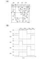
次に、本実施形態における発光装置の駆動方法例について図5及び図6を用いて説明する
。Next, an example of a method for driving the light emitting device in this embodiment will be described with reference to FIGS.
本実施形態における発光装置の駆動方法例として、図5(A)に示す発光装置の駆動方法
例について、図5(B)のタイミングチャートを用いて説明する。図5(A)に示す発光
装置は、図2(A)に示す発光装置の発光素子140が発光ダイオードであり、電界効果
トランジスタ111乃至電界効果トランジスタ118のそれぞれがNチャネル型トランジ
スタである場合の発光装置である。このとき、発光素子140である発光ダイオードにお
けるアノードは、容量素子122における一対の電極の他方に電気的に接続される。また
、発光素子140である発光ダイオードにおけるカソードには電位Vxが与えられる。As an example of a method for driving the light-emitting device in this embodiment, an example of a method for driving the light-emitting device shown in Fig. 5A will be described with reference to a timing chart in Fig. 5B. The light-emitting device shown in Fig. 5A is a light-emitting device in which the light-emitting
図5(A)に示す発光装置の駆動方法例では、図5(B)に示すように、期間T11にお
いて、配線153を介してハイレベル(VHともいう)の信号を入力し、配線154を介
してローレベル(VLともいう)の信号を入力し、配線155を介してハイレベルの信号
を入力する。また、配線156に電位V11を供給し、配線157に電位V12を供給し
、配線158に電位V13を供給する。このとき、電位V11と電位V12の電位差は、
電界効果トランジスタ113の閾値電圧(Vth113ともいう)より大きいとする。ま
た、電位V12は、電位Vxより小さいとする。In the example of a method for driving a light-emitting device shown in FIG. 5A, as shown in FIG. 5B, in a period T11, a high-level (also referred to as VH) signal is input through a
The potential V12 is assumed to be higher than the threshold voltage (also referred to as Vth113) of the
このとき、電界効果トランジスタ111、電界効果トランジスタ114、電界効果トラン
ジスタ116、電界効果トランジスタ117、及び電界効果トランジスタ118がオン状
態になり、電界効果トランジスタ112、及び電界効果トランジスタ115がオフ状態に
なる。At this time, the
また、電界効果トランジスタ113における第2のゲートとドレインが導通状態になり、
電界効果トランジスタ113における第2のゲート及びドレインのそれぞれの電位が電位
V13になる。これにより、電位V13に応じて電界効果トランジスタ113の閾値電圧
が負方向にシフトする。In addition, the second gate and the drain of the
The potentials of the second gate and the drain of the
また、電界効果トランジスタ113における第1のゲートとソースの間の電圧(Vgs1
13ともいう)がV11-V12になる。V11-V12の値は、このときの電界効果ト
ランジスタ113の閾値電圧より大きい。このため、電界効果トランジスタ113がオン
状態になる。In addition, the voltage between the first gate and the source of the field effect transistor 113 (Vgs1
13) becomes V11-V12. The value of V11-V12 is greater than the threshold voltage of the
次に、期間T12において、配線151を介してデータ信号を入力し、配線153を介し
てハイレベルの信号を入力し、配線154を介してローレベルの信号を入力し、配線15
5を介してローレベルの信号を入力する。また、配線156に電位V11を供給し、配線
157に電位V12を供給する。Next, in a period T12, a data signal is input through the
A low-level signal is input via the
このとき、電界効果トランジスタ111、電界効果トランジスタ114、電界効果トラン
ジスタ116、及び電界効果トランジスタ117がオン状態になり、電界効果トランジス
タ112、電界効果トランジスタ115、及び電界効果トランジスタ118がオフ状態に
なる。At this time, the
また、電界効果トランジスタ113は、オン状態のままである。よって、電界効果トラン
ジスタ113におけるソースとドレインの間に電流が流れることにより、電界効果トラン
ジスタ113における第2のゲートの電位が変化する。これにより、電界効果トランジス
タ113における閾値電圧の値が正方向にシフトし、電界効果トランジスタ113におけ
る閾値電圧がV11-V12以上になった時点で電界効果トランジスタ113がオフ状態
になる。これにより、電界効果トランジスタ113の閾値電圧データを得る。Moreover, the
また、容量素子121における一対の電極の一方の電位が配線151を介して入力される
データ信号の電位(Vsig)となる。Further, the potential of one of the pair of electrodes of the
次に、期間T13において、配線153を介してローレベルの信号を入力し、配線154
を介してハイレベルの信号を入力し、配線155を介してローレベルの信号を入力する。
また、配線152に電位Vddを供給する。なお、電位Vddの値は、電位V11より高
いとする。また、期間T13において、配線153を介してローレベルの信号を入力した
後に配線154を介してハイレベルの信号を入力しているが、これに限定されない。Next, in a period T13, a low-level signal is input through the
A high-level signal is input via the
Further, a potential Vdd is supplied to the
このとき、電界効果トランジスタ112及び電界効果トランジスタ115がオン状態にな
り、電界効果トランジスタ111、電界効果トランジスタ114、電界効果トランジスタ
116、電界効果トランジスタ117、及び電界効果トランジスタ118がオフ状態にな
る。At this time, the
さらに、電界効果トランジスタ113における第1のゲートの電位がデータ信号の値に応
じて変化する。これにより、電界効果トランジスタ113がオン状態になり、電界効果ト
ランジスタ113におけるソースとドレインの間に電流が流れる。Furthermore, the potential of the first gate of the
さらに、発光素子140である発光ダイオードにおけるアノードとカソードの間に電流が
流れることにより発光素子140である発光ダイオードが発光する。Furthermore, when a current flows between the anode and cathode of the light emitting diode, which is the
例えば、電界効果トランジスタ113を飽和領域で動作させる場合、電界効果トランジス
タ113におけるソースとドレインの間に流れる電流値(Ids)は、電界効果トランジ
スタ113の閾値電圧に関係なく、第1のゲートに入力されたデータ信号の値に応じて決
まる。よって、例えばVgs113がV11-V12より大きい場合に電界効果トランジ
スタ113がオン状態になり、ソースとドレインの間に電流が流れる。For example, when the
また、電界効果トランジスタ113の劣化などにより、電界効果トランジスタ113のソ
ース及びドレインの他方の電位が変化した場合であっても電界効果トランジスタ113に
おける第1のゲート及び第2のゲートが浮遊状態であり、容量素子121及び容量素子1
22があるため、電界効果トランジスタ113における第1のゲートとソースの間におけ
る電圧の値の変化を抑制できる。In addition, even if the potential of the other of the source and drain of the
22, the change in the value of the voltage between the first gate and the source of the
なお、期間T12と期間T13の間に移動度補正期間を設け、電界効果トランジスタ11
3の移動度に応じて電界効果トランジスタ113における第2のゲートの電位を設定して
もよい。これにより、電界効果トランジスタ113の移動度のばらつきによる影響を抑制
できる。A mobility correction period is provided between the period T12 and the period T13, and the field effect transistor 11
The potential of the second gate of the
以上が図5(A)に示す発光装置の駆動方法例の説明である。The above is an explanation of an example of a method for driving the light-emitting device shown in Figure 5 (A).
なお、図5(A)に示す半導体装置の電界効果トランジスタ111乃至電界効果トランジ
スタ118の一つ又は複数をPチャネル型トランジスタとしてもよい。Note that one or more of the field-
次に、本実施形態における発光装置の駆動方法例として、図6(A)に示す発光装置の駆
動方法例について、図6(B)のタイミングチャートを用いて説明する。図6(A)に示
す発光装置は、図3(A)に示す発光装置の発光素子140が発光ダイオードであり、電
界効果トランジスタ111乃至電界効果トランジスタ118のそれぞれがNチャネル型ト
ランジスタである場合の発光装置である。このとき、発光素子140である発光ダイオー
ドにおけるアノードは、容量素子122における一対の電極の他方に電気的に接続される
。また、発光素子140である発光ダイオードにおけるカソードには電位Vxが与えられ
る。Next, as an example of a method for driving the light-emitting device in this embodiment, an example of a method for driving the light-emitting device shown in Fig. 6A will be described with reference to a timing chart in Fig. 6B. The light-emitting device shown in Fig. 6A is a light-emitting device in which the light-emitting
図6(A)に示す発光装置の駆動方法例では、図6(B)に示すように、期間T21にお
いて、配線153を介してハイレベルの信号を入力し、配線154を介してローレベルの
信号を入力し、配線155を介してハイレベルの信号を入力し、配線159を介してロー
レベルの信号を入力し、配線160を介してハイレベルの信号を入力する。また、配線1
56に電位V11を供給し、配線157に電位V12を供給し、配線158に電位V13
を供給する。このとき、電位V11と電位V12の電位差は、電界効果トランジスタ11
3の閾値電圧より大きいとする。また、電位V12は、電位Vxより小さいとする。In the example of the method for driving the light-emitting device shown in FIG. 6A, as shown in FIG. 6B, in a period T21, a high-level signal is input through the
A potential V11 is supplied to the wiring 56, a potential V12 is supplied to the
At this time, the potential difference between the potential V11 and the potential V12 is
It is assumed that the potential V12 is larger than the threshold voltage of the potential Vx.
このとき、電界効果トランジスタ114、電界効果トランジスタ116、電界効果トラン
ジスタ117、及び電界効果トランジスタ118がオン状態になり、電界効果トランジス
タ111、及び電界効果トランジスタ115がオフ状態になる。At this time, the
また、電界効果トランジスタ113における第2のゲートとドレインが導通状態になり、
電界効果トランジスタ113における第2のゲート及びドレインのそれぞれの電位が電位
V13になる。これにより、電位V13に応じて電界効果トランジスタ113の閾値電圧
が負方向にシフトする。In addition, the second gate and the drain of the
The potentials of the second gate and the drain of the
また、電界効果トランジスタ113におけるゲートとソースの間の電圧がV11-V12
になる。V11-V12の値は、このときの電界効果トランジスタ113の閾値電圧より
大きい。このため、電界効果トランジスタ113がオン状態になる。In addition, the voltage between the gate and source of the
At this time, the value of V11-V12 is greater than the threshold voltage of the
また、期間T22において、配線153を介してハイレベルの信号を入力し、配線154
を介してローレベルの信号を入力し、配線155を介してローレベルの信号を入力し、配
線159を介してローレベルの信号を入力し、配線160を介してハイレベルの信号を入
力する。また、配線156に電位V11を供給し、配線157に電位V12を供給する。In addition, in the period T22, a high-level signal is input through the
A low-level signal is input through the
このとき、電界効果トランジスタ114、電界効果トランジスタ116、及び電界効果ト
ランジスタ117がオン状態になり、電界効果トランジスタ111、電界効果トランジス
タ115、及び電界効果トランジスタ118がオフ状態になる。At this time, the
また、電界効果トランジスタ113は、オン状態のままである。よって、電界効果トラン
ジスタ113におけるソースとドレインの間に電流が流れることにより、電界効果トラン
ジスタ113における第2のゲートの電位が変化する。これにより、電界効果トランジス
タ113における閾値電圧の値が正方向にシフトし、電界効果トランジスタ113におけ
る閾値電圧がV11-V12以上になった時点で電界効果トランジスタ113がオフ状態
になる。これにより、電界効果トランジスタ113の閾値電圧データを得る。Moreover, the
次に、期間T23において、配線153を介してローレベルの信号を入力し、配線154
を介してローレベルの信号を入力し、配線155を介してローレベルの信号を入力し、配
線159を介してハイレベルの信号を入力し、配線160を介してローレベルの信号を入
力する。また、配線151を介してデータ信号を入力する。Next, in a period T23, a low-level signal is input through the
A low-level signal is input through the
このとき、電界効果トランジスタ111がオン状態になり、電界効果トランジスタ114
、電界効果トランジスタ115、電界効果トランジスタ116、電界効果トランジスタ1
17、及び電界効果トランジスタ118がオフ状態になる。At this time, the
,
17 and
このとき、電界効果トランジスタ113における第1のゲートの電位がデータ信号(Vs
ig)の電位に応じて変化する。At this time, the potential of the first gate of the
ig) changes depending on the potential.
次に、期間T24において、配線153を介してローレベルの信号を入力し、配線154
を介してハイレベルの信号を入力し、配線155を介してローレベルの信号を入力し、配
線159を介してローレベルの信号を入力し、配線160を介してローレベルの信号を入
力する。また、配線152を介して電位Vddを供給する。なお、電位Vddの値は、電
位V11より高いとする。Next, in a period T24, a low-level signal is input through the
A high-level signal is input through the
このとき、電界効果トランジスタ115がオン状態になり、電界効果トランジスタ111
、電界効果トランジスタ114、電界効果トランジスタ116、電界効果トランジスタ1
17、及び電界効果トランジスタ118がオフ状態になる。At this time, the
,
17 and
また、電界効果トランジスタ113がオン状態になり、電界効果トランジスタ113にお
けるソースとドレインの間に電流が流れる。Furthermore, the
さらに、発光素子140である発光ダイオードにおけるアノードとカソードの間に電流が
流れることにより発光素子140である発光ダイオードが発光する。Furthermore, when a current flows between the anode and cathode of the light emitting diode, which is the
例えば、電界効果トランジスタ113を飽和領域で動作させる場合、電界効果トランジス
タ113におけるソースとドレインの間に流れる電流値(Ids)は、電界効果トランジ
スタ113の閾値電圧に関係なく、第1のゲートに入力されたデータ信号(Vsig)の
値に応じて決まる。よって、例えばVgs113がV11-V12より大きい場合に電界
効果トランジスタ113がオン状態になり、ソースとドレインの間に電流が流れる。For example, when the
また、電界効果トランジスタ113の劣化などにより、電界効果トランジスタ113にお
けるソース及びドレインの他方の電位が変化した場合であっても電界効果トランジスタ1
13における第1のゲート及び第2のゲートが浮遊状態であり、容量素子121及び容量
素子122があるため、電界効果トランジスタ113における第1のゲートとソースの間
における電圧の値の変化を抑制できる。In addition, even if the potential of the other of the source and drain of the
Since the first gate and the second gate of the
なお、期間T23と期間T24の間に移動度補正期間を設け、電界効果トランジスタ11
3の移動度に応じて電界効果トランジスタ113における第2のゲートの電位を設定して
もよい。これにより、電界効果トランジスタ113の移動度のばらつきによる影響を抑制
できる。A mobility correction period is provided between the period T23 and the period T24, and the field effect transistor 11
The potential of the second gate of the
なお、図6(A)に示す半導体装置の電界効果トランジスタ111乃至電界効果トランジ
スタ118の一つ又は複数をPチャネル型トランジスタとしてもよい。Note that one or more of the field-
以上が図6(A)に示す発光装置の駆動方法例の説明である。The above is an explanation of an example of a method for driving the light-emitting device shown in Figure 6 (A).
図5及び図6を用いて説明したように、本実施形態における発光装置の一例では、閾値電
圧データ取得期間を設け、電界効果トランジスタの閾値電圧のデータを予め取得しておく
。これにより、電界効果トランジスタのソースとドレインの間に流れる電流量を、電界効
果トランジスタの閾値電圧に関係なく決めることができるため、電界効果トランジスタの
閾値電圧のばらつきによる影響を抑制できる。また、電界効果トランジスタの劣化による
影響を抑制できる。As described with reference to Figures 5 and 6, in one example of the light emitting device of this embodiment, a threshold voltage data acquisition period is set, and data on the threshold voltage of the field effect transistor is acquired in advance. This allows the amount of current flowing between the source and drain of the field effect transistor to be determined regardless of the threshold voltage of the field effect transistor, thereby suppressing the influence of variations in the threshold voltage of the field effect transistor. In addition, the influence of deterioration of the field effect transistor can be suppressed.
また、本実施形態における発光装置の一例では、第1のゲート及び第2のゲートを有する
電界効果トランジスタを用いる。上記構成により、電界効果トランジスタがデプレッショ
ン型トランジスタであっても、電界効果トランジスタの閾値電圧データを取得できる。な
ぜならば、第2のゲートの電位により電界効果トランジスタの閾値電圧をシフトさせるこ
とができるため、電界効果トランジスタがNチャネル型トランジスタであり、電界効果ト
ランジスタの元々の閾値電圧が負の値でノーマリオンであり、且つ電界効果トランジスタ
における第1のゲートとソースの間の電圧が負の値にならなくても電界効果トランジスタ
をオフ状態にすることができるからである。よって、電界効果トランジスタにおけるソー
スとドレインの間に流れる電流量を、電界効果トランジスタの閾値電圧に関係なく決めら
れるため、電界効果トランジスタの閾値電圧のばらつきによる影響を抑制できる。In addition, in one example of the light-emitting device in this embodiment, a field effect transistor having a first gate and a second gate is used. With the above configuration, even if the field effect transistor is a depletion type transistor, the threshold voltage data of the field effect transistor can be acquired. This is because the threshold voltage of the field effect transistor can be shifted by the potential of the second gate, and the field effect transistor can be turned off even if the field effect transistor is an N-channel transistor, the original threshold voltage of the field effect transistor is a negative value and is normally on, and the voltage between the first gate and the source of the field effect transistor does not become a negative value. Therefore, the amount of current flowing between the source and drain of the field effect transistor can be determined regardless of the threshold voltage of the field effect transistor, so that the influence of the variation in the threshold voltage of the field effect transistor can be suppressed.
よって、本実施形態における発光装置の一例では、電界効果トランジスタにおけるソース
とドレインの間に流れる電流量を制御できるため、動作不良を抑制できる。Therefore, in the example of the light emitting device according to this embodiment, the amount of current flowing between the source and drain of the field effect transistor can be controlled, thereby suppressing malfunctions.
(実施形態3)
本実施形態では、駆動回路を備える発光装置の構成例について図7を用いて説明する。(Embodiment 3)
In this embodiment, a configuration example of a light emitting device including a driver circuit will be described with reference to FIG.
図7に示す半導体装置は、第1の駆動回路901と、第2の駆動回路902と、複数の発
光回路910と、を備える。The semiconductor device shown in FIG. 7 includes a
第1の駆動回路901は、発光回路910の発光動作を制御する機能を有する。The
第1の駆動回路901は、例えばシフトレジスタなどを用いて構成される。The
第2の駆動回路902は、発光回路910の発光動作を制御する機能を有する。The
第2の駆動回路902は、例えばシフトレジスタ、アナログスイッチなどを用いて構成さ
れる。The
複数の発光回路910は、発光部900において行列方向に配列される。発光回路910
としては、上記実施形態2に示す発光装置の構成を適用することができる。このとき、実
施形態2に示す発光装置における電界効果トランジスタのゲートに電気的に接続された配
線には、第1の駆動回路901から信号が供給される。また、実施形態2に示す発光装置
におけるデータ信号が入力される配線には、第2の駆動回路902からデータ信号が供給
される。The plurality of
As the light-emitting device, the configuration of the light-emitting device shown in the above-described
なお、発光回路910と同一基板上に第1の駆動回路901を設けてもよい。The
以上が図7に示す発光装置の構成例の説明である。The above is an explanation of the configuration example of the light-emitting device shown in Figure 7.
図7を用いて説明したように、本実施形態における発光装置の一例では、第1の駆動回路
及び第2の駆動回路により発光回路の発光動作を制御することができる。As described with reference to FIG. 7, in one example of the light emitting device in this embodiment, the light emitting operation of the light emitting circuit can be controlled by the first drive circuit and the second drive circuit.
(実施形態4)
本実施形態では、上記実施形態の半導体装置又は発光装置における電界効果トランジスタ
の例について説明する。(Embodiment 4)
In this embodiment, an example of a field effect transistor in the semiconductor device or light emitting device of the above embodiment will be described.
本実施形態における電界効果トランジスタの構造例について、図8を用いて説明する。An example of the structure of a field effect transistor in this embodiment is described with reference to Figure 8.
図8(A)に示す電界効果トランジスタは、被素子形成層400_Aの上に、導電層40
1_Aと、絶縁層402_Aと、半導体層403_Aと、導電層405a_Aと、導電層
405b_Aと、絶縁層406と、を含む。The field effect transistor shown in FIG. 8A has a conductive layer 40 on an element formation layer 400_A.
The
また、図8(B)に示す電界効果トランジスタは、被素子形成層400_Bの上に、導電
層401_Bと、絶縁層402_Bと、領域404a及び領域404bを含む半導体層4
03_Bと、導電層405a_Bと、導電層405b_Bと、絶縁層407と、を含む。In addition, the field effect transistor shown in FIG. 8B includes a conductive layer 401_B, an insulating layer 402_B, and a semiconductor layer 404 including a
03_B, a conductive layer 405a_B, a conductive layer 405b_B, and an insulating
さらに、図8(A)及び図8(B)に示す各構成要素について説明する。Furthermore, each component shown in Figures 8(A) and 8(B) will be explained.
被素子形成層400_A及び被素子形成層400_Bとしては、例えば絶縁層、又は絶縁
表面を有する基板などを用いることができる。As the element formation layer 400_A and the element formation layer 400_B, for example, an insulating layer or a substrate having an insulating surface can be used.
導電層401_A及び導電層401_Bのそれぞれは、電界効果トランジスタのゲートと
しての機能を有する。なお、電界効果トランジスタのゲートとしての機能を有する層をゲ
ート電極又はゲート配線ともいう。Each of the conductive layers 401_A and 401_B functions as a gate of a field-effect transistor. Note that a layer having a function as a gate of a field-effect transistor is also referred to as a gate electrode or a gate wiring.
導電層401_A及び導電層401_Bとしては、例えばモリブデン、マグネシウム、チ
タン、クロム、タンタル、タングステン、アルミニウム、銅、ネオジム、若しくはスカン
ジウムなどの金属材料、又はこれらを主成分とする合金材料の層(単層又は積層)を用い
ることができる。The conductive layer 401_A and the conductive layer 401_B can be, for example, a layer (single layer or stack) of a metal material such as molybdenum, magnesium, titanium, chromium, tantalum, tungsten, aluminum, copper, neodymium, or scandium, or an alloy material containing any of these as its main component.
絶縁層402_A及び絶縁層402_Bのそれぞれは、電界効果トランジスタのゲート絶
縁層としての機能を有する。Each of the insulating layer 402_A and the insulating layer 402_B functions as a gate insulating layer of a field effect transistor.
絶縁層402_A及び絶縁層402_Bとしては、例えば酸化シリコン、窒化シリコン、
酸化窒化シリコン、窒化酸化シリコン、酸化アルミニウム、窒化アルミニウム、酸化窒化
アルミニウム、窒化酸化アルミニウム、酸化ハフニウム、又は酸化ランタンなどの材料の
層(単層又は積層)を用いることができる。The insulating layer 402_A and the insulating layer 402_B may be, for example, silicon oxide, silicon nitride,
A layer (single layer or stack) of a material such as silicon oxynitride, silicon nitride oxide, aluminum oxide, aluminum nitride, aluminum oxynitride, aluminum nitride oxide, hafnium oxide, or lanthanum oxide can be used.
また、絶縁層402_A及び絶縁層402_Bとしては、例えば元素周期表における第1
3族元素及び酸素元素を含む材料の絶縁層を用いることもできる。The insulating layer 402_A and the insulating layer 402_B may be, for example, a material selected from the group consisting of the first group of the periodic table of elements.
An insulating layer of a material containing a
第13族元素及び酸素元素を含む材料としては、例えば酸化ガリウム、酸化アルミニウム
、酸化アルミニウムガリウム、酸化ガリウムアルミニウムなどが挙げられる。なお、酸化
アルミニウムガリウムとは、ガリウムの含有量(原子%)よりアルミニウムの含有量(原
子%)が多い物質のことをいい、酸化ガリウムアルミニウムとは、ガリウムの含有量(原
子%)がアルミニウムの含有量(原子%)より多い物質のことをいう。Examples of materials containing a Group 13 element and an oxygen element include gallium oxide, aluminum oxide, aluminum gallium oxide, gallium aluminum oxide, etc. Aluminum gallium oxide refers to a substance in which the aluminum content (atomic %) is greater than the gallium content (atomic %), and gallium aluminum oxide refers to a substance in which the gallium content (atomic %) is greater than the aluminum content (atomic %).
半導体層403_A及び半導体層403_Bのそれぞれは、電界効果トランジスタのチャ
ネルが形成される層(チャネル形成層ともいう)、すなわちチャネル形成領域を有する層
としての機能を有する。半導体層403_A及び半導体層403_Bに適用可能な半導体
としては、例えば元素周期表における第14族の元素(シリコンなど)を含有する半導体
を用いることができる。例えば、シリコンの半導体層は、単結晶半導体層、多結晶半導体
層、微結晶半導体層、又は非晶質半導体層であってもよい。Each of the semiconductor layer 403_A and the semiconductor layer 403_B functions as a layer in which a channel of a field effect transistor is formed (also referred to as a channel formation layer), that is, a layer having a channel formation region. As a semiconductor applicable to the semiconductor layer 403_A and the semiconductor layer 403_B, for example, a semiconductor containing an element of Group 14 in the periodic table (such as silicon) can be used. For example, the silicon semiconductor layer may be a single crystal semiconductor layer, a polycrystalline semiconductor layer, a microcrystalline semiconductor layer, or an amorphous semiconductor layer.
また、半導体層403_A及び半導体層403_Bに適用可能な半導体としては、例えば
シリコンよりバンドギャップが広く、例えば2eV以上、好ましくは2.5eV以上、よ
り好ましくは3eV以上である半導体を用いることができる。例えば、半導体層403_
A及び半導体層403_Bに適用可能な半導体としては、In系酸化物(例えば酸化イン
ジウムなど)、Sn系酸化物(例えば酸化スズなど)、又はZn系酸化物(例えば酸化亜
鉛など)などの金属酸化物などの酸化物半導体を用いることができる。As a semiconductor applicable to the semiconductor layer 403_A and the semiconductor layer 403_B, for example, a semiconductor having a band gap wider than that of silicon, for example, 2 eV or more, preferably 2.5 eV or more, more preferably 3 eV or more, can be used.
As a semiconductor applicable to the semiconductor layer 403_A and the semiconductor layer 403_B, an oxide semiconductor such as a metal oxide such as an In-based oxide (e.g., indium oxide), an Sn-based oxide (e.g., tin oxide), or a Zn-based oxide (e.g., zinc oxide) can be used.
また、上記金属酸化物としては、例えば、四元系金属酸化物、三元系金属酸化物、二元系
金属酸化物などの金属酸化物を用いることもできる。なお、上記酸化物半導体として適用
可能な金属酸化物は、特性のばらつきを減らすためのスタビライザーとしてガリウムを含
んでいてもよい。また、上記酸化物半導体として適用可能な金属酸化物は、上記スタビラ
イザーとしてスズを含んでいてもよい。また、上記酸化物半導体として適用可能な金属酸
化物は、上記スタビライザーとしてハフニウムを含んでいてもよい。また、上記酸化物半
導体として適用可能な金属酸化物は、上記スタビライザーとしてアルミニウムを含んでい
てもよい。また、上記酸化物半導体として適用可能な金属酸化物は、上記スタビライザー
として、ランタノイドである、ランタン、セリウム、プラセオジム、ネオジム、サマリウ
ム、ユウロピウム、ガドリニウム、テルビウム、ジスプロシウム、ホルミウム、エルビウ
ム、ツリウム、イッテルビウム、及びルテチウムの一つ又は複数を含んでいてもよい。ま
た、上記酸化物半導体として適用可能な金属酸化物は、酸化シリコンを含んでいてもよい
。In addition, as the metal oxide, for example, a metal oxide such as a quaternary metal oxide, a ternary metal oxide, or a binary metal oxide can be used. The metal oxide applicable as the oxide semiconductor may contain gallium as a stabilizer for reducing the variation in characteristics. The metal oxide applicable as the oxide semiconductor may contain tin as the stabilizer. The metal oxide applicable as the oxide semiconductor may contain hafnium as the stabilizer. The metal oxide applicable as the oxide semiconductor may contain aluminum as the stabilizer. The metal oxide applicable as the oxide semiconductor may contain one or more of the following lanthanoids as the stabilizer: lanthanum, cerium, praseodymium, neodymium, samarium, europium, gadolinium, terbium, dysprosium, holmium, erbium, thulium, ytterbium, and lutetium. The metal oxide applicable as the oxide semiconductor may contain silicon oxide.
例えば、四元系金属酸化物としては、例えばIn-Sn-Ga-Zn系酸化物、In-H
f-Ga-Zn系酸化物、In-Al-Ga-Zn系酸化物、In-Sn-Al-Zn系
酸化物、In-Sn-Hf-Zn系酸化物、In-Hf-Al-Zn系酸化物などを用い
ることができる。For example, the quaternary metal oxide may be, for example, an In--Sn--Ga--Zn oxide, an In--H
Examples of oxides that can be used include f-Ga-Zn-based oxides, In-Al-Ga-Zn-based oxides, In-Sn-Al-Zn-based oxides, In-Sn-Hf-Zn-based oxides, and In-Hf-Al-Zn-based oxides.
また、三元系金属酸化物としては、例えばIn-Ga-Zn系酸化物、In-Sn-Zn
系酸化物、In-Al-Zn系酸化物、Sn-Ga-Zn系酸化物、Al-Ga-Zn系
酸化物、Sn-Al-Zn系酸化物、又はIn-Hf-Zn系酸化物、In-La-Zn
系酸化物、In-Ce-Zn系酸化物、In-Pr-Zn系酸化物、In-Nd-Zn系
酸化物、In-Sm-Zn系酸化物、In-Eu-Zn系酸化物、In-Gd-Zn系酸
化物、In-Tb-Zn系酸化物、In-Dy-Zn系酸化物、In-Ho-Zn系酸化
物、In-Er-Zn系酸化物、In-Tm-Zn系酸化物、In-Yb-Zn系酸化物
、又はIn-Lu-Zn系酸化物などを用いることができる。Examples of ternary metal oxides include In-Ga-Zn oxides and In-Sn-Zn oxides.
In-Al-Zn oxide, Sn-Ga-Zn oxide, Al-Ga-Zn oxide, Sn-Al-Zn oxide, In-Hf-Zn oxide, In-La-Zn
Examples of the oxide that can be used include In-Ce-Zn-based oxides, In-Pr-Zn-based oxides, In-Nd-Zn-based oxides, In-Sm-Zn-based oxides, In-Eu-Zn-based oxides, In-Gd-Zn-based oxides, In-Tb-Zn-based oxides, In-Dy-Zn-based oxides, In-Ho-Zn-based oxides, In-Er-Zn-based oxides, In-Tm-Zn-based oxides, In-Yb-Zn-based oxides, and In-Lu-Zn-based oxides.
また、二元系金属酸化物としては、例えばIn-Zn系酸化物、Sn-Zn系酸化物、A
l-Zn系酸化物、Zn-Mg系酸化物、Sn-Mg系酸化物、In-Mg系酸化物、I
n-Sn系酸化物、又はIn-Ga系酸化物などを用いることができる。Examples of binary metal oxides include In-Zn oxides, Sn-Zn oxides, and A
l-Zn-based oxides, Zn-Mg-based oxides, Sn-Mg-based oxides, In-Mg-based oxides, I
An n-Sn-based oxide or an In-Ga-based oxide can be used.
また、酸化物半導体としては、InLO3(ZnO)m(mは0より大きい数)で表記さ
れる材料を用いることもできる。InLO3(ZnO)mのLは、Ga、Al、Mn、及
びCoから選ばれた一つ又は複数の金属元素を示す。As the oxide semiconductor, a material represented by InLO3 (ZnO)m (m is a number greater than 0) can also be used. L in InLO3 (ZnO)m represents one or more metal elements selected from Ga, Al, Mn, and Co.
例えば、酸化物半導体としては、In:Ga:Zn=1:1:1(=1/3:1/3:1
/3)又はIn:Ga:Zn=2:2:1(=2/5:2/5:1/5)の原子比のIn
-Ga-Zn系酸化物やその組成の近傍の酸化物を用いることができる。また、酸化物半
導体としては、In:Sn:Zn=1:1:1(=1/3:1/3:1/3)、In:S
n:Zn=2:1:3(=1/3:1/6:1/2)又はIn:Sn:Zn=2:1:5
(=1/4:1/8:5/8)の原子比のIn-Sn-Zn系酸化物やその組成の近傍の
酸化物を用いることができる。例えば、形成される半導体層の組成が上記組成になるよう
な組成のスパッタターゲットを用いて半導体層を形成することが好ましい。For example, the oxide semiconductor may have a composition of In:Ga:Zn=1:1:1 (=1/3:1/3:1
/3) or In with an atomic ratio of In:Ga:Zn=2:2:1 (=2/5:2/5:1/5)
In addition, the oxide semiconductor may be In:Sn:Zn=1:1:1 (=1/3:1/3:1/3), In:S
n:Zn=2:1:3 (=1/3:1/6:1/2) or In:Sn:Zn=2:1:5
It is possible to use an In-Sn-Zn oxide having an atomic ratio of (=1/4:1/8:5/8) or an oxide having a composition close to that. For example, it is preferable to form a semiconductor layer using a sputtering target having a composition such that the composition of the semiconductor layer to be formed is the above composition.
また、半導体層403_A及び半導体層403_Bに酸化物半導体を用いる場合、該半導
体層は、単結晶、多結晶(ポリクリスタルともいう。)、又は非晶質の状態であってもよ
い。In the case where an oxide semiconductor is used for the semiconductor layer 403_A and the semiconductor layer 403_B, the semiconductor layer may be in a single crystal, polycrystalline (also referred to as polycrystal), or amorphous state.
また、半導体層403_A及び半導体層403_Bとしては、CAAC-OS(C Ax
is Aligned Crystalline Oxide Semiconduct
or)を含む酸化物半導体層を用いてもよい。The semiconductor layer 403_A and the semiconductor layer 403_B are made of CAAC-OS (C Ax
is Aligned Crystalline Oxide Semiconductor
Alternatively, an oxide semiconductor layer containing ZnO or H may be used.
CAAC-OSとは、結晶領域と非晶質領域の混相構造であり、且つ結晶領域の結晶にお
いて、c軸が半導体層の被形成面又は表面に垂直であり、ab面に垂直な方向から見て三
角形状又は六角形状の原子配列を有し、c軸に垂直な方向から見て金属原子が層状又は金
属原子と酸素原子とが層状に配列する構造のことをいう。よって、CAAC-OSは、完
全な単結晶ではなく、完全な非晶質でもない。なお、CAAC-OSが複数の結晶領域を
有する場合、複数の結晶領域の結晶同士は、a軸及びb軸の向きが異なってもよい。CAAC-OS refers to a structure having a mixed phase structure of a crystalline region and an amorphous region, in which the c-axis of the crystals in the crystalline region is perpendicular to the surface or surface on which the semiconductor layer is formed, the atomic arrangement is triangular or hexagonal as viewed from the direction perpendicular to the a-b plane, and metal atoms are arranged in layers or metal atoms and oxygen atoms are arranged in layers as viewed from the direction perpendicular to the c-axis. Thus, CAAC-OS is neither completely single crystalline nor completely amorphous. Note that when CAAC-OS has multiple crystalline regions, the crystals in the multiple crystalline regions may have different a-axis and b-axis directions.
また、CAAC-OSにおける結晶領域の結晶の大きさは、数nmから数十nm程度と見
積もられる。しかし、透過型電子顕微鏡(TEMともいう)によるCAAC-OSの観察
では、CAAC-OSにおける結晶領域と非晶質領域との境界が必ずしも明確ではない。
また、CAAC-OSにおいて、結晶粒界は確認されない。よって、CAAC-OSは、
結晶粒界の無い領域を含むため、結晶粒界に起因する電子移動度の低下が少ない。The size of the crystals in the crystalline region in the CAAC-OS is estimated to be about several nm to several tens of nm, but when the CAAC-OS is observed with a transmission electron microscope (also referred to as TEM), the boundary between the crystalline region and the amorphous region in the CAAC-OS is not necessarily clear.
Furthermore, no grain boundaries are observed in CAAC-OS.
Since it includes an area without grain boundaries, the decrease in electron mobility caused by grain boundaries is small.
また、CAAC-OSにおいて、結晶領域の分布は均一でなくてもよい。例えば、酸化物
半導体層の表面側から結晶成長させてCAAC-OSを含む酸化物半導体層を形成した場
合、CAAC-OS部分における酸化物半導体層の表面の近傍は、結晶領域の占める割合
が高くなり、CAAC-OS部分における酸化物半導体層の被形成面の近傍は非晶質領域
の占める割合が高くなることがある。In addition, the distribution of crystalline regions in the CAAC-OS does not have to be uniform. For example, when an oxide semiconductor layer including CAAC-OS is formed by growing crystals from the surface side of the oxide semiconductor layer, the proportion of crystalline regions in the CAAC-OS portion near the surface of the oxide semiconductor layer may be high, and the proportion of amorphous regions in the CAAC-OS portion near the surface where the oxide semiconductor layer is formed may be high.
また、CAAC-OSの結晶領域における結晶のc軸は、CAAC-OS部分における酸
化物半導体層の被形成面又は表面に垂直であるため、CAAC-OS部分における酸化物
半導体層の形状(被形成面の断面形状又は表面の断面形状)により、c軸の方向が異なる
ことがある。なお、CAAC-OSの結晶領域におけるc軸は、CAAC-OS部分にお
ける酸化物半導体層の被形成面又は表面に略垂直になる。Since the c-axis of the crystal in the crystalline region of the CAAC-OS is perpendicular to the surface or the surface of the oxide semiconductor layer in the CAAC-OS portion where the oxide semiconductor layer is formed, the direction of the c-axis may differ depending on the shape of the oxide semiconductor layer in the CAAC-OS portion (the cross-sectional shape of the surface or the cross-sectional shape of the surface where the oxide semiconductor layer is formed). Note that the c-axis in the crystalline region of the CAAC-OS is approximately perpendicular to the surface or the surface of the oxide semiconductor layer in the CAAC-OS portion where the oxide semiconductor layer is formed.
また、CAAC-OSにおいて、酸素の一部は窒素で置換されてもよい。In addition, in CAAC-OS, some of the oxygen may be replaced with nitrogen.
また、CAAC-OSは、結晶領域の組成がIn1+σGa1-σO3(ZnO)M(た
だし、0<σ<1、M=1以上3以下の数)で表され、全体の組成がInPGaQOR(
ZnO)M(ただし、0<P<2、0<Q<2、M=1以上3以下の数)で表されること
が好ましい。In addition, the composition of the crystal region of CAAC-OS is expressed as In1 +σ Ga1 -σ O3 (ZnO)M (where 0<σ<1, M is a number between 1 and 3), and the overall composition is InP GaQ OR (
ZnO)M (wherein 0<P<2, 0<Q<2, and M=a number between 1 and 3).
また、CAAC-OSを含む酸化物半導体層を用いる場合、該酸化物半導体層の下に接す
る層は平坦であることが好ましい。例えば、CAAC-OSを含む酸化物半導体層の下に
接する層の平均面粗さは、1nm以下、さらには0.3nm以下であることが好ましい。
CAAC-OSを含む酸化物半導体層の下に接する層の平坦性を向上させることにより、
全てが非晶質の酸化物半導体以上に移動度を向上させることができる。例えば、化学的機
械研磨(CMP)処理及びプラズマ処理の一つ又は複数により、CAAC-OSを含む酸
化物半導体層の下に接する層を平坦化できる。このとき、プラズマ処理には、希ガスイオ
ンで表面をスパッタリングする処理やエッチングガスを用いて表面をエッチングする処理
も含まれる。In the case where an oxide semiconductor layer containing CAAC-OS is used, a layer in contact with an underlying portion of the oxide semiconductor layer is preferably flat, For example, the average surface roughness of the layer in contact with an underlying portion of the oxide semiconductor layer containing CAAC-OS is preferably 1 nm or less, more preferably 0.3 nm or less.
By improving the flatness of a layer in contact with an oxide semiconductor layer containing CAAC-OS,
The mobility can be improved more than that of an oxide semiconductor layer that is entirely amorphous. For example, a layer in contact with an oxide semiconductor layer containing CAAC-OS can be planarized by one or more of chemical mechanical polishing (CMP) treatment and plasma treatment. The plasma treatment at this time includes a treatment in which the surface is sputtered with rare gas ions or a treatment in which the surface is etched using an etching gas.
電界効果トランジスタにCAAC-OSを含む酸化物半導体層を用いることにより、可視
光や紫外光の照射による電界効果トランジスタの電気特性の変動が抑制されるため、信頼
性の高い電界効果トランジスタを得ることができる。By using an oxide semiconductor layer containing CAAC-OS for a field-effect transistor, change in electrical characteristics of the field-effect transistor due to irradiation with visible light or ultraviolet light can be suppressed, so that a highly reliable field-effect transistor can be obtained.
さらに、図8(B)に示す領域404a及び領域404bは、ドーパントが添加され、電
界効果トランジスタのソース又はドレインとしての機能を有する。ドーパントとしては、
例えば元素周期表における13族の元素(例えば硼素など)、元素周期表における15族
の元素(例えば窒素、リン、及び砒素の一つ又は複数)、及び希ガス元素(例えばヘリウ
ム、アルゴン、及びキセノンの一つ又は複数)の一つ又は複数を用いることができる。な
お、電界効果トランジスタのソースとしての機能を有する領域をソース領域ともいい、電
界効果トランジスタのドレインとしての機能を有する領域をドレイン領域ともいう。領域
404a及び領域404bにドーパントを添加することにより導電層との間の抵抗を小さ
くできる。Further, a dopant is added to the
For example, one or more of elements in Group 13 of the periodic table (e.g., boron, etc.), elements in Group 15 of the periodic table (e.g., one or more of nitrogen, phosphorus, and arsenic), and rare gas elements (e.g., one or more of helium, argon, and xenon) can be used. Note that a region having a function as the source of a field effect transistor is also called a source region, and a region having a function as the drain of a field effect transistor is also called a drain region. By adding a dopant to the
導電層405a_A、導電層405b_A、導電層405a_B、及び導電層405b_
Bのそれぞれは、電界効果トランジスタのソース又はドレインとしての機能を有する。な
お、電界効果トランジスタのソースとしての機能を有する層をソース電極又はソース配線
ともいい、電界効果トランジスタのドレインとしての機能を有する層をドレイン電極又は
ドレイン配線ともいう。Conductive layer 405a_A, conductive layer 405b_A, conductive layer 405a_B, and conductive layer 405b_
Each of B functions as a source or a drain of a field effect transistor. Note that a layer having a function as a source of a field effect transistor is also called a source electrode or a source wiring, and a layer having a function as a drain of a field effect transistor is also called a drain electrode or a drain wiring.
導電層405a_A、導電層405b_A、導電層405a_B、及び導電層405b_
Bとしては、例えばアルミニウム、マグネシウム、クロム、銅、タンタル、チタン、モリ
ブデン、若しくはタングステンなどの金属材料、又はこれらの金属材料を主成分とする合
金材料の層(単層又は積層)を用いることができる。Conductive layer 405a_A, conductive layer 405b_A, conductive layer 405a_B, and conductive layer 405b_
As B, for example, a metal material such as aluminum, magnesium, chromium, copper, tantalum, titanium, molybdenum, or tungsten, or a layer (single layer or multilayer) of an alloy material containing these metal materials as a main component can be used.
また、導電層405a_A、導電層405b_A、導電層405a_B、及び導電層40
5b_Bとしては、導電性の金属酸化物を含む層を用いることもできる。導電性の金属酸
化物としては、例えば酸化インジウム、酸化スズ、酸化亜鉛、酸化インジウム酸化スズ、
又は酸化インジウム酸化亜鉛を用いることができる。なお、導電層405a_A、導電層
405b_A、導電層405a_B、及び導電層405b_Bに適用可能な導電性の金属
酸化物は、酸化シリコンを含んでいてもよい。In addition, the conductive layer 405a_A, the conductive layer 405b_A, the conductive layer 405a_B, and the conductive layer 40
A layer containing a conductive metal oxide can also be used as 5b_B. Examples of the conductive metal oxide include indium oxide, tin oxide, zinc oxide, indium oxide, tin oxide,
Alternatively, indium oxide zinc oxide can be used. Note that a conductive metal oxide that can be used for the conductive layer 405a_A, the conductive layer 405b_A, the conductive layer 405a_B, and the conductive layer 405b_B may contain silicon oxide.
絶縁層406としては、例えば絶縁層402_Aに適用可能な材料の層(単層又は積層)
を用いることができる。The insulating
can be used.
絶縁層407としては、例えば絶縁層402_Aに適用可能な材料の層(単層又は積層)
を用いることができる。The insulating
can be used.
また、半導体層403_A又は半導体層403_Bとして酸化物半導体層を用いる場合、
例えば脱水化・脱水素化を行い、酸化物半導体層中の水素、水、水酸基、又は水素化物(
水素化合物ともいう)などの不純物を排除し、且つ酸化物半導体層に酸素を供給すること
により、酸化物半導体層を高純度化させることができる。例えば、酸化物半導体層に接す
る層として酸素を含む層を用い、また、加熱処理を行うことにより、酸化物半導体層を高
純度化させることができる。In the case where an oxide semiconductor layer is used as the semiconductor layer 403_A or the semiconductor layer 403_B,
For example, dehydration or dehydrogenation is performed to remove hydrogen, water, a hydroxyl group, or a hydride (
The oxide semiconductor layer can be highly purified by removing impurities such as hydrogen compounds (also referred to as hydrogen compounds) and supplying oxygen to the oxide semiconductor layer. For example, the oxide semiconductor layer can be highly purified by using a layer containing oxygen as a layer in contact with the oxide semiconductor layer and performing heat treatment.
例えば、400℃以上750℃以下、又は400℃以上基板の歪み点未満の温度で加熱処
理を行う。さらに、その後の工程において加熱処理を行ってもよい。このとき、上記加熱
処理を行う加熱処理装置としては、例えば電気炉、又は抵抗発熱体などの発熱体からの熱
伝導又は熱輻射により被処理物を加熱する装置を用いることができ、例えばGRTA(G
as Rapid Thermal Anneal)装置又はLRTA(Lamp Ra
pid Thermal Anneal)装置などのRTA(Rapid Therma
l Anneal)装置を用いることができる。LRTA装置は、例えばハロゲンランプ
、メタルハライドランプ、キセノンアークランプ、カーボンアークランプ、高圧ナトリウ
ムランプ、又は高圧水銀ランプなどのランプから発する光(電磁波)の輻射により、被処
理物を加熱する装置である。また、GRTA装置は、高温のガスを用いて加熱処理を行う
装置である。高温のガスとしては、例えば希ガス、又は加熱処理によって被処理物と反応
しない不活性気体(例えば窒素)を用いることができる。For example, the heat treatment is performed at a temperature of 400° C. or more and 750° C. or less, or at a temperature of 400° C. or more and less than the distortion point of the substrate. Furthermore, a heat treatment may be performed in a subsequent step. In this case, as a heat treatment device for performing the heat treatment, for example, an electric furnace or a device that heats the workpiece by thermal conduction or thermal radiation from a heating element such as a resistance heating element can be used, and for example, a GRTA (Great Heating Transducer) can be used.
Rapid Thermal Anneal (LRTA) device or Lamp Ra
RTA (Rapid Thermal Anneal) equipment
A LRTA (Radiation-Resistance Annealing) apparatus can be used. The LRTA apparatus is an apparatus that heats the workpiece by radiating light (electromagnetic waves) emitted from a lamp such as a halogen lamp, a metal halide lamp, a xenon arc lamp, a carbon arc lamp, a high-pressure sodium lamp, or a high-pressure mercury lamp. The GRTA apparatus is an apparatus that performs heat treatment using a high-temperature gas. As the high-temperature gas, for example, a rare gas or an inert gas (for example, nitrogen) that does not react with the workpiece during heat treatment can be used.
また、上記加熱処理を行った後、その加熱温度を維持しながら又はその加熱温度から降温
する過程で該加熱処理を行った炉と同じ炉に高純度の酸素ガス、高純度のN2Oガス、又
は超乾燥エア(露点が-40℃以下、好ましくは-60℃以下の雰囲気)を導入してもよ
い。このとき、酸素ガス又はN2Oガスは、水、水素などを含まないことが好ましい。ま
た、加熱処理装置に導入する酸素ガス又はN2Oガスの純度を、6N以上、好ましくは7
N以上、すなわち、酸素ガス又はN2Oガス中の不純物濃度を1ppm以下、好ましくは
0.1ppm以下とすることが好ましい。酸素ガス又はN2Oガスの作用により、酸化物
半導体層に酸素が供給され、酸化物半導体層中の酸素欠乏に起因する欠陥を低減できる。
なお、上記高純度の酸素ガス、高純度のN2Oガス、又は超乾燥エアの導入は、上記加熱
処理時に行ってもよい。After the above-mentioned heat treatment, high-purity oxygen gas, high-purity N2 O gas, or ultra-dry air (an atmosphere with a dew point of -40°C or less, preferably -60°C or less) may be introduced into the same furnace as that used for the heat treatment while maintaining the heating temperature or during the process of lowering the temperature from the heating temperature. In this case, it is preferable that the oxygen gas or N2 O gas does not contain water, hydrogen, etc. Also, the purity of the oxygen gas or N2 O gas introduced into the heat treatment device is set to 6N or more, preferably 7N or more.
In other words, the impurity concentration in the oxygen gas or N2 O gas is preferably 1 ppm or less, and more preferably 0.1 ppm or less. Oxygen is supplied to the oxide semiconductor layer by the action of the oxygen gas or N2 O gas, and defects due to oxygen deficiency in the oxide semiconductor layer can be reduced.
The high-purity oxygen gas, high-purity N2 O gas, or ultra-dry air may be introduced during the heat treatment.
また、CAAC-OSを含む酸化物半導体層を形成する場合、スパッタリング法を用い、
酸化物半導体膜が形成される被素子形成層の温度を100℃以上600℃以下、好ましく
は150℃以上550℃以下、さらに好ましくは200℃以上500℃以下にして酸化物
半導体膜を成膜する。被素子形成層の温度を高くして酸化物半導体膜を成膜することによ
り、酸化物半導体膜中の原子配列が整い、高密度化され、多結晶またはCAAC-OSが
形成されやすくなる。さらに、酸素ガス雰囲気で成膜することでも、希ガスなどの余分な
原子が含まれないため、多結晶またはCAAC-OSが形成されやすくなる。ただし、酸
素ガスと希ガスの混合雰囲気としてもよく、その場合は酸素ガスの割合は30体積%以上
、好ましくは50体積%以上、さらに好ましくは80体積%以上とする。In addition, in the case of forming an oxide semiconductor layer containing CAAC-OS, a sputtering method is used.
The oxide semiconductor film is formed at a temperature of 100° C. to 600° C., preferably 150° C. to 550° C., more preferably 200° C. to 500° C. By forming the oxide semiconductor film at a high temperature of the element formation layer, the atomic arrangement in the oxide semiconductor film is ordered and the density is increased, and polycrystalline or CAAC-OS is easily formed. Furthermore, when the oxide semiconductor film is formed in an oxygen gas atmosphere, polycrystalline or CAAC-OS is easily formed because no extra atoms such as a rare gas are contained. However, a mixed atmosphere of oxygen gas and a rare gas may be used, and in that case, the proportion of oxygen gas is 30 vol % or more, preferably 50 vol % or more, and more preferably 80 vol % or more.
高純度化させた酸化物半導体層を電界効果トランジスタに用いることにより、酸化物半導
体層のキャリア密度を1×10¹⁴/cm3未満、好ましくは1×1012/cm3未満
、さらに好ましくは1×10¹¹/cm3未満にできる。また、チャネル幅1μmあたり
の電界効果トランジスタのオフ電流を、10aA(1×10-17A)以下、さらには1
aA(1×10-18A)以下、さらには10zA(1×10-20A)以下、さらには
1zA(1×10-21A)以下、さらには100yA(1×10-22A)以下にでき
る。電界効果トランジスタのオフ電流は、低ければ低いほどよいが、本実施形態における
電界効果トランジスタのオフ電流の下限値は、約10-30A/μmであると見積もられ
る。By using a highly purified oxide semiconductor layer in a field effect transistor, the carrier density of the oxide semiconductor layer can be made to be less than 1×10¹⁴ /cm3 , preferably less than 1×10¹² /cm3 , and further preferably less than 1×10¹¹ /cm3. In addition, the off-state current of the field effect transistor per 1 μm of channel width can be made to be 10 aA (1×10⁻¹⁷ A) or less, further preferably less than 1
aA (1×10⁻¹⁸ A) or less, further 10zA (1×10⁻²⁰ A) or less, further 1zA (1×10⁻²¹ A) or less, and further 100yA (1×10⁻²² A) or less. The lower the off-current of a field effect transistor, the better, but the lower limit of the off-current of the field effect transistor in this embodiment is estimated to be about 10−30 A/μm.
図8を用いて説明したように、本実施形態における電界効果トランジスタの一例を上記実
施形態の半導体装置又は発光装置における電界効果トランジスタに適用することにより半
導体装置又は発光装置を構成できる。As described with reference to FIG. 8, a semiconductor device or a light emitting device can be configured by applying an example of the field effect transistor of this embodiment to the field effect transistor in the semiconductor device or the light emitting device of the above embodiment.
(実施形態5)
本実施形態では、発光装置の構造例について説明する。なお、ここでは一例として発光装
置の構成が図2(A)に示す回路構成であるとする。(Embodiment 5)
In this embodiment, a structural example of a light emitting device will be described. Note that, as an example, the structure of the light emitting device is assumed to have the circuit structure shown in FIG.
本実施形態における発光装置は、電界効果トランジスタなどの半導体素子が設けられた第
1の基板(アクティブマトリクス基板ともいう)と、第2の基板と、第1の基板及び第2
の基板の間に設けられた発光素子と、を含む。The light emitting device in this embodiment includes a first substrate (also called an active matrix substrate) on which a semiconductor element such as a field effect transistor is provided, a second substrate, and a light emitting device including the first substrate and the second substrate.
and a light emitting element provided between the substrates.
まず、本実施形態の発光装置におけるアクティブマトリクス基板の構造例について、図9
を用いて説明する。図9は、本実施形態の発光装置におけるアクティブマトリクス基板の
構造例を示す図である。また、図9(A)は、平面模式図である。また、図9(B)は、
図9(A)における線分A-Bの断面模式図である。また、図9(C)は、図9(A)に
おける線分C-Dの断面模式図である。なお、図9では、実際の寸法と異なる構成要素を
含む。また、便宜のため、図9(B)では、図9(A)における線分A-Bの断面の一部
を省略している。また、図9(C)では、図9(A)における線分C-Dの断面の一部を
省略している。First, a structural example of an active matrix substrate in the light emitting device of this embodiment is shown in FIG.
9A and 9B are diagrams showing an example of the structure of an active matrix substrate in a light emitting device according to this embodiment. FIG. 9A is a schematic plan view. FIG. 9B is a schematic plan view.
FIG. 9(C) is a schematic cross-sectional view taken along line A-B in FIG. 9(A). FIG. 9(C) is a schematic cross-sectional view taken along line C-D in FIG. 9(A). Note that FIG. 9 includes components that are different from the actual dimensions. For convenience, FIG. 9(B) omits a portion of the cross-section taken along line A-B in FIG. 9(A). FIG. 9(C) omits a portion of the cross-section taken along line C-D in FIG. 9(A).
図9に示すアクティブマトリクス基板は、基板500と、導電層511a乃至導電層51
1hと、絶縁層512と、半導体層513a乃至半導体層513hと、導電層515a乃
至導電層515lと、絶縁層516と、導電層517a及び導電層517bと、を含む。The active matrix substrate shown in FIG. 9 includes a
1h, an insulating
導電層511a乃至導電層511hのそれぞれは、基板500の一平面に設けられる。Each of the
導電層511aは、例えば図2(A)に示す発光装置の電界効果トランジスタ111にお
けるゲート、電界効果トランジスタ114におけるゲート、電界効果トランジスタ116
におけるゲート、電界効果トランジスタ117におけるゲート、及び配線153としての
機能を有する。The
the gate of the field-
導電層511bは、例えば図2(A)に示す発光装置の電界効果トランジスタ112にお
けるゲート、電界効果トランジスタ115におけるゲート、及び配線154としての機能
を有する。The
導電層511cは、例えば図2(A)に示す発光装置の配線156としての機能を有する
。The
導電層511dは、例えば図2(A)に示す発光装置の電界効果トランジスタ113にお
ける第1のゲートとしての機能を有する。The
導電層511eは、例えば図2(A)に示す発光装置の容量素子121における一対の電
極の他方、及び容量素子122における一対の電極の他方としての機能を有する。The
導電層511fは、例えば図2(A)に示す発光装置の配線157としての機能を有する
。The
導電層511gは、例えば図2(A)に示す発光装置の電界効果トランジスタ118にお
けるゲート、及び配線155としての機能を有する。The
導電層511hは、例えば図2(A)に示す発光装置の配線158としての機能を有する
。The
絶縁層512は、導電層511a乃至導電層511hの上に設けられる。絶縁層512は
、例えば図2(A)に示す発光装置の電界効果トランジスタ111乃至電界効果トランジ
スタ118におけるゲート絶縁層、並びに容量素子121及び容量素子122における誘
電体層としての機能を有する。The insulating
半導体層513aは、絶縁層512を挟んで導電層511aに重畳する。半導体層513
aは、例えば図2(A)に示す発光装置の電界効果トランジスタ111におけるチャネル
形成層としての機能を有する。The
The layer a functions as a channel formation layer in the
半導体層513bは、絶縁層512を挟んで導電層511bに重畳する。半導体層513
bは、例えば図2(A)に示す発光装置の電界効果トランジスタ112におけるチャネル
形成層としての機能を有する。The
The layer b functions as a channel formation layer in the
半導体層513cは、絶縁層512を挟んで導電層511aに重畳する。半導体層513
cは、例えば図2(A)に示す発光装置の電界効果トランジスタ116におけるチャネル
形成層としての機能を有する。The
For example, c has a function as a channel formation layer in the
半導体層513dは、絶縁層512を挟んで導電層511dに重畳する。半導体層513
dは、例えば図2(A)に示す発光装置の電界効果トランジスタ113におけるチャネル
形成層としての機能を有する。The
The layer d has a function as a channel formation layer in the
半導体層513eは、絶縁層512を挟んで導電層511bに重畳する。半導体層513
eは、例えば図2(A)に示す発光装置の電界効果トランジスタ115におけるチャネル
形成層としての機能を有する。The
For example, the layer e functions as a channel formation layer in the
半導体層513fは、絶縁層512を挟んで導電層511aに重畳する。半導体層513
fは、例えば図2(A)に示す発光装置の電界効果トランジスタ117におけるチャネル
形成層としての機能を有する。The
For example, f functions as a channel formation layer in the
半導体層513gは、絶縁層512を挟んで導電層511aに重畳する。半導体層513
gは、例えば図2(A)に示す発光装置の電界効果トランジスタ114におけるチャネル
形成層としての機能を有する。The
For example, g has a function as a channel formation layer in the
半導体層513hは、絶縁層512を挟んで導電層511gに重畳する。半導体層513
hは、例えば図2(A)に示す発光装置の電界効果トランジスタ118におけるチャネル
形成層としての機能を有する。The
For example, h has a function as a channel formation layer in the
導電層515aは、半導体層513aに電気的に接続される。導電層515aは、例えば
図2(A)に示す発光装置の電界効果トランジスタ111におけるソース及びドレインの
一方、並びに配線151としての機能を有する。The
導電層515bは、半導体層513a及び半導体層513bに電気的に接続される。また
、導電層515bは、絶縁層512を挟んで導電層511eに重畳する。導電層515b
は、例えば図2(A)に示す発光装置の電界効果トランジスタ111におけるソース及び
ドレインの他方、電界効果トランジスタ112におけるソース及びドレインの一方、並び
に容量素子121における一対の電極の一方としての機能を有する。The
For example, the
導電層515cは、半導体層513cに電気的に接続される。また、導電層515cは、
絶縁層512を貫通して設けられた開口部において導電層511cに電気的に接続される
。導電層515cは、例えば図2(A)に示す発光装置の電界効果トランジスタ116に
おけるソース及びドレインの一方としての機能を有する。The
The
導電層515dは、半導体層513bに電気的に接続される。また、導電層515dは、
半導体層513cに重畳する。また、導電層515dは、絶縁層512を貫通して設けら
れた開口部において導電層511dに電気的に接続される。導電層515dは、例えば図
2(A)に示す発光装置の電界効果トランジスタ112におけるソース及びドレインの他
方、並びに電界効果トランジスタ116におけるソース及びドレインの他方としての機能
を有する。The
The
導電層515eは、半導体層513d、半導体層513e、及び半導体層513gに電気
的に接続される。導電層515eは、例えば図2(A)に示す発光装置の電界効果トラン
ジスタ113におけるソース及びドレインの一方、電界効果トランジスタ114における
ソース及びドレインの一方、並びに電界効果トランジスタ115におけるソース及びドレ
インの他方としての機能を有する。The
導電層515fは、半導体層513dに電気的に接続される。また、導電層515fは、
絶縁層512を貫通して設けられた開口部において導電層511eに電気的に接続される
。導電層515fは、例えば図2(A)に示す発光装置の電界効果トランジスタ113に
おけるソース及びドレインの他方としての機能を有する。The
The
導電層515gは、半導体層513eに電気的に接続される。導電層515gは、例えば
図2(A)に示す発光装置の電界効果トランジスタ115におけるソース及びドレインの
一方、並びに配線152としての機能を有する。The
導電層515hは、半導体層513gに電気的に接続される。また、導電層515hは、
絶縁層512を挟んで導電層511eに重畳する。導電層515hは、例えば図2(A)
に示す発光装置の電界効果トランジスタ114におけるソース及びドレインの他方、並び
に容量素子122における一対の電極の一方としての機能を有する。The
The
and one of a pair of electrodes of a
導電層515iは、半導体層513hに電気的に接続される。また、導電層515iは、
絶縁層512を貫通して設けられた開口部において導電層511hに電気的に接続される
。導電層515iは、例えば図2(A)に示す発光装置の電界効果トランジスタ118に
おけるソース及びドレインの一方としての機能を有する。The
The
導電層515jは、半導体層513hに電気的に接続される。導電層515jは、例えば
図2(A)に示す発光装置の電界効果トランジスタ118におけるソース及びドレインの
他方としての機能を有する。The
導電層515kは、半導体層513fに電気的に接続される。また、導電層515kは、
絶縁層512を貫通して設けられた開口部において導電層511fに電気的に接続される
。導電層515kは、例えば図2(A)に示す発光装置の電界効果トランジスタ117に
おけるソース及びドレインの一方としての機能を有する。The
The
導電層515lは、半導体層513fに電気的に接続される。また、導電層515lは、
絶縁層512を貫通して設けられた開口部において導電層511eに電気的に接続される
。導電層515lは、例えば図2(A)に示す発光装置の電界効果トランジスタ117に
おけるソース及びドレインの他方としての機能を有する。The conductive layer 515l is electrically connected to the
The conductive layer 515l is electrically connected to the
絶縁層516は、半導体層513a乃至半導体層513h、及び導電層515a乃至導電
層515lの上に設けられる。The insulating
導電層517aは、絶縁層516を挟んで半導体層513dに重畳する。また、導電層5
17aは、絶縁層516を貫通して設けられた開口部において導電層515h及び導電層
515jに電気的に接続される。導電層517aは、例えば図2(A)に示す発光装置の
電界効果トランジスタ113における第2のゲートとしての機能を有する。The
The conductive layer 17a is electrically connected to the
導電層517bは、絶縁層516を貫通して設けられた開口部において導電層515fに
電気的に接続される。The
さらに、本実施形態における発光装置の構造例について、図10を用いて説明する。図1
0は、本実施形態における発光装置の構造例を示す断面模式図である。なお、本実施形態
では、発光装置における発光素子が上面方向に光を射出される構造であるが、これに限定
されず、下面方向に光を射出する構造でもよい。Further, a structural example of the light emitting device in this embodiment will be described with reference to FIG.
1 is a schematic cross-sectional view showing a structural example of a light-emitting device according to the present embodiment. Note that, in the present embodiment, the light-emitting element in the light-emitting device is structured to emit light in an upward direction, but is not limited thereto, and may be structured to emit light in a downward direction.
図10に示す発光装置は、図9に示すアクティブマトリクス基板に加え、絶縁層518と
、導電層519と、絶縁層521と、発光層522と、導電層523と、基板524と、
着色層525と、絶縁層526と、絶縁層527と、を含む。The light-emitting device shown in FIG. 10 further includes an insulating
It includes a
絶縁層518は、絶縁層516、導電層517a、及び導電層517bの上に設けられる
。The insulating
導電層519は、絶縁層518の上に設けられる。また、導電層519は、絶縁層518
を貫通して設けられた開口部において導電層517bに電気的に接続される。導電層51
9は、例えば図2(A)に示す発光素子140のアノード及びカソードの一方としての機
能を有する。The
The conductive layer 51 is electrically connected to the
The reference numeral 9 serves as one of the anode and cathode of the
絶縁層521は、導電層519の上に設けられる。The insulating
発光層522は、絶縁層521に設けられた開口部において導電層519に電気的に接続
される。発光層522は、例えば図2(A)に示す発光素子140の発光層としての機能
を有する。The light-emitting
導電層523は、発光層522に電気的に接続される。導電層523は、例えば図2(A
)に示す発光素子140のアノード及びカソードの他方としての機能を有する。The
) serves as the other of the anode and cathode of the light-emitting
なお、本実施形態における発光装置の一例では、発光素子の構造を、上面方向に光を射出
する構造としているが、これに限定されず、下面方向に光を射出する構造にすることもで
きる。In one example of the light emitting device in this embodiment, the light emitting element is structured to emit light in an upward direction, but is not limited to this and may also be structured to emit light in a downward direction.
着色層525は、発光層522からの光のうち、特定の波長の光を透過するように、基板
524の一平面に設けられる。The
絶縁層526は、着色層525を挟んで基板524の一平面に設けられる。The insulating
絶縁層527は、絶縁層526と、導電層523の間に設けられる。The insulating
さらに、図9及び図10を用いて説明した発光装置の各構成要素について説明する。Furthermore, each component of the light-emitting device described using Figures 9 and 10 will be explained.
基板500及び基板524としては、例えばガラス基板又はプラスチック基板を用いるこ
とができる。なお、必ずしも基板500及び基板524を設けなくてもよい。For example, a glass substrate or a plastic substrate can be used as the
導電層511a乃至導電層511hとしては、例えば図8(A)に示す導電層401_A
に適用可能な材料の層(単層又は積層)を用いることができる。As the
A layer (single layer or laminate) of material applicable to the present invention may be used.
絶縁層512としては、例えば図8(A)に示す絶縁層402_Aに適用可能な材料の層
(単層又は積層)を用いることができる。As the insulating
半導体層513a乃至半導体層513hとしては、例えば図8(A)に示す半導体層40
3_Aに適用可能な材料の層を用いることができる。As the
A layer of material applicable to 3_A can be used.
導電層515a乃至導電層515lとしては、例えば図8(A)に示す導電層405a_
A及び導電層405b_Aに適用可能な材料の層(単層又は積層)を用いることができる
。The
A layer (single layer or stacked layer) of a material applicable to the conductive layer 405b_A and the conductive layer 405b_A can be used.
絶縁層516としては、例えば図8(A)に示す絶縁層406に適用可能な材料の層(単
層又は積層)を用いることができる。As the insulating
導電層517a及び導電層517bとしては、例えば導電層511a乃至導電層511h
に適用可能な材料の層(単層又は積層)を用いることができる。The
A layer (single layer or laminate) of material applicable to the present invention may be used.
絶縁層518としては、例えば絶縁層512に適用可能な材料の層(単層又は積層)を用
いることができる。The insulating
導電層519としては、例えば導電層511a乃至導電層511hに適用可能な材料の層
(単層又は積層)を用いることができる。The
絶縁層521としては、例えば有機絶縁層又は無機絶縁層を用いることができる。The insulating
発光層522は、特定の色の光を呈する光を射出する層である。発光層522としては、
例えば特定の色を呈する光を射出する発光材料を用いた発光層を用いることができる。な
お、互いに異なる特性の色を呈する光を射出する発光層の積層を用いて発光層522を構
成してもよい。発光材料としては、蛍光材料又は燐光材料などのエレクトロルミネセンス
材料を用いることができる。また、複数のエレクトロルミネセンス材料を含む材料を用い
て発光材料を構成してもよい。例えば、青色を呈する光を射出する蛍光材料の層、橙色を
呈する光を射出する第1の燐光材料の層、及び橙色を呈する光を射出する第2の燐光材料
の層の積層により、白色を呈する光を射出する発光層522を構成してもよい。また、エ
レクトロルミネセンス材料としては、有機エレクトロルミネセンス材料又は無機エレクト
ロルミネセンス材料を用いることができる。また、上記発光層に加え、例えばホール注入
層、ホール輸送層、電子輸送層、及び電子注入層の一つ又は複数を設けて発光層を構成し
てもよい。The light-emitting
For example, a light-emitting layer using a light-emitting material that emits light of a specific color can be used. The light-emitting
導電層523としては、例えば導電層511a乃至導電層511hに適用可能な材料の層
のうち、光を透過する材料の層(単層又は積層)を用いることができる。As the
着色層525としては、例えば赤色を呈する波長の光、緑色を呈する波長の光、又は青色
を呈する波長の光を透過し、染料又は顔料を含む層を用いることができる。また、着色層
525として、シアン、マゼンタ、又はイエローの色を呈する光を透過し、染料又は顔料
を含む層を用いてもよい。例えば、着色層525は、例えばフォトリソグラフィ法、印刷
法、又はインクジェット法、電着法、又は電子写真法などを用いて形成される。例えば、
インクジェット法を用いることにより、室温で製造、低真空度で製造、又は大型基板上に
製造できる。また、レジストマスクを用いなくても製造できるため、製造コスト及び製造
工程数を低減できる。The
By using the inkjet method, it is possible to manufacture the device at room temperature, in a low vacuum, or on a large substrate. In addition, it is possible to manufacture the device without using a resist mask, which reduces the manufacturing cost and the number of manufacturing steps.
絶縁層526としては、例えば絶縁層512に適用可能な材料の層(単層又は積層)を用
いることができる。なお、絶縁層526を必ずしも設けなくてもよいが、絶縁層526を
設けることにより、着色層525からの発光素子への不純物の侵入を抑制できる。The insulating
絶縁層527としては、例えば絶縁層512に適用可能な材料の層(単層又は積層)又は
樹脂材料の層を用いることができる。As the insulating
図9及び図10を用いて説明したように、本実施形態における発光装置の一例では、特定
の色の光を呈する光を射出する発光素子と、発光素子が射出する光のうち、特定の波長を
有する光を透過する着色層を設ける。これにより、互いに異なる色を呈する光を射出する
複数の発光素子を形成せずにカラー画像を表示できるため、作製工程を容易にし、歩留ま
りを向上させることができる。例えば、メタルマスクを用いなくても発光素子を作製でき
るため、作製工程が容易になる。また、画像のコントラストを向上させることができる。As described with reference to Figures 9 and 10, in one example of the light-emitting device in this embodiment, a light-emitting element that emits light of a specific color and a colored layer that transmits light having a specific wavelength among the light emitted by the light-emitting element are provided. This makes it possible to display a color image without forming a plurality of light-emitting elements that emit light of different colors, thereby facilitating the manufacturing process and improving the yield. For example, the light-emitting element can be manufactured without using a metal mask, making the manufacturing process easier. In addition, the contrast of the image can be improved.
(実施形態6)
本実施形態では、電子機器の例について説明する。(Embodiment 6)
In this embodiment, an example of an electronic device will be described.
本実施形態における電子機器の構成例について、図11(A)乃至図11(C)、及び図
12を用いて説明する。図11(A)乃至図11(C)、及び図12は、本実施形態にお
ける電子機器の構成例を説明するための模式図である。Configuration examples of electronic devices in this embodiment will be described with reference to Fig. 11A to Fig. 11C and Fig. 12. Fig. 11A to Fig. 11C and Fig. 12 are schematic diagrams for describing configuration examples of electronic devices in this embodiment.
図11(A)に示す電子機器は、携帯型情報端末の例である。図11(A)に示す情報端
末は、筐体1001aと、筐体1001aに設けられた表示部1002aと、を具備する
。The electronic device illustrated in Fig. 11A is an example of a portable information terminal, which includes a
なお、筐体1001aの側面1003aに外部機器に接続させるための接続端子、図11
(A)に示す携帯型情報端末を操作するためのボタンのうち、一つ又は複数を設けてもよ
い。The
One or more of the buttons for operating the portable information terminal shown in (A) may be provided.
図11(A)に示す携帯型情報端末は、筐体1001aの中に、CPUと、メインメモリ
と、外部機器とCPU及びメインメモリとの信号の送受信を行うインターフェースと、外
部機器との信号の送受信を行うアンテナと、を備える。なお、筐体1001aの中に、特
定の機能を有する集積回路を一つ又は複数設けてもよい。11A includes a CPU, a main memory, an interface for transmitting and receiving signals between an external device and the CPU and main memory, and an antenna for transmitting and receiving signals between the external device and the CPU and main memory in a
図11(A)に示す携帯型情報端末は、例えば電話機、電子書籍、パーソナルコンピュー
タ、及び遊技機の一つ又は複数としての機能を有する。The portable information terminal shown in FIG. 11A has the functions of one or more of a telephone, an electronic book, a personal computer, and a game machine, for example.
図11(B)に示す電子機器は、設置型情報端末の例である。図11(B)に示す設置型
情報端末は、筐体1001bと、筐体1001bに設けられた表示部1002bと、を具
備する。The electronic device illustrated in Fig. 11B is an example of a stationary information terminal, which includes a
なお、表示部1002bを、筐体1001bにおける甲板部1008に設けることもでき
る。The
また、図11(B)に示す設置型情報端末は、筐体1001bの中に、CPUと、メイン
メモリと、外部機器とCPU及びメインメモリとの信号の送受信を行うインターフェース
と、を備える。なお、筐体1001cの中に、特定の機能を有する集積回路を一つ又は複
数設けてもよい。また、図11(B)に示す設置型情報端末に、外部との信号の送受信を
行うアンテナを設けてもよい。The stationary information terminal shown in Fig. 11B includes a CPU, a main memory, and an interface for transmitting and receiving signals between an external device and the CPU and main memory in a
さらに、図11(B)に示す設置型情報端末における筐体1001bの側面1003bに
券などを出力する券出力部、硬貨投入部、及び紙幣挿入部の一つ又は複数を設けてもよい
。Furthermore, one or more of a ticket output portion for outputting tickets and the like, a coin insertion portion, and a bill insertion portion may be provided on a
図11(B)に示す設置型情報端末は、例えば現金自動預け払い機、券などの注文をする
ための情報通信端末(マルチメディアステーションともいう)、又は遊技機としての機能
を有する。The stationary information terminal shown in FIG. 11B has the functions of, for example, an automated teller machine, an information communication terminal for ordering tickets or the like (also called a multimedia station), or a gaming machine.
図11(C)は、設置型情報端末の例である。図11(C)に示す設置型情報端末は、筐
体1001cと、筐体1001cに設けられた表示部1002cと、を具備する。なお、
筐体1001cを支持する支持台を設けてもよい。Fig. 11C shows an example of a stationary information terminal. The stationary information terminal shown in Fig. 11C includes a housing 1001c and a
A support stand may be provided to support the housing 1001c.
なお、筐体1001cの側面1003cに外部機器に接続させるための接続端子、図11
(C)に示す設置型情報端末を操作するためのボタンのうち、一つ又は複数を設けてもよ
い。The
One or more of the buttons for operating the installed information terminal shown in (C) may be provided.
また、図11(C)に示す設置型情報端末は、筐体1001cの中に、CPUと、メイン
メモリと、外部機器とCPU及びメインメモリとの信号の送受信を行うインターフェース
と、を備えてもよい。また、筐体1001cの中に、特定の機能を有する集積回路を一つ
又は複数設けてもよい。また、図11(C)に示す設置型情報端末に、外部との信号の送
受信を行うアンテナを設けてもよい。The installed information terminal shown in Fig. 11C may include a CPU, a main memory, and an interface for transmitting and receiving signals between an external device and the CPU and main memory in a housing 1001c. One or more integrated circuits having a specific function may be provided in the housing 1001c. The installed information terminal shown in Fig. 11C may also include an antenna for transmitting and receiving signals to and from the outside.
図11(C)に示す設置型情報端末は、例えばデジタルフォトフレーム、出力モニタ、又
はテレビジョン装置としての機能を有する。The stationary information terminal shown in FIG. 11C has the functions of, for example, a digital photo frame, an output monitor, or a television device.
例えば、上記実施形態の発光装置の構成を例えば電子機器の表示部に用いることができ、
例えば図11(A)乃至図11(C)に示す表示部1002a乃至表示部1002cとし
て上記実施形態2における発光装置を用いることができる。For example, the configuration of the light emitting device according to the above embodiment can be used for the display unit of an electronic device,
For example, the light-emitting device according to the above-described
さらに、図12に示す電子機器は、折り畳み式の情報端末の例であり、図12(A)は外
観模式図であり、図12(B)は、ブロック図である。Furthermore, the electronic device shown in FIG. 12 is an example of a foldable information terminal, with FIG. 12(A) being a schematic external view and FIG. 12(B) being a block diagram.
図12に示す電子機器は、図12(A)に示すように、筐体6000aと、筐体6000
bと、パネル6001aと、パネル6001bと、軸部6002と、ボタン6003と、
接続端子6004と、記録媒体挿入部6005と、を備える。また、図12に示す電子機
器は、図12(B)に示すように、電源部6101と、無線通信部6102と、演算部6
103と、音声部6104と、パネル部6105と、を有する。The electronic device illustrated in FIG. 12 includes a
b, a panel 6001a, a
The electronic device shown in FIG. 12 includes a
103, an
パネル6001aは、筐体6000aに設けられる。The panel 6001a is provided on the
パネル6001bは、筐体6000bに設けられる。また、筐体6000bは、軸部60
02により筐体6000aに接続される。The
02 connects to the
パネル6001a及びパネル6001bは、表示パネルとしての機能を有する。例えば、
パネル6001a及びパネル6001bに、互いに異なる画像又は一続きの画像を表示さ
せてもよい。The panel 6001a and the
Panel 6001a and
パネル6001a及びパネル6001bとしては、上記実施形態2における発光装置を用
いることができる。The light-emitting device in the above-described
また、パネル6001a及びパネル6001bの一方又は両方がタッチパネルとしての機
能を有してもよい。このとき、例えばパネル6001a及びパネル6001bの一方又は
両方にキーボードの画像を表示させ、キーボードの画像に指6010などが触れることに
より入力動作を行ってもよい。また、表示パネル及びタッチパネルを積層してパネル60
01a及びパネル6001bの一方又は両方を構成してもよい。また、表示回路及び光検
出回路を備える入出力パネルを用いてパネル6001a及びパネル6001bの一方又は
両方を構成してもよい。In addition, one or both of the
Alternatively, one or both of the
図12に示す電子機器では、軸部6002があるため、例えば筐体6000a又は筐体6
000bを動かして筐体6000aを筐体6000bに重畳させ、電子機器を折り畳むこ
とができる。In the electronic device shown in FIG. 12, since the
The electronic device can be folded by moving the
ボタン6003は、筐体6000bに設けられる。なお、筐体6000aにボタン600
3を設けてもよい。また、複数のボタン6003を筐体6000a及び筐体6000bの
一方又は両方に設けてもよい。例えば、電源ボタンであるボタン6003を設けることに
より、ボタン6003を押すことで電子機器をオン状態にするか否かを制御できる。The
Alternatively, a plurality of
接続端子6004は、筐体6000aに設けられる。なお、筐体6000bに接続端子6
004を設けてもよい。また、複数の接続端子6004を筐体6000a及び筐体600
0bの一方又は両方に設けてもよい。例えば、接続端子6004を介してパーソナルコン
ピュータと電子機器を接続することにより、パーソナルコンピュータにより、電子機器に
記憶されたデータの内容を書き換えてもよい。The
In addition, a plurality of
For example, by connecting a personal computer to the electronic device via the
記録媒体挿入部6005は、筐体6000aに設けられる。なお、筐体6000bに記録
媒体挿入部6005を設けてもよい。また、複数の記録媒体挿入部6005を筐体600
0a及び筐体6000bの一方又は両方に設けてもよい。例えば記録媒体挿入部にカード
型記録媒体を挿入することにより、カード型記録媒体から電子機器へのデータの読み出し
、又は電子機器内データのカード型記録媒体への書き込みを行うことができる。The recording
For example, by inserting a card-type recording medium into the recording medium insertion portion, data can be read from the card-type recording medium to the electronic device, or data in the electronic device can be written to the card-type recording medium.
また、電源部6101は、電子機器を動作するための電力の供給を制御する機能を有する
。例えば、電源部6101から無線通信部6102、演算部6103、音声部6104、
及びパネル部6105に電力が供給される。電源部6101は、例えば蓄電装置を備える
。蓄電装置は、筐体6000a及び筐体6000bの一方又は両方の内部に設けられる。
なお、電子機器を動作するための電源電圧を生成する電源回路を電源部6101に設けて
もよい。このとき、蓄電装置により供給される電力を用いて電源回路において電源電圧が
生成される。また、電源部6101を商用電源に接続してもよい。The
Power is supplied to the
Note that a power supply circuit for generating a power supply voltage for operating the electronic device may be provided in the
無線通信部6102は、電波の送受信を行う機能を有する。例えば、無線通信部6102
は、アンテナ、復調回路、変調回路などを備える。このとき、例えばアンテナによる電波
の送受信を用いて外部とのデータのやりとりを行う。なお、無線通信部6102に複数の
アンテナを設けてもよい。The
The
演算部6103は、例えば無線通信部6102、音声部6104、及びパネル部6105
から入力される命令信号に従って演算処理を行う機能を有する。例えば、演算部6103
には、CPU、論理回路、及び記憶回路などが設けられる。The
For example, the
A CPU, a logic circuit, a memory circuit, and the like are provided.
音声部6104は、音声データである音の入出力を制御する機能を有する。例えば、音声
部6104は、スピーカー、及びマイクを備える。The
電源部6101、無線通信部6102、演算部6103、及び音声部6104は、例えば
筐体6000a及び筐体6000bの一方又は両方の内部に設けられる。The
パネル部6105は、パネル6001a(パネルAともいう)及びパネル6001b(パ
ネルBともいう)の動作を制御する機能を有する。なお、パネル部6105にパネル60
01a及びパネル6001bの駆動を制御する駆動回路を設け、パネル6001a及びパ
ネル6001bにおける動作を制御してもよい。The
A driver circuit for controlling the driving of the
なお、電源部6101、無線通信部6102、演算部6103、音声部6104、及びパ
ネル部6105の一つ又は複数に制御回路を設け、制御回路により動作を制御してもよい
。また、演算部6103に制御回路を設け、演算部6103の制御回路により、電源部6
101、無線通信部6102、音声部6104、及びパネル部6105の一つ又は複数の
動作を制御してもよい。Note that a control circuit may be provided in one or more of the
It may also control the operation of one or more of the following: 101,
また、電源部6101、無線通信部6102、音声部6104、及びパネル部6105の
一つ又は複数に記憶回路を設け、記憶回路により動作させる際に必要なデータを記憶させ
てもよい。これにより、動作速度を速くできる。A memory circuit may be provided in one or more of the
また、図12に示す電子機器は、商用電源から電力の供給を受けることができ、また蓄電
装置に蓄積された電力を用いることもできる。よって、例えば停電などにより商用電源か
ら電力の供給が受けられない場合であっても、蓄電装置を電源として用いることで、電子
機器を駆動させることができる。12 can receive power from a commercial power source and can also use power stored in a power storage device. Therefore, even if power cannot be received from the commercial power source due to a power outage, for example, the electronic device can be driven by using the power storage device as a power source.
図12に示す構成にすることにより、図12に示す電子機器は、例えば電話機、電子書籍
、パーソナルコンピュータ、及び遊技機の一つ又は複数としての機能を有することができ
る。With the configuration shown in FIG. 12, the electronic device shown in FIG. 12 can have the functions of one or more of a telephone, an electronic book, a personal computer, and a gaming machine, for example.
以上が本実施形態における電子機器の例の説明である。The above is an explanation of an example of an electronic device in this embodiment.
図11及び図12を用いて説明したように、本実施形態における電子機器の一例は、上記
実施形態における発光装置の構成が用いられたパネル部を具備する構成である。As described with reference to FIGS. 11 and 12, an example of the electronic device in this embodiment has a panel unit using the configuration of the light emitting device in the above embodiment.
また、本実施形態における電子機器の一例では、筐体に、入射する照度に応じて電源電圧
を生成する光電変換部、及び電子機器を操作する操作部のいずれか一つ又は複数を設けて
もよい。例えば光電変換部を設けることにより、外部電源が不要となるため、外部電源が
無い場所であっても、該電子機器を長時間使用できる。In addition, in one example of the electronic device in the present embodiment, the housing may be provided with one or more of a photoelectric conversion unit that generates a power supply voltage according to the incident illuminance, and an operation unit that operates the electronic device. For example, by providing a photoelectric conversion unit, an external power supply is not required, so that the electronic device can be used for a long time even in a place without an external power supply.
111 電界効果トランジスタ
112 電界効果トランジスタ
113 電界効果トランジスタ
114 電界効果トランジスタ
115 電界効果トランジスタ
116 電界効果トランジスタ
117 電界効果トランジスタ
118 電界効果トランジスタ
121 容量素子
122 容量素子
123 容量素子
140 発光素子
151 配線
152 配線
153 配線
154 配線
155 配線
156 配線
157 配線
158 配線
159 配線
160 配線
400_A 被素子形成層
400_B 被素子形成層
401_A 導電層
401_B 導電層
402_A 絶縁層
402_B 絶縁層
403_A 半導体層
403_B 半導体層
404a 領域
404b 領域
405a_A 導電層
405a_B 導電層
405b_A 導電層
405b_B 導電層
406 絶縁層
407 絶縁層
500 基板
511a 導電層
511b 導電層
511c 導電層
511d 導電層
511e 導電層
511f 導電層
511g 導電層
511h 導電層
512 絶縁層
513a 半導体層
513b 半導体層
513c 半導体層
513d 半導体層
513e 半導体層
513f 半導体層
513g 半導体層
513h 半導体層
515a 導電層
515b 導電層
515c 導電層
515d 導電層
515e 導電層
515f 導電層
515g 導電層
515h 導電層
515i 導電層
515j 導電層
515k 導電層
515l 導電層
516 絶縁層
517a 導電層
517b 導電層
518 絶縁層
519 導電層
521 絶縁層
522 発光層
523 導電層
524 基板
525 着色層
526 絶縁層
527 絶縁層
900 発光部
901 駆動回路
902 駆動回路
910 発光回路
1001a 筐体
1001b 筐体
1001c 筐体
1002a 表示部
1002b 表示部
1002c 表示部
1003a 側面
1003b 側面
1003c 側面
1008 甲板部
6000a 筐体
6000b 筐体
6001a パネル
6001b パネル
6002 軸部
6003 ボタン
6004 接続端子
6005 記録媒体挿入部
6010 指
6101 電源部
6102 無線通信部
6103 演算部
6104 音声部
6105 パネル部111 Field effect transistor 112 Field effect transistor 113 Field effect transistor 114 Field effect transistor 115 Field effect transistor 116 Field effect transistor 117 Field effect transistor 118 Field effect transistor 121 Capacitor element 122 Capacitor element 123 Capacitor element 140 Light emitting element 151 Wiring 152 Wiring 153 Wiring 154 Wiring 155 Wiring 156 Wiring 157 Wiring 158 Wiring 159 Wiring 160 Wiring 400_A Element formation layer 400_B Element formation layer 401_A Conductive layer 401_B Conductive layer 402_A Insulating layer 402_B Insulating layer 403_A Semiconductor layer 403_B Semiconductor layer 404a Region 404b Region 405a_A Conductive layer 405a_B Conductive layer 405b_A Conductive layer 405b_B Conductive layer 406 Insulating layer 407 Insulating layer 500 Substrate 511a Conductive layer 511b Conductive layer 511c Conductive layer 511d Conductive layer 511e Conductive layer 511f Conductive layer 511g Conductive layer 511h Conductive layer 512 Insulating layer 513a Semiconductor layer 513b Semiconductor layer 513c Semiconductor layer 513d Semiconductor layer 513e Semiconductor layer 513f Semiconductor layer 513g Semiconductor layer 513h Semiconductor layer 515a Conductive layer 515b Conductive layer 515c Conductive layer 515d Conductive layer 515e Conductive layer 515f Conductive layer 515g Conductive layer 515h Conductive layer 515i Conductive layer 515j Conductive layer 515k Conductive layer 515l Conductive layer 516 Insulating layer 517a Conductive layer 517b Conductive layer 518 Insulating layer 519 Conductive layer 521 Insulating layer 522 Light-emitting layer 523 Conductive layer 524 Substrate 525 Colored layer 526 Insulating layer 527 Insulating layer 900 Light-emitting section 901 Drive circuit 902 Drive circuit 910 Light-emitting circuit 1001a Housing 1001b Housing 1001c Housing 1002a Display section 1002b Display section 1002c Display section 1003a Side 1003b Side 1003c Side 1008 Deck section 6000a Housing 6000b Housing 6001a Panel 6001b Panel 6002 Shaft section 6003 Button 6004 Connection terminal 6005 Recording medium insertion section 6010 Finger 6101 Power supply section 6102 Wireless communication section 6103 Calculation section 6104 Sound section 6105 Panel section
Claims (4)
Translated fromJapanese前記第1のトランジスタは、第1のゲート電極及び第2のゲート電極を有し、
前記第2のトランジスタのソース又はドレインの一方は、データ信号が供給される前記第1の配線と電気的に接続され、
前記第2のトランジスタのソース又はドレインの他方は、前記第1のゲート電極と電気的に接続され、
前記第3のトランジスタのソース又はドレインの一方は、前記発光素子の画素電極と電気的に接続され、
前記第3のトランジスタのソース又はドレインの他方は、第1の電位が供給される前記第2の配線と電気的に接続され、
前記第4のトランジスタのソース又はドレインの一方は、前記第1のトランジスタのソース又はドレインの一方と電気的に接続され、
前記第4のトランジスタのソース又はドレインの他方は、前記第3の配線と電気的に接続され、
前記第5のトランジスタのソース又はドレインの一方は、前記第2のゲート電極と電気的に接続され、
前記第5のトランジスタは、前記第2のゲート電極に第2の電位を供給する機能を有し、
前記第1のトランジスタは、前記データ信号の電位に応じて、前記第3の配線と前記発光素子の画素電極との間に流れる電流を制御する機能を有し、
第1の導電膜乃至第3の導電膜を有し、
前記第1の導電膜は、前記第2のトランジスタのソース又はドレインの他方としての機能を有し、かつ、容量を形成するように第1の絶縁膜を介して前記第2の導電膜と重なる第1の領域を有し、
前記第3の導電膜は、前記第2のゲート電極と電気的に接続され、かつ、容量を形成するように前記第1の絶縁膜を介して前記第2の導電膜と重なる第2の領域を有し、
前記第2の導電膜は、前記発光素子の画素電極と電気的に接続され、
前記第2の領域は、前記第1の領域よりも広い、
発光装置。 A pixel includes first to fifth transistors, a light-emitting element, and first to third wirings,
the first transistor has a first gate electrode and a second gate electrode;
one of a source and a drain of the second transistor is electrically connected to the first wiring to which a data signal is supplied;
the other of the source and the drain of the second transistor is electrically connected to the first gate electrode;
one of a source and a drain of the third transistor is electrically connected to a pixel electrode of the light-emitting element;
the other of the source and the drain of the third transistor is electrically connected to the second wiring to which a first potential is supplied;
one of a source and a drain of the fourth transistor is electrically connected to one of a source and a drain of the first transistor;
the other of the source and the drain of the fourth transistor is electrically connected to the third wiring;
one of a source and a drain of the fifth transistor is electrically connected to the second gate electrode;
the fifth transistor has a function of supplying a second potential to the second gate electrode;
the first transistor has a function of controlling a current flowing between the third wiring and a pixel electrode of the light-emitting element in response to a potential of the data signal;
The semiconductor device includes a first conductive film, a second conductive film, a third conductive film, and a
the first conductive film has a function as the other of the source and the drain of the second transistor, and has a first region overlapping with the second conductive film via a first insulating film so as to form a capacitance;
the third conductive film is electrically connected to the second gate electrode and has a second region overlapping the second conductive film via the first insulating film so as to form a capacitance;
the second conductive film is electrically connected to a pixel electrode of the light-emitting element;
The second region is larger than the first region.
Light emitting device.
前記第1のトランジスタは、前記第1のトランジスタのチャネル形成領域の下方に配置された領域を有する第1のゲート電極と、前記第1のトランジスタのチャネル形成領域の上方に配置された領域を有する第2のゲート電極と、を有し、
前記第2のトランジスタのソース又はドレインの一方は、データ信号が供給される前記第1の配線と電気的に接続され、
前記第2のトランジスタのソース又はドレインの他方は、前記第1のゲート電極と電気的に接続され、
前記第3のトランジスタのソース又はドレインの一方は、前記発光素子の画素電極と電気的に接続され、
前記第3のトランジスタのソース又はドレインの他方は、第1の電位が供給される前記第2の配線と電気的に接続され、
前記第4のトランジスタのソース又はドレインの一方は、前記第1のトランジスタのソース又はドレインの一方と電気的に接続され、
前記第4のトランジスタのソース又はドレインの他方は、前記第3の配線と電気的に接続され、
前記第5のトランジスタのソース又はドレインの一方は、前記第2のゲート電極と電気的に接続され、
前記第5のトランジスタは、前記第2のゲート電極に第2の電位を供給する機能を有し、
前記第1のトランジスタは、前記データ信号の電位に応じて、前記第3の配線と前記発光素子の画素電極との間に流れる電流を制御する機能を有し、
第1の導電膜乃至第3の導電膜を有し、
前記第1の導電膜は、前記第2のトランジスタのソース又はドレインの他方としての機能を有し、かつ、容量を形成するように第1の絶縁膜を介して前記第2の導電膜と重なる第1の領域を有し、
前記第3の導電膜は、前記第2のゲート電極と電気的に接続され、かつ、容量を形成するように前記第1の絶縁膜を介して前記第2の導電膜と重なる第2の領域を有し、
前記第2の導電膜は、前記発光素子の画素電極と電気的に接続され、
前記第2の領域は、前記第1の領域よりも広い、
発光装置。 A pixel includes first to fifth transistors, a light-emitting element, and first to third wirings,
the first transistor has a first gate electrode having a region disposed below a channel formation region of the first transistor, and a second gate electrode having a region disposed above a channel formation region of the first transistor;
one of a source and a drain of the second transistor is electrically connected to the first wiring to which a data signal is supplied;
the other of the source and the drain of the second transistor is electrically connected to the first gate electrode;
one of a source and a drain of the third transistor is electrically connected to a pixel electrode of the light-emitting element;
the other of the source and the drain of the third transistor is electrically connected to the second wiring to which a first potential is supplied;
one of a source and a drain of the fourth transistor is electrically connected to one of a source and a drain of the first transistor;
the other of the source and the drain of the fourth transistor is electrically connected to the third wiring;
one of a source and a drain of the fifth transistor is electrically connected to the second gate electrode;
the fifth transistor has a function of supplying a second potential to the second gate electrode;
the first transistor has a function of controlling a current flowing between the third wiring and a pixel electrode of the light-emitting element in response to a potential of the data signal;
The semiconductor device includes a first conductive film, a second conductive film, a third conductive film, and a
the first conductive film has a function as the other of the source and the drain of the second transistor, and has a first region overlapping with the second conductive film via a first insulating film so as to form a capacitance;
the third conductive film is electrically connected to the second gate electrode and has a second region overlapping the second conductive film via the first insulating film so as to form a capacitance;
the second conductive film is electrically connected to a pixel electrode of the light-emitting element;
The second region is larger than the first region.
Light emitting device.
前記第1のトランジスタ乃至前記第5のトランジスタは、nチャネル型を有する、
発光装置。 In claim 1 or 2,
the first transistor to the fifth transistor have an n-channel type;
Light emitting device.
前記第3の配線は、前記画素に第3の電位を供給する機能を有し、
前記第3の電位は前記第1の電位よりも高い、
発光装置。 In claim 3,
the third wiring has a function of supplying a third potential to the pixel;
the third potential is higher than the first potential;
Light emitting device.
Priority Applications (1)
| Application Number | Priority Date | Filing Date | Title |
|---|---|---|---|
| JP2025066940AJP2025106544A (en) | 2011-09-16 | 2025-04-15 | Light-emitting device |
Applications Claiming Priority (4)
| Application Number | Priority Date | Filing Date | Title |
|---|---|---|---|
| JP2011202690 | 2011-09-16 | ||
| JP2011202690 | 2011-09-16 | ||
| JP2022050433AJP7277639B2 (en) | 2011-09-16 | 2022-03-25 | light emitting device |
| JP2023076849AJP7554874B2 (en) | 2011-09-16 | 2023-05-08 | Light-emitting device |
Related Parent Applications (1)
| Application Number | Title | Priority Date | Filing Date |
|---|---|---|---|
| JP2023076849ADivisionJP7554874B2 (en) | 2011-09-16 | 2023-05-08 | Light-emitting device |
Related Child Applications (1)
| Application Number | Title | Priority Date | Filing Date |
|---|---|---|---|
| JP2025066940ADivisionJP2025106544A (en) | 2011-09-16 | 2025-04-15 | Light-emitting device |
Publications (2)
| Publication Number | Publication Date |
|---|---|
| JP2024170596A JP2024170596A (en) | 2024-12-10 |
| JP7668944B2true JP7668944B2 (en) | 2025-04-25 |
Family
ID=47879803
Family Applications (14)
| Application Number | Title | Priority Date | Filing Date |
|---|---|---|---|
| JP2012199177AActiveJP5832399B2 (en) | 2011-09-16 | 2012-09-11 | Light emitting device |
| JP2015210426AWithdrawnJP2016042585A (en) | 2011-09-16 | 2015-10-27 | Semiconductor device |
| JP2017123002AActiveJP6221006B1 (en) | 2011-09-16 | 2017-06-23 | Light emitting device |
| JP2017192513AActiveJP6262912B1 (en) | 2011-09-16 | 2017-10-02 | Light emitting device |
| JP2017239156AActiveJP6302595B1 (en) | 2011-09-16 | 2017-12-14 | Light emitting device |
| JP2018037069AActiveJP6676681B2 (en) | 2011-09-16 | 2018-03-02 | Light emitting device |
| JP2018037064AWithdrawnJP2018128685A (en) | 2011-09-16 | 2018-03-02 | Light-emitting device |
| JP2020043155AActiveJP6736791B1 (en) | 2011-09-16 | 2020-03-12 | Light emitting device |
| JP2020121179AActiveJP6833094B2 (en) | 2011-09-16 | 2020-07-15 | Light emitting device |
| JP2021015179AActiveJP7049494B2 (en) | 2011-09-16 | 2021-02-02 | Light emitting device |
| JP2022050433AActiveJP7277639B2 (en) | 2011-09-16 | 2022-03-25 | light emitting device |
| JP2023076849AActiveJP7554874B2 (en) | 2011-09-16 | 2023-05-08 | Light-emitting device |
| JP2024155115AActiveJP7668944B2 (en) | 2011-09-16 | 2024-09-09 | Light-emitting device |
| JP2025066940APendingJP2025106544A (en) | 2011-09-16 | 2025-04-15 | Light-emitting device |
Family Applications Before (12)
| Application Number | Title | Priority Date | Filing Date |
|---|---|---|---|
| JP2012199177AActiveJP5832399B2 (en) | 2011-09-16 | 2012-09-11 | Light emitting device |
| JP2015210426AWithdrawnJP2016042585A (en) | 2011-09-16 | 2015-10-27 | Semiconductor device |
| JP2017123002AActiveJP6221006B1 (en) | 2011-09-16 | 2017-06-23 | Light emitting device |
| JP2017192513AActiveJP6262912B1 (en) | 2011-09-16 | 2017-10-02 | Light emitting device |
| JP2017239156AActiveJP6302595B1 (en) | 2011-09-16 | 2017-12-14 | Light emitting device |
| JP2018037069AActiveJP6676681B2 (en) | 2011-09-16 | 2018-03-02 | Light emitting device |
| JP2018037064AWithdrawnJP2018128685A (en) | 2011-09-16 | 2018-03-02 | Light-emitting device |
| JP2020043155AActiveJP6736791B1 (en) | 2011-09-16 | 2020-03-12 | Light emitting device |
| JP2020121179AActiveJP6833094B2 (en) | 2011-09-16 | 2020-07-15 | Light emitting device |
| JP2021015179AActiveJP7049494B2 (en) | 2011-09-16 | 2021-02-02 | Light emitting device |
| JP2022050433AActiveJP7277639B2 (en) | 2011-09-16 | 2022-03-25 | light emitting device |
| JP2023076849AActiveJP7554874B2 (en) | 2011-09-16 | 2023-05-08 | Light-emitting device |
Family Applications After (1)
| Application Number | Title | Priority Date | Filing Date |
|---|---|---|---|
| JP2025066940APendingJP2025106544A (en) | 2011-09-16 | 2025-04-15 | Light-emitting device |
Country Status (2)
| Country | Link |
|---|---|
| US (8) | US8975709B2 (en) |
| JP (14) | JP5832399B2 (en) |
Families Citing this family (34)
| Publication number | Priority date | Publication date | Assignee | Title |
|---|---|---|---|---|
| US8247276B2 (en)* | 2009-02-20 | 2012-08-21 | Semiconductor Energy Laboratory Co., Ltd. | Thin film transistor, method for manufacturing the same, and semiconductor device |
| JP6099336B2 (en) | 2011-09-14 | 2017-03-22 | 株式会社半導体エネルギー研究所 | Light emitting device |
| JP2014045175A (en) | 2012-08-02 | 2014-03-13 | Semiconductor Energy Lab Co Ltd | Semiconductor device |
| JP6406926B2 (en) | 2013-09-04 | 2018-10-17 | 株式会社半導体エネルギー研究所 | Semiconductor device |
| JP6793222B2 (en)* | 2013-12-12 | 2020-12-02 | 株式会社半導体エネルギー研究所 | Electronics |
| JP6570825B2 (en) | 2013-12-12 | 2019-09-04 | 株式会社半導体エネルギー研究所 | Electronics |
| KR102091485B1 (en)* | 2013-12-30 | 2020-03-20 | 엘지디스플레이 주식회사 | Organic light emitting display device and method for driving thereof |
| TWI665778B (en)* | 2014-02-05 | 2019-07-11 | 日商半導體能源研究所股份有限公司 | Semiconductor device, module and electronic device |
| KR102344782B1 (en)* | 2014-06-13 | 2021-12-28 | 가부시키가이샤 한도오따이 에네루기 켄큐쇼 | Input device and input/output device |
| KR102241704B1 (en)* | 2014-08-07 | 2021-04-20 | 삼성디스플레이 주식회사 | Pixel circuit and organic light emitting display device having the same |
| KR102329498B1 (en) | 2014-09-04 | 2021-11-19 | 가부시키가이샤 한도오따이 에네루기 켄큐쇼 | Semiconductor device |
| WO2016034984A1 (en)* | 2014-09-05 | 2016-03-10 | Semiconductor Energy Laboratory Co., Ltd. | Semiconductor device, driver ic, display device, and electronic device |
| US10262570B2 (en) | 2015-03-05 | 2019-04-16 | Semiconductor Energy Laboratory Co., Ltd. | Semiconductor device and method for driving the same |
| CN104658485B (en)* | 2015-03-24 | 2017-03-29 | 京东方科技集团股份有限公司 | OLED driving compensation circuit and driving method thereof |
| JP2017010000A (en)* | 2015-04-13 | 2017-01-12 | 株式会社半導体エネルギー研究所 | Display device |
| US9666655B2 (en) | 2015-05-05 | 2017-05-30 | Semiconductor Energy Laboratory Co., Ltd. | Display device |
| US10163948B2 (en)* | 2015-07-23 | 2018-12-25 | Semiconductor Energy Laboratory Co., Ltd. | Imaging device and electronic device |
| US10083991B2 (en)* | 2015-12-28 | 2018-09-25 | Semiconductor Energy Laboratory Co., Ltd. | Display device, display module, and electronic device |
| KR102570832B1 (en)* | 2016-05-23 | 2023-08-24 | 엘지디스플레이 주식회사 | Organic light emitting diode display device and driving method the same |
| US10475869B2 (en)* | 2016-08-23 | 2019-11-12 | Semiconductor Energy Laboratory Co., Ltd. | Display device including display element and transistor |
| CN111406280B (en)* | 2017-12-06 | 2022-12-06 | 株式会社半导体能源研究所 | Semiconductor device, display device, electronic apparatus, and operating method |
| JP7359754B2 (en) | 2018-04-20 | 2023-10-11 | 株式会社半導体エネルギー研究所 | semiconductor equipment |
| US12087741B2 (en)* | 2018-05-17 | 2024-09-10 | Semiconductor Energy Laboratory Co., Ltd. | Display device |
| KR102699490B1 (en) | 2018-06-22 | 2024-08-27 | 삼성디스플레이 주식회사 | Organic light emitting diode display device |
| JP7256189B2 (en)* | 2018-08-09 | 2023-04-11 | 株式会社半導体エネルギー研究所 | semiconductor equipment |
| KR102616771B1 (en)* | 2019-01-17 | 2023-12-22 | 삼성디스플레이 주식회사 | Pixel circuit |
| CN109637435B (en)* | 2019-01-21 | 2021-03-26 | 惠科股份有限公司 | Driving circuit and driving method of display panel and display device |
| KR102772206B1 (en)* | 2019-07-26 | 2025-02-26 | 삼성디스플레이 주식회사 | Display apparatus and method of driving the same |
| KR20220116481A (en) | 2019-12-13 | 2022-08-23 | 가부시키가이샤 한도오따이 에네루기 켄큐쇼 | Semiconductor devices, display devices, and electronic devices |
| KR102746379B1 (en)* | 2020-04-27 | 2024-12-26 | 삼성디스플레이 주식회사 | Display apparatus |
| US12402496B2 (en) | 2020-12-24 | 2025-08-26 | Semiconductor Energy Laboratory Co., Ltd. | Display device |
| US11699391B2 (en) | 2021-05-13 | 2023-07-11 | Semiconductor Energy Laboratory Co., Ltd. | Semiconductor device, display apparatus, and electronic device |
| CN119096428A (en) | 2022-06-01 | 2024-12-06 | Agc株式会社 | Electromagnetic wave reflecting device, electromagnetic wave reflecting fence and reflecting panel |
| CN115565482A (en)* | 2022-10-10 | 2023-01-03 | 深圳市华星光电半导体显示技术有限公司 | Compensation circuit, driving method and display panel |
Citations (11)
| Publication number | Priority date | Publication date | Assignee | Title |
|---|---|---|---|---|
| WO2003027997A1 (en) | 2001-09-21 | 2003-04-03 | Semiconductor Energy Laboratory Co., Ltd. | Display apparatus and its driving method |
| JP2007041571A (en) | 2005-06-30 | 2007-02-15 | Semiconductor Energy Lab Co Ltd | Semiconductor device, display device, and electronic equipment |
| WO2008018113A1 (en) | 2006-08-07 | 2008-02-14 | Pioneer Corporation | Pixel driving apparatus and pixel driving method |
| JP2009015345A (en) | 2004-03-04 | 2009-01-22 | Seiko Epson Corp | Pixel circuit and driving method of pixel circuit |
| JP2009069292A (en) | 2007-09-11 | 2009-04-02 | Toshiba Matsushita Display Technology Co Ltd | Active matrix display device |
| CN101527113A (en) | 2008-03-07 | 2009-09-09 | 奇景光电股份有限公司 | Pixel circuit, device for driving display and method for driving pixel |
| JP2010060816A (en) | 2008-09-03 | 2010-03-18 | Canon Inc | Pixel circuit, light emitting display device, and method of driving them |
| JP2010181903A (en) | 2010-03-19 | 2010-08-19 | Seiko Epson Corp | Electro-optical apparatus, method of driving the same, and electronic device |
| JP2010276903A (en) | 2009-05-29 | 2010-12-09 | Seiko Epson Corp | LIGHT EMITTING DEVICE, LIGHT EMITTING DEVICE DRIVE METHOD, AND ELECTRONIC DEVICE |
| US20110080395A1 (en) | 2009-10-07 | 2011-04-07 | Chung Kyung-Hoon | Pixel circuit, organic electro-luminescent display apparatus using the pixel circuit and method of driving the apparatus |
| JP2011520138A (en) | 2008-04-16 | 2011-07-14 | イグニス・イノベーション・インコーポレイテッド | Pixel circuit, display system, and driving method thereof |
Family Cites Families (176)
| Publication number | Priority date | Publication date | Assignee | Title |
|---|---|---|---|---|
| JPS60198861A (en) | 1984-03-23 | 1985-10-08 | Fujitsu Ltd | Thin film transistor |
| JPS6159473A (en) | 1984-08-31 | 1986-03-26 | 株式会社日立製作所 | Active matrix for flat display |
| JPH0244256B2 (en) | 1987-01-28 | 1990-10-03 | Kagaku Gijutsucho Mukizaishitsu Kenkyushocho | INGAZN2O5DESHIMESARERUROTSUHOSHOKEINOSOJOKOZOOJUSURUKAGOBUTSUOYOBISONOSEIZOHO |
| JPH0244260B2 (en) | 1987-02-24 | 1990-10-03 | Kagaku Gijutsucho Mukizaishitsu Kenkyushocho | INGAZN5O8DESHIMESARERUROTSUHOSHOKEINOSOJOKOZOOJUSURUKAGOBUTSUOYOBISONOSEIZOHO |
| JPH0244258B2 (en) | 1987-02-24 | 1990-10-03 | Kagaku Gijutsucho Mukizaishitsu Kenkyushocho | INGAZN3O6DESHIMESARERUROTSUHOSHOKEINOSOJOKOZOOJUSURUKAGOBUTSUOYOBISONOSEIZOHO |
| JPS63210023A (en) | 1987-02-24 | 1988-08-31 | Natl Inst For Res In Inorg Mater | Compound having a hexagonal layered structure represented by InGaZn↓4O↓7 and its manufacturing method |
| JPH0244262B2 (en) | 1987-02-27 | 1990-10-03 | Kagaku Gijutsucho Mukizaishitsu Kenkyushocho | INGAZN6O9DESHIMESARERUROTSUHOSHOKEINOSOJOKOZOOJUSURUKAGOBUTSUOYOBISONOSEIZOHO |
| JPH0244263B2 (en) | 1987-04-22 | 1990-10-03 | Kagaku Gijutsucho Mukizaishitsu Kenkyushocho | INGAZN7O10DESHIMESARERUROTSUHOSHOKEINOSOJOKOZOOJUSURUKAGOBUTSUOYOBISONOSEIZOHO |
| JPH05251705A (en) | 1992-03-04 | 1993-09-28 | Fuji Xerox Co Ltd | Thin-film transistor |
| JP3479375B2 (en) | 1995-03-27 | 2003-12-15 | 科学技術振興事業団 | Metal oxide semiconductor device in which a pn junction is formed with a thin film transistor made of a metal oxide semiconductor such as cuprous oxide, and methods for manufacturing the same |
| KR100394896B1 (en) | 1995-08-03 | 2003-11-28 | 코닌클리케 필립스 일렉트로닉스 엔.브이. | A semiconductor device including a transparent switching element |
| JP3625598B2 (en) | 1995-12-30 | 2005-03-02 | 三星電子株式会社 | Manufacturing method of liquid crystal display device |
| JP2001051292A (en)* | 1998-06-12 | 2001-02-23 | Semiconductor Energy Lab Co Ltd | Semiconductor device and semiconductor display device |
| JP4170454B2 (en) | 1998-07-24 | 2008-10-22 | Hoya株式会社 | Article having transparent conductive oxide thin film and method for producing the same |
| JP2000150861A (en) | 1998-11-16 | 2000-05-30 | Tdk Corp | Oxide thin film |
| JP3276930B2 (en) | 1998-11-17 | 2002-04-22 | 科学技術振興事業団 | Transistor and semiconductor device |
| TW518650B (en)* | 1999-04-15 | 2003-01-21 | Semiconductor Energy Lab | Electro-optical device and electronic equipment |
| TW460731B (en) | 1999-09-03 | 2001-10-21 | Ind Tech Res Inst | Electrode structure and production method of wide viewing angle LCD |
| JP2001284592A (en)* | 2000-03-29 | 2001-10-12 | Sony Corp | Thin film semiconductor device and driving method thereof |
| JP4089858B2 (en) | 2000-09-01 | 2008-05-28 | 国立大学法人東北大学 | Semiconductor device |
| KR20020038482A (en) | 2000-11-15 | 2002-05-23 | 모리시타 요이찌 | Thin film transistor array, method for producing the same, and display panel using the same |
| US7569849B2 (en)* | 2001-02-16 | 2009-08-04 | Ignis Innovation Inc. | Pixel driver circuit and pixel circuit having the pixel driver circuit |
| US20040129933A1 (en)* | 2001-02-16 | 2004-07-08 | Arokia Nathan | Pixel current driver for organic light emitting diode displays |
| JP3997731B2 (en) | 2001-03-19 | 2007-10-24 | 富士ゼロックス株式会社 | Method for forming a crystalline semiconductor thin film on a substrate |
| JP2002289859A (en) | 2001-03-23 | 2002-10-04 | Minolta Co Ltd | Thin film transistor |
| JP4789369B2 (en) | 2001-08-08 | 2011-10-12 | 株式会社半導体エネルギー研究所 | Display device and electronic device |
| JP4090716B2 (en) | 2001-09-10 | 2008-05-28 | 雅司 川崎 | Thin film transistor and matrix display device |
| JP3925839B2 (en) | 2001-09-10 | 2007-06-06 | シャープ株式会社 | Semiconductor memory device and test method thereof |
| US7317205B2 (en)* | 2001-09-10 | 2008-01-08 | Semiconductor Energy Laboratory Co., Ltd. | Light emitting device and method of manufacturing a semiconductor device |
| SG120075A1 (en)* | 2001-09-21 | 2006-03-28 | Semiconductor Energy Lab | Semiconductor device |
| JP4498669B2 (en) | 2001-10-30 | 2010-07-07 | 株式会社半導体エネルギー研究所 | Semiconductor device, display device, and electronic device including the same |
| JP2008233933A (en)* | 2001-10-30 | 2008-10-02 | Semiconductor Energy Lab Co Ltd | Semiconductor device |
| JP4164562B2 (en) | 2002-09-11 | 2008-10-15 | 独立行政法人科学技術振興機構 | Transparent thin film field effect transistor using homologous thin film as active layer |
| WO2003040441A1 (en) | 2001-11-05 | 2003-05-15 | Japan Science And Technology Agency | Natural superlattice homologous single crystal thin film, method for preparation thereof, and device using said single crystal thin film |
| JP2003224437A (en) | 2002-01-30 | 2003-08-08 | Sanyo Electric Co Ltd | Current drive circuit and display device equipped with the current drive circuit |
| JP4083486B2 (en) | 2002-02-21 | 2008-04-30 | 独立行政法人科学技術振興機構 | Method for producing LnCuO (S, Se, Te) single crystal thin film |
| CN1445821A (en) | 2002-03-15 | 2003-10-01 | 三洋电机株式会社 | Forming method of ZnO film and ZnO semiconductor layer, semiconductor element and manufacturing method thereof |
| JP3933591B2 (en) | 2002-03-26 | 2007-06-20 | 淳二 城戸 | Organic electroluminescent device |
| KR100488835B1 (en)* | 2002-04-04 | 2005-05-11 | 산요덴키가부시키가이샤 | Semiconductor device and display device |
| US7339187B2 (en) | 2002-05-21 | 2008-03-04 | State Of Oregon Acting By And Through The Oregon State Board Of Higher Education On Behalf Of Oregon State University | Transistor structures |
| JP2004022625A (en) | 2002-06-13 | 2004-01-22 | Murata Mfg Co Ltd | Semiconductor device and method of manufacturing the semiconductor device |
| US7105868B2 (en) | 2002-06-24 | 2006-09-12 | Cermet, Inc. | High-electron mobility transistor with zinc oxide |
| JP3761168B2 (en) | 2002-09-30 | 2006-03-29 | 株式会社東芝 | Thin film transistor and manufacturing method thereof |
| US7067843B2 (en) | 2002-10-11 | 2006-06-27 | E. I. Du Pont De Nemours And Company | Transparent oxide semiconductor thin film transistors |
| JP4734529B2 (en) | 2003-02-24 | 2011-07-27 | 奇美電子股▲ふん▼有限公司 | Display device |
| US7612749B2 (en) | 2003-03-04 | 2009-11-03 | Chi Mei Optoelectronics Corporation | Driving circuits for displays |
| JP4166105B2 (en) | 2003-03-06 | 2008-10-15 | シャープ株式会社 | Semiconductor device and manufacturing method thereof |
| JP2004273732A (en) | 2003-03-07 | 2004-09-30 | Sharp Corp | Active matrix substrate and manufacturing method thereof |
| JP4016962B2 (en)* | 2003-05-19 | 2007-12-05 | セイコーエプソン株式会社 | Electro-optical device and driving method of electro-optical device |
| JP2004361753A (en) | 2003-06-05 | 2004-12-24 | Chi Mei Electronics Corp | Image display device |
| JP4574130B2 (en)* | 2003-06-18 | 2010-11-04 | 株式会社半導体エネルギー研究所 | Semiconductor devices, electronic equipment |
| JP4108633B2 (en) | 2003-06-20 | 2008-06-25 | シャープ株式会社 | THIN FILM TRANSISTOR, MANUFACTURING METHOD THEREOF, AND ELECTRONIC DEVICE |
| US7262463B2 (en) | 2003-07-25 | 2007-08-28 | Hewlett-Packard Development Company, L.P. | Transistor including a deposited channel region having a doped portion |
| TWI261213B (en)* | 2003-08-21 | 2006-09-01 | Seiko Epson Corp | Optoelectronic apparatus and electronic machine |
| JP2005107297A (en) | 2003-09-30 | 2005-04-21 | Sanyo Electric Co Ltd | Display device |
| US7145174B2 (en) | 2004-03-12 | 2006-12-05 | Hewlett-Packard Development Company, Lp. | Semiconductor device |
| US7297977B2 (en) | 2004-03-12 | 2007-11-20 | Hewlett-Packard Development Company, L.P. | Semiconductor device |
| US7282782B2 (en) | 2004-03-12 | 2007-10-16 | Hewlett-Packard Development Company, L.P. | Combined binary oxide semiconductor device |
| SG115733A1 (en)* | 2004-03-12 | 2005-10-28 | Semiconductor Energy Lab | Thin film transistor, semiconductor device, and method for manufacturing the same |
| CN1998087B (en) | 2004-03-12 | 2014-12-31 | 独立行政法人科学技术振兴机构 | Amorphous oxide and thin film transistor |
| US7532187B2 (en)* | 2004-09-28 | 2009-05-12 | Sharp Laboratories Of America, Inc. | Dual-gate transistor display |
| US7211825B2 (en) | 2004-06-14 | 2007-05-01 | Yi-Chi Shih | Indium oxide-based thin film transistors and circuits |
| KR100698681B1 (en) | 2004-06-29 | 2007-03-23 | 삼성에스디아이 주식회사 | Light emitting display |
| JP2006100760A (en) | 2004-09-02 | 2006-04-13 | Casio Comput Co Ltd | Thin film transistor and manufacturing method thereof |
| US7285501B2 (en) | 2004-09-17 | 2007-10-23 | Hewlett-Packard Development Company, L.P. | Method of forming a solution processed device |
| JP5152448B2 (en) | 2004-09-21 | 2013-02-27 | カシオ計算機株式会社 | Pixel drive circuit and image display device |
| TWI284869B (en)* | 2004-10-22 | 2007-08-01 | Au Optronics Corp | Pixel of display |
| US7298084B2 (en) | 2004-11-02 | 2007-11-20 | 3M Innovative Properties Company | Methods and displays utilizing integrated zinc oxide row and column drivers in conjunction with organic light emitting diodes |
| AU2005302964B2 (en) | 2004-11-10 | 2010-11-04 | Canon Kabushiki Kaisha | Field effect transistor employing an amorphous oxide |
| US7791072B2 (en) | 2004-11-10 | 2010-09-07 | Canon Kabushiki Kaisha | Display |
| EP2453481B1 (en) | 2004-11-10 | 2017-01-11 | Canon Kabushiki Kaisha | Field effect transistor with amorphous oxide |
| US7829444B2 (en) | 2004-11-10 | 2010-11-09 | Canon Kabushiki Kaisha | Field effect transistor manufacturing method |
| KR100953596B1 (en) | 2004-11-10 | 2010-04-21 | 캐논 가부시끼가이샤 | Light emitting device |
| US7863611B2 (en) | 2004-11-10 | 2011-01-04 | Canon Kabushiki Kaisha | Integrated circuits utilizing amorphous oxides |
| US7453065B2 (en) | 2004-11-10 | 2008-11-18 | Canon Kabushiki Kaisha | Sensor and image pickup device |
| KR100600341B1 (en)* | 2004-11-17 | 2006-07-18 | 삼성에스디아이 주식회사 | Driving transistor and organic light emitting display device using the same |
| US7317434B2 (en)* | 2004-12-03 | 2008-01-08 | Dupont Displays, Inc. | Circuits including switches for electronic devices and methods of using the electronic devices |
| US7579224B2 (en) | 2005-01-21 | 2009-08-25 | Semiconductor Energy Laboratory Co., Ltd. | Method for manufacturing a thin film semiconductor device |
| TWI445178B (en) | 2005-01-28 | 2014-07-11 | Semiconductor Energy Lab | Semiconductor device, electronic device, and method of manufacturing semiconductor device |
| TWI505473B (en) | 2005-01-28 | 2015-10-21 | Semiconductor Energy Lab | Semiconductor device, electronic device, and method of manufacturing semiconductor device |
| US7858451B2 (en) | 2005-02-03 | 2010-12-28 | Semiconductor Energy Laboratory Co., Ltd. | Electronic device, semiconductor device and manufacturing method thereof |
| US7948171B2 (en) | 2005-02-18 | 2011-05-24 | Semiconductor Energy Laboratory Co., Ltd. | Light emitting device |
| US20060197092A1 (en) | 2005-03-03 | 2006-09-07 | Randy Hoffman | System and method for forming conductive material on a substrate |
| US8681077B2 (en) | 2005-03-18 | 2014-03-25 | Semiconductor Energy Laboratory Co., Ltd. | Semiconductor device, and display device, driving method and electronic apparatus thereof |
| US7544967B2 (en) | 2005-03-28 | 2009-06-09 | Massachusetts Institute Of Technology | Low voltage flexible organic/transparent transistor for selective gas sensing, photodetecting and CMOS device applications |
| US7645478B2 (en) | 2005-03-31 | 2010-01-12 | 3M Innovative Properties Company | Methods of making displays |
| US8300031B2 (en) | 2005-04-20 | 2012-10-30 | Semiconductor Energy Laboratory Co., Ltd. | Semiconductor device comprising transistor having gate and drain connected through a current-voltage conversion element |
| JP2006344849A (en) | 2005-06-10 | 2006-12-21 | Casio Comput Co Ltd | Thin film transistor |
| US7402506B2 (en) | 2005-06-16 | 2008-07-22 | Eastman Kodak Company | Methods of making thin film transistors comprising zinc-oxide-based semiconductor materials and transistors made thereby |
| US7691666B2 (en) | 2005-06-16 | 2010-04-06 | Eastman Kodak Company | Methods of making thin film transistors comprising zinc-oxide-based semiconductor materials and transistors made thereby |
| US7507618B2 (en) | 2005-06-27 | 2009-03-24 | 3M Innovative Properties Company | Method for making electronic devices using metal oxide nanoparticles |
| TWI429327B (en) | 2005-06-30 | 2014-03-01 | Semiconductor Energy Lab | Semiconductor device, display device, and electronic device |
| KR100711890B1 (en) | 2005-07-28 | 2007-04-25 | 삼성에스디아이 주식회사 | OLED display and manufacturing method thereof |
| JP2007059128A (en) | 2005-08-23 | 2007-03-08 | Canon Inc | Organic EL display device and manufacturing method thereof |
| TWI330726B (en)* | 2005-09-05 | 2010-09-21 | Au Optronics Corp | Display apparatus, thin-film-transistor discharge method and electrical driving method therefor |
| JP4850457B2 (en) | 2005-09-06 | 2012-01-11 | キヤノン株式会社 | Thin film transistor and thin film diode |
| JP2007073705A (en) | 2005-09-06 | 2007-03-22 | Canon Inc | Oxide semiconductor channel thin film transistor and method for manufacturing the same |
| JP4280736B2 (en) | 2005-09-06 | 2009-06-17 | キヤノン株式会社 | Semiconductor element |
| JP5116225B2 (en) | 2005-09-06 | 2013-01-09 | キヤノン株式会社 | Manufacturing method of oxide semiconductor device |
| EP1770788A3 (en)* | 2005-09-29 | 2011-09-21 | Semiconductor Energy Laboratory Co., Ltd. | Semiconductor device having oxide semiconductor layer and manufacturing method thereof |
| JP5037808B2 (en) | 2005-10-20 | 2012-10-03 | キヤノン株式会社 | Field effect transistor using amorphous oxide, and display device using the transistor |
| JP4560505B2 (en)* | 2005-11-08 | 2010-10-13 | キヤノン株式会社 | Field effect transistor |
| CN101577231B (en) | 2005-11-15 | 2013-01-02 | 株式会社半导体能源研究所 | Semiconductor device and method of manufacturing the same |
| JP5025242B2 (en)* | 2005-12-02 | 2012-09-12 | 株式会社半導体エネルギー研究所 | Semiconductor device, display device, module, and electronic device |
| EP1793366A3 (en) | 2005-12-02 | 2009-11-04 | Semiconductor Energy Laboratory Co., Ltd. | Semiconductor device, display device, and electronic device |
| TWI292281B (en) | 2005-12-29 | 2008-01-01 | Ind Tech Res Inst | Pixel structure of active organic light emitting diode and method of fabricating the same |
| US7545348B2 (en)* | 2006-01-04 | 2009-06-09 | Tpo Displays Corp. | Pixel unit and display and electronic device utilizing the same |
| US7867636B2 (en) | 2006-01-11 | 2011-01-11 | Murata Manufacturing Co., Ltd. | Transparent conductive film and method for manufacturing the same |
| JP4977478B2 (en) | 2006-01-21 | 2012-07-18 | 三星電子株式会社 | ZnO film and method of manufacturing TFT using the same |
| US7576394B2 (en) | 2006-02-02 | 2009-08-18 | Kochi Industrial Promotion Center | Thin film transistor including low resistance conductive thin films and manufacturing method thereof |
| US7977169B2 (en) | 2006-02-15 | 2011-07-12 | Kochi Industrial Promotion Center | Semiconductor device including active layer made of zinc oxide with controlled orientations and manufacturing method thereof |
| JP5508664B2 (en)* | 2006-04-05 | 2014-06-04 | 株式会社半導体エネルギー研究所 | Semiconductor device, display device and electronic apparatus |
| TWI430234B (en) | 2006-04-05 | 2014-03-11 | Semiconductor Energy Lab | Semiconductor device, display device, and electronic device |
| KR20070101595A (en) | 2006-04-11 | 2007-10-17 | 삼성전자주식회사 | ZnO TFT |
| US20070252928A1 (en) | 2006-04-28 | 2007-11-01 | Toppan Printing Co., Ltd. | Structure, transmission type liquid crystal display, reflection type display and manufacturing method thereof |
| US7443202B2 (en)* | 2006-06-02 | 2008-10-28 | Semiconductor Energy Laboratory Co., Ltd. | Semiconductor device and electronic apparatus having the same |
| JP5028033B2 (en) | 2006-06-13 | 2012-09-19 | キヤノン株式会社 | Oxide semiconductor film dry etching method |
| JP4609797B2 (en) | 2006-08-09 | 2011-01-12 | Nec液晶テクノロジー株式会社 | Thin film device and manufacturing method thereof |
| JP4999400B2 (en) | 2006-08-09 | 2012-08-15 | キヤノン株式会社 | Oxide semiconductor film dry etching method |
| US8159422B2 (en)* | 2006-09-05 | 2012-04-17 | Canon Kabushiki Kaisha | Light emitting display device with first and second transistor films and capacitor with large capacitance value |
| JP4332545B2 (en) | 2006-09-15 | 2009-09-16 | キヤノン株式会社 | Field effect transistor and manufacturing method thereof |
| JP4858041B2 (en) | 2006-09-25 | 2012-01-18 | ソニー株式会社 | Image display apparatus and driving method thereof |
| JP4748456B2 (en) | 2006-09-26 | 2011-08-17 | カシオ計算機株式会社 | Pixel drive circuit and image display device |
| JP5164357B2 (en) | 2006-09-27 | 2013-03-21 | キヤノン株式会社 | Semiconductor device and manufacturing method of semiconductor device |
| JP4274219B2 (en) | 2006-09-27 | 2009-06-03 | セイコーエプソン株式会社 | Electronic devices, organic electroluminescence devices, organic thin film semiconductor devices |
| US7622371B2 (en) | 2006-10-10 | 2009-11-24 | Hewlett-Packard Development Company, L.P. | Fused nanocrystal thin film semiconductor and method |
| TWI442368B (en) | 2006-10-26 | 2014-06-21 | Semiconductor Energy Lab | Electronic device, display device, and semiconductor device, and driving method thereof |
| US7772021B2 (en) | 2006-11-29 | 2010-08-10 | Samsung Electronics Co., Ltd. | Flat panel displays comprising a thin-film transistor having a semiconductive oxide in its channel and methods of fabricating the same for use in flat panel displays |
| JP2008140684A (en) | 2006-12-04 | 2008-06-19 | Toppan Printing Co Ltd | Color EL display and manufacturing method thereof |
| KR101303578B1 (en) | 2007-01-05 | 2013-09-09 | 삼성전자주식회사 | Etching method of thin film |
| US8207063B2 (en) | 2007-01-26 | 2012-06-26 | Eastman Kodak Company | Process for atomic layer deposition |
| KR100851215B1 (en) | 2007-03-14 | 2008-08-07 | 삼성에스디아이 주식회사 | Thin film transistor and organic light emitting display device using same |
| JP2008233399A (en)* | 2007-03-19 | 2008-10-02 | Sony Corp | Pixel circuit, display device, and manufacturing method of display device |
| US7795613B2 (en) | 2007-04-17 | 2010-09-14 | Toppan Printing Co., Ltd. | Structure with transistor |
| KR101325053B1 (en) | 2007-04-18 | 2013-11-05 | 삼성디스플레이 주식회사 | Thin film transistor substrate and manufacturing method thereof |
| KR20080094300A (en) | 2007-04-19 | 2008-10-23 | 삼성전자주식회사 | Thin film transistors and methods of manufacturing the same and flat panel displays comprising thin film transistors |
| KR101334181B1 (en) | 2007-04-20 | 2013-11-28 | 삼성전자주식회사 | Thin Film Transistor having selectively crystallized channel layer and method of manufacturing the same |
| CN101663762B (en) | 2007-04-25 | 2011-09-21 | 佳能株式会社 | Oxynitride semiconductor |
| KR101345376B1 (en) | 2007-05-29 | 2013-12-24 | 삼성전자주식회사 | Fabrication method of ZnO family Thin film transistor |
| JP4479755B2 (en) | 2007-07-03 | 2010-06-09 | ソニー株式会社 | ORGANIC ELECTROLUMINESCENT ELEMENT AND ORGANIC ELECTROLUMINESCENT DISPLAY DEVICE |
| JP2009063607A (en)* | 2007-09-04 | 2009-03-26 | Seiko Epson Corp | Electro-optical device, control method of electro-optical device, and electronic apparatus |
| JP5045323B2 (en)* | 2007-09-14 | 2012-10-10 | セイコーエプソン株式会社 | Electro-optical device, control method of electro-optical device, and electronic apparatus |
| JP4524699B2 (en)* | 2007-10-17 | 2010-08-18 | ソニー株式会社 | Display device |
| JP2009145446A (en)* | 2007-12-12 | 2009-07-02 | Seiko Epson Corp | LIGHT EMITTING DEVICE AND ELECTRONIC DEVICE |
| US8202365B2 (en) | 2007-12-17 | 2012-06-19 | Fujifilm Corporation | Process for producing oriented inorganic crystalline film, and semiconductor device using the oriented inorganic crystalline film |
| JP2009157157A (en)* | 2007-12-27 | 2009-07-16 | Sony Corp | Pixel circuit, display device, and method of manufacturing display device |
| KR100926634B1 (en)* | 2008-05-26 | 2009-11-11 | 삼성모바일디스플레이주식회사 | Organic electroluminescent display |
| US9000441B2 (en) | 2008-08-05 | 2015-04-07 | Semiconductor Energy Laboratory Co., Ltd. | Semiconductor device and display device |
| JP4623179B2 (en) | 2008-09-18 | 2011-02-02 | ソニー株式会社 | Thin film transistor and manufacturing method thereof |
| EP2613305B1 (en) | 2008-10-07 | 2017-02-22 | Joled Inc. | Image display device and method of controlling the same |
| JP5451280B2 (en) | 2008-10-09 | 2014-03-26 | キヤノン株式会社 | Wurtzite crystal growth substrate, manufacturing method thereof, and semiconductor device |
| KR101799601B1 (en) | 2008-10-16 | 2017-11-20 | 가부시키가이샤 한도오따이 에네루기 켄큐쇼 | Light-emitting display device |
| KR20160072845A (en) | 2008-10-24 | 2016-06-23 | 가부시키가이샤 한도오따이 에네루기 켄큐쇼 | Semiconductor device and method for manufacturing the same |
| US8106400B2 (en) | 2008-10-24 | 2012-01-31 | Semiconductor Energy Laboratory Co., Ltd. | Semiconductor device and method for manufacturing the same |
| KR101914404B1 (en) | 2008-11-21 | 2018-11-01 | 가부시키가이샤 한도오따이 에네루기 켄큐쇼 | Semiconductor device |
| JP5642447B2 (en) | 2009-08-07 | 2014-12-17 | 株式会社半導体エネルギー研究所 | Semiconductor device |
| JP5663231B2 (en) | 2009-08-07 | 2015-02-04 | 株式会社半導体エネルギー研究所 | Light emitting device |
| WO2011027702A1 (en) | 2009-09-04 | 2011-03-10 | Semiconductor Energy Laboratory Co., Ltd. | Light-emitting device and method for manufacturing the same |
| WO2011027701A1 (en) | 2009-09-04 | 2011-03-10 | Semiconductor Energy Laboratory Co., Ltd. | Light-emitting device and method for manufacturing the same |
| CN102498570B (en) | 2009-09-04 | 2016-02-10 | 株式会社半导体能源研究所 | Light emitting device and manufacturing method thereof |
| KR20120068772A (en) | 2009-09-16 | 2012-06-27 | 가부시키가이샤 한도오따이 에네루기 켄큐쇼 | Light-emitting device and manufacturing method thereof |
| KR101849321B1 (en) | 2009-11-06 | 2018-04-16 | 가부시키가이샤 한도오따이 에네루기 켄큐쇼 | Semiconductor device and manufacturing method thereof |
| KR102148664B1 (en) | 2009-11-06 | 2020-08-28 | 가부시키가이샤 한도오따이 에네루기 켄큐쇼 | Semiconductor device and manufacturing method thereof |
| KR101370301B1 (en)* | 2009-11-20 | 2014-03-05 | 가부시키가이샤 한도오따이 에네루기 켄큐쇼 | Method for manufacturing semiconductor device |
| JP2011112722A (en)* | 2009-11-24 | 2011-06-09 | Sony Corp | Display device, method of driving the same and electronic equipment |
| KR101523358B1 (en) | 2009-12-04 | 2015-05-27 | 가부시키가이샤 한도오따이 에네루기 켄큐쇼 | Display device |
| CN102903758B (en) | 2009-12-28 | 2015-06-03 | 株式会社半导体能源研究所 | Semiconductor device |
| KR101127582B1 (en)* | 2010-01-04 | 2012-03-27 | 삼성모바일디스플레이주식회사 | P pixel circuit, organic electro-luminescent display apparatus and controlling method for the same |
| JP5743407B2 (en) | 2010-01-15 | 2015-07-01 | キヤノン株式会社 | Transistor driving method and display device including transistor driven by the method |
| JP5560206B2 (en) | 2010-04-05 | 2014-07-23 | パナソニック株式会社 | Organic EL display device and control method thereof |
| CN102439652B (en) | 2010-04-05 | 2015-05-06 | 松下电器产业株式会社 | Organic el display device and method for controlling same |
| KR101152575B1 (en)* | 2010-05-10 | 2012-06-01 | 삼성모바일디스플레이주식회사 | Pixel circuit of a flat panel display device and method of driving the same |
| US8766253B2 (en)* | 2010-09-10 | 2014-07-01 | Semiconductor Energy Laboratory Co., Ltd. | Semiconductor device |
| US8847942B2 (en)* | 2011-03-29 | 2014-09-30 | Intrigue Technologies, Inc. | Method and circuit for compensating pixel drift in active matrix displays |
| JP5891492B2 (en) | 2011-06-22 | 2016-03-23 | 株式会社Joled | Display element, display device, and electronic device |
| JP6099336B2 (en) | 2011-09-14 | 2017-03-22 | 株式会社半導体エネルギー研究所 | Light emitting device |
- 2012
- 2012-09-11JPJP2012199177Apatent/JP5832399B2/enactiveActive
- 2012-09-12USUS13/612,073patent/US8975709B2/enactiveActive
- 2015
- 2015-03-06USUS14/640,235patent/US9508709B2/enactiveActive
- 2015-10-27JPJP2015210426Apatent/JP2016042585A/ennot_activeWithdrawn
- 2016
- 2016-11-02USUS15/341,069patent/US10032798B2/enactiveActive
- 2017
- 2017-06-23JPJP2017123002Apatent/JP6221006B1/enactiveActive
- 2017-10-02JPJP2017192513Apatent/JP6262912B1/enactiveActive
- 2017-12-14JPJP2017239156Apatent/JP6302595B1/enactiveActive
- 2018
- 2018-03-02JPJP2018037069Apatent/JP6676681B2/enactiveActive
- 2018-03-02JPJP2018037064Apatent/JP2018128685A/ennot_activeWithdrawn
- 2018-07-03USUS16/026,115patent/US10622380B2/enactiveActive
- 2020
- 2020-03-12JPJP2020043155Apatent/JP6736791B1/enactiveActive
- 2020-03-30USUS16/834,308patent/US10950633B2/enactiveActive
- 2020-07-15JPJP2020121179Apatent/JP6833094B2/enactiveActive
- 2021
- 2021-02-02JPJP2021015179Apatent/JP7049494B2/enactiveActive
- 2021-02-10USUS17/172,213patent/US11637129B2/enactiveActive
- 2022
- 2022-03-25JPJP2022050433Apatent/JP7277639B2/enactiveActive
- 2023
- 2023-04-17USUS18/135,432patent/US12107090B2/enactiveActive
- 2023-05-08JPJP2023076849Apatent/JP7554874B2/enactiveActive
- 2024
- 2024-09-09JPJP2024155115Apatent/JP7668944B2/enactiveActive
- 2024-09-26USUS18/897,319patent/US20250098315A1/enactivePending
- 2025
- 2025-04-15JPJP2025066940Apatent/JP2025106544A/enactivePending
Patent Citations (12)
| Publication number | Priority date | Publication date | Assignee | Title |
|---|---|---|---|---|
| WO2003027997A1 (en) | 2001-09-21 | 2003-04-03 | Semiconductor Energy Laboratory Co., Ltd. | Display apparatus and its driving method |
| JP2008181159A (en) | 2001-09-21 | 2008-08-07 | Semiconductor Energy Lab Co Ltd | Display device and driving method thereof |
| JP2009015345A (en) | 2004-03-04 | 2009-01-22 | Seiko Epson Corp | Pixel circuit and driving method of pixel circuit |
| JP2007041571A (en) | 2005-06-30 | 2007-02-15 | Semiconductor Energy Lab Co Ltd | Semiconductor device, display device, and electronic equipment |
| WO2008018113A1 (en) | 2006-08-07 | 2008-02-14 | Pioneer Corporation | Pixel driving apparatus and pixel driving method |
| JP2009069292A (en) | 2007-09-11 | 2009-04-02 | Toshiba Matsushita Display Technology Co Ltd | Active matrix display device |
| CN101527113A (en) | 2008-03-07 | 2009-09-09 | 奇景光电股份有限公司 | Pixel circuit, device for driving display and method for driving pixel |
| JP2011520138A (en) | 2008-04-16 | 2011-07-14 | イグニス・イノベーション・インコーポレイテッド | Pixel circuit, display system, and driving method thereof |
| JP2010060816A (en) | 2008-09-03 | 2010-03-18 | Canon Inc | Pixel circuit, light emitting display device, and method of driving them |
| JP2010276903A (en) | 2009-05-29 | 2010-12-09 | Seiko Epson Corp | LIGHT EMITTING DEVICE, LIGHT EMITTING DEVICE DRIVE METHOD, AND ELECTRONIC DEVICE |
| US20110080395A1 (en) | 2009-10-07 | 2011-04-07 | Chung Kyung-Hoon | Pixel circuit, organic electro-luminescent display apparatus using the pixel circuit and method of driving the apparatus |
| JP2010181903A (en) | 2010-03-19 | 2010-08-19 | Seiko Epson Corp | Electro-optical apparatus, method of driving the same, and electronic device |
Also Published As
Similar Documents
| Publication | Publication Date | Title |
|---|---|---|
| JP7668944B2 (en) | Light-emitting device | |
| JP7328433B2 (en) | light emitting device | |
| JP5647906B2 (en) | Semiconductor device | |
| US8744038B2 (en) | Shift register circuit | |
| TW201128820A (en) | Light-emitting device and method for manufacturing the same | |
| KR20120025980A (en) | El display device and electronic device including the same |
Legal Events
| Date | Code | Title | Description |
|---|---|---|---|
| A621 | Written request for application examination | Free format text:JAPANESE INTERMEDIATE CODE: A621 Effective date:20241004 | |
| TRDD | Decision of grant or rejection written | ||
| A01 | Written decision to grant a patent or to grant a registration (utility model) | Free format text:JAPANESE INTERMEDIATE CODE: A01 Effective date:20250401 | |
| A61 | First payment of annual fees (during grant procedure) | Free format text:JAPANESE INTERMEDIATE CODE: A61 Effective date:20250415 | |
| R150 | Certificate of patent or registration of utility model | Ref document number:7668944 Country of ref document:JP Free format text:JAPANESE INTERMEDIATE CODE: R150 |