JP7667167B2 - Core Removal - Google Patents
Core RemovalDownload PDFInfo
- Publication number
- JP7667167B2 JP7667167B2JP2022549851AJP2022549851AJP7667167B2JP 7667167 B2JP7667167 B2JP 7667167B2JP 2022549851 AJP2022549851 AJP 2022549851AJP 2022549851 AJP2022549851 AJP 2022549851AJP 7667167 B2JP7667167 B2JP 7667167B2
- Authority
- JP
- Japan
- Prior art keywords
- spacer
- core
- substrate
- layer
- features
- Prior art date
- Legal status (The legal status is an assumption and is not a legal conclusion. Google has not performed a legal analysis and makes no representation as to the accuracy of the status listed.)
- Active
Links
Images


Classifications
- H—ELECTRICITY
- H01—ELECTRIC ELEMENTS
- H01L—SEMICONDUCTOR DEVICES NOT COVERED BY CLASS H10
- H01L21/00—Processes or apparatus adapted for the manufacture or treatment of semiconductor or solid state devices or of parts thereof
- H01L21/02—Manufacture or treatment of semiconductor devices or of parts thereof
- H01L21/027—Making masks on semiconductor bodies for further photolithographic processing not provided for in group H01L21/18 or H01L21/34
- H01L21/033—Making masks on semiconductor bodies for further photolithographic processing not provided for in group H01L21/18 or H01L21/34 comprising inorganic layers
- H01L21/0334—Making masks on semiconductor bodies for further photolithographic processing not provided for in group H01L21/18 or H01L21/34 comprising inorganic layers characterised by their size, orientation, disposition, behaviour, shape, in horizontal or vertical plane
- H01L21/0337—Making masks on semiconductor bodies for further photolithographic processing not provided for in group H01L21/18 or H01L21/34 comprising inorganic layers characterised by their size, orientation, disposition, behaviour, shape, in horizontal or vertical plane characterised by the process involved to create the mask, e.g. lift-off masks, sidewalls, or to modify the mask, e.g. pre-treatment, post-treatment
- H—ELECTRICITY
- H01—ELECTRIC ELEMENTS
- H01L—SEMICONDUCTOR DEVICES NOT COVERED BY CLASS H10
- H01L21/00—Processes or apparatus adapted for the manufacture or treatment of semiconductor or solid state devices or of parts thereof
- H01L21/02—Manufacture or treatment of semiconductor devices or of parts thereof
- H01L21/02104—Forming layers
- H01L21/02107—Forming insulating materials on a substrate
- H01L21/02296—Forming insulating materials on a substrate characterised by the treatment performed before or after the formation of the layer
- H01L21/02318—Forming insulating materials on a substrate characterised by the treatment performed before or after the formation of the layer post-treatment
- H01L21/02337—Forming insulating materials on a substrate characterised by the treatment performed before or after the formation of the layer post-treatment treatment by exposure to a gas or vapour
- H01L21/0234—Forming insulating materials on a substrate characterised by the treatment performed before or after the formation of the layer post-treatment treatment by exposure to a gas or vapour treatment by exposure to a plasma
- H—ELECTRICITY
- H01—ELECTRIC ELEMENTS
- H01J—ELECTRIC DISCHARGE TUBES OR DISCHARGE LAMPS
- H01J37/00—Discharge tubes with provision for introducing objects or material to be exposed to the discharge, e.g. for the purpose of examination or processing thereof
- H01J37/32—Gas-filled discharge tubes
- H01J37/32431—Constructional details of the reactor
- H01J37/32798—Further details of plasma apparatus not provided for in groups H01J37/3244 - H01J37/32788; special provisions for cleaning or maintenance of the apparatus
- H01J37/32853—Hygiene
- H01J37/32862—In situ cleaning of vessels and/or internal parts
- H—ELECTRICITY
- H01—ELECTRIC ELEMENTS
- H01J—ELECTRIC DISCHARGE TUBES OR DISCHARGE LAMPS
- H01J37/00—Discharge tubes with provision for introducing objects or material to be exposed to the discharge, e.g. for the purpose of examination or processing thereof
- H01J37/32—Gas-filled discharge tubes
- H01J37/32431—Constructional details of the reactor
- H01J37/32798—Further details of plasma apparatus not provided for in groups H01J37/3244 - H01J37/32788; special provisions for cleaning or maintenance of the apparatus
- H01J37/32899—Multiple chambers, e.g. cluster tools
- H—ELECTRICITY
- H01—ELECTRIC ELEMENTS
- H01L—SEMICONDUCTOR DEVICES NOT COVERED BY CLASS H10
- H01L21/00—Processes or apparatus adapted for the manufacture or treatment of semiconductor or solid state devices or of parts thereof
- H01L21/02—Manufacture or treatment of semiconductor devices or of parts thereof
- H01L21/02041—Cleaning
- H01L21/02043—Cleaning before device manufacture, i.e. Begin-Of-Line process
- H01L21/02052—Wet cleaning only
- H—ELECTRICITY
- H01—ELECTRIC ELEMENTS
- H01L—SEMICONDUCTOR DEVICES NOT COVERED BY CLASS H10
- H01L21/00—Processes or apparatus adapted for the manufacture or treatment of semiconductor or solid state devices or of parts thereof
- H01L21/02—Manufacture or treatment of semiconductor devices or of parts thereof
- H01L21/04—Manufacture or treatment of semiconductor devices or of parts thereof the devices having potential barriers, e.g. a PN junction, depletion layer or carrier concentration layer
- H01L21/18—Manufacture or treatment of semiconductor devices or of parts thereof the devices having potential barriers, e.g. a PN junction, depletion layer or carrier concentration layer the devices having semiconductor bodies comprising elements of Group IV of the Periodic Table or AIIIBV compounds with or without impurities, e.g. doping materials
- H01L21/30—Treatment of semiconductor bodies using processes or apparatus not provided for in groups H01L21/20 - H01L21/26
- H01L21/31—Treatment of semiconductor bodies using processes or apparatus not provided for in groups H01L21/20 - H01L21/26 to form insulating layers thereon, e.g. for masking or by using photolithographic techniques; After treatment of these layers; Selection of materials for these layers
- H01L21/3105—After-treatment
- H01L21/311—Etching the insulating layers by chemical or physical means
- H01L21/31144—Etching the insulating layers by chemical or physical means using masks
- H—ELECTRICITY
- H01—ELECTRIC ELEMENTS
- H01L—SEMICONDUCTOR DEVICES NOT COVERED BY CLASS H10
- H01L22/00—Testing or measuring during manufacture or treatment; Reliability measurements, i.e. testing of parts without further processing to modify the parts as such; Structural arrangements therefor
- H01L22/10—Measuring as part of the manufacturing process
- H01L22/12—Measuring as part of the manufacturing process for structural parameters, e.g. thickness, line width, refractive index, temperature, warp, bond strength, defects, optical inspection, electrical measurement of structural dimensions, metallurgic measurement of diffusions
- G—PHYSICS
- G01—MEASURING; TESTING
- G01B—MEASURING LENGTH, THICKNESS OR SIMILAR LINEAR DIMENSIONS; MEASURING ANGLES; MEASURING AREAS; MEASURING IRREGULARITIES OF SURFACES OR CONTOURS
- G01B11/00—Measuring arrangements characterised by the use of optical techniques
- G01B11/02—Measuring arrangements characterised by the use of optical techniques for measuring length, width or thickness
- G01B11/06—Measuring arrangements characterised by the use of optical techniques for measuring length, width or thickness for measuring thickness ; e.g. of sheet material
- G01B11/0616—Measuring arrangements characterised by the use of optical techniques for measuring length, width or thickness for measuring thickness ; e.g. of sheet material of coating
- G01B11/0675—Measuring arrangements characterised by the use of optical techniques for measuring length, width or thickness for measuring thickness ; e.g. of sheet material of coating using interferometry
- G—PHYSICS
- G01—MEASURING; TESTING
- G01B—MEASURING LENGTH, THICKNESS OR SIMILAR LINEAR DIMENSIONS; MEASURING ANGLES; MEASURING AREAS; MEASURING IRREGULARITIES OF SURFACES OR CONTOURS
- G01B11/00—Measuring arrangements characterised by the use of optical techniques
- G01B11/02—Measuring arrangements characterised by the use of optical techniques for measuring length, width or thickness
- G01B11/06—Measuring arrangements characterised by the use of optical techniques for measuring length, width or thickness for measuring thickness ; e.g. of sheet material
- G01B11/0616—Measuring arrangements characterised by the use of optical techniques for measuring length, width or thickness for measuring thickness ; e.g. of sheet material of coating
- G01B11/0683—Measuring arrangements characterised by the use of optical techniques for measuring length, width or thickness for measuring thickness ; e.g. of sheet material of coating measurement during deposition or removal of the layer
- G—PHYSICS
- G01—MEASURING; TESTING
- G01B—MEASURING LENGTH, THICKNESS OR SIMILAR LINEAR DIMENSIONS; MEASURING ANGLES; MEASURING AREAS; MEASURING IRREGULARITIES OF SURFACES OR CONTOURS
- G01B2210/00—Aspects not specifically covered by any group under G01B, e.g. of wheel alignment, caliper-like sensors
- G01B2210/56—Measuring geometric parameters of semiconductor structures, e.g. profile, critical dimensions or trench depth
- G—PHYSICS
- G01—MEASURING; TESTING
- G01N—INVESTIGATING OR ANALYSING MATERIALS BY DETERMINING THEIR CHEMICAL OR PHYSICAL PROPERTIES
- G01N21/00—Investigating or analysing materials by the use of optical means, i.e. using sub-millimetre waves, infrared, visible or ultraviolet light
- G01N21/62—Systems in which the material investigated is excited whereby it emits light or causes a change in wavelength of the incident light
- G01N21/71—Systems in which the material investigated is excited whereby it emits light or causes a change in wavelength of the incident light thermally excited
- G01N21/718—Laser microanalysis, i.e. with formation of sample plasma
- G—PHYSICS
- G01—MEASURING; TESTING
- G01N—INVESTIGATING OR ANALYSING MATERIALS BY DETERMINING THEIR CHEMICAL OR PHYSICAL PROPERTIES
- G01N2201/00—Features of devices classified in G01N21/00
- G01N2201/12—Circuits of general importance; Signal processing
- G01N2201/122—Kinetic analysis; determining reaction rate
- G01N2201/1222—Endpoint determination; reaction time determination
Landscapes
- Engineering & Computer Science (AREA)
- Physics & Mathematics (AREA)
- Manufacturing & Machinery (AREA)
- Power Engineering (AREA)
- Microelectronics & Electronic Packaging (AREA)
- Computer Hardware Design (AREA)
- General Physics & Mathematics (AREA)
- Condensed Matter Physics & Semiconductors (AREA)
- Chemical & Material Sciences (AREA)
- Plasma & Fusion (AREA)
- Analytical Chemistry (AREA)
- Health & Medical Sciences (AREA)
- Public Health (AREA)
- Epidemiology (AREA)
- Inorganic Chemistry (AREA)
- Drying Of Semiconductors (AREA)
- Optics & Photonics (AREA)
- Nuclear Medicine, Radiotherapy & Molecular Imaging (AREA)
- Life Sciences & Earth Sciences (AREA)
- Biochemistry (AREA)
- General Health & Medical Sciences (AREA)
- Immunology (AREA)
- Pathology (AREA)
Description
Translated fromJapanese参照による援用
PCT願書が、本出願の一部として、本明細書と同時に提出されている。同時に提出されたPCT願書に特定されるように、本出願がその利益又は優先権を主張する各出願は、その全体がすべての目的のために、参照により本明細書に組み込まれる。INCORPORATION BY REFERENCE A PCT application has been filed contemporaneously herewith as a part of this application. Each application to which this application claims benefit or priority as identified in the contemporaneously filed PCT application is hereby incorporated by reference in its entirety for all purposes.
半導体デバイス寸法の微細化が進むにつれ、そのようなデバイスの製造はますます困難になっている。問題のある分野の1つは、半導体基板上でのフィーチャのパターニングである。自己整合ダブルパターニング(SADP)や自己整合4重パターニング(SAQP)などのマルチパターニング技術を使用することで、非常に小さなフィーチャのパターニングが可能になった。As semiconductor device dimensions continue to shrink, the fabrication of such devices becomes increasingly difficult. One problem area is the patterning of features on semiconductor substrates. The use of multiple patterning techniques such as self-aligned double patterning (SADP) and self-aligned quadruple patterning (SAQP) has enabled the patterning of very small features.
ここで提供される背景技術の説明は、本開示の文脈を大まかに提示することを目的とする。現時点で名前を挙げられている発明者らによる研究は、この背景技術の項で説明される範囲内において、出願時に先行技術としてみなされ得ない説明の態様と同様に、明示又は暗示を問わず、本開示に対抗する先行技術として認められない。The background art description provided herein is intended to provide a general context for the present disclosure. Work by the currently named inventors is not admitted, expressly or impliedly, as prior art against the present disclosure to the extent described in this background art section, as are aspects of the description that may not be considered prior art at the time of filing.
本明細書における様々な実施形態は、スペーサ・オン・スペーサ式自己整合4重パターニング方式で基板を処理するための方法及び装置に関する。Various embodiments herein relate to methods and apparatus for processing a substrate using a spacer-on-spacer self-aligned quadruple patterning technique.
開示される実施形態の一態様において、基板を処理する方法が提供され、方法は、(a)(i)下地材料と、(ii)下地材料上に配置され、垂直に配向された側壁を有するコアと、(iii)コアの側壁を覆う第1のスペーサ材料とを含む基板を受け取ることと、(b)コアを除去し、それによって、あらかじめコアの側壁を覆っていた第1のスペーサ材料から第1のスペーサフィーチャを形成することと、(c)第1のスペーサフィーチャの上に第2のスペーサ層を堆積することとを含み、(b)及び(c)は同じ反応チャンバ内で行われ、基板は、(b)と(c)との間で反応チャンバから取り出されない。In one aspect of the disclosed embodiment, a method of processing a substrate is provided, the method including: (a) receiving a substrate including (i) an underlayer material, (ii) a core having vertically oriented sidewalls disposed on the underlayer material, and (iii) a first spacer material covering the sidewalls of the core; (b) removing the core, thereby forming a first spacer feature from the first spacer material that previously covered the sidewalls of the core; and (c) depositing a second spacer layer over the first spacer feature, wherein (b) and (c) are performed in the same reaction chamber, and the substrate is not removed from the reaction chamber between (b) and (c).
いくつかの実施形態において、方法は、基板を洗浄して不要な材料を基板から除去することをさらに含み、基板は、(b)の前にウェット洗浄動作で洗浄される。これら又は他の実施形態において、方法は、コアの上に、第1のスペーサ材料を含む第1のスペーサ層を堆積することと、第1のスペーサ層をエッチバックして、第1のスペーサ材料をコアの側壁上に残しながら、水平表面から第1のスペーサ材料を除去することとをさらに含んでもよい。In some embodiments, the method further includes cleaning the substrate to remove unwanted material from the substrate, the substrate being cleaned with a wet cleaning operation prior to (b). In these or other embodiments, the method may further include depositing a first spacer layer over the core, the first spacer layer including a first spacer material, and etching back the first spacer layer to remove the first spacer material from horizontal surfaces while leaving the first spacer material on the sidewalls of the core.
これら又は他の実施形態において、方法は、計測を行って、コアが(b)の間に除去される時間を決定することをさらに含んでもよい。いくつかのそのような場合では、計測を行うことは、発光分光分析を行うことを含んでもよい。例えば、発光分光分析を行うことは、反応チャンバ内の二酸化炭素の存在に関連する信号を監視することを含んでもよい。これら又は他の実施形態において、計測を行うことは、レーザ干渉法を行うことを含んでもよい。これら又は他の実施形態において、方法は、(b)の後かつ(c)の前にスキャッタロメトリを行って、1つ又は複数の第1のスペーサフィーチャの幅を測定することをさらに含んでもよい。In these or other embodiments, the method may further include performing metrology to determine the time at which the core is removed during (b). In some such cases, performing metrology may include performing optical emission spectroscopy. For example, performing optical emission spectroscopy may include monitoring a signal associated with the presence of carbon dioxide in the reaction chamber. In these or other embodiments, performing metrology may include performing laser interferometry. In these or other embodiments, the method may further include performing scatterometry after (b) and before (c) to measure a width of the one or more first spacer features.
これら又は他の実施形態において、コアを除去することは、基板を酸素含有プラズマに曝露させて、コアを灰化することを含んでもよい。これら又は他の実施形態において、コアは炭素を含んでもよく、コアの炭素は、約50MPa以下の堆積後ブランケット応力を有し、かつ約30GPa以上のヤング率を有する。In these or other embodiments, removing the core may include exposing the substrate to an oxygen-containing plasma to ashed the core. In these or other embodiments, the core may include carbon, the carbon of the core having a post-deposition blanket stress of about 50 MPa or less and a Young's modulus of about 30 GPa or more.
開示される実施形態の別の態様において、基板を処理する方法が提供され、方法は、(a)(i)下地材料と、(ii)下地材料上に配置され、垂直に配向された側壁を有するコアと、(iii)コアの側壁を覆う第1のスペーサ材料と、(iv)コア及び第1のスペーサ材料の上に配置された平坦化層であって、平坦化層の上面部分が実質的に平らである平坦化層と、(v)平坦化層の上に配置されたマスク層と、(vi)マスク層及び平坦化層において画定され、コアの1つの側壁の1つを覆う第1のスペーサ材料の上方に配置されている開口部とを含む基板を受け取ることと、(b)開口部に対応する位置の第1のスペーサ材料を除去することと、(c)マスク層を除去することと、(d)コア及び平坦化層を除去し、それによって、(b)で除去されなかった残存する第1のスペーサ材料から第1のスペーサフィーチャを形成するとともに、開口部に対応する位置には第1のスペーサフィーチャを形成しないことと、(e)第1のスペーサフィーチャの上に第2のスペーサ層を堆積することとを含み、(d)及び(e)が同じ反応チャンバ内で行われ、基板は(d)と(e)との間で反応チャンバから取り出されない。In another aspect of the disclosed embodiment, a method of processing a substrate is provided, the method including: (a) forming a substrate including: (i) an underlying material; (ii) a core disposed on the underlying material and having vertically oriented sidewalls; (iii) a first spacer material covering the sidewalls of the core; (iv) a planarization layer disposed on the core and the first spacer material, the planarization layer having a top surface portion that is substantially flat; (v) a mask layer disposed on the planarization layer; and (vi) an opening defined in the mask layer and the planarization layer and disposed above the first spacer material covering one of the sidewalls of one of the cores. (b) removing the first spacer material at a position corresponding to the opening; (c) removing the mask layer; (d) removing the core and the planarization layer, thereby forming a first spacer feature from the remaining first spacer material not removed in (b) and not forming the first spacer feature at a position corresponding to the opening; and (e) depositing a second spacer layer on the first spacer feature, wherein (d) and (e) are performed in the same reaction chamber, and the substrate is not removed from the reaction chamber between (d) and (e).
いくつかの実施形態において、コア及び平坦化層は同時に除去されてもよい。これら又は他の実施形態において、コア及び平坦化層を除去することは、基板を酸素含有プラズマに曝露して、コア及び平坦化層を灰化することを含んでもよい。これら又は他の実施形態において、方法は、計測を行って、コア及び/又は平坦化層が(d)において除去される時間を決定することをさらに含んでもよい。これら又は他の実施形態において、方法は、(d)の後かつ(e)の前にスキャッタロメトリを行って、1つ又は複数の第1のスペーサフィーチャの幅を測定することをさらに含んでもよい。In some embodiments, the core and planarization layer may be removed simultaneously. In these or other embodiments, removing the core and planarization layer may include exposing the substrate to an oxygen-containing plasma to ash the core and planarization layer. In these or other embodiments, the method may further include performing metrology to determine when the core and/or planarization layer are removed in (d). In these or other embodiments, the method may further include performing scatterometry after (d) and before (e) to measure a width of the one or more first spacer features.
開示される実施形態のさらなる態様において、基板を処理する方法が提供され、方法は、(a)(i)下地材料と、(ii)下地材料上に配置され、垂直に配向された側壁を有するコアと、(iii)コアの側壁を覆う第1のスペーサ材料と、(iv)下地材料、コア、及び第1のスペーサ材料の上に配置された平坦化層であって、露出領域と保護領域とを形成するようにパターニングされた平坦化層とを含む基板を受け取ることと、(b)露出領域内の第1のスペーサ材料の厚みを減らすために第1のスペーサ材料をトリミングするが、保護領域内の第1のスペーサ材料はトリミングせずに残すことと、(c)平坦化層及びコアを除去し、それによって、第1のスペーサ材料から、不均一な限界寸法を有する第1のスペーサフィーチャを形成することと、(d)第1のスペーサフィーチャの上に第2のスペーサ層を形成することとを含み、(c)及び(d)が同じ反応チャンバ内で行われ、基板は、(c)と(d)との間で反応チャンバから除去されない。In a further aspect of the disclosed embodiment, a method of processing a substrate is provided, the method including: (a) receiving a substrate including: (i) an underlying material; (ii) a core disposed on the underlying material and having vertically oriented sidewalls; (iii) a first spacer material covering the sidewalls of the core; and (iv) a planarization layer disposed on the underlying material, the core, and the first spacer material, the planarization layer being patterned to form an exposed region and a protected region; (b) trimming the first spacer material to reduce a thickness of the first spacer material in the exposed region, but leaving the first spacer material in the protected region untrimmed; (c) removing the planarization layer and the core, thereby forming a first spacer feature from the first spacer material having a non-uniform critical dimension; and (d) forming a second spacer layer over the first spacer feature, wherein (c) and (d) are performed in the same reaction chamber, and the substrate is not removed from the reaction chamber between (c) and (d).
開示される実施形態の別の態様において、基板を処理するための装置が提供され、装置は、(a)反応チャンバと、(b)反応チャンバ内に配置された基板支持体と、(c)反応チャンバ内でプラズマを生成するように構成されたプラズマ発生器と、(d)反応チャンバへの1つ又は複数の入口と、(e)少なくとも1つのプロセッサを有するコントローラであって、(i)(1)下地材料と、(2)下地材料上に配置され、垂直に配向された側壁を有するコアと、(3)コアの側壁を覆う第1のスペーサ材料とを含む基板を受け取ることと、(ii)コアを除去し、それによって、あらかじめコアの側壁を覆っていた第1のスペーサ材料から第1のスペーサフィーチャを形成することと、(iii)第1のスペーサフィーチャの上に第2のスペーサ層を堆積することとを実行させるように構成されたコントローラとを含み、(e)(ii)及び(e)(iii)が同じ反応チャンバ内で行われ、基板は、(e)(ii)と(e)(iii)との間で反応チャンバから取り出されない。In another aspect of the disclosed embodiment, an apparatus for processing a substrate is provided, the apparatus including: (a) a reaction chamber; (b) a substrate support disposed within the reaction chamber; (c) a plasma generator configured to generate a plasma within the reaction chamber; (d) one or more inlets to the reaction chamber; and (e) a controller having at least one processor configured to: (i) receive a substrate including: (1) an underlayer material; (2) a core disposed on the underlayer material and having a vertically oriented sidewall; and (3) a first spacer material covering the sidewall of the core; (ii) remove the core, thereby forming a first spacer feature from the first spacer material that previously covered the sidewall of the core; and (iii) deposit a second spacer layer over the first spacer feature, wherein (e)(ii) and (e)(iii) are performed within the same reaction chamber, and the substrate is not removed from the reaction chamber between (e)(ii) and (e)(iii).
いくつかの実施形態において、装置はメモリをさらに含む。メモリ及びコントローラは、互いに通信可能に接続されてもよい。メモリは、プロセッサを制御して本明細書に記載の動作のいずれかを実行させるための、コンピュータ実行可能命令を記憶してもよい。他の場合では、そのようなコンピュータ実行可能命令は、別の場所(例えば、場合によっては遠隔地)に格納され、プロセッサに提供されてもよい。In some embodiments, the device further includes a memory. The memory and the controller may be communicatively coupled to one another. The memory may store computer-executable instructions for controlling the processor to perform any of the operations described herein. In other cases, such computer-executable instructions may be stored elsewhere (e.g., possibly remotely) and provided to the processor.
いくつかの実施形態において、装置は、発光分光分析ハードウェア及び/又はレーザ干渉ハードウェアをさらに含む。いくつかのそのような実施形態では、コントローラは、コアが除去されたことを示す発光分光分析ハードウェア及び/又はレーザ干渉ハードウェアからのフィードバックに応答して、基板に曝露したプラズマを消すように構成されてもよい。これら又は他の実施形態では、装置は、スキャッタロメトリハードウェアをさらに含んでもよい。いくつかのそのような実施形態では、コントローラは、(e)(ii)の後かつ(e)(iii)の前に、第1のスペーサフィーチャの1つ又は複数の幅を測定させるように構成されてもよい。In some embodiments, the apparatus further includes optical emission spectroscopy hardware and/or laser interferometry hardware. In some such embodiments, the controller may be configured to extinguish the plasma exposed to the substrate in response to feedback from the optical emission spectroscopy hardware and/or laser interferometry hardware indicating that the core has been removed. In these or other embodiments, the apparatus may further include scatterometry hardware. In some such embodiments, the controller may be configured to cause one or more widths of the first spacer feature to be measured after (e)(ii) and before (e)(iii).
開示される実施形態の別の態様において、基板を処理するための装置が提供され、装置は、(a)反応チャンバと、(b)反応チャンバ内に配置された基板支持体と、(c)反応チャンバ内でプラズマを生成するように構成されたプラズマ発生器と、(d)反応チャンバへの1つ又は複数の入口と、(e)少なくとも1つのプロセッサを有するコントローラであって、(i)(1)下地材料と、(2)下地材料上に配置され、垂直に配向された側壁を有するコアと、(3)コアの側壁を覆う第1のスペーサ材料と、(4)コア及び第1のスペーサ材料の上に配置された平坦化層であって、平坦化層の上面部分が実質的に平らである平坦化層と、(5)平坦化層の上に配置されたマスク層と、(6)マスク層及び平坦化層において画定され、コアの1つの側壁の1つを覆う第1のスペーサ材料の上方に配置されている開口部とを含む基板を受け取ることと、(ii)開口部に対応する位置の第1のスペーサ材料を除去することと、(iii)マスク層を除去することと、(iv)コア及び平坦化層を除去し、それによって、(ii)で除去されなかった残存する第1のスペーサ材料から第1のスペーサフィーチャを形成するとともに、開口部に対応する位置には第1のスペーサフィーチャを形成しないことと、(v)第1のスペーサフィーチャの上に第2のスペーサ層を堆積することとを実行させるように構成されたコントローラとを含み、(iv)及び(v)は同じ反応チャンバ内で行われ、基板は(d)と(e)との間で反応チャンバから取り出されない。In another aspect of the disclosed embodiment, an apparatus for processing a substrate is provided, the apparatus comprising: (a) a reaction chamber; (b) a substrate support disposed within the reaction chamber; (c) a plasma generator configured to generate a plasma within the reaction chamber; (d) one or more inlets to the reaction chamber; and (e) a controller having at least one processor, the controller including: (i) (1) an undercoat material; (2) a core disposed on the undercoat material and having vertically oriented sidewalls; (3) a first spacer material covering the sidewalls of the core; (4) a planarization layer disposed on the core and the first spacer material, the planarization layer having a top surface portion of the planarization layer being substantially flat; (5) a mask layer disposed on the planarization layer; and (6) an imaging layer formed on the mask layer and the planarization layer. The method includes receiving a substrate including a first spacer material having an opening over one of the sidewalls of the core, (ii) removing the first spacer material at a position corresponding to the opening, (iii) removing the mask layer, (iv) removing the core and the planarization layer, thereby forming a first spacer feature from the remaining first spacer material not removed in (ii), and not forming the first spacer feature at a position corresponding to the opening, and (v) depositing a second spacer layer over the first spacer feature, wherein (iv) and (v) are performed in the same reaction chamber, and the substrate is not removed from the reaction chamber between (d) and (e).
いくつかの実施形態において、コントローラは、コア及び平坦化層を同時に除去することを実行させるように構成される。これら又は他の場合では、コア及び平坦化層を除去することは、基板を酸素含有プラズマに曝露して、コア及び平坦化層を灰化することを含んでもよい。様々な実施形態において、コントローラは、計測を行わせて、コア及び/又は平坦化層が(iv)において除去される時間を決定させるように構成されてもよい。これら又は他の実施形態において、コントローラは、(iv)の後かつ(v)の前にスキャッタロメトリを行わせて、1つ又は複数の第1のスペーサフィーチャの幅を測定させるように構成されてもよい。In some embodiments, the controller is configured to cause simultaneous removal of the core and the planarization layer. In these or other cases, removing the core and the planarization layer may include exposing the substrate to an oxygen-containing plasma to ash the core and the planarization layer. In various embodiments, the controller may be configured to cause metrology to be performed to determine the time at which the core and/or the planarization layer are removed in (iv). In these or other embodiments, the controller may be configured to cause scatterometry to be performed after (iv) and before (v) to measure the width of the one or more first spacer features.
開示される実施形態の別の態様において、基板を処理するための装置が提供され、装置は、(a)反応チャンバと、(b)反応チャンバ内に配置された基板支持体と、(c)反応チャンバ内でプラズマを生成するように構成されたプラズマ発生器と、(d)反応チャンバへの1つ又は複数の入口と、(e)少なくとも1つのプロセッサを有するコントローラであって、(i)(1)下地材料と、(2)下地材料上に配置され、垂直に配向された側壁を有するコアと、(3)コアの側壁を覆う第1のスペーサ材料と、(4)コア及び第1のスペーサ材料の上に配置された平坦化層であって、露出領域と保護領域とを形成するようにパターニングされた平坦化層とを含む基板を受け取ることと、(ii)露出領域内の第1のスペーサ材料の厚みを減らすために第1のスペーサ材料をトリミングするが、保護領域内の第1のスペーサ材料はトリミングせずに残すことと、(iii)平坦化層及びコアを除去し、それによって、第1のスペーサ材料から、不均一な限界寸法を有する第1のスペーサフィーチャを形成することと、(iv)第1のスペーサフィーチャの上に第2のスペーサ層を形成することとを実行させるように構成されたコントローラとを含み、(iii)及び(iv)が同じ反応チャンバ内で行われ、基板は、(iii)と(iv)との間で反応チャンバから除去されない。In another aspect of the disclosed embodiment, an apparatus for processing a substrate is provided, the apparatus comprising: (a) a reaction chamber; (b) a substrate support disposed within the reaction chamber; (c) a plasma generator configured to generate a plasma within the reaction chamber; (d) one or more inlets to the reaction chamber; and (e) a controller having at least one processor, the controller being configured to control a substrate to be processed by a process for processing a substrate, the substrate being configured to generate a plasma within the reaction chamber; (f) one or more inlets to the reaction chamber; and (g) a controller having at least one processor configured to control a substrate to be processed by a process for processing a substrate. and a controller configured to: (i) receive a substrate including a planarization layer formed on the substrate; (ii) trim the first spacer material to reduce a thickness of the first spacer material in the exposed regions, but leave the first spacer material in the protected regions untrimmed; (iii) remove the planarization layer and the core, thereby forming a first spacer feature from the first spacer material having a non-uniform critical dimension; and (iv) form a second spacer layer over the first spacer feature, wherein (iii) and (iv) are performed in the same reaction chamber, and the substrate is not removed from the reaction chamber between (iii) and (iv).
特定の実施形態において、コントローラは、第2のスペーサ層が隣接する第1のスペーサフィーチャ間の領域から除去されるように、第2のスペーサ層をエッチバックさせるように構成されてもよい。いくつかのそのような場合では、コントローラは、第1のスペーサフィーチャを除去させ、それによって、第2のスペーサ層から第2のスペーサフィーチャを形成させるように構成されてもよく、隣接する第2のスペーサフィーチャ間の距離は、第1のスペーサフィーチャの不均一な限界寸法のために不均一である。これら又は他の実施形態において、平坦化層及びコアは同時に除去されてもよい。これら又は他の実施形態において、コントローラは、基板を酸素含有プラズマに曝露させて、コア及び平坦化層を灰化させるように構成されてもよい。In certain embodiments, the controller may be configured to etch back the second spacer layer such that the second spacer layer is removed from areas between adjacent first spacer features. In some such cases, the controller may be configured to remove the first spacer features, thereby forming second spacer features from the second spacer layer, where the distance between adjacent second spacer features is non-uniform due to non-uniform critical dimensions of the first spacer features. In these or other embodiments, the planarization layer and the core may be removed simultaneously. In these or other embodiments, the controller may be configured to expose the substrate to an oxygen-containing plasma to ash the core and the planarization layer.
開示される実施形態の別の態様において、基板を処理するための装置が提供され、装置は、(a)反応チャンバと、(b)反応チャンバ内に配置された基板支持体と、(c)反応チャンバ内でプラズマを生成するように構成されたプラズマ発生器と、(d)反応チャンバへの1つ又は複数の入口と、(e)少なくとも1つのプロセッサを有するコントローラとを含み、コントローラは、請求された方法又は本明細書に記載の方法のいずれかを実行させるように構成されている。In another aspect of the disclosed embodiment, an apparatus for processing a substrate is provided, the apparatus including: (a) a reaction chamber; (b) a substrate support disposed within the reaction chamber; (c) a plasma generator configured to generate a plasma within the reaction chamber; (d) one or more inlets to the reaction chamber; and (e) a controller having at least one processor, the controller configured to cause execution of any of the claimed methods or methods described herein.
これら及び他の態様は、図面を参照して以下でさらに説明される。These and other aspects are further described below with reference to the drawings.
以下の説明において、多くの具体的詳細が、提示される実施形態の十分な理解を提供するために明記される。開示される実施形態は、これらの具体的詳細の一部又は全てを用いずに実施されてもよい。他の例では、周知のプロセス動作は、開示される実施形態を不必要に不明瞭にすることのないように、詳細には説明されない。開示される実施形態が具体的な実施形態と共に説明される一方で、開示される実施形態に限定することを意図していないことが理解されよう。In the following description, numerous specific details are set forth in order to provide a thorough understanding of the presented embodiments. The disclosed embodiments may be practiced without some or all of these specific details. In other instances, well-known process operations have not been described in detail so as not to unnecessarily obscure the disclosed embodiments. It will be understood that while the disclosed embodiments will be described in conjunction with specific embodiments, it is not intended to be limited to the disclosed embodiments.
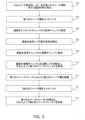
図1は、スペーサ・オン・スペーサ式自己整合4重パターニングと呼ばれるパターニング技術を説明するフローチャートである。図2A-2Eは、図1に示す動作が行われている基板201を例示する。図1の動作を、図2A-図2Eの文脈で説明する。まず、動作101において、基板201を受け取る。基板201は、下地材料202と、コア203と、第1のスペーサ層204とを含む。本明細書で使用される場合、下地材料という文言は、コアの下に配置される材料を指す。図2Aを参照すると、下地材料202は、コア203の下に配置されている。下地材料202は、コア203の形成前に堆積され、様々な材料及び構造を含み得る。様々な例において、下地材料202は、例えば、酸化ケイ素、窒化ケイ素、炭窒化ケイ素、及び/又は炭化ケイ素などの誘電体材料などの、材料の1つ又は複数の層を含む。下地材料202の材料(複数可)は、以下でさらに議論するように、第2のスペーサ層205の材料をマスクとして使用してエッチングできるように選択される。 FIG. 1 is a flow chart illustrating a patterning technique called spacer-on-spacer self-aligned quadruple patterning. FIGS. 2A-2E illustrate a
第1のスペーサ層204は、図2Aに示すように、コア203をコンフォーマルに被覆する。次に、動作103において、第1のスペーサ層204がエッチバックされる。図2Bに示すように、第1のスペーサ層204の材料(第1のスペーサ材料と呼ぶこともある)は、水平配向表面からは除去されるが、垂直配向表面上では実質的に保持される。このエッチング動作は、エッチングを行うように構成された反応チャンバで行われる。次に、動作105において、図2Cに示すように、コア203が除去される。この時点で、第1のスペーサ層204の残存する部分は、分離した別個の垂直配向フィーチャであり、第1のスペーサフィーチャ204’と呼ぶ場合もある。The
動作107において、基板201は、エッチングを行うように構成されたチャンバ内の支持体(しばしば静電チャックと呼ばれる)から取り外され、ウェット洗浄を行うように構成された別のチャンバに移される。次に、動作109において、基板201はウェット洗浄動作に付され、不要な材料が除去される。当業者であれば理解するであろうが、一例では、この不要な材料は、第1のスペーサ層204が動作103でエッチバックされている間に発生し得る。別の例では、コア203を除去するために実行される動作105は、1つ又は複数の洗浄プロセスで除去可能なポリマー残渣などの望ましくない物質をもたらし得る。次に、動作111において、基板201は、洗浄を行うように構成されたチャンバから、堆積を行うように構成されたチャンバに移送される。In
図2Dは、洗浄のために移送され、洗浄され、そして堆積のために移送された後の基板201を例示する。基板201に作用する様々な力によって、図2Dに示すように、第1のスペーサフィーチャ204’は望ましくないほど倒れる/傾く可能性がある。例えば、基板201が移送されるたびに機械的な振動が発生する場合がある。このような機械的振動は、基板のエッチングに使用される基板支持体から基板201を取り外す際に、動作107において特に問題となる場合がある。エッチング装置はしばしば、差動電圧の印加により処理中に基板201を静電チャックに密着固定する静電チャックを使用する。基板201をデチャックする(例えば、静電チャックから解放/除去する)と、基板201は若干ジャンプする。このジャンプにより、基板201に機械的振動が発生し、第1のスペーサフィーチャ204’の倒壊を引き起こし得る。同様に、動作109におけるウェット洗浄プロセスの間及び後に経験される毛管力は、第1のスペーサフィーチャ204’を倒壊させ得る。例えば、ウェット洗浄プロセスからの溶媒が第1のスペーサフィーチャ204’の隣接するペア間で乾燥すると、第1のスペーサフィーチャ204’は互いに向かって引っ張られ、倒れ又は崩壊を引き起こし得る。FIG. 2D illustrates the
動作113において、図2Eに示すように、第2のスペーサ層205が第1のスペーサフィーチャ204’の上に堆積される。第2のスペーサ層205は、コンフォーマルに堆積されるのが望ましい。しかしながら、第1のスペーサフィーチャ204’が倒れたため、第1のスペーサフィーチャ204’の隣接するセット間に空隙206が形成される。この空隙206は好ましくないものであり、故障をもたらし得る。In
図2A-2Eは、スペーサ・オン・スペーサ式SAQP技術中に頻繁に発生する1つの問題を例示する。例示された倒れの問題は、必ずしも基板上のすべての位置で発生するわけではなく、また、本方法を実施するたびに発生するわけでもないことを理解されたい。むしろ、図は、スペーサ・オン・スペーサ式SAQP処理でよく発生する、高い不良率とそれに伴う低収率をもたらす問題を示すことを意図している。Figures 2A-2E illustrate one problem that frequently occurs during spacer-on-spacer SAQP technology. It should be understood that the illustrated collapse problem does not necessarily occur at every location on the substrate, nor does it occur every time the method is performed. Rather, the figures are intended to illustrate a problem that commonly occurs in spacer-on-spacer SAQP processing that results in high defect rates and associated low yields.
図2A-2Eは、スペーサ・オン・スペーサ式SAQP技術において一般的に行われる最後の2つのステップを省略しているが、これらのステップは図1のフローチャートに記載されていることも理解されたい。図1に戻ると、これらのステップは、第2のスペーサ層205をエッチバックして、それによって水平配向表面から除去する一方で、垂直配向表面には実質的にそのまま残すための動作115を含む。このステップは、動作103における第1のスペーサ層204のエッチバックと同様である。次に、動作117において、第1のスペーサ層フィーチャ204’が除去される。このステップは、動作105におけるコア203を除去することと同様である。第1のスペーサフィーチャ204’が除去された後、第2のスペーサ層205の残存する(垂直配向)部分は、互いに分離した別個のものであり、第2のスペーサフィーチャ(図示せず)を形成する。図2A-2Eでは、さらなる処理を成功裏に行えないほど図2Eのフィーチャが既に損なわれているため、これらの最後の2つのステップを省略する。上述したように、下地材料202(又はその上面部分)の材料(複数可)は、第2のスペーサフィーチャをマスク層として使用して下地材料202をエッチングできるように、選択される。いくつかの場合において、下地材料202は、窒化ケイ素、炭化ケイ素、及び/又は炭窒化ケイ素の1つ又は複数の層を含む。いくつかのそのような場合において、第2のスペーサ層205及び第2のスペーサフィーチャは、酸化ケイ素である。いくつかの他の場合において、第2のスペーサ層205及び第2のスペーサフィーチャは、窒化ケイ素である。他の材料の組み合わせが特定の実装において使用されてもよい。It should also be understood that Figures 2A-2E omit the last two steps typically performed in spacer-on-spacer SAQP techniques, but these steps are described in the flow chart of Figure 1. Returning to Figure 1, these steps include
図1及び図2A-2Eに関連して上述した問題点を克服するために、新たなプロセスフローが用いられる。この新たなプロセスフローは、基板が洗浄され、第2のスペーサ層を堆積するためのチャンバに移送された後まで、コアの除去を遅らせる。そのため、コアは、移送や洗浄の間、構造的に支持され、それによってこれらのステップ中に第1のスペーサフィーチャが倒れるリスクを最小化する。コアは、第2のスペーサ層の堆積に使用されるのと同じチャンバで除去されるため、コアの除去は第2のスペーサ堆積の場(inーsitu)で行われると考えられる。この新たなプロセスフローにより、製造不良が大幅に減少するため、従来技術と比較して飛躍的に高い収率を達成する。To overcome the problems discussed above in connection with Figures 1 and 2A-2E, a new process flow is used. The new process flow delays removal of the core until after the substrate has been cleaned and transferred to a chamber for depositing the second spacer layer. Thus, the core is structurally supported during transfer and cleaning, thereby minimizing the risk of the first spacer feature collapsing during these steps. Since the core is removed in the same chamber used to deposit the second spacer layer, core removal is considered to be in-situ during the second spacer deposition. This new process flow achieves a significantly higher yield compared to the prior art, as manufacturing defects are significantly reduced.
図3は、本明細書の様々な実施形態に係るスペーサ・オン・スペーサ式自己整合4重パターニングを実行するためのフローチャートを示す。図4A-4Fは、図3に記載された方法が行われている、部分的に製造された半導体デバイスを例示する。図3の動作について、図4A-4Fを参照して説明する。Figure 3 illustrates a flow chart for performing spacer-on-spacer self-aligned quadruple patterning according to various embodiments herein. Figures 4A-4F illustrate a partially fabricated semiconductor device on which the method described in Figure 3 has been performed. The operation of Figure 3 will be described with reference to Figures 4A-4F.
まず、動作301において、基板401を受け取る。基板401は、下地材料402と、コア403と、第1のスペーサ層404とを含む。第1のスペーサ層404は、図4Aに示すように、コア403をコンフォーマルに被覆する。一般的に、従来の材料がこれらの層の各々に使用されてよい。一実施形態では、コアは、灰化プロセス中に望ましくない残留材料を残すことなく灰化可能な材料で作製され、又はそのような材料を含むことができる。本明細書において定義されるように、灰化プロセスは、熱、又は、酸素含有プラズマ若しくは水素含有プラズマなどのプラズマに曝露することにより、フォトレジストなどの1つ又は複数の有機材料を除去する剥離処理の一種を指す。一例では、コアの材料は、例えば、炭素、シリコン、ゲルマニウム、スズ、鉛などの周期表のIVA族を含むことができ、又はそれらから選択することができる。いくつかの例では、コアの材料は、酸化スズ、酸化鉛、又はそれらの組み合わせを含んでもよい。また、これらの材料の任意の組み合わせを使用してもよい。具体的な一例として、コアは、スピンオン法、化学蒸着法、又はプラズマ励起化学蒸着(PECVD)法により形成された炭素又は炭素系材料である。これら又は他の例において、第1のスペーサ層は、窒化ケイ素、酸化チタン、酸化スズ、酸化ハフニウム、又は酸化ジルコニウムなどの誘電体材料で作られてもよい。他の材料が適宜使用されてもよい。第1のスペーサ層は、原子層堆積又は化学蒸着(いずれも、プラズマエネルギー又は熱エネルギーによって駆動され得る)によって堆積させてもよい。場合によっては、方法は、下地材料402上にコア403を形成するステップと、コアの上に第1のスペーサ層404を堆積するステップとをさらに含んでもよい。First, in
次に、動作303において、第1のスペーサ層404がエッチバックされる。図4Bに示すように、第1のスペーサ層404の材料(第1のスペーサ材料と呼ぶこともある)は、水平配向表面からは除去されるが、垂直配向表面では実質的に保持される。このエッチング動作は、エッチングを行うように構成されたチャンバで行われる。第1のスペーサ層404は、第1のスペーサ層の材料をエッチングするように構成された、エッチング化学作用、プラズマ、及び指向性イオン流出の組み合わせに基板を曝露することによってエッチバックされてもよい。エッチングプロセスは異方性エッチングである。Next, in
次に、動作305において、基板401(例えば、図4Bに示すように、下地材料402の上に配置されているコア403に隣接する第1のスペーサ層404の残存する材料を有する)は、エッチングを行うように構成されたチャンバから、洗浄を行うように構成されたチャンバに移送される。動作307において、基板401は洗浄され、不要な材料(図示せず)が除去される。不要な材料は、典型的には、動作303において第1のスペーサ層をエッチバックした結果、基板401上に存在する材料である。洗浄プロセスは、例えばHFを用いたウェット洗浄プロセスであってもよい。HFは、典型的には少なくとも約10:1(水:HF)、場合によっては約300:1、場合によっては最大約1000:1の割合で、水(例えば脱イオン水)で希釈される。特定の実施形態では、HF溶液は、緩衝溶液であってもよい。これら又は他の場合において、HF溶液は、水酸化アンモニウム及び/又は過酸化水素などの低塩基性試薬を含んでもよい。場合によっては、洗浄プロセスはドライ洗浄プロセスであってもよい。その場合、基板をプラズマに曝露して不要な材料を除去してもよい。Next, in
他の場合において、洗浄プロセスは完全に省略されてもよい。例えば、第1のスペーサ層404の材料及び/又はコア403の材料は、例えば、基板上に再堆積する不揮発性物質の形成なしに、きれいに除去できるように選択されてもよい。このような実施形態では、洗浄動作で除去すべき不要な材料がほとんど又は全くない場合もある。洗浄が省略される実施形態では、洗浄に関連する移送ステップも同様に省略してもよい。例えば、図3を参照すると、動作305、307、及び309は、基板をエッチングチャンバから堆積チャンバに移送することを含む単一の動作に置き換えられてもよい。別の例では、エッチングチャンバと堆積チャンバとは同じ反応チャンバであってもよい。この場合、動作305、307、及び309を完全に省略してもよい。In other cases, the cleaning process may be omitted entirely. For example, the material of the
洗浄工程を省略する利点の1つは、異なるチャンバ及び/又はツール間で基板を移送する回数を減らすことである。これは、基板上の任意のフィーチャが処理/移送中に損なわれるリスクをさらに低減する。エッチングチャンバと堆積チャンバとが同じ反応チャンバ(例えば、反応チャンバは、所望の通り、エッチングと堆積とを行うように構成されている)である一例では、洗浄動作の省略により、動作303(例えば、第1のスペーサ層をエッチバックする)と動作311(コアを除去し、それによって第1のスペーサフィーチャを形成する)との間で基板を移送する必要をなくす。One advantage of omitting the cleaning step is that it reduces the number of times the substrate is transferred between different chambers and/or tools. This further reduces the risk that any features on the substrate are damaged during processing/transfer. In one example where the etch chamber and deposition chamber are the same reaction chamber (e.g., the reaction chamber is configured to etch and deposit as desired), omitting the cleaning operation eliminates the need to transfer the substrate between operation 303 (e.g., etching back the first spacer layer) and operation 311 (removing the core, thereby forming the first spacer feature).
図3の実施形態に戻ると、動作309において、基板401は、洗浄を行うように構成されたチャンバから、堆積を行うように構成されたチャンバへと移送される。これは、第1のスペーサ層を堆積するために使用されたチャンバと同じ又は異なるチャンバであってもよく、さらに、第1のスペーサ層をエッチバックするのに使用されたチャンバと同じ又は異なるチャンバであってもよい。Returning to the embodiment of FIG. 3, in
とりわけ、動作305と307と309とはすべて、図4Bに示すように、コア403が依然として基板401上に存在する間に行われる。このようにして、コア403は、第1のスペーサ層404/第1のスペーサフィーチャ404’への機械的支持を提供し、移送と洗浄動作中にそれらの望ましからざる倒れを防止する。基板が、第2のスペーサ層が堆積される(以下でさらに議論する)堆積チャンバに移送されると、図4Cに示すように、動作311においてコア403が除去される。コアは、灰化などの乾燥プロセスによって除去されてもよい。この時点で、第1のスペーサ層404の残存する部分は、第1のスペーサフィーチャ404’と呼ばれることもある、分離した別個の異なる垂直配向フィーチャである。コア403は、コアの材料を除去するように構成されたプラズマに基板を曝露することによって除去されてもよい。上述したように、一例では、コア403は、炭素又は炭素系材料であり、基板を酸素含有プラズマに曝露することによって除去できる。反応物の例として、O2及び他の酸素含有種が挙げられる。いくつかの他の例では、コア403は、1つ又は複数の金属酸化物材料(例えば、酸化スズ、酸化鉛など)を含んでもよく、基板を水素含有プラズマに曝露することによって除去できる。使用され得る反応物の例として、H2、NH3、CH4、及び他の水素含有種が挙げられる。特定の例では、プラズマは、H2とN2との混合物を含む。プラズマの酸化及び還元を、特定のコア材料を除去するために適宜使用してもよい。 Notably,
次に、動作313において、図4Dに示すように、第2のスペーサ層405が、第1のスペーサフィーチャ404’の上に堆積される。第2のスペーサ層405は、原子層堆積又は化学蒸着(いずれも、プラズマエネルギー又は熱エネルギーによって駆動され得る)により堆積されてもよい。第2のスペーサ層405は、酸化ケイ素、窒化ケイ素、酸化チタン、酸化スズ、酸化ジルコニウム、酸化ハフニウムなどの誘電体材料であってもよい。一般に、第1のスペーサ層404の材料は、第2のスペーサ層405の材料とは異なる組成を有するべきである。様々な材料の組み合わせを、第1のスペーサ層404及び第2のスペーサ層405に使用できる。Next, in
一例では、コア403は炭素又は炭素系材料であり、第1のスペーサ層404は酸化スズ又は酸化チタンであり、第2のスペーサ層405は酸化ケイ素又は窒化ケイ素である。別の例では、コア403は炭素又は炭素系材料であり、第1のスペーサ層404は酸化ケイ素又は窒化ケイ素であり、第2のスペーサ層405は酸化スズ、酸化チタン、又は酸化鉛である。別の例では、コア403は、酸化スズ、酸化鉛、又はそれらの組み合わせであり、第1のスペーサ層404は酸化チタンであり、第2のスペーサ層405は任意の酸化物(例えば、酸化ケイ素、金属酸化物など)又は窒化ケイ素である。In one example, the
図3に記載のプロセスフローは、図1及び2Dに関連して説明されたように第1のスペーサフィーチャ404’が倒れることなく、垂直のままであることを保証する。このように、第2のスペーサ層405は、図2Eに関連して説明した空隙又は他の望ましくない欠陥の形成なしに、第1のスペーサフィーチャ404’上にコンフォーマルに堆積する。The process flow described in FIG. 3 ensures that the first spacer features 404' remain vertical, rather than toppling, as described in connection with FIGS. 1 and 2D. In this manner, the
次に、動作315において、図4Eに示すように、第2のスペーサ層405がエッチバックされる。エッチバック動作は、第2のスペーサ層405を水平表面から除去するが、垂直表面上では実質的に保持する。第2のスペーサ層405は、第2のスペーサ層の材料をエッチングするように構成された、エッチング化学作用、プラズマ、及び指向性イオン流出の組み合わせに基板を曝露することによってエッチバックされてもよい。エッチングプロセスは、異方性エッチングプロセスである。Next, in
動作317において、図4Fに示すように、第1のスペーサフィーチャ404’が除去される。この時点で、第2のスペーサ層405の残存する部分は、互いに分離した別個のものであり、第2のスペーサフィーチャ405’を形成している。第1のスペーサフィーチャ404’は、低バイアス(例えば、≦10V)の等方性選択的エッチングにおける灰化/掘り起こしによって除去されてもよい。第1のスペーサフィーチャ404’は、基板401の下地材料402又は第2のスペーサフィーチャ405’を著しくエッチングすることなく、選択的に除去される。In
上述したように、コアは、炭素若しくは炭素含有材料、又は金属酸化物材料であってもよい。様々な実施形態において、コアは、特定の材料特性を有してもよい。例えば、コアの材料は、比較的低い応力(例えば、約50MPa以下の絶対値を有する堆積後ブランケット応力を有する)及び高いヤング率(例えば、30GPaより高い)を示す場合がある。特定の実施形態では、コアの材料は、例えば、酸素含有プラズマ又は水素含有プラズマなどのプラズマに曝露された場合に、灰化可能である場合がある。灰化反応は、少なくとも1つの固相反応物質から揮発性生成物を生成するが、基板上に再堆積し得るポリマー又は他の不揮発性物質はほとんど生成されない。炭素又は炭素含有コアの場合、炭素を酸素含有プラズマと反応させて揮発性二酸化炭素を形成してもよい。金属酸化物ベースのコアの場合、水素含有プラズマを用いて金属酸化物を除去してもよい。As discussed above, the core may be a carbon or carbon-containing material, or a metal oxide material. In various embodiments, the core may have certain material properties. For example, the core material may exhibit relatively low stress (e.g., a post-deposition blanket stress having an absolute value of about 50 MPa or less) and a high Young's modulus (e.g., greater than 30 GPa). In certain embodiments, the core material may be ashed when exposed to a plasma, such as, for example, an oxygen-containing plasma or a hydrogen-containing plasma. The ashing reaction produces volatile products from at least one solid-phase reactant, but little polymer or other non-volatile material that may be redeposited on the substrate. In the case of a carbon or carbon-containing core, the carbon may be reacted with an oxygen-containing plasma to form volatile carbon dioxide. In the case of a metal oxide-based core, a hydrogen-containing plasma may be used to remove the metal oxide.
図4A-4Fに示すように、開示されたプロセスフローは、基板表面に存在するフィーチャの数を4倍にするために使用され得る。このプロセスは、一般に、スペーサ・オン・スペーサ(SoS)式自己整合4重パターニング(SAQP)と呼ばれる。図3に記載された特定のプロセスフローは、第2のスペーサ堆積の場でのコア引き抜き(CoPS:Core Pull In-Situ to Second Spacer Deposition)と呼ばれることもある。この名称は、コアが第2のスペーサ堆積の場(inーsitu)で(例えば、同じチャンバで)除去されるという事実に由来する。CoPSのプロセスフローにより、製造上の欠陥が大幅に減少するため、機能しない基板/デバイスの数を最小限に抑え、廃棄物を削減し、効率を高めることができる。その結果、製造コストが削減される。As shown in Figures 4A-4F, the disclosed process flow can be used to quadruple the number of features present on a substrate surface. This process is commonly referred to as Spacer-on-Spacer (SoS) Self-Aligned Quadruple Patterning (SAQP). The particular process flow described in Figure 3 is sometimes referred to as Core Pull In-Situ to Second Spacer Deposition (CoPS). The name comes from the fact that the core is removed in-situ (e.g., in the same chamber) during the second spacer deposition. The CoPS process flow significantly reduces manufacturing defects, thereby minimizing the number of non-functional substrates/devices, reducing waste, and increasing efficiency, resulting in reduced manufacturing costs.
図3及び図4A-4Fでは、多数の異なるステップが示されているが、様々な実施形態において特定の動作を省略してもよいことを理解されたい。同様に、いくつかの実施形態において追加のステップが行われてもよい。図3を参照すると、一実施形態は、動作311だけを含む。別の実施形態は、動作311及び313を含む。別の実施形態は、動作311、313、及び315を含む。別の実施形態は、動作311、313、315、及び317を含む。これらの実施形態のいずれもが、動作301、303、305、及び307のうちの任意の1つ又は複数を含むように変更可能である。While many different steps are shown in Figures 3 and 4A-4F, it should be understood that certain operations may be omitted in various embodiments. Likewise, additional steps may be performed in some embodiments. With reference to Figure 3, one embodiment includes
図3及び図4A-4Fに記載されたプロセスフローは、メモリデバイスの製造のように、フィーチャの数が4倍であることが望まれる文脈において、うまく機能する。他のいくつかのデバイス(例えば、論理デバイス)は、より複雑な構造を有する場合があり、そのような場合、フィーチャの数を4倍未満に増やすことが望ましいこともある。そのような場合、特定のフィーチャ(例えば、第1のスペーサフィーチャ)は、パターンを2倍にするために使用される前に除去の対象とされてもよい。図5は、このような実施形態を説明するフローチャートであり、カットマスク統合スキームと呼ばれることもある。図5の方法は、図5の動作が行われている部分的に製造された半導体デバイスを示す図6A-6Iの文脈で説明される。概して、図5の動作の多くは、図3の動作に類似しており、図3に関連して提供される詳細は、図5の方法にも適用される。簡潔さのために、多くのそのような詳細は、図5の説明から省略される。The process flow described in Figures 3 and 4A-4F works well in contexts where a quadruple in the number of features is desired, such as in the fabrication of memory devices. Some other devices (e.g., logic devices) may have more complex structures, and in such cases it may be desirable to increase the number of features by less than four times. In such cases, certain features (e.g., the first spacer feature) may be targeted for removal before being used to double the pattern. Figure 5 is a flow chart illustrating such an embodiment, sometimes referred to as a cut mask integration scheme. The method of Figure 5 is described in the context of Figures 6A-6I, which show a partially fabricated semiconductor device on which the operations of Figure 5 have been performed. In general, many of the operations of Figure 5 are similar to those of Figure 3, and the details provided in connection with Figure 3 also apply to the method of Figure 5. For the sake of brevity, many such details are omitted from the description of Figure 5.
図5の方法は、基板601を受け取る動作501で始まる。基板601は、図6Aに示すように、下地層602と、コア603と、第1のスペーサ層604とを含む。コア603及び第1のスペーサ層604の堆積、並びに第1のスペーサ層604のエッチバック(動作303に類似)に関連するステップは、図からは省略されているが、これらのステップは特定の実施形態に含まれる場合もある。特定の基板移送ステップも図から省略されているが、基板は、各ステップごとに必要に応じて異なるツールに移送されることが理解される。方法は、動作502へと続き、ここで、基板は洗浄に付され、不要な材料が除去される。この不要な材料は、第1のスペーサ層604のエッチバック中に頻繁に発生する。図3を参照して説明したように、洗浄動作502は、特定の実施形態では省略されてもよい。5 begins with
方法は動作503へと続き、図6Bに示すように、平坦化層607、中間層608、及びパターニングされたフォトレジストの層609が、基板601上に順次設けられる。多くの場合、平坦化層607は、スピンオンカーボン又はスピンオンガラスであり、これらは自己平坦化する。あるいは、平坦化層607は、化学蒸着又は他の方法により堆積されてもよい。平坦化層607の上面/部分は、典型的に平らである。平坦化層607は、マスク又はブロックマスクとも呼ばれる場合がある。様々に異なる従来材料が中間層608に使用されてもよく、中間層608は、スピンオン技術、PECVD技術などによって堆積されてもよい。フォトレジスト609は、任意の種類のフォトレジストであってよい。特定の実施形態では、フォトレジスト609は、極端紫外線(EUV)フォトレジストである。このようなEUVフォトレジストは、現在使用及び開発されている標準的な13.5nmのEUV波長を用いて露光されてもよい。しかしながら、一般に248nm又は193nmのエキシマレーザ源の使用を意味するDUV(深紫外線)、X線範囲のより低いエネルギー範囲におけるEUVを正式に含むX線、及び広いエネルギー範囲をカバーできる電子ビームを含む、他の放射線源が、場合によっては使用されてもよい。The method continues with
フォトレジストは、動作503の一部として、開口部610を含むように堆積され、次いでパターニングされる。この例では、開口部610は、左から数えて残存する第1のスペーサ層604の第3の部分の上方に配置される。他の実施形態では、開口部610は他の位置にあってもよい。この位置決めにより、開口部610は、以下でさらに説明するように、残存する第1のスペーサ層604の第3の部分を除去するために使用され、それにより、この位置での第1のスペーサフィーチャ604’の形成を防ぐ。As part of
特に、動作502及び503は、コア603が基板601上に依然として存在する間に行われる。これにより、コア603が、移送及び洗浄動作中に、第1のスペーサ層604の残存する部分に機械的支持を与えることが保証される。より従来のプロセスフローでは、コア603は、第1のスペーサ層604がエッチバックされた直後(例えば、動作501の後)、基板が洗浄される前(例えば、動作502の前)に除去されることになる(それによって第1のスペーサフィーチャ604’を形成する)。洗浄後、平坦化層607は、コア603が除去された位置に追加的に堆積される。従来のプロセスフローの結果として、第1のスペーサフィーチャ604’は、様々な移送及び洗浄動作中に機械的支持を欠き、図2Dに関連して説明したように、倒壊に対して脆弱なままであろう。代わりに、基板の移送、洗浄、並びに、平坦化層607、中間層608、及びフォトレジスト609の堆積を通してコア603を維持することによって、図5のプロセスフローは、第1のスペーサ層604の残存する部分が様々な処理ステップを通して適切に支持され、それらが倒れてさらなる処理問題を引き起こすのを防ぐことを保証する。In particular,
図5の方法は、動作505へと続き、図6Cに示すように、中間層608は、開口部610の位置でエッチングされる。フォトレジスト609はマスクとして機能し、中間層608の残存する部分を保護する。しかしながら、フォトレジスト609は、中間層608が動作505においてエッチングされる際に、部分的に又は完全に除去されてもよい。エッチング動作は、開口部610において中間層の材料を除去するように構成された化学作用及び/又はプラズマに基板を曝露することを含んでもよい。エッチングプロセスは、フォトレジスト609などの他の材料よりも大きな程度に中間層608の材料をエッチングするという点で選択的であってもよい。5 continues with
次に、方法は動作507へと続き、図6Dに示すように、平坦化層607が開口部610の位置でエッチングされる。中間層608は(残存するフォトレジスト609と同様に)平坦化層607がエッチングされている間、マスクとして機能する。このように、中間層608は、マスク又はマスク層とも呼ばれることがある。平坦化層607は、平坦化層607を除去するように構成された化学作用及び/又はプラズマに基板を曝露することによって、開口部610において除去されてもよい。エッチングプロセスは、中間層608などの他の材料よりも大きな程度に平坦化層607をエッチングするという点で選択的であってもよい。一例では、基板は、開口部610において平坦化層607を除去するために、酸素含有プラズマに曝露される。中間層608の一部は、動作507の間に除去されてもよい。この時点で、平坦化層607の上面部分は、実質的に平らである(例えば、開口部610を除いて平らである)。The method then continues with
次に、動作509において、図6Eに示すように、残存する第1のスペーサ層604の一部が開口部610の位置で除去される。中間層608は、この動作の間、マスクとして機能し、かつこのステップの間、全体的に又は部分的に除去されてもよい。様々な実施形態において、中間層608は、動作509の間に完全に除去される。そのような場合、残存する平坦化層607は、開口部610以外の位置で基板601上の様々なフィーチャ/構造体を保護するためにマスクとして機能してもよい。エッチングプロセスは、中間層608及び/又は平坦化層607などの他の材料よりも大きな程度に第1のスペーサ層604の材料を除去するように構成された化学作用及び/又はプラズマに基板を曝露することを含んでもよい。Next, in
この時点で、開口部610の位置に対応する第1のスペーサ層604の部分は完全に除去される。そのため、第1のスペーサ層604は、この位置で第1のスペーサフィーチャ604’を形成することはない。開口部610において第1のスペーサ層604を除去するために、基板は、第1のスペーサ層604の材料を除去するように構成された化学作用及び/又はプラズマに曝露されてもよい。言い換えれば、エッチングプロセスは選択的である。At this point, the portion of the
方法は動作511に続き、図6Fに示すように、コア603及び残存する平坦化層607が除去される。このとき、第1のスペーサ層604の残存する部分は、互いに分離した別個のものであり、第1のスペーサフィーチャ604’と呼ばれることもある。典型的には、コア603及び平坦化層607は、灰化などの乾燥プロセスを通じて除去される。一実施形態では、コア603及び平坦化層607は、単一のステップで一緒に除去される。別の実施形態では、コア603は、平坦化層607が除去された後に除去されてもよい。従来のプロセスフローでは、コア603は、この時点までに既に平坦化層607によって置き換えられており、そのため、単一の灰化ステップのみが使用される。The method continues with
この時点で、図6Fの基板601は、図4Cの基板501に類似している。すなわち、基板601は、下地材料602と第1のスペーサフィーチャ604’とを含む。方法は、図3及び図4D-4Fで説明したものに類似するステップへと続く。動作513において、図6Gに示すように、第2のスペーサ層605が第1のスペーサフィーチャ604’の上に堆積される。動作515において、図6Hに示すように、第2のスペーサ層605がエッチバックされる。動作517において、図6Iに示すように、第1のスペーサフィーチャ604’が除去される。このとき、第2のスペーサ層605の残存する部分は、互いに分離した別個のものであり、第2のスペーサフィーチャ605’と呼ばれることもある。At this point, the
図6A-6Iに示すように、図5で説明したプロセスフローは、基板601上に存在するフィーチャの数を3倍にした(例えば、基板は2つのフィーチャで始まり、6つのフィーチャで終了した)。もちろん、図5の方法を実施する際に、特定の用途のために所望されるようにフィーチャ(例えば、第1のスペーサフィーチャ)を除去の対象とし、任意の数の開口部610を使用できる。一般に、図5の方法は、フォトレジスト609に設けられた開口部610の数に応じて、基板上のフィーチャの数を3:1から4:1の倍率で増加させるために使用されてもよい。結果として得られたフィーチャのレイアウトは、開口部610の位置決めに基づいて制御できる。As shown in Figures 6A-6I, the process flow described in Figure 5 tripled the number of features present on the substrate 601 (e.g., the substrate started with two features and ended with six features). Of course, in performing the method of Figure 5, features (e.g., the first spacer feature) can be targeted for removal and any number of
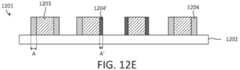
図13は、半導体基板を処理する方法を説明するフローチャートを示し、基板は、不均一な限界寸法を有するフィーチャを含むようにパターニングされる。図3及び図5で説明した方法と同様に、図13の方法は、いくつかの処理ステップを通してコアが基板上に維持されることを保証し、コアが隣接する構造体に機械的支持を与えることを可能にし、それによって、そのような構造体が崩壊することを防ぐ。図12A-12Hは、図13の方法が行われている部分的に製造された半導体基板を示す。これらの図は、明確化のために、一緒に説明される。Figure 13 shows a flow chart illustrating a method of processing a semiconductor substrate, where the substrate is patterned to include features having non-uniform critical dimensions. Similar to the methods described in Figures 3 and 5, the method of Figure 13 ensures that the core remains on the substrate through several processing steps and allows the core to provide mechanical support to adjacent structures, thereby preventing such structures from collapsing. Figures 12A-12H show a partially fabricated semiconductor substrate on which the method of Figure 13 has been performed. These figures are described together for clarity.
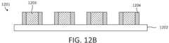
図13の方法は、動作1301で始まり、ここで基板1201を反応チャンバで受け取る。基板1201は、例えば、基板支持体上に配置されてもよい。基板1201は、図12Aに示すように、下地材料1202と、コア1203と、第1のスペーサ層1204とを含む。次に、動作1303において、図12Bに示すように、第1のスペーサ層1204がエッチバックされる。この動作は、例えば、図3の動作303における第1のスペーサ層のエッチバックに類似する。動作1305において、基板は洗浄に付され、例えば動作1303における第1のスペーサ層のエッチバック中に発生し得る不要な材料を除去する。次に、動作1307において、図12Cに示すように、平坦化層1205が堆積され、パターニングされる。平坦化層1205は、図6B-6Eの平坦化層607に類似しており、同様の技術によりパターニングされてもよい(例えば、1つ又は複数の追加の層を、リソグラフィと組み合わせて使用してもよい)。The method of FIG. 13 begins with
平坦化層1205は、図12Cに示すように、下層構造の特定の部分を露出させるようにパターニングされる。特に、平坦化層1205は、基板上に露出領域(例えば、平坦化層1205が除去された領域)及び保護領域(例えば、平坦化層が残っている領域)を画定するようにパターニングされる。以下でさらに説明するように、これによって、不均一な限界寸法を有するフィーチャを形成できる。The
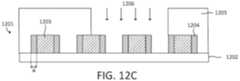
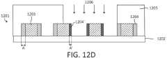
動作1309において、第1のスペーサ層1204の露出部分が、露出領域内の第1のスペーサ層1204の厚さを減らすために、イオン、化学物質、及び/又はプラズマ1206への曝露を通してトリミングされる。図12Cは、このトリミング動作1309の開始時の基板1201を示し、図12Dは、このトリミング動作1309の終了時の基板1201を示す。トリミングの前に、第1のスペーサ層1204は、第1のスペーサ層1204が残っている全ての領域において厚さAを有する。厚さは、基板表面に平行な方向で測定される。トリミング後、第1のスペーサ層1204は、保護領域において厚さAを有し、露出領域においてより小さい厚さA’を有する。この時点で、これらの狭められたフィーチャは、トリミングされた第1のスペーサ1204’と呼ばれることもある。図12D-12Hは、3つの隣接するトリミングされた第1のスペーサ1204’を示すが、任意の数のトリミングされた第1のスペーサ1204’を使用してもよく、かつ特定の用途に対して任意の所望のレイアウトで形成してもよいことが理解される。In
次に、動作1311において、図12Eに示すように、平坦化層1205が除去される。このステップは、図5の動作511における平坦化層の除去に類似している。動作1313において、図12Fに示すように、コア1203が除去される。このステップは、図5の動作511におけるコアの除去に類似している。場合によっては、平坦化層1205及びコア1203は、別々のステップで除去されてもよく、他の場合には、これらは単一のステップで一緒に除去されてもよい。コア1203が除去された後、第1のスペーサ層1204の残存するトリミングされていない部分から形成されたフィーチャ、及びトリミングされた第1のスペーサ1204’から形成されたフィーチャは、互いに分離した別個のものであり、第1のスペーサフィーチャと呼ばれることもある。Next, in
図12Fは、第1のスペーサフィーチャの不均一な限界寸法を明確に示す。特に、トリミングを受けない第1のスペーサ層1204から形成された第1のスペーサフィーチャ(明るい灰色で示される)は厚さAを有するが、トリミングされた第1のスペーサ1204’から形成された第1のスペーサフィーチャ(暗い灰色で示される)はより狭い厚さA’を有する。Figure 12F clearly shows the non-uniform critical dimensions of the first spacer features. In particular, the first spacer feature formed from the untrimmed first spacer layer 1204 (shown in light gray) has a thickness A, while the first spacer feature formed from the trimmed first spacer layer 1204' (shown in dark gray) has a narrower thickness A'.
動作1315において、図12Gに示すように、第2のスペーサ層1207が堆積される。第2のスペーサ層1207は、厚さBを有する。この堆積は、図3の動作313及び図5の動作513における第2のスペーサ層の堆積に類似している。次に、動作1317において、図12Hに示すように、第2のスペーサ層1207は、エッチバックされる。このエッチバックは、図3の動作315及び図5の動作515に類似している。図12Hに示される基板1201は、その上に、異なる限界寸法を有する2つの異なる種類のフィーチャを有する。ある種類のフィーチャは、厚さA+2Bを有し、動作1309におけるトリミング中に下層構造を保護するために平坦化層1205が存在した領域に形成されている。他の種類のフィーチャは、より狭く、厚さA’+2Bを有し、平坦化層1205が除去されて下層構造が露出した領域に形成され、ここで第1のスペーサ層1204の一部がトリミングされて、トリミングされた第1のスペーサ1204’が形成される。In
特定の実施形態では、動作1315及び1317は省略されてもよい。第2のスペーサ層1207の堆積がなくても、例えば図12Fに示すように、異なる限界寸法を有するフィーチャを形成できる。いくつかの実施形態では、追加の動作が行われてもよい。一例として、第1のスペーサ層1204及びトリミングされた第1のスペーサ1204’からの材料は、動作1317の後に除去されてもよい。これは、均一な厚さBを有するが、隣接するフィーチャのセット間の間隔が異なるフィーチャを生成するであろう。例えば、隣接するフィーチャのいくつかのセットは距離Aだけ分離され、他方で隣接するフィーチャの他のセットは距離A’だけ分離されることになる。In certain embodiments,
図13及び図12A-12Hに示される方法に関する1つの注目すべき特徴は、動作1303における第1のスペーサ層1204のエッチバック、動作1305における基板1201の洗浄、動作1307における平坦化層1205の堆積及びパターニング、並びに動作1309におけるトリミングされた第1のスペーサ1204’を形成するための第1のスペーサ層1204の露出部分のトリミングを含むいくつかの処理ステップを通して、コア1203が基板1201に留まっている点である。さらに、図13で概説した処理ステップの多くは、第2のスペーサ層1207を堆積するために使用される反応チャンバで行われてもよい。例えば、少なくとも、動作1309で第1のスペーサ層1204をトリミングするステップ、動作1311で平坦化層1205を除去するステップ、動作1313でコア1203を除去するステップ、及び動作1315で第2のスペーサ層1207を堆積するステップは、全てこの反応チャンバで行われてもよい。基板1201が第2のスペーサ層1207を堆積するために使用される反応チャンバに移送された後まで、コア1203が基板1201上に確実に留まるようにすることによって、フィーチャ崩壊のリスクは実質的に低減又は排除される。関連するフィーチャが適切な支持を欠いている間は、基板を、移送、洗浄、又は崩壊を引き起こす可能性のある他の動作に付さないため、このリスクは低減される。13 and 12A-12H is that the
様々な種類のフィードバックが、本明細書の実施形態を実施する際に使用されてもよい。例えば、コアを除去するときに(例えば、動作311、511、又は1313において)、フィードバックを使用して、コア材料が基板から十分に除去される時間を判定してもよい。これにかかる時間は、様々な要因に基づいて、日ごとに、又は基板ごとに変化し得る。コア除去プロセスの監視に使用され得るフィードバック方法の例として、発光分光分析(OES)及びレーザ干渉法(LSR)が挙げられる。リアルタイムフィードバックは、コアが十分に除去された直後にコア除去プロセスを停止でき、したがって、基板上、特に第1のスペーサフィーチャ上の過剰なプラズマ曝露(及び/又は他の厳しい処理条件)を最小限に抑えることができるので、この文脈で有用である。多くの実施形態において、コア除去プロセスは、基板をプラズマ(例えば、酸素含有プラズマ)、時には灰化プラズマとも呼ばれるものに曝露することを含む。コア除去プロセスは、単にプラズマを消すことによって停止されてもよい。コア除去プロセスは、コア除去プロセスが完了又は実質的に完了したことを示すOES及び/又はLSR装置からのフィードバックに応答して停止されてもよい。Various types of feedback may be used in implementing embodiments herein. For example, when removing the core (e.g., in
この文脈において、発光分光分析は、コアを除去するために基板に曝露されるプラズマの光学発光を監視することを含む。コアがプラズマと反応すると、コア材料は反応して消滅し、気相生成物を生成し、気相生成物は真空接続を介してチャンバから除去される。光学発光スペクトルを監視して、気相生成物の存在と相対濃度を検出する。気相生成物は典型的に、除去プロセスの初期に濃度(及び特定の波長における測定線強度)が増加し、その後定常状態に達し、次いで除去プロセスが完了に近づくと減少する。特定の気相生成物の測定強度がある閾値レベルまで下がると、コア材料が除去されたことを意味し、プラズマへの基板のさらなる曝露は不要である(かつ有害な可能性もある)。一例では、コアは炭素又は炭素系材料であり、コアを除去することは、炭素を灰化して気相の二酸化炭素を形成することを含む。プラズマの光学発光スペクトルは、二酸化炭素が放射する波長で監視される。最初は、コアの炭素が反応して消滅し、二酸化炭素が生成されると、二酸化炭素の信号が上昇する。二酸化炭素信号は定常状態に達し、この時点では、チャンバから排出されるのと同じ速度で二酸化炭素が生成されている。最終的に、二酸化炭素信号は0に向かって減少し始め、二酸化炭素が生成されるよりも速くチャンバから除去されていることを示し、除去プロセスが完了した又は完了に近づいていることを意味する。同様の技術は、他の種類のコア材料や灰化プラズマと共に使用されてもよい。In this context, optical emission spectroscopy involves monitoring the optical emission of the plasma that is exposed to the substrate to remove the core. As the core reacts with the plasma, the core material reacts and disappears, producing gas-phase products that are removed from the chamber via a vacuum connection. The optical emission spectrum is monitored to detect the presence and relative concentration of the gas-phase products. The gas-phase products typically increase in concentration (and measured line intensity at a particular wavelength) early in the removal process, then reach a steady state, and then decrease as the removal process approaches completion. When the measured intensity of a particular gas-phase product falls to a certain threshold level, it means that the core material has been removed, and further exposure of the substrate to the plasma is unnecessary (and potentially harmful). In one example, the core is a carbon or carbon-based material, and removing the core involves ashing the carbon to form gas-phase carbon dioxide. The optical emission spectrum of the plasma is monitored at wavelengths at which carbon dioxide emits. Initially, the carbon dioxide signal rises as the carbon in the core reacts and disappears, producing carbon dioxide. The carbon dioxide signal reaches a steady state, at which point carbon dioxide is being produced at the same rate that it is being evacuated from the chamber. Eventually, the carbon dioxide signal will begin to decrease toward zero, indicating that carbon dioxide is being removed from the chamber faster than it is being produced, meaning the removal process is complete or nearing completion. Similar techniques may be used with other types of core materials and ashing plasmas.
上述したように、コア除去プロセスのエンドポイントを検出するために使用され得る別の種類のフィードバックは、レーザ干渉法を含む。この文脈では、レーザ干渉法は、1つ又は複数のレーザを基板上に照射し(単一レーザを使用する場合は、レーザを2つ以上のビームに分割する)、ビームを基板に跳ね返し、基板から戻ってくる干渉パターンを監視することを含む。この技術により、ウェハ表面上での光子と物質の相互作用を調べ、コア除去プロセスがいつ完了したかを検出できる。As mentioned above, another type of feedback that can be used to detect the endpoint of the core removal process involves laser interferometry. In this context, laser interferometry involves shining one or more lasers onto the substrate (if a single laser is used, the laser is split into two or more beams), bouncing the beams off the substrate, and monitoring the interference pattern returning from the substrate. This technique allows one to examine the interaction of photons with matter on the wafer surface and detect when the core removal process is complete.
本明細書の実施形態のいずれかで使用され得る別の種類のフィードバックは、しばしばスキャッタロメトリと呼ばれるOCD(Optical Critical Dimension)計測に関連する。この種類のフィードバックは、コアが除去された後の第1のスペーサフィーチャの幅(例えば、図4C又は図6Fにおける左から右への幅)を測定するために使用されてもよい。様々な実施形態において、コアを除去し、かつ第2のスペーサ層を堆積するために使用されるチャンバは、OCDを実行するためのスキャッタロメトリハードウェアを含んでもよい。このようにして、第1のスペーサフィーチャの幅は、計測のために基板を別のチャンバに移送することなく、堆積チャンバ内でinーsitu測定することができる。そのような基板移送は、例えば図2Dに関連して説明したように、望ましくないことに、第1のスペーサフィーチャの倒れを引き起こす可能性がある。代わりに、基板をデチャックすることなく、又は他の方法で乱すことなく、コアの除去と、第1のスペーサフィーチャの幅の測定と、その後の第2のスペーサ層の堆積のすべてを行うことができる。スキャッタロメトリハードウェアによって測定された幅は、第1のスペーサ層の堆積などの上流プロセスを制御するためのフィードバックとして使用されてもよい。スキャッタロメトリが、第1のスペーサフィーチャが所望よりも狭いことを示す場合、将来処理される基板上により厚い第1のスペーサ層を形成するために、第1のスペーサフィーチャを形成するためのプロセスの持続時間を長くしてもよい。同様に、スキャッタロメトリが第1のスペーサフィーチャが所望よりも広いことを示す場合、将来処理される基板上により狭い第1のスペーサ層を形成するために、第1のスペーサフィーチャを形成するためのプロセスの持続時間を短くしてもよい。代替的に又は持続時間の変更に加えて、第1のスペーサ層の堆積はまた、望ましい場合には、異なるプラズマ条件を使用するようにスキャッタロメトリ結果に基づいて変更されてもよい。これらの変更は、自動プロセス制御に基づいて行われてもよく、又は手動で行われてもよい。Another type of feedback that may be used in any of the embodiments herein relates to OCD (Optical Critical Dimension) metrology, often referred to as scatterometry. This type of feedback may be used to measure the width of the first spacer feature after the core has been removed (e.g., the width from left to right in FIG. 4C or FIG. 6F). In various embodiments, the chamber used to remove the core and deposit the second spacer layer may include scatterometry hardware to perform OCD. In this way, the width of the first spacer feature may be measured in-situ in the deposition chamber without transferring the substrate to another chamber for metrology. Such substrate transfer may undesirably cause the first spacer feature to tip, for example, as described in connection with FIG. 2D. Instead, the core removal, measurement of the width of the first spacer feature, and subsequent deposition of the second spacer layer may all be performed without dechucking or otherwise disturbing the substrate. The width measured by the scatterometry hardware may be used as feedback to control upstream processes, such as the deposition of the first spacer layer. If the scatterometry indicates that the first spacer feature is narrower than desired, the duration of the process for forming the first spacer feature may be increased to form a thicker first spacer layer on future processed substrates. Similarly, if the scatterometry indicates that the first spacer feature is wider than desired, the duration of the process for forming the first spacer feature may be decreased to form a narrower first spacer layer on future processed substrates. Alternatively or in addition to changing the duration, the deposition of the first spacer layer may also be changed based on the scatterometry results to use different plasma conditions, if desired. These changes may be made based on automatic process control or may be made manually.
本明細書に記載されたフィードバックを得るために、第2のスペーサ層を堆積するために使用される堆積チャンバは、関連するフィードバックハードウェアを含むように変更されてもよい。例えば、堆積チャンバは、発光分光分析ハードウェア、レーザ干渉ハードウェア、及び/又は光CD計測/スキャッタロメトリハードウェアを含むように変更されてもよい。第2のスペーサ層を堆積するために使用される従来の堆積チャンバは、そのようなフィードバックハードウェアを含まない。しばしば、第2のスペーサ層は、原子層堆積(これは、プラズマエネルギー及び/又は熱エネルギーによって駆動され得る)により堆積され、これは、非常にゆっくりと予測可能に堆積される。原子層堆積反応の予測可能かつ制御可能な性質のため、堆積プロセスを能動的に監視する必要はない。むしろ、堆積反応のエンドポイントは、堆積速度と所望の膜厚のみに基づいて、確実に予測できる。そのため、第2のスペーサ層を堆積するための従来のチャンバは、エンドポイント検出のためのハードウェアを含まない。同じことが、予測可能な堆積速度を有する他の種類の堆積チャンバ(例えば、化学蒸着チャンバなど)にも当てはまる。同様に、第2のスペーサ層を堆積するための従来のチャンバは、スキャッタロメトリハードウェアを含まない。そのようなハードウェアは、プロセスフローのより早い段階で他のツールで使用されてもよい。しかしながら、第2のスペーサ層を堆積するために使用される堆積チャンバにそのようなハードウェアを含める説得力のある理由は、これまで存在しなかった。To obtain the feedback described herein, the deposition chamber used to deposit the second spacer layer may be modified to include associated feedback hardware. For example, the deposition chamber may be modified to include optical emission spectroscopy hardware, laser interferometry hardware, and/or optical CD metrology/scatterometry hardware. Conventional deposition chambers used to deposit the second spacer layer do not include such feedback hardware. Often, the second spacer layer is deposited by atomic layer deposition (which may be driven by plasma energy and/or thermal energy), which deposits very slowly and predictably. Due to the predictable and controllable nature of the atomic layer deposition reaction, there is no need to actively monitor the deposition process. Rather, the endpoint of the deposition reaction can be reliably predicted based only on the deposition rate and the desired film thickness. As such, conventional chambers for depositing the second spacer layer do not include hardware for endpoint detection. The same is true for other types of deposition chambers (e.g., chemical vapor deposition chambers, etc.) that have predictable deposition rates. Similarly, conventional chambers for depositing the second spacer layer do not include scatterometry hardware. Such hardware may be used in other tools earlier in the process flow; however, there has heretofore been no compelling reason to include such hardware in the deposition chamber used to deposit the second spacer layer.
装置
図7は、様々な実施形態に係る、基板を処理するために使用され得るプロセスステーション700の一実施形態を概略的に示す。例えば、プロセスステーション700は、コアの除去(例えば、動作311、511、及び1313)、追加の平坦化層の除去(例えば、動作511及び1311)、第2のスペーサ層の堆積(例えば、動作313、513、及び1315)、並びにこれらのプロセスに関連する任意の計測及びフィードバック技術の実行を含む、本明細書に記載される多くの動作の実行に使用されてもよい。図3、5、及び/又は13に記載されたプロセスフローを用いて、同じプロセスステーション700でこれらの動作を行うことによって、上述した利点が達成され得る。例えば、コア(及び存在する場合は追加の平坦化層)を除去し、同じステーションで第2のスペーサ層を堆積することにより、第1のスペーサフィーチャが機械的に損なわれた状態にある間に基板を移送する必要性がなくなる。様々な実施形態において、図2C、4C、6F、及び12Fに示すように、第1のスペーサフィーチャが横方向に支持されていない時点では、基板は移送されない。言い換えれば、図2B、4B、6A、及び12Bに示すように、第1のスペーサ層がエッチバックされた後、第1のスペーサ層(又は第1のスペーサフィーチャ)の残存する部分が、例えば、コアの材料又は第2のスペーサ層の材料によって横方向に支持される場合にのみ基板は移送される。Apparatus FIG. 7 illustrates, in schematic form, one embodiment of a
いくつかの実施形態において、本明細書に記載される特定の追加の動作は、プロセスステーション700において(例えば、コアを除去し、第2のスペーサ層を堆積するために使用される同じプロセスステーション700において)行われてもよい。例えば、いくつかの実施形態では、プロセスステーション700はまた、第1のスペーサ層を堆積させるために使用されてもよい。これら又は他の実施形態において、プロセスステーション700は、第1のスペーサ層の堆積前にコアを横方向にトリミングするために使用されてもよい。このトリミングは、基板の表面全体(及び異なる基板間)にわたってコアの限界寸法の均一性を保証する。これら又は他の実施形態では、プロセスステーション700は、(例えば、He及び/又はArプラズマを用いて)基板をプラズマ処理し、それによって、堆積前に、膜(例えば、第1又は第2のスペーサ層、又は本明細書に記載の他の層)のコンフォーマリティ及び接着性を高めるために基板の表面を活性化するために使用されてもよい。In some embodiments, certain additional operations described herein may be performed in the process station 700 (e.g., in the
簡略化のために、プロセスステーション700は、低圧環境を維持するためのプロセスチャンバ本体702を有する独立型プロセスステーションとして描かれている。ただし、複数のプロセスステーション700が、共通のプロセスツール環境に含まれてもよいことが理解されよう。さらに、いくつかの実施形態において、以下で詳細に議論されるものを含むプロセスステーション700の1つ又は複数のハードウェアパラメータは、1つ又は複数のコンピュータコントローラによってプログラム的に調整されてもよいことが理解されよう。For simplicity, the
プロセスステーション700は、プロセスガスを分配シャワーヘッド706に送達するための反応物送達システム701と流体連通している。反応物送達システム701は、シャワーヘッド706に送達するためにプロセスガスを混合及び/又は調節するための混合容器704を含む。1つ又は複数の混合容器入口弁720は、混合容器704へのプロセスガスの導入を制御してもよい。同様に、シャワーヘッド入口弁705は、シャワーヘッド706へのプロセスガスの導入を制御してもよい。The
BTBASのようないくつかの反応物が、プロセスステーションでの気化とそれに続くプロセスステーションへの送達に先立って、液体形態で格納されてもよい。例えば、図7の実施形態は、混合容器704に供給される液体反応物を気化させるための気化ポイント703を含む。いくつかの実施形態では、気化ポイント703は加熱された気化器であってもよい。そのような気化器から生成される反応物蒸気は、下流の送達配管内で凝縮する場合がある。凝縮した反応物への非相溶性ガスの曝露は、小粒子を生成する場合がある。これらの小粒子は、配管の詰まり、バルブ動作の阻害、基板の汚染などを引き起こすこともある。このような問題に対処するためのいくつかの手法として、送達管を掃除及び/又は排気して反応残留物を除去することが挙げられる。しかしながら、送達管の掃除は、プロセスステーションのサイクル時間を増加させ、プロセスステーションのスループットを低下させることもある。したがって、いくつかの実施形態において、気化ポイント703の下流の送達管は、ヒートトレースされてもよい。いくつかの例では、混合容器704もまた、ヒートトレースされてもよい。1つの非限定的な例では、気化ポイント703の下流の配管は、混合容器704において約100°Cから約150°Cに及ぶ増加する温度プロファイルを有する。Some reactants, such as BTBAS, may be stored in liquid form prior to vaporization at the process station and subsequent delivery to the process station. For example, the embodiment of FIG. 7 includes a
いくつかの実施形態では、液体反応物は、液体注入器で気化されてもよい。例えば、液体注入器は、液体反応物のパルスを混合容器の上流のキャリアガス流に注入してもよい。あるシナリオでは、液体注入器は、液体を高い圧力から低い圧力に減圧沸騰させることによって反応物を気化させてもよい。別のシナリオでは、液体注入器は、液体を噴霧微小滴に細分化してもよく、これはその後、加熱された送達管内で気化される。小さな液滴は大きな液滴よりも速く気化し、液体の注入と完全な気化との間の遅延を減少させることが理解されよう。より速い気化は、気化ポイント703の下流にある配管の長さを減少させ得る。あるシナリオでは、液体注入器は、混合容器704に直接取り付けられてもよい。別のシナリオでは、液体注入器は、シャワーヘッド706に直接取り付けられてもよい。In some embodiments, the liquid reactants may be vaporized with a liquid injector. For example, the liquid injector may inject pulses of liquid reactants into the carrier gas stream upstream of the mixing vessel. In one scenario, the liquid injector may vaporize the reactants by decompressing and boiling the liquid from a high pressure to a low pressure. In another scenario, the liquid injector may break the liquid into atomized droplets that are then vaporized in a heated delivery tube. It will be appreciated that small droplets vaporize faster than large droplets, reducing the delay between injection and complete vaporization of the liquid. Faster vaporization may reduce the length of tubing downstream of the
いくつかの実施形態では、気化ポイント703の上流にある液体流量コントローラが、気化及びプロセスステーション700への送達のための液体の質量流量を制御するために設けられてもよい。例えば、液体流量コントローラ(LFC)は、LFCの下流に位置する熱式質量流量計(MFM)を含んでもよい。LFCのプランジャ弁は、その後、MFMと電気的に連通する比例-積分-微分(PID)コントローラによって提供されるフィードバック制御信号に応答して調整されてもよい。ただし、フィードバック制御を使用して液体の流れを安定させるには、1秒以上かかる場合がある。これは、液体反応物を投入するための時間を延長し得る。したがって、いくつかの実施形態では、LFCは、フィードバック制御モードと直接制御モードとの間で動的に切り替えられてもよい。いくつかの実施形態では、LFCは、LFC及びPIDコントローラのセンスチューブを無効にすることによって、フィードバック制御モードから直接制御モードへ動的に切り替えられてもよい。In some embodiments, a liquid flow controller upstream of the
シャワーヘッド706は、基板712に向かってプロセスガスを分配する。図7に示す実施形態では、基板712は、シャワーヘッド706の下に位置し、かつ台座708の上に静止しているものとして示される。シャワーヘッド706は、任意の適切な形状を有してもよく、かつ基板712にプロセスガスを分配するためのポートの任意の適切な数及び配置を有してもよいことが理解されよう。The
いくつかの実施形態において、微小容積707は、シャワーヘッド706の下に位置する。プロセスステーションの全容積ではなく微小容積内でプロセスを実行することで、反応物の曝露及び一掃時間を減らし、プロセス条件(例えば、圧力、温度など)を変更するための時間を減らし、プロセスステーションロボットのプロセスガスへの曝露を制限し得るなどの効果がある。微小容積のサイズ例として、限定されないが、0.1リットルから2リットルの容積が挙げられる。この微小容積は、生産性スループットにも影響を与える。例えば、このような微小容積を原子層堆積プロセスに使用する場合、サイクルあたりの堆積速度は、より大きな容積の場合よりも低くなるだろうが、サイクル時間も同時に短縮される。特定の場合では、後者の効果は、所与の目標膜厚に関するモジュールの全スループットを高めるほどに劇的である。In some embodiments, the
いくつかの実施形態では、台座708は、基板712を微小容積707に露出させるために、及び/又は微小容積707の容積を変化させるために、上げ下げされてもよい。例えば、基板の移送段階において、台座708は、基板712を台座708上に載置できるように下げられてもよい。基板処理段階(例えば、基板上に材料を堆積し、基板上の材料をエッチングし、又は基板上の材料を処理するなど)の間、台座708は、基板712を微小容積707内に配置するために上げられてもよい。いくつかの実施形態では、微小容積707は、基板を処理している間に高流量インピーダンスの領域を形成するために、台座708の一部と共に基板712を完全に包囲してもよい。In some embodiments, the
随意に、台座708は、微小容積707内で、プロセス圧力、反応物濃度などを調節するために、基板が処理されている間、下げられ及び/又は上げられてもよい。基板を処理している間、プロセスチャンバ本体702がベース圧力に留まる1つのシナリオでは、台座708を下げると、微小容積707の排気が可能になる場合がある。プロセスチャンバ容積に対する微小容積の比率の例は、限定されないが、1:700から1:10の容積比を含む。いくつかの実施形態において、台座の高さは、適切なコンピュータコントローラによってプログラム的に調節されてもよいことが理解されよう。Optionally, the
別のシナリオでは、台座708の高さを調節することによって、プロセスに含まれるプラズマ活性化及び/又は処理サイクルの間にプラズマ密度を変化させることができる場合がある。基板処理段階の終了時に、台座708は、基板712を台座708から除去できるように、別の基板移送段階の間、下げられてもよい。In another scenario, by adjusting the height of the
本明細書に記載された微小容積例の変形は、高さ調節可能な台座と呼ばれるが、いくつかの実施形態では、シャワーヘッド706の位置は、微小容積707の容積を変化させるために台座708に対して調節されてもよいことが理解されよう。さらに、台座708及び/又はシャワーヘッド706の垂直位置は、本開示の範囲内の任意の適切な機構によって変化させてもよいことが理解されよう。いくつかの実施形態では、台座708は、基板712の向きを回転させるための回転軸を含んでもよい。いくつかの実施形態では、これらの調節例のうちの1つ又は複数が、1つ又は複数の適切なコンピュータコントローラによってプログラム的に実行されてもよいことが理解されよう。Although the variations of the micro-volume examples described herein are referred to as height adjustable pedestals, it will be understood that in some embodiments, the position of the
図7に示される実施形態に戻ると、シャワーヘッド706及び台座708は、プラズマに電力を供給するためにRF電源714及び整合ネットワーク716と電気的に連通する。いくつかの実施形態では、プラズマエネルギーは、プロセスステーション圧力、ガス濃度、RF源電力、RF源周波数、及びプラズマ電力パルスタイミングのうちの1つ又は複数を制御することによって制御されてもよい。例えば、RF電源714及び整合ネットワーク716は、ラジカル種の所望の組成を有するプラズマを形成するために、任意の適切な電力で動作されてもよい。適切な電力の例は、上記に含まれる。同様に、RF電源714は、任意の適切な周波数のRF電力を供給してもよい。いくつかの実施形態では、RF電源714は、高周波及び低周波のRF電源を互いに独立して制御するように構成されてもよい。低周波のRF周波数の例は、限定されないが、50kHzから700kHzの周波数を含んでもよい。高周波のRF周波数の例は、限定されないが、1.8MHzから2.45GHzの周波数を含んでもよい。表面反応のためのプラズマエネルギーを提供するために、任意の適切なパラメータが離散的又は連続的に変調されてもよいことが理解されよう。1つの非限定的な例において、プラズマ電力は、連続的に電力が与えられるプラズマと比較して、基板表面とのイオン衝撃を低減するために、断続的にパルス化されてもよい。Returning to the embodiment shown in FIG. 7, the
いくつかの実施形態において、プラズマは、1つ又は複数のプラズマモニタによってinーsitu監視されてもよい。あるシナリオでは、プラズマ電力は、1つ又は複数の電圧、電流センサ(例えば、VIプローブ)によって監視されてもよい。別のシナリオでは、プラズマ密度及び/又はプロセスガス濃度は、1つ又は複数の発光分光分析センサ(OES)により測定されてもよい。いくつかの実施形態において、1つ又は複数のプラズマパラメータは、そのようなinーsituのプラズマモニタからの測定値に基づいてプログラム的に調整されてもよい。例えば、OESセンサは、プラズマ電力のプログラム的制御を提供するためのフィードバックループにおいて使用されてもよい。上述したように、OESハードウェアは、コアを除去するために使用される反応のエンドポイントを決定するために使用されてもよい。代替的に又は付加的に、レーザ干渉ハードウェアは、この反応のエンドポイントを判定するために使用されてもよい。これら又は他の実施形態では、OCD/スキャッタロメトリハードウェアは、基板表面上に存在する第1のスペーサフィーチャ及び/又は他のフィーチャの幅を測定するために使用されてもよい。いくつかの実施形態において、プラズマ、基板、及び他のプロセス特性を監視するために、他のモニタが使用されてもよいことが理解されよう。そのようなモニタは、限定されないが、赤外線(IR)モニタ、音響モニタ、及び圧力変換器を含んでもよい。In some embodiments, the plasma may be monitored in-situ by one or more plasma monitors. In one scenario, the plasma power may be monitored by one or more voltage, current sensors (e.g., VI probes). In another scenario, the plasma density and/or process gas concentration may be measured by one or more optical emission spectroscopy (OES) sensors. In some embodiments, one or more plasma parameters may be programmatically adjusted based on measurements from such in-situ plasma monitors. For example, OES sensors may be used in a feedback loop to provide programmatic control of the plasma power. As described above, the OES hardware may be used to determine the endpoint of the reaction used to remove the core. Alternatively or additionally, laser interferometry hardware may be used to determine the endpoint of this reaction. In these or other embodiments, the OCD/scatterometry hardware may be used to measure the width of the first spacer feature and/or other features present on the substrate surface. It will be appreciated that in some embodiments, other monitors may be used to monitor the plasma, the substrate, and other process characteristics. Such monitors may include, but are not limited to, infrared (IR) monitors, acoustic monitors, and pressure transducers.
いくつかの実施形態では、プラズマは、入出力制御(IOC)順序付け命令を介して制御されてもよい。一例では、プラズマプロセス段階のためのプラズマ条件を設定するための命令は、プロセスレシピの対応するプラズマ活性化レシピ段階に含まれてもよい。いくつかの場合では、プロセスレシピ段階は、特定のプロセス段階のためのすべての命令がそのプロセス段階と同時に実行されるように、連続的に配列されてもよい。いくつかの実施形態では、1つ又は複数のプラズマパラメータを設定するための命令は、プラズマプロセス段階に先行するレシピ段階に含まれてもよい。例えば、第1のレシピ段階は、不活性ガス及び/又は反応ガスの流量を設定するための命令、プラズマ発生器を電力設定点に設定するための命令、並びに第1のレシピ段階のための時間遅延命令を含んでもよい。第2の後続のレシピ段階は、プラズマ発生器を有効にするための命令と、第2のレシピ段階のための時間遅延命令とを含んでもよい。第3のレシピ段階は、プラズマ発生器を無効にするための命令と、第3のレシピ段階のための時間遅延命令とを含んでもよい。これらのレシピ段階は、本開示の範囲内の任意の好適な方法でさらに細分化及び/又は反復されてもよいことが理解されよう。In some embodiments, the plasma may be controlled via input/output control (IOC) sequencing instructions. In one example, instructions for setting plasma conditions for a plasma process step may be included in the corresponding plasma activation recipe step of the process recipe. In some cases, the process recipe steps may be sequentially arranged such that all instructions for a particular process step are executed simultaneously with that process step. In some embodiments, instructions for setting one or more plasma parameters may be included in a recipe step preceding the plasma process step. For example, a first recipe step may include instructions for setting the flow rate of an inert gas and/or a reactive gas, instructions for setting a plasma generator to a power set point, and a time delay instruction for the first recipe step. A second subsequent recipe step may include instructions for enabling the plasma generator and a time delay instruction for the second recipe step. A third recipe step may include instructions for disabling the plasma generator and a time delay instruction for the third recipe step. It will be appreciated that these recipe steps may be further subdivided and/or repeated in any suitable manner within the scope of the present disclosure.
いくつかの堆積プロセスでは、プラズマストライクは、数秒又はそれ以上の持続時間のオーダーで続く。特定の実施形態では、はるかに短いプラズマストライクが使用されてもよい。これらは、10ms~1秒のオーダーであってもよく、典型的には、約20~80msであり、50msが具体例である。このような非常に短いRFプラズマストライクは、プラズマの極めて迅速な安定化を必要とする。これを達成するために、プラズマ発生器は、インピーダンス整合が特定の電圧に予め設定され、一方で周波数は浮動可能なように構成されてもよい。従来、高周波プラズマは、約13.56MHzのRF周波数で生成される。本明細書で開示する様々な実施形態では、この標準的な値とは異なる値に周波数を浮動させることができる。インピーダンス整合を所定の電圧に固定しながら周波数を浮動させることによって、プラズマははるかに迅速に安定化することができ、この結果は、ある種の堆積サイクルに関連する非常に短いプラズマストライクを使用する場合に重要であり得る。In some deposition processes, the plasma strike lasts on the order of a few seconds or more in duration. In certain embodiments, much shorter plasma strikes may be used. These may be on the order of 10 ms to 1 second, typically about 20-80 ms, with 50 ms being a specific example. Such very short RF plasma strikes require extremely rapid stabilization of the plasma. To achieve this, the plasma generator may be configured such that the impedance match is preset to a particular voltage, while the frequency is allowed to float. Conventionally, high frequency plasmas are generated at an RF frequency of about 13.56 MHz. In various embodiments disclosed herein, the frequency can be floated to values different from this standard value. By floating the frequency while fixing the impedance match to a predetermined voltage, the plasma can be stabilized much more quickly, which may be important when using very short plasma strikes associated with certain deposition cycles.
いくつかの実施形態において、台座708は、ヒーター710を介して温度制御されてもよい。さらに、いくつかの実施形態において、堆積プロセスステーション700の圧力制御は、バタフライバルブ718によって提供されてもよい。図7の実施形態に示すように、バタフライバルブ718は、下流真空ポンプ(図示せず)により提供される真空を絞る。しかしながら、いくつかの実施形態において、プロセスステーション700の圧力制御はまた、プロセスステーション700に導入される1つ又は複数のガスの流量を変化させることによって調整されてもよい。In some embodiments, the
図8は、特定の実施形態に係るマルチステーション処理ツール800の実施形態の概略図である。マルチステーション処理ツール800は、コアの除去(例えば、動作311、511、及び1313)、追加の平坦化層の除去(例えば、動作511及び1311)、第2のスペーサ層の堆積(例えば、動作313、513、及び1315)、並びにこれらのプロセスに関連する任意の計測及びフィードバック技術の実行を含む、本明細書に記載される多くの動作の実行に使用されてもよい。図3、図5、及び/又は図13に記載されたプロセスフローを使用して、同じマルチステーション処理ツール800においてこれらの動作を行うことによって、上述した利点が達成され得る。例えば、コア(及び存在する場合は追加の平坦化層)を除去し、同じマルチステーション処理ツールで第2のスペーサ層を堆積することにより、第1のスペーサフィーチャが機械的に損なわれた状態にある間にツール間で基板を移送する必要がなくなる。様々な場合において、これらの動作は、図7に関連して上述したように、マルチステーション処理ツール800の同じステーションで行われる。8 is a schematic diagram of an embodiment of a multi-station processing tool 800 according to certain embodiments. The multi-station processing tool 800 may be used to perform many of the operations described herein, including removing the core (e.g.,
いくつかの実施形態では、本明細書に記載される特定の追加動作は、マルチステーションツール800において(例えば、コアを除去し、第2のスペーサ層を堆積するために使用される同じマルチステーション処理ツール800において、例えばマルチステーション処理ツール800の同じステーション内で)行われてもよい。例えば、いくつかの実施形態では、マルチステーション処理ツール800はまた、第1のスペーサ層を堆積させるために使用されてもよい。In some embodiments, certain additional operations described herein may be performed in the multi-station tool 800 (e.g., in the same multi-station processing tool 800 used to remove the core and deposit the second spacer layer, e.g., in the same station of the multi-station processing tool 800). For example, in some embodiments, the multi-station processing tool 800 may also be used to deposit the first spacer layer.
マルチステーション処理ツール800は、インバウンドロードロック802とアウトバウンドロードロック804とを含み、これらのいずれか又は両方がリモートプラズマ源を含んでもよい。ロボット806は、大気圧で、ポッド808を介して装填されたカセットから大気ポート810を介してインバウンドロードロック802にウェハを移動するように構成される。ウェハは、ロボット806によってインバウンドロードロック802内の台座812に置かれ、大気ポート810が閉じられ、ロードロックがポンプダウンされる。インバウンドロードロック802がリモートプラズマ源を含む場合、ウェハは、処理チャンバ814に導入される前に、ロードロック内でリモートプラズマ処理に曝露されてもよい。さらに、ウェハはまた、例えば、水分及び吸着ガスを除去するために、同様にインバウンドロードロック802において加熱されてもよい。次に、処理チャンバ814へのチャンバ搬送ポート816が開かれ、別のロボット(図示せず)が、処理のためにリアクタ内の図示された第1のステーションの台座にウェハを載せる。図8に示された実施形態はロードロックを含むが、いくつかの実施形態では、ウェハがプロセスステーションへ直接進入するようにしてもよいことが理解されよう。The multi-station processing tool 800 includes an
示された処理チャンバ814は、図8に示された実施形態において1から4の番号が付けられた4つのプロセスステーションを含む。各ステーションは、加熱された台座(ステーション1については818で示されている)、及びガスライン入口を有する。いくつかの実施形態において、各プロセスステーションは、異なる又は複数の目的を有し得ることが理解されよう。示された処理チャンバ814は4つのステーションを含むが、本開示に係る処理チャンバは、任意の適切な数のステーションを有してもよいことが理解されよう。例えば、いくつかの実施形態では、処理チャンバは5つ以上のステーションを有してもよく、他の実施形態では、処理チャンバは3つ以下のステーションを有してもよい。The illustrated
図8はまた、処理チャンバ814内でウェハを移送するためのウェハ処理システム890の一実施形態を示している。いくつかの実施形態では、ウェハ処理システム890は、様々なプロセスステーション間、及び/又は1つのプロセスステーションと1つのロードロックとの間で、ウェハを移送してもよい。任意の適切なウェハ処理システムが採用されてもよいことが理解されよう。非限定的な例として、ウェハカルーセル及びウェハ処理ロボットが挙げられる。図8はまた、プロセスツール800のプロセス条件及びハードウェア状態を制御するために採用されるシステムコントローラ850の実施形態を示す。システムコントローラ850は、1つ又は複数のメモリデバイス856と、1つ又は複数の大容量記憶装置854と、1つ又は複数のプロセッサ852とを含んでもよい。プロセッサ852は、CPU又はコンピュータ、アナログ及び/又はデジタル入力/出力接続、ステッピングモータ制御ボードなどを含んでもよい。8 also illustrates one embodiment of a
いくつかの実施形態では、システムコントローラ850は、プロセスツール800の活動のすべてを制御する。システムコントローラ850は、大容量記憶装置854に記憶され、メモリデバイス856にロードされ、プロセッサ852上で実行されるシステム制御ソフトウェア858を実行する。システム制御ソフトウェア858は、タイミング、ガスの混合、チャンバ及び/又はステーションの圧力、チャンバ及び/又はステーションの温度、パージ条件及びタイミング、ウェハ温度、RF電力レベル、RF周波数、基板、台座、チャック及び/又はサセプタ位置、及びプロセスツール800によって実行される特定のプロセスの他のパラメータを制御する命令を含んでもよい。システム制御ソフトウェア858は、任意の適切な方法で構成されてよい。例えば、開示された方法に従って様々なプロセスツールのプロセスを実施するために必要なプロセスツールコンポーネントの動作を制御するために、様々なプロセスツールコンポーネントのサブルーチン又は制御オブジェクトが書き込まれてもよい。システム制御ソフトウェア858は、任意の適切なコンピュータ可読プログラミング言語でコード化されてもよい。In some embodiments, the
いくつかの実施形態では、システム制御ソフトウェア858は、上述の様々なパラメータを制御するための入力/出力制御(IOC)順序付け命令を含んでもよい。例えば、プラズマ励起原子層堆積(PEALD)プロセスの各段階は、システムコントローラ850による実行のための1つ又は複数の命令を含んでもよい。PEALDプロセス段階のためのプロセス条件を設定するための命令は、対応するPEALDレシピ段階に含まれてもよい。いくつかの実施形態では、PEALDレシピ段階は、PEALDプロセス段階のための全ての命令がそのプロセス段階と同時に実行されるように、連続的に配列されてもよい。同様のレシピ段階が、他の種類の処理にも使用されてよい。In some embodiments, the
システムコントローラ850に関連付けられた大容量記憶装置854及び/又はメモリデバイス856に記憶された他のコンピュータソフトウェア及び/又はプログラムが、いくつかの実施形態において採用されてもよい。この目的のためのプログラム又はプログラムのセクションの例として、基板位置決めプログラム、プロセスガス制御プログラム、圧力制御プログラム、ヒーター制御プログラム、及びプラズマ制御プログラムが挙げられる。Other computer software and/or programs stored on
基板位置決めプログラムは、基板を台座818に載置し、基板とプロセスツール800の他の部分との間の間隔を制御するために使用されるプロセスツールコンポーネントのためのプログラムコードを含んでもよい。The substrate positioning program may include program code for process tool components used to load the substrate onto the
プロセスガス制御プログラムは、プロセスステーション内の圧力を安定させるために、ガスの組成及び流量を制御するためのコードと、随意に、堆積又は他の処理の前に1つ又は複数のプロセスステーションにガスを流すためのコードを含んでもよい。プロセスガス制御プログラムは、本開示の任意の範囲内でガスの組成及び流量を制御するためのコードを含んでもよい。圧力制御プログラムは、例えば、プロセスステーションの排気系の絞り弁や、プロセスステーションへのガス流量などを調節することによって、プロセスステーション内の圧力を制御するためのコードを含んでもよい。圧力制御プログラムは、本開示の任意の圧力範囲内でプロセスステーション内の圧力を維持するためのコードを含んでもよい。The process gas control program may include code for controlling the composition and flow rate of gas to stabilize the pressure in the process station, and optionally code for flowing gas to one or more process stations prior to deposition or other processing. The process gas control program may include code for controlling the composition and flow rate of gas within any range of this disclosure. The pressure control program may include code for controlling the pressure in the process station, for example, by adjusting a throttle valve in the exhaust system of the process station, a gas flow rate to the process station, etc. The pressure control program may include code for maintaining the pressure in the process station within any pressure range of this disclosure.
ヒーター制御プログラムは、基板を加熱するために使用される加熱ユニットへの電流を制御するためのコードを含んでもよい。あるいは、ヒーター制御プログラムは、基板への熱伝達ガス(ヘリウムなど)の送達を制御してもよい。ヒーター制御プログラムは、本開示の任意の範囲内で基板の温度を維持するための命令を含んでもよい。The heater control program may include code for controlling current to a heating unit used to heat the substrate. Alternatively, the heater control program may control the delivery of a heat transfer gas (such as helium) to the substrate. The heater control program may include instructions for maintaining the temperature of the substrate within any range of the present disclosure.
プラズマ制御プログラムは、例えば本明細書に開示されるRF電力レベルのいずれかを使用して、1つ又は複数のプロセスステーションにおいてプロセス電極に適用されるRF電力レベル及び周波数を設定するためのコードを含んでもよい。プラズマ制御プログラムはまた、各プラズマ曝露の持続時間を制御するためのコードを含んでもよい。The plasma control program may include code for setting the RF power levels and frequencies applied to the process electrodes at one or more process stations, for example using any of the RF power levels disclosed herein. The plasma control program may also include code for controlling the duration of each plasma exposure.
いくつかの実施形態では、システムコントローラ850に関連付けられたユーザインタフェースが存在してもよい。ユーザインタフェースは、ディスプレイスクリーン、装置及び/又はプロセス状態のグラフィカルソフトウェアディスプレイ、並びにポインティングデバイス、キーボード、タッチスクリーン、マイクロフォンなどのユーザ入力デバイスを含んでもよい。In some embodiments, there may be a user interface associated with the
いくつかの実施形態では、システムコントローラ850によって調整されるパラメータは、プロセス条件に関するものであってもよい。非限定的な例として、プロセスガスの組成及び流量、温度、圧力、プラズマ条件(RF電力レベル、周波数、及び曝露時間など)などが挙げられる。これらのパラメータは、レシピの形態でユーザに提供されてもよく、ユーザインタフェースを利用して入力されてもよい。In some embodiments, the parameters adjusted by the
プロセスを監視するための信号は、様々なプロセスツールセンサからシステムコントローラ850のアナログ及び/又はデジタル入力接続によって提供されてもよい。プロセスを制御するための信号は、プロセスツール800のアナログ及びデジタル出力接続で出力されてもよい。監視され得るプロセスツールセンサの非限定的な例として、質量流量コントローラ、圧力センサ(マノメータなど)、熱電対、発光センサ(例えば、OES実行用)、レーザ干渉センサ(例えば、LSR実行用)、光CD計測/スキャッタロメトリセンサ(例えば、スキャッタロメトリ実行用)などが挙げられる。適切にプログラムされたフィードバック及び制御アルゴリズムは、プロセス条件を維持し、様々なプロセスを制御するために、これらのセンサからのデータと共に使用されてもよい。Signals for monitoring the process may be provided by analog and/or digital input connections of the
開示された実施形態を実施するために、任意の適切なチャンバを使用できる。装置の例として、限定されないが、カリフォルニア州フリーモントのLam Research Corp.からそれぞれ入手可能なSTRIKER(登録商標)製品ファミリー、ALTUS(登録商標)製品ファミリー、VECTOR(登録商標)製品ファミリー、及び/又はSPEED(登録商標)製品ファミリーの装置、又は他の市販の種々の処理システムの任意のものが挙げられる。2つ以上のステーションが同じ機能を実行してもよい。同様に、2つ以上のステーションが異なる機能を実行してもよい。各ステーションは、所望に応じて特定の機能/方法又は機能/方法の組み合わせを実行するように設計/構成できる。同じチャンバで行われるものとして本明細書に記載されたいずれの動作も、異なる動作用の異なるステーション間で基板を移送する必要がないように、マルチステーションツールの同じステーションで実行されてもよい。Any suitable chamber may be used to carry out the disclosed embodiments. Examples of equipment include, but are not limited to, equipment from the STRIKER® product family, the ALTUS® product family, the VECTOR® product family, and/or the SPEED® product family, each available from Lam Research Corp., Fremont, Calif., or any of a variety of other commercially available processing systems. Two or more stations may perform the same function. Similarly, two or more stations may perform different functions. Each station may be designed/configured to perform a particular function/method or combination of functions/methods as desired. Any operations described herein as being performed in the same chamber may be performed in the same station of a multi-station tool, such that substrates do not have to be transferred between different stations for different operations.
図9は、特定の実施形態に従い薄膜堆積プロセス、エッチングプロセス、洗浄プロセス、及び他のプロセスを実施するのに適した処理システムのブロック図である。システム900は、移送モジュール903を含む。移送モジュール903は、処理中の基板が様々なリアクタモジュール間を移動する際に、汚染のリスクを最小化するために、清潔で加圧された環境を提供する。移送モジュール903に搭載された2つのマルチステーションリアクタ909及び910は、それぞれが、特定の実施形態に従って、原子層堆積(ALD)、化学蒸着(CVD)、コア除去、及び本明細書に記載した他のプロセスを実行できる。リアクタ909及び910は、開示された実施形態に従って動作を順次又は非順次に実行できる複数のステーション911、913、915、及び917を含んでもよい。ステーション911、913、915、及び917は、加熱された台座又は基板支持体、及び1つ又は複数のガス入口又はシャワーヘッド又は分散板を含んでもよい。上述したように、同じチャンバで行われるものとして本明細書に記載された動作のいずれもが、異なる動作用の異なるステーション間で基板を移送する必要がないように、マルチステーションチャンバの同じステーションで実行されてもよい。FIG. 9 is a block diagram of a processing system suitable for performing thin film deposition, etching, cleaning, and other processes according to certain embodiments. The
また、移送モジュール903に、プラズマ又は化学(非プラズマ)洗浄、エッチング、堆積、又は開示された方法に関連して説明される他の任意のプロセスを実行できる1つ又は複数のシングル又はマルチステーションモジュール907が搭載されてもよい。モジュール907は、場合によっては、例えば、堆積プロセスのために基板を調製するための様々な処理に使用されてもよい。モジュール907はまた、エッチング又は研磨などの他の様々なプロセスを行うように設計/構成されてもよい。システム900はまた、処理の前後にウェハが格納される1つ又は複数のウェハソースモジュール901を含む。大気移送チャンバ919内の大気ロボット(図示せず)は、まず、ソースモジュール901からロードロック921にウェハを取り出してもよい。移送モジュール903内のウェハ移送デバイス(一般にロボットアームユニット)は、ウェハをロードロック921から移送モジュール903に搭載されたモジュールへ、及びモジュール間で移動させる。The
様々な実施形態において、システムコントローラ929は、処理中のプロセス条件を制御するために採用される。コントローラ929は、典型的には、1つ又は複数のメモリデバイスと、1つ又は複数のプロセッサとを含む。プロセッサは、CPU又はコンピュータ、アナログ及び/又はデジタル入力/出力接続、ステッピングモータコントローラボードなどを含んでもよい。In various embodiments, a
コントローラ929は、装置の全ての活動を制御してもよい。システムコントローラ929は、タイミング、ガスの混合、チャンバ圧力、チャンバ温度、ウェハ温度、高周波(RF)電力レベル、ウェハチャック又は台座の位置、及び特定のプロセスの他のパラメータを制御するための命令のセットを含むシステム制御ソフトウェアを実行する。コントローラ929に関連付けられたメモリデバイスに記憶された他のコンピュータプログラムが、いくつかの実施形態において採用されてもよい。The
典型的には、コントローラ929に関連付けられたユーザインタフェースが存在する。ユーザインタフェースは、ディスプレイスクリーン、装置及び/又はプロセス状態のグラフィカルソフトウェアディスプレイ、並びにポインティングデバイス、キーボード、タッチスクリーン、マイクロフォンなどのユーザ入力デバイスを含んでもよい。Typically, there is a user interface associated with the
システム制御論理は、任意の適切な方法で構成されてもよい。一般に、論理は、ハードウェア及び/又はソフトウェアで設計又は構成できる。駆動回路を制御するための命令は、ハードコーディングされてもよいし、ソフトウェアとして提供されてもよい。命令は、「プログラミング」によって提供されてもよい。このようなプログラミングは、デジタル信号プロセッサ、特定用途向け集積回路、及び特定のアルゴリズムをハードウェアとして実装した他のデバイスにおいて、ハードコーディングされた論理を含む、任意の形式の論理を含むと理解される。プログラミングはまた、汎用プロセッサ上で実行され得るソフトウェア又はファームウェア命令を含むと理解される。システム制御ソフトウェアは、任意の適切なコンピュータ可読プログラミング言語でコード化されてもよい。The system control logic may be configured in any suitable manner. In general, logic may be designed or configured in hardware and/or software. Instructions for controlling the drive circuitry may be hard-coded or provided as software. Instructions may be provided by "programming." Such programming is understood to include any form of logic, including hard-coded logic in digital signal processors, application specific integrated circuits, and other devices that implement specific algorithms as hardware. Programming is also understood to include software or firmware instructions that may be executed on a general purpose processor. The system control software may be coded in any suitable computer readable programming language.
ゲルマニウム含有還元剤パルス、水素流、及びタングステン含有前駆体パルス、並びにプロセスシーケンスにおける他のプロセスを制御するためのコンピュータプログラムコードは、任意の従来のコンピュータ可読プログラミング言語、例えば、アセンブリ言語、C、C++、Pascal、Fortran、又はその他で書くことができる。コンパイルされたオブジェクトコード又はスクリプトは、プロセッサによって実行され、プログラム内で特定されたタスクを実行する。また、示したように、プログラムコードはハードコーディングされてもよい。The computer program code for controlling the germanium-containing reducing agent pulses, hydrogen flow, and tungsten-containing precursor pulses, as well as other processes in the process sequence, can be written in any conventional computer-readable programming language, such as assembly language, C, C++, Pascal, Fortran, or others. The compiled object code or script is executed by the processor to perform the tasks specified in the program. Also, as shown, the program code may be hard-coded.
コントローラのパラメータは、例えば、プロセスガスの組成及び流量、温度、圧力、冷却ガス圧、基板温度、及びチャンバ壁温度などのプロセス条件に関するものである。これらのパラメータは、レシピの形態でユーザに提供され、ユーザインタフェースを利用して入力されてもよい。プロセスを監視するための信号は、システムコントローラ929のアナログ及び/又はデジタル入力接続によって提供されてもよい。プロセスを制御するための信号は、堆積装置900のアナログ及びデジタル出力接続で出力される。The parameters of the controller relate to process conditions such as, for example, process gas composition and flow rates, temperature, pressure, cooling gas pressure, substrate temperature, and chamber wall temperature. These parameters may be provided to a user in the form of a recipe and entered using a user interface. Signals for monitoring the process may be provided by analog and/or digital input connections of the
システムソフトウェアは、多くの異なる方法で設計又は構成されてもよい。例えば、開示された実施形態に従って堆積プロセス(及び場合によっては他のプロセス)を実施するのに必要なチャンバコンポーネントの動作を制御するために、様々なチャンバコンポーネントサブルーチン又は制御オブジェクトが書き込まれてもよい。この目的のためのプログラム又はプログラムのセクションの例として、基板位置決めコード、プロセスガス制御コード、圧力制御コード、及びヒーター制御コードが挙げられる。The system software may be designed or configured in many different ways. For example, various chamber component subroutines or control objects may be written to control the operation of the chamber components necessary to perform the deposition process (and possibly other processes) in accordance with the disclosed embodiments. Examples of programs or sections of programs for this purpose include substrate positioning code, process gas control code, pressure control code, and heater control code.
いくつかの実装では、コントローラ929はシステムの一部であり、システムは上述の例の一部であり得る。このようなシステムは、1つ又は複数の処理ツール、1つ又は複数のチャンバ、1つ又は複数の処理用プラットフォーム、及び/又は特定の処理コンポーネント(ウェハ台座、ガス流システムなど)を含む半導体処理装置を含むことができる。これらのシステムは、半導体ウェハ又は基板の加工前、加工中、及び加工後にそれらの動作を制御するための電子機器と統合されてもよい。電子機器は、「コントローラ」と呼ばれることもあり、1つ又は複数のシステムの様々なコンポーネント又は子部品を制御してもよい。コントローラ929は、処理要件及び/又はシステムの種類に応じて、処理ガスの送達、温度設定(例えば、加熱及び/又は冷却)、圧力設定、真空設定、電力設定、いくつかのシステムにおける高周波(RF)発生器設定、RF整合回路設定、周波数設定、流量設定、液体送達設定、位置及び動作設定、ツールへのウェハの搬入出、並びに、特定のシステムに接続又は連動する他の移送ツール及び/又はロードロックへのウェハの搬入出を含む、本明細書に開示されるプロセスのいずれかを制御するようにプログラムされてもよい。In some implementations, the
大まかに言えば、コントローラは、命令を受信し、命令を発行し、動作を制御し、洗浄動作を可能にし、エンドポイント測定を可能にするなどの、様々な集積回路、論理、メモリ、及び/又はソフトウェアを有する電子機器として定義され得る。集積回路は、プログラム命令を記憶するファームウェアの形態のチップ、デジタル信号プロセッサ(DSP)、特定用途向け集積回路(ASIC)として定義されるチップ、及び/又はプログラム命令(例えば、ソフトウェア)を実行する1つ又は複数のマイクロプロセッサ若しくはマイクロコントローラを含んでもよい。プログラム命令は、半導体ウェハに対して、半導体ウェハのために、又はシステムに対して、特定のプロセスを実行するための動作パラメータを定義する、様々な個々の設定(又はプログラムファイル)の形態でコントローラに通信される命令であってもよい。動作パラメータは、いくつかの実施形態において、1つ又は複数の層、材料、金属、酸化物、シリコン、二酸化シリコン、表面、回路、及び/又はウェハのダイの製造中に、1つ又は複数の処理ステップを達成するためにプロセスエンジニアによって定義されるレシピの一部であってもよい。Broadly speaking, a controller may be defined as an electronic device having various integrated circuits, logic, memory, and/or software that receive instructions, issue instructions, control operations, enable cleaning operations, enable endpoint measurements, etc. Integrated circuits may include chips in the form of firmware that store program instructions, digital signal processors (DSPs), chips defined as application specific integrated circuits (ASICs), and/or one or more microprocessors or microcontrollers that execute program instructions (e.g., software). Program instructions may be instructions communicated to the controller in the form of various individual settings (or program files) that define operational parameters for performing a particular process on or for a semiconductor wafer or for a system. The operational parameters may, in some embodiments, be part of a recipe defined by a process engineer to accomplish one or more processing steps during the manufacture of one or more layers, materials, metals, oxides, silicon, silicon dioxide, surfaces, circuits, and/or dies of a wafer.
コントローラは、いくつかの実装において、システムに統合された、接続された、そうでなければシステムにネットワーク接続された、又はそれらの組み合わせであるコンピュータの一部であってもよく、又はそのようなコンピュータに接続されていてもよい。例えば、コントローラは、「クラウド」、すなわちファブホストコンピュータシステムの全体又は一部であってもよく、これによりウェハ処理の遠隔アクセスが可能になる。コンピュータは、製造動作の現在の進行状況を監視し、過去の製造動作の履歴を調査し、複数の製造動作から傾向又は性能基準を調査し、現在の処理のパラメータを変更し、処理ステップを設定して現在の処理を追跡し、又は新たなプロセスを開始するために、システムへの遠隔アクセスを可能にしてもよい。いくつかの例では、遠隔コンピュータ(例えばサーバ)は、ネットワークを介してシステムにプロセスレシピを提供でき、ネットワークはローカルネットワーク又はインターネットを含んでもよい。遠隔コンピュータは、パラメータ及び/又は設定の入力又はプログラミングを可能にするユーザインタフェースを含んでもよく、パラメータ及び/又は設定は次いで遠隔コンピュータからシステムへと伝達される。いくつかの例では、コントローラは、1つ又は複数の動作中に実施される処理ステップのそれぞれのパラメータを指定する、データの形式の命令を受け取る。パラメータは、実施されるプロセスの種類及びコントローラがインタフェース接続する又は制御するように構成されたツールの種類に特有のものであってもよいことを理解されたい。したがって、上述したように、コントローラは、共にネットワーク化され、本明細書に記載のプロセス及び制御などの共通の目的にむけて動作する1つ又は複数の個別のコントローラを含むことなどにより、分散されてもよい。そのような目的のための分散型コントローラの一例は、遠隔地に設置され(プラットフォームレベルで、又は遠隔コンピュータの一部としてなど)、チャンバでのプロセスを協同で制御する1つ又は複数の集積回路と通信するチャンバ上の1つ又は複数の集積回路である。The controller may in some implementations be part of or connected to a computer that is integrated into, connected to, or otherwise networked to the system, or a combination thereof. For example, the controller may be all or part of a "cloud", i.e., fab host computer system, which allows remote access of wafer processing. The computer may allow remote access to the system to monitor the current progress of a manufacturing operation, examine the history of past manufacturing operations, examine trends or performance criteria from multiple manufacturing operations, change parameters of a current process, set processing steps to track a current process, or start a new process. In some examples, a remote computer (e.g., a server) may provide process recipes to the system over a network, which may include a local network or the Internet. The remote computer may include a user interface that allows for entry or programming of parameters and/or settings, which are then communicated from the remote computer to the system. In some examples, the controller receives instructions in the form of data that specify parameters for each of the processing steps to be performed during one or more operations. It should be understood that the parameters may be specific to the type of process being performed and the type of tool the controller is configured to interface with or control. Thus, as described above, the controller may be distributed, such as by including one or more individual controllers networked together and operating toward a common purpose, such as the processes and controls described herein. One example of a distributed controller for such purposes is one or more integrated circuits on the chamber that are located remotely (e.g., at the platform level or as part of a remote computer) and communicate with one or more integrated circuits that cooperatively control the processes in the chamber.
システムの例は、プラズマエッチングチャンバ又はモジュール、堆積チャンバ又はモジュール、スピンリンスチャンバ又はモジュール、金属メッキチャンバ又はモジュール、洗浄チャンバ又はモジュール、ベベルエッジエッチングチャンバ又はモジュール、物理蒸着(PVD)チャンバ又はモジュール、化学蒸着(CVD)チャンバ又はモジュール、原子層堆積(ALD)チャンバ又はモジュール、原子層エッチング(ALE)チャンバ又はモジュール、イオン注入チャンバ又はモジュール、トラックチャンバ又はモジュール、並びに半導体ウェハの製作及び/又は製造に関連し得る、又は使用し得る、任意の他の半導体処理システムを含んでもよいが、これらに限定されない。Examples of systems may include, but are not limited to, plasma etch chambers or modules, deposition chambers or modules, spin rinse chambers or modules, metal plating chambers or modules, cleaning chambers or modules, bevel edge etch chambers or modules, physical vapor deposition (PVD) chambers or modules, chemical vapor deposition (CVD) chambers or modules, atomic layer deposition (ALD) chambers or modules, atomic layer etch (ALE) chambers or modules, ion implantation chambers or modules, track chambers or modules, and any other semiconductor processing systems that may be associated with or used in the fabrication and/or manufacturing of semiconductor wafers.
上述のように、ツールによって実行される1つ又は複数のプロセスステップに応じて、コントローラは、他のツール回路又はモジュール、他のツールコンポーネント、クラスタツール、他のツールインタフェース、隣接ツール、近隣ツール、工場全体に配置されたツール、メインコンピュータ、別のコントローラ、又は半導体製造工場内のツール位置及び/又はロードポートへウェハの容器を搬入出する材料搬送に用いられるツールの、1つ又は複数と通信してもよい。As described above, depending on the process step or steps being performed by the tool, the controller may communicate with one or more of other tool circuits or modules, other tool components, cluster tools, other tool interfaces, adjacent tools, nearby tools, tools located throughout the factory, a main computer, another controller, or tools used to transport materials to and from containers of wafers to and from tool locations and/or load ports within a semiconductor manufacturing factory.
実験
実験結果は、開示された方法を使用して、第2のスペーサ層が堆積される前に第1のスペーサフィーチャが倒れることに関連する欠陥などの欠陥を最小化し得ることを示している。図10A-10C及び図11A-11Cは、これらの結果の一部を例示する。図10A-10C及び図11A-11Cは、実際の実験から得られたSEMを特徴付ける図である。Experimental experimental results show that the disclosed methods can be used to minimize defects, such as defects associated with a first spacer feature collapsing before a second spacer layer is deposited. Figures 10A-10C and 11A-11C illustrate some of these results. Figures 10A-10C and 11A-11C characterize SEMs obtained from actual experiments.
図10Aは、図1の方法に従って作製された第1のスペーサフィーチャを例示する。具体的には、図10Aは、図1の動作109の後(例えば、基板上でウェット洗浄を実行し、第1のスペーサ層のエッチバック中に発生した不要な材料を除去した後)の第1のスペーサフィーチャを示す。図10Aに示すように、第1のスペーサフィーチャは垂直ではない。むしろ、隣接する第1のスペーサフィーチャのペアは、互いに内側に傾いている。このような傾きは望ましくない。FIG. 10A illustrates a first spacer feature fabricated according to the method of FIG. 1. Specifically, FIG. 10A shows the first spacer feature after
図10B及び10Cは、図10Aに示される基板を上から見た図である。図10Bは、図1の動作103の後(例えば、第1のスペーサ層がエッチバックされた後、かつコアが除去される前)の基板を示し、図10Cは、動作109の後(例えば、コアが除去され、基板が洗浄された後)の基板を示す。図10Cの丸で囲んだ部分は、第1のスペーサフィーチャ(白線で示す)が曲げ/倒れを示す領域を示す。曲げ/倒れは、第1のスペーサフィーチャの隣接するセット間の暗い灰色の線の不均一な厚さに基づき見ることができる。これらの結果は、本明細書に記載される倒れの問題を明確に示している。10B and 10C are top views of the substrate shown in FIG. 10A. FIG. 10B shows the substrate after
対照的に、図11Aは、図3の方法に従って作製された、第2のスペーサ層で覆われた第1のスペーサフィーチャを示す。具体的には、図11Aは、図3の動作313の後(例えば、第2のスペーサが堆積された後)の第1のスペーサフィーチャ/第2のスペーサ層を示す。第1のスペーサフィーチャ及び第2のスペーサ層は、垂直である線の隣接ペアを形成する。線の隣接ペアは、互いに内側に傾いてはおらず、図10Aの結果に対する実質的な改善を表している。In contrast, FIG. 11A shows a first spacer feature covered with a second spacer layer, fabricated according to the method of FIG. 3. Specifically, FIG. 11A shows the first spacer feature/second spacer layer after
図11B及び図11Cは、図11Aに示された基板を上から見た図を示す。図11Bは、図3の動作303の後(例えば、第1のスペーサ層がエッチバックされた後)の基板を示し、図11Cは、動作313の後(例えば、第2のスペーサ層が堆積された後)の基板を示す。図10Cに示される線と比較して、図11Cの線は、厚さがはるかに均一であり、線/フィーチャが垂直であり、曲がっていない/倒れていないことを示す。11B and 11C show top views of the substrate shown in FIG. 11A. FIG. 11B shows the substrate after
図10A-C及び11A-Cに示された結果は、開示されたプロセスフローを使用して、スペーサ・オン・スペーサ式自己整合4重パターニング技術を行う際の製造欠陥(例えば、特に線の曲げ/倒れに関連する欠陥)の数を減らし得ることを示している。欠陥の低減は、プロセス効率の向上とコストの減少につながる。The results shown in Figures 10A-C and 11A-C demonstrate that the disclosed process flow can be used to reduce the number of manufacturing defects (e.g., defects especially related to line bending/collapse) when performing spacer-on-spacer self-aligned quadruple patterning techniques. Reducing defects translates into improved process efficiency and reduced costs.
結論
前述の実施形態は、理解を明確にする目的である程度詳細に説明されているが、添付の特許請求の範囲の範囲内で特定の変更及び修正が実施され得ることは明らかであろう。本実施形態のプロセス、システム、及び装置を実施する多くの代替的な方法があることに留意されたい。したがって、本実施形態は、例示的なものであって制限的なものではないとみなされ、本実施形態は、本明細書で与えられた詳細に限定されるものではない。本開示は、以下の形態により実現されてもよい。
[形態1]
基板を処理する方法であって、
a)i.下地材料と、
ii.前記下地材料上に配置され、垂直に配向された側壁を有するコアと、
iii.前記コアの前記側壁を覆う第1のスペーサ材料と
を含む基板を受け取ることと、
b)前記コアを除去し、それによって、あらかじめ前記コアの前記側壁を覆っていた前記第1のスペーサ材料から第1のスペーサフィーチャを形成することと、
c)前記第1のスペーサフィーチャの上に第2のスペーサ層を堆積することと
備え、
(b)及び(c)が同じ反応チャンバ内で行われ、前記基板が、(b)と(c)との間で前記反応チャンバから取り出されない、方法。
[形態2]
形態1に記載の方法であって、前記基板を洗浄して不要な材料を除去することをさらに含み、前記基板が、(b)の前にウェット洗浄動作で洗浄される、方法。
[形態3]
形態1に記載の方法であって、前記コアの上に、前記第1のスペーサ材料を含む第1のスペーサ層を堆積することと、前記第1のスペーサ層をエッチバックして、前記第1のスペーサ材料を前記コアの前記側壁上に残しながら、水平表面から前記第1のスペーサ材料を除去することとをさらに含む、方法。
[形態4]
形態1に記載の方法であって、計測を行って、前記コアが(b)の間に除去される時間を決定することをさらに含む、方法。
[形態5]
形態4に記載の方法であって、計測を行うことは、発光分光分析を行うことを含む、方法。
[形態6]
形態5に記載の方法であって、発光分光分析を行うことは、前記反応チャンバ内の二酸化炭素の存在に関連する信号を監視することを含む、方法。
[形態7]
形態4に記載の方法であって、計測を行うことは、レーザ干渉法を行うことを含む、方法。
[形態8]
形態1から7のいずれかに記載の方法であって、(b)の後かつ(c)の前にスキャッタロメトリを行って、1つ又は複数の前記第1のスペーサフィーチャの幅を測定することをさらに含む、方法。
[形態9]
形態1から7のいずれかに記載の方法であって、前記コアを除去することは、前記基板を酸素含有プラズマに曝露させて、前記コアを灰化することを含む、方法。
[形態10]
形態1から7のいずれかに記載の方法であって、前記コアが炭素を含み、前記コアの前記炭素が、約50MPa以下の堆積後ブランケット応力を有し、かつ約30GPa以上のヤング率を有する、方法。
[形態11]
基板を処理する方法であって、前記方法が、
a)i.下地材料と、
ii.前記下地材料上に配置され、垂直に配向された側壁を有するコアと、
iii.前記コアの前記側壁を覆う第1のスペーサ材料と、
iv.前記コア及び第1のスペーサ材料の上に配置された平坦化層であって、前記平坦化層の上面部分が実質的に平らである平坦化層と、
v.前記平坦化層の上に配置されたマスク層と、
vi.前記マスク層及び前記平坦化層において画定され、前記コアの1つの前記側壁の1つを覆う前記第1のスペーサ材料の上方に配置されている開口部と
を含む基板を受け取ることと、
b)前記開口部に対応する位置の前記第1のスペーサ材料を除去することと、
c)前記マスク層を除去することと、
d)前記コア及び前記平坦化層を除去し、それによって、(b)で除去されなかった残存する第1のスペーサ材料から第1のスペーサフィーチャを形成するとともに、前記開口部に対応する前記位置には第1のスペーサフィーチャを形成しないことと、
e)前記第1のスペーサフィーチャの上に第2のスペーサ層を堆積することと
を備え、
(d)及び(e)が同じ反応チャンバ内で行われ、前記基板が(d)と(e)との間で前記反応チャンバから取り出されない、方法。
[形態12]
形態11に記載の方法であって、前記コア及び前記平坦化層が同時に除去される、方法。
[形態13]
形態11に記載の方法であって、前記コア及び前記平坦化層を除去することは、前記基板を酸素含有プラズマに曝露して、前記コア及び前記平坦化層を灰化することを含む、方法。
[形態14]
形態11から13のいずれかに記載の方法であって、計測を行って、前記コア及び/又は平坦化層が(d)において除去される時間を決定することをさらに含む、方法。
[形態15]
形態11から13のいずれかに記載の方法であって、(d)の後かつ(e)の前にスキャッタロメトリを行って、1つ又は複数の前記第1のスペーサフィーチャの幅を測定することをさらに含む、方法。
[形態16]
基板を処理する方法であって、前記方法が、
a)i.下地材料と、
ii.前記下地材料上に配置され、垂直に配向された側壁を有するコアと、
iii.前記コアの前記側壁を覆う第1のスペーサ材料と、
iv.前記下地材料、前記コア、及び前記第1のスペーサ材料の上に配置された平坦化層であって、露出領域と保護領域とを形成するようにパターニングされた平坦化層と、
を含む基板を受け取ることと、
b)前記露出領域内の前記第1のスペーサ材料の厚みを減らすために前記第1のスペーサ材料をトリミングするが、前記保護領域内の前記第1のスペーサ材料はトリミングせずに残すことと、
c)前記平坦化層及び前記コアを除去し、それによって、前記第1のスペーサ材料から、不均一な限界寸法を有する第1のスペーサフィーチャを形成することと、
d)前記第1のスペーサフィーチャの上に第2のスペーサ層を形成することと
を備え、
(c)及び(d)が同じ反応チャンバ内で行われ、前記基板が、(c)と(d)との間で前記反応チャンバから取り出されない、方法。
[形態17]
形態16に記載の方法であって、前記第2のスペーサ層が隣接する第1のスペーサフィーチャ間の領域から除去されるように、前記第2のスペーサ層をエッチバックすることをさらに含む、方法。
[形態18]
形態17に記載の方法であって、前記第1のスペーサフィーチャを除去し、それによって、前記第2のスペーサ層から第2のスペーサフィーチャを形成することをさらに備え、
隣接する第2のスペーサフィーチャ間の距離は、前記第1のスペーサフィーチャの不均一な限界寸法のために不均一である、方法。
[形態19]
形態16から18のいずれか1項に記載の方法であって、前記平坦化層及び前記コアが同時に除去される、方法。
[形態20]
形態19に記載の方法であって、前記コア及び前記平坦化層を除去することは、前記基板を酸素含有プラズマに曝露して、前記コア及び前記平坦化層を灰化することを含む、方法。Conclusion Although the foregoing embodiments have been described in some detail for purposes of clarity of understanding, it will be apparent that certain changes and modifications may be implemented within the scope of the appended claims. It should be noted that there are many alternative ways of implementing the processes, systems, and apparatus of the present embodiments. Thus, the present embodiments are to be considered as illustrative and not restrictive, and the present embodiments are not to be limited to the details given herein.The present disclosure may be realized in the following forms:
[Form 1]
1. A method for processing a substrate, comprising:
a) i. a base material;
ii. a core disposed on the substrate and having vertically oriented sidewalls;
iii. a first spacer material covering the sidewall of the core;
receiving a substrate comprising:
b) removing the core, thereby forming first spacer features from the first spacer material that previously covered the sidewalls of the core;
c) depositing a second spacer layer over the first spacer features;
Preparation,
A method wherein (b) and (c) are performed in the same reaction chamber, and the substrate is not removed from the reaction chamber between (b) and (c).
[Form 2]
2. The method of
[Form 3]
2. The method of
[Form 4]
2. The method of
[Form 5]
5. The method of claim 4, wherein performing the measurement comprises performing optical emission spectroscopy.
[Form 6]
6. The method of claim 5, wherein performing optical emission spectroscopy comprises monitoring a signal associated with the presence of carbon dioxide in the reaction chamber.
[Form 7]
5. The method of claim 4, wherein performing metrology includes performing laser interferometry.
[Form 8]
8. The method of
[Mode 9]
8. The method of any one of
[Form 10]
8. The method of any one of
[Form 11]
1. A method of processing a substrate, the method comprising:
a) i. a base material;
ii. a core disposed on the substrate and having vertically oriented sidewalls;
iii. a first spacer material covering the sidewall of the core;
iv. a planarization layer disposed over the core and the first spacer material, wherein a top surface portion of the planarization layer is substantially flat;
v. a mask layer disposed over the planarization layer;
vi. an opening defined in the mask layer and the planarization layer and disposed above the first spacer material covering one of the sidewalls of one of the cores;
receiving a substrate comprising:
b) removing the first spacer material at a location corresponding to the opening;
c) removing the mask layer; and
d) removing the core and the planarizing layer, thereby forming first spacer features from remaining first spacer material not removed in (b), and not forming first spacer features at the locations corresponding to the openings;
e) depositing a second spacer layer over the first spacer features;
Equipped with
A method wherein (d) and (e) are performed in the same reaction chamber, and the substrate is not removed from the reaction chamber between (d) and (e).
[Form 12]
12. The method of claim 11, wherein the core and the planarizing layer are removed simultaneously.
[Form 13]
12. The method of claim 11, wherein removing the core and the planarization layer comprises exposing the substrate to an oxygen-containing plasma to ash the core and the planarization layer.
[Form 14]
14. The method of any one of claims 11 to 13, further comprising taking measurements to determine the time at which the core and/or planarization layer is removed in (d).
[Form 15]
14. The method of any one of claims 11 to 13, further comprising performing scatterometry after (d) and before (e) to measure a width of one or more of the first spacer features.
[Form 16]
1. A method of processing a substrate, the method comprising:
a) i. a base material;
ii. a core disposed on the substrate and having vertically oriented sidewalls;
iii. a first spacer material covering the sidewall of the core;
iv. a planarization layer disposed over the underlayer material, the core, and the first spacer material, the planarization layer being patterned to form exposed and protected regions;
receiving a substrate comprising:
b) trimming the first spacer material to reduce a thickness of the first spacer material in the exposed areas, but leaving the first spacer material in the protected areas untrimmed;
c) removing the planarization layer and the core, thereby forming first spacer features from the first spacer material having non-uniform critical dimensions; and
d) forming a second spacer layer over the first spacer features; and
Equipped with
A method wherein (c) and (d) are performed in the same reaction chamber, and the substrate is not removed from the reaction chamber between (c) and (d).
[Form 17]
17. The method of claim 16, further comprising etching back the second spacer layer such that the second spacer layer is removed from areas between adjacent first spacer features.
[Form 18]
18. The method of claim 17, further comprising removing the first spacer feature, thereby forming a second spacer feature from the second spacer layer;
A method wherein the distance between adjacent second spacer features is non-uniform due to non-uniform critical dimensions of said first spacer features.
[Form 19]
19. The method of any one of claims 16 to 18, wherein the planarization layer and the core are removed simultaneously.
[Form 20]
20. The method of claim 19, wherein removing the core and the planarization layer comprises exposing the substrate to an oxygen-containing plasma to ash the core and the planarization layer.
Claims (19)
Translated fromJapanesea)i.下地材料と、
ii.前記下地材料上に配置され、垂直に配向された側壁を有するコアと、
iii.前記コアの前記側壁を覆う第1のスペーサ材料と
を含む基板を受け取ることと、
b)前記コアを除去し、それによって、あらかじめ前記コアの前記側壁を覆っていた前記第1のスペーサ材料から第1のスペーサフィーチャを形成することと、
c)前記第1のスペーサフィーチャの上に第2のスペーサ層を堆積することと
備え、
(b)及び(c)が同じ反応チャンバ内で行われ、前記基板が、(b)と(c)との間で前記反応チャンバから取り出されず、
前記基板を洗浄して不要な材料を除去することをさらに含み、前記基板が、(b)の前にウェット洗浄動作で洗浄される、方法。 1. A method for processing a substrate, comprising:
a) i. a base material;
ii. a core disposed on the substrate and having vertically oriented sidewalls;
iii. a first spacer material covering the sidewalls of the core; and
b) removing the core, thereby forming first spacer features from the first spacer material that previously covered the sidewalls of the core;
c) depositing a second spacer layer over the first spacer features;
(b) and (c) are performed in the same reaction chamber, and the substrate isnot removed from the reaction chamber between (b) and (c);
The methodfurther comprising cleaning the substrate to remove unwanted material, the substrate being cleaned in a wet cleaning operation prior to (b) .
a)i.下地材料と、
ii.前記下地材料上に配置され、垂直に配向された側壁を有するコアと、
iii.前記コアの前記側壁を覆う第1のスペーサ材料と
を含む基板を受け取ることと、
b)前記コアを除去し、それによって、あらかじめ前記コアの前記側壁を覆っていた前記第1のスペーサ材料から第1のスペーサフィーチャを形成することと、
c)前記第1のスペーサフィーチャの上に第2のスペーサ層を堆積することと
備え、
(b)及び(c)が同じ反応チャンバ内で行われ、前記基板が、(b)と(c)との間で前記反応チャンバから取り出されず、
計測を行って、前記コアが(b)の間に除去される時間を決定することをさらに含む、方法。 1. A method for processing a substrate, comprising:
a) i. a base material;
ii. a core disposed on the substrate and having vertically oriented sidewalls;
iii. a first spacer material covering the sidewalls of the core; and
b) removing the core, thereby forming first spacer features from the first spacer material that previously covered the sidewalls of the core;
c) depositing a second spacer layer over the first spacer features;
(b) and (c) are performed in the same reaction chamber, and the substrate isnot removed from the reaction chamber between (b) and (c);
The methodfurther comprising taking measurements to determine the time at which the core is removed during (b) .
a)i.下地材料と、
ii.前記下地材料上に配置され、垂直に配向された側壁を有するコアと、
iii.前記コアの前記側壁を覆う第1のスペーサ材料と
を含む基板を受け取ることと、
b)前記コアを除去し、それによって、あらかじめ前記コアの前記側壁を覆っていた前記第1のスペーサ材料から第1のスペーサフィーチャを形成することと、
c)前記第1のスペーサフィーチャの上に第2のスペーサ層を堆積することと
備え、
(b)及び(c)が同じ反応チャンバ内で行われ、前記基板が、(b)と(c)との間で前記反応チャンバから取り出されず、
(b)の後かつ(c)の前にスキャッタロメトリを行って、1つ又は複数の前記第1のスペーサフィーチャの幅を測定することをさらに含む、方法。 1. A method for processing a substrate, comprising:
a) i. a base material;
ii. a core disposed on the substrate and having vertically oriented sidewalls;
iii. a first spacer material covering the sidewalls of the core; and
b) removing the core, thereby forming first spacer features from the first spacer material that previously covered the sidewalls of the core;
c) depositing a second spacer layer over the first spacer features;
(b) and (c) are performed in the same reaction chamber, and the substrate isnot removed from the reaction chamber between (b) and (c);
The methodfurther comprising performing scatterometry after (b) and before (c) to measure a width of one or more of the first spacer features .
a)i.下地材料と、
ii.前記下地材料上に配置され、垂直に配向された側壁を有するコアと、
iii.前記コアの前記側壁を覆う第1のスペーサ材料と
を含む基板を受け取ることと、
b)前記コアを除去し、それによって、あらかじめ前記コアの前記側壁を覆っていた前記第1のスペーサ材料から第1のスペーサフィーチャを形成することと、
c)前記第1のスペーサフィーチャの上に第2のスペーサ層を堆積することと
備え、
(b)及び(c)が同じ反応チャンバ内で行われ、前記基板が、(b)と(c)との間で前記反応チャンバから取り出されず、
前記コアが炭素を含み、前記コアの前記炭素が、50MPa以下の堆積後ブランケット応力を有し、かつ30GPa以上のヤング率を有する、方法。 1. A method for processing a substrate, comprising:
a) i. a base material;
ii. a core disposed on the substrate and having vertically oriented sidewalls;
iii. a first spacer material covering the sidewalls of the core; and
b) removing the core, thereby forming first spacer features from the first spacer material that previously covered the sidewalls of the core;
c) depositing a second spacer layer over the first spacer features;
(b) and (c) are performed in the same reaction chamber, and the substrate isnot removed from the reaction chamber between (b) and (c);
The method ofclaim 1, wherein the core comprises carbon, the carbon of the core having a post-deposition blanket stress of 50 MPa or less and a Young's modulus of 30 GPa or more .
a)i.下地材料と、
ii.前記下地材料上に配置され、垂直に配向された側壁を有するコアと、
iii.前記コアの前記側壁を覆う第1のスペーサ材料と、
iv.前記コア及び第1のスペーサ材料の上に配置された平坦化層であって、前記平坦化層の上面部分が平らである平坦化層と、
v.前記平坦化層の上に配置されたマスク層と、
vi.前記マスク層及び前記平坦化層において画定され、前記コアの1つの前記側壁の1つを覆う前記第1のスペーサ材料の上方に配置されている開口部と
を含む基板を受け取ることと、
b)前記開口部に対応する位置の前記第1のスペーサ材料を除去することと、
c)前記マスク層を除去することと、
d)前記コア及び前記平坦化層を除去し、それによって、(b)で除去されなかった残存する第1のスペーサ材料から第1のスペーサフィーチャを形成するとともに、前記開口部に対応する前記位置には第1のスペーサフィーチャを形成しないことと、
e)前記第1のスペーサフィーチャの上に第2のスペーサ層を堆積することと
を備え、
(d)及び(e)が同じ反応チャンバ内で行われ、前記基板が(d)と(e)との間で前記反応チャンバから取り出されない、方法。 1. A method of processing a substrate, the method comprising:
a) i. a base material;
ii. a core disposed on the substrate and having vertically oriented sidewalls;
iii. a first spacer material covering the sidewall of the core;
iv. a planarization layer disposed over the core and the first spacer material, a top surface portion of the planarization layer beingflat ;
v. a mask layer disposed over the planarization layer;
vi) receiving a substrate including an opening defined in the mask layer and the planarization layer and disposed above the first spacer material covering one of the sidewalls of one of the cores;
b) removing the first spacer material at a location corresponding to the opening;
c) removing the mask layer; and
d) removing the core and the planarizing layer, thereby forming first spacer features from remaining first spacer material not removed in (b), and not forming first spacer features at the locations corresponding to the openings;
e) depositing a second spacer layer over the first spacer features;
A method wherein (d) and (e) are performed in the same reaction chamber, and the substrate is not removed from the reaction chamber between (d) and (e).
a)i.下地材料と、
ii.前記下地材料上に配置され、垂直に配向された側壁を有するコアと、
iii.前記コアの前記側壁を覆う第1のスペーサ材料と、
iv.前記下地材料、前記コア、及び前記第1のスペーサ材料の上に配置された平坦化層であって、露出領域と保護領域とを形成するようにパターニングされた平坦化層と、
を含む基板を受け取ることと、
b)前記露出領域内の前記第1のスペーサ材料の厚みを減らすために前記第1のスペーサ材料をトリミングするが、前記保護領域内の前記第1のスペーサ材料はトリミングせずに残すことと、
c)前記平坦化層及び前記コアを除去し、それによって、前記第1のスペーサ材料から、不均一な限界寸法を有する第1のスペーサフィーチャを形成することと、
d)前記第1のスペーサフィーチャの上に第2のスペーサ層を形成することと
を備え、
(c)及び(d)が同じ反応チャンバ内で行われ、前記基板が、(c)と(d)との間で前記反応チャンバから取り出されない、方法。 1. A method of processing a substrate, the method comprising:
a) i. a base material;
ii. a core disposed on the substrate and having vertically oriented sidewalls;
iii. a first spacer material covering the sidewall of the core;
iv. a planarization layer disposed over the underlayer material, the core, and the first spacer material, the planarization layer being patterned to form exposed and protected regions;
receiving a substrate comprising:
b) trimming the first spacer material to reduce a thickness of the first spacer material in the exposed areas, but leaving the first spacer material in the protected areas untrimmed;
c) removing the planarization layer and the core, thereby forming first spacer features from the first spacer material having non-uniform critical dimensions; and
d) forming a second spacer layer over the first spacer features;
A method wherein (c) and (d) are performed in the same reaction chamber, and the substrate is not removed from the reaction chamber between (c) and (d).
隣接する第2のスペーサフィーチャ間の距離は、前記第1のスペーサフィーチャの不均一な限界寸法のために不均一である、方法。 17. The method of claim16 , further comprising removing the first spacer feature, thereby forming a second spacer feature from the second spacer layer;
A method wherein the distance between adjacent second spacer features is non-uniform due to non-uniform critical dimensions of said first spacer features.
Applications Claiming Priority (3)
| Application Number | Priority Date | Filing Date | Title |
|---|---|---|---|
| US202062980038P | 2020-02-21 | 2020-02-21 | |
| US62/980,038 | 2020-02-21 | ||
| PCT/US2021/017066WO2021167809A1 (en) | 2020-02-21 | 2021-02-08 | Core removal |
Publications (3)
| Publication Number | Publication Date |
|---|---|
| JP2023515065A JP2023515065A (en) | 2023-04-12 |
| JPWO2021167809A5 JPWO2021167809A5 (en) | 2024-02-06 |
| JP7667167B2true JP7667167B2 (en) | 2025-04-22 |
Family
ID=77392217
Family Applications (1)
| Application Number | Title | Priority Date | Filing Date |
|---|---|---|---|
| JP2022549851AActiveJP7667167B2 (en) | 2020-02-21 | 2021-02-08 | Core Removal |
Country Status (5)
| Country | Link |
|---|---|
| US (1) | US20230066676A1 (en) |
| JP (1) | JP7667167B2 (en) |
| KR (1) | KR20220143122A (en) |
| CN (1) | CN115428124A (en) |
| WO (1) | WO2021167809A1 (en) |
Citations (7)
| Publication number | Priority date | Publication date | Assignee | Title |
|---|---|---|---|---|
| US20040235303A1 (en) | 2001-05-04 | 2004-11-25 | Lam Research Corporation | Endpoint determination of process residues in wafer-less auto clean process using optical emission spectroscopy |
| JP2015050358A (en) | 2013-09-02 | 2015-03-16 | 株式会社東芝 | Semiconductor device manufacturing method |
| JP2016143890A (en) | 2015-02-02 | 2016-08-08 | 東京エレクトロン株式会社 | Method for increasing pattern density by self-aligned patterning integration scheme |
| US20160307769A1 (en) | 2015-04-17 | 2016-10-20 | Taiwan Semiconductor Manufacturing Company, Ltd. | Lithographic Technique Incorporating Varied Pattern Materials |
| US20180012761A1 (en) | 2013-12-04 | 2018-01-11 | Taiwan Semiconductor Manufacturing Company, Ltd. | Lithography Using High Selectivity Spacers for Pitch Reduction |
| US20190237341A1 (en) | 2018-01-30 | 2019-08-01 | Lam Research Corporation | Tin oxide mandrels in patterning |
| JP2020004747A (en) | 2018-06-25 | 2020-01-09 | ルネサスエレクトロニクス株式会社 | Method of manufacturing semiconductor device |
Family Cites Families (5)
| Publication number | Priority date | Publication date | Assignee | Title |
|---|---|---|---|---|
| US8802510B2 (en)* | 2012-02-22 | 2014-08-12 | Taiwan Semiconductor Manufacturing Company, Ltd. | Methods for controlling line dimensions in spacer alignment double patterning semiconductor processing |
| KR101860251B1 (en)* | 2014-02-23 | 2018-05-21 | 도쿄엘렉트론가부시키가이샤 | Method for patterning a substrate for planarization |
| US10858727B2 (en)* | 2016-08-19 | 2020-12-08 | Applied Materials, Inc. | High density, low stress amorphous carbon film, and process and equipment for its deposition |
| CN112189255B (en)* | 2018-03-20 | 2024-05-28 | 东京毅力科创株式会社 | Self-aligned multiple patterning method and semiconductor processing method |
| US11245034B2 (en)* | 2018-04-25 | 2022-02-08 | Taiwan Semiconductor Manufacturing Co., Ltd. | Semiconductor device and manufacturing method thereof |
- 2021
- 2021-02-08CNCN202180030068.2Apatent/CN115428124A/enactivePending
- 2021-02-08WOPCT/US2021/017066patent/WO2021167809A1/ennot_activeCeased
- 2021-02-08JPJP2022549851Apatent/JP7667167B2/enactiveActive
- 2021-02-08KRKR1020227032629Apatent/KR20220143122A/enactivePending
- 2021-02-08USUS17/904,698patent/US20230066676A1/enactivePending
Patent Citations (7)
| Publication number | Priority date | Publication date | Assignee | Title |
|---|---|---|---|---|
| US20040235303A1 (en) | 2001-05-04 | 2004-11-25 | Lam Research Corporation | Endpoint determination of process residues in wafer-less auto clean process using optical emission spectroscopy |
| JP2015050358A (en) | 2013-09-02 | 2015-03-16 | 株式会社東芝 | Semiconductor device manufacturing method |
| US20180012761A1 (en) | 2013-12-04 | 2018-01-11 | Taiwan Semiconductor Manufacturing Company, Ltd. | Lithography Using High Selectivity Spacers for Pitch Reduction |
| JP2016143890A (en) | 2015-02-02 | 2016-08-08 | 東京エレクトロン株式会社 | Method for increasing pattern density by self-aligned patterning integration scheme |
| US20160307769A1 (en) | 2015-04-17 | 2016-10-20 | Taiwan Semiconductor Manufacturing Company, Ltd. | Lithographic Technique Incorporating Varied Pattern Materials |
| US20190237341A1 (en) | 2018-01-30 | 2019-08-01 | Lam Research Corporation | Tin oxide mandrels in patterning |
| JP2020004747A (en) | 2018-06-25 | 2020-01-09 | ルネサスエレクトロニクス株式会社 | Method of manufacturing semiconductor device |
Also Published As
| Publication number | Publication date |
|---|---|
| US20230066676A1 (en) | 2023-03-02 |
| WO2021167809A1 (en) | 2021-08-26 |
| JP2023515065A (en) | 2023-04-12 |
| CN115428124A (en) | 2022-12-02 |
| KR20220143122A (en) | 2022-10-24 |
Similar Documents
| Publication | Publication Date | Title |
|---|---|---|
| JP6948797B2 (en) | Chamber for patterning non-volatile metals | |
| KR102695879B1 (en) | Atomic layer cleaning for removal of photoresist patterning scum | |
| JP6646978B2 (en) | Contact cleaning for high aspect ratio structures | |
| JP2023174888A (en) | Process tool for dry removal of photoresist | |
| JP2018186269A (en) | Atomic layer etching, reactive precursors and energetic sources for patterning applications | |
| KR102680084B1 (en) | REWORK of metal-containing photoresists | |
| US20230298896A1 (en) | Metal-based liner protection for high aspect ratio plasma etch | |
| JP2023530299A (en) | Surface modification for metal-containing photoresist deposition | |
| KR101423019B1 (en) | Micro pattern forming method | |
| JP7702419B2 (en) | Multilayer hardmasks for defect reduction in EUV patterning - Patents.com | |
| KR20200123482A (en) | Chamferless via integration scheme | |
| KR100967458B1 (en) | Etching Method and Etching Apparatus | |
| KR20220002748A (en) | High Selectivity, Low Stress, and Low Hydrogen Diamond-Like Carbon Hard Masks with High Power Pulsed Low Frequency RF | |
| CN114402416A (en) | Oxidation profile tuning for substrate processing | |
| JP7677886B2 (en) | Interval-adjusted purge improves throughput | |
| JP7667167B2 (en) | Core Removal | |
| JP2024500671A (en) | High selectivity, low stress, and low hydrogen carbon hardmask at low pressure conditions with wide gap electrode spacing | |
| WO2020028119A1 (en) | Non-selective and selective etching through alternating layers of materials | |
| JP2025511110A (en) | Hydrogen reduction in amorphous carbon films. |
Legal Events
| Date | Code | Title | Description |
|---|---|---|---|
| A521 | Request for written amendment filed | Free format text:JAPANESE INTERMEDIATE CODE: A523 Effective date:20240129 | |
| A621 | Written request for application examination | Free format text:JAPANESE INTERMEDIATE CODE: A621 Effective date:20240129 | |
| A977 | Report on retrieval | Free format text:JAPANESE INTERMEDIATE CODE: A971007 Effective date:20240926 | |
| A131 | Notification of reasons for refusal | Free format text:JAPANESE INTERMEDIATE CODE: A131 Effective date:20241008 | |
| A601 | Written request for extension of time | Free format text:JAPANESE INTERMEDIATE CODE: A601 Effective date:20250107 | |
| A521 | Request for written amendment filed | Free format text:JAPANESE INTERMEDIATE CODE: A523 Effective date:20250204 | |
| TRDD | Decision of grant or rejection written | ||
| A01 | Written decision to grant a patent or to grant a registration (utility model) | Free format text:JAPANESE INTERMEDIATE CODE: A01 Effective date:20250311 | |
| A61 | First payment of annual fees (during grant procedure) | Free format text:JAPANESE INTERMEDIATE CODE: A61 Effective date:20250410 | |
| R150 | Certificate of patent or registration of utility model | Ref document number:7667167 Country of ref document:JP Free format text:JAPANESE INTERMEDIATE CODE: R150 |