JP7660747B2 - Imaging device and electronic device - Google Patents
Imaging device and electronic deviceDownload PDFInfo
- Publication number
- JP7660747B2 JP7660747B2JP2024088516AJP2024088516AJP7660747B2JP 7660747 B2JP7660747 B2JP 7660747B2JP 2024088516 AJP2024088516 AJP 2024088516AJP 2024088516 AJP2024088516 AJP 2024088516AJP 7660747 B2JP7660747 B2JP 7660747B2
- Authority
- JP
- Japan
- Prior art keywords
- transistor
- layer
- oxide semiconductor
- photodiode
- film
- Prior art date
- Legal status (The legal status is an assumption and is not a legal conclusion. Google has not performed a legal analysis and makes no representation as to the accuracy of the status listed.)
- Active
Links
Images


Classifications
- H—ELECTRICITY
- H10—SEMICONDUCTOR DEVICES; ELECTRIC SOLID-STATE DEVICES NOT OTHERWISE PROVIDED FOR
- H10F—INORGANIC SEMICONDUCTOR DEVICES SENSITIVE TO INFRARED RADIATION, LIGHT, ELECTROMAGNETIC RADIATION OF SHORTER WAVELENGTH OR CORPUSCULAR RADIATION
- H10F39/00—Integrated devices, or assemblies of multiple devices, comprising at least one element covered by group H10F30/00, e.g. radiation detectors comprising photodiode arrays
- H10F39/80—Constructional details of image sensors
- H10F39/806—Optical elements or arrangements associated with the image sensors
- H10F39/8067—Reflectors
- H—ELECTRICITY
- H10—SEMICONDUCTOR DEVICES; ELECTRIC SOLID-STATE DEVICES NOT OTHERWISE PROVIDED FOR
- H10F—INORGANIC SEMICONDUCTOR DEVICES SENSITIVE TO INFRARED RADIATION, LIGHT, ELECTROMAGNETIC RADIATION OF SHORTER WAVELENGTH OR CORPUSCULAR RADIATION
- H10F39/00—Integrated devices, or assemblies of multiple devices, comprising at least one element covered by group H10F30/00, e.g. radiation detectors comprising photodiode arrays
- H10F39/10—Integrated devices
- H10F39/12—Image sensors
- H10F39/18—Complementary metal-oxide-semiconductor [CMOS] image sensors; Photodiode array image sensors
- H10F39/182—Colour image sensors
- H—ELECTRICITY
- H10—SEMICONDUCTOR DEVICES; ELECTRIC SOLID-STATE DEVICES NOT OTHERWISE PROVIDED FOR
- H10D—INORGANIC ELECTRIC SEMICONDUCTOR DEVICES
- H10D30/00—Field-effect transistors [FET]
- H10D30/60—Insulated-gate field-effect transistors [IGFET]
- H10D30/67—Thin-film transistors [TFT]
- H10D30/674—Thin-film transistors [TFT] characterised by the active materials
- H10D30/6755—Oxide semiconductors, e.g. zinc oxide, copper aluminium oxide or cadmium stannate
- H—ELECTRICITY
- H10—SEMICONDUCTOR DEVICES; ELECTRIC SOLID-STATE DEVICES NOT OTHERWISE PROVIDED FOR
- H10D—INORGANIC ELECTRIC SEMICONDUCTOR DEVICES
- H10D86/00—Integrated devices formed in or on insulating or conducting substrates, e.g. formed in silicon-on-insulator [SOI] substrates or on stainless steel or glass substrates
- H10D86/201—Integrated devices formed in or on insulating or conducting substrates, e.g. formed in silicon-on-insulator [SOI] substrates or on stainless steel or glass substrates the substrates comprising an insulating layer on a semiconductor body, e.g. SOI
- H10D86/215—Integrated devices formed in or on insulating or conducting substrates, e.g. formed in silicon-on-insulator [SOI] substrates or on stainless steel or glass substrates the substrates comprising an insulating layer on a semiconductor body, e.g. SOI comprising FinFETs
- H—ELECTRICITY
- H10—SEMICONDUCTOR DEVICES; ELECTRIC SOLID-STATE DEVICES NOT OTHERWISE PROVIDED FOR
- H10D—INORGANIC ELECTRIC SEMICONDUCTOR DEVICES
- H10D86/00—Integrated devices formed in or on insulating or conducting substrates, e.g. formed in silicon-on-insulator [SOI] substrates or on stainless steel or glass substrates
- H10D86/40—Integrated devices formed in or on insulating or conducting substrates, e.g. formed in silicon-on-insulator [SOI] substrates or on stainless steel or glass substrates characterised by multiple TFTs
- H10D86/421—Integrated devices formed in or on insulating or conducting substrates, e.g. formed in silicon-on-insulator [SOI] substrates or on stainless steel or glass substrates characterised by multiple TFTs having a particular composition, shape or crystalline structure of the active layer
- H10D86/423—Integrated devices formed in or on insulating or conducting substrates, e.g. formed in silicon-on-insulator [SOI] substrates or on stainless steel or glass substrates characterised by multiple TFTs having a particular composition, shape or crystalline structure of the active layer comprising semiconductor materials not belonging to the Group IV, e.g. InGaZnO
- H—ELECTRICITY
- H10—SEMICONDUCTOR DEVICES; ELECTRIC SOLID-STATE DEVICES NOT OTHERWISE PROVIDED FOR
- H10D—INORGANIC ELECTRIC SEMICONDUCTOR DEVICES
- H10D86/00—Integrated devices formed in or on insulating or conducting substrates, e.g. formed in silicon-on-insulator [SOI] substrates or on stainless steel or glass substrates
- H10D86/40—Integrated devices formed in or on insulating or conducting substrates, e.g. formed in silicon-on-insulator [SOI] substrates or on stainless steel or glass substrates characterised by multiple TFTs
- H10D86/60—Integrated devices formed in or on insulating or conducting substrates, e.g. formed in silicon-on-insulator [SOI] substrates or on stainless steel or glass substrates characterised by multiple TFTs wherein the TFTs are in active matrices
- H—ELECTRICITY
- H10—SEMICONDUCTOR DEVICES; ELECTRIC SOLID-STATE DEVICES NOT OTHERWISE PROVIDED FOR
- H10D—INORGANIC ELECTRIC SEMICONDUCTOR DEVICES
- H10D87/00—Integrated devices comprising both bulk components and either SOI or SOS components on the same substrate
- H—ELECTRICITY
- H10—SEMICONDUCTOR DEVICES; ELECTRIC SOLID-STATE DEVICES NOT OTHERWISE PROVIDED FOR
- H10F—INORGANIC SEMICONDUCTOR DEVICES SENSITIVE TO INFRARED RADIATION, LIGHT, ELECTROMAGNETIC RADIATION OF SHORTER WAVELENGTH OR CORPUSCULAR RADIATION
- H10F39/00—Integrated devices, or assemblies of multiple devices, comprising at least one element covered by group H10F30/00, e.g. radiation detectors comprising photodiode arrays
- H10F39/011—Manufacture or treatment of image sensors covered by group H10F39/12
- H10F39/026—Wafer-level processing
- H—ELECTRICITY
- H10—SEMICONDUCTOR DEVICES; ELECTRIC SOLID-STATE DEVICES NOT OTHERWISE PROVIDED FOR
- H10F—INORGANIC SEMICONDUCTOR DEVICES SENSITIVE TO INFRARED RADIATION, LIGHT, ELECTROMAGNETIC RADIATION OF SHORTER WAVELENGTH OR CORPUSCULAR RADIATION
- H10F39/00—Integrated devices, or assemblies of multiple devices, comprising at least one element covered by group H10F30/00, e.g. radiation detectors comprising photodiode arrays
- H10F39/10—Integrated devices
- H10F39/12—Image sensors
- H10F39/18—Complementary metal-oxide-semiconductor [CMOS] image sensors; Photodiode array image sensors
- H—ELECTRICITY
- H10—SEMICONDUCTOR DEVICES; ELECTRIC SOLID-STATE DEVICES NOT OTHERWISE PROVIDED FOR
- H10F—INORGANIC SEMICONDUCTOR DEVICES SENSITIVE TO INFRARED RADIATION, LIGHT, ELECTROMAGNETIC RADIATION OF SHORTER WAVELENGTH OR CORPUSCULAR RADIATION
- H10F39/00—Integrated devices, or assemblies of multiple devices, comprising at least one element covered by group H10F30/00, e.g. radiation detectors comprising photodiode arrays
- H10F39/10—Integrated devices
- H10F39/12—Image sensors
- H10F39/199—Back-illuminated image sensors
- H—ELECTRICITY
- H10—SEMICONDUCTOR DEVICES; ELECTRIC SOLID-STATE DEVICES NOT OTHERWISE PROVIDED FOR
- H10F—INORGANIC SEMICONDUCTOR DEVICES SENSITIVE TO INFRARED RADIATION, LIGHT, ELECTROMAGNETIC RADIATION OF SHORTER WAVELENGTH OR CORPUSCULAR RADIATION
- H10F39/00—Integrated devices, or assemblies of multiple devices, comprising at least one element covered by group H10F30/00, e.g. radiation detectors comprising photodiode arrays
- H10F39/80—Constructional details of image sensors
- H10F39/803—Pixels having integrated switching, control, storage or amplification elements
- H10F39/8037—Pixels having integrated switching, control, storage or amplification elements the integrated elements comprising a transistor
- H—ELECTRICITY
- H10—SEMICONDUCTOR DEVICES; ELECTRIC SOLID-STATE DEVICES NOT OTHERWISE PROVIDED FOR
- H10F—INORGANIC SEMICONDUCTOR DEVICES SENSITIVE TO INFRARED RADIATION, LIGHT, ELECTROMAGNETIC RADIATION OF SHORTER WAVELENGTH OR CORPUSCULAR RADIATION
- H10F39/00—Integrated devices, or assemblies of multiple devices, comprising at least one element covered by group H10F30/00, e.g. radiation detectors comprising photodiode arrays
- H10F39/80—Constructional details of image sensors
- H10F39/805—Coatings
- H10F39/8057—Optical shielding
- H—ELECTRICITY
- H10—SEMICONDUCTOR DEVICES; ELECTRIC SOLID-STATE DEVICES NOT OTHERWISE PROVIDED FOR
- H10F—INORGANIC SEMICONDUCTOR DEVICES SENSITIVE TO INFRARED RADIATION, LIGHT, ELECTROMAGNETIC RADIATION OF SHORTER WAVELENGTH OR CORPUSCULAR RADIATION
- H10F39/00—Integrated devices, or assemblies of multiple devices, comprising at least one element covered by group H10F30/00, e.g. radiation detectors comprising photodiode arrays
- H10F39/80—Constructional details of image sensors
- H10F39/806—Optical elements or arrangements associated with the image sensors
- H10F39/8063—Microlenses
- H—ELECTRICITY
- H10—SEMICONDUCTOR DEVICES; ELECTRIC SOLID-STATE DEVICES NOT OTHERWISE PROVIDED FOR
- H10F—INORGANIC SEMICONDUCTOR DEVICES SENSITIVE TO INFRARED RADIATION, LIGHT, ELECTROMAGNETIC RADIATION OF SHORTER WAVELENGTH OR CORPUSCULAR RADIATION
- H10F39/00—Integrated devices, or assemblies of multiple devices, comprising at least one element covered by group H10F30/00, e.g. radiation detectors comprising photodiode arrays
- H10F39/80—Constructional details of image sensors
- H10F39/813—Electronic components shared by multiple pixels, e.g. one amplifier shared by two pixels
Landscapes
- Solid State Image Pick-Up Elements (AREA)
- Thin Film Transistor (AREA)
- Transforming Light Signals Into Electric Signals (AREA)
- Metal-Oxide And Bipolar Metal-Oxide Semiconductor Integrated Circuits (AREA)
- Electrodes Of Semiconductors (AREA)
Description
Translated fromJapanese本発明の一態様は、酸化物半導体を用いた撮像装置に関する。One aspect of the present invention relates to an imaging device using an oxide semiconductor.
なお、本発明の一態様は、上記の技術分野に限定されない。そのため、より具体的に本明
細書で開示する本発明の一態様の技術分野としては、半導体装置、表示装置、それらの駆
動方法、または、それらの製造方法、を一例として挙げることができる。Note that one embodiment of the present invention is not limited to the above technical field. Therefore, specific examples of the technical field of one embodiment of the present invention disclosed in this specification include a semiconductor device, a display device, a driving method thereof, or a manufacturing method thereof.
なお、本明細書等において半導体装置とは、半導体特性を利用することで機能しうる装置
全般を指す。トランジスタ、半導体回路は半導体装置の一態様である。また、記憶装置、
表示装置、撮像装置、電子機器は、半導体装置を有する。Note that in this specification and the like, a semiconductor device refers to any device that can function by utilizing semiconductor characteristics. A transistor and a semiconductor circuit are one embodiment of a semiconductor device.
Display devices, imaging devices, and electronic devices each include a semiconductor device.
絶縁表面を有する基板上に形成された半導体薄膜を用いてトランジスタを構成する技術が
注目されている。当該トランジスタは集積回路(IC)や画像表示装置(単に表示装置と
も表記する)のような電子デバイスに広く応用されている。トランジスタに適用可能な半
導体薄膜として、シリコン系半導体材料が広く知られているが、その他の材料として酸化
物半導体が注目されている。A technology for constructing a transistor using a semiconductor thin film formed on a substrate having an insulating surface has been attracting attention. The transistor is widely applied to electronic devices such as integrated circuits (ICs) and image display devices (also simply referred to as display devices). Silicon-based semiconductor materials are widely known as semiconductor thin films that can be applied to transistors, but oxide semiconductors have also attracted attention as other materials.
例えば、酸化物半導体として酸化亜鉛、またはIn-Ga-Zn系酸化物半導体を用いて
トランジスタを作製する技術が開示されている(特許文献1および特許文献2参照)。For example, techniques for manufacturing a transistor using zinc oxide or an In—Ga—Zn-based oxide semiconductor as an oxide semiconductor have been disclosed (see
また、特許文献3では、酸化物半導体を有し、かつオフ電流が極めて低いトランジスタを
少なくとも画素回路の一部に用い、CMOS(Complementary Metal
Oxide Semiconductor)回路が作製可能なシリコン半導体を有する
トランジスタを周辺回路に用いることで、高速かつ低消費電力の撮像装置が作製できるこ
とが開示されている。In addition, in Patent Document 3, a transistor that includes an oxide semiconductor and has an extremely low off-state current is used in at least a part of a pixel circuit, and a complementary metal oxide semiconductor (CMOS) transistor is used.
It has been disclosed that a high-speed imaging device with low power consumption can be manufactured by using, in a peripheral circuit, a transistor including a silicon semiconductor on which a silicon oxide semiconductor circuit can be manufactured.
撮像装置は、あらゆる環境下における用途が想定されるため、低照度環境や動体を被写体
とした場合においても高い撮像品質などが求められる。また、それらの要求を満たしつつ
、より低コストで作製することのできる撮像装置が望まれている。Since imaging devices are expected to be used in a variety of environments, they are required to have high imaging quality even in low-light environments or when a moving subject is the subject. In addition, imaging devices that can be manufactured at low cost while satisfying these requirements are desired.
したがって、本発明の一態様では、低照度下で撮像することができる撮像装置を提供する
ことを目的の一つとする。または、ダイナミックレンジの広い撮像装置を提供することを
目的の一つとする。または、解像度の高い撮像装置を提供することを目的の一つとする。
または、集積度の高い撮像装置を提供することを目的の一つとする。または、広い温度範
囲において使用可能な撮像装置を提供することを目的の一つとする。または、高速動作に
適した撮像装置を提供することを目的の一つとする。または、低消費電力の撮像装置を提
供することを目的の一つとする。または、高開口率の撮像装置を提供することを目的の一
つとする。または、低コストの撮像装置を提供することを目的の一つとする。または、信
頼性の高い撮像装置を提供することを目的の一つとする。Therefore, an object of one embodiment of the present invention is to provide an imaging device capable of capturing an image under low illuminance, to provide an imaging device with a wide dynamic range, or to provide an imaging device with high resolution.
Another object is to provide an imaging device with a high degree of integration. Another object is to provide an imaging device that can be used in a wide temperature range. Another object is to provide an imaging device that is suitable for high-speed operation. Another object is to provide an imaging device with low power consumption. Another object is to provide an imaging device with a high aperture ratio. Another object is to provide a low-cost imaging device. Another object is to provide an imaging device with high reliability.
なお、これらの課題の記載は、他の課題の存在を妨げるものではない。なお、本発明の一
態様は、これらの課題の全てを解決する必要はないものとする。なお、これら以外の課題
は、明細書、図面、請求項などの記載から、自ずと明らかとなるものであり、明細書、図
面、請求項などの記載から、これら以外の課題を抽出することが可能である。Note that the description of these problems does not preclude the existence of other problems. Note that one embodiment of the present invention does not necessarily solve all of these problems. Note that problems other than these will become apparent from the description of the specification, drawings, claims, etc., and it is possible to extract problems other than these from the description of the specification, drawings, claims, etc.
本発明の一態様は、酸化物半導体を用いて形成されたトランジスタを有する画素回路と、
シリコンを用いて形成された光電変換素子と、酸化物半導体を用いて形成されたトランジ
スタおよびシリコンを用いて形成されたトランジスタを有する周辺回路を含む撮像装置に
関する。One embodiment of the present invention is a pixel circuit including a transistor formed using an oxide semiconductor;
The present invention relates to an imaging device including a photoelectric conversion element formed using silicon, a transistor formed using an oxide semiconductor, and a peripheral circuit having a transistor formed using silicon.
本発明の一態様は、第1の回路と、第2の回路を有する撮像装置であって、第1の回路は
第1のトランジスタと第2のトランジスタとを有し、第2の回路は第3のトランジスタと
フォトダイオードを有し、第1のトランジスタはシリコン基板の第1の面に設けられ、フ
ォトダイオードはシリコン基板に設けられ、第2のトランジスタは第1のトランジスタの
上に設けられ、シリコン基板は第1の絶縁層を有し、第1の絶縁層はフォトダイオードの
側面を囲むように設けられ、第1のトランジスタはp-ch型トランジスタであり、第1
のトランジスタはシリコン基板に活性領域を有し、第2のトランジスタおよび第3のトラ
ンジスタはn-ch型トランジスタであり、第2のトランジスタおよび第3のトランジス
タの活性層は酸化物半導体を有し、フォトダイオードの受光面はシリコン基板の第1の面
とは逆側の面に設けられていることを特徴とする。One embodiment of the present invention is an imaging device having a first circuit and a second circuit, in which the first circuit has a first transistor and a second transistor, the second circuit has a third transistor and a photodiode, the first transistor is provided on a first surface of a silicon substrate, the photodiode is provided on the silicon substrate, the second transistor is provided over the first transistor, the silicon substrate has a first insulating layer, the first insulating layer is provided to surround a side surface of the photodiode, the first transistor is a p-ch transistor, and the first
the first transistor has an active region in a silicon substrate, the second transistor and the third transistor are n-ch transistors, the active layers of the second transistor and the third transistor have an oxide semiconductor, and the light-receiving surface of the photodiode is provided on the surface of the silicon substrate opposite to the first surface.
第1のトランジスタおよび第2のトランジスタは、CMOS回路を構成することができる
。The first transistor and the second transistor may form a CMOS circuit.
上記第2の回路はさらに、第4乃至第6のトランジスタを有し、第4乃至第6のトランジ
スタはn-ch型トランジスタであり、第4乃至第6のトランジスタの活性層は酸化物半
導体を有し、第3のトランジスタのソースまたはドレインの一方はフォトダイオードのア
ノードまたはカソードに電気的に接続され、第3のトランジスタのソースまたはドレイン
の他方は第4のトランジスタのソースまたはドレインの一方と電気的に接続され、第3の
トランジスタのソースまたはドレインの他方は第5のトランジスタのゲートと電気的に接
続され、第5のトランジスタのソースまたはドレインの一方は第6のトランジスタのソー
スまたはドレインの一方と電気的に接続されても良い。The second circuit may further include fourth to sixth transistors, the fourth to sixth transistors being n-ch transistors, active layers of the fourth to sixth transistors having an oxide semiconductor, one of a source or a drain of the third transistor being electrically connected to an anode or a cathode of the photodiode, the other of the source or the drain of the third transistor being electrically connected to one of the source or the drain of the fourth transistor, the other of the source or the drain of the third transistor being electrically connected to a gate of a fifth transistor, and one of the source or the drain of the fifth transistor being electrically connected to one of the source or the drain of the sixth transistor.
酸化物半導体層は、Inと、Znと、M(MはAl、Ti、Ga、Sn、Y、Zr、La
、Ce、NdまたはHf)と、を有することが好ましい。The oxide semiconductor layer is made of In, Zn, and M (M is Al, Ti, Ga, Sn, Y, Zr, La, etc.).
, Ce, Nd or Hf).
また、シリコン基板の第1面における結晶の面方位は(110)面であることが好ましい
。In addition, the crystal plane orientation of the first surface of the silicon substrate is preferably a (110) plane.
本発明の一態様により、低照度下で撮像することができる撮像装置を提供することができ
る。または、ダイナミックレンジの広い撮像装置を提供することができる。または、解像
度の高い撮像装置を提供することができる。または、集積度の高い撮像装置を提供するこ
とができる。または、広い温度範囲において使用可能な撮像装置を提供することができる
。または、高速動作に適した撮像装置を提供することができる。または、低消費電力の撮
像装置を提供することができる。または、高開口率の撮像装置を提供することができる。
または、低コストの撮像装置を提供することができる。または、信頼性の高い撮像装置を
提供することができる。According to one embodiment of the present invention, it is possible to provide an imaging device capable of imaging under low illuminance. Alternatively, it is possible to provide an imaging device with a wide dynamic range. Alternatively, it is possible to provide an imaging device with high resolution. Alternatively, it is possible to provide an imaging device with high integration density. Alternatively, it is possible to provide an imaging device that can be used in a wide temperature range. Alternatively, it is possible to provide an imaging device suitable for high-speed operation. Alternatively, it is possible to provide an imaging device with low power consumption. Alternatively, it is possible to provide an imaging device with a high aperture ratio.
Alternatively, a low-cost imaging device can be provided, or a highly reliable imaging device can be provided.
なお、これらの効果の記載は、他の効果の存在を妨げるものではない。なお、本発明の一
態様は、必ずしも、これらの効果の全てを有する必要はない。なお、これら以外の効果は
、明細書、図面、請求項などの記載から、自ずと明らかとなるものであり、明細書、図面
、請求項などの記載から、これら以外の効果を抽出することが可能である。Note that the description of these effects does not preclude the existence of other effects. Note that one embodiment of the present invention does not necessarily have all of these effects. Note that effects other than these will become apparent from the description in the specification, drawings, claims, etc., and it is possible to extract effects other than these from the description in the specification, drawings, claims, etc.
実施の形態について、図面を用いて詳細に説明する。但し、本発明は以下の説明に限定さ
れず、本発明の趣旨およびその範囲から逸脱することなくその形態および詳細を様々に変
更し得ることは当業者であれば容易に理解される。したがって、本発明は以下に示す実施
の形態の記載内容に限定して解釈されるものではない。なお、以下に説明する発明の構成
において、同一部分または同様な機能を有する部分には同一の符号を異なる図面間で共通
して用い、その繰り返しの説明は省略することがある。なお、図を構成する同じ要素のハ
ッチングを異なる図面間で適宜省略または変更する場合もある。The embodiments will be described in detail with reference to the drawings. However, the present invention is not limited to the following description, and it is easily understood by those skilled in the art that the form and details of the present invention can be modified in various ways without departing from the spirit and scope of the present invention. Therefore, the present invention is not interpreted as being limited to the description of the embodiments shown below. In the configuration of the invention described below, the same reference numerals are used in common between different drawings for the same parts or parts having similar functions, and repeated explanations may be omitted. In addition, hatching of the same elements constituting the drawings may be omitted or changed as appropriate between different drawings.
なお、本明細書等において、XとYとが接続されている、と明示的に記載する場合は、X
とYとが電気的に接続されている場合と、XとYとが機能的に接続されている場合と、X
とYとが直接接続されている場合とを含むものとする。ここで、X、Yは、対象物(例え
ば、装置、素子、回路、配線、電極、端子、導電膜、層、など)であるとする。したがっ
て、所定の接続関係、例えば、図または文章に示された接続関係に限定されず、図または
文章に示された接続関係以外のものも含むものとする。In this specification and the like, when it is explicitly stated that X and Y are connected, X
When X and Y are electrically connected, when X and Y are functionally connected, and when X and Y are electrically connected,
and Y are directly connected. Here, X and Y are objects (e.g., devices, elements, circuits, wiring, electrodes, terminals, conductive films, layers, etc.). Therefore, the connection relationship is not limited to a specific connection relationship, for example, a connection relationship shown in a figure or text, but also includes connection relationships other than those shown in a figure or text.
XとYとが電気的に接続されている場合の一例としては、XとYとの電気的な接続を可能
とする素子(例えば、スイッチ、トランジスタ、容量素子、インダクタ、抵抗素子、ダイ
オード、表示素子、発光素子、負荷など)が、XとYとの間に1個以上接続されることが
可能である。なお、スイッチは、オンオフが制御される機能を有している。つまり、スイ
ッチは、導通状態(オン状態)、または、非導通状態(オフ状態)になり、電流を流すか
流さないかを制御する機能を有している。または、スイッチは、電流を流す経路を選択し
て切り替える機能を有している。As an example of a case where X and Y are electrically connected, one or more elements (e.g., a switch, a transistor, a capacitance element, an inductor, a resistance element, a diode, a display element, a light-emitting element, a load, etc.) that enable the electrical connection between X and Y can be connected between X and Y. The switch has a function of controlling on/off. In other words, the switch has a function of being in a conductive state (on state) or a non-conductive state (off state) and controlling whether or not a current flows. Alternatively, the switch has a function of selecting and switching a path through which a current flows.
XとYとが機能的に接続されている場合の一例としては、XとYとの機能的な接続を可能
とする回路(例えば、論理回路(インバータ、NAND回路、NOR回路など)、信号変
換回路(DA変換回路、AD変換回路、ガンマ補正回路など)、電位レベル変換回路(電
源回路(昇圧回路、降圧回路など)、信号の電位レベルを変えるレベルシフタ回路など)
、電圧源、電流源、切り替え回路、増幅回路(信号振幅または電流量などを大きくできる
回路、オペアンプ、差動増幅回路、ソースフォロワ回路、バッファ回路など)、信号生成
回路、記憶回路、制御回路など)が、XとYとの間に1個以上接続されることが可能であ
る。なお、一例として、XとYとの間に別の回路を挟んでいても、Xから出力された信号
がYへ伝達される場合は、XとYとは機能的に接続されているものとする。An example of a case where X and Y are functionally connected is a circuit that enables the functional connection between X and Y (for example, a logic circuit (an inverter, a NAND circuit, a NOR circuit, etc.), a signal conversion circuit (a DA conversion circuit, an AD conversion circuit, a gamma correction circuit, etc.), a potential level conversion circuit (a power supply circuit (a step-up circuit, a step-down circuit, etc.), a level shifter circuit that changes the potential level of a signal, etc.)
, a voltage source, a current source, a switching circuit, an amplifier circuit (a circuit that can increase the signal amplitude or the amount of current, an operational amplifier, a differential amplifier circuit, a source follower circuit, a buffer circuit, etc.), a signal generating circuit, a memory circuit, a control circuit, etc.) can be connected between X and Y. As an example, even if another circuit is sandwiched between X and Y, if a signal output from X is transmitted to Y, X and Y are considered to be functionally connected.
なお、XとYとが接続されている、と明示的に記載する場合は、XとYとが電気的に接続
されている場合(つまり、XとYとの間に別の素子または別の回路を挟んで接続されてい
る場合)と、XとYとが機能的に接続されている場合(つまり、XとYとの間に別の回路
を挟んで機能的に接続されている場合)と、XとYとが直接接続されている場合(つまり
、XとYとの間に別の素子または別の回路を挟まずに接続されている場合)とを含むもの
とする。つまり、電気的に接続されている、と明示的に記載する場合は、単に、接続され
ている、とのみ明示的に記載されている場合と同じであるとする。In addition, when it is explicitly stated that X and Y are connected, this includes the case where X and Y are electrically connected (i.e., when they are connected with another element or circuit between them), the case where X and Y are functionally connected (i.e., when they are functionally connected with another circuit between them), and the case where X and Y are directly connected (i.e., when they are connected without another element or circuit between them). In other words, when it is explicitly stated that X and Y are electrically connected, it is the same as when it is explicitly stated that they are simply connected.
なお、回路図上は独立している構成要素同士が電気的に接続しているように図示されてい
る場合であっても、1つの構成要素が、複数の構成要素の機能を併せ持っている場合もあ
る。例えば配線の一部が電極としても機能する場合は、一の導電膜が、配線の機能、およ
び電極の機能の両方の構成要素の機能を併せ持っている。したがって、本明細書における
電気的に接続とは、このような、一の導電膜が、複数の構成要素の機能を併せ持っている
場合も、その範疇に含める。In addition, even when components that are independent on a circuit diagram are shown as being electrically connected to each other, one component may have the functions of multiple components. For example, when a part of a wiring also functions as an electrode, one conductive film has both the functions of a wiring and an electrode. Therefore, the term "electrical connection" in this specification also includes such a case where one conductive film has the functions of multiple components.
なお、例えば、トランジスタのソース(または第1の端子など)が、Z1を介して(また
は介さず)、Xと電気的に接続され、トランジスタのドレイン(または第2の端子など)
が、Z2を介して(または介さず)、Yと電気的に接続されている場合や、トランジスタ
のソース(または第1の端子など)が、Z1の一部と直接的に接続され、Z1の別の一部
がXと直接的に接続され、トランジスタのドレイン(または第2の端子など)が、Z2の
一部と直接的に接続され、Z2の別の一部がYと直接的に接続されている場合では、以下
のように表現することができる。For example, the source (or first terminal, etc.) of the transistor is electrically connected to X via (or without) Z1, and the drain (or second terminal, etc.) of the transistor is
is electrically connected to Y through (or without) Z2, or a source (or a first terminal, etc.) of a transistor is directly connected to a part of Z1, another part of Z1 is directly connected to X, a drain (or a second terminal, etc.) of a transistor is directly connected to a part of Z2, and another part of Z2 is directly connected to Y, the following can be expressed:
例えば、「XとYとトランジスタのソース(または第1の端子など)とドレイン(または
第2の端子など)とは、互いに電気的に接続されており、X、トランジスタのソース(ま
たは第1の端子など)、トランジスタのドレイン(または第2の端子など)、Yの順序で
電気的に接続されている。」と表現することができる。または、「トランジスタのソース
(または第1の端子など)は、Xと電気的に接続され、トランジスタのドレイン(または
第2の端子など)はYと電気的に接続され、X、トランジスタのソース(または第1の端
子など)、トランジスタのドレイン(または第2の端子など)、Yは、この順序で電気的
に接続されている」と表現することができる。または、「Xは、トランジスタのソース(
または第1の端子など)とドレイン(または第2の端子など)とを介して、Yと電気的に
接続され、X、トランジスタのソース(または第1の端子など)、トランジスタのドレイ
ン(または第2の端子など)、Yは、この接続順序で設けられている」と表現することが
できる。これらの例と同様な表現方法を用いて、回路構成における接続の順序について規
定することにより、トランジスタのソース(または第1の端子など)と、ドレイン(また
は第2の端子など)とを、区別して、技術的範囲を決定することができる。なお、これら
の表現方法は、一例であり、これらの表現方法に限定されない。ここで、X、Y、Z1、
Z2は、対象物(例えば、装置、素子、回路、配線、電極、端子、導電膜、層、など)で
あるとする。For example, it can be expressed as "X, Y, and the source (or first terminal, etc.) and drain (or second terminal, etc.) of the transistor are electrically connected to each other, and are electrically connected in the order of X, the source (or first terminal, etc.) of the transistor, the drain (or second terminal, etc.) of the transistor, and Y." Or, it can be expressed as "The source (or first terminal, etc.) of the transistor is electrically connected to X, the drain (or second terminal, etc.) of the transistor is electrically connected to Y, and X, the source (or first terminal, etc.) of the transistor, the drain (or second terminal, etc.) of the transistor, and Y are electrically connected in this order." Or, it can be expressed as "X is the source (
It can be expressed as "X, Y, Z1, and Z2 are electrically connected to Y via the source (or first terminal, etc.) and drain (or second terminal, etc.) of the transistor, and X, the source (or first terminal, etc.) of the transistor, the drain (or second terminal, etc.) of the transistor, and Y are provided in this connection order." By specifying the order of connections in a circuit configuration using expressions similar to these examples, it is possible to distinguish between the source (or first terminal, etc.) and the drain (or second terminal, etc.) of the transistor and determine the technical scope. Note that these expressions are merely examples and are not limiting. Here, X, Y, Z1,
Z2 is assumed to be an object (eg, a device, an element, a circuit, a wiring, an electrode, a terminal, a conductive film, a layer, etc.).
(実施の形態1)
本実施の形態では、本発明の一態様である撮像装置について、図面を参照して説明する。(Embodiment 1)
In this embodiment, an imaging device which is one embodiment of the present invention will be described with reference to drawings.
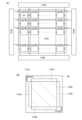
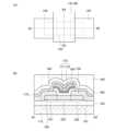
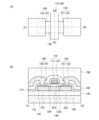
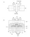
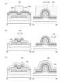
図1は、本発明の一態様の撮像装置の構成を示す断面図である。図1(A)に示す撮像装
置は、シリコン基板40に活性領域を有するトランジスタ51、酸化物半導体層を活性層
とするトランジスタ52およびトランジスタ53、ならびにシリコン基板40に設けられ
たフォトダイオード60を含む。各トランジスタおよびフォトダイオード60は、絶縁層
に埋め込まれた導電体70および各配線層と電気的な接続を有する。また、フォトダイオ
ード60のアノード61は、低抵抗領域63を介して導電体70と電気的な接続を有する
。1 is a cross-sectional view showing a configuration of an imaging device according to one embodiment of the present invention. The imaging device shown in Fig. 1A includes a
なお、低抵抗領域63はシリコン基板40に不純物を添加したp型領域で形成することが
できるが、図58(A)に示すように、金属を替わりに用いてもよい。また、図58(B
)に示すように、p型領域を貫通するように金属を設ける構成であってもよい。The
) a metal may be provided so as to penetrate the p-type region.
なお、上記要素における電気的な接続の形態は一例である。また、同一面上に設けられる
、または同一工程で設けられる配線および電極等は同一の符号を用い、代表する箇所のみ
に符号を付している。また、絶縁層に埋め込まれた導電体70については全体で同一の符
号を用いることとする。また、図面上では各配線、各電極、および導電体70を個別の要
素として図示しているが、それらが電気的に接続しているものについては、同一の要素と
して設けられる場合もある。The above-mentioned electrical connection forms of the elements are merely examples. The same reference numerals are used for wiring, electrodes, etc. that are provided on the same surface or in the same process, and only representative portions are labeled. The same reference numerals are used for the
また、当該撮像装置は、シリコン基板40に設けられたトランジスタ51、フォトダイオ
ード60および光制御層64を有する第1の層1100と、配線層71および絶縁層81
、82を有する第2の層1200と、トランジスタ52、トランジスタ53および絶縁層
83を有する第3の層1300と、配線層72、配線層73および絶縁層84、85を有
する第4の層1400を備えている。第1の層1100、第2の層1200、第3の層1
300、第4の層1400は当該順序で積層されている。The imaging device also includes a
, 82, a
300, and the
なお、上記各配線等の一部が設けられない場合や、上記以外の配線等やトランジスタ等が
各層に含まれる場合もある。また、上記以外の層が当該積層構造に含まれる場合もある。
また、上記の一部の層が含まれない場合もある。また、絶縁層81乃至絶縁層85は層間
絶縁膜としての機能を有する。Note that there may be cases where some of the above-mentioned wirings etc. are not provided, or where wirings etc., transistors etc. other than those described above are included in each layer, or where layers other than those described above are included in the laminate structure.
In addition, some of the above layers may not be included. The insulating layers 81 to 85 each function as an interlayer insulating film.
また、第1の層1100が有するフォトダイオード60の側面は光制御層64で囲まれて
いる。光制御層64は隣接するフォトダイオード間における素子分離層としても作用する
。フォトダイオード60の受光面から側面に向かって入射した光は光制御層64で反射ま
たは減衰させることができる。したがって、隣接する画素のフォトダイオード60に当該
光を侵入させることを防止するこができ、ノイズの少ない画像を得ることができる。Moreover, the side surface of the
光制御層64としては、シリコンよりも屈折率の低い材料を用いることが好ましい。例え
ば、酸化アルミニウム、酸化マグネシウム、酸化シリコン、酸化窒化シリコン、窒化酸化
シリコン、窒化シリコン、酸化ガリウム、酸化ゲルマニウム、酸化イットリウム、酸化ジ
ルコニウム、酸化ランタン、酸化ネオジム、酸化ハフニウム、または酸化タンタルなどの
絶縁体を用いることができる。また、アクリル樹脂やポリイミドなどの有機材料を用いて
もよい。シリコンよりも屈折率の低い材料を用いることで、フォトダイオード60の側面
に入射した光が全反射しやすくなる。また、上記材料の替わりに空気、窒素、酸素、アル
ゴン、ヘリウムなどの気体を用いても良く、この場合、大気圧よりも低い圧力としても良
い。As the
光制御層64としては、光を吸収しやすい材料を用いてもよい。例えば、カーボンブラッ
クなどのカーボン系黒色顔料、チタンブラックなどのチタン系黒色顔料、鉄の酸化物、銅
およびクロムの複合酸化物、銅、クロムおよび亜鉛の複合酸化物、などの材料が添加され
た樹脂などを用いることができる。A material that easily absorbs light may be used for the
なお、図58(C)に示すように、フォトダイオード60の側面の一部は光制御層64を
設けなくても良い。ここでは、低抵抗領域63にタングステン、タンタル、チタン、アル
ミニウムなどの金属を用いることで入射した光を反射させ、光制御層として機能させるこ
とができる。また、モリブデンやクロムなどの反射率の低い金属を用いてもよい。58C, a part of the side surface of the
また、図58(D)に示すように、光制御層64を貫通するように金属を設けてもよい。
なお、光制御層64中の金属の一部は、フォトダイオード60のアノード61と電気的に
接続することができる。Also, as shown in FIG. 58D, a metal may be provided so as to penetrate the
It should be noted that a part of the metal in the
また、図1(A)の一点鎖線A1-A2で示す部分(フォトダイオード部)の奥行方向の
上面図は、例えば、図59(A)、(B)、(C)、(D)、(E)、(F)に示すよう
な形態とすることができる。In addition, the top view in the depth direction of the portion (photodiode portion) indicated by the dashed dotted line A1-A2 in FIG. 1(A) can be, for example, in the form shown in FIGS. 59(A), (B), (C), (D), (E), and (F).
図59(A)はフォトダイオード60の受光部60pの上面形状が略四角形であり、その
周囲に光制御層64が設けられている。In FIG. 59A, the upper surface shape of a
図59(B)は受光部60pの上面形状が略四角形であり、その周囲に断片的に光制御層
64が設けられている。なお、図59(A)、(B)の受光部60pは略正方形で示して
いるが、略長方形、略台形などであってもよい。59B, the top surface shape of the
図59(C)は、図58(C)の構成におけるフォトダイオード部の上面図の一例である
。FIG. 59C is an example of a top view of a photodiode portion in the configuration of FIG.
図59(D)は受光部60pの上面形状が略六角形であり、その周囲に光制御層64が設
けられている。In FIG. 59D, the upper surface of a
図59(E)は受光部60pの上面形状が略三角形であり、その周囲に光制御層64が設
けられている。In FIG. 59E, the upper surface of a
図59(F)は受光部60pの上面形状が略円形であり、その周囲に光制御層64が設け
られている。In FIG. 59(F), the upper surface of a
なお、図59(C)乃至図59(F)に示した構成おいても、断片的に光制御層64が設
けられる構成としてもよい。また、受光部60pが上記以外の多角形や楕円形であっても
よい。59C to 59F, the
また、低抵抗領域63は、図58(B)に示すように金属を有した構成と置き換えること
ができる。また、光制御層64は、図58(D)に示すように、金属を有した構成と置き
換えることができる。The
上記のようにフォトダイオードの側面を光制御層64等で覆う構成であるため、様々な角
度からフォトダイオード60の側面に向かって入射する光をフォトダイオード60内に反
射、または減衰させることができる。Since the side surfaces of the
また、低抵抗領域63は、複数のフォトダイオード(複数の画素)で共有することができ
る。低抵抗領域63を共有することで配線等を少なくすることができる。例えば、図59
(A)に示すような受光部60pの上面形状が略四角形である場合は、図60(A)に示
すように、4個のフォトダイオードで低抵抗領域63を共有することができる。In addition, the
When the upper surface shape of the
また、図59(D)に示すような受光部60pの上面形状が略六角形である場合は、図6
0(B)に示すように、3個のフォトダイオードで低抵抗領域63を共有することができ
る。In addition, when the upper surface shape of the
As shown in FIG. 0(B), the
また、図59(E)に示すような受光部60pの上面形状が略三角形である場合は、図6
0(C)に示すように、6個のフォトダイオードで低抵抗領域63を共有することができ
る。In addition, when the upper surface shape of the
As shown in FIG. 0(C), six photodiodes can share a
なお、シリコン基板40はバルクのシリコン基板に限らず、SOI基板であってもよい。
また、シリコン基板40に替えて、ゲルマニウム、シリコンゲルマニウム、炭化シリコン
、ガリウムヒ素、アルミニウムガリウムヒ素、インジウムリン、窒化ガリウム、有機半導
体を材料とする基板を用いることもできる。The
Moreover, instead of the
上記積層構造において、トランジスタ51およびフォトダイオード60を有する第1の層
1100と、トランジスタ52およびトランジスタ53を有する第3の層1300との間
には絶縁層80が設けられる。In the above stacked structure, an insulating
トランジスタ51の活性領域近傍に設けられる絶縁層中の水素はシリコンのダングリング
ボンドを終端する。したがって、当該水素はトランジスタ51の信頼性を向上させる効果
がある。一方、トランジスタ52およびトランジスタ53等の活性層である酸化物半導体
層の近傍に設けられる絶縁層中の水素は、酸化物半導体中にキャリアを生成する要因の一
つとなる。そのため、当該水素はトランジスタ52およびトランジスタ53等の信頼性を
低下させる要因となる場合がある。したがって、シリコン系半導体材料を用いたトランジ
スタを有する一方の層と、酸化物半導体を用いたトランジスタを有する他方の層を積層す
る場合、これらの間に水素の拡散を防止する機能を有する絶縁層80を設けることが好ま
しい。絶縁層80により、一方の層に水素を閉じ込めることでトランジスタ51の信頼性
を向上することができる。また、一方の層から他方の層への水素の拡散が抑制されること
でトランジスタ52およびトランジスタ53等の信頼性も同時に向上させることができる
。Hydrogen in the insulating layer provided near the active region of the
絶縁層80としては、例えば酸化アルミニウム、酸化窒化アルミニウム、酸化ガリウム、
酸化窒化ガリウム、酸化イットリウム、酸化窒化イットリウム、酸化ハフニウム、酸化窒
化ハフニウム、イットリア安定化ジルコニア(YSZ)等を用いることができる。The insulating
Gallium oxynitride, yttrium oxide, yttrium oxynitride, hafnium oxide, hafnium oxynitride, yttria-stabilized zirconia (YSZ), or the like can be used.
上記トランジスタ52およびフォトダイオード60は回路91を形成し、トランジスタ5
1およびトランジスタ53は回路92を形成している。回路91は、画素回路として機能
させることができ、回路92は回路91を駆動するための駆動回路として機能させること
ができる。The
1 and the
回路91は、例えば、図1(B)に示す回路図のような構成とすることができる。トラン
ジスタ52のソースまたはドレインの一方とフォトダイオード60のカソード62が電気
的に接続され、トランジスタ52のソースまたはドレインの他方、トランジスタ54(図
1(A)に図示なし)のゲート、およびトランジスタ55(図1(A)に図示なし)のソ
ースまたはドレインの一方は電荷蓄積部(FD)と電気的に接続される。The
なお、電荷蓄積部は、具体的にはトランジスタ52およびトランジスタ53のソースまた
はドレインの空乏層容量、トランジスタ54のゲート容量、ならびに配線容量などで構成
される。Specifically, the charge storage portion is composed of the depletion layer capacitance of the source or drain of the
ここで、トランジスタ52は、フォトダイオード60の出力に応じて電荷蓄積部(FD)
の電位を制御するための転送トランジスタとしての機能を有することができる。また、ト
ランジスタ54は、電荷蓄積部(FD)の電位に応じた信号を出力する増幅トランジスタ
としての機能を有することができる。また、トランジスタ55は、電荷蓄積部(FD)の
電位を初期化するリセットトランジスタとしての機能を有することができる。Here, the
The
回路92は、例えば、図1(C)に示す回路図のようなCMOSインバータを含む構成と
することができる。トランジスタ51およびトランジスタ53のゲートは電気的に接続さ
れる。また、トランジスタ51のソースまたはドレインの一方は、トランジスタ53のソ
ースまたはドレインの一方と電気的に接続される。また、両方のトランジスタのソースま
たはドレインの他方はそれぞれ別の配線に電気的に接続される。すなわち、シリコン基板
に活性領域を有するトランジスタ51と酸化物半導体層を活性層とするトランジスタ53
でCMOS回路を形成する。The
A CMOS circuit is formed.
上記撮像装置において、シリコン基板40に活性領域を有するトランジスタ51はp-c
h型とし、酸化物半導体層を活性層とするトランジスタ52乃至トランジスタ55はn-
ch型とする。In the above-mentioned image pickup device, a
The
It is of type ch.
回路91においては、回路91に含まれる全てのトランジスタを第3の層1300に形成
することでその電気的な接続形態を容易にすることができ、作製工程を簡略化することが
できる。In the
また、酸化物半導体を有するトランジスタは極めて低いオフ電流特性を有するため、撮像
のダイナミックレンジを拡大することができる。図1(B)に示す回路構成では、フォト
ダイオード60に入射される光の強度が大きいときに電荷蓄積部(FD)の電位が小さく
なる。酸化物半導体を用いたトランジスタは極めてオフ電流が低いため、ゲート電位が極
めて小さい場合においても当該ゲート電位に応じた電流を正確に出力することができる。
したがって、検出することのできる照度のレンジ、すなわちダイナミックレンジを広げる
ことができる。In addition, since a transistor including an oxide semiconductor has extremely low off-state current characteristics, the dynamic range of imaging can be expanded. In the circuit configuration illustrated in FIG. 1B, when the intensity of light incident on the
Therefore, the range of detectable illuminance, that is, the dynamic range, can be expanded.
また、トランジスタ52およびトランジスタ55の低いオフ電流特性によって電荷蓄積部
(FD)で電荷を保持できる期間を極めて長くすることができる。そのため、回路構成や
動作方法を複雑にすることなく全画素で同時に電荷の蓄積動作を行うグローバルシャッタ
方式を適用することができる。したがって、被写体が動体であっても歪の小さい画像を容
易に得ることができる。また、グローバルシャッタ方式により露光時間(電荷の蓄積動作
を行う期間)を長くすることもできることから、低照度環境における撮像にも適する。In addition, the low off-current characteristics of the
また、酸化物半導体を用いたトランジスタは、シリコンを用いたトランジスタよりも電気
特性変動の温度依存性が小さいため、極めて広い温度範囲で使用することができる。した
がって、酸化物半導体を用いたトランジスタを有する撮像装置および半導体装置は、自動
車、航空機、宇宙機などへの搭載にも適している。Furthermore, a transistor using an oxide semiconductor has smaller temperature dependence of electrical characteristics than a transistor using silicon, and therefore can be used over an extremely wide temperature range. Therefore, imaging devices and semiconductor devices including a transistor using an oxide semiconductor are suitable for installation in automobiles, aircraft, spacecraft, and the like.
また、電荷蓄積部(FD)の電位を制御するためのトランジスタ52およびトランジスタ
55などはノイズの少ないトランジスタが好ましい。後述する二層または三層の酸化物半
導体層を有するトランジスタはチャネルが埋め込み型であり、極めてノイズに強い特性を
有する。したがって、当該トランジスタを用いることでノイズの少ない画像を得ることが
できる。In addition, the
また、回路91において、第1の層1100に設けるフォトダイオード60と、第3の層
1300に設けるトランジスタとを重なるように形成することができるため、画素の集積
度を高めることができる。すなわち、撮像装置の解像度を高めることができる。また、回
路91ではシリコン基板にはトランジスタが形成されていないため、フォトダイオードの
面積を広くすることができる。したがって、低照度環境においてもノイズの少ない画像を
得ることができる。In addition, in the
また、回路92においては、シリコン基板40に活性領域を有するn-ch型のトランジ
スタの工程が不要となるため、pウェルおよびn型不純物領域などの形成工程を省くこと
ができ、工程を大幅に削減することができる。また、CMOS回路のn-ch型トランジ
スタは前述した回路91に含まれるトランジスタと同時に作製することができる。Furthermore, in
図1に示す撮像装置は、シリコン基板40において、トランジスタ51が形成された面と
は逆側の面にフォトダイオード60の受光面を有する。したがって、各種トランジスタや
配線などの影響を受けずに光路を確保することができ、高開口率の画素を形成することが
できる。なお、フォトダイオード60の受光面をトランジスタ51が形成された面と同じ
とすることもできる。1 has a light receiving surface of a
また、本実施の形態における撮像装置が有するトランジスタおよびフォトダイオードの構
成は一例である。したがって、例えば、回路91を活性領域または活性層にシリコン等を
有するトランジスタで構成することもできる。また、回路92を活性層に酸化物半導体層
を有するトランジスタで構成することもできる。また、フォトダイオード60を非晶質シ
リコン層を光電変換層として構成することもできる。また、シリコン基板40に活性領域
を有するトランジスタ51をn-ch型とすることもできる。The configurations of the transistors and photodiodes included in the imaging device in this embodiment are just an example. Therefore, for example, the
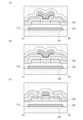
図2(A)は、図1(A)に示す撮像装置にカラーフィルタ等を付加した形態の一例の断
面図である。当該断面図は、3画素分の回路91を有する領域(領域91a、領域91b
、領域91c)、および回路92の一部を有する領域92aを示している。第1の層11
00に形成されるフォトダイオード60上には絶縁層1500が形成される。絶縁層15
00は可視光に対して透光性の高い酸化シリコン膜などを用いることができる。また、パ
ッシベーション膜として窒化シリコン膜を積層する構成としてもよい。また、反射防止膜
として、酸化ハフニウムなどの誘電体膜を積層する構成としてもよい。なお、図56(A
)に示すように、絶縁層1500を設けない構成とすることもできる。2A is a cross-sectional view of an example of a configuration in which a color filter or the like is added to the imaging device shown in FIG.
,
An insulating
For the 00, a silicon oxide film or the like having high transparency to visible light can be used. Also, a silicon nitride film may be laminated as a passivation film. Also, a dielectric film such as hafnium oxide may be laminated as an anti-reflection film.
), a configuration in which the insulating
絶縁層1500上には、遮光層1510が形成される。遮光層1510は、上部のカラー
フィルタを通る光の混色を防止する作用を有する。また、領域92a上における遮光層1
510は、シリコン基板40に活性領域を有するトランジスタの光照射による特性変動を
防止する作用も有する。遮光層1510には、アルミニウム、タングステンなどの金属層
や当該金属層と反射防止膜としての機能を有する誘電体膜を積層する構成とすることがで
きる。なお、図56(B)に示すように、遮光層1510を設けない構成とすることもで
きる。A light-
The
絶縁層1500および遮光層1510上には平坦化膜として有機樹脂層1520が形成さ
れ、領域91a、領域91bおよび領域91c上においてそれぞれカラーフィルタ153
0a、カラーフィルタ1530bおよびカラーフィルタ1530cが対になるように形成
される。カラーフィルタ1530a、カラーフィルタ1530bおよびカラーフィルタ1
530cには、それぞれR(赤)、G(緑)、B(青)などの色を割り当てることにより
、カラー画像を得ることができる。なお、図56(C)に示すように、有機樹脂層152
0を設けない構成とすることもできる。また、図56(D)に示すように、絶縁層150
0、遮光層1510、有機樹脂層1520を設けない構成とすることもできる。また、図
示はしないが、絶縁層1500、遮光層1510、有機樹脂層1520のいずれか二つを
設けない構成とすることもできる。An
The
A color image can be obtained by allocating colors such as R (red), G (green), and B (blue) to the
Alternatively, the insulating
Alternatively, the insulating
カラーフィルタ1530a、カラーフィルタ1530bおよびカラーフィルタ1530c
上にはマイクロレンズアレイ1540が設けられる。したがって、マイクロレンズアレイ
1540が有する個々のレンズを通る光が直下のカラーフィルタを通り、フォトダイオー
ドに照射されるようになる。
A
また、図57(A)に示すように、それぞれのカラーフィルタの間に遮光層1510を設
けてもよい。As shown in FIG. 57A, a light-
また、図57(B)に示すように、マイクロレンズアレイ1540における各レンズの境
界を覆うように遮光層1510を設けてもよい。As shown in FIG. 57B, a light-
また、図57(C)に示すように、遮光層1510を省いて、光制御層64がそれぞれの
カラーフィルタの間にまで延在する構成としてもよい。Also, as shown in FIG. 57C, the
また、図57(D)に示すように、遮光層1510を省いて、光制御層64がマイクロレ
ンズアレイ1540における各レンズの間にまで延在する構成としてもよい。Also, as shown in FIG. 57D, the
また、光制御層64は図61(A)に示すように、フォトダイオード60の深さ方向全体
ではなく、受光面に近い側の一部においてフォトダイオード60の側面を覆うように形成
されていてもよい。また、図61(B)に示すように、受光面から遠い側の一部において
フォトダイオード60の側面を覆うように形成されていてもよい。なお、領域66はシリ
コン基板40の一部であり、フォトダイオード60の構成の一部となっていてもよい。61A, the
また、図62(A)にフォトダイオード60および光制御層64の上面図を示す。図62
(B)に遮光層1510の上面図を示す。図62(C)にカラーフィルタ1530の上面
図を示す。図62(D)は、図62(A)、(B)、(C)および回路91に含まれるト
ランジスタ50を重ねて図示したものである。回路91に含まれるトランジスタ50はフ
ォトダイオード60と重ねて形成することができるため、フォトダイオード60の開口率
を高くすることができる。62A shows a top view of the
Fig. 62B shows a top view of the light-
第4の層1400には支持基板1600が接して設けられる。支持基板1600としては
、シリコン基板などの半導体基板、ガラス基板、金属基板、セラミック基板などの硬質基
板を用いることができる。なお、第4の層1400と支持基板1600との間には接着層
となる無機絶縁層や有機樹脂層が形成されていてもよい。A supporting
なお、回路91および回路92と、外部の電源回路や制御回路等とは、第4の層1400
における配線層72または配線層73を用いて接続すればよい。The
The connection may be made using the
上記撮像装置の構成において、カラーフィルタ1530a、カラーフィルタ1530bお
よびカラーフィルタ1530cの代わりに光学変換層1550(図2(B)参照)を用い
ることにより様々な波長領域における画像が得られる撮像装置とすることができる。In the above-described configuration of the imaging device, an optical conversion layer 1550 (see FIG. 2B) can be used instead of the
例えば、光学変換層1550に可視光線の波長以下の光を遮るフィルタを用いれば赤外線
撮像装置とすることができる。また、光学変換層1550に近赤外線の波長以下の光を遮
るフィルタを用いれば遠赤外線撮像装置とすることができる。また、光学変換層1550
に可視光線の波長以上の光を遮るフィルタを用いれば紫外線撮像装置とすることができる
。For example, if a filter that blocks light having a wavelength equal to or shorter than visible light is used in the
If a filter that blocks light with wavelengths longer than visible light is used, an ultraviolet imaging device can be created.
なお、赤外線撮像装置とする場合には、フォトダイオード60の光電変換層のバンドギャ
ップが狭くなるようにゲルマニウムを添加し、赤外線に対する感度を向上させてもよい。
また、紫外線撮像装置とする場合には、バンドギャップの広い酸化物半導体層などを光電
変換層に用い、紫外線に対する感度を向上させてもよい。When used as an infrared imaging device, germanium may be added to the photoelectric conversion layer of the
In the case of an ultraviolet imaging device, an oxide semiconductor layer having a wide band gap or the like may be used for the photoelectric conversion layer to improve sensitivity to ultraviolet rays.
また、光学変換層1550にシンチレータを用いれば、X線撮像装置などに用いる、放射
線の強弱を可視化した画像を得る撮像装置とすることができる。被写体を透過したX線等
の放射線がシンチレータに入射されると、フォトルミネッセンスと呼ばれる現象により可
視光線や紫外光線などの光(蛍光)に変換される。そして、当該光をフォトダイオード6
0で検知することにより画像データを取得する。また、放射線検出器などに当該構成の撮
像装置を用いてもよい。Furthermore, if a scintillator is used for the
Image data is obtained by detecting at 0. Also, an imaging device having this configuration may be used as a radiation detector or the like.
シンチレータは、X線やガンマ線などの放射線が照射されると、そのエネルギーを吸収し
て可視光や紫外光を発する物質、または当該物質を含む材料からなる。例えば、Gd2O
2S:Tb、Gd2O2S:Pr、Gd2O2S:Eu、BaFCl:Eu、NaI、C
sI、CaF2、BaF2、CeF3、LiF、LiI、ZnOなどの材料や、それらを
樹脂やセラミクスに分散させたものが知られている。A scintillator is made of a substance that absorbs the energy of radiation such as X-rays or gamma rays and emits visible light or ultraviolet light when irradiated with theradiation , or a material that contains such a substance.
2S :Tb,Gd2O2S: Pr,Gd2O2S :Eu, BaFCl:Eu, NaI,C
Known materials include sI,CaF2 , BaF2,CeF3 , LiF, LiI, ZnO, and materials obtained by dispersing these in resins or ceramics.
図3は撮像装置の構成を示す概念図である。回路91を有する画素マトリクス1700の
側部に回路1730および回路1740が配置される。回路1730は、例えば、リセッ
トトランジスタの駆動回路として作用させることができる。この場合、回路1730と図
1(B)におけるトランジスタ55とが電気的に接続される。回路1740は、例えば、
転送トランジスタの駆動回路として作用させることができる。この場合、回路1740と
図1(B)におけるトランジスタ52とが電気的に接続される。なお、図3では回路17
30および回路1740を分割して配置する構成を図示しているが、一つの領域に回路1
730および回路1740がまとめて配置される構成としてもよい。3 is a conceptual diagram showing the configuration of an imaging device. A
The
Although the
730 and
また、画素マトリクス1700には回路1750が接続される。回路1750は、例えば
、トランジスタ54と電気的に接続される垂直出力線を選択する駆動回路として機能させ
ることができる。In addition, a
また、画素マトリクス1700には回路1760が接続されてもよい。回路1760は、
例えば、回路1750を分割した回路、電源回路または記憶回路などの機能を有すること
ができる。なお、回路1760を設けない構成とすることもできる。A
For example, the
上記各回路の具体的な位置関係の一例を図3(B)に示す。例えば、回路1730、回路
1740、回路1750、回路1760のそれぞれは、例えば4つの領域に設けられる。
なお、それぞれの回路の位置および占有面積は図示した例に限られない。そして、これら
の回路が配置される領域の内側に画素マトリクス1700が設けられる。回路1730、
回路1740、回路1750、回路1760および画素マトリクス1700が有する画素
回路のそれぞれと接続される信号線および電源線等は、シリコン基板40に形成される配
線と電気的に接続される。また、当該配線はシリコン基板40の周囲に形成される端子1
770と電気的に接続される。シリコン基板40に形成される端子1770はワイヤボン
ディング等で外部の回路と電気的に接続することができる。3B shows a specific example of the positional relationship between the circuits. For example, each of the
The positions and the areas occupied by the respective circuits are not limited to those shown in the figures. The
Signal lines, power supply lines, and the like connected to the
The terminal 1770 formed on the
回路1730および回路1740は、”Low”または”High”の2値出力の駆動回
路である。したがって、図4(A)で示すようにシフトレジスタ1800とバッファ回路
1900の組み合わせで駆動することができる。The
また、回路1750は、図4(B)に示すようにシフトレジスタ1810とバッファ回路
1910とアナログスイッチ2100によって構成することができる。各垂直出力線21
10をアナログスイッチ2100によって選択し、選択された垂直出力線2110の電位
を出力線2200に出力する。アナログスイッチ2100はシフトレジスタ1810とバ
ッファ回路1910で順次選択していくものとする。As shown in FIG. 4B, the
10 is selected by an
本発明の一態様では、回路1730、回路1740および回路1750の全てまたは一部
に回路92を含んだ構成とする。すなわち、上記シフトレジスタ1800、バッファ回路
1900、シフトレジスタ1810、バッファ回路1910、およびアナログスイッチ2
100の全てまたはいずれかはシリコン基板40に活性領域を有するp-ch型トランジ
スタと酸化物半導体層を活性層とするn-ch型トランジスタで形成されるCMOS回路
を有する。In one embodiment of the present invention, the
All or any of the elements 100 has a CMOS circuit formed of a p-ch type transistor having an active region in a
なお、本実施の形態において、本発明の一態様について述べた。または、他の実施の形態
において、本発明の一態様について述べる。ただし、本発明の一態様は、これらに限定さ
れない。例えば、本発明の一態様として、撮像装置に適用した場合の例を示したが、本発
明の一態様は、これに限定されない。場合によっては、または、状況に応じて、本発明の
一態様は、撮像装置に適用しなくてもよい。例えば、本発明の一態様は、別の機能を有す
る半導体装置に適用してもよい。Note that one embodiment of the present invention has been described in this embodiment. Alternatively, one embodiment of the present invention will be described in another embodiment. However, one embodiment of the present invention is not limited thereto. For example, although an example in which the present invention is applied to an imaging device has been described as one embodiment of the present invention, one embodiment of the present invention is not limited thereto. In some cases or depending on the situation, one embodiment of the present invention does not need to be applied to an imaging device. For example, one embodiment of the present invention may be applied to a semiconductor device having another function.
本実施の形態は、他の実施の形態に記載した構成と適宜組み合わせて実施することが可能
である。This embodiment mode can be implemented in appropriate combination with structures described in other embodiment modes.
(実施の形態2)
本実施の形態では、実施の形態1で説明した回路91ついて説明する。(Embodiment 2)
In this embodiment mode, the
図1(B)に示す回路91および各種配線との接続形態の詳細を図5(A)に示す。図5
(A)に示す回路は、フォトダイオード60、トランジスタ52、トランジスタ54、ト
ランジスタ55およびトランジスタ56を含んだ構成となっている。FIG. 5A shows the details of the
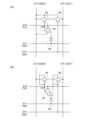
The circuit shown in (A) includes a
フォトダイオード60のアノードは配線316に接続され、カソードはトランジスタ52
のソースまたはドレインの一方と接続される。トランジスタ52のソースまたはドレイン
の他方は電荷蓄積部(FD)と接続され、ゲートは配線312(TX)と接続される。ト
ランジスタ54のソースまたはドレインの一方は配線314(GND)と接続され、ソー
スまたはドレインの他方はトランジスタ56のソースまたはドレインの一方と接続され、
ゲートは電荷蓄積部(FD)と接続される。トランジスタ55のソースまたはドレインの
一方は電荷蓄積部(FD)と接続され、ソースまたはドレインの他方は配線317と接続
され、ゲートは配線311(RS)と接続される。トランジスタ56のソースまたはドレ
インの他方は配線315(OUT)と接続され、ゲートは配線313(SE)に接続され
る。なお、上記接続は全て電気的な接続とする。The anode of the
The other of the source and drain of the
The gate is connected to the charge storage portion (FD). One of the source and drain of the
なお、配線314には、GND、VSS、VDDなどの電位が供給されていてもよい。こ
こで、電位や電圧は相対的なものである。そのため、GNDの電位の大きさは、必ずしも
、0ボルトであるとは限らないものとする。Note that a potential such as GND, VSS, or VDD may be supplied to the
フォトダイオード60は受光素子であり、画素回路に入射した光に応じた電流を生成する
機能を有することができる。トランジスタ52は、フォトダイオード60による電荷蓄積
部(FD)への電荷蓄積を制御する機能を有することができる。トランジスタ54は、電
荷蓄積部(FD)の電位に応じた信号を出力する動作を行う機能を有することができる。
トランジスタ55は、電荷蓄積部(FD)の電位のリセットする動作を行う機能を有する
ことができる。トランジスタ56は、読み出し時に画素回路の選択を制御する動作を行う
機能を有することができる。The
The
なお、電荷蓄積部(FD)は、電荷保持ノードであり、フォトダイオード60が受ける光
の量に応じて変化する電荷を保持する。The charge storage section (FD) is a charge holding node, and holds a charge that changes depending on the amount of light received by the
なお、トランジスタ54とトランジスタ56とは、配線315と配線314との間で、直
列接続されることができる。配線314、トランジスタ54、トランジスタ56、配線3
15の順で並んでもよいし、配線314、トランジスタ56、トランジスタ54、配線3
15の順で並んでもよい。The
Alternatively, the
They may be arranged in the order of 15.
配線311(RS)は、トランジスタ55を制御するための信号線としての機能を有する
ことができる。配線312(TX)は、トランジスタ52を制御するための信号線として
の機能を有することができる。配線313(SE)は、トランジスタ56を制御するため
の信号線としての機能を有することができる。配線314(GND)は、基準電位(例え
ばGND)を設定する信号線としての機能を有することができる。配線315(OUT)
は、トランジスタ54から出力される信号を読み出すための信号線としての機能を有する
ことができる。配線316はフォトダイオード60を介して電荷蓄積部(FD)から電荷
を出力するための信号線としての機能を有することができ、図5(A)の回路においては
低電位線である。また、配線317は電荷蓄積部(FD)の電位をリセットするための信
号線としての機能を有することができ、図5(A)の回路においては高電位線である。The wiring 311 (RS) can function as a signal line for controlling the
can function as a signal line for reading out a signal output from the
また、回路91は、図5(B)に示す構成であってもよい。図5(B)に示す回路は、図
5(A)に示す回路と構成要素は同じであるが、フォトダイオード60のアノードがトラ
ンジスタ52のソースまたはドレインの一方と電気的に接続され、フォトダイオード60
のカソードが配線316と電気的に接続される点で異なる。この場合、配線316はフォ
トダイオード60を介して電荷蓄積部(FD)に電荷を供給するための信号線としての機
能を有し、図5(B)の回路においては高電位線となる。また、配線317は低電位線と
なる。The
5B in that the cathode of the
次に、図5(A)、(B)に示す各素子の構成について説明する。Next, we will explain the configuration of each element shown in Figures 5 (A) and (B).
フォトダイオード60には、シリコン基板においてpn型やpin型の接合が形成された
素子を用いることができる。The
トランジスタ52、トランジスタ54、トランジスタ55、およびトランジスタ56は、
非晶質シリコン、微結晶シリコン、多結晶シリコン、単結晶シリコンなどのシリコン半導
体を用いて形成することも可能であるが、酸化物半導体を用いたトランジスタで形成する
ことが好ましい。酸化物半導体でチャネル形成領域を形成したトランジスタは、極めてオ
フ電流が低い特性を示す特徴を有している。The
Although a silicon semiconductor such as amorphous silicon, microcrystalline silicon, polycrystalline silicon, or single crystal silicon can be used, a transistor using an oxide semiconductor is preferable. A transistor in which a channel formation region is formed using an oxide semiconductor has an extremely low off-state current.
特に、電荷蓄積部(FD)と接続されているトランジスタ52およびトランジスタ55の
リーク電流が大きいと、電荷蓄積部(FD)に蓄積された電荷が保持できる時間が十分で
なくなる。したがって、少なくとも当該二つのトランジスタに酸化物半導体を用いたトラ
ンジスタを使用することで、電荷蓄積部(FD)からの不要な電荷の流出を防止すること
ができる。In particular, when the leakage current of the
また、トランジスタ54およびトランジスタ56においても、リーク電流が大きいと、配
線314または配線315に不必要な電荷の出力が起こるため、これらのトランジスタと
して、酸化物半導体でチャネル形成領域を形成したトランジスタを用いることが好ましい
。In addition, in the
図5(A)の回路の動作の一例について図6(A)に示すタイミングチャートを用いて説
明する。An example of the operation of the circuit in FIG. 5A will be described with reference to a timing chart shown in FIG.
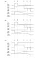
図6(A)では簡易に説明するため、各配線の電位は、二値変化する信号として与える。
ただし、各電位はアナログ信号であるため、実際には状況に応じて二値に限らず種々の値
を取り得る。なお、図に示す信号701は配線311(RS)の電位、信号702は配線
312(TX)の電位、信号703は配線313(SE)の電位、信号704は電荷蓄積
部(FD)の電位、信号705は配線315(OUT)の電位に相当する。なお、配線3
16の電位は常時”Low”、配線317の電位は常時”High”とする。For ease of explanation, the potential of each wiring is given as a signal that changes into two values in FIG.
However, since each potential is an analog signal, it can take various values, not limited to two values, depending on the situation. Note that the
The potential of the
時刻Aにおいて、配線311の電位(信号701)を”High”、配線312の電位(
信号702)を”High”とすると、電荷蓄積部(FD)の電位(信号704)は配線
317の電位(”High”)に初期化され、リセット動作が開始される。なお、配線3
15の電位(信号705)は、”High”にプリチャージしておく。At time A, the potential of the wiring 311 (signal 701) is set to “High” and the potential of the wiring 312 (
When the potential (signal 702) of the charge storage unit (FD) is set to "High", the potential (signal 704) of the charge storage unit (FD) is initialized to the potential ("High") of the
The potential of No. 15 (signal 705) is precharged to "High".
時刻Bにおいて、配線311の電位(信号701)を”Low”とするとリセット動作が
終了し、蓄積動作が開始される。ここで、フォトダイオード60には逆方向バイアスが印
加されるため、逆方向電流により、電荷蓄積部(FD)の電位(信号704)が低下し始
める。フォトダイオード60は、光が照射されると逆方向電流が増大するので、照射され
る光の量に応じて電荷蓄積部(FD)の電位(信号704)の低下速度は変化する。すな
わち、フォトダイオード60に照射する光の量に応じて、トランジスタ54のソースとド
レイン間のチャネル抵抗が変化する。At time B, when the potential (signal 701) of the
時刻Cにおいて、配線312の電位(信号702)を”Low”とすると蓄積動作が終了
し、電荷蓄積部(FD)の電位(信号704)は一定となる。ここで、当該電位は、蓄積
動作中にフォトダイオード60が生成した電荷量により決まる。すなわち、フォトダイオ
ード60に照射されていた光の量に応じて変化する。また、トランジスタ52およびトラ
ンジスタ55は、酸化物半導体層でチャネル形成領域を形成したオフ電流が極めて低いト
ランジスタで構成されているため、後の選択動作(読み出し動作)を行うまで、電荷蓄積
部(FD)の電位を一定に保つことが可能である。At time C, when the potential of the wiring 312 (signal 702) is set to "low," the accumulation operation ends, and the potential of the charge accumulation portion (FD) (signal 704) becomes constant. Here, the potential is determined by the amount of charge generated by the
なお、配線312の電位(信号702)を”Low”とする際に、配線312と電荷蓄積
部(FD)との間における寄生容量により、電荷蓄積部(FD)の電位に変化が生じるこ
とがある。当該電位の変化量が大きい場合は、蓄積動作中にフォトダイオード60が生成
した電荷量を正確に取得できないことになる。当該電位の変化量を低減するには、トラン
ジスタ52のゲート-ソース(もしくはゲート-ドレイン)間容量を低減する、トランジ
スタ54のゲート容量を増大する、電荷蓄積部(FD)に保持容量を設ける、などの対策
が有効である。なお、本実施の形態では、これらの対策により当該電位の変化を無視でき
るものとしている。When the potential of the wiring 312 (signal 702) is set to "Low", a change in the potential of the charge storage unit (FD) may occur due to parasitic capacitance between the
時刻Dに、配線313の電位(信号703)を”High”にすると、トランジスタ56
が導通して選択動作が開始され、配線314と配線315が、トランジスタ54とトラン
ジスタ56とを介して導通する。そして、配線315の電位(信号705)は、低下して
いく。なお、配線315のプリチャージは、時刻D以前に終了しておけばよい。ここで、
配線315の電位(信号705)が低下する速さは、トランジスタ54のソースとドレイ
ン間の電流に依存する。すなわち、蓄積動作中にフォトダイオード60に照射されている
光の量に応じて変化する。At time D, when the potential of the wiring 313 (signal 703) is set to “High”, the
is turned on, the selection operation is started, and the
The speed at which the potential of the wiring 315 (signal 705) decreases depends on the current between the source and drain of the
時刻Eにおいて、配線313の電位(信号703)を”Low”にすると、トランジスタ
56が遮断されて選択動作は終了し、配線315の電位(信号705)は、一定となり、
その値はフォトダイオード60に照射されていた光の量に応じて変化する。したがって、
配線315の電位を取得することで、蓄積動作中にフォトダイオード60に照射されてい
た光の量を知ることができる。At time E, when the potential of the wiring 313 (signal 703) is set to “Low”, the
The value changes depending on the amount of light that is irradiated onto the
By acquiring the potential of the
より具体的には、フォトダイオード60に照射されている光が強いと、電荷蓄積部(FD
)の電位、すなわちトランジスタ54のゲート電圧は低下する。そのため、トランジスタ
54のソース-ドレイン間に流れる電流は小さくなり、配線315の電位(信号705)
はゆっくりと低下する。したがって、配線315からは比較的高い電位を読み出すことが
できる。More specifically, when the light irradiating the
), that is, the gate voltage of the
Therefore, a relatively high potential can be read out from the
逆に、フォトダイオード60に照射されている光が弱いと、電荷蓄積部(FD)の電位、
すなわち、トランジスタ54のゲート電圧は高くなる。そのため、トランジスタ54のソ
ース-ドレイン間に流れる電流は大きくなり、配線315の電位(信号705)は速く低
下する。したがって、配線315からは比較的低い電位を読み出すことができる。Conversely, when the light irradiated to the
That is, the gate voltage of the
次に、図5(B)の回路の動作の例について図6(B)に示すタイミングチャートを用い
て説明する。なお、配線316の電位は常時”High”、配線317の電位は常時”L
ow”とする。Next, an example of the operation of the circuit in FIG. 5B will be described with reference to a timing chart shown in FIG. 6B. Note that the potential of the
ow".
時刻Aにおいて、配線311の電位(信号701)を”High”、配線312の電位(
信号702)を”High”とすると、電荷蓄積部(FD)の電位(信号704)は配線
317の電位(”Low”)に初期化され、リセット動作が開始される。なお、配線31
5の電位(信号705)は、”High”にプリチャージしておく。At time A, the potential of the wiring 311 (signal 701) is set to “High” and the potential of the wiring 312 (
When the potential (signal 702) of the charge storage unit (FD) is set to "High", the potential (signal 704) of the charge storage unit (FD) is initialized to the potential ("Low") of the
The potential of No. 5 (signal 705) is precharged to "High".
時刻Bにおいて、配線311の電位(信号701)を”Low”とするとリセット動作が
終了し、蓄積動作が開始される。ここで、フォトダイオード60には逆方向バイアスが印
加されるため、逆方向電流により、電荷蓄積部(FD)の電位(信号704)が上昇し始
める。At time B, when the potential (signal 701) of the
時刻C以降の動作は、図6(A)のタイミングチャートの説明を参照することができ、時
刻Eにおいて、配線315の電位を取得することで、蓄積動作中にフォトダイオード60
に照射されていた光の量を知ることができる。The operation after time C can be explained with reference to the timing chart in FIG. 6A. At time E, the potential of the
This allows you to know the amount of light that was being irradiated onto the object.
また、回路91は、図7(A)、(B)に示す構成であってもよい。The
図7(A)に示す回路は、図5(A)に示す回路の構成からトランジスタ55、配線31
6および配線317を省いた構成であり、配線311(RS)はフォトダイオード60の
アノードに電気的に接続される。その他の構成は、図5(A)に示す回路と同じである。The circuit shown in FIG. 7A is the same as the circuit shown in FIG.
5A. The wiring 311 (RS) is electrically connected to the anode of the
図7(B)に示す回路は、図7(A)に示す回路と構成要素は同じであるが、フォトダイ
オード60のアノードがトランジスタ52のソースまたはドレインの一方と電気的に接続
され、フォトダイオード60のカソードが配線311(RS)と電気的に接続される点で
異なる。The circuit shown in FIG. 7B has the same components as the circuit shown in FIG. 7A, but differs in that the anode of the
図7(A)の回路は図5(A)の回路と同様に、図6(A)に示すタイミングチャートで
動作させることができる。The circuit in FIG. 7A can be operated according to the timing chart shown in FIG. 6A, similarly to the circuit in FIG. 5A.
時刻Aにおいて、配線311の電位(信号701)を”High”、配線312の電位(
信号702)を”High”とすると、フォトダイオード60に順方向バイアスが印加さ
れ、電荷蓄積部(FD)の電位(信号704)が”High”となる。すなわち、電荷蓄
積部(FD)の電位は配線311(RS)の電位(”High”)に初期化され、リセッ
ト状態となる。以上がリセット動作の開始である。なお、配線315の電位(信号705
)は、”High”にプリチャージしておく。At time A, the potential of the wiring 311 (signal 701) is set to “High” and the potential of the wiring 312 (
When the potential (signal 702) of the wiring 315 (RS) is set to "High", a forward bias is applied to the
) is precharged to "High".
時刻Bにおいて、配線311の電位(信号701)を”Low”とするとリセット動作が
終了し、蓄積動作が開始される。ここで、フォトダイオード60には逆方向バイアスが印
加されるため、逆方向電流により、電荷蓄積部(FD)の電位(信号704)が低下し始
める。At time B, when the potential (signal 701) of the
時刻C以降の動作は、図5(A)の回路動作の説明を参照することができ、時刻Eにおい
て、配線315の電位を取得することで、蓄積動作中にフォトダイオード60に照射され
ていた光の量を知ることができる。For the operation after time C, the explanation of the circuit operation in Figure 5 (A) can be referred to. At time E, by acquiring the potential of the
図7(B)の回路は、図6(C)に示すタイミングチャートで動作させることができる。The circuit in Figure 7(B) can be operated according to the timing chart shown in Figure 6(C).
時刻Aにおいて、配線311の電位(信号701)を”Low”、配線312の電位(信
号702)を”High”とすると、フォトダイオード60に順方向バイアスが印加され
、電荷蓄積部(FD)の電位(信号704)が”Low”のリセット状態となる。以上が
リセット動作の開始である。なお、配線315の電位(信号705)は、”High”に
プリチャージしておく。At time A, when the potential (signal 701) of the
時刻Bにおいて、配線311の電位(信号701)を”High”とするとリセット動作
が終了し、蓄積動作が開始される。ここで、フォトダイオード60には逆方向バイアスが
印加されるため、逆方向電流により、電荷蓄積部(FD)の電位(信号704)が上昇し
始める。At time B, when the potential (signal 701) of the
時刻C以降の動作は、図5(A)の回路動作の説明を参照することができ、時刻Eにおい
て、配線315の電位を取得することで、蓄積動作中にフォトダイオード60に照射され
ていた光の量を知ることができる。For the operation after time C, the explanation of the circuit operation in Figure 5 (A) can be referred to. At time E, by acquiring the potential of the
なお、図5(A)、(B)および図7(A)、(B)では、トランジスタ52が設けられ
ている場合の例を示したが、本発明の一態様は、これに限定されない。図8(A)、(B
)に示すように、トランジスタ52を省くことも可能である。Note that although the example in which the
It is also possible to omit
また、回路91に用いるトランジスタは、図9(A)または図9(B)に示すように、ト
ランジスタ52、トランジスタ54、およびトランジスタ56にバックゲートを設けた構
成であってもよい。図9(A)はバックゲートに定電位を印加する構成であり、しきい値
電圧を制御することができる。また、図9(B)はフロントゲートと同じ電位がバックゲ
ートに印加される構成であり、オン電流を増加させることができる。なお、図9(A)に
おいては、バックゲートが配線314(GND)と電気的に接続される構成を例示したが
、定電位が供給される別の配線と電気的に接続されていてもよい。なお、図9(A)、(
B)は図7(A)に示す回路においてトランジスタにバックゲートを設けた例を示したが
、同様の構成を図5(A)、(B)、図7(B)、図8(A)、(B)に示す回路にも適
用することもできる。また、一つの回路に含まれるトランジスタに対し、フロントゲート
と同じ電位がバックゲートに印加される構成、バックゲートに定電位を印加する構成、ま
たはバックゲートを設けない構成を必要に応じて任意に組み合わせた回路構成としてもよ
い。The transistors used in the
7A and 7B) shows an example in which a back gate is provided to a transistor in the circuit shown in FIG 7A, but a similar configuration can also be applied to the circuits shown in FIG 5A, FIG 5B, FIG 7B, FIG 8A, and FIG 8B. In addition, a circuit configuration in which the same potential as that of the front gate is applied to the back gate of a transistor included in one circuit, a constant potential is applied to the back gate, or a configuration in which a back gate is not provided may be arbitrarily combined as necessary.
なお、上述した回路例において、配線315(OUT)には、図10(A)、(B)、(
C)に示すような積分回路が接続されていてもよい。当該回路によって、読み出し信号の
S/N比を高めることができ、より微弱な光を検出することができる。すなわち、撮像装
置の感度を高めることができる。In the above-described circuit example, the wiring 315 (OUT) is
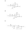
An integrating circuit as shown in FIG. 3C may be connected. This circuit can increase the S/N ratio of the read signal, making it possible to detect weaker light. In other words, the sensitivity of the imaging device can be increased.
図10(A)は、演算増幅回路(OPアンプともいう)を用いた積分回路である。演算増
幅回路の反転入力端子は、抵抗素子Rを介して配線315(OUT)に接続される。演算
増幅回路の非反転入力端子は、接地電位に接続される。演算増幅回路の出力端子は、容量
素子Cを介して演算増幅回路の反転入力端子に接続される。10A shows an integrating circuit using an operational amplifier circuit (also called an OP amplifier). The inverting input terminal of the operational amplifier circuit is connected to a wiring 315 (OUT) via a resistor R. The non-inverting input terminal of the operational amplifier circuit is connected to a ground potential. The output terminal of the operational amplifier circuit is connected to the inverting input terminal of the operational amplifier circuit via a capacitor C.
図10(B)は、図10(A)とは異なる構成の演算増幅回路を用いた積分回路である。
演算増幅回路の反転入力端子は、抵抗素子Rと容量素子C1を介して配線315(OUT
)に接続される。演算増幅回路の非反転入力端子は、接地電位に接続される。演算増幅回
路の出力端子は、容量素子C2を介して演算増幅回路の反転入力端子に接続される。FIG. 10B shows an integrating circuit using an operational amplifier circuit having a different configuration from that shown in FIG.
The inverting input terminal of the operational amplifier circuit is connected to a wiring 315 (OUT
The non-inverting input terminal of the operational amplifier circuit is connected to the ground potential. The output terminal of the operational amplifier circuit is connected to the inverting input terminal of the operational amplifier circuit via the capacitive element C2.
図10(C)は、図10(A)および図10(B)とは異なる構成の演算増幅回路を用い
た積分回路である。演算増幅回路の非反転入力端子は、抵抗素子Rを介して配線315(
OUT)に接続される。演算増幅回路の出力端子は、演算増幅回路の反転入力端子に接続
される。なお、抵抗素子Rと容量素子Cは、CR積分回路を構成する。また、演算増幅回
路はユニティゲインバッファを構成する。FIG. 10C shows an integrating circuit using an operational amplifier circuit having a different configuration from those shown in FIG. 10A and FIG. 10B. The non-inverting input terminal of the operational amplifier circuit is connected to a wiring 315 (
The output terminal of the operational amplifier circuit is connected to an inverting input terminal of the operational amplifier circuit. The resistive element R and the capacitive element C form a CR integrating circuit. The operational amplifier circuit forms a unity gain buffer.
本実施の形態は、他の実施の形態に記載した構成と適宜組み合わせて実施することが可能
である。This embodiment mode can be implemented in appropriate combination with structures described in other embodiment modes.
(実施の形態3)
本実施の形態では、電荷蓄積部(FD)の電位を初期化するトランジスタ、電荷蓄積部(
FD)の電位に応じた信号を出力するトランジスタ、および各配線(信号線)を画素間(
回路91間)で兼用する場合の回路構成について説明する。(Embodiment 3)
In this embodiment, a transistor that initializes the potential of the charge storage unit (FD),
A transistor that outputs a signal according to the potential of the FD, and each wiring (signal line) is connected between pixels (
A circuit configuration in which the two circuits are used together will be described.
図11に示す画素回路は、図5(A)に示す回路と同様にトランジスタ52(転送トラン
ジスタとして機能)、トランジスタ54(増幅トランジスタとして機能)、トランジスタ
55(リセットトランジスタとして機能)、トランジスタ56(選択トランジスタとして
機能)、およびフォトダイオード60を各画素に一つずつ有する。また、配線311(ト
ランジスタ55を制御するための信号線として機能)、配線312(トランジスタ52を
制御するための信号線として機能)、配線313(トランジスタ56を制御するための信
号線として機能)、配線314(高電位線として機能)、配線315(トランジスタ54
から出力される信号を読み出すための信号線として機能)、配線316(基準電位線(G
ND)として機能)が当該画素回路と電気的に接続される。5A, the pixel circuit shown in FIG. 11 includes a transistor 52 (functioning as a transfer transistor), a transistor 54 (functioning as an amplifying transistor), a transistor 55 (functioning as a reset transistor), a transistor 56 (functioning as a selection transistor), and a
and a wiring 316 (which functions as a signal line for reading out a signal output from
A pixel circuit (functioning as a non-transistor) is electrically connected to the pixel circuit.
なお、図5(A)に示す回路では、配線314をGND、配線317を高電位線とする一
例を示したが、当該画素回路では、配線314を高電位線(例えば、VDD)とし、配線
314にトランジスタ56のソースまたはドレインの他方を接続することで配線317を
省いている。また、配線315(OUT)は低電位にリセットされる。5A shows an example in which the
1ライン目の画素回路と2ライン目の画素回路間においては、以下に示すように、配線3
14、配線315、配線316をそれぞれ共用できるほか、動作方法によっては配線31
1を共用することもできる。Between the pixel circuits on the first line and the pixel circuits on the second line, a wiring 3 is provided as shown below.
14,
1 can also be shared.
図12は、垂直方向に隣接する1から4ライン目の4個の画素について、トランジスタ5
4、トランジスタ55、トランジスタ56、および配線311を兼用する垂直4画素共有
型の構成を示している。トランジスタおよび配線を削減することで画素面積の縮小による
微細化や、歩留りを向上させることができる。垂直方向に隣接する4個の各画素における
トランジスタ52のソースまたはドレインの他方、トランジスタ55のソースまたはドレ
インの一方、およびトランジスタ54のゲートが電荷蓄積部(FD)に電気的に接続され
ている。各画素のトランジスタ52を順次動作させ、蓄積動作と読み出し動作を繰り返す
ことで全ての画素からデータを取得することができる。FIG. 12 shows four pixels in the first to fourth lines adjacent in the vertical direction, each of which has a transistor 5
4,
図13は、水平および垂直方向に隣接する4個の画素について、トランジスタ54、トラ
ンジスタ55、トランジスタ56、配線313、および配線311を兼用する垂直水平4
画素共有型の構成を示している。垂直4画素共有型と同じく、トランジスタおよび配線を
削減することで画素面積の縮小による微細化や、歩留りを向上させることができる。水平
および垂直方向に隣接する4個の画素におけるトランジスタ52のソースまたはドレイン
の他方、トランジスタ55のソースまたはドレインの一方、およびトランジスタ54のゲ
ートが電荷蓄積部(FD)に電気的に接続されている。各画素のトランジスタ52を順次
動作させ、蓄積動作と読み出し動作を繰り返すことで全ての画素からデータを取得するこ
とができる。FIG. 13 shows a vertical/horizontal four-layer transistor array in which
The configuration of the pixel-shared type is shown. As with the vertical 4-pixel-shared type, the transistors and wiring can be reduced to reduce the pixel area and improve the yield. The other of the source or drain of the
図14は、水平および垂直方向に隣接する4個の画素について、トランジスタ54、トラ
ンジスタ55、トランジスタ56、配線311、および配線312と314を兼用する構
成を示している。前述した垂直水平4画素共有型に更に配線312を共有させた回路であ
る。水平および垂直方向に隣接する4個の画素(一行目は水平方向に隣接する2個の画素
)におけるトランジスタ52のソースまたはドレインの他方、トランジスタ55のソース
またはドレインの一方、およびトランジスタ54のゲートが電荷蓄積部(FD)に電気的
に接続されている。また、この回路構成は、垂直方向に位置する2つの転送トランジスタ
(トランジスタ52)が配線312を共有していることで、水平方向だけでなく、垂直方
向にも同時に動くトランジスタがあることを特徴としている。14 shows a configuration in which the
なお、上述したトランジスタおよび信号線を共有する形態とは異なるが、フォトダイオー
ドを複数有する画素回路の構成とすることもできる。Although different from the above-described configuration in which the transistor and the signal line are shared, a pixel circuit having a plurality of photodiodes may also be used.
例えば、図15(A)に示す画素回路のように、配線316とトランジスタ52のソース
またはドレインの一方との間に、フォトダイオード60a、60b、60cおよびトラン
ジスタ58a、58b、58cなどを設ける。トランジスタ58a、58b、58cはそ
れぞれに接続されるフォトダイオード60a、60b、60cを選択するスイッチとして
の機能を有する。なお、図15では、フォトダイオード、およびスイッチとしての機能を
有するトランジスタの組み合わせの数を三個として例示したが、これに限定されない。例
えば、図15(B)に示すように、二個の構成とすることもできる。もちろん、4個以上
でもよい。For example, as in the pixel circuit shown in FIG. 15A,
一例として、フォトダイオード60a、60b、60cには、それぞれ照度に対する感度
が異なる特性を有するものを用いることができ、低照度から高照度までそれぞれの環境に
おける撮像に適したものが選ばれる。例えば、高照度用フォトダイオードには、照度に対
する出力が線形性を有するように減光フィルタを組み合わせたものを用いることができる
。なお、複数のフォトダイオードを選択して動作させてもよい。As an example, the
また、フォトダイオード60a、60b、60cには、それぞれ波長に対する感度が異な
る特性を有するものを用いることができ、紫外線から遠赤外線までそれぞれの波長におけ
る撮像に適したものが選ばれる。例えば、検出したい波長域を透過するフィルタとフォト
ダイオードを組み合わせることで、紫外光による撮像、可視光による撮像、赤外光による
撮像などを切り替えて行うことができる。The
また、画素回路が有するフォトダイオードには、受光部の面積が異なるものを複数用いて
もよい。フォトダイオードを二個有する構成では、例えば、受光の面積が1:10や1:
100など比率で異なるものを用いることができる。フォトダイオードでは、直列抵抗の
影響などによって出力される電流値が飽和することがある。この場合、オームの法則から
電流値が小さいほど照度に対する線形性が良好となる。したがって、通常は感度が高くな
るように受光部の面積が大きいフォトダイオードで撮像を行い、照度が高い環境では受光
部の面積が小さいフォトダイオードで撮像を行う。このようにすることで、高感度でかつ
ダイナミックレンジの広い撮像装置とすることができる。In addition, the pixel circuit may have a plurality of photodiodes with different light receiving area. In a configuration having two photodiodes, the light receiving area may be, for example, 1:10 or 1:
It is possible to use photodiodes with different ratios, such as 100 and 100. In photodiodes, the output current value may become saturated due to the influence of series resistance. In this case, according to Ohm's law, the smaller the current value, the better the linearity with respect to illuminance. Therefore, imaging is usually performed with a photodiode with a large light receiving area so as to increase sensitivity, and in environments with high illuminance, imaging is performed with a photodiode with a small light receiving area. In this way, an imaging device with high sensitivity and a wide dynamic range can be obtained.
なお、受光部の面積が異なるフォトダイオードを有する画素の構成においては、図15(
C)に示すように、一つの画素90に面積の異なるフォトダイオード60a、60bを有
する構成の他、図15(D)に示すように画素90毎に面積の異なるフォトダイオード6
0a、60bを交互に配置してもよい。In addition, in the case of a pixel configuration having photodiodes with different light receiving area,
As shown in FIG. 15C), a
0a and 60b may be arranged alternately.
本実施の形態は、他の実施の形態に記載した構成と適宜組み合わせて実施することが可能
である。This embodiment mode can be implemented in appropriate combination with structures described in other embodiment modes.
(実施の形態4)
本実施の形態では、画素回路の駆動方法の一例について説明する。(Embodiment 4)
In this embodiment, an example of a method for driving a pixel circuit will be described.
実施の形態2で説明したように、画素回路の動作は、リセット動作、蓄積動作、および選
択動作の繰り返しである。画素マトリクス全体を制御する撮像方法としては、グローバル
シャッタ方式とローリングシャッタ方式が知られている。As described in the second embodiment, the operation of the pixel circuit is a repetition of a reset operation, a storage operation, and a selection operation. As imaging methods for controlling the entire pixel matrix, a global shutter method and a rolling shutter method are known.
図16(A)は、グローバルシャッタ方式におけるタイミングチャートである。なお、図
16(A)は、マトリクス状に複数の画素回路を有し、当該画素回路に図5(A)の回路
を有する撮像装置を例として、第1行目から第n行目(nは3以上の自然数)の画素回路
の動作を説明するものである。なお、下記の動作説明は、図5(B)、図7(A)、(B
)、および図8(A)、(B)に示す回路にも適用することができる。Fig. 16A is a timing chart in the global shutter system. Fig. 16A illustrates the operation of pixel circuits from the first row to the nth row (n is a natural number of 3 or more) in an image pickup device having a plurality of pixel circuits arranged in a matrix and having the circuit of Fig. 5A in the pixel circuits. The following explanation of the operation will be given with reference to Figs. 5B, 7A, and 7B.
) and the circuits shown in FIGS.
図16(A)において、信号501、信号502、信号503は、第1行目、第2行目、
第n行目の各画素回路に接続された配線311(RS)に入力される信号である。また、
信号504、信号505、信号506は、第1行目、第2行目、第n行目の各画素回路に
接続された配線312(TX)に入力される信号である。また、信号507、信号508
、信号509は、第1行目、第2行目、第n行目の各画素回路に接続された配線313(
SE)に入力される信号である。In FIG. 16A, signals 501, 502, and 503 are in the first row, the second row,
This is a signal input to the wiring 311 (RS) connected to each pixel circuit in the nth row.
, the
SE).
また、期間510は、1回の撮像に要する期間である。また、期間511は、各行の画素
回路がリセット動作を同時に行っている期間である。また、期間520は、各行の画素回
路が蓄積動作を同時に行っている期間である。なお、選択動作は各行の画素回路で順次行
われる。一例として、期間531は、第1行目の画素回路が選択動作を行っている期間で
ある。このように、グローバルシャッタ方式では、全画素回路で略同時にリセット動作が
行われた後、全画素回路で略同時に蓄積動作が行われ、1行毎に順次読み出し動作が行わ
れる。Moreover,
つまり、グローバルシャッタ方式では、全ての画素回路において蓄積動作が略同時に行わ
れているため、各行の画素回路における撮像の同時性が確保される。したがって、被写体
が動体であっても歪の小さい画像を取得することができる。That is, in the global shutter system, since the accumulation operation is performed in all pixel circuits at approximately the same time, the simultaneity of image pickup in the pixel circuits of each row is ensured, and therefore, even if the subject is a moving object, an image with little distortion can be obtained.
一方、図16(B)は、ローリングシャッタ方式を用いた場合のタイミングチャートであ
る。なお、信号501乃至509は図16(A)の説明を参照することができる。期間6
10は1回の撮像に要する期間である。期間611、期間612、期間613はそれぞれ
、第1行目、第2行目、第n行目のリセット期間である。また、期間621、期間622
、期間623はそれぞれ、第1行目、第2行目、第n行目の蓄積動作期間である。また、
期間631は、1行目の画素回路が選択動作を行っている期間である。このように、ロー
リングシャッタ方式では、蓄積動作が全ての画素回路では同時に行われず、行毎に順次行
われるため、各行の画素回路における撮像の同時性が確保されない。したがって、一行目
と最終行目では撮像のタイミングが異なるため、動体が被写体である場合は歪の大きい画
像となってしまう。On the other hand, FIG. 16B is a timing chart in the case where the rolling shutter system is used. Note that the explanation of FIG. 16A can be referred to for
A
, and
A
グローバルシャッタ方式を実現するためには、各画素からの信号の読み出しが順次終了す
るまで、電荷蓄積部(FD)の電位を長時間保つ必要がある。電荷蓄積部(FD)の電位
の長時間の保持は、トランジスタ52などにチャネル形成領域を酸化物半導体で形成した
極めてオフ電流の低いトランジスタを用いることで実現できる。一方、トランジスタ52
などにチャネル形成領域をシリコンなどで形成したトランジスタを適用した場合は、オフ
電流が高いために電荷蓄積部(FD)の電位を長時間保持できず、グローバルシャッタ方
式を用いることが困難となる。To realize the global shutter system, the potential of the charge storage portion (FD) needs to be held for a long time until the reading of signals from each pixel is completed in sequence. The potential of the charge storage portion (FD) can be held for a long time by using a transistor with an extremely low off-state current whose channel formation region is formed using an oxide semiconductor as the
When a transistor in which a channel formation region is formed of silicon or the like is used, the potential of the charge storage portion (FD) cannot be held for a long time due to a high off-state current, making it difficult to use a global shutter system.
以上のように、画素回路にチャネル形成領域を酸化物半導体で形成したトランジスタを用
いることでグローバルシャッタ方式を容易に実現することができる。As described above, the global shutter system can be easily realized by using a transistor in which a channel formation region is formed using an oxide semiconductor in a pixel circuit.
本実施の形態は、他の実施の形態に記載した構成と適宜組み合わせて実施することが可能
である。This embodiment mode can be implemented in appropriate combination with structures described in other embodiment modes.
(実施の形態5)
本実施の形態では、本発明の一態様に用いることのできる酸化物半導体を有するトランジ
スタについて図面を用いて説明する。なお、本実施の形態における図面では、明瞭化のた
めに一部の要素を拡大、縮小、または省略して図示している。(Embodiment 5)
In this embodiment, a transistor including an oxide semiconductor that can be used in one embodiment of the present invention will be described with reference to drawings. Note that in the drawings in this embodiment, some elements are enlarged, reduced, or omitted for clarity.
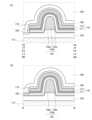
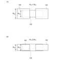
図17(A)、(B)は、本発明の一態様のトランジスタ101の上面図および断面図で
ある。図17(A)に示す一点鎖線B1-B2方向の断面が図17(B)に相当する。ま
た、図17(A)に示す一点鎖線B3-B4方向の断面が図23(A)に相当する。また
、一点鎖線B1-B2方向をチャネル長方向、一点鎖線B3-B4方向をチャネル幅方向
と呼称する場合がある。17A and 17B are a top view and a cross-sectional view of a
トランジスタ101は、基板115と接する絶縁層120と、絶縁層120と接する酸化
物半導体層130と、酸化物半導体層130と電気的に接続する導電層140および導電
層150と、酸化物半導体層130、導電層140および導電層150と接する絶縁層1
60と、絶縁層160と接する導電層170と、導電層140、導電層150、絶縁層1
60および導電層170と接する絶縁層175と、絶縁層175と接する絶縁層180と
、を有する。また、必要に応じて絶縁層180に接する絶縁層190(平坦化膜)などを
有していてもよい。The
60, a
60 and an insulating
ここで、導電層140はソース電極層、導電層150はドレイン電極層、絶縁層160は
ゲート絶縁膜、導電層170はゲート電極層としてそれぞれ機能することができる。Here, the
また、図17(B)に示す領域231はソース領域、領域232はドレイン領域、領域2
33はチャネル形成領域として機能することができる。領域231および領域232は導
電層140および導電層150とそれぞれ接しており、導電層140および導電層150
として酸素と結合しやすい導電材料を用いれば領域231および領域232を低抵抗化す
ることができる。In addition, a
The
If a conductive material that easily bonds with oxygen is used as the insulating
具体的には、酸化物半導体層130と導電層140および導電層150とが接することで
酸化物半導体層130内に酸素欠損が生じ、当該酸素欠損と酸化物半導体層130内に残
留または外部から拡散する水素との相互作用により、領域231および領域232は低抵
抗のn型となる。Specifically, oxygen vacancies are generated in the
なお、トランジスタの「ソース」や「ドレイン」の機能は、異なる極性のトランジスタを
採用する場合や、回路動作において電流の方向が変化する場合などには入れ替わることが
ある。このため、本明細書においては、「ソース」や「ドレイン」という用語は、入れ替
えて用いることができるものとする。また、「電極層」は、「配線」と言い換えることも
できる。Note that the functions of the "source" and "drain" of a transistor may be interchanged when transistors of different polarity are used or when the direction of current changes during circuit operation. For this reason, in this specification, the terms "source" and "drain" may be used interchangeably. In addition, an "electrode layer" may be referred to as a "wiring."
また、導電層170は、導電層171および導電層172の二層で形成される例を図示し
ているが、一層または三層以上の積層であってもよい。当該構成は本実施の形態で説明す
る他のトランジスタにも適用できる。Although the
また、導電層140および導電層150は単層で形成される例を図示しているが、二層以
上の積層であってもよい。当該構成は本実施の形態で説明する他のトランジスタにも適用
できる。Although an example in which the
また、本発明の一態様のトランジスタは、図18(A)、(B)に示す構成であってもよ
い。図18(A)はトランジスタ102の上面図であり、図18(A)に示す一点鎖線C
1-C2方向の断面が図18(B)に相当する。また、図18(A)に示す一点鎖線C3
-C4方向の断面は、図23(B)に相当する。また、一点鎖線C1-C2方向をチャネ
ル長方向、一点鎖線C3-C4方向をチャネル幅方向と呼称する場合がある。The transistor of one embodiment of the present invention may have a structure illustrated in FIGS. 18A and 18B. FIG. 18A is a top view of the
The cross section in the 1-C2 direction corresponds to FIG. 18(B). Also, the dashed line C3 shown in FIG.
The cross section in the -C4 direction corresponds to Fig. 23(B) In addition, the direction of the dashed dotted line C1-C2 may be called the channel length direction, and the direction of the dashed dotted line C3-C4 may be called the channel width direction.
トランジスタ102は、ゲート絶縁膜として作用する絶縁層160の端部とゲート電極層
として作用する導電層170の端部とを一致させない点を除き、トランジスタ101と同
様の構成を有する。トランジスタ102の構造は、導電層140および導電層150が絶
縁層160で広く覆われているため、導電層140および導電層150と導電層170と
の間の抵抗が高く、ゲートリーク電流の少ない特徴を有している。The
トランジスタ101およびトランジスタ102は、導電層170と導電層140および導
電層150が重なる領域を有するトップゲート構造である。当該領域のチャネル長方向の
幅は、寄生容量を小さくするために3nm以上300nm未満とすることが好ましい。一
方で、酸化物半導体層130にオフセット領域が形成されないため、オン電流の高いトラ
ンジスタを形成しやすい。The
また、本発明の一態様のトランジスタは、図19(A)、(B)に示す構成であってもよ
い。図19(A)はトランジスタ103の上面図であり、図19(A)に示す一点鎖線D
1-D2方向の断面が図19(B)に相当する。また、図19(A)に示す一点鎖線D3
-D4方向の断面は、図23(A)に相当する。また、一点鎖線D1-D2方向をチャネ
ル長方向、一点鎖線D3-D4方向をチャネル幅方向と呼称する場合がある。19A and 19B. FIG. 19A is a top view of a
The cross section in the 1-D2 direction corresponds to FIG. 19(B).
The cross section in the -D4 direction corresponds to Fig. 23(A) In addition, the direction of the dashed dotted line D1-D2 may be called the channel length direction, and the direction of the dashed dotted line D3-D4 may be called the channel width direction.
トランジスタ103は、基板115と接する絶縁層120と、絶縁層120と接する酸化
物半導体層130と、酸化物半導体層130と接する絶縁層160と、絶縁層160と接
する導電層170と、酸化物半導体層130、絶縁層160および導電層170を覆う絶
縁層175と、絶縁層175と接する絶縁層180と、絶縁層175および絶縁層180
に設けられた開口部を通じて酸化物半導体層130と電気的に接続する導電層140およ
び導電層150を有する。また、必要に応じて絶縁層180、導電層140および導電層
150に接する絶縁層190(平坦化膜)などを有していてもよい。The
The insulating
ここで、導電層140はソース電極層、導電層150はドレイン電極層、絶縁層160は
ゲート絶縁膜、導電層170はゲート電極層としてそれぞれ機能することができる。Here, the
また、図19(B)に示す領域231はソース領域、領域232はドレイン領域、領域2
33はチャネル形成領域として機能することができる。領域231および領域232は絶
縁層175と接しており、例えば絶縁層175として水素を含む絶縁材料を用いれば領域
231および領域232を低抵抗化することができる。In addition, a
The region 33 can function as a channel formation region. The
具体的には、絶縁層175を形成するまでの工程により領域231および領域232に生
じる酸素欠損と、絶縁層175から領域231および領域232に拡散する水素との相互
作用により、領域231および領域232は低抵抗のn型となる。なお、水素を含む絶縁
材料としては、例えば窒化シリコン膜や窒化アルミニウム膜などを用いることができる。Specifically, the
また、本発明の一態様のトランジスタは、図20(A)、(B)に示す構成であってもよ
い。図20(A)はトランジスタ104の上面図であり、図20(A)に示す一点鎖線E
1-E2方向の断面が図20(B)に相当する。また、図20(A)に示す一点鎖線E3
-E4方向の断面は、図23(A)に相当する。また、一点鎖線E1-E2方向をチャネ
ル長方向、一点鎖線E3-E4方向をチャネル幅方向と呼称する場合がある。20A and 20B. FIG. 20A is a top view of a
The cross section in the 1-E2 direction corresponds to FIG. 20(B). Also, the dashed line E3 shown in FIG.
The cross section in the -E4 direction corresponds to Fig. 23(A) In addition, the direction of the dashed dotted line E1-E2 may be called the channel length direction, and the direction of the dashed dotted line E3-E4 may be called the channel width direction.
トランジスタ104は、導電層140および導電層150が酸化物半導体層130の端部
を覆うように接している点を除き、トランジスタ103と同様の構成を有する。The
また、図20(B)に示す領域331および領域334はソース領域、領域332および
領域335はドレイン領域、領域333はチャネル形成領域として機能することができる
。領域331および領域332はトランジスタ101における領域231および領域23
2と同様に低抵抗化することができる。また、領域334および領域335はトランジス
タ103における領域231および領域232と同様に低抵抗化することができる。なお
、チャネル長方向における領域334および領域335の長さが100nm以下、好まし
くは50nm以下の場合には、ゲート電界の寄与によりオン電流は大きく低下しないため
、上述したような低抵抗化を行わない構成とすることもできる。20B can function as a source region,
2. The resistance of the
トランジスタ103およびトランジスタ104は、導電層170と導電層140および導
電層150が重なる領域を有さないセルフアライン構造である。セルフアライン構造のト
ランジスタはゲート電極層とソース電極層およびドレイン電極層間の寄生容量が極めて小
さいため、高速動作用途に適している。The
また、本発明の一態様のトランジスタは、図21(A)、(B)に示す構成であってもよ
い。図21(A)はトランジスタ105の上面図であり、図21(A)に示す一点鎖線F
1-F2方向の断面が図21(B)に相当する。また、図21(A)に示す一点鎖線F3
-F4方向の断面は、図23(A)に相当。また、一点鎖線F1-F2方向をチャネル長
方向、一点鎖線F3-F4方向をチャネル幅方向と呼称する場合がある。The transistor of one embodiment of the present invention may have a structure illustrated in FIGS. 21A and 21B. FIG. 21A is a top view of the
The cross section in the 1-F2 direction corresponds to FIG. 21(B). Also, the dashed line F3 shown in FIG.
The cross section in the -F4 direction corresponds to Fig. 23(A). The direction of the dashed dotted line F1-F2 may be called the channel length direction, and the direction of the dashed dotted line F3-F4 may be called the channel width direction.
トランジスタ105は、基板115と接する絶縁層120と、絶縁層120と接する酸化
物半導体層130と、酸化物半導体層130と電気的に接続する導電層141および導電
層151と、酸化物半導体層130、導電層141、導電層151と接する絶縁層160
と、絶縁層160と接する導電層170と、酸化物半導体層130、導電層141、導電
層151、絶縁層160および導電層170と接する絶縁層175と、絶縁層175と接
する絶縁層180と、絶縁層175および絶縁層180に設けられた開口部を通じて導電
層141および導電層151とそれぞれ電気的に接続する導電層142および導電層15
2を有する。また、必要に応じて絶縁層180、導電層142および導電層152に接す
る絶縁層190(平坦化膜)などを有していてもよい。The
a
2. If necessary, an insulating
ここで、導電層141および導電層151は、酸化物半導体層130の上面と接し、側面
には接しない構成となっている。Here, the
トランジスタ105は、導電層141および導電層151を有する点、絶縁層175およ
び絶縁層180に設けられた開口部を有する点、ならびに当該開口部を通じて導電層14
1および導電層151とそれぞれ電気的に接続する導電層142および導電層152を有
する点を除き、トランジスタ101と同様の構成を有する。導電層140(導電層141
および導電層142)はソース電極層として作用させることができ、導電層150(導電
層151および導電層152)はドレイン電極層として作用させることができる。The
The
and the conductive layer 142) can serve as a source electrode layer, and the conductive layer 150 (the
また、本発明の一態様のトランジスタは、図22(A)、(B)に示す構成であってもよ
い。図22(A)はトランジスタ106の上面図であり、図22(A)に示す一点鎖線G
1-G2方向の断面が図22(B)に相当する。また、図22(A)に示す一点鎖線G3
-G4方向の断面は、図23(A)に相当する。また、一点鎖線G1-G2方向をチャネ
ル長方向、一点鎖線G3-G4方向をチャネル幅方向と呼称する場合がある。The transistor of one embodiment of the present invention may have a structure illustrated in FIGS. 22A and 22B. FIG. 22A is a top view of the
The cross section in the 1-G2 direction corresponds to FIG. 22(B).
The cross section in the -G4 direction corresponds to Fig. 23(A) In addition, the direction of the dashed dotted line G1-G2 may be called the channel length direction, and the direction of the dashed dotted line G3-G4 may be called the channel width direction.
トランジスタ106は、基板115と接する絶縁層120と、絶縁層120と接する酸化
物半導体層130と、酸化物半導体層130と電気的に接続する導電層141および導電
層151と、酸化物半導体層130と接する絶縁層160と、絶縁層160と接する導電
層170と、絶縁層120、酸化物半導体層130、導電層141、導電層151、絶縁
層160、導電層170と接する絶縁層175と、絶縁層175と接する絶縁層180と
、絶縁層175および絶縁層180に設けられた開口部を通じて導電層141および導電
層151とそれぞれ電気的に接続する導電層142および導電層152を有する。また、
必要に応じて絶縁層180、導電層142および導電層152に接する絶縁層190(平
坦化膜)などを有していてもよい。The
If necessary, an insulating
ここで、導電層141および導電層151は、酸化物半導体層130の上面と接し、側面
には接しない構成となっている。Here, the
トランジスタ106は、導電層141および導電層151を有する点を除き、トランジス
タ103と同様の構成を有する。導電層140(導電層141および導電層142)はソ
ース電極層として作用させることができ、導電層150(導電層151および導電層15
2)はドレイン電極層として作用させることができる。The
2) can act as a drain electrode layer.
トランジスタ105およびトランジスタ106の構成では、導電層140および導電層1
50が絶縁層120と接しない構成であるため、絶縁層120中の酸素が導電層140お
よび導電層150に奪われにくくなり、絶縁層120から酸化物半導体層130中への酸
素の供給を容易とすることができる。In the configurations of the
Since the insulating
なお、トランジスタ103における領域231および領域232、トランジスタ104お
よびトランジスタ106における領域334および領域335には、酸素欠損を形成し導
電率を高めるための不純物を添加してもよい。酸化物半導体層に酸素欠損を形成する不純
物としては、例えば、リン、砒素、アンチモン、ホウ素、アルミニウム、シリコン、窒素
、ヘリウム、ネオン、アルゴン、クリプトン、キセノン、インジウム、フッ素、塩素、チ
タン、亜鉛、および炭素のいずれかから選択される一つ以上を用いることができる。当該
不純物の添加方法としては、プラズマ処理法、イオン注入法、イオンドーピング法、プラ
ズマイマージョンイオンインプランテーション法などを用いることができる。Note that impurities for forming oxygen vacancies and increasing electrical conductivity may be added to the
不純物元素として、上記元素が酸化物半導体層に添加されると、酸化物半導体層中の金属
元素および酸素の結合が切断され、酸素欠損が形成される。酸化物半導体層に含まれる酸
素欠損と酸化物半導体層中に残存または後から添加される水素の相互作用により、酸化物
半導体層の導電率を高くすることができる。When the above-mentioned element is added to the oxide semiconductor layer as an impurity element, a bond between a metal element and oxygen in the oxide semiconductor layer is cut, and oxygen vacancies are formed. The oxygen vacancies in the oxide semiconductor layer interact with hydrogen remaining in the oxide semiconductor layer or added later, thereby increasing the electrical conductivity of the oxide semiconductor layer.
なお、不純物元素の添加により酸素欠損が形成された酸化物半導体に水素を添加すると、
酸素欠損サイトに水素が入り伝導帯近傍にドナー準位が形成される。その結果、酸化物導
電体を形成することができる。なお、ここでは、導電体化された酸化物半導体を酸化物導
電体という。When hydrogen is added to an oxide semiconductor in which oxygen vacancies are formed by the addition of an impurity element,
Hydrogen enters the oxygen vacancy sites and a donor level is formed near the conduction band. As a result, an oxide conductor can be formed. Note that an oxide semiconductor that has been made into a conductor is referred to as an oxide conductor here.
酸化物導電体は、縮退半導体であり、伝導帯端とフェルミ準位とが一致または略一致して
いると推定される。このため、酸化物導電体層とソース電極層およびドレイン電極層とし
て機能する導電層との接触はオーミック接触であり、酸化物導電体層とソース電極層およ
びドレイン電極層として機能する導電層との接触抵抗を低減することができる。The oxide conductor is a degenerate semiconductor, and it is presumed that the conduction band edge and the Fermi level are coincident or approximately coincident with each other. Therefore, the contact between the oxide conductor layer and the conductive layer functioning as the source electrode layer and the drain electrode layer is ohmic contact, and the contact resistance between the oxide conductor layer and the conductive layer functioning as the source electrode layer and the drain electrode layer can be reduced.
また、本発明の一態様のトランジスタは、図24(A)、(B)、(C)および図25(
A)、(B)、(C)に示すチャネル長方向の断面図、ならびに図26(A)、(B)に
示すチャネル幅方向の断面図のように、酸化物半導体層130と基板115との間に導電
層173を備えていてもよい。当該導電層173を第2のゲート電極層(バックゲート)
として用いることで、更なるオン電流の増加や、しきい値電圧の制御を行うことができる
。なお、図24(A)、(B)、(C)および図25(A)、(B)、(C)に示す断面
図において、導電層173の幅を酸化物半導体層130よりも短くしてもよい。さらに、
導電層173の幅を導電層170の幅よりも短くしてもよい。In addition, the transistor of one embodiment of the present invention is shown in FIG.
As shown in the cross-sectional views in the channel length direction shown in FIGS. 26A, 26B, and 26C and the cross-sectional views in the channel width direction shown in FIGS. 26A and 26B, a
25A , 25B, and 25C , the width of the
The width of the
オン電流を増加させるには、例えば、導電層170と導電層173を同電位とし、ダブル
ゲートトランジスタとして駆動させればよい。また、しきい値電圧の制御を行うには、導
電層170とは異なる定電位を導電層173に供給すればよい。導電層170と導電層1
73を同電位とするには、例えば、図26(B)に示すように、導電層170と導電層1
73とをコンタクトホールを介して電気的に接続すればよい。In order to increase the on-current, for example, the
To make the
73 may be electrically connected via a contact hole.
また、図17乃至図22におけるトランジスタ101乃至トランジスタ106では、酸化
物半導体層130が単層である例を図示したが、酸化物半導体層130は積層であっても
よい。トランジスタ101乃至トランジスタ106の酸化物半導体層130は、図27ま
たは図28に示す酸化物半導体層130と入れ替えることができる。17 to 22 illustrate an example in which the
図27(A)、(B)、(C)は、二層構造である酸化物半導体層130の上面図および
断面図である。図27(A)に示す一点鎖線A1-A2方向の断面が図27(B)に相当
する。また、図27(A)に示す一点鎖線A3-A4方向の断面が図27(C)に相当す
る。27A, 27B, and 27C are a top view and a cross-sectional view of the
また、図28(A)、(B)、(C)は、三層構造である酸化物半導体層130の上面図
および断面図である。図28(A)に示す一点鎖線A1-A2方向の断面が図28(B)
に相当する。また、図28(A)に示す一点鎖線A3-A4方向の断面が図28(C)に
相当する。28A, 28B, and 28C are a top view and a cross-sectional view of an
28(A) corresponds to FIG. 28(C).
酸化物半導体層130a、酸化物半導体層130b、酸化物半導体層130cには、それ
ぞれ組成の異なる酸化物半導体層などを用いることができる。The
また、本発明の一態様のトランジスタは、図29(A)、(B)に示す構成であってもよ
い。図29(A)はトランジスタ107の上面図であり、図29(A)に示す一点鎖線H
1-H2方向の断面が図29(B)に相当する。また、図29(A)に示す一点鎖線H3
-H4方向の断面が図35(A)に相当する。また、一点鎖線H1-H2方向をチャネル
長方向、一点鎖線H3-H4方向をチャネル幅方向と呼称する場合がある。29A is a top view of the
The cross section in the 1-H2 direction corresponds to FIG. 29(B).
The cross section in the -H4 direction corresponds to Fig. 35(A). The direction of the dashed dotted line H1-H2 may be called the channel length direction, and the direction of the dashed dotted line H3-H4 may be called the channel width direction.
トランジスタ107は、基板115と接する絶縁層120と、絶縁層120と接する酸化
物半導体層130aおよび酸化物半導体層130bからなる積層と、当該積層と電気的に
接続する導電層140および導電層150と、当該積層、導電層140および導電層15
0と接する酸化物半導体層130cと、酸化物半導体層130cと接する絶縁層160と
、絶縁層160と接する導電層170と、導電層140、導電層150、酸化物半導体層
130c、絶縁層160および導電層170と接する絶縁層175と、絶縁層175と接
する絶縁層180と、を有する。また、必要に応じて絶縁層180に接する絶縁層190
(平坦化膜)などを有していてもよい。The
1, an
(planarization film) or the like.
トランジスタ107は、領域231および領域232において酸化物半導体層130が二
層(酸化物半導体層130a、酸化物半導体層130b)である点、領域233において
酸化物半導体層130が三層(酸化物半導体層130a、酸化物半導体層130b、酸化
物半導体層130c)である点、および導電層140および導電層150と絶縁層160
との間に酸化物半導体層の一部(酸化物半導体層130c)が介在している点を除き、ト
ランジスタ101と同様の構成を有する。The
The
また、本発明の一態様のトランジスタは、図30(A)、(B)に示す構成であってもよ
い。図30(A)はトランジスタ108の上面図であり、図30(A)に示す一点鎖線I
1-I2方向の断面が図30(B)に相当する。また、図30(A)に示す一点鎖線I3
-I4方向の断面が図35(B)に相当する。また、一点鎖線I1-I2方向をチャネル
長方向、一点鎖線I3-I4方向をチャネル幅方向と呼称する場合がある。The transistor of one embodiment of the present invention may have a structure illustrated in FIGS. 30A and 30B. FIG. 30A is a top view of the
The cross section in the 1-I2 direction corresponds to FIG. 30(B).
The cross section in the -I4 direction corresponds to Fig. 35(B) In addition, the direction of the dashed dotted line I1-I2 may be called the channel length direction, and the direction of the dashed dotted line I3-I4 may be called the channel width direction.
トランジスタ108は、絶縁層160および酸化物半導体層130cの端部が導電層17
0の端部と一致しない点がトランジスタ107と異なる。In the
It differs from
また、本発明の一態様のトランジスタは、図31(A)、(B)に示す構成であってもよ
い。図31(A)はトランジスタ109の上面図であり、図31(A)に示す一点鎖線J
1-J2方向の断面が図31(B)に相当する。また、図31(A)に示す一点鎖線J3
-J4方向の断面が図35(A)に相当する。また、一点鎖線J1-J2方向をチャネル
長方向、一点鎖線J3-J4方向をチャネル幅方向と呼称する場合がある。The transistor of one embodiment of the present invention may have a structure illustrated in FIGS. 31A and 31B. FIG. 31A is a top view of a
The cross section in the 1-J2 direction corresponds to FIG. 31(B).
The cross section in the -J4 direction corresponds to Fig. 35(A). The direction of the dashed dotted line J1-J2 may be called the channel length direction, and the direction of the dashed dotted line J3-J4 may be called the channel width direction.
トランジスタ109は、基板115と接する絶縁層120と、絶縁層120と接する酸化
物半導体層130aおよび酸化物半導体層130bからなる積層と、当該積層と接する酸
化物半導体層130cと、酸化物半導体層130cと接する絶縁層160と、絶縁層16
0と接する導電層170と、当該積層、酸化物半導体層130c、絶縁層160および導
電層170を覆う絶縁層175と、絶縁層175と接する絶縁層180と、絶縁層175
および絶縁層180に設けられた開口部を通じて当該積層と電気的に接続する導電層14
0および導電層150を有する。また、必要に応じて絶縁層180、導電層140および
導電層150に接する絶縁層190(平坦化膜)などを有していてもよい。The
1, an insulating
and a
1 and a
トランジスタ109は、領域231および領域232において酸化物半導体層130が二
層(酸化物半導体層130a、酸化物半導体層130b)である点、領域233において
酸化物半導体層130が三層(酸化物半導体層130a、酸化物半導体層130b、酸化
物半導体層130c)である点を除き、トランジスタ103と同様の構成を有する。The
また、本発明の一態様のトランジスタは、図32(A)、(B)に示す構成であってもよ
い。図32(A)はトランジスタ110の上面図であり、図32(A)に示す一点鎖線K
1-K2方向の断面が図32(B)に相当する。また、図32(A)に示す一点鎖線K3
-K4方向の断面が図35(A)に相当する。また、一点鎖線K1-K2方向をチャネル
長方向、一点鎖線K3-K4方向をチャネル幅方向と呼称する場合がある。The transistor of one embodiment of the present invention may have a structure illustrated in FIGS. 32A and 32B. FIG. 32A is a top view of the
The cross section in the 1-K2 direction corresponds to FIG. 32(B).
The cross section in the -K4 direction corresponds to Fig. 35(A). The direction of the dashed dotted line K1-K2 may be called the channel length direction, and the direction of the dashed dotted line K3-K4 may be called the channel width direction.
トランジスタ110は、領域331および領域332において酸化物半導体層130が二
層(酸化物半導体層130a、酸化物半導体層130b)である点、領域333において
酸化物半導体層130が三層(酸化物半導体層130a、酸化物半導体層130b、酸化
物半導体層130c)である点を除き、トランジスタ104と同様の構成を有する。The
また、本発明の一態様のトランジスタは、図33(A)、(B)に示す構成であってもよ
い。図33(A)はトランジスタ111の上面図であり、図33(A)に示す一点鎖線L
1-L2方向の断面が図33(B)に相当する。また、図33(A)に示す一点鎖線L3
-L4方向の断面が図35(A)に相当する。また、一点鎖線L1-L2方向をチャネル
長方向、一点鎖線L3-L4方向をチャネル幅方向と呼称する場合がある。The transistor of one embodiment of the present invention may have a structure illustrated in FIGS. 33A and 33B. FIG. 33A is a top view of the
The cross section in the 1-L2 direction corresponds to FIG. 33(B).
The cross section in the -L4 direction corresponds to Fig. 35(A). The direction of the dashed dotted line L1-L2 may be called the channel length direction, and the direction of the dashed dotted line L3-L4 may be called the channel width direction.
トランジスタ111は、基板115と接する絶縁層120と、絶縁層120と接する酸化
物半導体層130aおよび酸化物半導体層130bからなる積層と、当該積層と電気的に
接続する導電層141および導電層151と、当該積層、導電層141および導電層15
1と接する酸化物半導体層130cと、酸化物半導体層130cと接する絶縁層160と
、絶縁層160と接する導電層170と、当該積層、導電層141、導電層151、酸化
物半導体層130c、絶縁層160および導電層170と接する絶縁層175と、絶縁層
175と接する絶縁層180と、絶縁層175および絶縁層180に設けられた開口部を
通じて導電層141および導電層151とそれぞれ電気的に接続する導電層142および
導電層152を有する。また、必要に応じて絶縁層180、導電層142および導電層1
52に接する絶縁層190(平坦化膜)などを有していてもよい。The
The insulating
52, and the like.
トランジスタ111は、領域231および領域232において酸化物半導体層130が二
層(酸化物半導体層130a、酸化物半導体層130b)である点、領域233において
酸化物半導体層130が三層(酸化物半導体層130a、酸化物半導体層130b、酸化
物半導体層130c)である点、および導電層141および導電層151と絶縁層160
との間に酸化物半導体層の一部(酸化物半導体層130c)が介在している点を除き、ト
ランジスタ105と同様の構成を有する。The
The
また、本発明の一態様のトランジスタは、図34(A)、(B)に示す構成であってもよ
い。図34(A)はトランジスタ112の上面図であり、図34(A)に示す一点鎖線M
1-M2方向の断面が図34(B)に相当する。また、図34(A)に示す一点鎖線M3
-M4方向の断面が図35(A)に相当する。また、一点鎖線M1-M2方向をチャネル
長方向、一点鎖線M3-M4方向をチャネル幅方向と呼称する場合がある。The transistor of one embodiment of the present invention may have a structure illustrated in FIGS. 34A and 34B. FIG. 34A is a top view of the
The cross section in the 1-M2 direction corresponds to FIG. 34(B). Also, the dashed line M3 shown in FIG.
The cross section in the -M4 direction corresponds to Fig. 35(A). The direction of the dashed dotted line M1-M2 may be called the channel length direction, and the direction of the dashed dotted line M3-M4 may be called the channel width direction.
トランジスタ112は、領域331、領域332、領域334および領域335において
酸化物半導体層130が二層(酸化物半導体層130a、酸化物半導体層130b)であ
る点、領域333において酸化物半導体層130が三層(酸化物半導体層130a、酸化
物半導体層130b、酸化物半導体層130c)である点を除き、トランジスタ106と
同様の構成を有する。The
また、本発明の一態様のトランジスタは、図36(A)、(B)、(C)および図37(
A)、(B)、(C)に示すチャネル長方向の断面図、ならびに図38(A)、(B)に
示すチャネル幅方向の断面図のように、酸化物半導体層130と基板115との間に導電
層173を備えていてもよい。当該導電層を第2のゲート電極層(バックゲート)として
用いることで、更なるオン電流の増加や、しきい値電圧の制御を行うことができる。なお
、図36(A)、(B)、(C)および図37(A)、(B)、(C)に示す断面図にお
いて、導電層173の幅を酸化物半導体層130よりも短くしてもよい。さらに、導電層
173の幅を導電層170の幅よりも短くしてもよい。In addition, the transistor of one embodiment of the present invention is shown in FIG.
As shown in the cross-sectional views in the channel length direction shown in FIGS. 3A, 3B, and 3C and the cross-sectional views in the channel width direction shown in FIGS. 38A and 38B, a
また、本発明の一態様のトランジスタにおける導電層140(ソース電極層)および導電
層150(ドレイン電極層)は、図39(A)、(B)に示す上面図のような構成とする
ことができる。なお、図39(A)、(B)では、酸化物半導体層130、導電層140
および導電層150のみを図示している。図39(A)に示すように、導電層140およ
び導電層150の幅(WSD)は、酸化物半導体層の幅(WOS)よりも長く形成されて
いてもよい。また、図39(B)に示すように、WSDはWOSよりも短く形成されてい
てもよい。WOS≧WSD(WSDはWOS以下)とすることで、ゲート電界が酸化物半
導体層130全体にかかりやすくなり、トランジスタの電気特性を向上させることができ
る。The conductive layer 140 (source electrode layer) and the conductive layer 150 (drain electrode layer) in the transistor of one embodiment of the present invention can have a structure as shown in the top views in FIGS.
Only the
本発明の一態様のトランジスタ(トランジスタ101乃至トランジスタ112)では、い
ずれの構成においても、ゲート電極層である導電層170は、ゲート絶縁膜である絶縁層
160を介して酸化物半導体層130のチャネル幅方向を電気的に取り囲み、オン電流が
高められる。このようなトランジスタの構造を、surrounded channel
(s-channel)構造とよぶ。In any of the transistors of one embodiment of the present invention (the
This is called an (s-channel) structure.
また、酸化物半導体層130bおよび酸化物半導体層130cを有するトランジスタ、な
らびに酸化物半導体層130a、酸化物半導体層130bおよび酸化物半導体層130c
を有するトランジスタにおいては、酸化物半導体層130を構成する二層または三層の材
料を適切に選択することで酸化物半導体層130bに電流を流すことができる。酸化物半
導体層130bに電流が流れることで、界面散乱の影響を受けにくく、高いオン電流を得
ることができる。なお、酸化物半導体層130bを厚くすると、オン電流を向上させるこ
とができる。例えば、酸化物半導体層130bの膜厚を100nm乃至200nmとして
もよい。In addition, a transistor including the
In a transistor having the above structure, a current can flow through the
以上の構成のトランジスタを用いることにより、半導体装置に良好な電気特性を付与する
ことができる。By using a transistor having the above structure, a semiconductor device can have favorable electrical characteristics.
なお、本明細書において、チャネル長とは、例えば、トランジスタの上面図において、半
導体(またはトランジスタがオン状態のときに半導体の中で電流の流れる部分)とゲート
電極とが重なる領域、またはチャネルが形成される領域における、ソース(ソース領域ま
たはソース電極)とドレイン(ドレイン領域またはドレイン電極)との間の距離をいう。
なお、一つのトランジスタにおいて、チャネル長が全ての領域で同じ値をとるとは限らな
い。即ち、一つのトランジスタのチャネル長は、一つの値に定まらない場合がある。その
ため、本明細書では、チャネル長は、チャネルの形成される領域における、いずれか一の
値、最大値、最小値または平均値とする。In this specification, the channel length refers to, for example, the distance between the source (source region or source electrode) and the drain (drain region or drain electrode) in a region where a channel is formed, or in a region where a semiconductor (or a portion in the semiconductor through which current flows when the transistor is on) and a gate electrode overlap in a top view of a transistor.
Note that the channel length of one transistor does not necessarily have the same value in all regions. That is, the channel length of one transistor may not be determined to one value. Therefore, in this specification, the channel length is defined as any one value, maximum value, minimum value, or average value in the region where the channel is formed.
また、チャネル幅とは、例えば、半導体(またはトランジスタがオン状態のときに半導体
の中で電流の流れる部分)とゲート電極とが重なる領域、またはチャネルが形成される領
域における、ソースとドレインとが向かい合っている部分の長さをいう。なお、一つのト
ランジスタにおいて、チャネル幅がすべての領域で同じ値をとるとは限らない。即ち、一
つのトランジスタのチャネル幅は、一つの値に定まらない場合がある。そのため、本明細
書では、チャネル幅は、チャネルの形成される領域における、いずれか一の値、最大値、
最小値または平均値とする。The channel width refers to, for example, the length of the region where the semiconductor (or the portion in the semiconductor through which current flows when the transistor is on) and the gate electrode overlap, or the length of the portion where the source and drain face each other in the region where the channel is formed. Note that the channel width of one transistor does not necessarily have the same value in all regions. That is, the channel width of one transistor may not be determined to a single value. For this reason, in this specification, the channel width refers to any one value, maximum value, or the length of the region where the channel is formed.
The minimum or average value.
なお、トランジスタの構造によっては、実際にチャネルの形成される領域におけるチャネ
ル幅(以下、実効的なチャネル幅と呼ぶ。)と、トランジスタの上面図において示される
チャネル幅(以下、見かけ上のチャネル幅と呼ぶ。)と、が異なる場合がある。例えば、
ゲート電極が半導体の側面を覆う場合、実効的なチャネル幅が、見かけ上のチャネル幅よ
りも大きくなり、その影響が無視できなくなる場合がある。例えば、微細かつゲート電極
が半導体の側面を覆うトランジスタでは、半導体の上面に形成されるチャネル領域の割合
に対して、半導体の側面に形成されるチャネル領域の割合が大きくなる場合がある。その
場合は、見かけ上のチャネル幅よりも、実効的なチャネル幅の方が大きくなる。Depending on the structure of a transistor, the channel width in a region where a channel is actually formed (hereinafter referred to as an effective channel width) may differ from the channel width shown in a top view of the transistor (hereinafter referred to as an apparent channel width).
When the gate electrode covers the side surface of the semiconductor, the effective channel width becomes larger than the apparent channel width, and the influence of this may become unnegligible. For example, in a fine transistor in which the gate electrode covers the side surface of the semiconductor, the ratio of the channel region formed on the side surface of the semiconductor may be larger than the ratio of the channel region formed on the top surface of the semiconductor. In this case, the effective channel width becomes larger than the apparent channel width.
このような場合、実効的なチャネル幅の、実測による見積もりが困難となる場合がある。
例えば、設計値から実効的なチャネル幅を見積もるためには、半導体の形状が既知という
仮定が必要である。したがって、半導体の形状が正確にわからない場合には、実効的なチ
ャネル幅を正確に測定することは困難である。In such a case, it may be difficult to estimate the effective channel width through actual measurement.
For example, in order to estimate the effective channel width from the design value, it is necessary to assume that the shape of the semiconductor is known. Therefore, if the shape of the semiconductor is not precisely known, it is difficult to accurately measure the effective channel width.
そこで、本明細書では、見かけ上のチャネル幅を、「囲い込みチャネル幅(SCW:Su
rrounded Channel Width)」と呼ぶ場合がある。また、本明細書
では、単にチャネル幅と記載した場合には、囲い込みチャネル幅または見かけ上のチャネ
ル幅を指す場合がある。または、本明細書では、単にチャネル幅と記載した場合には、実
効的なチャネル幅を指す場合がある。なお、チャネル長、チャネル幅、実効的なチャネル
幅、見かけ上のチャネル幅、囲い込みチャネル幅などは、断面TEM像を解析することな
どによって、値を決定することができる。Therefore, in this specification, the apparent channel width is defined as the "enclosed channel width (SCW: Su
In this specification, when simply referred to as a channel width, it may refer to a surrounded channel width or an apparent channel width. In this specification, when simply referred to as a channel width, it may refer to an effective channel width. Note that the values of the channel length, channel width, effective channel width, apparent channel width, surrounded channel width, etc. can be determined by analyzing a cross-sectional TEM image, etc.
なお、トランジスタの電界効果移動度や、チャネル幅当たりの電流値などを計算して求め
る場合、囲い込みチャネル幅を用いて計算する場合がある。その場合には、実効的なチャ
ネル幅を用いて計算する場合とは異なる値をとる場合がある。In addition, when calculating the field effect mobility of a transistor, the current value per channel width, and the like, the calculation may be performed using the enclosed channel width. In that case, the calculated value may be different from the value calculated using the effective channel width.
なお、本実施の形態は、本明細書で示す他の実施の形態と適宜組み合わせることができる
。Note that this embodiment mode can be appropriately combined with other embodiment modes described in this specification.
(実施の形態6)
本実施の形態では、実施の形態5に示したトランジスタの構成要素について詳細を説明す
る。(Embodiment 6)
In this embodiment, components of the transistor described in Embodiment 5 will be described in detail.
基板115は、トランジスタおよびフォトダイオードが形成されたシリコン基板、および
当該シリコン基板上に絶縁層、配線、コンタクトプラグとして機能を有する導電体が形成
されたものであり、図1(A)における第1の層1100および第2の層1200に相当
する。シリコン基板にp-ch型のトランジスタを形成する場合、n-型の導電型を有す
るシリコン基板を用いることが好ましい。または、n-型またはi型のシリコン層を有す
るSOI基板であってもよい。また、当該シリコン基板におけるトランジスタを形成する
面の面方位は、(110)面であることが好ましい。(110)面にp-ch型トランジ
スタを形成することで、移動度を高くすることができる。The
絶縁層120は、基板115に含まれる要素からの不純物の拡散を防止する役割を有する
ほか、酸化物半導体層130に酸素を供給する役割を担うことができる。したがって、絶
縁層120は酸素を含む絶縁膜であることが好ましく、化学量論組成よりも多い酸素を含
む絶縁膜であることがより好ましい。例えば、膜の表面温度が100℃以上700℃以下
、好ましくは100℃以上500℃以下の加熱処理で行われるTDS法にて、酸素原子に
換算しての酸素の放出量が1.0×10¹⁹atoms/cm3以上である膜とする。絶
縁層120は、層間絶縁膜としての機能も有し、表面が平坦になるようにCMP(Che
mical Mechanical Polishing)法等で平坦化処理を行っても
よい。The insulating
A planarization process may be performed by a method such as a chemical mechanical polishing method.
例えば、絶縁層120には、酸化アルミニウム、酸化マグネシウム、酸化シリコン、酸化
窒化シリコン、酸化ガリウム、酸化ゲルマニウム、酸化イットリウム、酸化ジルコニウム
、酸化ランタン、酸化ネオジム、酸化ハフニウムおよび酸化タンタルなどの酸化物絶縁膜
、窒化シリコン、窒化酸化シリコン、窒化アルミニウム、窒化酸化アルミニウムなどの窒
化物絶縁膜、またはこれらの混合材料を用いることができる。また、上記材料の積層であ
ってもよい。For example, the insulating
なお、本実施の形態では、トランジスタが有する酸化物半導体層130が酸化物半導体層
130a、酸化物半導体層130bおよび酸化物半導体層130cを絶縁層120側から
順に積んだ三層構造である場合を主として詳細を説明する。Note that in this embodiment, the details will be mainly described assuming that the
なお、酸化物半導体層130が単層の場合は、本実施の形態に示す、酸化物半導体層13
0bに相当する層を用いればよい。Note that in the case where the
0b的层可以使用。 0b layer can be used.
また、酸化物半導体層130が二層の場合は、本実施の形態に示す、酸化物半導体層13
0bに相当する層および酸化物半導体層130cに相当する層を絶縁層120側から順に
積んだ積層を用いればよい。この構成の場合、酸化物半導体層130bと酸化物半導体層
130cとを入れ替えることもできる。In addition, in the case where the
A stack of a layer corresponding to the
また、酸化物半導体層130が四層以上である場合は、例えば、本実施の形態で説明する
三層構造の酸化物半導体層130に対して他の酸化物半導体層を付加する構成とすること
ができる。When the
一例としては、酸化物半導体層130bには、酸化物半導体層130aおよび酸化物半導
体層130cよりも電子親和力(真空準位から伝導帯下端までのエネルギー)が大きい酸
化物半導体を用いる。電子親和力は、真空準位と価電子帯上端とのエネルギー差(イオン
化ポテンシャル)から、伝導帯下端と価電子帯上端とのエネルギー差(エネルギーギャッ
プ)を差し引いた値として求めることができる。For example, the
酸化物半導体層130aおよび酸化物半導体層130cは、酸化物半導体層130bを構
成する金属元素を一種以上含み、例えば、伝導帯下端のエネルギーが酸化物半導体層13
0bよりも、0.05eV、0.07eV、0.1eV、0.15eVのいずれか以上で
あって、2eV、1eV、0.5eV、0.4eVのいずれか以下の範囲で真空準位に近
い酸化物半導体で形成することが好ましい。The
It is preferable to use an oxide semiconductor having a vacuum level closer to 0.05 eV, 0.07 eV, 0.1 eV, or 0.15 eV or more and 2 eV, 1 eV, 0.5 eV, or 0.4 eV or less than 0b.
このような構造において、導電層170に電界を印加すると、酸化物半導体層130のう
ち、伝導帯下端のエネルギーが最も小さい酸化物半導体層130bにチャネルが形成され
る。In such a structure, when an electric field is applied to the
また、酸化物半導体層130aは、酸化物半導体層130bを構成する金属元素を一種以
上含んで構成されるため、酸化物半導体層130bと絶縁層120が接した場合の界面と
比較して、酸化物半導体層130bと酸化物半導体層130aとの界面には界面準位が形
成されにくくなる。該界面準位はチャネルを形成することがあるため、トランジスタのし
きい値電圧が変動することがある。したがって、酸化物半導体層130aを設けることに
より、トランジスタのしきい値電圧などの電気特性のばらつきを低減することができる。
また、当該トランジスタの信頼性を向上させることができる。In addition, since the
In addition, the reliability of the transistor can be improved.
また、酸化物半導体層130cは、酸化物半導体層130bを構成する金属元素を一種以
上含んで構成されるため、酸化物半導体層130bとゲート絶縁膜(絶縁層160)が接
した場合の界面と比較して、酸化物半導体層130bと酸化物半導体層130cとの界面
ではキャリアの散乱が起こりにくくなる。したがって、酸化物半導体層130cを設ける
ことにより、トランジスタの電界効果移動度を高くすることができる。In addition, since the
酸化物半導体層130aおよび酸化物半導体層130cには、例えば、Al、Ti、Ga
、Ge、Y、Zr、Sn、La、CeまたはHfを酸化物半導体層130bよりも高い原
子数比で含む材料を用いることができる。具体的には、当該原子数比を1.5倍以上、好
ましくは2倍以上、さらに好ましくは3倍以上とする。前述の元素は酸素と強く結合する
ため、酸素欠損が酸化物半導体層に生じることを抑制する機能を有する。すなわち、酸化
物半導体層130aおよび酸化物半導体層130cは、酸化物半導体層130bよりも酸
素欠損が生じにくいということができる。The
, Ge, Y, Zr, Sn, La, Ce, or Hf in an atomic ratio higher than that of the
また、酸化物半導体層130a、酸化物半導体層130b、および酸化物半導体層130
cとして用いることのできる酸化物半導体は、少なくともInもしくはZnを含むことが
好ましい。または、InとZnの双方を含むことが好ましい。また、該酸化物半導体を用
いたトランジスタの電気特性のばらつきを減らすため、それらと共に、スタビライザーを
含むことが好ましい。In addition, the
The oxide semiconductor that can be used as c preferably contains at least In or Zn, or preferably contains both In and Zn. In addition, in order to reduce variation in electrical characteristics of a transistor using the oxide semiconductor, the oxide semiconductor preferably contains a stabilizer in addition to the In or Zn.
スタビライザーとしては、Ga、Sn、Hf、Al、またはZr等がある。また、他のス
タビライザーとしては、ランタノイドであるLa、Ce、Pr、Nd、Sm、Eu、Gd
、Tb、Dy、Ho、Er、Tm、Yb、Lu等がある。The stabilizer may be Ga, Sn, Hf, Al, or Zr. Other stabilizers include lanthanides such as La, Ce, Pr, Nd, Sm, Eu, and Gd.
, Tb, Dy, Ho, Er, Tm, Yb, Lu, etc.
例えば、酸化物半導体として、酸化インジウム、酸化スズ、酸化ガリウム、酸化亜鉛、I
n-Zn酸化物、Sn-Zn酸化物、Al-Zn酸化物、Zn-Mg酸化物、Sn-Mg
酸化物、In-Mg酸化物、In-Ga酸化物、In-Ga-Zn酸化物、In-Al-
Zn酸化物、In-Sn-Zn酸化物、Sn-Ga-Zn酸化物、Al-Ga-Zn酸化
物、Sn-Al-Zn酸化物、In-Hf-Zn酸化物、In-La-Zn酸化物、In
-Ce-Zn酸化物、In-Pr-Zn酸化物、In-Nd-Zn酸化物、In-Sm-
Zn酸化物、In-Eu-Zn酸化物、In-Gd-Zn酸化物、In-Tb-Zn酸化
物、In-Dy-Zn酸化物、In-Ho-Zn酸化物、In-Er-Zn酸化物、In
-Tm-Zn酸化物、In-Yb-Zn酸化物、In-Lu-Zn酸化物、In-Sn-
Ga-Zn酸化物、In-Hf-Ga-Zn酸化物、In-Al-Ga-Zn酸化物、I
n-Sn-Al-Zn酸化物、In-Sn-Hf-Zn酸化物、In-Hf-Al-Zn
酸化物を用いることができる。For example, oxide semiconductors include indium oxide, tin oxide, gallium oxide, zinc oxide, and I
n-Zn oxide, Sn-Zn oxide, Al-Zn oxide, Zn-Mg oxide, Sn-Mg
oxide, In-Mg oxide, In-Ga oxide, In-Ga-Zn oxide, In-Al-
Zn oxide, In-Sn-Zn oxide, Sn-Ga-Zn oxide, Al-Ga-Zn oxide, Sn-Al-Zn oxide, In-Hf-Zn oxide, In-La-Zn oxide, In
-Ce-Zn oxide, In-Pr-Zn oxide, In-Nd-Zn oxide, In-Sm-
Zn oxide, In-Eu-Zn oxide, In-Gd-Zn oxide, In-Tb-Zn oxide, In-Dy-Zn oxide, In-Ho-Zn oxide, In-Er-Zn oxide, In
-Tm-Zn oxide, In-Yb-Zn oxide, In-Lu-Zn oxide, In-Sn-
Ga-Zn oxide, In-Hf-Ga-Zn oxide, In-Al-Ga-Zn oxide, I
n-Sn-Al-Zn oxide, In-Sn-Hf-Zn oxide, In-Hf-Al-Zn
An oxide can be used.
なお、ここで、例えば、In-Ga-Zn酸化物とは、InとGaとZnを主成分として
有する酸化物という意味である。また、InとGaとZn以外の金属元素が入っていても
よい。また、本明細書においては、In-Ga-Zn酸化物で構成した膜をIGZO膜と
も呼ぶ。In addition, for example, In-Ga-Zn oxide means an oxide having In, Ga, and Zn as main components. Metal elements other than In, Ga, and Zn may also be included. In addition, in this specification, a film composed of In-Ga-Zn oxide is also called an IGZO film.
また、InMO3(ZnO)m(m>0、且つ、mは整数でない)で表記される材料を用
いてもよい。なお、Mは、Ga、Y、Zr、La、Ce、またはNdから選ばれた一つの
金属元素または複数の金属元素を示す。また、In2SnO5(ZnO)n(n>0、且
つ、nは整数)で表記される材料を用いてもよい。Also, a material expressed asInMO3 (ZnO)m (m>0 and m is notan integer) may be used. Here, M represents one or more metal elements selected from Ga, Y, Zr, La, Ce, and Nd. Also, a material expressed asIn2SnO5 (ZnO)n (n>0 and n is an integer) may be used.
なお、酸化物半導体層130a、酸化物半導体層130b、酸化物半導体層130cが、
少なくともインジウム、亜鉛およびM(Al、Ti、Ga、Ge、Y、Zr、Sn、La
、CeまたはHf等の金属)を含むIn-M-Zn酸化物であるとき、酸化物半導体層1
30aをIn:M:Zn=x1:y1:z1[原子数比]、酸化物半導体層130bをI
n:M:Zn=x2:y2:z2[原子数比]、酸化物半導体層130cをIn:M:Z
n=x3:y3:z3[原子数比]とすると、y1/x1およびy3/x3がy2/x2
よりも大きくなることが好ましい。y1/x1およびy3/x3はy2/x2よりも1.
5倍以上、好ましくは2倍以上、さらに好ましくは3倍以上とする。このとき、酸化物半
導体層130bにおいて、y2がx2以上であるとトランジスタの電気特性を安定させる
ことができる。ただし、y2がx2の3倍以上になると、トランジスタの電界効果移動度
が低下してしまうため、y2はx2の3倍未満であることが好ましい。The
At least indium, zinc and M (Al, Ti, Ga, Ge, Y, Zr, Sn, La
When the
The oxide semiconductor layer 30a has an atomic ratio of In:M:Zn=x1 :y1 :z1 , and the
The
If n =x3 :y3 :z3 [atomic ratio], theny1 /x1 andy3 /x3 arey2 /x2
It is preferable thaty1 /x1 andy3 /x3 are 1.0 or less thany2 /x2 .
The ratio is set to 5 times or more, preferably 2 times or more, and more preferably 3 times or more. In this case, wheny2 is equal to or greater thanx2 in the
酸化物半導体層130aおよび酸化物半導体層130cにおけるZnおよびOを除いた場
合において、InおよびMの原子数比率は、好ましくはInが50atomic%未満、
Mが50atomic%以上、さらに好ましくはInが25atomic%未満、Mが7
5atomic%以上とする。また、酸化物半導体層130bのZnおよびOを除いての
InおよびMの原子数比率は、好ましくはInが25atomic%以上、Mが75at
omic%未満、さらに好ましくはInが34atomic%以上、Mが66atomi
c%未満とする。In the
M is 50 atomic % or more, more preferably In is less than 25 atomic %, and M is 7
The atomic ratio of In and M excluding Zn and O in the
More preferably, In is 34 atomic % or more and M is 66 atomic % or more.
The content shall be less than c%.
また、酸化物半導体層130bは、酸化物半導体層130aおよび酸化物半導体層130
cよりもインジウムの含有量を多くするとよい。酸化物半導体では主として重金属のs軌
道がキャリア伝導に寄与しており、Inの含有率を多くすることにより、より多くのs軌
道が重なるため、InがMよりも多い酸化物はInがMと同等または少ない酸化物と比較
して移動度が高くなる。そのため、酸化物半導体層130bにインジウムの含有量が多い
酸化物を用いることで、高い電界効果移動度のトランジスタを実現することができる。The
It is preferable that the indium content is higher than that of M. In an oxide semiconductor, s orbitals of heavy metals mainly contribute to carrier conduction, and by increasing the In content, more s orbitals overlap, so that an oxide having more In than M has higher mobility than an oxide having the same or less In than M. Therefore, by using an oxide having a high indium content for the
酸化物半導体層130aの厚さは、3nm以上100nm以下、好ましくは5nm以上5
0nm以下、さらに好ましくは5nm以上25nm以下とする。また、酸化物半導体層1
30bの厚さは、3nm以上200nm以下、好ましくは10nm以上150nm以下、
さらに好ましくは15nm以上100nm以下とする。また、酸化物半導体層130cの
厚さは、1nm以上50nm以下、好ましくは2nm以上30nm以下、さらに好ましく
は3nm以上15nm以下とする。また、酸化物半導体層130bは、酸化物半導体層1
30aおよび酸化物半導体層130cより厚い方が好ましい。The thickness of the
The thickness of the
The thickness of 30b is 3 nm or more and 200 nm or less, preferably 10 nm or more and 150 nm or less.
The thickness of the
It is preferable that the thickness of the oxide semiconductor layer 30a is larger than that of the
なお、酸化物半導体層をチャネルとするトランジスタに安定した電気特性を付与するため
には、酸化物半導体層中の不純物濃度を低減し、酸化物半導体層を真性(i型)または実
質的に真性にすることが有効である。ここで、実質的に真性とは、酸化物半導体層のキャ
リア密度が、1×10¹⁵/cm3未満であること、1×1013/cm3未満であるこ
と、8×10¹¹/cm3未満であること、あるいは1×108/cm3未満であり、か
つ1×10⁻⁹/cm3以上であることとする。In order to impart stable electrical characteristics to a transistor using an oxide semiconductor layer as a channel, it is effective to reduce the impurity concentration in the oxide semiconductor layer to make the oxide semiconductor layer intrinsic (i-type) or substantially intrinsic. Here, "substantially intrinsic" means that the carrier density of the oxide semiconductor layer is less than 1×10¹⁵ /cm3 , less than 1×10¹³ /cm3 , less than 8×10¹¹ /cm3 , or less than 1×10⁸ /cm3 and 1×10⁻⁹ /cm3 or more.
また、酸化物半導体層において、水素、窒素、炭素、シリコン、および主成分以外の金属
元素は不純物となる。例えば、水素および窒素はドナー準位の形成に寄与し、キャリア密
度を増大させてしまう。また、シリコンは酸化物半導体層中で不純物準位の形成に寄与す
る。当該不純物準位はトラップとなり、トランジスタの電気特性を劣化させることがある
。したがって、酸化物半導体層130a、酸化物半導体層130bおよび酸化物半導体層
130cの層中や、それぞれの界面において不純物濃度を低減させることが好ましい。In the oxide semiconductor layer, hydrogen, nitrogen, carbon, silicon, and metal elements other than the main component become impurities. For example, hydrogen and nitrogen contribute to the formation of donor levels and increase the carrier density. Silicon contributes to the formation of impurity levels in the oxide semiconductor layer. The impurity levels become traps and may deteriorate the electrical characteristics of the transistor. Therefore, it is preferable to reduce the impurity concentrations in the
酸化物半導体層を真性または実質的に真性とするためには、SIMS(Secondar
y Ion Mass Spectrometry)分析で見積もられるシリコン濃度が
1×10¹⁹atoms/cm3未満、好ましくは5×1018atoms/cm3未満
、さらに好ましくは1×10¹⁸atoms/cm3未満となる領域を有するように制御
する。また、水素濃度が、2×10²⁰atoms/cm3以下、好ましくは5×101
9atoms/cm3以下、より好ましくは1×1019atoms/cm3以下、さら
に好ましくは5×10¹⁸atoms/cm3以下になる領域を有するように制御する。
また、窒素濃度は、例えば、酸化物半導体層のある深さにおいて、または、酸化物半導体
層のある領域において、5×10¹⁹atoms/cm3未満、好ましくは5×1018
atoms/cm3以下、より好ましくは1×1018atoms/cm3以下、さらに
好ましくは5×10¹⁷atoms/cm3以下とする。In order to make the oxide semiconductor layer intrinsic or substantially intrinsic, a SIMS (Secondary Induction Measuring System) is used.
The silicon concentration estimated by ion mass spectrometry (Ion Mass Spectrometry) analysisis controlled to have a region where the silicon concentration is less than 1×10¹⁹ atoms/cm3 , preferably less than 5×10¹⁸ atoms/cm3 , and more preferably less than 1×10¹⁸ atoms/cm 3 . The hydrogen concentration is controlled to be 2×10²⁰ atoms/cm3 or less, preferably 5×101
9 atoms/cm3 or less, more preferably 1×10¹⁹ atoms/cm3 or less, and further preferably 5×10¹⁸ atoms/cm3 or less.
The nitrogen concentration is, for example, less than 5×10¹⁹ atoms/cm3 , preferably less than 5×10¹⁸ atoms/cm 3 at a certain depth or in a certain region of the oxide semiconductor layer.
The concentration is preferably 1×10¹⁸ atoms/cm3 or less, more preferably 1×10 18 atoms/cm3 or less, and even more preferably 5×10¹⁷ atoms/cm3 or less.
シリコンや炭素が高濃度で含まれると、酸化物半導体層の結晶性を低下させることがある
。酸化物半導体層の結晶性を低下させないためには、例えばシリコン濃度を1×10¹⁹
atoms/cm3未満、好ましくは5×1018atoms/cm3未満、さらに好ま
しくは1×10¹⁸atoms/cm3未満になる領域を有するように制御する。また、
炭素濃度を1×10¹⁹atoms/cm3未満、好ましくは5×1018atoms/
cm3未満、さらに好ましくは1×10¹⁸atoms/cm3未満になる領域を有する
ように制御する。When silicon or carbon is contained at a high concentration, the crystallinity of the oxide semiconductor layer may be deteriorated. In order to prevent the deterioration of the crystallinity of the oxide semiconductor layer, the silicon concentration is set to, for example, 1×10
The concentration is controlled to have a region where the concentration is less than 1×10 18 atoms/cm3 , preferably less than 5×10¹⁸ atoms/cm3 , and more preferably less than 1×10¹⁸ atoms/cm3 .
The carbon concentration is set to less than 1×10¹⁹ atoms/cm3 , preferably less than 5×10¹⁸ atoms/cm 3 .
The concentration is controlled so as to have a region where the concentration is less than 1×10¹⁸ atoms/cm3 , and more preferably less than 1×10 18 atoms/cm3 .
また、上述のように高純度化された酸化物半導体膜をチャネル形成領域に用いたトランジ
スタのオフ電流は極めて小さい。例えば、ソースとドレインとの間の電圧を0.1V、5
V、または、10V程度とした場合に、トランジスタのチャネル幅当りのオフ電流を数y
A/μm乃至数zA/μmにまで低減することが可能となる。Further, the off-state current of a transistor in which a channel formation region is formed using a highly purified oxide semiconductor film as described above is extremely small.
When the voltage V is set to about 10 V, the off-state current per channel width of the transistor is set to several y
It is possible to reduce the resistance to A/μm to several zA/μm.
なお、トランジスタのゲート絶縁膜としては、シリコンを含む絶縁膜が多く用いられるた
め、上記理由により酸化物半導体層のチャネルとなる領域は、本発明の一態様のトランジ
スタのようにゲート絶縁膜と接しない構造が好ましいということができる。また、ゲート
絶縁膜と酸化物半導体層との界面にチャネルが形成される場合、該界面でキャリアの散乱
が起こり、トランジスタの電界効果移動度が低くなる。このような観点からも、酸化物半
導体層のチャネルとなる領域はゲート絶縁膜から離すことが好ましいといえる。Note that since an insulating film containing silicon is often used as the gate insulating film of a transistor, for the above reasons, it is preferable that a region serving as a channel of the oxide semiconductor layer is not in contact with the gate insulating film as in the transistor of one embodiment of the present invention. When a channel is formed at the interface between the gate insulating film and the oxide semiconductor layer, carrier scattering occurs at the interface, which reduces the field-effect mobility of the transistor. From this viewpoint, it is also preferable that a region serving as a channel of the oxide semiconductor layer is separated from the gate insulating film.
したがって、酸化物半導体層130を酸化物半導体層130a、酸化物半導体層130b
、酸化物半導体層130cの積層構造とすることで、酸化物半導体層130bにチャネル
を形成することができ、高い電界効果移動度および安定した電気特性を有したトランジス
タを形成することができる。Therefore, the
By using a stacked structure of the
酸化物半導体層130a、酸化物半導体層130b、酸化物半導体層130cのバンド構
造においては、伝導帯下端のエネルギーが連続的に変化する。これは、酸化物半導体層1
30a、酸化物半導体層130b、酸化物半導体層130cの組成が近似することにより
、酸素が相互に拡散しやすい点からも理解される。したがって、酸化物半導体層130a
、酸化物半導体層130b、酸化物半導体層130cは組成が異なる層の積層体ではある
が、物性的に連続であるということもでき、図面において、当該積層体のそれぞれの界面
は点線で表している。In the band structures of the
This can also be understood from the fact that oxygen is easily diffused between the
Although the
主成分を共通として積層された酸化物半導体層130は、各層を単に積層するのではなく
連続接合(ここでは特に伝導帯下端のエネルギーが各層の間で連続的に変化するU字型の
井戸構造(U Shape Well))が形成されるように作製する。すなわち、各層
の界面にトラップ中心や再結合中心のような欠陥準位を形成するような不純物が存在しな
いように積層構造を形成する。仮に、積層された酸化物半導体層の層間に不純物が混在し
ていると、エネルギーバンドの連続性が失われ、界面でキャリアがトラップあるいは再結
合により消滅してしまう。The
例えば、酸化物半導体層130aおよび酸化物半導体層130cにはIn:Ga:Zn=
1:3:2、1:3:3、1:3:4、1:3:6、1:4:5、1:6:4または1:
9:6(原子数比)などのIn-Ga-Zn酸化物などを用いることができる。また、酸
化物半導体層130bにはIn:Ga:Zn=1:1:1、2:1:3、5:5:6、ま
たは3:1:2(原子数比)などのIn-Ga-Zn酸化物などを用いることができる。
なお、酸化物半導体層130a、酸化物半導体層130b、および酸化物半導体層130
cの原子数比はそれぞれ、誤差として上記の原子数比のプラスマイナス20%の変動を含
む。For example, the
1:3:2, 1:3:3, 1:3:4, 1:3:6, 1:4:5, 1:6:4 or 1:
For the
The
The atomic ratios of c each include a variation of ±20% of the above atomic ratios as an error.
酸化物半導体層130における酸化物半導体層130bはウェル(井戸)となり、チャネ
ルは酸化物半導体層130bに形成される。なお、酸化物半導体層130は伝導帯下端の
エネルギーが連続的に変化しているため、U字型井戸とも呼ぶことができる。また、この
ような構成で形成されたチャネルを埋め込みチャネルということもできる。The
また、酸化物半導体層130aおよび酸化物半導体層130cと、酸化シリコン膜などの
絶縁層との界面近傍には、不純物や欠陥に起因したトラップ準位が形成され得る。酸化物
半導体層130aおよび酸化物半導体層130cがあることにより、酸化物半導体層13
0bと当該トラップ準位とを遠ざけることができる。In addition, trap levels due to impurities or defects may be formed near the interfaces between the
This makes it possible to keep 0b away from the trap level.
ただし、酸化物半導体層130aおよび酸化物半導体層130cの伝導帯下端のエネルギ
ーと、酸化物半導体層130bの伝導帯下端のエネルギーとの差が小さい場合、酸化物半
導体層130bの電子が該エネルギー差を越えてトラップ準位に達することがある。電子
がトラップ準位に捕獲されることで、絶縁層界面にマイナスの電荷が生じ、トランジスタ
のしきい値電圧はプラス方向にシフトしてしまう。However, when the difference between the energy of the conduction band minimum of the
酸化物半導体層130a、酸化物半導体層130bおよび酸化物半導体層130cには、
結晶部が含まれることが好ましい。特にc軸に配向した結晶を用いることでトランジスタ
に安定した電気特性を付与することができる。また、c軸に配向した結晶は歪曲に強く、
フレキシブル基板を用いた半導体装置の信頼性を向上させることができる。The
It is preferable that the crystal portion is included. In particular, by using crystals oriented along the c-axis, stable electrical characteristics can be imparted to the transistor. In addition, crystals oriented along the c-axis are resistant to distortion,
The reliability of a semiconductor device using a flexible substrate can be improved.
ソース電極層として作用する導電層140およびドレイン電極層として作用する導電層1
50には、例えば、Al、Cr、Cu、Ta、Ti、Mo、W、Ni、Mn、Nd、Sc
、および当該金属材料の合金から選ばれた材料の単層、または積層を用いることができる
。代表的には、特に酸素と結合しやすいTiや、後のプロセス温度が比較的高くできるこ
となどから、融点の高いWを用いることがより好ましい。また、低抵抗のCuやCu-M
nなどの合金と上記材料との積層を用いてもよい。なお、トランジスタ105、トランジ
スタ106、トランジスタ111、トランジスタ112においては、例えば、導電層14
1および導電層151にW、導電層142および導電層152にTiとAlとの積層膜な
どを用いることができる。A
50 includes, for example, Al, Cr, Cu, Ta, Ti, Mo, W, Ni, Mn, Nd, Sc.
A single layer or a laminate of a material selected from the group consisting of the above-mentioned metal materials and alloys of the above-mentioned metal materials can be used. Typically, it is more preferable to use Ti, which is particularly likely to bond with oxygen, or W, which has a high melting point, because the subsequent process temperature can be relatively high. In addition, Cu and Cu-M, which have low resistance, are also preferable.
In the
For example, W can be used for the
上記材料は酸化物半導体層から酸素を引き抜く性質を有する。そのため、上記材料と接し
た酸化物半導体層の一部の領域では酸化物半導体層中の酸素が脱離し、酸素欠損が形成さ
れる。層中に僅かに含まれる水素と当該酸素欠損が結合することにより当該領域はn型化
する。したがって、n型化した当該領域はトランジスタのソースまたはドレインとして作
用させることができる。The above material has a property of extracting oxygen from the oxide semiconductor layer. Therefore, oxygen in the oxide semiconductor layer is released from a part of the oxide semiconductor layer in contact with the above material, and oxygen vacancies are formed. The oxygen vacancies are combined with a small amount of hydrogen contained in the layer, and the part becomes n-type. Therefore, the part that has become n-type can function as a source or drain of a transistor.
ゲート絶縁膜として作用する絶縁層160には、酸化アルミニウム、酸化マグネシウム、
酸化シリコン、酸化窒化シリコン、窒化酸化シリコン、窒化シリコン、酸化ガリウム、酸
化ゲルマニウム、酸化イットリウム、酸化ジルコニウム、酸化ランタン、酸化ネオジム、
酸化ハフニウムおよび酸化タンタルを一種以上含む絶縁膜を用いることができる。また、
絶縁層160は上記材料の積層であってもよい。なお、絶縁層160に、La、窒素、Z
rなどを、不純物として含んでいてもよい。The insulating
Silicon oxide, silicon oxynitride, silicon nitride oxide, silicon nitride, gallium oxide, germanium oxide, yttrium oxide, zirconium oxide, lanthanum oxide, neodymium oxide,
An insulating film containing at least one of hafnium oxide and tantalum oxide can be used.
The insulating
r, etc. may be contained as impurities.
また、絶縁層160の積層構造の一例について説明する。絶縁層160は、例えば、酸素
、窒素、シリコン、ハフニウムなどを有する。具体的には、酸化ハフニウム、および酸化
シリコンまたは酸化窒化シリコンを含むと好ましい。Next, an example of a stacked structure of the insulating
酸化ハフニウムおよび酸化アルミニウムは、酸化シリコンや酸化窒化シリコンと比べて比
誘電率が高い。したがって、酸化シリコンに対して膜厚を大きくできるため、トンネル電
流によるリーク電流を小さくすることができる。即ち、オフ電流の小さいトランジスタを
実現することができる。さらに、結晶構造を有する酸化ハフニウムは、非晶質構造を有す
る酸化ハフニウムと比べて高い比誘電率を備える。したがって、オフ電流の小さいトラン
ジスタとするためには、結晶構造を有する酸化ハフニウムを用いることが好ましい。結晶
構造の例としては、単斜晶系や立方晶系などが挙げられる。ただし、本発明の一態様は、
これらに限定されない。Hafnium oxide and aluminum oxide have a higher dielectric constant than silicon oxide and silicon oxynitride. Therefore, the film thickness can be made larger than that of silicon oxide, and therefore the leakage current due to tunnel current can be reduced. That is, a transistor with a small off-current can be realized. Furthermore, hafnium oxide having a crystalline structure has a higher dielectric constant than hafnium oxide having an amorphous structure. Therefore, in order to obtain a transistor with a small off-current, it is preferable to use hafnium oxide having a crystalline structure. Examples of the crystalline structure include a monoclinic system and a cubic system. However, in one embodiment of the present invention,
Not limited to these.
ところで、結晶構造を有する酸化ハフニウムの被形成面は、欠陥に起因した界面準位を有
する場合がある。該界面準位はトラップセンターとして機能する。そのため、酸化ハフニ
ウムがトランジスタのチャネル領域に近接して配置されるとき、該界面準位によってトラ
ンジスタの電気特性が劣化する。そこで、該界面準位の影響を低減するために、トランジ
スタのチャネル領域と酸化ハフニウムとの間に、別の膜を配置することによって互いに離
間させることが好ましい。この膜は、緩衝機能を有する。緩衝機能を有する膜は、絶縁層
160に含まれる膜であってもよいし、酸化物半導体膜に含まれる膜であってもよい。即
ち、緩衝機能を有する膜としては、酸化シリコン、酸化窒化シリコン、酸化物半導体など
を用いることができる。なお、緩衝機能を有する膜には、たとえば、チャネル領域となる
半導体よりもエネルギーギャップの大きい半導体または絶縁体を用いる。または、緩衝機
能を有する膜には、たとえば、チャネル領域となる半導体よりも電子親和力の小さい半導
体または絶縁体を用いる。または、緩衝機能を有する膜には、たとえば、チャネル領域と
なる半導体よりもイオン化エネルギーの大きい半導体または絶縁体を用いる。Incidentally, the surface on which hafnium oxide having a crystalline structure is formed may have interface states due to defects. The interface states function as trapping centers. Therefore, when hafnium oxide is disposed close to the channel region of a transistor, the electrical characteristics of the transistor are deteriorated by the interface states. Therefore, in order to reduce the influence of the interface states, it is preferable to separate the channel region of the transistor from hafnium oxide by disposing another film between them. This film has a buffer function. The film having the buffer function may be a film included in the insulating
一方、上述した結晶構造を有する酸化ハフニウムの被形成面における界面準位(トラップ
センター)に電荷をトラップさせることで、トランジスタのしきい値電圧を制御できる場
合がある。該電荷を安定して存在させるためには、たとえば、チャネル領域と酸化ハフニ
ウムとの間に、酸化ハフニウムよりもエネルギーギャップの大きい半導体または絶縁体を
配置すればよい。または、酸化ハフニウムよりも電子親和力の小さい半導体または絶縁体
を配置すればよい。または、緩衝機能を有する膜には、酸化ハフニウムよりもイオン化エ
ネルギーの大きい半導体または絶縁体を配置すればよい。このような半導体または絶縁体
を用いることで、界面準位にトラップされた電荷の放出が起こりにくくなり、長期間に渡
って電荷を保持することができる。On the other hand, there are cases where the threshold voltage of a transistor can be controlled by trapping charges in the interface state (trap center) on the surface on which hafnium oxide having the above-mentioned crystal structure is formed. In order to make the charges exist stably, for example, a semiconductor or insulator having a larger energy gap than hafnium oxide may be arranged between the channel region and hafnium oxide. Alternatively, a semiconductor or insulator having a smaller electron affinity than hafnium oxide may be arranged. Alternatively, a semiconductor or insulator having a larger ionization energy than hafnium oxide may be arranged in the film having a buffer function. By using such a semiconductor or insulator, the charge trapped in the interface state is less likely to be released, and the charge can be held for a long period of time.
そのような絶縁体として、例えば、酸化シリコン、酸化窒化シリコンが挙げられる。絶縁
層160内の界面準位に電荷を捕獲させるためには、酸化物半導体層130からゲート電
極層(導電層170)に向かって電子を移動させればよい。具体的な例としては、高い温
度(例えば、125℃以上450℃以下、代表的には150℃以上300℃以下)の下で
、ゲート電極層(導電層170)の電位をソース電極やドレイン電極の電位より高い状態
にて1秒以上、代表的には1分以上維持すればよい。Examples of such an insulator include silicon oxide and silicon oxynitride. In order to trap charges at the interface state in the insulating
このように絶縁層160などの界面準位に所望の量の電子を捕獲させたトランジスタは、
しきい値電圧がプラス側にシフトする。ゲート電極層(導電層170)の電圧や、電圧を
印加する時間を調整することによって、電子を捕獲させる量(しきい値電圧の変動量)を
制御することができる。なお、電荷を捕獲させることができれば、絶縁層160内でなく
ても構わない。同様の構造を有する積層膜を、他の絶縁層に用いても構わない。In this way, a transistor in which a desired amount of electrons are captured in the interface state of the insulating
The threshold voltage shifts to the positive side. The amount of trapped electrons (the amount of change in threshold voltage) can be controlled by adjusting the voltage of the gate electrode layer (conductive layer 170) and the time for which the voltage is applied. Note that as long as charges can be trapped, the location does not have to be within the insulating
また、酸化物半導体層130と接する絶縁層120および絶縁層160においては、窒素
酸化物に起因する準位密度が低い領域を有していてもよい。窒素酸化物の準位密度が低い
酸化物絶縁層として、窒素酸化物の放出量の少ない酸化窒化シリコン膜、または窒素酸化
物の放出量の少ない酸化窒化アルミニウム膜等を用いることができる。Further, the insulating
なお、窒素酸化物の放出量の少ない酸化窒化シリコン膜は、昇温脱離ガス分析法(TDS
(Thermal Desorption Spectroscopy))において、窒
素酸化物の放出量よりアンモニアの放出量が多い膜であり、代表的にはアンモニアの放出
量が1×10¹⁸個/cm3以上5×1019個/cm3以下である。なお、アンモニア
の放出量は、膜の表面温度が50℃以上650℃以下、好ましくは50℃以上550℃以
下の加熱処理による放出量とする。The silicon oxynitride film, which emits a small amount of nitrogen oxide, is analyzed by thermal desorption spectroscopy (TDS).
In Thermal Desorption Spectroscopy (TDS), the amount of ammonia released is greater than the amount of nitrogen oxide released, and typically the amount of ammonia released is 1×10¹⁸ particles/cm3 or more and 5×10¹⁹ particles/cm3 or less. The amount of ammonia released is the amount released by heat treatment at a film surface temperature of 50° C. or more and 650° C. or less, preferably 50° C. or more and 550° C. or less.
絶縁層120および絶縁層160として、上記酸化物絶縁層を用いることで、トランジス
タのしきい値電圧のシフトを低減することが可能であり、トランジスタの電気特性の変動
を低減することができる。By using the oxide insulating layer for the insulating
ゲート電極層として作用する導電層170には、例えば、Al、Ti、Cr、Co、Ni
、Cu、Y、Zr、Mo、Ru、Ag、Mn、Nd、Sc、TaおよびWなどの導電膜を
用いることができる。また、上記材料の合金や上記材料の導電性窒化物を用いてもよい。
また、上記材料、上記材料の合金、および上記材料の導電性窒化物から選ばれた複数の材
料の積層であってもよい。代表的には、タングステン、タングステンと窒化チタンの積層
、タングステンと窒化タンタルの積層などを用いることができる。また、低抵抗のCuま
たはCu-Mn等の合金や上記材料とCuまたはCu-Mn等の合金との積層を用いても
よい。本実施の形態では、導電層171に窒化タンタル、導電層172にタングステンを
用いて導電層170を形成する。The
, Cu, Y, Zr, Mo, Ru, Ag, Mn, Nd, Sc, Ta, W, etc. Also, alloys of the above materials or conductive nitrides of the above materials may be used.
Alternatively, the
絶縁層175には、水素を含む窒化シリコン膜または窒化アルミニウム膜などを用いるこ
とができる。実施の形態2に示したトランジスタ103、トランジスタ104、トランジ
スタ106、トランジスタ109、トランジスタ110、およびトランジスタ112では
、絶縁層175として水素を含む絶縁膜を用いることで酸化物半導体層の一部をn型化す
ることができる。また、窒化絶縁膜は水分などのブロッキング膜としての作用も有し、ト
ランジスタの信頼性を向上させることができる。A silicon nitride film, an aluminum nitride film, or the like containing hydrogen can be used for the insulating
また、絶縁層175としては酸化アルミニウム膜を用いることもできる。特に、実施の形
態2に示したトランジスタ101、トランジスタ102、トランジスタ105、トランジ
スタ107、トランジスタ108、およびトランジスタ111では絶縁層175に酸化ア
ルミニウム膜を用いることが好ましい。酸化アルミニウム膜は、水素、水分などの不純物
、および酸素の両方に対して膜を透過させない遮断効果が高い。したがって、酸化アルミ
ニウム膜は、トランジスタの作製工程中および作製後において、水素、水分などの不純物
の酸化物半導体層130への混入防止、酸素の酸化物半導体層からの放出防止、絶縁層1
20からの酸素の不必要な放出防止の効果を有する保護膜として用いることに適している
。また、酸化アルミニウム膜に含まれる酸素を酸化物半導体層中に拡散させることもでき
る。Alternatively, an aluminum oxide film can be used as the insulating
The aluminum oxide film is suitable for use as a protective film having an effect of preventing unnecessary release of oxygen from the oxide semiconductor layer 20. In addition, oxygen contained in the aluminum oxide film can be diffused into the oxide semiconductor layer.
また、絶縁層175上には絶縁層180が形成されていることが好ましい。当該絶縁層に
は、酸化マグネシウム、酸化シリコン、酸化窒化シリコン、窒化酸化シリコン、窒化シリ
コン、酸化ガリウム、酸化ゲルマニウム、酸化イットリウム、酸化ジルコニウム、酸化ラ
ンタン、酸化ネオジム、酸化ハフニウムおよび酸化タンタルを一種以上含む絶縁膜を用い
ることができる。また、当該絶縁層は上記材料の積層であってもよい。In addition, an insulating
ここで、絶縁層180は絶縁層120と同様に化学量論組成よりも多くの酸素を有するこ
とが好ましい。絶縁層180から放出される酸素は絶縁層160を経由して酸化物半導体
層130のチャネル形成領域に拡散させることができることから、チャネル形成領域に形
成された酸素欠損に酸素を補填することができる。したがって、安定したトランジスタの
電気特性を得ることができる。Here, the insulating
半導体装置を高集積化するにはトランジスタの微細化が必須である。一方、トランジスタ
の微細化によりトランジスタの電気特性が悪化することが知られており、チャネル幅が縮
小するとオン電流が低下する。Although miniaturization of transistors is essential for high integration of semiconductor devices, it is known that miniaturization of transistors leads to deterioration of their electrical characteristics, and the on-current decreases as the channel width decreases.
本発明の一態様のトランジスタ107乃至トランジスタ112では、チャネルが形成され
る酸化物半導体層130bを覆うように酸化物半導体層130cが形成されており、チャ
ネル形成層とゲート絶縁膜が接しない構成となっている。そのため、チャネル形成層とゲ
ート絶縁膜との界面で生じるキャリアの散乱を抑えることができ、トランジスタのオン電
流を大きくすることができる。In the
また、本発明の一態様のトランジスタでは、前述したように酸化物半導体層130のチャ
ネル幅方向を電気的に取り囲むようにゲート電極層(導電層170)が形成されているた
め、酸化物半導体層130に対しては上面に垂直方向からのゲート電界に加えて、側面に
垂直な方向からのゲート電界が印加される。すなわち、チャネル形成層に対して全体的に
ゲート電界が印加されることになり実効チャネル幅が拡大するため、さらにオン電流を高
められる。In the transistor of one embodiment of the present invention, as described above, the gate electrode layer (conductive layer 170) is formed so as to electrically surround the
また、本発明の一態様における酸化物半導体層130が二層または三層のトランジスタで
は、チャネルが形成される酸化物半導体層130bを酸化物半導体層130a上に形成す
ることで界面準位を形成しにくくする効果を有する。また、本発明の一態様における酸化
物半導体層130が三層のトランジスタでは、酸化物半導体層130bを三層構造の中間
に位置する層とすることで上下からの不純物混入の影響を排除できる効果などを併せて有
する。そのため、上述したトランジスタのオン電流の向上に加えて、しきい値電圧の安定
化や、S値(サブスレッショルド値)の低減をはかることができる。したがって、Icu
t(ゲート電圧VGが0V時の電流)を下げることができ、消費電力を低減させることが
できる。また、トランジスタのしきい値電圧が安定化することから、半導体装置の長期信
頼性を向上させることができる。また、本発明の一態様のトランジスタは、微細化にとも
なう電気特性の劣化が抑えられることから、集積度の高い半導体装置の形成に適している
といえる。In a transistor having a two-layer or three-layer
t (current when the gate voltage VG is 0 V) can be reduced, and power consumption can be reduced. Furthermore, the threshold voltage of the transistor can be stabilized, and thus the long-term reliability of the semiconductor device can be improved. Furthermore, the transistor of one embodiment of the present invention can be suitable for forming a highly integrated semiconductor device because deterioration of electrical characteristics due to miniaturization can be suppressed.
なお、本実施の形態は、本明細書で示す他の実施の形態と適宜組み合わせることができる
。Note that this embodiment mode can be appropriately combined with other embodiment modes described in this specification.
(実施の形態7)
本実施の形態では、実施の形態5で説明したトランジスタ101、およびトランジスタ1
07の作製方法を説明する。(Seventh embodiment)
In this embodiment, the
A method for producing No. 07 will be described.
まず、基板115に含まれるシリコントランジスタの作製方法の一例を説明する。シリコ
ン基板としては、n-型の単結晶シリコン基板を用い、表面に絶縁層(フィールド酸化膜
とも言う)で分離した素子形成領域を形成する。素子分離領域の形成は、LOCOS法(
Local Oxidation of Silicon)やSTI法(Shallow
Trench Isolation)等を用いることができる。First, an example of a method for manufacturing a silicon transistor included in the
Local Oxidation of Silicon (LOC) and STI (Shallow
Trench Isolation, etc. can be used.
ここで基板は単結晶シリコン基板に限らず、SOI(Silicon on Insul
ator)基板等を用いることもできる。Here, the substrate is not limited to a single crystal silicon substrate, but may be SOI (Silicon on Insul
Alternatively, a photodiode substrate or the like may be used.
次に、素子形成領域を覆うようにゲート絶縁膜を形成する。例えば、熱処理を行い素子形
成領域の表面を酸化させることにより酸化シリコン膜を形成する。また、酸化シリコン膜
を形成した後に窒化処理を行うことによって酸化シリコン膜の表面を窒化させてもよい。Next, a gate insulating film is formed so as to cover the element forming region. For example, a silicon oxide film is formed by oxidizing the surface of the element forming region through heat treatment. Alternatively, the surface of the silicon oxide film may be nitrided by performing nitriding treatment after the silicon oxide film is formed.
次に、ゲート絶縁膜を覆うように導電膜を形成する。導電膜としては、Ta、W、Ti、
Mo、Al、Cu、Cr、Nb等から選択された元素またはこれらの元素を主成分とする
合金材料若しくは化合物材料で形成することができる。また、これらの元素を窒化した金
属窒化膜で形成することもできる。他にも、リン等の不純物元素をドーピングした多結晶
シリコンに代表される半導体材料により形成することもできる。Next, a conductive film is formed so as to cover the gate insulating film. The conductive film may be made of Ta, W, Ti,
It can be formed of an element selected from Mo, Al, Cu, Cr, Nb, etc., or an alloy or compound material mainly composed of these elements. It can also be formed of a metal nitride film obtained by nitriding these elements. In addition, it can also be formed of a semiconductor material, typified by polycrystalline silicon doped with an impurity element such as phosphorus.
次に、導電膜を選択的にエッチングすることによって、ゲート絶縁膜上にゲート電極層を
形成する。Next, the conductive film is selectively etched to form a gate electrode layer on the gate insulating film.
次に、ゲート電極層を覆うように酸化シリコン膜または窒化シリコン膜等の絶縁膜を形成
し、エッチバックを行ってゲート電極層の側面にサイドウォールを形成する。Next, an insulating film such as a silicon oxide film or a silicon nitride film is formed so as to cover the gate electrode layer, and etch-back is performed to form sidewalls on the side surfaces of the gate electrode layer.
次に、素子形成領域以外を覆うようにレジストマスクを選択的に形成し、当該レジストマ
スクおよびゲート電極層をマスクとして不純物元素を導入することによってp+型の不純
物領域を形成する。ここでは、p-ch型のトランジスタを形成するため、不純物元素と
しては、p型を付与する不純物元素であるBやGa等を用いることができる。Next, a resist mask is selectively formed so as to cover areas other than the element formation region, and an impurity element is introduced using the resist mask and the gate electrode layer as a mask to form a p+ type impurity region. Here, in order to form a p-ch type transistor, B, Ga, or the like, which is an impurity element imparting p-type, can be used as the impurity element.
次に、フォトダイオードを作製するためにレジストマスクを選択的に形成する。ここでは
、単結晶シリコン基板において上記トランジスタが形成された面と同じ面上にフォトダイ
オードのカソードを形成するため、n型を付与する不純物元素であるリン(P)やヒ素(
As)を導入することによってn+型の浅い不純物領域を形成する。また、フォトダイオ
ードのアノードと配線との電気的な接続を行うためのp+型の深い不純物領域を形成して
もよい。なお、フォトダイオードのアノード(p+型の浅い不純物領域)は、後の工程で
単結晶シリコン基板においてフォトダイオードのカソードが形成された面とは逆の面に形
成する。Next, a resist mask is selectively formed to fabricate a photodiode. In this case, in order to form a cathode of the photodiode on the same surface of the single crystal silicon substrate as the surface on which the transistor is formed, impurity elements such as phosphorus (P) and arsenic (
An n+ type shallow impurity region is formed by introducing ZnO, As, and a p+ type deep impurity region may be formed for electrically connecting the anode of the photodiode to the wiring. The anode of the photodiode (p+ type shallow impurity region) is formed on the surface of the single crystal silicon substrate opposite to the surface on which the cathode of the photodiode is formed in a later process.
ここで、図1(A)に示すように、フォトダイオードの側面と接する領域をエッチングで
開口し、当該開口部に絶縁層を設ける。当該絶縁層としては、酸化シリコン層、窒化シリ
コン層などを用いることができ、CVD(Chemical Vapor Deposi
tion)法などによる成膜法や熱酸化法などによって形成することができる。Here, as shown in FIG. 1A, an area in contact with a side surface of a photodiode is opened by etching, and an insulating layer is provided in the opening. As the insulating layer, a silicon oxide layer, a silicon nitride layer, or the like can be used, and the insulating layer can be formed by CVD (Chemical Vapor Deposition).
The thin film can be formed by a film formation method such as a deposition method or a thermal oxidation method.
以上でシリコン基板に活性領域を有するp-ch型のトランジスタ、およびフォトダイオ
ードが完成する。なお、当該トランジスタ上には窒化シリコン膜などのパッシベーション
膜を形成することが好ましい。This completes the manufacture of a p-ch type transistor having an active region on the silicon substrate, and a photodiode. It is preferable to form a passivation film, such as a silicon nitride film, on the transistor.
次に、トランジスタを形成したシリコン基板上に酸化シリコン膜等で層間絶縁膜を形成し
、各種導電体および各種配線層を形成する。また、実施の形態1で説明したように水素の
拡散を防止する酸化アルミニウム等の絶縁層を形成する。基板115には、上述したトラ
ンジスタおよびフォトダイオードが形成されたシリコン基板、当該シリコン基板上に形成
された層間絶縁層、配線層、および導電体等が含まれる。Next, an interlayer insulating film is formed of a silicon oxide film or the like on the silicon substrate on which the transistors are formed, and various conductors and various wiring layers are formed. Also, an insulating layer of aluminum oxide or the like is formed to prevent hydrogen diffusion as described in the first embodiment. The
続いて、図40および図41を用いてトランジスタ102の作製方法を説明する。なお、
図面の左側にはトランジスタのチャネル長方向の断面を示し、右側にはチャネル幅方向の
断面を示す。また、チャネル幅方向の図面は拡大図のため、各要素の見かけ上の膜厚は左
右の図面で異なる。Next, a manufacturing method of the
The left side of the drawing shows a cross section of the transistor in the channel length direction, and the right side shows a cross section in the channel width direction. Since the drawing in the channel width direction is an enlarged view, the apparent film thickness of each element is different between the left and right drawings.
酸化物半導体層130は、酸化物半導体層130a、酸化物半導体層130bおよび酸化
物半導体層130cの三層構造である場合を例示する。酸化物半導体層130が二層構造
の場合は、酸化物半導体層130aおよび酸化物半導体層130bの二層とすればよい。
また、酸化物半導体層130が単層構造の場合は、酸化物半導体層130bの一層とすれ
ばよい。In the example shown, the
When the
まず、基板115上に絶縁層120を形成する。基板115の種類および絶縁層120の
材質は実施の形態6の説明を参照することができる。なお、絶縁層120は、スパッタ法
、CVD法、MBE(Molecular Beam Epitaxy)法などを用いて
形成することができる。First, the insulating
また、絶縁層120にイオン注入法、イオンドーピング法、プラズマイマージョンイオン
インプランテーション法、プラズマ処理法などを用いて酸素を添加してもよい。酸素を添
加することによって、絶縁層120から酸化物半導体層130への酸素の供給をさらに容
易にすることができる。Alternatively, oxygen may be added to the insulating
なお、基板115の表面が絶縁体であり、後に設ける酸化物半導体層130への不純物拡
散の影響が無い場合は、絶縁層120を設けない構成とすることができる。Note that in the case where the surface of the
次に、絶縁層120上に酸化物半導体層130aとなる酸化物半導体膜130A、酸化物
半導体層130bとなる酸化物半導体膜130B、および酸化物半導体層130cとなる
酸化物半導体膜130Cをスパッタ法、CVD法、MBE法などを用いて成膜する(図4
0(A)参照)。Next, an
See 0(A).
酸化物半導体層130が積層構造である場合、酸化物半導体膜はロードロック室を備えた
マルチチャンバー方式の成膜装置(例えばスパッタ装置)を用いて各層を大気に触れさせ
ることなく連続して積層することが好ましい。スパッタ装置における各チャンバーは、酸
化物半導体にとって不純物となる水等を可能な限り除去すべく、クライオポンプのような
吸着式の真空排気ポンプを用いて高真空排気(5×10⁻⁷Pa乃至1×10⁻⁴Pa程
度まで)できること、かつ、基板を100℃以上、好ましくは500℃以上に加熱できる
ことが好ましい。ターボ分子ポンプとコールドトラップを組み合わせて排気系からチャン
バー内に炭素成分や水分等を含む気体が逆流しないようにしておくことが好ましい。ター
ボ分子ポンプとクライオポンプを組み合わせた排気系を用いてもよい。When the
高純度真性酸化物半導体を得るためには、チャンバー内を高真空排気するのみならずスパ
ッタガスを高純度化することが好ましいが。スパッタガスとして用いる酸素ガスやアルゴ
ンガスは、露点が-40℃以下、好ましくは-80℃以下、より好ましくは-100℃以
下にまで高純度化することで酸化物半導体膜に水分等が取り込まれることを可能な限り防
ぐことができる。In order to obtain a high-purity intrinsic oxide semiconductor, it is preferable to highly purify the sputtering gas as well as to highly evacuate the chamber. By purifying the oxygen gas or argon gas used as the sputtering gas to a dew point of −40° C. or lower, preferably −80° C. or lower, more preferably −100° C. or lower, the incorporation of moisture and the like into the oxide semiconductor film can be prevented as much as possible.
酸化物半導体膜130A、酸化物半導体膜130B、および酸化物半導体膜130Cには
、実施の形態6で説明した材料を用いることができる。成膜法にスパッタ法を用いる場合
は、実施の形態6で説明した材料をターゲットとして成膜することができる。The
ただし、実施の形態6に詳細を記したように、酸化物半導体膜130Bには酸化物半導体
膜130Aおよび酸化物半導体膜130Cよりも電子親和力が大きい材料を用いる。However, as described in detail in the sixth embodiment, the
なお、酸化物半導体膜の成膜には、スパッタ法を用いることが好ましい。スパッタ法とし
ては、RFスパッタ法、DCスパッタ法、ACスパッタ法等を用いることができる。Note that the oxide semiconductor film is preferably formed by a sputtering method, such as an RF sputtering method, a DC sputtering method, or an AC sputtering method.
酸化物半導体膜130Cの形成後に、第1の加熱処理を行ってもよい。第1の加熱処理は
、250℃以上650℃以下、好ましくは300℃以上500℃以下の温度で、不活性ガ
ス雰囲気、酸化性ガスを10ppm以上含む雰囲気、または減圧で行えばよい。また、第
1の加熱処理の雰囲気は、不活性ガス雰囲気で加熱処理した後に、脱離した酸素を補うた
めに酸化性ガスを10ppm以上含む雰囲気で行ってもよい。第1の加熱処理によって、
酸化物半導体膜130A、酸化物半導体膜130B、および酸化物半導体膜130Cの結
晶性を高め、さらに絶縁層120、酸化物半導体膜130A、酸化物半導体膜130B、
および酸化物半導体膜130Cから水素や水などの不純物を除去することができる。なお
、第1の加熱処理は、後述する酸化物半導体層130a、酸化物半導体層130b、およ
び酸化物半導体層130cを形成するエッチングの後に行ってもよい。After the
The crystallinity of the
Moreover, impurities such as hydrogen and water can be removed from the
次に、酸化物半導体膜130A上に第1の導電層を形成する。第1の導電層は、例えば、
次の方法を用いて形成することができる。Next, a first conductive layer is formed on the
It can be formed using the following method.
まず、酸化物半導体膜130A上に第1の導電膜を形成する。第1の導電膜としては、A
l、Cr、Cu、Ta、Ti、Mo、W、Ni、Mn、Nd、Sc、および当該金属材料
の合金から選ばれた材料の単層、または積層を用いることができる。First, a first conductive film is formed over the
For example, a single layer or a laminate of a material selected from the group consisting of I, Cr, Cu, Ta, Ti, Mo, W, Ni, Mn, Nd, Sc, and alloys of these metallic materials can be used.
次に、第1の導電膜上にレジスト膜を形成し、当該レジスト膜に対して電子ビーム露光、
液浸露光、EUV露光などの方法を用いて露光し、現像処理を行うことで第1のレジスト
マスクを形成する。なお、第1の導電膜とレジスト膜の間には密着剤として有機塗布膜を
形成することが好ましい。また、ナノインプリントリソグラフィ法を用いて第1のレジス
トマスクを形成してもよい。Next, a resist film is formed on the first conductive film, and the resist film is exposed to an electron beam.
The first resist mask is formed by performing exposure using a method such as liquid immersion exposure or EUV exposure and developing treatment. Note that it is preferable to form an organic coating film as an adhesive between the first conductive film and the resist film. The first resist mask may also be formed using nanoimprint lithography.
次に、第1のレジストマスクを用いて、第1の導電膜を選択的にエッチングし、第1のレ
ジストマスクをアッシングすることにより導電層を形成する。Next, the first conductive film is selectively etched using the first resist mask, and the first resist mask is ashed to form a conductive layer.
次に、上記導電層をハードマスクとして用い、酸化物半導体膜130A、酸化物半導体膜
130B、および酸化物半導体膜130Cを選択的にエッチングして上記導電層を取り除
き、酸化物半導体層130a、酸化物半導体層130b、および酸化物半導体層130c
の積層からなる酸化物半導体層130を形成する(図40(B)参照)。なお、上記導電
層を形成せずに、第1のレジストマスクを用いて酸化物半導体層130を形成してもよい
。ここで、酸化物半導体層130に対して酸素イオンを注入してもよい。Next, the conductive layer is used as a hard mask to selectively etch the
The
次に、酸化物半導体層130を覆うように第2の導電膜を形成する。第2の導電膜として
は、実施の形態6で説明した導電層140および導電層150に用いることのできる材料
で形成すればよい。第2の導電膜の形成には、スパッタ法、CVD法、MBE法などを用
いることができる。Next, a second conductive film is formed so as to cover the
次に、ソース領域およびドレイン領域となる部分の上に第2のレジストマスクを形成する
。そして、第2の導電膜の一部をエッチングし、導電層140および導電層150を形成
する(図40(C)参照)。Next, a second resist mask is formed over the portions that will become the source and drain regions, and then part of the second conductive film is etched to form the
次に、酸化物半導体層130、導電層140および導電層150上にゲート絶縁膜となる
絶縁膜160Aを形成する。絶縁膜160Aは、実施の形態6で説明した絶縁層160に
用いることのできる材料で形成すればよい。絶縁膜160Aの形成には、スパッタ法、C
VD法、MBE法などを用いることができる。Next, an insulating
The VD method, the MBE method, or the like can be used.
次に、第2の加熱処理を行ってもよい。第2の加熱処理は、第1の加熱処理と同様の条件
で行うことができる。第2の加熱処理により、酸化物半導体層130に注入した酸素を酸
化物半導体層130の全体に拡散させることができる。なお、第2の加熱処理を行わずに
、第3の加熱処理で上記効果を得てもよい。Next, a second heat treatment may be performed. The second heat treatment may be performed under the same conditions as those of the first heat treatment. By the second heat treatment, oxygen injected into the
次に、絶縁膜160A上に導電層170となる第3の導電膜171Aおよび第4の導電膜
172Aを形成する。第3の導電膜171Aおよび第4の導電膜172Aは、実施の形態
6で説明した導電層171および導電層172に用いることのできる材料で形成すればよ
い。第3の導電膜171Aおよび第4の導電膜172Aの形成には、スパッタ法、CVD
法、MBE法などを用いることができる。Next, a third
The method may be, for example, the MBE method.
次に、第4の導電膜172A上に第3のレジストマスク156を形成する(図41(A)
参照)。そして、第3のレジストマスク156を用いて、第3の導電膜171A、第4の
導電膜172Aおよび絶縁膜160Aを選択的にエッチングし、導電層171および導電
層172からなる導電層170、および絶縁層160を形成する(図41(B)参照)。Next, a third resist
Then, the third
次に、酸化物半導体層130、導電層140、導電層150、絶縁層160および導電層
170上に絶縁層175を形成する。絶縁層175の材質は、実施の形態6の説明を参照
することができる。トランジスタ101の場合は、酸化アルミニウム膜を用いることが好
ましい。絶縁層175は、スパッタ法、CVD法、MBE法などで形成することができる
。Next, an insulating
次に、絶縁層175上に絶縁層180を形成する(図41(C)参照)。絶縁層180の
材質は、実施の形態6の説明を参照することができる。また、絶縁層180は、スパッタ
法、CVD法、MBE法などで形成することができる。Next, the insulating
また、絶縁層175および/または絶縁層180にイオン注入法、イオンドーピング法、
プラズマイマージョンイオンインプランテーション法、プラズマ処理法などを用いて酸素
を添加してもよい。酸素を添加することによって、絶縁層175および/または絶縁層1
80から酸化物半導体層130への酸素の供給をさらに容易にすることができる。In addition, the insulating
Oxygen may be added by using a plasma immersion ion implantation method, a plasma treatment method, or the like. By adding oxygen, the insulating
This makes it easier to supply oxygen from the
次に、第3の加熱処理を行ってもよい。第3の加熱処理は、第1の加熱処理と同様の条件
で行うことができる。第3の加熱処理により、絶縁層120、絶縁層175、絶縁層18
0から過剰酸素が放出されやすくなり、酸化物半導体層130の酸素欠損を低減すること
ができる。Next, a third heat treatment may be performed under the same conditions as those of the first heat treatment.
Excess oxygen is easily released from the
次に、トランジスタ107の作製方法について説明する。なお、上述したトランジスタ1
01の作製方法と重複する工程の詳細な説明は省略する。Next, a method for manufacturing the
Detailed description of the steps overlapping with those in the manufacturing method of 01 will be omitted.
基板115上に絶縁層120を形成し、当該絶縁層上に酸化物半導体層130aとなる酸
化物半導体膜130A、および酸化物半導体層130bとなる酸化物半導体膜130Bを
スパッタ法、CVD法、MBE法などを用いて成膜する(図42(A)参照)。An insulating
次に、第1の導電膜を酸化物半導体膜130B上に形成し、前述した方法と同様に第1の
レジストマスクを用いて導電層を形成する。そして、当該導電層をハードマスクとして酸
化物半導体膜130Aおよび酸化物半導体膜130Bを選択的にエッチングし、上記導電
層を取り除いて酸化物半導体層130aおよび酸化物半導体層130bからなる積層を形
成する(図42(B)参照)。なお、ハードマスクを形成せずに、第1のレジストマスク
を用いて当該積層を形成してもよい。ここで、酸化物半導体層130に対して酸素イオン
を注入してもよい。Next, a first conductive film is formed over the
次に、上記積層を覆うように第2の導電膜を形成する。そして、ソース領域およびドレイ
ン領域となる部分の上に第2のレジストマスクを形成し、当該第2のレジストマスクを用
いて第2の導電膜の一部をエッチングし、導電層140および導電層150を形成する(
図42(C)参照)。Next, a second conductive film is formed so as to cover the stacked layer. Then, a second resist mask is formed over portions that will become source and drain regions, and a part of the second conductive film is etched using the second resist mask to form a
See Figure 42(C).
次に、酸化物半導体層130aおよび酸化物半導体層130bの積層上、ならびに導電層
140および導電層150上に酸化物半導体層130cとなる酸化物半導体膜130Cを
形成する。さらに、酸化物半導体膜130C上にゲート絶縁膜となる絶縁膜160A、お
よび導電層170となる第3の導電膜171Aおよび第4の導電膜172Aを形成する。Next, an
次に、第4の導電膜172A上に第3のレジストマスク156を形成する(図43(A)
参照)。そして、当該レジストマスクを用いて、第3の導電膜171A、第4の導電膜1
72A、絶縁膜160A、および酸化物半導体膜130Cを選択的にエッチングし、導電
層171および導電層172からなる導電層170、絶縁層160、および酸化物半導体
層130cを形成する(図43(B)参照)。なお、絶縁膜160Aおよび酸化物半導体
膜130Cを第4のレジストマスクを用いてエッチングすることで、トランジスタ108
を作製することができる。Next, a third resist
Then, the third
72A, the insulating
can be produced.
次に、絶縁層120、酸化物半導体層130(酸化物半導体層130a、酸化物半導体層
130b、酸化物半導体層130c)、導電層140、導電層150、絶縁層160およ
び導電層170上に絶縁層175および絶縁層180を形成する(図43(C)参照)。Next, an insulating
以上の工程において、トランジスタ107を作製することができる。Through the above process,
なお、本実施の形態で説明した金属膜、半導体膜、無機絶縁膜など様々な膜は、代表的に
はスパッタ法やプラズマCVD法により形成することができるが、他の方法、例えば、熱
CVD法により形成してもよい。熱CVD法の例としては、MOCVD(Metal O
rganic Chemical Vapor Deposition)法やALD(A
tomic Layer Deposition)法などがある。Various films such as the metal film, the semiconductor film, and the inorganic insulating film described in this embodiment can be formed typically by a sputtering method or a plasma CVD method, but may be formed by other methods, for example, a thermal CVD method. An example of the thermal CVD method is MOCVD (Metal O
Chemical Vapor Deposition (ALD) and ALD (Alkaline
Examples of such methods include the atomic layer deposition method.
熱CVD法は、プラズマを使わない成膜方法のため、プラズマダメージにより欠陥が生成
されることが無いという利点を有する。The thermal CVD method is a film formation method that does not use plasma, and therefore has the advantage that defects caused by plasma damage are not generated.
また、熱CVD法では、原料ガスと酸化剤を同時にチャンバー内に送り、チャンバー内を
大気圧または減圧下とし、基板近傍または基板上で反応させて基板上に堆積させることで
成膜を行ってもよい。In addition, in the thermal CVD method, a source gas and an oxidizing agent may be fed simultaneously into a chamber, the pressure in the chamber may be atmospheric or reduced, and the two may be reacted near or on a substrate to deposit the film on the substrate.
ALD法は、チャンバー内を大気圧または減圧下とし、反応のための原料ガスをチャンバ
ーに導入・反応させ、これを繰り返すことで成膜を行う。原料ガスと一緒に不活性ガス(
アルゴン、或いは窒素など)をキャリアガスとして導入しても良い。例えば2種類以上の
原料ガスを順番にチャンバーに供給してもよい。その際、複数種の原料ガスが混ざらない
ように第1の原料ガスの反応後、不活性ガスを導入し、第2の原料ガスを導入する。ある
いは、不活性ガスを導入する代わりに真空排気によって第1の原料ガスを排出した後、第
2の原料ガスを導入してもよい。第1の原料ガスが基板の表面に吸着・反応して第1の層
を成膜し、後から導入される第2の原料ガスが吸着・反応して、第2の層が第1の層上に
積層されて薄膜が形成される。このガス導入順序を制御しつつ所望の厚さになるまで複数
回繰り返すことで、段差被覆性に優れた薄膜を形成することができる。薄膜の厚さは、ガ
ス導入の繰り返す回数によって調節することができるため、精密な膜厚調節が可能であり
、微細なFETを作製する場合に適している。In the ALD method, the pressure in the chamber is set to atmospheric pressure or reduced pressure, and the source gas for the reaction is introduced into the chamber and reacted, and this process is repeated to form a film.
Argon, nitrogen, etc.) may be introduced as a carrier gas. For example, two or more kinds of raw material gases may be supplied to the chamber in order. In this case, after the reaction of the first raw material gas, an inert gas is introduced and then the second raw material gas is introduced so that the multiple raw material gases are not mixed. Alternatively, instead of introducing the inert gas, the first raw material gas may be discharged by vacuum evacuation and then the second raw material gas may be introduced. The first raw material gas is adsorbed and reacted on the surface of the substrate to form a first layer, and the second raw material gas introduced later is adsorbed and reacted, and the second layer is laminated on the first layer to form a thin film. By repeating this gas introduction order multiple times until the desired thickness is reached, a thin film with excellent step coverage can be formed. The thickness of the thin film can be adjusted by the number of times the gas introduction is repeated, making it possible to precisely adjust the film thickness, and is suitable for producing fine FETs.
MOCVD法やALD法などの熱CVD法は、これまでに記載した実施形態に開示された
金属膜、半導体膜、無機絶縁膜など様々な膜を形成することができ、例えば、In-Ga
-Zn-O膜を成膜する場合には、トリメチルインジウム(In(CH3)3)、トリメ
チルガリウム(Ga(CH3)3)、およびジメチル亜鉛(Zn(CH3)2)を用いる
ことができる。これらの組み合わせに限定されず、トリメチルガリウムに代えてトリエチ
ルガリウム(Ga(C2H5)3)を用いることもでき、ジメチル亜鉛に代えてジエチル
亜鉛(Zn(C2H5)2)を用いることもできる。Thermal CVD methods such as MOCVD and ALD can form various films such as metal films, semiconductor films, and inorganic insulating films disclosed in the embodiments described above. For example, In-Ga
When forming a -Zn-O film, trimethylindium (In(CH3 )3 ), trimethylgallium (Ga(CH3 )3 ), and dimethylzinc (Zn(CH3 )2 ) can be used. The combinations are not limited to these, and triethylgallium (Ga(C2 H5 )3 ) can be used instead of trimethylgallium, and diethylzinc (Zn(C2 H5 )2 ) can be used instead of dimethylzinc.
例えば、ALDを利用する成膜装置により酸化ハフニウム膜を形成する場合には、溶媒と
ハフニウム前駆体を含む液体(ハフニウムアルコキシドや、テトラキスジメチルアミドハ
フニウム(TDMAH、Hf[N(CH3)2]4)やテトラキス(エチルメチルアミド
)ハフニウムなどのハフニウムアミド)を気化させた原料ガスと、酸化剤としてオゾン(
O3)の2種類のガスを用いる。For example, when a hafnium oxide film is formed by a film forming apparatus using ALD, a solvent and a liquid containing a hafnium precursor (hafnium alkoxide or hafnium amide such as tetrakisdimethylamidohafnium (TDMAH, Hf[N(CH3 )2 ]4 ) or tetrakis(ethylmethylamido)hafnium) are vaporized as a source gas, and ozone (
Two types of gases are used:
例えば、ALDを利用する成膜装置により酸化アルミニウム膜を形成する場合には、溶媒
とアルミニウム前駆体を含む液体(トリメチルアルミニウム(TMA、Al(CH3)3
)など)を気化させた原料ガスと、酸化剤としてH2Oの2種類のガスを用いる。他の材
料としては、トリス(ジメチルアミド)アルミニウム、トリイソブチルアルミニウム、ア
ルミニウムトリス(2,2,6,6-テトラメチル-3,5-ヘプタンジオナート)など
がある。For example, when forming an aluminum oxide film using a film forming apparatus that uses ALD, a solvent and a liquid containing an aluminum precursor (trimethylaluminum (TMA, Al(CH3 )3
Two types of gases are used: a source gas made by vaporizing aluminum oxide (such as aluminum nitrile), and H2 O as an oxidizing agent. Other materials include tris(dimethylamido)aluminum, triisobutylaluminum, and aluminum tris(2,2,6,6-tetramethyl-3,5-heptanedionate).
例えば、ALDを利用する成膜装置により酸化シリコン膜を形成する場合には、ヘキサク
ロロジシランを被成膜面に吸着させ、酸化性ガス(O2、一酸化二窒素)のラジカルを供
給して吸着物と反応させる。For example, when a silicon oxide film is formed by a film formation apparatus using ALD, hexachlorodisilane is adsorbed onto the film formation surface, and radicals of an oxidizing gas (O2 , dinitrogen monoxide) are supplied to react with the adsorbed material.
例えば、ALDを利用する成膜装置によりタングステン膜を成膜する場合には、WF6ガ
スとB2H6ガスを順次導入して初期タングステン膜を形成し、その後、WF6ガスとH
2ガスを順次導入してタングステン膜を形成する。なお、B2H6ガスに代えてSiH4
ガスを用いてもよい。For example, when a tungsten film is formed by a film forming apparatus using ALD, WF6 gas and B2 H6 gas are sequentially introduced to form an initial tungsten film, and then WF6 gas and H
2 gases are introduced in sequence to form a tungsten film. Note that SiH4 gas is used instead of B2 H6 gas.
A gas may also be used.
例えば、ALDを利用する成膜装置により酸化物半導体膜、例えばIn-Ga-Zn-O
膜を成膜する場合には、In(CH3)3ガスとO3ガスを順次導入してIn-O層を形
成し、その後、Ga(CH3)3ガスとO3ガスを順次導入してGaO層を形成し、更に
その後Zn(CH3)2とO3ガスを順次導入してZnO層を形成する。なお、これらの
層の順番はこの例に限らない。これらのガスを用いてIn-Ga-O層やIn-Zn-O
層、Ga-Zn-O層などの混合化合物層を形成しても良い。なお、O3ガスに変えてA
r等の不活性ガスでバブリングして得られたH2Oガスを用いても良いが、Hを含まない
O3ガスを用いる方が好ましい。For example, an oxide semiconductor film, such as In—Ga—Zn—O, is formed by a film forming apparatus using ALD.
When forming a film, In(CH3 )3 gas andO3 gas are introduced in sequence to form an In-O layer, then Ga(CH3 )3 gas andO3 gas are introduced in sequence to form a GaO layer, and then Zn(CH3 )2 andO3 gas are introduced in sequence to form a ZnO layer. Note that the order of these layers is not limited to this example. Using these gases, an In-Ga-O layer or an In-Zn-O layer can be formed.
A layer of a mixed compound such as a Ga-Zn-O layer may be formed.
Although H2 O gas obtained by bubbling with an inert gas such as HO may be used, it is preferable to use O3 gas that does not contain H.
なお、本実施の形態は、本明細書で示す他の実施の形態と適宜組み合わせることができる
。Note that this embodiment mode can be appropriately combined with other embodiment modes described in this specification.
(実施の形態8)
以下では、本発明の一態様に用いることのできる酸化物半導体膜の構造について説明する
。(Embodiment 8)
A structure of an oxide semiconductor film that can be used in one embodiment of the present invention will be described below.
なお、本明細書において、「平行」とは、二つの直線が-10°以上10°以下の角度で
配置されている状態をいう。したがって、-5°以上5°以下の場合も含まれる。また、
「垂直」とは、二つの直線が80°以上100°以下の角度で配置されている状態をいう
。したがって、85°以上95°以下の場合も含まれる。In this specification, "parallel" refers to a state in which two straight lines are arranged at an angle of -10° or more and 10° or less. Therefore, the angle also includes the case in which the angle is -5° or more and 5° or less.
"Perpendicular" refers to a state in which two straight lines are arranged at an angle of 80° or more and 100° or less. Therefore, the angle also includes the case of an angle of 85° or more and 95° or less.
また、本明細書において、結晶が三方晶または菱面体晶である場合、六方晶系として表す
。In addition, in this specification, when the crystal is a trigonal or rhombohedral crystal, it is referred to as a hexagonal crystal system.
酸化物半導体膜は、非単結晶酸化物半導体膜と単結晶酸化物半導体膜とに大別される。非
単結晶酸化物半導体膜とは、CAAC-OS(C Axis Aligned Crys
talline Oxide Semiconductor)膜、多結晶酸化物半導体膜
、微結晶酸化物半導体膜、非晶質酸化物半導体膜などをいう。Oxide semiconductor films are roughly classified into non-single-crystal oxide semiconductor films and single-crystal oxide semiconductor films.
The oxide semiconductor film includes a crystalline oxide semiconductor film, a polycrystalline oxide semiconductor film, a microcrystalline oxide semiconductor film, an amorphous oxide semiconductor film, and the like.
まずは、CAAC-OS膜について説明する。First, we will explain the CAAC-OS film.
CAAC-OS膜は、c軸配向した複数の結晶部を有する酸化物半導体膜の一つである。The CAAC-OS film is one of the oxide semiconductor films that has multiple crystal parts aligned along the c-axis.
透過型電子顕微鏡(TEM:Transmission Electron Micro
scope)によって、CAAC-OS膜の明視野像および回折パターンの複合解析像(
高分解能TEM像ともいう。)を観察することで複数の結晶部を確認することができる。
一方、高分解能TEM像によっても明確な結晶部同士の境界、即ち結晶粒界(グレインバ
ウンダリーともいう。)を確認することができない。そのため、CAAC-OS膜は、結
晶粒界に起因する電子移動度の低下が起こりにくいといえる。Transmission Electron Microscope (TEM)
A bright-field image and a combined analysis image of the diffraction pattern of the CAAC-OS film (
By observing the TEM image (also called a high-resolution TEM image), multiple crystal regions can be confirmed.
On the other hand, a clear boundary between crystal parts, that is, a grain boundary, cannot be confirmed even in a high-resolution TEM image. Therefore, it can be said that a decrease in electron mobility due to grain boundaries is unlikely to occur in the CAAC-OS film.
試料面と概略平行な方向から、CAAC-OS膜の断面の高分解能TEM像を観察すると
、結晶部において、金属原子が層状に配列していることを確認できる。金属原子の各層は
、CAAC-OS膜の膜を形成する面(被形成面ともいう。)または上面の凹凸を反映し
た形状であり、CAAC-OS膜の被形成面または上面と平行に配列する。When a high-resolution TEM image of a cross section of a CAAC-OS film is observed from a direction roughly parallel to the sample surface, it can be seen that metal atoms are arranged in layers in the crystal part. Each layer of metal atoms has a shape that reflects the unevenness of the surface (also referred to as the surface on which the CAAC-OS film is formed) or the top surface of the CAAC-OS film, and is arranged in parallel to the surface on which the CAAC-OS film is formed or the top surface.
一方、試料面と概略垂直な方向から、CAAC-OS膜の平面の高分解能TEM像を観察
すると、結晶部において、金属原子が三角形状または六角形状に配列していることを確認
できる。しかしながら、異なる結晶部間で、金属原子の配列に規則性は見られない。On the other hand, when a high-resolution TEM image of a planar surface of a CAAC-OS film is observed from a direction approximately perpendicular to the sample surface, it can be seen that metal atoms are arranged in a triangular or hexagonal shape in the crystal parts, but no regularity is observed in the arrangement of metal atoms between different crystal parts.
CAAC-OS膜に対し、X線回折(XRD:X-Ray Diffraction)装
置を用いて構造解析を行うと、例えばInGaZnO4の結晶を有するCAAC-OS膜
のout-of-plane法による解析では、回折角(2θ)が31°近傍にピークが
現れる場合がある。このピークは、InGaZnO4の結晶の(009)面に帰属される
ことから、CAAC-OS膜の結晶がc軸配向性を有し、c軸が被形成面または上面に概
略垂直な方向を向いていることが確認できる。When a CAAC-OS film is subjected to structural analysis using an X-ray diffraction (XRD) apparatus, for example, a peak may appear at a diffraction angle (2θ) of about 31° in an out-of-plane analysis of a CAAC-OS film having InGaZnO4 crystals. This peak is attributed to the (009) plane of the InGaZnO4 crystals, and therefore it can be confirmed that the crystals of the CAAC-OS film have c-axis orientation and the c-axis faces in a direction approximately perpendicular to the surface on which the CAAC-OS film is formed or the top surface.
なお、InGaZnO4の結晶を有するCAAC-OS膜のout-of-plane法
による解析では、2θが31°近傍のピークの他に、2θが36°近傍にもピークが現れ
る場合がある。2θが36°近傍のピークは、CAAC-OS膜中の一部に、c軸配向性
を有さない結晶が含まれることを示している。CAAC-OS膜は、2θが31°近傍に
ピークを示し、2θが36°近傍にピークを示さないことが好ましい。In addition, in an out-of-plane analysis of a CAAC-OS film containing InGaZnO4 crystals, a peak may appear at 2θ near 36° in addition to the peak at 2θ near 31°. The peak at 2θ near 36° indicates that crystals without c-axis orientation are contained in part of the CAAC-OS film. It is preferable that the CAAC-OS film shows a peak at 2θ near 31° and does not show a peak at 2θ near 36°.
CAAC-OS膜は、不純物濃度の低い酸化物半導体膜である。不純物は、水素、炭素、
シリコン、遷移金属元素などの酸化物半導体膜の主成分以外の元素である。特に、シリコ
ンなどの、酸化物半導体膜を構成する金属元素よりも酸素との結合力の強い元素は、酸化
物半導体膜から酸素を奪うことで酸化物半導体膜の原子配列を乱し、結晶性を低下させる
要因となる。また、鉄やニッケルなどの重金属、アルゴン、二酸化炭素などは、原子半径
(または分子半径)が大きいため、酸化物半導体膜内部に含まれると、酸化物半導体膜の
原子配列を乱し、結晶性を低下させる要因となる。なお、酸化物半導体膜に含まれる不純
物は、キャリアトラップやキャリア発生源となる場合がある。The CAAC-OS film is an oxide semiconductor film with a low concentration of impurities.
These are elements other than the main components of the oxide semiconductor film, such as silicon and transition metal elements. In particular, elements such as silicon that bond more strongly with oxygen than metal elements constituting the oxide semiconductor film take oxygen from the oxide semiconductor film, thereby disrupting the atomic arrangement of the oxide semiconductor film and causing a decrease in crystallinity. Heavy metals such as iron and nickel, argon, and carbon dioxide have a large atomic radius (or molecular radius), and therefore, when contained inside the oxide semiconductor film, they disrupt the atomic arrangement of the oxide semiconductor film and cause a decrease in crystallinity. Note that impurities contained in the oxide semiconductor film may become carrier traps or carrier generation sources.
また、CAAC-OS膜は、欠陥準位密度の低い酸化物半導体膜である。例えば、酸化物
半導体膜中の酸素欠損は、キャリアトラップとなることや、水素を捕獲することによって
キャリア発生源となることがある。The CAAC-OS film is an oxide semiconductor film with a low density of defect states. For example, oxygen vacancies in the oxide semiconductor film can become carrier traps or can trap hydrogen and become a carrier generation source.
不純物濃度が低く、欠陥準位密度が低い(酸素欠損の少ない)ことを、高純度真性または
実質的に高純度真性と呼ぶ。高純度真性または実質的に高純度真性である酸化物半導体膜
は、キャリア発生源が少ないため、キャリア密度を低くすることができる。したがって、
当該酸化物半導体膜を用いたトランジスタは、しきい値電圧がマイナスとなる電気特性(
ノーマリーオンともいう。)になることが少ない。また、高純度真性または実質的に高純
度真性である酸化物半導体膜は、キャリアトラップが少ない。そのため、当該酸化物半導
体膜を用いたトランジスタは、電気特性の変動が小さく、信頼性の高いトランジスタとな
る。なお、酸化物半導体膜のキャリアトラップに捕獲された電荷は、放出するまでに要す
る時間が長く、あたかも固定電荷のように振る舞うことがある。そのため、不純物濃度が
高く、欠陥準位密度が高い酸化物半導体膜を用いたトランジスタは、電気特性が不安定と
なる場合がある。An oxide semiconductor film having a low impurity concentration and a low density of defect states (few oxygen vacancies) is called a highly pure intrinsic film or a substantially highly pure intrinsic film. An oxide semiconductor film that is highly pure intrinsic or substantially highly pure intrinsic can have a low carrier density because it has a small number of carrier generation sources.
The transistor including the oxide semiconductor film has electrical characteristics in which the threshold voltage is negative (
The oxide semiconductor film is also called normally-on. In addition, a highly-purified intrinsic or substantially highly-purified intrinsic oxide semiconductor film has few carrier traps. Therefore, a transistor using the oxide semiconductor film has small fluctuations in electrical characteristics and is highly reliable. Note that charges trapped in carrier traps in the oxide semiconductor film take a long time to be released and may behave as if they are fixed charges. Therefore, a transistor using an oxide semiconductor film with a high impurity concentration and a high density of defect states may have unstable electrical characteristics.
また、CAAC-OS膜を用いたトランジスタは、可視光や紫外光の照射による電気特性
の変動が小さい。Furthermore, in a transistor using a CAAC-OS film, change in electrical characteristics due to irradiation with visible light or ultraviolet light is small.
次に、微結晶酸化物半導体膜について説明する。Next, the microcrystalline oxide semiconductor film will be described.
微結晶酸化物半導体膜は、高分解能TEM像において、結晶部を確認することのできる領
域と、明確な結晶部を確認することのできない領域と、を有する。微結晶酸化物半導体膜
に含まれる結晶部は、1nm以上100nm以下、または1nm以上10nm以下の大き
さであることが多い。特に、1nm以上10nm以下、または1nm以上3nm以下の微
結晶であるナノ結晶(nc:nanocrystal)を有する酸化物半導体膜を、nc
-OS(nanocrystalline Oxide Semiconductor)
膜と呼ぶ。また、nc-OS膜は、例えば、高分解能TEM像では、結晶粒界を明確に確
認できない場合がある。The microcrystalline oxide semiconductor film has a region where a crystal part can be confirmed in a high-resolution TEM image and a region where a clear crystal part cannot be confirmed. The crystal parts contained in the microcrystalline oxide semiconductor film often have a size of 1 nm to 100 nm, or 1 nm to 10 nm. In particular, an oxide semiconductor film having nanocrystals (nc), which are microcrystals having a size of 1 nm to 10 nm, or 1 nm to 3 nm, is referred to as nc
-OS (nanocrystalline oxide semiconductor)
In the nc-OS film, the grain boundaries may not be clearly identified in a high-resolution TEM image, for example.
nc-OS膜は、微小な領域(例えば、1nm以上10nm以下の領域、特に1nm以上
3nm以下の領域)において原子配列に周期性を有する。また、nc-OS膜は、異なる
結晶部間で結晶方位に規則性が見られない。そのため、膜全体で配向性が見られない。し
たがって、nc-OS膜は、分析方法によっては、非晶質酸化物半導体膜と区別が付かな
い場合がある。例えば、nc-OS膜に対し、結晶部よりも大きい径のX線を用いるXR
D装置を用いて構造解析を行うと、out-of-plane法による解析では、結晶面
を示すピークが検出されない。また、nc-OS膜に対し、結晶部よりも大きいプローブ
径(例えば50nm以上)の電子線を用いる電子回折(制限視野電子回折ともいう。)を
行うと、ハローパターンのような回折パターンが観測される。一方、nc-OS膜に対し
、結晶部の大きさと近いか結晶部より小さいプローブ径の電子線を用いるナノビーム電子
回折を行うと、スポットが観測される。また、nc-OS膜に対しナノビーム電子回折を
行うと、円周状に分布したスポットが観測される場合がある。また、nc-OS膜に対し
ナノビーム電子回折を行うと、リング状の領域内に複数のスポットが観測される場合があ
る。The nc-OS film has periodic atomic arrangement in a microscopic region (for example, a region of 1 nm to 10 nm, particularly a region of 1 nm to 3 nm). In addition, the nc-OS film has no regularity in crystal orientation between different crystal parts. Therefore, no orientation is observed in the entire film. Therefore, the nc-OS film may be indistinguishable from an amorphous oxide semiconductor film depending on the analysis method. For example, when an X-ray having a diameter larger than that of a crystal part is used for the nc-OS film, the nc-OS film is subjected to X-ray diffraction (XRD) to obtain a crystal orientation pattern of the nc-OS film.
When a structural analysis is performed using the D device, no peak indicating a crystal plane is detected in the analysis by the out-of-plane method. When an nc-OS film is subjected to electron diffraction (also called selected area electron diffraction) using an electron beam with a probe diameter (for example, 50 nm or more) larger than the crystal part, a diffraction pattern like a halo pattern is observed. On the other hand, when an nc-OS film is subjected to nanobeam electron diffraction using an electron beam with a probe diameter close to or smaller than the size of the crystal part, spots are observed. When an nc-OS film is subjected to nanobeam electron diffraction, spots distributed in a circular shape are sometimes observed. When an nc-OS film is subjected to nanobeam electron diffraction, multiple spots are sometimes observed in a ring-shaped region.
nc-OS膜は、非晶質酸化物半導体膜よりも規則性の高い酸化物半導体膜である。その
ため、nc-OS膜は、非晶質酸化物半導体膜よりも欠陥準位密度が低くなる。ただし、
nc-OS膜は、異なる結晶部間で結晶方位に規則性が見られない。そのため、nc-O
S膜は、CAAC-OS膜と比べて欠陥準位密度が高くなる。The nc-OS film is an oxide semiconductor film with higher regularity than an amorphous oxide semiconductor film. Therefore, the nc-OS film has a lower density of defect states than an amorphous oxide semiconductor film.
In the nc-OS film, there is no regularity in the crystal orientation between different crystal parts.
The S film has a higher density of defect states than the CAAC-OS film.
次に、非晶質酸化物半導体膜について説明する。Next, we will explain the amorphous oxide semiconductor film.
非晶質酸化物半導体膜は、膜中における原子配列が不規則であり、結晶部を有さない酸化
物半導体膜である。石英のような無定形状態を有する酸化物半導体膜が一例である。An amorphous oxide semiconductor film is an oxide semiconductor film in which the atomic arrangement in the film is irregular and which does not have a crystal part, such as an oxide semiconductor film having an amorphous state like quartz.
非晶質酸化物半導体膜は、高分解能TEM像において結晶部を確認することができない。In amorphous oxide semiconductor films, no crystalline parts can be seen in high-resolution TEM images.
非晶質酸化物半導体膜に対し、XRD装置を用いた構造解析を行うと、out-of-p
lane法による解析では、結晶面を示すピークが検出されない。また、非晶質酸化物半
導体膜に対し、電子回折を行うと、ハローパターンが観測される。また、非晶質酸化物半
導体膜に対し、ナノビーム電子回折を行うと、スポットが観測されず、ハローパターンが
観測される。When the structure of the amorphous oxide semiconductor film is analyzed using an XRD device, out-of-phase
In the analysis by the Lane method, no peak indicating a crystal plane is detected. In addition, when electron diffraction is performed on the amorphous oxide semiconductor film, a halo pattern is observed. In addition, when nanobeam electron diffraction is performed on the amorphous oxide semiconductor film, no spots are observed, but a halo pattern is observed.
なお、酸化物半導体膜は、nc-OS膜と非晶質酸化物半導体膜との間の物性を示す構造
を有する場合がある。そのような構造を有する酸化物半導体膜を、特に非晶質ライク酸化
物半導体(amorphous-like OS:amorphous-like Ox
ide Semiconductor)膜と呼ぶ。Note that the oxide semiconductor film may have a structure that shows physical properties between an nc-OS film and an amorphous oxide semiconductor film. An oxide semiconductor film having such a structure is particularly referred to as an amorphous-like oxide semiconductor (amorphous-like OS).
The resulting film is called an ide semiconductor film.
amorphous-like OS膜は、高分解能TEM像において鬆(ボイドともい
う。)が観察される場合がある。また、高分解能TEM像において、明確に結晶部を確認
することのできる領域と、結晶部を確認することのできない領域と、を有する。amor
phous-like OS膜は、TEMによる観察程度の微量な電子照射によって、結
晶化が起こり、結晶部の成長が見られる場合がある。一方、良質なnc-OS膜であれば
、TEMによる観察程度の微量な電子照射による結晶化はほとんど見られない。In the amorphous-like OS film, voids may be observed in a high-resolution TEM image. The high-resolution TEM image includes regions where crystal parts can be clearly seen and regions where crystal parts cannot be seen.
In a phous-like OS film, crystallization occurs due to a small amount of electron irradiation at the level observed by a TEM, and growth of crystalline parts may be observed in some cases, whereas in a high-quality nc-OS film, crystallization due to a small amount of electron irradiation at the level observed by a TEM is hardly observed.
なお、amorphous-like OS膜およびnc-OS膜の結晶部の大きさの計
測は、高分解能TEM像を用いて行うことができる。例えば、InGaZnO4の結晶は
層状構造を有し、In-O層の間に、Ga-Zn-O層を2層有する。InGaZnO4
の結晶の単位格子は、In-O層を3層有し、またGa-Zn-O層を6層有する、計9
層がc軸方向に層状に重なった構造を有する。よって、これらの近接する層同士の間隔は
、(009)面の格子面間隔(d値ともいう。)と同程度であり、結晶構造解析からその
値は0.29nmと求められている。そのため、高分解能TEM像における格子縞に着目
し、格子縞の間隔が0.28nm以上0.30nm以下である箇所においては、それぞれ
の格子縞がInGaZnO4の結晶のa-b面に対応する。Note that the size of the crystal parts of the amorphous-like OS film and the nc-OS film can be measured using a high-resolution TEM image. For example, a crystal of InGaZnO4 has a layered structure, and two Ga-Zn-O layers are provided between In-Olayers .
The unit cell of the crystal has three In-O layers and six Ga-Zn-O layers, for a total of nine layers.
The layer has a structure in which layers are stacked in the c-axis direction. Therefore, the distance between these adjacent layers is about the same as the lattice spacing (also called d value) of the (009) plane, and the value is determined to be 0.29 nm from crystal structure analysis. Therefore, focusing on the lattice fringes in the high-resolution TEM image, in the area where the lattice fringe spacing is 0.28 nm or more and 0.30 nm or less, each lattice fringe corresponds to the a-b plane of the InGaZnO4 crystal.
なお、酸化物半導体膜は、例えば、非晶質酸化物半導体膜、amorphous-lik
e OS膜、微結晶酸化物半導体膜、CAAC-OS膜のうち、二種以上を有する積層膜
であってもよい。The oxide semiconductor film is, for example, an amorphous oxide semiconductor film.
The insulating film may be a stacked film including two or more of a eOS film, a microcrystalline oxide semiconductor film, and a CAAC-OS film.
本実施の形態に示す構成は、他の実施の形態に示す構成と適宜組み合わせて用いることが
できる。The structure described in this embodiment mode can be used in appropriate combination with structures described in other embodiments.
(実施の形態9)
以下では、本発明の一態様のトランジスタのバンド構造について説明する。(Embodiment 9)
The band structure of a transistor of one embodiment of the present invention will be described below.
図44(A)は、本発明の一態様に係る酸化物半導体層を有するトランジスタの断面図で
ある。FIG. 44A is a cross-sectional view of a transistor including an oxide semiconductor layer according to one embodiment of the present invention.
図44(A)に示すトランジスタは、基板400上の絶縁層401と、絶縁層401上の
導電層404aと、導電層404a上の導電層404bと、絶縁層401上、導電層40
4a上および導電層404b上の絶縁層402aと、絶縁層402a上の絶縁層402b
と、絶縁層402b上の半導体層406aと、半導体層406a上の半導体層406bと
、半導体層406b上の絶縁層412と、絶縁層412上の導電層414aと、導電層4
14a上の導電層414bと、絶縁層402b上、半導体層406a上、半導体層406
b上、絶縁層412上、導電層414a上および導電層414b上の絶縁層408と、絶
縁層408上の絶縁層418と、絶縁層418上の導電層416a1および導電層416
b1と、導電層416a1および導電層416b1それぞれの上の導電層416a2およ
び導電層416b2と、絶縁層418上、導電層416a2上および導電層416b2上
の絶縁層428と、を有する。The transistor shown in FIG. 44A includes an insulating
4a and the insulating
a
14a, the
The insulating
b1, conductive layers 416a2 and 416b2 on the conductive layers 416a1 and 416b1, respectively, and an insulating
絶縁層401は、トランジスタのチャネル形成領域へ銅などの不純物が混入することを抑
制する機能を有しても良い。The insulating
導電層404aおよび導電層404bの積層を併せて導電層404と呼ぶ。導電層404
は、トランジスタのゲート電極としての機能を有する。また、導電層404は、トランジ
スタのチャネル形成領域などを遮光する機能を有していても良い。The stack of the
The
絶縁層402aおよび絶縁層402bを併せて絶縁層402と呼ぶ。絶縁層402は、ト
ランジスタのゲート絶縁層としての機能を有する。また、絶縁層402aは、トランジス
タのチャネル形成領域へ銅などの不純物が混入することを抑制する機能を有しても良い。The insulating
半導体層406aおよび半導体層406bを併せて半導体層406と呼ぶ。半導体層40
6は、トランジスタのチャネル形成領域としての機能を有する。例えば、半導体層406
aは先の実施の形態に示した酸化物半導体層130b、半導体層406bは先の実施の形
態に示した酸化物半導体層130cに相当する。The
The
The
なお、半導体層406aは、絶縁層412、導電層414a、導電層414bと重ならな
い領域407a1および領域407b1を有する。また、半導体層406bは、絶縁層4
12、導電層414a、導電層414bと重ならない領域407a2および領域407b
2を有する。領域407a1および領域407b1は、半導体層406aの絶縁層412
、導電層414a、導電層414bと重なる領域よりも抵抗の低い領域である。また、領
域407a2および領域407b2は、半導体層406bの絶縁層412、導電層414
a、導電層414bと重なる領域よりも抵抗の低い領域である。なお、抵抗の低い領域を
、キャリア密度の高い領域と呼ぶこともできる。The
12, the region 407a2 and the
The region 407a1 and the region 407b1 are the insulating
The regions 407a2 and 407b2 are regions having lower resistance than the regions overlapping with the insulating
a, a region having lower resistance than a region overlapping with the
また、領域407a1および領域407a2を併せて領域407aと呼ぶ。また、領域4
07b1および領域407b2を併せて領域407bと呼ぶ。領域407aおよび領域4
07bは、トランジスタのソース領域およびドレイン領域としての機能を有する。Moreover, the area 407a1 and the area 407a2 are collectively referred to as the
Area 407b1 and area 407b2 are collectively referred to as
07b functions as a source region and a drain region of a transistor.
導電層414aおよび導電層414bを併せて導電層414と呼ぶ。導電層414は、ト
ランジスタのゲート電極としての機能を有する。または、導電層414は、トランジスタ
のチャネル形成領域などを遮光する機能を有しても良い。The
絶縁層412は、トランジスタのゲート絶縁層としての機能を有する。The insulating
絶縁層408は、導電層416a2および導電層416b2などに含まれる銅などの不純
物がトランジスタのチャネル形成領域へ混入することを抑制する機能を有しても良い。The insulating
絶縁層418は、トランジスタの層間絶縁層としての機能を有しても良く、これによりト
ランジスタの各配線間の寄生容量を低減できる。The insulating
導電層416a1および導電層416a2を併せて導電層416aと呼ぶ。また、導電層
416b1および導電層416b2を併せて導電層416bと呼ぶ。導電層416aおよ
び導電層416bは、トランジスタのソース電極およびドレイン電極としての機能を有す
る。The conductive layers 416a1 and 416a2 are collectively referred to as a
絶縁層428は、トランジスタのチャネル形成領域へ不純物が混入することを抑制する機
能を有しても良い。The insulating
ここで、図44(B)に、トランジスタのチャネル形成領域を含むP1-P2断面におけ
るバンド構造を示す。なお、半導体層406aは半導体層406bよりもエネルギーギャ
ップが少し小さいとする。また、絶縁層402a、絶縁層402bおよび絶縁層412は
、半導体層406aおよび半導体層406bよりも十分にエネルギーギャップが大きいと
する。また、半導体層406a、半導体層406b、絶縁層402a、絶縁層402bお
よび絶縁層412のフェルミ準位(Efと表記する。)は、それぞれの真性フェルミ準位
(Eiと表記する。)の位置とする。また、導電層404および導電層414の仕事関数
は、該フェルミ準位と同じ位置とする。44B shows a band structure in the P1-P2 cross section including the channel formation region of the transistor. Note that the
ゲート電圧をトランジスタのしきい値電圧以上としたとき、半導体層406aと半導体層
406bとの間の伝導帯下端のエネルギーの差により、電子は半導体層406aを優先的
に流れる。即ち、半導体層406aに電子が埋め込まれると推定することができる。なお
、伝導帯下端のエネルギーをEcと表記し、価電子帯上端のエネルギーをEvと表記する
。When the gate voltage is set to be equal to or higher than the threshold voltage of the transistor, electrons flow preferentially through the
したがって、本発明の一態様に係るトランジスタは、電子の埋め込みによって界面散乱の
影響が低減されている。そのため、本発明の一態様に係るトランジスタは、チャネル抵抗
が小さい。Therefore, in the transistor according to one embodiment of the present invention, the influence of interface scattering is reduced by the embedding of electrons, and therefore the channel resistance of the transistor according to one embodiment of the present invention is low.
次に、図44(C)に、トランジスタのソース領域またはドレイン領域を含むQ1-Q2
断面におけるバンド構造を示す。なお、領域407a1、領域407b1、領域407a
2および領域407b2は、縮退状態とする。また、領域407b1において、半導体層
406aのフェルミ準位は伝導帯下端のエネルギーと同程度とする。また、領域407b
2において、半導体層406bのフェルミ準位は伝導帯下端のエネルギーと同程度とする
。領域407a1および領域407a2も同様である。Next, in FIG. 44C, Q1-Q2 including the source region or drain region of the transistor
The band structure in the cross section is shown in FIG.
In the region 407b1, the Fermi level of the
In No. 2, the Fermi level of the
このとき、ソース電極またはドレイン電極としての機能を有する導電層416bと、領域
407b2と、はエネルギー障壁が十分小さいため、オーミック接触となる。また、領域
407b2と、領域407b1と、はオーミック接触となる。同様に、ソース電極または
ドレイン電極としての機能を有する導電層416aと、領域407a2と、はエネルギー
障壁が十分小さいため、オーミック接触となる。また、領域407a2と、領域407a
1と、はオーミック接触となる。したがって、導電層416aおよび導電層416bと、
半導体層406aおよび半導体層406bと、の間で、電子の授受がスムーズに行われる
ことがわかる。At this time, the
1 forms an ohmic contact with the
It can be seen that electrons are smoothly exchanged between the
以上に示したように、本発明の一態様に係るトランジスタは、ソース電極およびドレイン
電極と、チャネル形成領域との間の電子の授受がスムーズに行われ、チャネル抵抗の小さ
く、オフ電流が極めて小さいトランジスタである。即ち、優れたスイッチング特性を有す
るトランジスタであることがわかる。As described above, the transistor according to one embodiment of the present invention is a transistor in which electrons are smoothly exchanged between the source electrode and the drain electrode and between the channel formation region and the transistor, has low channel resistance, and has extremely low off-state current, i.e., has excellent switching characteristics.
なお、本実施の形態は、本明細書で示す他の実施の形態と適宜組み合わせることができる
。Note that this embodiment mode can be appropriately combined with other embodiment modes described in this specification.
(実施の形態10)
本実施の形態では、酸化物半導体層中の酸素欠損および当該酸素欠損の結合する水素の効
果について説明する。(Embodiment 10)
In this embodiment, effects of oxygen vacancies in an oxide semiconductor layer and hydrogen bound to the oxygen vacancies will be described.
<(1). VoHの形成、および安定性>
酸化物半導体膜(以下、IGZOと示す。)が完全な結晶の場合、室温では、Hは、優先
的にab面に沿って拡散する。また、450℃の加熱処理の際には、Hは、ab面および
c軸方向それぞれに拡散する。そこで、ここでは、IGZOに酸素欠損Voが存在する場
合、Hは酸素欠損Vo中に入りやすいか否かについて説明する。ここで、酸素欠損Vo中
にHがある状態をVoHと表記する。<(1). Formation and stability of Vo H>
When an oxide semiconductor film (hereinafter referred to as IGZO) is a perfect crystal, H preferentially diffuses along the ab plane at room temperature. Furthermore, during heat treatment at 450° C., H diffuses in both the ab plane and the c-axis direction. Here, therefore, in the case where oxygen vacancies Vo exist in IGZO, whether or not H is likely to enter the oxygen vacancies Vo will be described. Here, a state in which H exists in the oxygen vacancies Vo is represented as VoH .
計算には、図45に示すInGaZnO4結晶モデルを用いた。ここで、VoH中のHが
Voから出ていき、酸素と結合する反応経路の活性化障壁(Ea)を、NEB(Nudg
ed Elastic Band)法を用いて計算した。計算条件を表1に示す。For the calculation, an InGaZnO4 crystal model shown in Fig. 45 was used. Here, the activation barrier (Ea ) of the reaction path in which H inV0H leavesV0 and bonds with oxygen is defined as NEB (Nudg
The calculation conditions are shown in Table 1.
また、InGaZnO4結晶モデルにおいて、酸素原子が結合する金属元素およびその数
の違いから、図45に示すように4種類の酸素原子1乃至酸素原子4がある。ここでは、
酸素欠損Voを形成しやすい酸素原子1および酸素原子2について計算を行った。In the InGaZnO4 crystal model, there are four types of
Calculations were performed for
はじめに、3個のInと1個のZnと結合した酸素原子1について計算を行った。First, calculations were performed for one oxygen atom bonded to three In atoms and one Zn atom.
初期状態のモデルを図46(A)に示し、最終状態のモデルを図46(B)に示す。また
、初期状態および最終状態において、算出した活性化障壁(Ea)を図47に示す。なお
、ここでの初期状態とは、酸素原子1が脱離して生じる酸素欠損Vo中に水素原子が存在
する状態(VoH)であり、最終状態とは、酸素欠損Voから水素原子が移動して1個の
Gaおよび2個のZnと結合した酸素原子と結合した状態(H-O)である。A model of the initial state is shown in Fig. 46(A), and a model of the final state is shown in Fig. 46(B). The calculated activation barrier (Ea ) in the initial state and the final state is shown in Fig. 47. The initial state here is a state (Vo H) in which a hydrogen atom exists in an oxygen vacancy Vo generated by the detachment of an
計算の結果、酸素欠損Vo中の水素原子が移動して他の酸素原子と結合するには約1.5
2eVのエネルギーが必要であるのに対して、酸素原子と結合した水素原子が酸素欠損V
o中に移動するには約0.46eVのエネルギーが必要であった。As a result of calculations, it takes about 1.5 times for a hydrogen atom in the oxygen vacancyV to move and bond with another oxygen atom.
2 eV of energy is required, whereas a hydrogen atom bonded to an oxygen atom creates an oxygen vacancy V
An energy of about 0.46 eV was required to transfer intoo .
ここで、計算により得られた活性化障壁(Ea)と数式1より、反応頻度(Γ)を算出し
た。なお、数式1において、kBはボルツマン定数であり、Tは絶対温度である。Here, the reaction frequency (Γ) was calculated from the activation barrier (Ea ) obtained by calculation and
頻度因子ν=1013[1/sec]と仮定して350℃における反応頻度を算出した。
図46(A)に示すモデルから図46(B)に示すモデルへ水素原子が移動する頻度は5
.52×100[1/sec]であった。また、図46(B)に示すモデルから図46(
A)に示すモデルへ水素原子が移動する頻度は1.82×10⁹[1/sec]であった
。このことから、IGZO中を拡散する水素原子は、VoHを形成しやすく、一旦VoH
を形成すると酸素欠損Voから脱離しにくいといえる。The reaction frequency at 350° C. was calculated assuming a frequency factor of ν=1013 [1/sec].
The frequency of hydrogen atom transfer from the model shown in FIG. 46(A) to the model shown in FIG. 46(B) is 5
52×100 [1/sec]. Also, from the model shown in FIG.
The frequency of hydrogen atom transfer to the model shown in A) was 1.82×10⁹ [1/sec]. From this, it can be seen that hydrogen atoms diffusing in IGZO tend to form Vo H, and once Vo H
It can be said that when the oxygen vacancy V o is formed, it is difficult for the oxygen to be released from the oxygen vacancy Vo .
次に、1個のGaと2個のZnと結合した酸素原子2について計算を行った。Next, calculations were performed for
初期状態のモデルを図48(A)に示し、最終状態のモデルを図48(B)に示す。また
、初期状態および最終状態において、算出した活性化障壁(Ea)を図49に示す。なお
、ここでの初期状態とは、酸素原子2が脱離して生じる酸素欠損Vo中に水素原子がある
状態(VoH)であり、最終状態とは、酸素欠損Voから水素原子が移動して1個のGa
および2個のZnと結合した酸素原子と結合した状態(H-O)である。A model of the initial state is shown in Fig. 48(A), and a model of the final state is shown in Fig. 48(B). The calculated activation barrier (Ea ) in the initial state and the final state is shown in Fig. 49. Note that the initial state here refers to a state (Vo H) in which a hydrogen atom is present in an oxygen vacancy Vo generated by the elimination of an oxygen atom 2, and the final state refers to a state (V oH) in which a hydrogen atom is transferred from the oxygen vacancy Vo to form one Ga atom.
and bonded to an oxygen atom bonded to two Zn atoms (H—O).
計算の結果、酸素欠損Vo中の水素原子が移動して他の酸素原子と結合するには約1.7
5eVのエネルギーが必要であるのに対して、酸素原子と結合した水素原子が酸素欠損V
o中に移動するには約0.35eVのエネルギーが必要であった。As a result of calculations, it takes about 1.7 times for a hydrogen atom in the oxygen vacancyV to move and bond with another oxygen atom.
5 eV of energy is required, whereas a hydrogen atom bonded to an oxygen atom creates an oxygen vacancy V
An energy of about 0.35 eV was required to transfer intoo .
また、計算により得られた活性化障壁(Ea)と上記の数式1より、反応頻度(Γ)を算
出した。In addition, the reaction frequency (Γ) was calculated from the calculated activation barrier (Ea ) and the above-mentioned
頻度因子ν=1013[1/sec]と仮定して350℃における反応頻度を算出した。
図48(A)に示すモデルから図48(B)に示すモデルへ水素原子が移動する頻度は7
.53×10-2[1/sec]であった。また、図48(B)に示すモデルから図48
(A)に示すモデルへ水素原子が移動する頻度は1.44×10¹⁰[1/sec]であ
った。このことから、一旦VoHを形成すると酸素欠損Voから水素原子は脱離しにくい
といえる。The reaction frequency at 350° C. was calculated assuming a frequency factor of ν=1013 [1/sec].
The frequency of hydrogen atom transfer from the model shown in FIG. 48(A) to the model shown in FIG. 48(B) is 7
53×10−2 [1/sec]. Also, from the model shown in FIG.
The frequency with which hydrogen atoms transfer to the model shown in (A) is 1.44×10¹⁰ [1/sec]. From this, it can be said that once Vo H is formed, hydrogen atoms are difficult to desorb from the oxygen vacancy Vo .
以上のことから、アニール時にIGZO中の水素原子は拡散し易く、酸素欠損Voがある
場合は酸素欠損Voの中に捕獲され、VoHとなりやすいことが分かった。From the above, it was found that hydrogen atoms in IGZO are likely to diffuse during annealing, and if there are oxygen vacanciesVo, they are likely to be captured in the oxygen vacanciesVo and becomeVoH .
<(2). VoHの遷移レベル>
IGZO中において酸素欠損Voが存在する場合、上記NEB法を用いた計算より、水素
原子は安定なVoHを形成しやすいといえる。そこで、VoHがキャリアトラップに関与
するかを調べるため、VoHの遷移レベルの算出を行った。<(2). Transition level ofVoH >
When oxygen vacancies Vo exist in IGZO, calculations using the above-mentioned NEB method indicate that hydrogen atoms are likely to form stable Vo H. Therefore, in order to examine whether Vo H is involved in carrier trapping, the transition level of Vo H was calculated.
計算にはInGaZnO4結晶モデル(112原子)を用いた。図45に示す酸素サイト
1および酸素サイト2に対してVoHモデルを作成し、遷移レベルの算出を行った。計算
条件を表2に示す。For the calculation, an InGaZnO4 crystal model (112 atoms) was used. A Vo H model was created for
実験値に近いバンドギャップが出るよう、交換項の混合比を調整したことで、欠陥のない
InGaZnO4結晶モデルのバンドギャップは3.08eVとなり、実験値の3.15
eVと近い結果となった。By adjusting the mixing ratio of the exchange terms to obtain a band gap close to the experimental value, the band gap of the defect-free InGaZnO4 crystal model was 3.08 eV, which was smaller than the experimental value of 3.15.
The result was close to eV.
欠陥Dをもつモデルの遷移レベル(ε(q/q’))は、以下の数式2により算出される
。なお、ΔE(Dq)は欠陥Dの電荷qにおける形成エネルギーであり、数式3より算出
される。The transition level (ε(q/q′)) of the model having a defect D is calculated by the following
数式2および数式3において、Etot(Dq)は欠陥Dを含むモデルの電荷qにおける
全エネルギー、Etot(bulk)は欠陥のないモデル(完全結晶)の全エネルギー、
Δniは欠陥に関する原子iの増減数、μiは原子iの化学ポテンシャル、εVBMは欠
陥のないモデルにおける価電子帯上端のエネルギー、ΔVqは静電ポテンシャルに関する
補正項、EFはフェルミエネルギーである。In
Δni is the increase or decrease in the number of atoms i related to the defect, μi is the chemical potential of atom i, εVBM is the energy of the top of the valence band in a defect-free model, ΔVq is a correction term related to the electrostatic potential, and EF is the Fermi energy.
算出したVoHの遷移レベルを図50に示す。図50中の数値は伝導帯下端からの深さで
ある。図50より、酸素原子1に対するVoHの遷移レベルは伝導帯下端の下0.05e
Vに存在し、酸素原子2に対するVoHの遷移レベルは伝導帯下端の下0.11eVに存
在するため、それぞれのVoHは電子トラップに関与することになる。すなわち、VoH
はドナーとして振る舞うことが明らかになった。また、VoHを有するIGZOは導電性
を有することが明らかになった。The calculated Vo H transition level is shown in FIG. 50. The values in FIG. 50 are the depth from the bottom of the conduction band. From FIG. 50, it can be seen that the Vo H transition level for one oxygen atom is 0.05e below the bottom of the conduction band.
V, and the transition level of Vo H for
It was also revealed that IGZO having Vo H has electrical conductivity.
なお、本実施の形態は、本明細書で示す他の実施の形態適宜組み合わせることができる。This embodiment can be combined with other embodiments shown in this specification as appropriate.
(実施の形態11)(Embodiment 11)
本発明の一態様に係る撮像装置および当該撮像装置を含む半導体装置は、表示機器、パー
ソナルコンピュータ、記録媒体を備えた画像再生装置(代表的にはDVD:Digita
l Versatile Disc等の記録媒体を再生し、その画像を表示しうるディス
プレイを有する装置)に用いることができる。その他に、本発明の一態様に係る撮像装置
および当該撮像装置を含む半導体装置を用いることができる電子機器として、携帯電話、
携帯型を含むゲーム機、携帯データ端末、電子書籍端末、ビデオカメラ、デジタルスチル
カメラ等のカメラ、ゴーグル型ディスプレイ(ヘッドマウントディスプレイ)、ナビゲー
ションシステム、音響再生装置(カーオーディオ、デジタルオーディオプレイヤー等)、
複写機、ファクシミリ、プリンタ、プリンタ複合機、現金自動預け入れ払い機(ATM)
、自動販売機などが挙げられる。これら電子機器の具体例を図51に示す。An imaging device according to one embodiment of the present invention and a semiconductor device including the imaging device are applicable to display devices, personal computers, and image playback devices including a recording medium (typically, DVD: Digital
In addition, the imaging device according to one embodiment of the present invention and the semiconductor device including the imaging device can be used for a mobile phone,
Game consoles including portable ones, portable data terminals, e-book terminals, cameras such as video cameras and digital still cameras, goggle-type displays (head-mounted displays), navigation systems, audio playback devices (car audio, digital audio players, etc.),
Copiers, fax machines, printers, multi-function printers, automated teller machines (ATMs)
, vending machines, etc. Specific examples of these electronic devices are shown in FIG.
図51(A)は携帯型ゲーム機であり、筐体901、筐体902、表示部903、表示部
904、マイク905、スピーカー906、操作キー907、スタイラス908、カメラ
909等を有する。なお、図51(A)に示した携帯型ゲーム機は、2つの表示部903
と表示部904とを有しているが、携帯型ゲーム機が有する表示部の数は、これに限定さ
れない。カメラ909には本発明の一態様の撮像装置を用いることができる。51A shows a portable game machine, which includes a
However, the number of display units included in the portable game machine is not limited to this. The imaging device of one embodiment of the present invention can be used as the
図51(B)は携帯データ端末であり、第1筐体911、表示部912、カメラ919等
を有する。表示部912が有するタッチパネル機能により情報の入出力を行うことができ
る。カメラ919には本発明の一態様の撮像装置を用いることができる。51B shows a portable data terminal, which includes a
図51(C)はデジタルカメラであり、筐体921、シャッターボタン922、マイク9
23、発光部927、レンズ925等を有する。レンズ925の焦点となる位置には本発
明の一態様の撮像装置を備えることができる。FIG. 51C shows a digital camera, which includes a
23, a light-emitting
図51(D)は腕時計型の情報端末であり、筐体931、表示部932、リストバンド9
33、カメラ939等を有する。表示部932はタッチパネルとなっていてもよい。カメ
ラ939には本発明の一態様の撮像装置を用いることができる。FIG. 51D shows a wristwatch-type information terminal, which includes a
The
図51(E)はビデオカメラであり、第1筐体941、第2筐体942、表示部943、
操作キー944、レンズ945、接続部946等を有する。操作キー944およびレンズ
945は第1筐体941に設けられており、表示部943は第2筐体942に設けられて
いる。そして、第1筐体941と第2筐体942とは、接続部946により接続されてお
り、第1筐体941と第2筐体942の間の角度は、接続部946により変更が可能であ
る。表示部943における映像を、接続部946における第1筐体941と第2筐体94
2との間の角度に従って切り替える構成としても良い。レンズ945の焦点となる位置に
は本発明の一態様の撮像装置を備えることができる。FIG. 51E shows a video camera, which includes a
The device has
2. The imaging device of one embodiment of the present invention can be provided at the focal position of the
図51(F)は携帯電話であり、筐体951に、表示部952、マイク957、スピーカ
ー954、カメラ959、入出力端子956、操作用のボタン955等を有する。カメラ
959には本発明の一態様の撮像装置を用いることができる。51F shows a mobile phone, which includes a
なお、本実施の形態は、本明細書で示す他の実施の形態と適宜組み合わせることができる
。Note that this embodiment mode can be appropriately combined with other embodiment modes described in this specification.
(実施の形態12)
ここでは、先の実施の形態に示すトランジスタの変形例について、図52乃至図54を用
いて説明する。図52に示すトランジスタは、基板821上の絶縁層824上に形成され
た酸化物半導体層828と、酸化物半導体層828に接する絶縁層837と、絶縁層83
7と接し且つ酸化物半導体層828と重畳する導電層840と、を有する。なお、絶縁層
837は、ゲート絶縁膜としての機能を有する。また、導電層840は、ゲート電極層と
しての機能を有する。(Embodiment 12)
Here, modified examples of the transistor described in the above embodiment will be described with reference to FIGS. 52 to 54. The transistor illustrated in FIG. 52 includes an
and a
また、酸化物半導体層828に接する絶縁層846、および絶縁層846に接する絶縁層
847が、トランジスタに設けられている。また、絶縁層846および絶縁層847の開
口部において、酸化物半導体層828と接する導電層856、857が、トランジスタに
設けられている。なお、導電層856、857は、ソース電極層およびドレイン電極層と
しての機能を有する。In addition, an insulating
なお、本実施の形態に示すトランジスタに含まれる導電層、酸化物半導体層、および絶縁
層は、先の実施の形態に示したものを適宜用いることができる。Note that the conductive layer, the oxide semiconductor layer, and the insulating layer included in the transistor in this embodiment can be any of those described in the above embodiments as appropriate.
図52(A)に示すトランジスタにおいて、酸化物半導体層828は、導電層840と重
なる領域に形成される領域828aと、領域828aを挟み、且つ不純物元素を含む領域
828b、828cとを有する。また、導電層856、857は、領域828b、828
cと接する。領域828aはチャネル領域として機能する。領域828b、828cは、
領域828aと比較して抵抗率が低い。領域828b、828cは、ソース領域およびド
レイン領域として機能する。52A , the
The
または、図52(B)に示すトランジスタのように、酸化物半導体層828において、導
電層856、857と接する領域828d、828eに、不純物元素が添加されていなく
ともよい。この場合、導電層856、857と接する領域828d、828eと領域82
8aとの間に、不純物元素を有する領域828b、828cを有する。なお、領域828
d、828eは、導電層856、857に電圧が印加されると導電性を有するため、ソー
ス領域およびドレイン領域としての機能を有する。52B , in the
Between the
When a voltage is applied to the
なお、図52(B)に示すトランジスタは、導電層856、857を形成した後、導電層
840および導電層856、857をマスクとして、不純物元素を酸化物半導体層に添加
することで、形成できる。Note that the transistor illustrated in FIG. 52B can be formed in such a manner that, after the
導電層840において、導電層840の端部がテーパ形状であってもよい。即ち、絶縁層
837および導電層840が接する面と、導電層840の側面となす角度θ1が、90°
未満、または10°以上85°以下、または15°以上85°以下、または30°以上8
5°以下、または45°以上85°以下、または60°以上85°以下であってもよい。
これにより、絶縁層837および導電層840の側面における絶縁層846の被覆性を高
めることが可能である。The
or 10° to 85° or 15° to 85° or 30° to 8
It may be 5° or less, or 45° to 85°, or 60° to 85°.
This makes it possible to improve coverage of the insulating
次に、領域828b、828cの変形例について説明する。なお、図52(C)乃至図5
2(F)は、図52(A)に示す酸化物半導体層828とその近傍の拡大図である。ここ
では、チャネル長Lは、一対の不純物元素を含む領域の間隔である。Next, modified examples of the
52F is an enlarged view of the
図52(C)に示すように、チャネル長方向の断面形状において、領域828aおよび領
域828b、828cの境界が、絶縁層837を介して、導電層840の端部と、一致ま
たは略一致している。即ち、上面形状において、領域828aおよび領域828b、82
8cの境界が、導電層840の端部と、一致または概略一致している。52C, in a cross section in the channel length direction, the boundaries between the
The boundary of 8 c coincides or approximately coincides with the end of the
または、図52(D)に示すように、チャネル長方向の断面形状において、領域828a
が、導電層840の端部と重ならない領域を有する。該領域はオフセット領域としての機
能を有する。チャネル長方向におけるオフセット領域の長さをLoffと示す。なお、オ
フセット領域が複数ある場合は、一つのオフセット領域の長さをLoffという。オフセ
ット領域は、チャネル領域に含まれる。また、Loffは、チャネル長Lの20%未満、
または10%未満、または5%未満、または2%未満である。Alternatively, as shown in FIG. 52D, in a cross section in the channel length direction, a
However, the
Or less than 10%, or less than 5%, or less than 2%.
または、図52(E)に示すように、チャネル長方向の断面形状において、領域828b
、828cが、絶縁層837を介して、導電層840と重なる領域を有する。該領域はオ
ーバーラップ領域としての機能を有する。チャネル長方向におけるオーバーラップ領域の
長さをLovと示す。Lovは、チャネル長Lの20%未満、または10%未満、または
5%未満、または2%未満である。Alternatively, as shown in FIG. 52E, in the cross section in the channel length direction, a
, 828c have a region overlapping with the
または、図52(F)に示すように、チャネル長方向の断面形状において、領域828a
と領域828bの間に領域828fを有し、領域828aと領域828cの間に領域82
8gを有する。領域828f、828gは、領域828b、828cより不純物元素の濃
度が低く、抵抗率が高い。ここでは、領域828f、828gは、絶縁層837と重なる
が、絶縁層837および導電層840と重なってもよい。Alternatively, as shown in FIG. 52F, in a cross section in the channel length direction, a
and
The
なお、図52(C)乃至図52(F)においては、図52(A)に示すトランジスタの説
明をしたが、図52(B)に示すトランジスタにおいても、図52(C)乃至図52(F
)の構造を適宜適用することができる。Note that although the transistor shown in FIG. 52A has been described with reference to FIGS. 52C to 52F, the transistor shown in FIG. 52B may also be used in the same manner as in FIGS.
) can be appropriately applied.
図53(A)に示すトランジスタは、絶縁層837の端部が、導電層840の端部より外
側に位置する。即ち、絶縁層837が、導電層840から迫り出した形状を有する。領域
828aから絶縁層846を遠ざけることが可能であるため、絶縁層846に含まれる窒
素、水素等が、チャネル領域として機能する領域828aに入り込むのを抑制することが
できる。53A, an end of the insulating
図53(B)に示すトランジスタは、絶縁層837および導電層840がテーパ形状であ
り、且つそれぞれのテーパ部の角度が異なる。即ち、絶縁層837および導電層840が
接する面と、導電層840の側面のなす角度θ1と、酸化物半導体層828および絶縁層
837が接する面と、絶縁層837の側面のなす角度θ2との角度が異なる。角度θ2は
、90°未満、または30°以上85°以下、または45°以上70°以下であってもよ
い。例えば、角度θ2が角度θ1より小さいと、絶縁層846の被覆性が高まる。また、
角度θ2が角度θ1より大きいと、領域828aから絶縁層846を遠ざけることが可能
であるため、絶縁層846に含まれる窒素、水素等が、チャネル領域として機能する領域
828aに入り込むのを抑制することができる。53B, the insulating
When the angle θ2 is greater than the angle θ1, the insulating
次に、領域828b、828cの変形例について、図53(C)乃至図53(F)を用い
て説明する。なお、図53(C)乃至図53(F)は、図53(A)に示す酸化物半導体
層828とその近傍の拡大図である。Next, modifications of the
図53(C)に示すように、チャネル長方向の断面形状において、領域828aおよび領
域828b、828cの境界が、導電層840の端部と、絶縁層837を介して、一致ま
たは概略一致している。即ち、上面形状において、領域828aおよび領域828b、8
28cの境界が、導電層840の端部と、一致若しくは略一致している。53C, in a cross section in the channel length direction, the boundaries of the
The boundary of 28 c coincides or nearly coincides with the end of the
または、図53(D)に示すように、チャネル長方向の断面形状において、領域828a
が、導電層840と重ならない領域を有する。該領域はオフセット領域としての機能を有
する。即ち、上面形状において、領域828b、828cの端部が、絶縁層837の端部
と、一致または略一致しており、導電層840の端部と重ならない。Alternatively, as shown in FIG. 53D, in a cross section in the channel length direction, a
However, there is a region that does not overlap with the
または、図53(E)に示すように、チャネル長方向の断面形状において、領域828b
、828cが、絶縁層837を介して、導電層840と重なる領域を有する。該領域をオ
ーバーラップ領域という。即ち、上面形状において、領域828b、828cの端部が、
導電層840と重なる。Alternatively, as shown in FIG. 53E, in the cross section in the channel length direction, a
, 828c have a region that overlaps with the
It overlaps with the
または、図53(F)に示すように、チャネル長方向の断面形状において、領域828a
と領域828bの間に領域828fを有し、領域828aと領域828cの間に領域82
8gを有する。領域828f、828gは、領域828b、828cより不純物元素の濃
度が低く、抵抗率が高い。ここでは、領域828f、828gは、絶縁層837と重なる
が、絶縁層837および導電層840と重なってもよい。Alternatively, as shown in FIG. 53F, in a cross section in the channel length direction, a
and
The
なお、図53(C)乃至図53(F)においては、図53(A)に示すトランジスタの説
明をしたが、図53(B)に示すトランジスタにおいても、図53(C)乃至図53(F
)の構造を適宜適用することが可能である。Note that although the transistor shown in FIG. 53A has been described with reference to FIGS. 53C to 53F, the transistor shown in FIG. 53B may also be used in the same manner as in FIGS.
) can be appropriately applied.
図54(A)に示すトランジスタは、導電層840が積層構造であり、絶縁層837と接
する導電層840a、および導電層840aに接する導電層840bを有する。また、導
電層840aの端部は、導電層840bの端部より外側に位置する。即ち、導電層840
aが、導電層840bから迫り出した形状を有する。54A, the
a has a shape protruding from the
次に、領域828b、828cの変形例について説明する。なお、図54(B)乃至図5
4(E)は、図54(A)に示す酸化物半導体層828とその近傍の拡大図である。Next, modified examples of the
4E is an enlarged view of the
図54(B)に示すように、チャネル長方向の断面形状において、領域828aおよび領
域828b、828cの境界が、導電層840に含まれる導電層840aの端部と、絶縁
層837を介して、一致または略一致している。即ち、上面形状において、領域828a
および領域828b、828cの境界が、導電層840の端部と、一致または略一致して
いる。54B, in a cross-sectional shape in the channel length direction, the boundary between the
The boundaries of
または、図54(C)に示すように、チャネル長方向の断面形状において、領域828a
が、導電層840と重ならない領域を有する。該領域はオフセット領域としての機能を有
する。即ち、上面形状において、領域828b、828cの端部が導電層840の端部と
重ならない。Alternatively, as shown in FIG. 54C, in the cross section in the channel length direction, a
However, there is a region that does not overlap with the
または、図54(D)に示すように、チャネル長方向の断面形状において、領域828b
、828cが、導電層840、ここでは導電層840aと重なる領域を有する。該領域を
オーバーラップ領域という。即ち、上面形状において、領域828b、828cの端部が
、導電層840aと重なる。Alternatively, as shown in FIG. 54D, in the cross section in the channel length direction, a
, 828c have regions that overlap with the
または、図54(E)に示すように、チャネル長方向の断面形状において、領域828a
と領域828bの間に領域828fを有し、領域828aと領域828cの間に領域82
8gを有する。不純物元素は、導電層840aを通過して領域828f、828gに添加
されるため、領域828f、828gは、領域828b、828cより不純物元素の濃度
が低く、抵抗率が高い。なお、ここでは、領域828f、828gは、導電層840aと
重なるが、導電層840aおよび導電層840bと重なってもよい。Alternatively, as shown in FIG. 54E, in a cross section in the channel length direction, a
and
Since the impurity element is added to the
なお、絶縁層837の端部が、導電層840aの端部より外側に位置してもよい。The end of the insulating
または、絶縁層837の側面は湾曲してしてもよい。Alternatively, the sides of the insulating
または、絶縁層837がテーパ形状であってもよい。即ち、酸化物半導体層828および
絶縁層837が接する面と、絶縁層837の側面のなす角度が90°未満、好ましくは3
0°以上90°未満であってもよい。Alternatively, the insulating
It may be greater than or equal to 0° and less than 90°.
図54(E)に示すように、酸化物半導体層828が、領域828b、828cより、不
純物元素の濃度が低く、抵抗率が高い領域828f、828g、を有することで、ドレイ
ン領域の電界緩和が可能である。そのため、ドレイン領域の電界に起因したトランジスタ
のしきい値電圧の変動などの劣化を低減することが可能である。54E , the
なお、本実施の形態は、本明細書で示す他の実施の形態と適宜組み合わせることができる
。Note that this embodiment mode can be appropriately combined with other embodiment modes described in this specification.
(実施の形態13)
本実施の形態では、撮像装置(イメージセンサ)の画像処理エンジンの一例について、図
55を用いて説明する。(Embodiment 13)
In this embodiment, an example of an image processing engine of an imaging device (image sensor) will be described with reference to FIG.
撮像装置は撮像部4000、アナログメモリ部4010、画像処理エンジン部4020、
A/D変換部4030より構成される。撮像部4000は、マトリクス状に配置された複
数の画素と、ドライバ回路4001と、読み出し回路4002と、を有する。各画素はフ
ォトダイオードとトランジスタから構成される。アナログメモリ部4010は、複数のア
ナログメモリ4011を有する。ここで、各々のアナログメモリ4011は、撮像部40
00における画素数以上のメモリセルを有する構成とする。すなわち、各々のアナログメ
モリ4011は、撮像部4000で取得した撮像データ4005を1フレーム分格納でき
る。The imaging device includes an imaging unit 4000, an analog memory unit 4010, an image
The imaging unit 4000 includes a plurality of pixels arranged in a matrix, a driver circuit 4001, and a readout circuit 4002. Each pixel includes a photodiode and a transistor. The analog memory unit 4010 includes a plurality of analog memories 4011. Each analog memory 4011 includes a digital signal input/output (D/A) and an analog-to-digital (A/D)
00. That is, each analog memory 4011 can store one frame of imaging data 4005 acquired by the imaging unit 4000.
以下、撮像装置の動作について説明する。第1のステップとして、各画素で1フレーム分
のデータである第1の撮像データ4005を取得する。撮像は、各画素で順次露光し、順
次第1の撮像データ4005を読み出す、所謂ローリングシャッタ方式でも良く、各画素
で一括露光し順次撮像データ4005を読み出す、所謂グローバルシャッタ方式でも良い
。The operation of the imaging device will be described below. In the first step, first imaging data 4005, which is data for one frame, is acquired for each pixel. The imaging may be performed by a so-called rolling shutter method in which each pixel is exposed sequentially and the first imaging data 4005 is read sequentially, or by a so-called global shutter method in which each pixel is exposed at once and the imaging data 4005 is read sequentially.
ローリングシャッタ方式とすることで、ある行の画素の撮像データ4005を読み出して
いる際に、他の行の画素で露光を行うことができ、撮像のフレーム周波数を高めることが
容易である。また、グローバルシャッタ方式とすることで、被写体が移動する場合におい
ても、歪みが少ない撮像画像を取得することができる。By using the rolling shutter method, while the imaging data 4005 of pixels in one row is being read out, the pixels in another row can be exposed, and it is easy to increase the frame frequency of imaging. Also, by using the global shutter method, it is possible to obtain an image with less distortion even when the subject moves.
第2のステップとして、各画素で取得した第1の撮像データ4005を読み出し回路40
02を介して、第1のアナログメモリ4011に格納する。ここで、通常の撮像装置と異
なり、第1の撮像データ4005をアナログデータのまま第1のアナログメモリ4011
に格納する構成が有効である。すなわち、アナログ-ディジタル変換処理が不要なため、
撮像のフレーム周波数を高めることが容易である。In the second step, the first image data 4005 acquired by each pixel is read out and output to the
02 and stores the first image data 4005 in the first analog memory 4011. Here, unlike a normal image pickup device, the first image pickup data 4005 is stored in the first analog memory 4011 as analog data.
In other words, since analog-to-digital conversion processing is not required,
It is easy to increase the frame frequency of imaging.
以降、第1のステップ、第2のステップをn回繰り返す。ただし、n回目の繰り返しにお
いては、各画素で取得した第nの撮像データ4005を読み出し回路4002を介して、
第nのアナログメモリ4011に格納する。Thereafter, the first step and the second step are repeated n times. However, in the nth repetition, the nth imaging data 4005 acquired at each pixel is read out via the readout circuit 4002.
The signal is stored in the nth analog memory 4011 .
第3のステップとして、画像処理エンジン部4020において、複数のアナログメモリ4
011に格納された第1の撮像データ4005乃至第nの撮像データ4005を用いて、
所望の画像処理を行い、画像処理後撮像データ4025を取得する。As a third step, the
Using the first imaging data 4005 to the n-th imaging data 4005 stored in
Desired image processing is performed, and post-image-processing captured data 4025 is obtained.
第4のステップとして、画像処理後撮像データ4025をA/D変換部4030において
、アナログ-ディジタル変換を行い、画像データ4035を取得する。In a fourth step, the post-image-processing captured data 4025 is subjected to analog-to-digital conversion in an A/
上記画像処理の一つとして、複数の撮像データ4005から、焦点ボケの無い画像処理後
撮像データ4025を取得する。当該画像処理後撮像データ4025を取得するために、
各撮像データ4005の鮮鋭度を算出して、鮮鋭度が最も高い撮像データ4005を画像
処理後撮像データ4025として取得する構成が可能である。また、各撮像データ400
5から、鮮鋭度の高い領域を抽出し、これらをつなぎ合わせて、画像処理後撮像データ4
025とする構成が可能である。As one of the image processes, post-image-processing image data 4025 without focus blur is obtained from a plurality of pieces of image data 4005. In order to obtain the post-image-processing image data 4025,
It is possible to calculate the sharpness of each piece of imaging data 4005, and obtain the imaging data 4005 with the highest sharpness as the post-image-processing imaging data 4025.
5, areas with high sharpness are extracted and joined together to produce processed image data 4
025 is possible.
また、上記画像処理の異なる一つとして、複数の撮像データ4005から、明るさが最適
な画像処理後撮像データ4025を取得する。当該画像処理後撮像データ4025を取得
するために、各撮像データ4005の最高明度を算出し、最高明度が飽和値に達している
撮像データ4005を除外した撮像データ4005から画像処理後撮像データ4025を
取得する構成が可能である。As another example of the different image processing, post-image-processing image data 4025 with optimal brightness is obtained from a plurality of pieces of imaging data 4005. In order to obtain the post-image-processing image data 4025, a configuration is possible in which the maximum brightness of each piece of imaging data 4005 is calculated, and the post-image-processing image data 4025 is obtained from the imaging data 4005 excluding imaging data 4005 whose maximum brightness has reached a saturation value.
また、各撮像データ4005の最低明度を算出し、最低明度が飽和値に達している撮像デ
ータ4005を除外した撮像データ4005から画像処理後撮像データ4025を取得す
る構成が可能である。Also, it is possible to calculate the minimum brightness of each piece of imaging data 4005, and obtain the post-image-processing imaging data 4025 from the imaging data 4005 excluding imaging data 4005 whose minimum brightness has reached a saturation value.
なお、撮像用のフラッシュライトの点灯に合わせて、上記第1のステップ及び第2のステ
ップを実行した場合、最適な光量が照射されたタイミングに対応した撮像データ4005
を取得することが可能である。In addition, when the first and second steps are executed in accordance with the lighting of the flashlight for imaging, imaging data 4005 corresponding to the timing at which the optimal amount of light is irradiated is
It is possible to obtain
なお、本実施の形態は、本明細書で示す他の実施の形態と適宜組み合わせることができる
。Note that this embodiment mode can be appropriately combined with other embodiment modes described in this specification.
40 シリコン基板
50 トランジスタ
51 トランジスタ
52 トランジスタ
53 トランジスタ
54 トランジスタ
55 トランジスタ
56 トランジスタ
58a トランジスタ
58b トランジスタ
58c トランジスタ
60 フォトダイオード
60a フォトダイオード
60b フォトダイオード
60c フォトダイオード
60p 受光部
61 アノード
62 カソード
63 低抵抗領域
64 光制御層
66 領域
70 導電体
71 配線層
72 配線層
73 配線層
80 絶縁層
81 絶縁層
82 絶縁層
83 絶縁層
84 絶縁層
85 絶縁層
90 画素
91 回路
91a 領域
91b 領域
91c 領域
92 回路
92a 領域
101 トランジスタ
102 トランジスタ
103 トランジスタ
104 トランジスタ
105 トランジスタ
106 トランジスタ
107 トランジスタ
108 トランジスタ
109 トランジスタ
110 トランジスタ
111 トランジスタ
112 トランジスタ
115 基板
120 絶縁層
130 酸化物半導体層
130a 酸化物半導体層
130A 酸化物半導体膜
130b 酸化物半導体層
130B 酸化物半導体膜
130c 酸化物半導体層
130C 酸化物半導体膜
140 導電層
141 導電層
142 導電層
150 導電層
151 導電層
152 導電層
156 レジストマスク
160 絶縁層
160A 絶縁膜
170 導電層
171 導電層
171A 導電膜
172 導電層
172A 導電膜
173 導電層
175 絶縁層
180 絶縁層
190 絶縁層
231 領域
232 領域
233 領域
311 配線
312 配線
313 配線
314 配線
315 配線
316 配線
317 配線
331 領域
332 領域
333 領域
334 領域
335 領域
400 基板
401 絶縁層
402 絶縁層
402a 絶縁層
402b 絶縁層
404 導電層
404a 導電層
404b 導電層
406 半導体層
406a 半導体層
406b 半導体層
407a 領域
407a1 領域
407a2 領域
407b 領域
407b1 領域
407b2 領域
408 絶縁層
408a 絶縁層
412 絶縁層
414 導電層
414a 導電層
414b 導電層
416a 導電層
416a1 導電層
416a2 導電層
416b 導電層
416b1 導電層
416b2 導電層
418 絶縁層
428 絶縁層
501 信号
502 信号
503 信号
504 信号
505 信号
506 信号
507 信号
508 信号
509 信号
510 期間
511 期間
520 期間
531 期間
610 期間
611 期間
612 期間
621 期間
622 期間
623 期間
631 期間
701 信号
702 信号
703 信号
704 信号
705 信号
821 基板
824 絶縁層
828 酸化物半導体層
828a 領域
828b 領域
828c 領域
828d 領域
828e 領域
828f 領域
828g 領域
828h 領域
828i 領域
837 絶縁層
840 導電層
840a 導電層
840b 導電層
846 絶縁層
847 絶縁層
856 導電層
857 導電層
901 筐体
902 筐体
903 表示部
904 表示部
905 マイク
906 スピーカー
907 操作キー
908 スタイラス
909 カメラ
911 筐体
912 表示部
919 カメラ
921 筐体
922 シャッターボタン
923 マイク
925 レンズ
927 発光部
931 筐体
932 表示部
933 リストバンド
939 カメラ
941 筐体
942 筐体
943 表示部
944 操作キー
945 レンズ
946 接続部
951 筐体
952 表示部
954 スピーカー
955 ボタン
956 入出力端子
957 マイク
959 カメラ
1100 層
1200 層
1300 層
1400 層
1500 絶縁層
1510 遮光層
1520 有機樹脂層
1530 カラーフィルタ
1530a カラーフィルタ
1530b カラーフィルタ
1530c カラーフィルタ
1540 マイクロレンズアレイ
1550 光学変換層
1600 支持基板
1700 画素マトリクス
1730 回路
1740 回路
1750 回路
1760 回路
1770 端子
1800 シフトレジスタ
1810 シフトレジスタ
1900 バッファ回路
1910 バッファ回路
2100 アナログスイッチ
2110 垂直出力線
2200 出力線
4000 撮像部
4002 回路
4005 撮像データ
4010 アナログメモリ部
4011 アナログメモリ
4020 画像処理エンジン部
4025 画像処理後撮像データ
4030 A/D変換部
4035 画像データ40 Silicon substrate 50 Transistor 51 Transistor 52 Transistor 53 Transistor 54 Transistor 55 Transistor 56 Transistor 58a Transistor 58b Transistor 58c Transistor 60 Photodiode 60a Photodiode 60b Photodiode 60c Photodiode 60p Light receiving section 61 Anode 62 Cathode 63 Low resistance region 64 Light control layer 66 Region 70 Conductor 71 Wiring layer 72 Wiring layer 73 Wiring layer 80 Insulating layer 81 Insulating layer 82 Insulating layer 83 Insulating layer 84 Insulating layer 85 Insulating layer 90 Pixel 91 Circuit 91a Region 91b Region 91c Region 92 Circuit 92a Region 101 Transistor 102 Transistor 103 Transistor 104 Transistor 105 Transistor 106 Transistor 107 Transistor 108 Transistor 109 Transistor 110 Transistor 111 Transistor 112 Transistor 115 Substrate 120 Insulating layer 130 Oxide semiconductor layer 130a Oxide semiconductor layer 130A Oxide semiconductor film 130b Oxide semiconductor layer 130B Oxide semiconductor film 130c Oxide semiconductor layer 130C Oxide semiconductor film 140 Conductive layer 141 Conductive layer 142 Conductive layer 150 Conductive layer 151 Conductive layer 152 Conductive layer 156 Resist mask 160 Insulating layer 160A Insulating film 170 Conductive layer 171 Conductive layer 171A Conductive film 172 Conductive layer 172A Conductive film 173 Conductive layer 175 Insulating layer 180 Insulating layer 190 Insulating layer 231 Region 232 Region 233 Region 311 Wiring 312 Wiring 313 Wiring 314 Wiring 315 Wiring 316 Wiring 317 Wiring 331 Region 332 Region 333 Region 334 Region 335 Region 400 Substrate 401 Insulating layer 402 Insulating layer 402a Insulating layer 402b Insulating layer 404 Conductive layer 404a Conductive layer 404b Conductive layer 406 Semiconductor layer 406a Semiconductor layer 406b Semiconductor layer 407a Region 407a1 Region 407a2 Region 407b Region 407b1 Region 407b2 Region 408 Insulating layer 408a Insulating layer 412 Insulating layer 414 Conductive layer 414a Conductive layer 414b Conductive layer 416a Conductive layer 416a1 Conductive layer 416a2 Conductive layer 416b Conductive layer 416b1 Conductive layer 416b2 Conductive layer 418 Insulating layer 428 Insulating layer 501 Signal 502 Signal 503 Signal 504 Signal 505 Signal 506 Signal 507 Signal 508 Signal 509 Signal 510 Period 511 Period 520 Period 531 Period 610 Period 611 Period 612 Period 621 Period 622 Period 623 Period 631 Period 701 Signal 702 Signal 703 Signal 704 Signal 705 Signal 821 Substrate 824 Insulating layer 828 Oxide semiconductor layer 828a Region 828b Region 828c Region 828d Region 828e Region 828f Region 828g Region 828h Region 828i Region 837 Insulating layer 840 Conductive layer 840a Conductive layer 840b Conductive layer 846 Insulating layer 847 Insulating layer 856 Conductive layer 857 Conductive layer 901 Housing 902 Housing 903 Display portion 904 Display portion 905 Microphone 906 Speaker 907 Operation keys 908 Stylus 909 Camera 911 Housing 912 Display section 919 Camera 921 Housing 922 Shutter button 923 Microphone 925 Lens 927 Light-emitting section 931 Housing 932 Display section 933 Wristband 939 Camera 941 Housing 942 Housing 943 Display section 944 Operation keys 945 Lens 946 Connection section 951 Housing 952 Display section 954 Speaker 955 Button 956 Input/output terminal 957 Microphone 959 Camera 1100 Layer 1200 Layer 1300 Layer 1400 Layer 1500 Insulating layer 1510 Light-shielding layer 1520 Organic resin layer 1530 Color filter 1530a Color filter 1530b Color filter 1530c Color filter 1540 Microlens array 1550 Optical conversion layer 1600 Support substrate 1700 Pixel matrix 1730 Circuit 1740 Circuit 1750 Circuit 1760 Circuit 1770 Terminal 1800 Shift register 1810 Shift register 1900 Buffer circuit 1910 Buffer circuit 2100 Analog switch 2110 Vertical output line 2200 Output line 4000 Imaging unit 4002 Circuit 4005 Imaging data 4010 Analog memory unit 4011 Analog memory 4020 Image processing engine unit 4025 Post-image processing imaging data 4030 A/D conversion unit 4035 Image data
Claims (4)
Translated fromJapanese前記シリコン基板中に、トランジスタのチャネル形成領域と、第1乃至第5のフォトダイオードと、が設けられ、
前記第1乃至前記第5のフォトダイオードの受光面は、前記シリコン基板の裏面側に配置され、
前記チャネル形成領域は、前記シリコン基板の裏面とは逆側の面である前記シリコン基板のおもて面側に配置され、
前記第1のフォトダイオードは、前記裏面側の平面視において略四角形状を有し、
前記第2のフォトダイオードは、前記第1のフォトダイオードの前記略四角形状の第1の辺に対応した位置に隣接して配置され、
前記第3のフォトダイオードは、前記第1のフォトダイオードの前記略四角形状の第2の辺に対応した位置に隣接して配置され、
前記第4のフォトダイオードは、前記第1のフォトダイオードの前記略四角形状の第3の辺に対応した位置に隣接して配置され、
前記第5のフォトダイオードは、前記第1のフォトダイオードの前記略四角形状の第4の辺に対応した位置に隣接して配置され、
第1の中空部は、前記第1のフォトダイオードと前記第2のフォトダイオードとの間に設けられ、
第2の中空部は、前記第1のフォトダイオードと前記第3のフォトダイオードとの間に設けられ、
第3の中空部は、前記第1のフォトダイオードと前記第4のフォトダイオードとの間に設けられ、
第4の中空部は、前記第1のフォトダイオードと前記第5のフォトダイオードとの間に設けられ、
前記第1の中空部乃至前記第4の中空部は、互いに離間して配置され、
前記第1の中空部は、平面視において、前記第1の辺に沿う方向の大きさが、前記第1の辺と直交する方向の大きさよりも大きく、
前記第2の中空部は、平面視において、前記第2の辺に沿う方向の大きさが、前記第2の辺と直交する方向の大きさよりも大きく、
前記第3の中空部は、平面視において、前記第3の辺に沿う方向の大きさが、前記第3の辺と直交する方向の大きさよりも大きく、
前記第4の中空部は、平面視において、前記第4の辺に沿う方向の大きさが、前記第4の辺と直交する方向の大きさよりも大きく、
前記シリコン基板の裏面を上側とし、前記シリコン基板のおもて面を下側とした場合において、前記コンタクトプラグは、前記配線層の上方且つ前記シリコン基板の下方に配置された領域を有し、
前記コンタクトプラグは、前記コンタクトプラグと前記シリコン基板とが接するコンタクト領域を介して、前記第1のフォトダイオードのアノードと接続され、
前記コンタクトプラグは、前記配線層に接続され、
前記配線層は、前記第1のフォトダイオードのアノードに電位を供給する機能を有する、撮像装置。 A back-illuminated imaging device having a silicon substrate, a contact plug, and a wiring layer,
a channel formation region of a transistor and first to fifth photodiodes are provided in the silicon substrate;
the light receiving surfaces of the first tofifth photodiodes are disposed on a back surface side of the silicon substrate,
the channel formation region is disposed on a front surface of the silicon substrate, the front surface being opposite to a back surface of the silicon substrate;
the first photodiode has a substantially rectangular shape in a plan view of the back surface side,
the second photodiode is disposed adjacent to the first photodiode at a position corresponding to a first side of the substantially rectangular shape,
the third photodiode is disposed adjacent to the first photodiode at a position corresponding to a second side of the substantially rectangular shape,
the fourth photodiode is disposed adjacent to the first photodiode at a position corresponding to a third side of the substantially rectangular shape,
the fifth photodiode is disposed adjacent to the first photodiode at a position corresponding to a fourth side of the substantially rectangular shape,
a first hollow portion is provided between the first photodiode and the second photodiode;
a second hollow portion is provided between the first photodiode and the third photodiode;
a third hollow portion is provided between the first photodiode and the fourth photodiode;
a fourth hollow portion is provided between the first photodiode and the fifth photodiode;
The first hollow portion to the fourth hollow portion are arranged to be spaced apart from each other,
In a plan view, the first hollow portion has a size in a direction along the first side larger than a size in a direction perpendicular to the first side,
In a plan view, the second hollow portion has a size in a direction along the second side larger than a size in a direction perpendicular to the second side,
The third hollow portion has a size in a direction along the third side larger than a size in a direction perpendicular to the third side in a plan view,
The fourth hollow portion has a size in a direction along the fourth side greater than a size in a direction perpendicular to the fourth side in a plan view,
the back surface of the silicon substrate is defined as an upper side and the front surface of the silicon substrate is defined as a lower side, the contact plug has a region that is disposed above the wiring layer and below the silicon substrate,
the contact plug is connected to an anode of the first photodiode via a contact region where the contact plug and the silicon substrate are in contact;
the contact plug is connected to the wiring layer;
The wiring layer has a function of supplying a potential to an anode of the first photodiode.
前記シリコン基板中に、トランジスタのチャネル形成領域と、第1乃至第5のフォトダイオードと、が設けられ、
前記第1乃至前記第5のフォトダイオードの受光面は、前記シリコン基板の裏面側に配置され、
前記チャネル形成領域は、前記シリコン基板の裏面とは逆側の面である前記シリコン基板のおもて面側に配置され、
前記第1のフォトダイオードは、前記裏面側の平面視において略四角形状を有し、
前記第2のフォトダイオードは、前記第1のフォトダイオードの前記略四角形状の第1の辺に対応した位置に隣接して配置され、
前記第3のフォトダイオードは、前記第1のフォトダイオードの前記略四角形状の第2の辺に対応した位置に隣接して配置され、
前記第4のフォトダイオードは、前記第1のフォトダイオードの前記略四角形状の第3の辺に対応した位置に隣接して配置され、
前記第5のフォトダイオードは、前記第1のフォトダイオードの前記略四角形状の第4の辺に対応した位置に隣接して配置され、
第1の中空部は、前記第1のフォトダイオードと前記第2のフォトダイオードとの間に設けられ、
第2の中空部は、前記第1のフォトダイオードと前記第3のフォトダイオードとの間に設けられ、
第3の中空部は、前記第1のフォトダイオードと前記第4のフォトダイオードとの間に設けられ、
第4の中空部は、前記第1のフォトダイオードと前記第5のフォトダイオードとの間に設けられ、
前記第1の中空部乃至前記第4の中空部は、互いに離間して配置され、
前記第1の中空部は、平面視において、前記第1の辺に沿うように延伸した形状を有し、
前記第2の中空部は、平面視において、前記第2の辺に沿うように延伸した形状を有し、
前記第3の中空部は、平面視において、前記第3の辺に沿うように延伸した形状を有し、
前記第4の中空部は、平面視において、前記第4の辺に沿うように延伸した形状を有し、
前記シリコン基板の裏面を上側とし、前記シリコン基板のおもて面を下側とした場合において、前記コンタクトプラグは、前記配線層の上方且つ前記シリコン基板の下方に配置された領域を有し、
前記コンタクトプラグは、前記コンタクトプラグと前記シリコン基板とが接するコンタクト領域を介して、前記第1のフォトダイオードのアノードと接続され、
前記コンタクトプラグは、前記配線層に接続され、
前記配線層は、前記第1のフォトダイオードのアノードに電位を供給する機能を有する、撮像装置。 A back-illuminated imaging device having a silicon substrate, a contact plug, and a wiring layer,
a channel formation region of a transistor and first to fifth photodiodes are provided in the silicon substrate;
the light receiving surfaces of the first tofifth photodiodes are disposed on a back surface side of the silicon substrate,
the channel formation region is disposed on a front surface of the silicon substrate, the front surface being opposite to a back surface of the silicon substrate;
the first photodiode has a substantially rectangular shape in a plan view of the back surface side,
the second photodiode is disposed adjacent to the first photodiode at a position corresponding to a first side of the substantially rectangular shape,
the third photodiode is disposed adjacent to the first photodiode at a position corresponding to a second side of the substantially rectangular shape,
the fourth photodiode is disposed adjacent to the first photodiode at a position corresponding to a third side of the substantially rectangular shape,
the fifth photodiode is disposed adjacent to the first photodiode at a position corresponding to a fourth side of the substantially rectangular shape,
a first hollow portion is provided between the first photodiode and the second photodiode;
a second hollow portion is provided between the first photodiode and the third photodiode;
a third hollow portion is provided between the first photodiode and the fourth photodiode;
a fourth hollow portion is provided between the first photodiode and the fifth photodiode;
The first hollow portion to the fourth hollow portion are arranged to be spaced apart from each other,
The first hollow portion has a shape extending along the first side in a plan view,
The second hollow portion has a shape extending along the second side in a plan view,
The third hollow portion has a shape extending along the third side in a plan view,
The fourth hollow portion has a shape extending along the fourth side in a plan view,
the back surface of the silicon substrate is defined as an upper side and the front surface of the silicon substrate is defined as a lower side, the contact plug has a region that is disposed above the wiring layer and below the silicon substrate,
the contact plug is connected to an anode of the first photodiode via a contact region where the contact plug and the silicon substrate are in contact;
the contact plug is connected to the wiring layer;
The wiring layer has a function of supplying a potential to an anode of the first photodiode.
前記コンタクト領域は、平面視において、前記第1乃至前記第4の中空部と重ならないように配置されている、撮像装置。 In claim 1 or 2,
The contact region is disposed so as not to overlap with the first tofourth hollow portions in a plan view.
4. An electronic device comprising: the imaging device according to claim 1; and a display unit.
Priority Applications (1)
| Application Number | Priority Date | Filing Date | Title |
|---|---|---|---|
| JP2025060509AJP2025096322A (en) | 2014-04-23 | 2025-04-01 | Imaging device and electronic device |
Applications Claiming Priority (4)
| Application Number | Priority Date | Filing Date | Title |
|---|---|---|---|
| JP2014088747 | 2014-04-23 | ||
| JP2014088747 | 2014-04-23 | ||
| JP2020201174AJP7152462B2 (en) | 2014-04-23 | 2020-12-03 | Imaging device and electronic equipment |
| JP2022155816AJP2022179566A (en) | 2014-04-23 | 2022-09-29 | Imaging device |
Related Parent Applications (1)
| Application Number | Title | Priority Date | Filing Date |
|---|---|---|---|
| JP2022155816ADivisionJP2022179566A (en) | 2014-04-23 | 2022-09-29 | Imaging device |
Related Child Applications (1)
| Application Number | Title | Priority Date | Filing Date |
|---|---|---|---|
| JP2025060509ADivisionJP2025096322A (en) | 2014-04-23 | 2025-04-01 | Imaging device and electronic device |
Publications (2)
| Publication Number | Publication Date |
|---|---|
| JP2024103656A JP2024103656A (en) | 2024-08-01 |
| JP7660747B2true JP7660747B2 (en) | 2025-04-11 |
Family
ID=54335508
Family Applications (8)
| Application Number | Title | Priority Date | Filing Date |
|---|---|---|---|
| JP2015087718AActiveJP6585916B2 (en) | 2014-04-23 | 2015-04-22 | Imaging device |
| JP2019163021AWithdrawnJP2019216270A (en) | 2014-04-23 | 2019-09-06 | Imaging device |
| JP2020022253AActiveJP6805377B2 (en) | 2014-04-23 | 2020-02-13 | Semiconductor device |
| JP2020201174AActiveJP7152462B2 (en) | 2014-04-23 | 2020-12-03 | Imaging device and electronic equipment |
| JP2021073372AActiveJP7153762B2 (en) | 2014-04-23 | 2021-04-23 | Imaging device and electronic equipment |
| JP2022155816AWithdrawnJP2022179566A (en) | 2014-04-23 | 2022-09-29 | Imaging device |
| JP2024088516AActiveJP7660747B2 (en) | 2014-04-23 | 2024-05-31 | Imaging device and electronic device |
| JP2025060509APendingJP2025096322A (en) | 2014-04-23 | 2025-04-01 | Imaging device and electronic device |
Family Applications Before (6)
| Application Number | Title | Priority Date | Filing Date |
|---|---|---|---|
| JP2015087718AActiveJP6585916B2 (en) | 2014-04-23 | 2015-04-22 | Imaging device |
| JP2019163021AWithdrawnJP2019216270A (en) | 2014-04-23 | 2019-09-06 | Imaging device |
| JP2020022253AActiveJP6805377B2 (en) | 2014-04-23 | 2020-02-13 | Semiconductor device |
| JP2020201174AActiveJP7152462B2 (en) | 2014-04-23 | 2020-12-03 | Imaging device and electronic equipment |
| JP2021073372AActiveJP7153762B2 (en) | 2014-04-23 | 2021-04-23 | Imaging device and electronic equipment |
| JP2022155816AWithdrawnJP2022179566A (en) | 2014-04-23 | 2022-09-29 | Imaging device |
Family Applications After (1)
| Application Number | Title | Priority Date | Filing Date |
|---|---|---|---|
| JP2025060509APendingJP2025096322A (en) | 2014-04-23 | 2025-04-01 | Imaging device and electronic device |
Country Status (4)
| Country | Link |
|---|---|
| US (1) | US9905598B2 (en) |
| JP (8) | JP6585916B2 (en) |
| KR (5) | KR102380829B1 (en) |
| TW (4) | TW202443878A (en) |
Families Citing this family (50)
| Publication number | Priority date | Publication date | Assignee | Title |
|---|---|---|---|---|
| US9891102B2 (en)* | 2010-04-22 | 2018-02-13 | Samsung Electronics Co., Ltd. | Simplified light sensing circuit, light sensing apparatus including the light sensing circuit, method of driving the light sensing apparatus, and image acquisition apparatus and optical touch screen apparatus including the light sensing apparatus |
| TWI656631B (en)* | 2014-03-28 | 2019-04-11 | 日商半導體能源研究所股份有限公司 | Imaging device |
| US9799697B2 (en)* | 2014-04-25 | 2017-10-24 | Taiwan Semiconductor Manufacturing Company, Ltd. | Back side illuminated image sensor with deep trench isolation structures and self-aligned color filters |
| US9881954B2 (en) | 2014-06-11 | 2018-01-30 | Semiconductor Energy Laboratory Co., Ltd. | Imaging device |
| JP6570417B2 (en) | 2014-10-24 | 2019-09-04 | 株式会社半導体エネルギー研究所 | Imaging apparatus and electronic apparatus |
| WO2016098651A1 (en)* | 2014-12-16 | 2016-06-23 | シャープ株式会社 | Semiconductor device and method for manufacturing same, and display device provided with semiconductor device |
| US10522693B2 (en) | 2015-01-16 | 2019-12-31 | Semiconductor Energy Laboratory Co., Ltd. | Memory device and electronic device |
| JP6598504B2 (en)* | 2015-05-07 | 2019-10-30 | キヤノン株式会社 | Manufacturing method of semiconductor device |
| US9466753B1 (en)* | 2015-08-27 | 2016-10-11 | Globalfoundries Inc. | Photodetector methods and photodetector structures |
| US10096631B2 (en)* | 2015-11-30 | 2018-10-09 | Semiconductor Energy Laboratory Co., Ltd. | Signal processing circuit and semiconductor device including the signal processing circuit |
| JP2017112169A (en)* | 2015-12-15 | 2017-06-22 | ソニー株式会社 | Image sensor, imaging system, and image sensor manufacturing method |
| US10020336B2 (en)* | 2015-12-28 | 2018-07-10 | Semiconductor Energy Laboratory Co., Ltd. | Imaging device and electronic device using three dimentional (3D) integration |
| US9832399B2 (en)* | 2016-01-29 | 2017-11-28 | Taiwan Semiconductor Manufacturing Co., Ltd. | Image sensor and method for manufacturing the same |
| US9947700B2 (en)* | 2016-02-03 | 2018-04-17 | Semiconductor Energy Laboratory Co., Ltd. | Imaging device and electronic device |
| TWI889383B (en)* | 2016-02-12 | 2025-07-01 | 光程研創股份有限公司 | Optical apparatus |
| JP6904730B2 (en)* | 2016-03-08 | 2021-07-21 | 株式会社半導体エネルギー研究所 | Imaging device |
| JP6531729B2 (en)* | 2016-07-19 | 2019-06-19 | 株式会社Sumco | Method of evaluating carbon concentration of silicon sample, method of evaluating silicon wafer manufacturing process, method of manufacturing silicon wafer, and method of manufacturing silicon single crystal ingot |
| US11069730B2 (en)* | 2016-09-02 | 2021-07-20 | Sony Semiconductor Solutions Corporation | Solid-state imaging apparatus, method for manufacturing the same, and electronic device |
| JP6926450B2 (en)* | 2016-11-22 | 2021-08-25 | ソニーグループ株式会社 | Image sensor, stacked image sensor and solid-state image sensor |
| JP6894726B2 (en)* | 2017-03-10 | 2021-06-30 | 株式会社半導体エネルギー研究所 | Semiconductor devices and methods for manufacturing semiconductor devices |
| JP2018152696A (en) | 2017-03-13 | 2018-09-27 | ソニーセミコンダクタソリューションズ株式会社 | Solid state image sensor, driving method thereof and electronic equipment |
| WO2018191539A1 (en)* | 2017-04-13 | 2018-10-18 | Artilux Corporation | Germanium-silicon light sensing apparatus ii |
| US9997548B1 (en)* | 2017-05-11 | 2018-06-12 | Himax Technologies Limited | Method of fabricating semiconductor display apparatus |
| KR102428557B1 (en)* | 2017-11-20 | 2022-08-02 | 엘지디스플레이 주식회사 | Oxide semiconductor phototransistor improved in visible light absorption rate and manufacturing method thereof |
| WO2019111603A1 (en) | 2017-12-05 | 2019-06-13 | ソニー株式会社 | Imaging element, laminate-type imaging element, and solid-state imaging device |
| CN111512443B (en)* | 2017-12-26 | 2024-12-20 | 索尼半导体解决方案公司 | Image pickup element and image pickup device |
| JP7326518B2 (en)* | 2018-03-20 | 2023-08-15 | 株式会社ジャパンディスプレイ | Optical sensor device |
| JP7039346B2 (en)* | 2018-03-20 | 2022-03-22 | 株式会社ジャパンディスプレイ | Optical sensor circuit, optical sensor device, and display device |
| US10893222B2 (en)* | 2018-03-29 | 2021-01-12 | Panasonic Intellectual Property Management Co., Ltd. | Imaging device and camera system, and driving method of imaging device |
| JP7245230B2 (en)* | 2018-03-29 | 2023-03-23 | 株式会社半導体エネルギー研究所 | SEMICONDUCTOR DEVICE AND METHOD FOR MANUFACTURING SEMICONDUCTOR DEVICE |
| WO2019203085A1 (en) | 2018-04-20 | 2019-10-24 | ソニー株式会社 | Image-capture element, stacked image-capture element, and solid image-capture device |
| JP7275112B2 (en) | 2018-04-20 | 2023-05-17 | 株式会社半導体エネルギー研究所 | semiconductor equipment |
| CN108766989B (en)* | 2018-06-01 | 2021-09-03 | 京东方科技集团股份有限公司 | Optical sensing device, manufacturing method thereof, display device and display equipment |
| JP7333562B2 (en)* | 2018-08-23 | 2023-08-25 | 国立大学法人東北大学 | Optical sensor and its signal readout method and optical area sensor and its signal readout method |
| KR102710266B1 (en)* | 2019-01-07 | 2024-09-27 | 삼성전자주식회사 | Image sensor and Method of fabricating the same |
| US11296023B2 (en) | 2019-04-10 | 2022-04-05 | United Microelectronics Corp. | Semiconductor device and method of fabricating the same |
| CN111816710A (en)* | 2019-04-10 | 2020-10-23 | 联华电子股份有限公司 | semiconductor device |
| US11476363B2 (en) | 2019-04-10 | 2022-10-18 | United Microelectronics Corp. | Semiconductor device and method of fabricating the same |
| KR102674960B1 (en)* | 2019-05-30 | 2024-06-17 | 삼성전자주식회사 | Image sensor and Method of fabricating the same |
| WO2021001719A1 (en) | 2019-07-04 | 2021-01-07 | 株式会社半導体エネルギー研究所 | Imaging device and electronic equipment |
| US11240449B2 (en) | 2019-09-18 | 2022-02-01 | Sony Semiconductor Solutions Corporation | Solid-state imaging device and imaging device with combined dynamic vision sensor and imaging functions |
| CN114730779A (en) | 2019-12-17 | 2022-07-08 | 索尼半导体解决方案公司 | Imaging element, imaging element driving method, and electronic device |
| JPWO2021176839A1 (en)* | 2020-03-06 | 2021-09-10 | ||
| KR102386990B1 (en)* | 2020-03-24 | 2022-04-15 | 한양대학교 산학협력단 | Device comprising a hydrogen diffusion barrier and fabricating method of the same |
| CN116075943A (en)* | 2020-09-25 | 2023-05-05 | 株式会社半导体能源研究所 | Camera and Electronic Equipment |
| TWI777742B (en)* | 2021-05-18 | 2022-09-11 | 友達光電股份有限公司 | Fingerprint recognition device |
| JP2023016007A (en) | 2021-07-20 | 2023-02-01 | 株式会社半導体エネルギー研究所 | Displays and electronic devices |
| KR20230016123A (en)* | 2021-07-23 | 2023-02-01 | 삼성디스플레이 주식회사 | Display device and method of manufacturing the same |
| JP2023031150A (en)* | 2021-08-24 | 2023-03-08 | ソニーセミコンダクタソリューションズ株式会社 | Semiconductor chip, solid-state imaging element, and electronic device |
| WO2025126671A1 (en)* | 2023-12-13 | 2025-06-19 | ソニーセミコンダクタソリューションズ株式会社 | Light detector and electronic device |
Citations (8)
| Publication number | Priority date | Publication date | Assignee | Title |
|---|---|---|---|---|
| JP2005129840A (en) | 2003-10-27 | 2005-05-19 | Seiko Epson Corp | Solid-state imaging device and method for manufacturing solid-state imaging device |
| JP2008103668A (en) | 2006-09-20 | 2008-05-01 | Fujifilm Corp | Back-illuminated imaging device and imaging device provided with the same |
| JP2009181986A (en) | 2008-01-29 | 2009-08-13 | Toshiba Corp | Solid-state imaging device and solid-state imaging device |
| JP2009206356A (en) | 2008-02-28 | 2009-09-10 | Toshiba Corp | Solid-state imaging device and manufacturing method thereof |
| JP2012038981A (en) | 2010-08-09 | 2012-02-23 | Sony Corp | Solid state image sensor and method of manufacturing the same, and electronic apparatus |
| JP2013042481A (en) | 2011-07-15 | 2013-02-28 | Semiconductor Energy Lab Co Ltd | Semiconductor device and semiconductor device driving method |
| JP2013175494A (en) | 2011-03-02 | 2013-09-05 | Sony Corp | Solid-state imaging device, method for manufacturing solid-state imaging device, and electronic apparatus |
| JP2014007316A (en) | 2012-06-26 | 2014-01-16 | Renesas Electronics Corp | Semiconductor device |
Family Cites Families (186)
| Publication number | Priority date | Publication date | Assignee | Title |
|---|---|---|---|---|
| JPS60198861A (en) | 1984-03-23 | 1985-10-08 | Fujitsu Ltd | Thin film transistor |
| JPH0682817B2 (en)* | 1985-12-20 | 1994-10-19 | 松下電器産業株式会社 | Image sensor |
| JPS63174356A (en) | 1987-01-14 | 1988-07-18 | Agency Of Ind Science & Technol | Image processing semiconductor device |
| JPH0244256B2 (en) | 1987-01-28 | 1990-10-03 | Kagaku Gijutsucho Mukizaishitsu Kenkyushocho | INGAZN2O5DESHIMESARERUROTSUHOSHOKEINOSOJOKOZOOJUSURUKAGOBUTSUOYOBISONOSEIZOHO |
| JPH0244258B2 (en) | 1987-02-24 | 1990-10-03 | Kagaku Gijutsucho Mukizaishitsu Kenkyushocho | INGAZN3O6DESHIMESARERUROTSUHOSHOKEINOSOJOKOZOOJUSURUKAGOBUTSUOYOBISONOSEIZOHO |
| JPS63210023A (en) | 1987-02-24 | 1988-08-31 | Natl Inst For Res In Inorg Mater | Compound having a hexagonal layered structure represented by InGaZn↓4O↓7 and its manufacturing method |
| JPH0244260B2 (en) | 1987-02-24 | 1990-10-03 | Kagaku Gijutsucho Mukizaishitsu Kenkyushocho | INGAZN5O8DESHIMESARERUROTSUHOSHOKEINOSOJOKOZOOJUSURUKAGOBUTSUOYOBISONOSEIZOHO |
| JPH0244262B2 (en) | 1987-02-27 | 1990-10-03 | Kagaku Gijutsucho Mukizaishitsu Kenkyushocho | INGAZN6O9DESHIMESARERUROTSUHOSHOKEINOSOJOKOZOOJUSURUKAGOBUTSUOYOBISONOSEIZOHO |
| JPH0244263B2 (en) | 1987-04-22 | 1990-10-03 | Kagaku Gijutsucho Mukizaishitsu Kenkyushocho | INGAZN7O10DESHIMESARERUROTSUHOSHOKEINOSOJOKOZOOJUSURUKAGOBUTSUOYOBISONOSEIZOHO |
| JPH0389550A (en)* | 1989-08-31 | 1991-04-15 | Hamamatsu Photonics Kk | Bipolar transistor manufacturing method |
| JPH0714079B2 (en) | 1990-09-10 | 1995-02-15 | 株式会社日立製作所 | Oxide superconducting three-terminal device |
| JPH04373181A (en)* | 1991-06-21 | 1992-12-25 | Nec Corp | Photocoupler |
| JPH05251705A (en) | 1992-03-04 | 1993-09-28 | Fuji Xerox Co Ltd | Thin-film transistor |
| KR100265179B1 (en) | 1995-03-27 | 2000-09-15 | 야마자끼 순페이 | Semiconductor device and manufacturing method |
| JP3479375B2 (en) | 1995-03-27 | 2003-12-15 | 科学技術振興事業団 | Metal oxide semiconductor device in which a pn junction is formed with a thin film transistor made of a metal oxide semiconductor such as cuprous oxide, and methods for manufacturing the same |
| DE69631356T2 (en) | 1995-08-02 | 2004-07-15 | Canon K.K. | Semiconductor image sensor with common output power |
| KR100394896B1 (en) | 1995-08-03 | 2003-11-28 | 코닌클리케 필립스 일렉트로닉스 엔.브이. | A semiconductor device including a transparent switching element |
| JP3625598B2 (en) | 1995-12-30 | 2005-03-02 | 三星電子株式会社 | Manufacturing method of liquid crystal display device |
| JPH10284753A (en)* | 1997-04-01 | 1998-10-23 | Sony Corp | Semiconductor device and manufacturing method thereof |
| JP4170454B2 (en) | 1998-07-24 | 2008-10-22 | Hoya株式会社 | Article having transparent conductive oxide thin film and method for producing the same |
| JP2000150861A (en) | 1998-11-16 | 2000-05-30 | Tdk Corp | Oxide thin film |
| JP3276930B2 (en) | 1998-11-17 | 2002-04-22 | 科学技術振興事業団 | Transistor and semiconductor device |
| JP3410976B2 (en) | 1998-12-08 | 2003-05-26 | インターナショナル・ビジネス・マシーンズ・コーポレーション | Combined logic and memory integrated circuit chip combining thin film and bulk silicon transistors and method of forming the same |
| US6204524B1 (en) | 1999-07-14 | 2001-03-20 | Micron Technology, Inc. | CMOS imager with storage capacitor |
| TW460731B (en) | 1999-09-03 | 2001-10-21 | Ind Tech Res Inst | Electrode structure and production method of wide viewing angle LCD |
| JP3621314B2 (en)* | 1999-11-22 | 2005-02-16 | 松下電器産業株式会社 | Receiver |
| JP4323037B2 (en) | 1999-12-02 | 2009-09-02 | シャープ株式会社 | Thin film semiconductor device |
| US6960817B2 (en) | 2000-04-21 | 2005-11-01 | Canon Kabushiki Kaisha | Solid-state imaging device |
| JP4089858B2 (en) | 2000-09-01 | 2008-05-28 | 国立大学法人東北大学 | Semiconductor device |
| KR20020038482A (en) | 2000-11-15 | 2002-05-23 | 모리시타 요이찌 | Thin film transistor array, method for producing the same, and display panel using the same |
| JP3974322B2 (en)* | 2000-12-07 | 2007-09-12 | 株式会社日立製作所 | Optical semiconductor integrated circuit device and optical storage / reproduction device |
| JP3899236B2 (en) | 2001-02-16 | 2007-03-28 | シャープ株式会社 | Manufacturing method of image sensor |
| JP3997731B2 (en) | 2001-03-19 | 2007-10-24 | 富士ゼロックス株式会社 | Method for forming a crystalline semiconductor thin film on a substrate |
| JP2002289859A (en) | 2001-03-23 | 2002-10-04 | Minolta Co Ltd | Thin film transistor |
| JP2002368013A (en)* | 2001-06-13 | 2002-12-20 | Hitachi Ltd | CMOS thin film transistor and method of manufacturing the same |
| JP3925839B2 (en) | 2001-09-10 | 2007-06-06 | シャープ株式会社 | Semiconductor memory device and test method thereof |
| JP4090716B2 (en) | 2001-09-10 | 2008-05-28 | 雅司 川崎 | Thin film transistor and matrix display device |
| CN1316634C (en) | 2001-10-03 | 2007-05-16 | 株式会社东芝 | X-ray plane detector |
| JP2003122997A (en)* | 2001-10-16 | 2003-04-25 | Keio Gijuku | Receipt advertising system |
| WO2003040441A1 (en) | 2001-11-05 | 2003-05-15 | Japan Science And Technology Agency | Natural superlattice homologous single crystal thin film, method for preparation thereof, and device using said single crystal thin film |
| JP4164562B2 (en) | 2002-09-11 | 2008-10-15 | 独立行政法人科学技術振興機構 | Transparent thin film field effect transistor using homologous thin film as active layer |
| JP4115128B2 (en) | 2001-12-26 | 2008-07-09 | キヤノン株式会社 | Photoelectric conversion device and image forming system |
| JP2003197949A (en)* | 2001-12-26 | 2003-07-11 | Sharp Corp | Light receiving element, light receiving device with built-in circuit, and optical disk device |
| JP4083486B2 (en) | 2002-02-21 | 2008-04-30 | 独立行政法人科学技術振興機構 | Method for producing LnCuO (S, Se, Te) single crystal thin film |
| CN1445821A (en) | 2002-03-15 | 2003-10-01 | 三洋电机株式会社 | Forming method of ZnO film and ZnO semiconductor layer, semiconductor element and manufacturing method thereof |
| JP4342142B2 (en)* | 2002-03-22 | 2009-10-14 | 富士通マイクロエレクトロニクス株式会社 | Semiconductor photo detector |
| JP3933591B2 (en) | 2002-03-26 | 2007-06-20 | 淳二 城戸 | Organic electroluminescent device |
| US7339187B2 (en) | 2002-05-21 | 2008-03-04 | State Of Oregon Acting By And Through The Oregon State Board Of Higher Education On Behalf Of Oregon State University | Transistor structures |
| JP2004022625A (en) | 2002-06-13 | 2004-01-22 | Murata Mfg Co Ltd | Semiconductor device and method of manufacturing the semiconductor device |
| US7105868B2 (en) | 2002-06-24 | 2006-09-12 | Cermet, Inc. | High-electron mobility transistor with zinc oxide |
| US7067843B2 (en) | 2002-10-11 | 2006-06-27 | E. I. Du Pont De Nemours And Company | Transparent oxide semiconductor thin film transistors |
| JP4166105B2 (en) | 2003-03-06 | 2008-10-15 | シャープ株式会社 | Semiconductor device and manufacturing method thereof |
| JP2004273732A (en) | 2003-03-07 | 2004-09-30 | Sharp Corp | Active matrix substrate and manufacturing method thereof |
| JP2004318067A (en) | 2003-03-31 | 2004-11-11 | Toshiba Matsushita Display Technology Co Ltd | Image display device and method of manufacturing the same |
| US6847051B2 (en)* | 2003-05-23 | 2005-01-25 | Micron Technology, Inc. | Elevated photodiode in an image sensor |
| JP4108633B2 (en) | 2003-06-20 | 2008-06-25 | シャープ株式会社 | THIN FILM TRANSISTOR, MANUFACTURING METHOD THEREOF, AND ELECTRONIC DEVICE |
| US7262463B2 (en) | 2003-07-25 | 2007-08-28 | Hewlett-Packard Development Company, L.P. | Transistor including a deposited channel region having a doped portion |
| US7115923B2 (en) | 2003-08-22 | 2006-10-03 | Micron Technology, Inc. | Imaging with gate controlled charge storage |
| US7282782B2 (en) | 2004-03-12 | 2007-10-16 | Hewlett-Packard Development Company, L.P. | Combined binary oxide semiconductor device |
| US7145174B2 (en) | 2004-03-12 | 2006-12-05 | Hewlett-Packard Development Company, Lp. | Semiconductor device |
| US7297977B2 (en) | 2004-03-12 | 2007-11-20 | Hewlett-Packard Development Company, L.P. | Semiconductor device |
| CN1998087B (en) | 2004-03-12 | 2014-12-31 | 独立行政法人科学技术振兴机构 | Amorphous oxide and thin film transistor |
| US7211825B2 (en) | 2004-06-14 | 2007-05-01 | Yi-Chi Shih | Indium oxide-based thin film transistors and circuits |
| JP2006012995A (en)* | 2004-06-23 | 2006-01-12 | Toshiba Corp | Semiconductor device and manufacturing method thereof |
| JP2006100760A (en) | 2004-09-02 | 2006-04-13 | Casio Comput Co Ltd | Thin film transistor and manufacturing method thereof |
| US7285501B2 (en) | 2004-09-17 | 2007-10-23 | Hewlett-Packard Development Company, L.P. | Method of forming a solution processed device |
| US7427776B2 (en) | 2004-10-07 | 2008-09-23 | Hewlett-Packard Development Company, L.P. | Thin-film transistor and methods |
| US7298084B2 (en) | 2004-11-02 | 2007-11-20 | 3M Innovative Properties Company | Methods and displays utilizing integrated zinc oxide row and column drivers in conjunction with organic light emitting diodes |
| JP2006135209A (en)* | 2004-11-09 | 2006-05-25 | Sony Corp | Method for manufacturing substrate and method for manufacturing semiconductor device |
| US7863611B2 (en) | 2004-11-10 | 2011-01-04 | Canon Kabushiki Kaisha | Integrated circuits utilizing amorphous oxides |
| US7829444B2 (en) | 2004-11-10 | 2010-11-09 | Canon Kabushiki Kaisha | Field effect transistor manufacturing method |
| JP5118810B2 (en) | 2004-11-10 | 2013-01-16 | キヤノン株式会社 | Field effect transistor |
| EP2453481B1 (en) | 2004-11-10 | 2017-01-11 | Canon Kabushiki Kaisha | Field effect transistor with amorphous oxide |
| KR100953596B1 (en) | 2004-11-10 | 2010-04-21 | 캐논 가부시끼가이샤 | Light emitting device |
| AU2005302964B2 (en) | 2004-11-10 | 2010-11-04 | Canon Kabushiki Kaisha | Field effect transistor employing an amorphous oxide |
| US7453065B2 (en) | 2004-11-10 | 2008-11-18 | Canon Kabushiki Kaisha | Sensor and image pickup device |
| US7791072B2 (en) | 2004-11-10 | 2010-09-07 | Canon Kabushiki Kaisha | Display |
| JP4725095B2 (en) | 2004-12-15 | 2011-07-13 | ソニー株式会社 | Back-illuminated solid-state imaging device and manufacturing method thereof |
| US7579224B2 (en) | 2005-01-21 | 2009-08-25 | Semiconductor Energy Laboratory Co., Ltd. | Method for manufacturing a thin film semiconductor device |
| TWI505473B (en) | 2005-01-28 | 2015-10-21 | Semiconductor Energy Lab | Semiconductor device, electronic device, and method of manufacturing semiconductor device |
| TWI445178B (en) | 2005-01-28 | 2014-07-11 | Semiconductor Energy Lab | Semiconductor device, electronic device, and method of manufacturing semiconductor device |
| US7858451B2 (en) | 2005-02-03 | 2010-12-28 | Semiconductor Energy Laboratory Co., Ltd. | Electronic device, semiconductor device and manufacturing method thereof |
| US7948171B2 (en) | 2005-02-18 | 2011-05-24 | Semiconductor Energy Laboratory Co., Ltd. | Light emitting device |
| JP2006229047A (en)* | 2005-02-18 | 2006-08-31 | Renesas Technology Corp | Semiconductor device and manufacturing method of semiconductor device |
| US20060197092A1 (en) | 2005-03-03 | 2006-09-07 | Randy Hoffman | System and method for forming conductive material on a substrate |
| US8681077B2 (en) | 2005-03-18 | 2014-03-25 | Semiconductor Energy Laboratory Co., Ltd. | Semiconductor device, and display device, driving method and electronic apparatus thereof |
| US7544967B2 (en) | 2005-03-28 | 2009-06-09 | Massachusetts Institute Of Technology | Low voltage flexible organic/transparent transistor for selective gas sensing, photodetecting and CMOS device applications |
| US7645478B2 (en) | 2005-03-31 | 2010-01-12 | 3M Innovative Properties Company | Methods of making displays |
| KR100782463B1 (en) | 2005-04-13 | 2007-12-05 | (주)실리콘화일 | Separated unit pixel and its manufacturing method of an image sensor having a three-dimensional structure |
| US8300031B2 (en) | 2005-04-20 | 2012-10-30 | Semiconductor Energy Laboratory Co., Ltd. | Semiconductor device comprising transistor having gate and drain connected through a current-voltage conversion element |
| JP2006344849A (en) | 2005-06-10 | 2006-12-21 | Casio Comput Co Ltd | Thin film transistor |
| US7691666B2 (en) | 2005-06-16 | 2010-04-06 | Eastman Kodak Company | Methods of making thin film transistors comprising zinc-oxide-based semiconductor materials and transistors made thereby |
| US7402506B2 (en) | 2005-06-16 | 2008-07-22 | Eastman Kodak Company | Methods of making thin film transistors comprising zinc-oxide-based semiconductor materials and transistors made thereby |
| US7507618B2 (en) | 2005-06-27 | 2009-03-24 | 3M Innovative Properties Company | Method for making electronic devices using metal oxide nanoparticles |
| FR2888989B1 (en) | 2005-07-21 | 2008-06-06 | St Microelectronics Sa | IMAGE SENSOR |
| JP5063875B2 (en)* | 2005-07-27 | 2012-10-31 | パナソニック株式会社 | Manufacturing method of optical semiconductor device |
| KR100711890B1 (en) | 2005-07-28 | 2007-04-25 | 삼성에스디아이 주식회사 | OLED display and manufacturing method thereof |
| JP2007059128A (en) | 2005-08-23 | 2007-03-08 | Canon Inc | Organic EL display device and manufacturing method thereof |
| JP2007067331A (en)* | 2005-09-02 | 2007-03-15 | Matsushita Electric Works Ltd | Ultraviolet sensor |
| JP4850457B2 (en) | 2005-09-06 | 2012-01-11 | キヤノン株式会社 | Thin film transistor and thin film diode |
| JP2007073705A (en) | 2005-09-06 | 2007-03-22 | Canon Inc | Oxide semiconductor channel thin film transistor and method for manufacturing the same |
| JP5116225B2 (en) | 2005-09-06 | 2013-01-09 | キヤノン株式会社 | Manufacturing method of oxide semiconductor device |
| JP4280736B2 (en) | 2005-09-06 | 2009-06-17 | キヤノン株式会社 | Semiconductor element |
| EP1770788A3 (en) | 2005-09-29 | 2011-09-21 | Semiconductor Energy Laboratory Co., Ltd. | Semiconductor device having oxide semiconductor layer and manufacturing method thereof |
| KR100775058B1 (en)* | 2005-09-29 | 2007-11-08 | 삼성전자주식회사 | An image processing system including a pixel, an image sensor using the same, and the image sensor |
| JP5078246B2 (en) | 2005-09-29 | 2012-11-21 | 株式会社半導体エネルギー研究所 | Semiconductor device and manufacturing method of semiconductor device |
| JP5064747B2 (en) | 2005-09-29 | 2012-10-31 | 株式会社半導体エネルギー研究所 | Semiconductor device, electrophoretic display device, display module, electronic device, and method for manufacturing semiconductor device |
| JP5037808B2 (en) | 2005-10-20 | 2012-10-03 | キヤノン株式会社 | Field effect transistor using amorphous oxide, and display device using the transistor |
| CN101577231B (en) | 2005-11-15 | 2013-01-02 | 株式会社半导体能源研究所 | Semiconductor device and method of manufacturing the same |
| KR100723137B1 (en)* | 2005-11-24 | 2007-05-30 | 삼성전기주식회사 | Photodiode Device and Photodiode Array for Optical Sensor |
| TWI292281B (en) | 2005-12-29 | 2008-01-01 | Ind Tech Res Inst | Pixel structure of active organic light emitting diode and method of fabricating the same |
| JP4303246B2 (en)* | 2006-01-06 | 2009-07-29 | 富士通マイクロエレクトロニクス株式会社 | Semiconductor photo detector |
| US7867636B2 (en) | 2006-01-11 | 2011-01-11 | Murata Manufacturing Co., Ltd. | Transparent conductive film and method for manufacturing the same |
| JP4977478B2 (en) | 2006-01-21 | 2012-07-18 | 三星電子株式会社 | ZnO film and method of manufacturing TFT using the same |
| RU2416840C2 (en)* | 2006-02-01 | 2011-04-20 | Конинклейке Филипс Электроникс, Н.В. | Avalanche photodiode in geiger counter mode |
| US7576394B2 (en) | 2006-02-02 | 2009-08-18 | Kochi Industrial Promotion Center | Thin film transistor including low resistance conductive thin films and manufacturing method thereof |
| US7977169B2 (en) | 2006-02-15 | 2011-07-12 | Kochi Industrial Promotion Center | Semiconductor device including active layer made of zinc oxide with controlled orientations and manufacturing method thereof |
| JP2007250862A (en) | 2006-03-16 | 2007-09-27 | Seiko Epson Corp | Semiconductor device, integrated circuit, and electronic device |
| JP5110803B2 (en) | 2006-03-17 | 2012-12-26 | キヤノン株式会社 | FIELD EFFECT TRANSISTOR USING OXIDE FILM FOR CHANNEL AND METHOD FOR MANUFACTURING THE SAME |
| US7419844B2 (en) | 2006-03-17 | 2008-09-02 | Sharp Laboratories Of America, Inc. | Real-time CMOS imager having stacked photodiodes fabricated on SOI wafer |
| KR20070101595A (en) | 2006-04-11 | 2007-10-17 | 삼성전자주식회사 | ZnO TFT |
| US20070252928A1 (en) | 2006-04-28 | 2007-11-01 | Toppan Printing Co., Ltd. | Structure, transmission type liquid crystal display, reflection type display and manufacturing method thereof |
| JP5028033B2 (en) | 2006-06-13 | 2012-09-19 | キヤノン株式会社 | Oxide semiconductor film dry etching method |
| JP2008010544A (en)* | 2006-06-28 | 2008-01-17 | Renesas Technology Corp | Solid-state image pickup element |
| JP4999400B2 (en) | 2006-08-09 | 2012-08-15 | キヤノン株式会社 | Oxide semiconductor film dry etching method |
| JP4609797B2 (en) | 2006-08-09 | 2011-01-12 | Nec液晶テクノロジー株式会社 | Thin film device and manufacturing method thereof |
| US7663165B2 (en) | 2006-08-31 | 2010-02-16 | Aptina Imaging Corporation | Transparent-channel thin-film transistor-based pixels for high-performance image sensors |
| JP4332545B2 (en) | 2006-09-15 | 2009-09-16 | キヤノン株式会社 | Field effect transistor and manufacturing method thereof |
| JP4274219B2 (en) | 2006-09-27 | 2009-06-03 | セイコーエプソン株式会社 | Electronic devices, organic electroluminescence devices, organic thin film semiconductor devices |
| JP5164357B2 (en) | 2006-09-27 | 2013-03-21 | キヤノン株式会社 | Semiconductor device and manufacturing method of semiconductor device |
| US7622371B2 (en) | 2006-10-10 | 2009-11-24 | Hewlett-Packard Development Company, L.P. | Fused nanocrystal thin film semiconductor and method |
| US7916195B2 (en) | 2006-10-13 | 2011-03-29 | Sony Corporation | Solid-state imaging device, imaging apparatus and camera |
| US7772021B2 (en) | 2006-11-29 | 2010-08-10 | Samsung Electronics Co., Ltd. | Flat panel displays comprising a thin-film transistor having a semiconductive oxide in its channel and methods of fabricating the same for use in flat panel displays |
| JP2008140684A (en) | 2006-12-04 | 2008-06-19 | Toppan Printing Co Ltd | Color EL display and manufacturing method thereof |
| JP5105842B2 (en) | 2006-12-05 | 2012-12-26 | キヤノン株式会社 | Display device using oxide semiconductor and manufacturing method thereof |
| KR101303578B1 (en) | 2007-01-05 | 2013-09-09 | 삼성전자주식회사 | Etching method of thin film |
| US8207063B2 (en) | 2007-01-26 | 2012-06-26 | Eastman Kodak Company | Process for atomic layer deposition |
| JP2008198791A (en) | 2007-02-13 | 2008-08-28 | Nippon Hoso Kyokai <Nhk> | Organic transistor |
| KR100851215B1 (en) | 2007-03-14 | 2008-08-07 | 삼성에스디아이 주식회사 | Thin film transistor and organic light emitting display device using same |
| CN102593161B (en) | 2007-03-20 | 2014-11-05 | 出光兴产株式会社 | Semiconductor device |
| WO2008117739A1 (en) | 2007-03-23 | 2008-10-02 | Idemitsu Kosan Co., Ltd. | Semiconductor device, polycrystalline semiconductor thin film, process for producing polycrystalline semiconductor thin film, field effect transistor, and process for producing field effect transistor |
| US7795613B2 (en) | 2007-04-17 | 2010-09-14 | Toppan Printing Co., Ltd. | Structure with transistor |
| KR101325053B1 (en) | 2007-04-18 | 2013-11-05 | 삼성디스플레이 주식회사 | Thin film transistor substrate and manufacturing method thereof |
| KR20080094300A (en) | 2007-04-19 | 2008-10-23 | 삼성전자주식회사 | Thin film transistors and methods of manufacturing the same and flat panel displays comprising thin film transistors |
| KR101334181B1 (en) | 2007-04-20 | 2013-11-28 | 삼성전자주식회사 | Thin Film Transistor having selectively crystallized channel layer and method of manufacturing the same |
| CN101663762B (en) | 2007-04-25 | 2011-09-21 | 佳能株式会社 | Oxynitride semiconductor |
| KR101345376B1 (en) | 2007-05-29 | 2013-12-24 | 삼성전자주식회사 | Fabrication method of ZnO family Thin film transistor |
| EP2153468B1 (en) | 2007-05-31 | 2010-12-01 | Canon Kabushiki Kaisha | Manufacturing method of thin film transistor using oxide semiconductor |
| JP5403614B2 (en) | 2007-09-03 | 2014-01-29 | 国立大学法人富山大学 | Multi-channel self-aligned transistor by double self-aligned process and method of manufacturing the same |
| KR20090040158A (en) | 2007-10-19 | 2009-04-23 | 삼성전자주식회사 | CMOS image sensor with transparent transistor |
| US8202365B2 (en) | 2007-12-17 | 2012-06-19 | Fujifilm Corporation | Process for producing oriented inorganic crystalline film, and semiconductor device using the oriented inorganic crystalline film |
| JP2009158528A (en) | 2007-12-25 | 2009-07-16 | Sharp Corp | Semiconductor device |
| JP5266884B2 (en)* | 2008-05-30 | 2013-08-21 | ソニー株式会社 | Solid-state imaging device, imaging device, and pixel driving method |
| JP5530083B2 (en) | 2008-08-08 | 2014-06-25 | ラピスセミコンダクタ株式会社 | Optical sensor |
| JP4623179B2 (en) | 2008-09-18 | 2011-02-02 | ソニー株式会社 | Thin film transistor and manufacturing method thereof |
| JP5451280B2 (en) | 2008-10-09 | 2014-03-26 | キヤノン株式会社 | Wurtzite crystal growth substrate, manufacturing method thereof, and semiconductor device |
| KR101550435B1 (en)* | 2009-01-14 | 2015-09-04 | 삼성전자주식회사 | Backside-illuminated image sensor and method of forming the same |
| KR101776955B1 (en) | 2009-02-10 | 2017-09-08 | 소니 주식회사 | Solid-state imaging device, method of manufacturing the same, and electronic apparatus |
| JP5262823B2 (en)* | 2009-02-23 | 2013-08-14 | ソニー株式会社 | Solid-state imaging device and electronic apparatus |
| JP4835710B2 (en)* | 2009-03-17 | 2011-12-14 | ソニー株式会社 | Solid-state imaging device, method for manufacturing solid-state imaging device, driving method for solid-state imaging device, and electronic apparatus |
| US8084795B2 (en)* | 2009-05-22 | 2011-12-27 | James Nan Hsi Pan | Resonant cavity complementary optoelectronic transistors |
| JP2010278045A (en)* | 2009-05-26 | 2010-12-09 | Panasonic Corp | Optical semiconductor device |
| JP5564847B2 (en)* | 2009-07-23 | 2014-08-06 | ソニー株式会社 | SOLID-STATE IMAGING DEVICE, ITS MANUFACTURING METHOD, AND ELECTRONIC DEVICE |
| KR101488521B1 (en) | 2009-11-06 | 2015-02-02 | 가부시키가이샤 한도오따이 에네루기 켄큐쇼 | Semiconductor device |
| WO2011055625A1 (en)* | 2009-11-06 | 2011-05-12 | Semiconductor Energy Laboratory Co., Ltd. | Semiconductor device and operating method thereof |
| WO2011108367A1 (en)* | 2010-03-02 | 2011-09-09 | Semiconductor Energy Laboratory Co., Ltd. | Boosting circuit and rfid tag including boosting circuit |
| DE112011100842T5 (en)* | 2010-03-08 | 2013-01-17 | Semiconductor Energy Laboratory Co., Ltd. | Semiconductor component and method for its production |
| JP5853351B2 (en)* | 2010-03-25 | 2016-02-09 | ソニー株式会社 | SEMICONDUCTOR DEVICE, SEMICONDUCTOR DEVICE MANUFACTURING METHOD, AND ELECTRONIC DEVICE |
| JP5663925B2 (en)* | 2010-03-31 | 2015-02-04 | ソニー株式会社 | Solid-state imaging device, manufacturing method thereof, and electronic apparatus |
| JP5684491B2 (en)* | 2010-04-27 | 2015-03-11 | セミコンダクター・コンポーネンツ・インダストリーズ・リミテッド・ライアビリティ・カンパニー | Semiconductor device and manufacturing method thereof |
| JP2011249677A (en)* | 2010-05-28 | 2011-12-08 | Panasonic Corp | Solid stage imaging device |
| JP2012023251A (en)* | 2010-07-15 | 2012-02-02 | Sony Corp | Solid state imaging element, method for manufacturing solid state imaging element, and electronic apparatus |
| JP2012084750A (en)* | 2010-10-13 | 2012-04-26 | Panasonic Corp | Solid state image pickup device and manufacturing method thereof |
| KR101736321B1 (en)* | 2010-12-22 | 2017-05-17 | 삼성디스플레이 주식회사 | Thin film transistor array substrate for X-ray detector and X-ray detector |
| JP5708025B2 (en)* | 2011-02-24 | 2015-04-30 | ソニー株式会社 | Solid-state imaging device, manufacturing method thereof, and electronic apparatus |
| JP5606961B2 (en)* | 2011-02-25 | 2014-10-15 | ルネサスエレクトロニクス株式会社 | Semiconductor device |
| JP5810575B2 (en)* | 2011-03-25 | 2015-11-11 | ソニー株式会社 | Solid-state imaging device, manufacturing method thereof, and electronic apparatus |
| JP6024103B2 (en)* | 2011-06-30 | 2016-11-09 | ソニー株式会社 | Image sensor, image sensor drive method, image sensor manufacturing method, and electronic device |
| JP5956866B2 (en)* | 2011-09-01 | 2016-07-27 | キヤノン株式会社 | Solid-state imaging device |
| JP6151530B2 (en) | 2012-02-29 | 2017-06-21 | 株式会社半導体エネルギー研究所 | Image sensor, camera, and surveillance system |
| JP5962155B2 (en)* | 2012-04-04 | 2016-08-03 | ソニー株式会社 | Solid-state imaging device, method for manufacturing solid-state imaging device, and electronic apparatus |
| US9412725B2 (en)* | 2012-04-27 | 2016-08-09 | Taiwan Semiconductor Manufacturing Company, Ltd. | Method and apparatus for image sensor packaging |
| US8860022B2 (en)* | 2012-04-27 | 2014-10-14 | Semiconductor Energy Laboratory Co., Ltd. | Oxide semiconductor film and semiconductor device |
| JP6224931B2 (en)* | 2012-07-27 | 2017-11-01 | 株式会社半導体エネルギー研究所 | Semiconductor device |
| US9929276B2 (en)* | 2012-08-10 | 2018-03-27 | Semiconductor Energy Laboratory Co., Ltd. | Semiconductor device and method for manufacturing the same |
| KR102450562B1 (en) | 2014-03-13 | 2022-10-07 | 가부시키가이샤 한도오따이 에네루기 켄큐쇼 | Imaging device |
- 2015
- 2015-04-14KRKR1020150052327Apatent/KR102380829B1/enactiveActive
- 2015-04-16TWTW113109167Apatent/TW202443878A/enunknown
- 2015-04-16TWTW109136147Apatent/TWI855174B/enactive
- 2015-04-16USUS14/688,406patent/US9905598B2/enactiveActive
- 2015-04-16TWTW104112231Apatent/TWI675464B/ennot_activeIP Right Cessation
- 2015-04-16TWTW108128053Apatent/TWI747021B/enactive
- 2015-04-22JPJP2015087718Apatent/JP6585916B2/enactiveActive
- 2019
- 2019-09-06JPJP2019163021Apatent/JP2019216270A/ennot_activeWithdrawn
- 2019-12-31KRKR1020190178945Apatent/KR102404297B1/enactiveActive
- 2020
- 2020-02-13JPJP2020022253Apatent/JP6805377B2/enactiveActive
- 2020-12-03JPJP2020201174Apatent/JP7152462B2/enactiveActive
- 2020-12-03KRKR1020200167626Apatent/KR102541664B1/enactiveActive
- 2020-12-03KRKR1020200167616Apatent/KR102386360B1/enactiveActive
- 2021
- 2021-04-23JPJP2021073372Apatent/JP7153762B2/enactiveActive
- 2022
- 2022-09-29JPJP2022155816Apatent/JP2022179566A/ennot_activeWithdrawn
- 2023
- 2023-06-02KRKR1020230071514Apatent/KR20230088312A/enactivePending
- 2024
- 2024-05-31JPJP2024088516Apatent/JP7660747B2/enactiveActive
- 2025
- 2025-04-01JPJP2025060509Apatent/JP2025096322A/enactivePending
Patent Citations (8)
| Publication number | Priority date | Publication date | Assignee | Title |
|---|---|---|---|---|
| JP2005129840A (en) | 2003-10-27 | 2005-05-19 | Seiko Epson Corp | Solid-state imaging device and method for manufacturing solid-state imaging device |
| JP2008103668A (en) | 2006-09-20 | 2008-05-01 | Fujifilm Corp | Back-illuminated imaging device and imaging device provided with the same |
| JP2009181986A (en) | 2008-01-29 | 2009-08-13 | Toshiba Corp | Solid-state imaging device and solid-state imaging device |
| JP2009206356A (en) | 2008-02-28 | 2009-09-10 | Toshiba Corp | Solid-state imaging device and manufacturing method thereof |
| JP2012038981A (en) | 2010-08-09 | 2012-02-23 | Sony Corp | Solid state image sensor and method of manufacturing the same, and electronic apparatus |
| JP2013175494A (en) | 2011-03-02 | 2013-09-05 | Sony Corp | Solid-state imaging device, method for manufacturing solid-state imaging device, and electronic apparatus |
| JP2013042481A (en) | 2011-07-15 | 2013-02-28 | Semiconductor Energy Lab Co Ltd | Semiconductor device and semiconductor device driving method |
| JP2014007316A (en) | 2012-06-26 | 2014-01-16 | Renesas Electronics Corp | Semiconductor device |
Also Published As
| Publication number | Publication date |
|---|---|
| JP2020077889A (en) | 2020-05-21 |
| KR20200138702A (en) | 2020-12-10 |
| KR102541664B1 (en) | 2023-06-12 |
| JP2015216369A (en) | 2015-12-03 |
| TW202015229A (en) | 2020-04-16 |
| JP7152462B2 (en) | 2022-10-12 |
| JP6805377B2 (en) | 2020-12-23 |
| JP2024103656A (en) | 2024-08-01 |
| TW201543660A (en) | 2015-11-16 |
| TW202443878A (en) | 2024-11-01 |
| US20150311245A1 (en) | 2015-10-29 |
| KR20230088312A (en) | 2023-06-19 |
| JP6585916B2 (en) | 2019-10-02 |
| KR102404297B1 (en) | 2022-06-07 |
| JP7153762B2 (en) | 2022-10-14 |
| US9905598B2 (en) | 2018-02-27 |
| JP2021108399A (en) | 2021-07-29 |
| KR102386360B1 (en) | 2022-04-15 |
| JP2019216270A (en) | 2019-12-19 |
| JP2025096322A (en) | 2025-06-26 |
| TWI747021B (en) | 2021-11-21 |
| KR102380829B1 (en) | 2022-03-31 |
| TWI855174B (en) | 2024-09-11 |
| KR20200140772A (en) | 2020-12-16 |
| TWI675464B (en) | 2019-10-21 |
| JP2021048410A (en) | 2021-03-25 |
| KR20150122589A (en) | 2015-11-02 |
| JP2022179566A (en) | 2022-12-02 |
| KR20200003770A (en) | 2020-01-10 |
| TW202107692A (en) | 2021-02-16 |
Similar Documents
| Publication | Publication Date | Title |
|---|---|---|
| JP7660747B2 (en) | Imaging device and electronic device | |
| JP7705984B2 (en) | Imaging device and electronic device | |
| JP7432644B2 (en) | Imaging device | |
| JP7153765B2 (en) | Imaging device | |
| JP7142120B2 (en) | Imaging device | |
| TWI656631B (en) | Imaging device | |
| TW201535703A (en) | Camera | |
| TW202533732A (en) | Imaging device |
Legal Events
| Date | Code | Title | Description |
|---|---|---|---|
| A621 | Written request for application examination | Free format text:JAPANESE INTERMEDIATE CODE: A621 Effective date:20240624 | |
| A977 | Report on retrieval | Free format text:JAPANESE INTERMEDIATE CODE: A971007 Effective date:20241212 | |
| A131 | Notification of reasons for refusal | Free format text:JAPANESE INTERMEDIATE CODE: A131 Effective date:20241217 | |
| A521 | Request for written amendment filed | Free format text:JAPANESE INTERMEDIATE CODE: A523 Effective date:20250207 | |
| TRDD | Decision of grant or rejection written | ||
| A01 | Written decision to grant a patent or to grant a registration (utility model) | Free format text:JAPANESE INTERMEDIATE CODE: A01 Effective date:20250304 | |
| A61 | First payment of annual fees (during grant procedure) | Free format text:JAPANESE INTERMEDIATE CODE: A61 Effective date:20250401 | |
| R150 | Certificate of patent or registration of utility model | Ref document number:7660747 Country of ref document:JP Free format text:JAPANESE INTERMEDIATE CODE: R150 |